
Research integrates photonic circuitry on a silicon chip
integrated circuit - a microelectronic computer circuit incorporated into a chip orsemiconductor; a whole systemrather than a single component


RFID Technology and Its Applications
XXX . XXX 4 zero null 0 1 2 3 4 Research integrates photonic circuitry on a silicon chip
In work that could lead to completely new devices, systems and applications in computing and telecommunications, MIT researchers are bringing the long-sought goal of "optics on a chip" one step closer to market.
Nature Photonics, the team reports a novel way to integrate photonic circuitry on a silicon chip. Adding the power and speed of light waves to traditional electronics could achieve system performance inconceivable by electronic means alone.
The MIT invention will enable such integrated devices to be mass-manufactured for the first time. And, depending on the growth of the telecom industry, the new devices could be in demand within five years, said co-author Erich P. Ippen, the Elihu Thomson Professor of Electrical Engineering and Physics.
The new technology will also enable supercomputers on a chip with unique high-speed capabilities for signal processing, spectroscopy and remote testing, among other fields.
"This breakthrough allows inter- and intra-chip communications networks that solve the wiring problems of today's computer chips and computer architectures," said Franz X. Kaertner, a professor of electrical engineering and computer science.
In addition to Ippen and Kaertner, other members of the MIT team are Tymon Barwicz (PhD 2005), Michael Watts (PhD 2005), graduate students Milos Popovic and Peter Rakich, and Henry I. Smith, professor of electrical engineering and co-director of MIT's Nanostructures Laboratory.
Molding light waves
Microphotonics technology aims to "mold" the flow of light. By using two different materials that refract light differently, such as silicon and its oxides, photons can be trapped within a miniscule hall of mirrors, giving them unique properties.
The stumbling block has been that microphotonics devices are sensitive to the polarization of light.
Light waves moving through optical fibers can be arbitrarily vertically or horizontally polarized, and microphotonic circuits don't work well with that kind of random input. This has meant that devices used in photonic subsystems and optical communication networks, for instance, couldn't connect to the outside world without often having to be assembled piecemeal and painstakingly by hand.
Like polarizing sunglasses, which use vertical polarizers to block the horizontally oriented light reflected from flat surfaces such as roads or water, the MIT method of integrating optics on a chip involves separating the two orientations of polarized light waves.
Splitting the difference
The MIT researchers' innovative solution involves splitting the light emanating from an optic fiber into two arms-one with horizontally polarized beams and one with vertical beams-in an integrated, on-chip fashion.
Setting these two at right angles to one another, the researchers rotated the polarization of one of the arms, also in an integrated way. The beams from the two arms, now oriented the same way, then pass through identical sets of polarization-sensitive photonic structures and out the other side of the chip, where the two split beams are rejoined.
"These results represent a breakthrough in permitting the processing and switching of arbitrarily polarized input light signals in tightly confined and densely integrated photonic circuitry," said Ippen. The innovation means that optical components can be integrated onto a single silicon chip and mass-produced, cutting costs and boosting performance and complexity.
The advantage in integrating optics with silicon technology is that silicon fabrication technology "is already highly developed and promises precise and reproducible processing of densely integrated circuits," Kaertner said. "The prospect of integrating the photonic circuitry directly on silicon electronic chips is ultimately also an important driver."
In addition to offering a breakthrough in polarization, the MIT chip also contains first-of-their-kind components in materials meeting telecommunications specifications.
"Our results illustrate the importance of academic research in nano fabrication and academia's role in breaking new pathways for the industry to follow," Smith said. "Creating these devices was only possible due to the unique nano fabrication facilities at MIT, enabling fabrication with extraordinary precision."
PHOTONIC CHIPS

Stretching for thousands of miles beneath oceans, optical fibers now connect every continent except for Antarctica. With less data loss and higher bandwidth, optical-fiber technology allows information to zip around the world, bringing pictures, video, and other data from every corner of the globe to your computer in a split second. But although optical fibers are increasingly replacing copper wires, carrying information via photons instead of electrons, today’s computer technology still relies on electronic chips.

Right now, as you’re reading this, all kinds of electronic processes are running in your computer to make sure the information you desire is showing up on your monitor. What you might not know is that electricity isn’t the most efficient means of relaying this information, but it’s all we have until now. You can send your thank-you letters to MIT, who has made huge strides towards the development of photonic chips.
WHAT HAPPENED ACTUALLY!!??
APIC Corporation, in collaboration with MIT and Stanford University, has successfully created a germanium laser, potentially opening the door to the photonic chip – a microprocessor that uses photons instead electrons, theoretically increasing computing performance exponentially, while dropping power consumption and cooling requirements.
The team succeeded in making germanium produce a laser when electrically pumped. Using this technology, called FLIP (Fully Laser Integrated Photonics), they hope to develop photonic microprocessors, doping germanium in silicon wafer. Photons from the induced germanium laser could then be travel along nano-sized waveguides, in much the same way as electrons travel in current day copper processor circuits.
With photonic microprocessors, computing power would increase dramatically, with light speed communication, enabling a much higher-order of parallel processing and sheer operations per second. Cooling and power consumption requirements would also be reduced drastically, with photons requiring less power to propel, and, travelling along waveguides without generating heat. When compared to electrons facing electrical resistance in circuits of conventional microprocessors, negligible energy will be required to cool the photonic processor, and heat-based complexity limitations would be a thing of the past.

We are talking about a new technology called Fully Laser Integrated Photonics (FLIP) which will replace conventional electronics in a whole lot of computing and cut down computing’s ever-rising demand for power (Google today already accounts for 1% of US power consumption) by an order of magnitude.
FLIP has been enabled by a breakthrough in the science of materials just announced in the US: the Massachusetts Institute of Technology and Stanford University has discovered how to make germanium produce a laser when charged with electricity. This would eventually allow a new breed of microchips to be built on a commercial scale in which pulses of light, called photons, zip at top speed along nano-sized waveguides of the self-same germanium etched into silicon, instead of electrons whizzing around in copper circuits on silicon as in today’s chips.
When electrons move through a conductor, they produce heat, which then has to be removed using additional energy. Photons, on the other hand, do not produce heat as they move through their waveguides at the speed of light, hence no energy is required to cool photonic chips. Further, use of doped germanium together with the straining of this material when grown on silicon produces a laser that makes mass commercial production of photonic chips possible.
Germanium belongs to the same group of elements as silicon, making full integration of laser chips possible. While use of photons in chips is not new, till the present discovery of making germanium ‘lase’, it had not been possible to have integrated photon chips. The breakthrough research, which was achieved under a US government contract, was sponsored by the Naval Air Systems Command, Aircraft Division,(NAVAIR) and the National Security Agency (NSA) and funded by the US department of defence.


ULTRA BRIGHT LASERS HELP SWITCH SINGLE
PHOTONS
In the search for a single photon source, researchers in Australia and France have achieved a major step towards a turn-key source of individual, precisely tailored photons from an integrated optical chip.
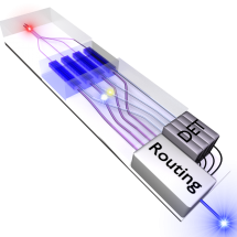 Cartoon of the four-way multiplexed light source showing on-chip photon generation and routing
Since no single optical device can perform all the required operations, the international team tackled the problem using an approach of hybrid integration – combining different optical materials and components into one device in order to exploit the best of each technology.
They combined passive glass routers created by femto second laser writing, nonlinear wave guides in a highly advanced chip, and fast optical switching elements. The photons were generated in a lithium nio bate chip
Femtos econd laser-written glass circuits produced at Macquarie were used to embed the Nice chip into the larger experiment.
“Our chip allows the generation of up to four photons simultaneously, but as they appear randomly, we can’t predict where or when the next photon will appear, lithium niobate is a wonderful nonlinear optical material, but it doesn’t interface easily with other components. The strategy of this collaboration was to use Macquarie’s laser-written waveguides both to deliver pump light to our chip and to guide the outgoing single photons towards the switching array that selects the correct output channel.” how to combine photons from two sources on a silicon chip, using ultrafast optical switches to break the intrinsic noise limit of photon sources. This new result shows that this approach is scalable – what works for a couple of sources can, excitingly, be extended to work with many – and can be applied to other types of waveguide, with more versatility in connecting different platforms.
“The laser-writing technology underlying this advance has numerous applications including quantum processing, as in this work, lasers for biology, and even the search for extra-solar planets” systems can build optical waveguides of almost arbitrary 3D form in simple glass chips. We continually find that because of this flexibility and ease of fabrication, femtosecond-written waveguides are perfect for connecting different optical systems to create a single functional device.” In the search for a single photon source, researchers in Australia and France have achieved a major step towards a turn-key source of individual, precisely tailored photons from an integrated optical chip.
A high quality source of single photons is vital for advances in quantum technologies including simulation of complex molecules, truly secure communication and ultimately quantum computation.
nature is reluctant to create photons one at a time—they tend to come out in bunches. This is a serious impediment we have to overcome in order to make photon sources a useful tool.”

Silicon Photonic Integrated Circuits (PIC) for Reconfigurable Optical Add/Drop Multiplexer (ROADM) in Multicore Fibre (MCF) Communication
New technologies to bring MCF networks one step closer to reality.
The information revolution has modified our life style in terms of work, services, medical treatment, entertainment, etc. Nowadays, optical fibre networks are capable of transmitting a large amount of information by means of short pulses of light. It has been thought that the transmission capacity of optical fibres would be inexhaustible. However, the fast increasing demands from HDTV, IPTV, rich media services, as well as business services are pushing the amount of information transmitted over traditional optical fibre networks close to their ultimate capacity limitation. Multicore fibre communication, where multiple cores are introduced in a single fibre, exploits space as a new dimension, allowing a many-fold increase of capacity. However, achieving a higher transmission capacity is only one requirement for future networks. In order to achieve a real commercial success, this new technology must also support photonic routing in future multicore fibre network nodes, where much functionality still remains to be demonstrated. This project will explore integrated solutions for the required functionalities in multicore fibre communication, targeting low loss and low energy consumption of network nodes. The project will develop a compact silicon chip integrating all the networking functionalities, aiming to demonstrate a powerful module and pushing multicore fibre communications one step closer to reality.
On-chip synthesis of circularly polarized emission of light with integrated photonic circuits
The helicity of circularly polarized (CP) light plays an important role in the light–matter interaction in magnetic and quantum material systems. Exploiting CP light in integrated photonic circuits could lead to on-chip integration of novel optical helicity-dependent devices for applications ranging from spintronics to quantum optics. In this Letter, we demonstrate a silicon photonic circuit coupled with a 2D grating emitter operating at a telecom wavelength to synthesize vertically emitting, CP light from a quasi-TE waveguide mode. Handedness of the emitted circular polarized light can be thermally controlled with an integrated microheater. The compact device footprint enables a small beam diameter, which is desirable for large-scale integration.
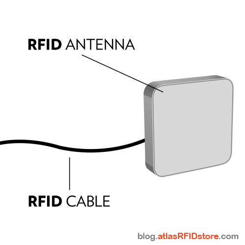
XXX . XXX 4 zero null 0 1 2 3 4 5 RFID Basics: How RFID Tags Work
RFID, or Radio Frequency IDentification, is a technology where information stored on a microchip can be read remotely, without physical contact using energy in the RF spectrum. An RFID system consists of a reader, or interrogator, which emits an RF signal via an antenna. The microchip receives the energy via an attached antenna (termed an RFID tag) and varies the electromagnetic response its antenna in such a way that information can be transferred to the reader.
Frequencies
There are several different frequency ranges used in RFID including Low Frequency (LF, 125 kHz), High Frequency (HF, 13.56 MHz), Ultra High Frequency (UHF, 433 MHz, 860-960 MHz) and Microwave (2.45 GHz, 5.8 GHz). These bands, in general, do not require a license if the transmitted power is limited. Some bands can be used globally (HF) while others are specific to certain regions (UHF in US, EU, and Japan).
Capacitive vs. Inductive
There are two modes of communication used in RFID (termed coupling), inductive coupling and capacitive coupling. Inductive coupling involves the reader emitting a magnetic field. When a tag enters the field, the chip will vary its antennas response which will result in a perturbation of the magnetic field which can be detected by the reader. The strength of a magnetic field drops sharply with distance from the emitter, hence inductive systems are inherently short range. This is the mode of operation at HF. Capacitive coupling involves the reader emitting a propagating electromagnetic wave. When this wave impinges on a tag, the chip will modify the antenna radar cross section in such a way that the reflected signal containing the information on the chip can be detected by the reader. This is the primary mode of operation at UHF and in the microwave region.
Active vs. Passive
RFID tags are termed active or passive based on how they are powered. Active tags are battery powered and will actually actively transmit a signal. Active tags have the longest read range (~100 meters) and are the most expensive due to the battery and transmitter cost. Passive tags have no on-tag power supply. The energy to activate the chip is derived solely from incoming wave from the RFID reader. The read range is limited by the transmitted power density necessary to achieve sufficient voltage for the chip to activate. Passive tags are significantly less expensive than active tags and, in general, will have significantly less range. A third class of tags are semi-active, or battery assisted passive (BAP) tags. These tags include a battery so the chip will always have sufficient energy to turn on but they do not have an active transmitter. Since, in general, the limiting factor on the read range of a passive tag is getting sufficient power to the chip, BAP tags have greater range than passive tags although at a higher cost and limited life due to the battery.
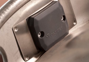
Read on Metal
 At UHF frequencies, most RFID tags are a variation on a standard dipole antenna design. The antenna is designed to provide a good “match” to the microchip. This enables a smooth flow of energy captured by the antenna to the chip enabling it to turn on. Unfortunately, dipole antenna performance is greatly affected by the electromagnetic properties of materials in the vicinity. This problem becomes acute when metal is nearby. The presence of metal will change the antenna’s properties such that there is no longer a good “match” and power will not flow to the chip and the tag can not be read. To overcome this obstacle companies, such as companies that produce Custom Tags, have developed special “backings” to separate RFID tags from metal surfaces. RFID tag technology has evolved to the point where the read range of on metal RFID tags rivals that of their non-metal-mount counterparts.
 Operating Principles: Coupling
Understanding the way that an RFID system communicates, at least on a basic level, is a necessity—especially for deployment. RFID knowledge, together with extensive testing, is the key to a successful RFID implementation. Tag and reader communications rely on two scientific principles: physics and electromagnetism. In RFID systems, readers and tags communicate mostly through the method of electromagnetic coupling.
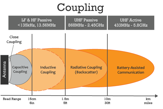
In order for an RFID tag to communicate with an RFID reader/antenna, the tag circuit and reader circuit generally must couple in some way. Coupling is a transfer of energy between two electronic items or two circuits. Two main types of coupling are present in RFID systems: capacitive and inductive. The way that the two circuits couple can determine the read range and frequency of the system. Defined below are coupling techniques along with some frequently used terms in the industry relating to communication.
Capacitive Coupling – flush to 1-2 cm – systems that use capacitive coupling use electric currents instead of the magnetic field in order to couple. Contact to a few centimeters of read range is normal for (LF) or Low Frequency communication because of the need to produce an electric field using electrodes. Because this type of coupling is only effective at such a small proximity, it is not used by very many RFID systems on the market today. One application example is access control/smart cards.
Close Coupling – Close coupling can employ electric or magnetic coupling depending on the reader and tag. Readers employed for close coupling using a magnetic field have a winding primary coil and when the tag is in close proximity (0.1 cm – 1 cm) the secondary winding coil of the tag combines with the primary coil via their shared magnetic field in order to communicate. Readers and tags that use electric-field coupling are constructed so that the coupling surfaces when brought together, and inserted parallel, form an electric current for communication.
Inductive Coupling – 1 cm to 1 m – Inductive coupling relies on the magnetic field of the reader, which means that this coupling only occurs in the near-field. The size of the near-field is dependent on the reader, but can be generally defined as touch up to a meter. Inductive coupling is seen in LF, HF, and UHF applications that include coils/antennas in the tag infrastructure. Increasing the amount of loops of wire (coils) in a tag that uses inductive coupling increases the amount of current that would be generated in the tag. In turn, this would increase the power of the transmitted signal from the tag back to the reader. Some example applications include NFC Smart Posters, certain access control applications, and any UHF application with a read range under 1 meter in length.
Magnetic Coupling – the term magnetic coupling refers to any coupling that occurs using the reader and tag’s magnetic field (see inductive coupling).
Radiative coupling (backscatter) – 1 m to +4m – Using backscatter to communicate between readers and tags is not a true method of coupling; it is actually a communication method involving electromagnetic waves. Electromagnetic waves are sent through the air from the reader antenna to the tag antenna. The energy is received by the tag antenna and a small amount energy is then reflected back to the reader. Most UHF systems use backscatter in order to communicate between tag and reader. One common exception is when the tag and reader are in close proximity. When in close proximity, UHF RFID systems will elect to couple magnetically/inductively. Race timing, asset tracking, and file tracking are three applications that use backscatter for reader tag communication.
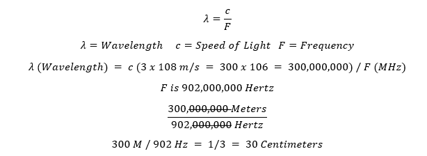
Understanding Near-Field and Far-Field Antennas
The electromagnetic field that surrounds an RFID antenna can be broken up into two segments – near-field and far-field. Typically, near-field is defined as the field around the antenna up to one wavelength (λ) away (approximately up to 35 centimeters). The two segments of the RF field, near-field and far-field, have different energies so they typically require a corresponding antenna type to get the best read range. (The near-field is primarily magnetic in nature, while the far-field has both electric and magnetic components.)
The communications between an RFID tag and an RFID reader (via the antenna) occurs using a process known as electromagnetic coupling. There are two types of coupling – inductive and capacitive.
INDUCTIVE:
A near-field antenna uses inductive coupling which means that it uses a magnetic field to energize the RFID tag. A magnetic field is created in the near-field region that allows the RFID reader’s antenna to energize the tag. The tag then responds by creating a disturbance in the magnetic field that the reader picks up and decodes.
CAPACITIVE:
A far-field antenna uses capacitive coupling (or propagation coupling) to energize the RFID tag. Capacitive coupling occurs when the RFID reader’s antenna propagates RF energy outward and that energy is used to energize the tag. The tag then sends back a portion of that RF energy to the reader’s antenna as a response which is known as backscatter.
With a low profile and a small form factor, a near-field antenna is perfect for short read range applications. Unlike far-field antennas which send out a propagating electromagnetic field, near-field antennas generate a local magnetic field. Additionally, near-field antennas are typically less rugged than far-field antennas and usually intended for indoor environments. As near-field antennas are less commonly used, there are limited options available for deployment.
Far-field antennas come in a wide variety of shapes and sizes and generally can read tags between a few centimeters, up to more than 30 feet away in ideal conditions. Plenty of options are available when selecting a far-field antenna such as linear or circular polarization, varying gain, and options for indoor or outdoor use. Due to the increased read zone when using far-field antennas, stray tag reads (i.e. reading unintended RFID tags) tend to be a common issue.
RFID Tag Antennas
RFID tag antennas are designed for a unique purpose, and their design can actually reveal some information about the tag itself. Below are a few things you can usually learn from looking at an RFID tag:
- Its frequency: You can discover whether the tag is Low Frequency, High Frequency, or Ultra-High Frequency, and then have a general idea of the tag’s read range.
- If the tag is a Far-Field tag and if it has additional Near-Field capabilities.
- If it is a UHF Dipole – the type of dipole antenna used: Fat, Meandered, or Tip-Loaded.
Frequency
Generally, if you know what to look for it is pretty easy to detect the frequency at which the tag operates just by examining the tag. That is because the correlation between the tag antenna design and the way the tag talks to the RFID reader/antenna will reveal the frequency. Below, the three main frequency types are outlined, including information about each and their typical antenna design:
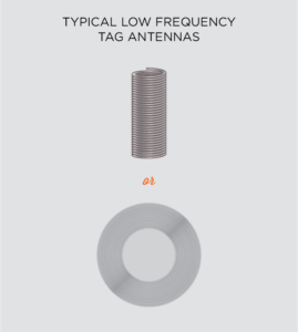
Low Frequency (LF)
- Frequency: 125 – 135 kHz – generally, 124 kHz, 125 kHz, or 135 kHz
- Read Range: Touch to 45.7 cm (18 in) under ideal conditions
- Coupling Technique: Inductive coupling – reader’s antenna generates a magnetic field to activate an electric current in the tag’s antenna
- Antenna Design: Typically, circularly coiled tag antenna
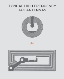
High Frequency (HF)
- Frequency: 13.553 – 13.567 MHz – generally, 13.56 MHz
- Read Range: Touch to around 1.5 m (5 ft.) under ideal conditions
- Coupling Technique: Inductive coupling – reader’s antenna generates a magnetic field to activate an electric current in the tag’s antenna
- Antenna Design: typically, rectangular or circular-shaped, small tag antenna
Ultra- High Frequency (UHF)
- Frequency: 400 – 1000 MHz – generally, 860 – 960 MHz
- Read Range: Up to 35 m (115 ft.) under ideal conditions
- Coupling Technique: Backscatter coupling – reader’s antenna generates RF energy to activate the RFID tag, which modulates the information and reflects the remaining energy back to the reader antenna.
- Antenna Design: Typically, dipole-shaped tag antenna
- Near-Field Capabilities: If it has a small loop-shaped antenna in the middle, it usually has near-field capabilities.
UHF Structure & Materials
Most UHF tag antennas are designed with a dipole-type structure. This means they generally are long and thin visually, and operate similar to a magnet. The similarity is apparent because they have two ‘open’ ends, or poles, for the energy to build up and, consequently, allow a current flow to the Integrated Circuit (IC), or chip.
The most well-known RFID tags on the market that are not structured like a typical dipole antenna are tags similar to the SMARTRAC Frog and the Alien Spider. These tags are square-shaped in order to best display their omni-directional properties and are sometimes called “dual-dipole” tags.
Tag antennas are made from a metal wire or metallic sheet in order to provide an adequate conductor for the RF energy. Then, depending on the type of tag, other types of materials like PET, plastic, paper, and polyester are used to provide the base around the tag antenna.
Terms to Know
AC – an electrical current that sometimes changes its direction, usually 50 to 60 times per second.
DC – an electrical current that flows constantly in one direction.
Resistance – the property of a particular material to resist the flow of electrons. Occurs in AC and DC circuits.
Inductance – the property of an electric conductor that causes an electromotive force to be generated by a change in the current flow.
Capacitance – the ability of a body to store electric charge.
Resonance – a state achieved when the inductance and capacitance cancel each other out.
Reactance – the property of a particular material to resist the change in flow of electrons, only in AC circuits. Below are two different types of reactance:
Inductive Reactance – the ability to store energy in the form of a magnetic field. Below is the equation:
ω (Angular Frequency) = 2πF
XL = 2πFL = ωL
Capacitive Reactance – the ability to store energy in the form of an electric field. Below is the equation:
ω (Angular Frequency) = 2πF
XC = 1 ÷ (2πFC) = 1 ÷ (ωC)
Impedance – the combination of resistance and reactance.
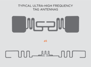
UHF Dipole Lengths
The length of a UHF dipole antenna is one way to effectively classify that type of dipole. Three common dipole lengths exist: Half-Dipole, Modified Half-Dipole, and Short-Dipole. In order to distinguish the difference, first the wavelength typically associated for UHF RFID tags must be found:
Half-Dipole – A Half-Dipole’s length is equal to one-half of the wavelength. With a UHF tag, a typical size for a half-dipole is around 16.4 centimeters (164 mm) or anywhere between 16 and 17 cm. These are typically not used in RFID applications because the tags would be too long and tend to have resistance problems.
Modified Half–Dipole – A Modified Half-Dipole’s length is usually around 9.2 cm (92 mm). This length is convenient because most printer labels are around 10.6 cm (106.2 mm) so the tag can easily fit on or in them. Because a length shorter than a half-wave dipole has a negative reactance, several things have to be modified to make this shorter antenna work. These tag antennas can also be referred to as “Dipoles” or “Resonant Antennas”.
Short Dipole – A Dipole that is typically 1/10 of the wavelength in size is referred to as a Short Dipole. These are much smaller than Half-Dipoles and have to be modified greatly in order to work well because of their size.
Dipole Types
Because Modified Half-Dipoles are smaller than half of a typical UHF wavelength, they have a negative inductance and must be modified with additional capacitance to counter balance; or, inductance can be added, lowering their resonance to a lower frequency. Modifying these antennas is usually performed one or two of the following ways:

Fat – “Fat” dipoles, also called “Broadband” dipoles, are characterized by having the maximum amount of metal on the tag face. Increasing the amount of metal on the tag is achieved by etching or silver ink printing. By increasing the wire thickness, inductance is reduced, and the increased metal surface creates a large capacitance. Because these tags have a lot of metal, they are often best used on high dielectric surfaces like glass, wood, and plastic.
One of the most popular fat or broadband UHF tags on the market is Alien’s “G”. The Avery Dennison AD-661r6 is also a fat tag.

Meanders – Most people associate meanders with UHF RFID tags even if they do not know why the meanders are on the tag. Meanders are the typical product of folding the wire back and forth, creating peaks and troughs along the wire. These meanders are lengthening the actual wire without adding length to the tag. This means a wire length of a half-wavelength dipole (16.4+ cm) is possible while still being able to fit on a typical printed label (10.2 cm). The meanders lower the resonance and allow the tag to resonate at the preferred frequency.
Some of the most common examples of tags with meanders are the Alien Squiggle, the SMARTRAC ShortDipole, and the Avery Dennison AD-321r6.

Tip Loading – Tip Loading looks similar to a fat dipole and is usually used in conjunction with meanders in order to drop the resonance. Tip loading is adding metal through etching or silver printing to the ends of the dipole only. Adding wide metal ends to a dipole allows additional storing capacity for electric charges, which compensates for the reduced inductance because of the length.
The Best RFID Tag For Your Application
Passive RFID tags electronically store data enabling RFID readers and antennas to identify and track objects. Each RFID tag has specific attributes that define its limitations physically, environmentally, and mechanically. When applied to a particular RFID system’s requirements, these limitations help narrow down the search to find the optimal tag. The seven attributes below should be considered when selecting an passive RFID tag.
 Frequency Range

Similar to the other parts of an RFID system, RFID tags should be tuned to the correct frequency range for the country in which they are deployed. If the reader is transmitting on the 902-928 MHz band and attempts to read tags tuned to the 865-868 MHz band, the tags will not respond.
Key Takeaway: Consider the operating region regulations for your application and select a tag compatible with the specific region.
Environment
If your application must endure extreme temperatures, sand, water, dirt, or an intensive laundering process, it is essential to select an RFID tag that is built to withstand such conditions.
Key Takeaway: Consider all environmental factors and check them against the tag’s specifications. There are many specialty RFID tags developed to survive extreme conditions of all sorts.
Mounting Surface

Each RFID tag is designed to be applied to a specific set or sub-set of materials. RFID tags generally work well on materials such as plastic, wood, or cardboard, but only certain tags have the ability to work well on more complex materials such as metal or glass. Tags that can be mounted on metal or glass usually cost more than typical RFID labels or inlays.
Key Takeaway: Consider the mounting surface to which the tag will be applied.
Size
RFID tags are manufactured in different sizes and shapes to better accommodate for unique applications. Depending on the specific application and the amount of space on the object to be tagged, size can play a critical role in determining the ideal tag. Some applications are hampered by the lack of available room on an object, such as tagging medical and surgical instruments.
Key Takeaway: It is important to understand how much surface area is available when selecting an RFID tag.
Attachment Method
The material and shape of the item to be tagged are two of the most important aspects to consider when determining the appropriate attachment method. Some tags will work well with all-purpose adhesives and epoxy, while other tags will need to be adhered with rivets, screws, or welding equipment. Objects such as cardboard boxes typically will be tagged using general purpose adhesive, while metal pallets might require rivets or screws.
Key Takeaway: Attachment methods for a given tag are typically found within the tag’s datasheet.
Read Range
An RFID tag’s read range is a crucial component of almost all RFID systems. However, there are many factors that affect read range – such as antenna gain, reader transmit power, and tag orientation – and each should be considered when determining the optimal range for your application.
Key Takeaway: Consider the read range your application requires and test a variety of tags to ensure success.
Custom Printing & Encoding
Custom printing and encoding do not necessarily narrow down the RFID tag choices; however, both are important to consider before purchasing. If your application is customer facing, custom printing may be a feasible option to keep your tags looking professional with a logo or a barcode on the front. Custom encoding may be beneficial if you lack the time, equipment, or manpower to encode your RFID tags with a custom sequence of data. Access control applications are a primary example of where custom encoding plays a crucial role.
Key Takeaway: Consider if your application may benefit from custom labeling or encoding of RFID tags.
The Importance of Selecting the Right Attachment Method for RFID Tags
Just about any type of inventory or asset – regardless of shape, material type, or use – can be tracked using RFID tags. The key to tracking different types of items is choosing the right RFID equipment, especially the right RFID tags.
Equally as important as selecting the correct RFID tag, selecting the right attachment method can make the difference between a successful application and a failed application. If the wrong attachment method is chosen, the tag could fall off and skew the application’s efficiency.
Several methods are available for securing an RFID tag to an asset as shown in the chart below.
| General Purpose Adhesive | Extra Strength Adhesive | Epoxy |
| Embedding | Shrink Wrap | Cable Ties |
| Screws or Bolts | Rivets | Welding |
| Sewing | Hanging | Straps |
Consider the following aspects in order to narrow down the attachment method options.
Tag Attachment Options – Some tags will only have a few feasible attachment methods, while others might can use almost any attachment method available. If a given tag meets all other application requirements (i.e. read range, memory, size, etc.), check the recommended attachment methods for that specific tag on the tag’s data sheet or by asking the manufacturer.
Surface Material – The asset’s surface material is a key component in choosing an attachment method because some attachment methods will work better on certain types of materials. For example, adhesives and welding are two examples of attachment methods better suited for metal assets than textiles or linens. The asset’s surface material, whether that be metal, wood, plastic, or cotton, should be taken into consideration in order to narrow down the available attachment options.
Of note, when using adhesive and before attaching a tag to an item, always clean the intended tagging area so that the tag has the best chance of staying securely attached for the application’s lifespan.
Exposure – If the tag will be exposed to any harsh environmental concerns such as UV light, moisture, vibration, pressure, chemicals, or impact, its attachment method will be exposed as well. If one of these concerns applies to your application, it is best to choose an attachment method that has been tested and proven to withstand such exposure.
Temperature – Extreme temperatures are important to consider when choosing a tag and attachment method. Not only could the tag be damaged and become unreadable, but the actual method of attachment could melt off the item (e.g. adhesive) or become brittle and break (e.g. cable tie) causing the tag to fall off the item. Be sure that the attachment method has been tested in application temperature conditions before making a final selection.
In addition to the environment, temperature of the item itself should also be assessed when choosing the attachment method. If the environment is a normal, regulated temperature, but the actual item can reach much higher or lower temperatures, take the more extreme temperature into consideration when choosing how to attach the RFID tag.
Application Lifespan –Certain attachment methods can slowly degrade over time depending on their chemical makeup. In applications that have assets with a long lifespan, such as returnable transit assets (e.g. reusable pallets), the tag may need to stay on the asset for years. Evaluate the tag and attachment method to make sure that they are compatible with the intended lifespan of the asset in the application.
5 Ways to Attach RFID Tags
If you don’t properly attach your RFID tags to different surface types, your read rate will suffer, therefore limiting the effectiveness and efficiency of your RFID implementation. Without the ability to consistently read your RFID tags, you will not be able to uniquely track and identify assets.
By choosing the right RFID tag for your application, you will greatly improve read rates. Depending on the asset’s surface and environment, you will need to select an RFID tag with an appropriate method of attachment.
These five methods are commonly used to affix RFID tags to assets:
- Film Adhesive: Used for most tags and standard applications such as race timing and tracking fixed IT assets.

SMARTRAC DogBone RFID Tag
- Film Adhesive: Used for most tags and standard applications such as race timing and tracking fixed IT assets.
- Foam Adhesive: Typically used with more rugged tags and in applications where a stronger adhesive method is required, such as tracking fixed durable assets.
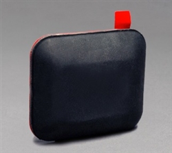
Omni-ID Curv RFID Tag
- Foam Adhesive: Typically used with more rugged tags and in applications where a stronger adhesive method is required, such as tracking fixed durable assets.
- Epoxy: Used to cover embedded tags or any tags where you need the strongest possible adhesive, like tool tracking.
Xerafy Pico-iN RFID Tag
- Epoxy: Used to cover embedded tags or any tags where you need the strongest possible adhesive, like tool tracking.
- Screws/Rivets: Used in conjunction with durable tags in applications where you need the strongest possible attachment method, such as mobile durable assets.
Confidex Ironside RFID Tag
- Screws/Rivets: Used in conjunction with durable tags in applications where you need the strongest possible attachment method, such as mobile durable assets.
- Wire or Cable Tie: Used where any of the above options are not feasible. Not a very durable form of attachment, but it is good for hard to tag items, like cables or cords.
RFID Hang Tag
Which Applications Need High Memory RFID Tags?
The best way to answer this question may not be necessarily to call out specific applications that may (or may not) need high memory – for example, asset tracking, etc. Rather, a better way to determine if an application needs high memory RFID tags, is to determine if the application will be able to have reliable access to a database (as needed) in order to pull up relevant information about the tagged object.
Because a database can theoretically store as much information as required about any given tagged object, as long as the user has access to that database, the only thing a tag really needs is a unique ID within that application. In such a case, the user would simply read the RFID tag and then be able to pull up as much information as needed (assuming the user interface is designed accordingly). The database access could occur in real-time if the RFID reader is connected to a network, but can also occur if, for example, a user has a mobile RFID handheld reader that has a local copy of the database. (In this example, the local database would need to periodically sync with the master database.)
In the event that reliable database access isn’t possible and the user must store data about the tagged item, then storing data on the tag itself may be the best option and this is when high memory RFID tags would be needed.
Types of Memory in RFID Tags
Q: In UHF Gen 2 tags, what are the different types of memory and how will I know when to use each type?
A: Gen 2 RFID tags are comprised of an antenna and a chip (more accurately called an integrated circuit, or IC). The ICs for Gen 2 tags contain four types of memory:
- Reserved memory
- EPC memory
- TID memory
- User memory
When starting your application and selecting a tag, in order to know about how much memory is on each tag’s IC, you can check the specifications page on each tag’s data sheet. To learn the properties of each memory bank, we have outlined them below:
Reserved Memory:
This memory bank stores the kill password and the access password (each are 32 bits). The kill password permanently disables the tag (very rarely used), and the access password is set to lock and unlock the tag’s write capabilities. This memory bank is only writable if you want to specify a certain password. Most users do not use this memory area unless their applications contain sensitive data. It cannot store information besides the two codes.
EPC Memory:
This memory bank stores the EPC code, or the Electronic Product Code. It has a minimum of 96 bits of writable memory. The EPC memory is what is typically used in most applications if they only need 96 bits of memory. There are some tags that have the capability of allocating more bits to the EPC memory from the user memory. EPC memory is your first writable memory bank.
TID Memory:
This memory is used only to store the unique tag ID number by the manufacturer when the IC is manufactured. Typically, this memory portion cannot be changed.
User Memory:
If the user needs more memory than the EPC section has available, certain ICs have extended user memory which can store more information. When it comes to user memory, there is no standard in how many bits of memory are writable on each tag. Typically, the extended memory is no more than 512 bits, but there are some high memory tags with up to 4K or 8K bytes of memory. This is the second writable memory bank for Gen 2 ICs.
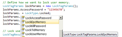
Locking Memory on EPC Gen 2 RFID Tags
Locking the memory on EPC GEN 2 compliant RFID Tags is an often misunderstood process. Many think that it is simply a matter of changing the access password to a non-zero value (the default for Gen 2 tags) and then the tag is ‘locked’ but this is not the case. This posting will review how tag locking works for EPC RFID tags and show you how to lock the Impinj Monza tags using .NET version 1.0.0.6 of the Octane Software Development Kit (SDK).
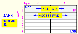
GEN 2 TAG PASSWORDS
An EPC GEN 2 tag has two separate passwords — an access password and a kill password; each are 32 bits, and are stored in the reserved bank (bank 00) of the tag memory.
STATES
When a tag is singulated, it enters one of two states:
1. Secured (if access password is all zeros, which is the factory default)
2. Open (if non-zero access password has been programmed to the tag)
2. Open (if non-zero access password has been programmed to the tag)
A tag in the open state can be moved to secured by providing the previously programmed non-zero access password.
The key thing to remember is that assigning a non-zero access password does not, in itself, prevent anyone with a GEN 2 RFID reader from reading or changing data on the tag. It only requires that any future users must provide the access password in order to change the lock state and is simply one step in effectively locking tag memory.
Each memory bank can be in one of four lock states:
1. Unlocked
2. Perma-unlocked (can never be locked)
3. Locked
4. Perma-locked (can never be unlocked)
2. Perma-unlocked (can never be locked)
3. Locked
4. Perma-locked (can never be unlocked)
This is illustrated below when programming the lock state of the tag.

LOCK PROCEDURE
The steps for locking a Gen 2 RFID Tag are (for a factory default tag):
1. Lock (or perma-lock) the selected memory bank using default password of all zeros.
2. Assign a 32 bit (8 hex character) access password. (This will prevent the tag lock state from being changed.)
3. Lock the access password. (This will prevent the password from being read or over-written.) Not doing this step would allow any user to simply read the access password, then use it to unlock and over-write memory on the tag (unless it has been perma-locked).
Only the reserved memory bank (access and kill passwords) can be both WRITE and READ locked – all others (EPC, TID, and User) can be write-locked only. Typically the Tag Identification (TID) memory bank is perma-locked at the factory.
Each tag memory bank can be individually write locked as shown below.
SAMPLE CODE
Here is an example of locking user memory in C# using the Octane SDK.

OTHER USEFUL NOTES
In addition to the increased memory size, the Impinj Monza 4QT tag chips offer the ability to independently lock four fixed, 128-bit sections of user memory (block permalock). This feature is particularly useful for situations such as in a supply chain, where various participants along the chain may want to record data, but not necessarily have it be openly available to all parties.
Lock status cannot be read, it can only be inferred. So there is no direct way to query a tag and have it reply if it is locked or not. However, in some cases when attempting to access a tag memory bank, it will return a pretty specific error “tag memory locked”.
RF Physics: How Does Energy Flow in an RFID System?
RF Physics & RFID: A Brief Overview
RFID systems, like all systems involving energy, are governed by the laws of physics. Physics is the study of matter and its motion through space and time, along with related concepts such as energy and force. To delve deeper, RFID systems also are subjected to fundamental electromagnetic principles. These principles speak to the transfer of energy and the electromagnetic spectrum, are defined in Faraday’s Law of Electromagnetic induction and Lenz’s Law. In addition, governments and military departments regulate the use of the electromagnetic spectrum (frequency and power of transmission) in various parts of the world, which leads to different standards and regulations governing RFID systems.
Every aspect of an RFID system is designed using the laws and standards as stated above in order to successfully exchange information using an electromagnetic field and modulated energy. Each part of the process – reader to cable, cable to antenna, and antenna to tag (and back) ensures effective energy transfer between the segments.
Each step in the energy flow process of a typical UHF RFID system is simply defined below.
Energy Flow: Reader to Cable
Energy flows out of an electrical outlet as AC power (Alternating Current power) which means electrons periodically reverse directions as they are traveling, enabling the energy to be transmitted longer distances relative to DC power (Direct Current power). A typical RFID reader power supply included with an RFID reader is an AC to DC power converter, changing the alternating current from the outlet to a direct current (which is more suitable for the reader electronics).
Next, the direct current runs through an Oscillator and Phase Locked Loop (PLL) module which then converts the direct current from the power supply to an alternating current at a variable frequency. The variable frequency is determined by a frequency hopping algorithm inside the RFID reader, which is based upon the frequency range set during the manufacturing stage.
For example, in the United States, each reader is required to employ a frequency hopping algorithm due to regulations stating that a single reader cannot transmit on a specific frequency for more than 400 milliseconds or 0.4 seconds in order to prevent crowding specific frequencies. While using an RF reader set for the US FCC frequency range, the reader will ‘hop’ every 0.4 seconds in a predetermined pattern such as 902.5 MHz (0.4 s), 903.5 MHz (0.4 s), 927 MHz (0.4 s), and so on. If a reader were to stay on one frequency for longer than 0.4 seconds there could be interference between neighboring radios.
After the value of the variable frequency has been set, the resulting signal is then amplified using the RF amplifier and modulated by the information that the reader is attempting to send to the RFID tag. An RF amplifier determines the power of the signal to be transmitted by the RFID reader (i.e. its transmit power) and amplifies the RF signal to that desired power level. According to US FCC regulations, the power signal sent from the reader cannot exceed 1 watt (30 dBm). However, because the power from the antenna includes attenuation due to cable loss, some RFID readers are able to transmit power levels of over 30 dBm (for example, 31.5 dBm). The attenuation of the cable then negates the extra transmit power enabling the reader not to be in violation of FCC standard 15.247. When using reader transmit power levels of > 30 dBm, operators need to ensure that the cable being used will provide the required attenuation so that the power input into the antenna does not exceed 1 Watt. (Check out the GS1 document, for more specifics on regulations for UHF RFID in other countries.)
The amplified signal is then passed through an RF Bandpass Filter that eliminates any additional frequencies that are outside of the allowed transmission band. After passing through the Bandpass Filter, the signal is then output to the antenna port and, subsequently, to the coaxial cable through a directional coupler.
Energy Flow: Cable to Antenna
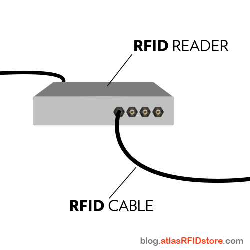
The signal is then conducted through a coaxial cable into the RFID Antenna. Of note, power is lost in this process due to the attenuation of the signal as it travels along the cable. The amount of power lost depends on the length of the cable and its insulation rating. Lower loss cables are usually thicker and shorter in length. [Read more about Getting the Most from Your RFID Cable.]
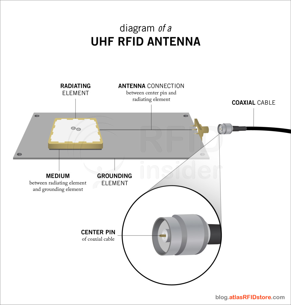
When the coaxial cable is properly connected to the antenna port, the center pin of the cable connector is connected to the radiating element of the antenna. The signal (or AC current) flows from the center pin, to the radiating element, and then through the medium to the grounding element (see diagram below). The radiating element in conjunction with the ground plane focuses the energy based on the gain parameters of the antenna in order to build the electromagnetic field.
When the electromagnetic field is built, the radiating element releases the electromagnetic waves, which propagate out from the antenna. The shape and form of the radiated energy is called the radiation pattern of the antenna.
The beamwidth of the antenna can be calculated from the radiation pattern of the antenna. Beamwidth is the angle between the half power points of the main lobe of the radiation pattern. The radiation pattern, beamwidth, and gain are all affected by the size of the grounding plate as well as the size of the radiating plate.
Energy Flow: Antenna to Tag (and Back)
The propagated waves travel in space to a distance vertically and horizontally based on the specific gain and beamwidth parameters of the antenna.
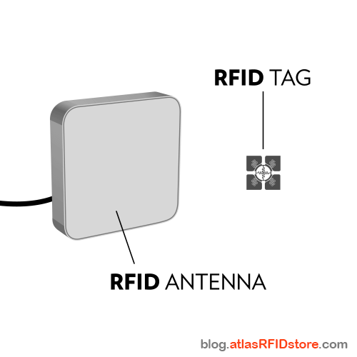
The RFID tags in the field receive the energy, or RF waves, using their own antennas. The energy received travels through the RFID tag’s antenna and a portion of it is used to activate the chip (i.e. the Integrated Circuit, or IC) and prepare for transmission of data based on commands received from the RFID reader.
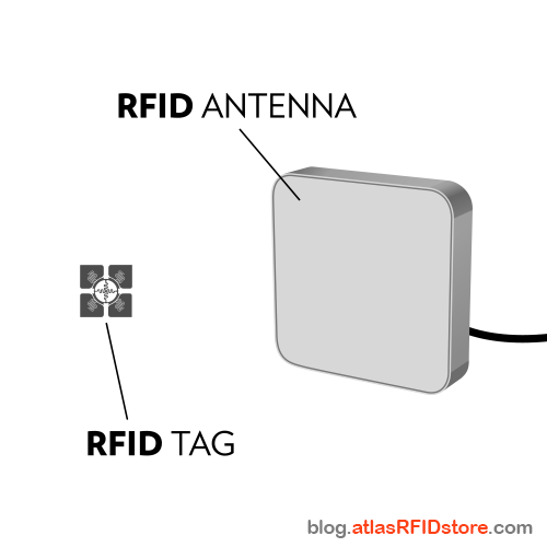
When the chip is turned on, it modulates the energy with the information stored in the tag (pertinent to the reader’s request) and “reflects” the remaining energy back. This information could be EPC memory, User Memory, or anything programmed on the tag. This reflection of energy back to the antenna is known as backscatter radiation.
The backscatter radiation travels through the air, into the RFID antenna’s field, and back through the coaxial cable into the antenna port on the RFID reader. The directional coupler picks up the received signal and passes it through the bandpass filter, a mixer, and a baseband amplifier to a decoding circuit to recover the tag’s information.
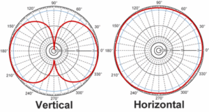
RFID Antennas: Beamwidth & Directivity
Even though RFID antennas are not the brains of an RFID system, they are still complex devices that can hinder or benefit an RFID system depending on the application and chosen antenna. For instance, choosing the wrong antenna for a certain application could result in inches of read range instead of feet. Besides the basic guidelines for choosing an antenna like gain and polarization, other factors exist that could take a system’s read range and results to the next level. Beamwidth and directionality are two core principles to grasp in order to make a more informed purchasing decision.
Beamwidth
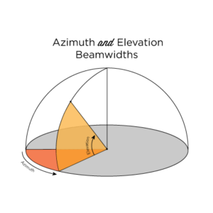
Beamwidth is defined as “the angle between two points on the same plane where the radiation falls to ‘half power’, or 3 dB below the point of maximum radiation.”¹. It can also be thought of as the peak effective radiated power of the main lobe. Most usually think of beamwidth as the horizontal angle on a radiation pattern, but there are two beamwidths – azimuth (horizontal) and elevation (vertical).
Azimuth vs. Elevation
If the antenna is on a 3D plane, like below, you will be able to accurately see the azimuth and elevation beamwidths. Understanding the azimuth and elevation beamwidths of an RFID antenna enables a person to choose the best antenna for their application. In some applications, a very wide azimuth or elevation beamwidth is needed in order to read all the tagged items lined up in, for example, a small room. In other applications, like a conveyor belt, a thinner, acute beam is better fitted. Some antenna data sheets actually show the 3D model of the azimuth and elevation beamwidths, while other manufacturers’ data sheets show 2D models. The 2D models are more basic, but are still able to clearly show the beamwidth in both planes.
Directivity
The directivity of antenna is defined as “its ability to focus in a particular direction to transmit or receive energy”¹. The way that an antenna directs its energy is a huge factor in both choosing an antenna and setting up an application. If an antenna is set up in an application and the type and radiation pattern is not known, the tagged items might not be read or be affected by absorption, diffraction, reflection, and refraction. Antennas can be grouped in two different sets based on directivity – isotropic or anisotropic, or omni-directional or directional.
Isotropic vs. Anisotropic
Another important concept to understand about antennas is there are two main types in terms of beams and directionality: isotropic and anisotropic. An isotropic antenna is one which emits an RF field uniformly in all directions. A perfect isotropic RFID antenna, or one that emits radio waves in general, doesn’t exist because the concept violates Maxwell’s equations. Even though there are no true isotopic antennas available to purchase, it is still beneficial to understand the concept because it can aid when learning about gain.
If gain is written as dBi instead of dBd it is being displayed over the value rate of an isotropic antenna. The true gain rating of an antenna is displayed in dBd. Because isotropic antennas radiate equally in all directions, portraying the gain in dBi is essentially just inflating it. In order to compare different antenna gains displayed in dBd and dBi, use the formulas below.
dBi = Antenna Gain in dBd + 2.14 dB
An anisotropic antenna just implies the opposite of isotropic and is defined as an antenna that radiates power differently and unequally in the elevation and azimuth fields. All antennas sold are anisotropic.
Omni-Directional vs. Directional
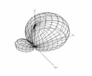
Omni-directional and directional antennas differ in the directionality of the beam. Omni-directional antennas are used mostly in proximity antennas but can be in other types as well. These antennas are built to increase the coverage of the azimuth plane and decrease coverage in the elevation plane; this is done by emitting RF power in a spherical pattern. In a 3D model, the beamwidth of these antennas look like a donut or a sphere and they usually have a mid-level gain.
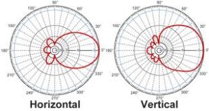
Directional antennas are more common and usually have external antennas. Directional antennas emit concentrated RF power toward a targeted area. These antennas sometimes have an azimuth and elevation beamwidth of roughly the same degree in order to provide the perfect ‘beam’ of coverage. The beamwidth (azimuth or elevation) is determined directly by the gain of the antenna– the higher the gain, the more focused the beam. All types of directional antennas exist with different azimuth and elevation angles and gains. Understanding the beamwidth, gain, directionality, and how each of these interact to create a radiation pattern will help when choosing the best antenna for an application.
Both omni-directional and directional antennas are commonly sold on the RFID market. In an application where tagged items will be passing the antenna on different sides, or even near the back, an omni-directional antenna would be the best choice. Omni-directional antennas are also used in any application where a wide angle of coverage is needed. Directional antennas are great for applications where the tagged items will always be passing the same area at around the same height, like a conveyor belt. It is easy to think of directional antennas as more targeted antennas with cone-like beams.
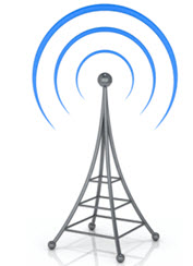
XXX . XXX 4 zero null 0 1 2 3 4 Wi Fi Working Principle, Types of Technologies and Applications
A Brief Introduction About Wi-Fi:
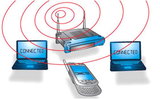
Wi-Fi is a popular wireless networking technology. Wi-Fi stands for “wireless fidelity”. The Wi-Fi was invented by NCR corporation/AT&T in Netherlands in 1991. By using this technology we can exchange the information between two or more devices. Wi-Fi has been developed for mobile computing devices, such has laptops, but it is now extensively using for mobile applications and consumer electronics like televisions, DVD players and digital cameras. There should be two possibilities in communicating with the Wi-Fi connection that may be through access point to the client connection or client to client connection. Wi-Fi is a one type of wireless technology. It is commonly called as wireless LAN (local area network). Wi-Fi allows local area networks to operate without cable and wiring. It is making popular choice for home and business networks. A computer’s wireless adaptor transfers the data into a radio signal and transfers the data into antenna for users.
Working Principle:
Wi-Fi is a high speed internet connection and network connection without use of any cables or wires. The wireless network is operating three essential elements that are radio signals, antenna and router. The radio waves are keys which make the Wi-Fi networking possible. The computers and cell phones are ready with Wi-Fi cards. Wi-Fi compatibility has been using a new creation to constituent within the ground connected with community network. The actual broadcast is connected with in sequence in fact it is completed by way of stereo system surf as well as the worth of wires with monitor to classification prone. Wi-Fi allows the person in order to get access to web any place in the actual provided area. You can now generate a system within Resorts, library, schools, colleges, campus, personal institutes, as well as espresso stores as well as on the open public spot to help to make your company much more lucrative as well as interact with their own customer whenever. Wi-Fi compatibility can make surf with stare to company using their inspiring cable television much a smaller amount force down.
The radio signals are transmitted from antennas and routers that signals are picked up by Wi-Fi receivers, such has computers and cell phones that are ready with Wi-Fi cards. Whenever the computer receives the signals with in the range of 100-150 feet for router it connect the device immediately. The range of the Wi-Fi is depends upon the environment, indoor or outdoor ranges. The Wi-Fi cards will read the signals and create an internet connection between user and network. The speed of the device using Wi-Fi connection increases as the computer gets closer to the main source and speed is decreases computer gets further away.
Many new laptops, mobile phones have inbuilt Wi-Fi card you don’t have to do any thing which is one of the best thing. If it is a free- based type of network connection the user will be promoted with a login id and password. The free base network connections also well in some areas. The Wi-Fi network connection is creating hot spots in the cities. The hot spots are a connection point of Wi-Fi network. It is a small box that is hardwired in to the internet. There are many Wi-Fi hot spots available in public places like restaurants, airports, and hotels offices, universities etc.
Security:
Security is impartment element in the Wi-Fi technology. Security is our personal decision but having a wireless connection we should pay attention to protect our private details. We can connect easily to unsecured wireless routers. The problem is any one is connected to your wire less router using the data like download games, download apps and planning terrorist activities, shirring illegal music and movie files etc. So it is necessary to provide security to the wireless technologies based devices.
How to make the Security?
All routers have a web page that you can connect for configuring the Wi-Fi security. And turn on WEP (Wire Equivalence Privacy) and enter a password and remember this password. Next time when you will connect your laptop Wi-Fi router will ask you to enter the connection password and you enter that password.
Types of WI-FI Technologies:
Currently they are four major types of WIFI technologies.
- Wi-Fi-802.11a
- Wi-Fi-802.11b
- Wi-Fi-802.11g
- Wi-Fi-802.11n
802.11a is the one of a series of wireless technology. That defines the format and structure of the radio signals sent out by WI-FI networking routers and antennas.
Wi-Fi-802.11b:
802.11b is the one of a series of wireless technology. 802. 11b support bandwidth 11mbps. Signal in unregulated frequency spectrum around 2.4 GHz. This is a low frequency compared with Wi-Fi-802.11a means it is working reasonable distance. It is interference with micro owns cordless phones and other appliance. It is low-cost; signal range is good using home appliance.
Wi-Fi-802.11g:
In 2002 and 2003, This Technology supporting a newer slandered products. It is best technology of 802.11a and 802.11b. The 802.11 b support bandwidth upto 54mbps and it use a 2.4 GHz frequency for greater range. This cost is more than 802.11b. It is fast accessing and maximum speed.
Wi-Fi-802.11n:
The 802.11n is the newest WIFI technology. It was designed to improve on 802.11g .The amount of bandwidth supported by utilizing multiple wireless signals and antennas instead of one. It supports 100 mbps bandwidth and increased signal intensity.
Applications:
- Mobile applications
- Business applications
- Home applications
- Computerized application
- Automotive segment
- Browsing internet
- Video conference
Advantages:
- Wireless laptop can be moved from one place to another place
- Wi-Fi network communication devices without wire can reduce the cost of wires.
- Wi-Fi setup and configuration is easy than cabling process
- It is completely safe and it will not interfere with any network
- We can also connect internet via hot spots
- We can connect internet wirelessly
Disadvantages:
- Wi-Fi generates radiations which can harm the human health
- We must disconnect the Wi-Fi connection whenever we are not using the server
- There are some limits to transfer the data, we cant able to transfer the data for
- long distance
- Wi-Fi implementation is very expensive when compared to the wired connection
Different Types of Wireless Communication with Applications
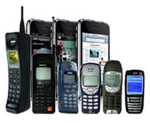
The term wireless communication was introduced in the 19th century and wireless communication technology has developed over the subsequent years. It is one of the most important mediums of transmission of information from one device to other devices. In this technology, the information can be transmitted through the air without requiring any cable or wires or other electronic conductors, by using electromagnetic waves like IR, RF, satellite, etc. In the present days, the wireless communication technology refers to a variety of wireless communication devices and technologies ranging from smart phones to computers, tabs, laptops, Bluetooth Technology, printers. This article gives an overview of wireless communication and types of wireless communications.
Introduction To Wireless Communication
In the present days, wireless communication system has become an essential part of various types of wireless communication devices, that permits user to communicate even from remote operated areas. There are many devices used for wireless communication like mobiles. Cordless telephones, Zigbee wirelss technology, GPS, Wi-Fi, satellite television and wireless computer parts. Current wireless phones include 3 and 4G networks, Bluetooth and Wi-Fi technologies.
Types of Wireless Communication
The different types of wireless communication mainly include, IR wireless communication, satellite communication, broadcast radio, Microwave radio, Bluetooth, Zigbee etc.
Satellite Communication
Satellite communication is one type of self contained wireless communication technology, it is widely spread all over the world to allow users to stay connected almost anywhere on the earth. When the signal (a beam of modulated microwave) is sent near the satellite then, satellite amplifies the signal and sent it back to the antenna receiver which is located on the surface of the earth. Satellite communication contains two main components like the space segment and the ground segment.The ground segment consists of fixed or mobile transmission, reception and ancillary equipment and the space segment, which mainly is the satellite itself.

Infrared Communication
Infrared wireless communication communicates information in a device or systems through IR radiation . IR is electromagnetic energy at a wavelength that is longer than that of red light. It is used for security control, TV remote control and short range communications. In the electromagnetic spectrum, IR radiation lies between microwaves and visible light. So, they can be used as a source of communication
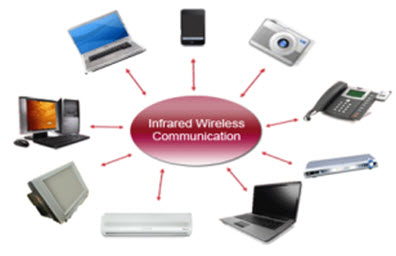
For a successful infrared communication, a photo LED transmitter and a photo diode receptor are required. The LED transmitter transmits the IR signal in the form of non visible light, that is captured and saved by the photoreceptor. So the information between the source and the target is transferred in this way. The source and destination can be mobile phones, TVs, security systems, laptops etc supports wireless communication.
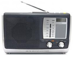
Broadcast Radio
The first wireless communication technology is the open radio communication to seek out widespread use, and it still serves a purpose nowadays. Handy multichannel radios permit a user to speak over short distances, whereas citizen’s band and maritime radios offer communication services for sailors. Ham radio enthusiasts share data and function emergency communication aids throughout disasters with their powerful broadcasting gear, and can even communicate digital information over the radio frequency spectrum.
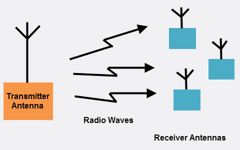
Mostly an audio broadcasting service, radio broadcasts sound through the air as radio waves. Radio uses a transmitter which is used to transmit the data in the form of radio waves to a receiving antenna(Different Types of Antennas). To broadcast common programming, stations are associated with the radio N/W’s. The broadcast happens either in simulcast or syndication or both. Radio broadcasting may be done via cable FM, the net and satellites. A broadcast sends information over long distances at up to two megabits/Sec (AM/FM Radio).
Radio waves are electromagnetic signals, that are transmitted by an antenna.These waves have completely different frequency segments, and you will be ready to obtain an audio signal by changing into a frequency segment.
For example, you can take a radio station. When the RJ says you are listening to 92.7 BIG FM, what he really means is that signals are being broadcasted at a frequency of 92.7megahertz, that successively means the transmitter at the station is periodic at a frequency of 92.700,000 Cycles/second.
When you would like to listen to 92.7 BIG FM, all you have to do is tune the radio to just accept that specific frequency and you will receive perfect audio reception.
Microwave Communication
Microwave wireless communication is an effective type of communication, mainly this transmission uses radio waves, and the wavelengths of radio waves are measured in centimeters. In this communication, the data or information can be transfers using two methods. One is satellite method and another one is terrestrial method.
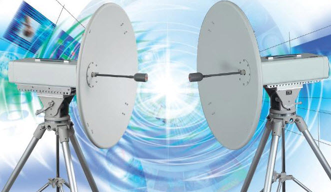
Wherein satellite method, the data can be transmitted though a satellite, that orbit 22,300 miles above the earth. Stations on the earth send and receive data signals from the satellite with a frequency ranging from 11GHz-14GHz and with a transmission speed of 1Mbps to 10Mbps. In terrestrial method, in which two microwave towers with a clear line of sight between them are used, ensuring no obstacles to disrupt the line of sight. So it is used often for the purpose of privacy. The frequency range of the terrestrial system is typically 4GHz-6GHz and with a transmission speed is usually 1Mbps to 10Mbps.
The main disadvantage of microwave signals is, they can be affected by bad weather, especially rain.
Wi-Fi
Wi-Fi is a low power wireless communication, that is used by various electronic devices like smart phones, laptops, etc.In this setup, a router works as a communication hub wirelessly. These networks allow users to connect only within close proximity to a router. WiFi is very common in networking applications which affords portability wirelessly. These networks need to be protected with passwords for the purpose of security, otherwise it will access by others
Mobile Communication Systems
The advancement of mobile networks is enumerated by generations. Many users communicate across a single frequency band through mobile phones. Cellular and cordless phones are two examples of devices which make use of wireless signals. Typically, cell phones have a larger range of networks to provide a coverage.But, Cordless phones have a limited range. Similar to GPS devices, some phones make use of signals from satellites to communicate.
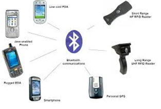
Bluetooth Technology
The main function of the Bluetooth technology is that permits you to connect a various electronic devices wirelessly to a system for the transferring of data.Cell phones are connected to hands free earphones, mouse, wireless keyboard. By using Bluetooth device the information from one device to another device. This technology has various functions and it is used commonly in the wireless communication market.
Advantages of Wireless Communication
- Any data or information can be transmitted faster and with a high speed
- Maintenance and installation is less cost for these networks.
- The internet can be accessed from anywhere wirelessly
- It is very helpful for workers, doctors working in remote areas as they can be in touch with medical centers.
Disadvantages of Wireless Communication
- An unauthorized person can easily capture the wireless signals which spread through the air.
- It is very important to secure the wireless network so that the information cannot be misused by unauthorized users
Applications of Wireless Communication
Applications of wireless communication involve security systems, television remote control, Wi-Fi, Cell phones, wireless power transfer, computer interface devices and various wireless communication based projects.
Wireless Communication Based Projects
Wireless communication based projects mainly include different technologies like Bluetooth, GPS, GSM, RFID and Zigbee projects which are listed below.
- Android Based Smart Phone Used for Induction Motor Control
- Smart Phone Controlled Traffic Signal Override with Density Sensing System
- Arduino based Home Automation
- Phone Controlled Load Management System
- Robotic Vehicle Movement By Cell Phone
- Dialed Telephone Number LED Based Display System
- DTMF based Load Control System
- Dedicated Message Communication Wirelessly between Two Computers
- Wireless Message Communication between Two Computers
- Android based Remotely Programmable Sequential Load Operation
- Remotely Controlled Android based Electronic Notice Board
- Remote Operated Domestic Appliances Control by Android Application
- Remote Password Operated Security Control by Android Applications
- Home Automation by Android Application based Remote Control
Therefore, this is all about Types of wireless communication, these networks are one of the important technologies in the telecommunications market. WiFi, WiMax, Bluetooth, Femtocell, 3G and 4G are some of the most important standards of Wireless technology.
Details about Few Communication Based Projects :
1. Wireless Message Communication between Two Computers :
This project has been developed to ensure communication between computers in any organization using wireless technique. This system can be used at offices to ensure feasible communication between employees using wireless technique.
The 2.4GHz XBee module consisting of both the transmitter and the receiver module is interfaced to the serial port of the computer through a MAX 232 IC used as a level shifter IC. A timer is also used to provide signals to trigger a buzzer alarm in case of reception of message. Thus the person receiving a message can get a alarm tone about arrival of a new message.
2. PC based Electrical Load Control:
This project has been designed to be used at places like theatres, auditoriums where a centralized control system can be used to control the switching of all the electrical appliances. The control can be given through a central computer which gives commands which are accordingly processed by a microcontroller to control the switching of the loads.
The commands are given through the keyboard on the computer. The computer is interfaced to the microcontroller through a level shifter IC. The microcontroller on receiving the commands accordingly provides signals to the relay driver to drive the relay which in turn ensures the switching on or off of the lamp.
3. Password based Remote Controlled Door Opening by Android Application:
This project is designed to build a system wherein the door can be remotely opened or closed based on some password. The commands are sent from a smart phone with Graphical User Interface touch screen based application and accordingly processed to control the opening and closing of the door.
The GUI app on the smart phone with touch screen panel is used to enter the password. This password is send through Bluetooth communication to the receiver part. At the receiver part, the Bluetooth device receives the information and feeds the data to the micro controller. The micro controller matches this data with the one available in the micro controller. If the password matches, the micro controller sends appropriate signals to the motor driver to provide rotation to the motor so as to open the door.
DTMF Based Projects:
- Cell Phone Based DTMF Controlled Garage Door Opening System –
- Display of Dialed Telephone Numbers on Seven Segment Displays –
- Automatic Dialing to any Telephone Using I2C Protocol on Detecting Burglary –
- DTMF Based Load Control System –
- Cell Phone Controlled Robotic Vehicle –
GSM Based Projects:
- Tampered Energy Meter Information Conveyed to Concerned Authority by Wireless Communication – For more information,
- Railway Level Crossing Gate Control through SMS by the Station Master or the Driver – For more information,
- GSM Based Monthly Energy Meter Billing via SMS – For more information,
- Theft Intimation of the Vehicle Over SMS to Owner Who Can Stop the Engine Remotely – For more information,
- Flash Flood Intimation Over GSM Network – For more information,
- Integrated Energy Management System Based on GSM Protocol with Acknowledgement Feature – For more information,
- GSM Based Energy Meter Reading with Load Control – For more information,
- Railway Track Security System – For more information,
- GSM Based Wireless Electronic Notice Board– For more information,
- RFID Based Device Control and Authentication system using PIC Microcontroller – For more information,
- Theft Intimation of Vehicle Over SMS to Owner Who Can Stop the Engine Remotely – For more information,
- GSM Based Energy Meter Reading With Load Control Using PIC Microcontroller – For more information, PC Based Projects:
- PC Based electrical Load Control – For more information,
- SCADA for remote industrial plant –
- Using TV Remote as a Cordless Mouse for the Computer –
- Automatic Survelliance Camera Panning System from PC –
- RF Based Unique Office Communication System –
- PC Controlled Scrolling Message Display for Notice Board –
- Wireless message Communication Between Two Computers –
- Using TV Remote as a Cordless Mouse for the Computer Using PIC Microcontroller –
RF Based Projects:
- Automatic Wireless Health Monitoring System in Hospitals for Patients –
- Secret Code Enabled Secure Communication Using RF Technology –
- RF Controlled Robotic Vehicle With Laser Beam Arrangement –
- Pick N Place With Soft Catching Gripper –
- Fire Fighting Robotic Vehicle War Field Spying Robot with Night Vision Wireless Camera –
- Wireless Power Transfer –
- Speed Synchronization of Multiple Motors in Industries
- RF based Unique Office Communication System–
- Touch Screen Based Home Automation System –
- RF Based Home Automation System –
- Metal Detector Robotic Vehicle –
- Speed Synchronization of Multiple Motors in Industries Using PIC Microcontroller –
RFID Projects:
- RFID Security Access Control System –
- RFID Based Attendance System –
- RFID Based Passport Details –
- Device Control and Authentication using RFID –
Bluetooth Based Projects:
- Remote AC Power Control by Android Application with LCD Display –
- Android Based Remote Programmable Sequential –
- War Field Spying Robot with Night Vision Wireless Camera by Android Applications – Remote Induction Motor Control by Android Application with 7 Segment Display –
- Remote Operated Domestic Appliances Control by Android Application –
- Remote Password Operated Load Control by Android Applications –
- Density Based Auto Traffic Signal Control with Android Based Remote Override –
- Four Quadrant Operation of DC Motor Remotely Controlled by Android Applications –
- Fire Fighting Robot Remotely Operated by Android Applications –
- Pick N Place Robotic Arm and Movement Controlled by Android Wirelessly –
- Metal Detector Robotic Vehicle Operated by Android Application –
- Remote Alignment of 3D Dish Positioning by Android Application –
- Password Based Remote Controlled Door Opening By Android Application –
- Railway Level Crossing Gate Operation Remotely By Android –
- Home Automation by Android Application Based Remote Control –
- Remote Speed Control of DC Motor by Android Applications –
- Android Application Controlled Remote Robot Operation –
- Remotely Controlled Android Based Electronic Notice Board –
XBEE Based Projects
- Wireless Message Communication between Two Computers –
- XBEE Based Remote Monitoring of 3 Parameters on Transformer / Generator Health –
- XBEE Based Remote Monitoring of 3 Parameters on Transformer / Generator Health with Voice Announcement and Wireless PC Interface
Smart Card Based Projects
- Security System Using Smart Card Technology
Wireless Communication Projects for Engineering Students
Wireless communication is defined as sending the information from one point to another point or multiple points without using wires. Wireless communication allows a long range communication, whereas in other communications it is impossible to implement using wires. This communication is used in telecommunication industries and it uses some type of energy to transfer information without using wires over short & long distances. These technologies use radio waves using the radio for short and long distance radio communications. This communication is mainly used in mobile, fixed and portable devices that include PDAs, radio ,cell phones and the applications of wireless communication projects include garage door openers, GPS, wireless computer mice keyboards, satellite vision, headsets, broadcast television, etc.

Wireless Communication Projects based ideas 2015
Wireless communication based projects mainly involve different types of wireless technologies such as GPS, Bluetooth, FID, Zigbee and GSM. For better understanding of these wireless communication technologies we have discussed with projects.
RFID based Ambulance Flashing Light with Beeper
This project is designed to provide a flashing light, which is commonly used in ambulances and emergency vehicles. These flashing lights are located at the top roof of the vehicle to clear the vehicles on the way and also to give an alert to the people to wait and permit it to pass smoothly. The proposed system uses a 8051 families microcontroller to give flashing light at the particular time intervals. A 12v lamp is driven by a power MOSFET in the mode of pulse width modulation. The duty cycle of the pulse width modulation has to be changed as per he type of application. In the future, this project can be developed by using the 230V lamp for better visibility.
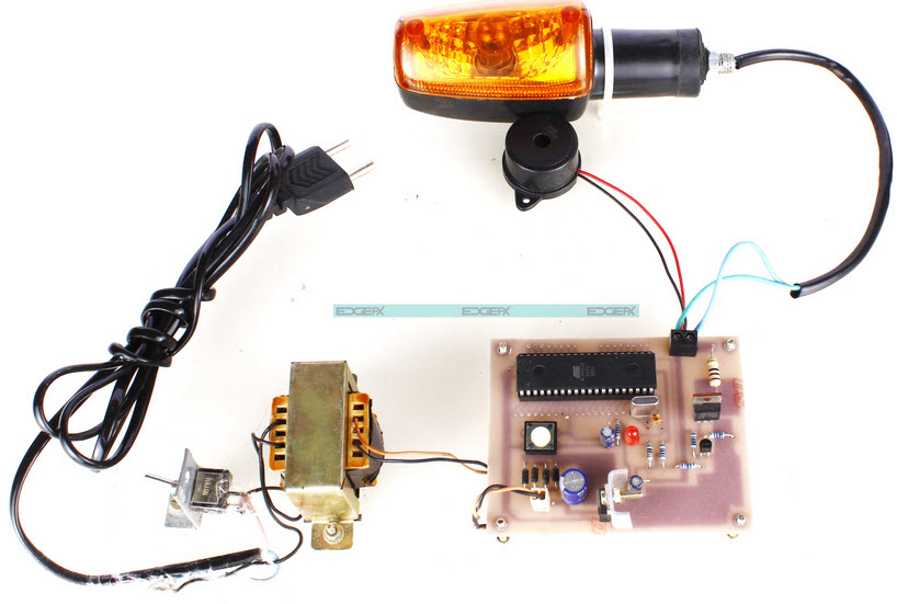
Bluetooth based Garage Door Opening
The main concept of this project is to design a Bluetooth based garage door opening system with a unique password by an any android application. The owner can connect the Bluetooth device with the android application to the system. The proposed system uses a ATMEGA microcontroller to control the garage door open and close by entering the unique password.When the entered password is right, then the door will be open otherwise it will generate a buzzer sound. Further, this project can be enhanced by using an EEPROM so that the password can be changed by the authorized person.
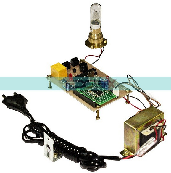
DTMF based Load Control System
This load control system using dual tone multi frequency is used to switch any electrical loads. In various industries, agriculture fields and in the houses different loads are located in large areas so, controlling of loads is a difficult task. To overcome this problem, the proposed system is designed to control the loads remotely by using DTMF technology
A cell phone is connected to a DTMF decoder with this project from its audio o/p outlet for receiving tone instructions. The receiving cell phone codes are changed into digital instructions by using a DTMF Decoder which will recognize the frequency of the key and alter that frequency to its corresponding digital code which is then fed to a microcontroller. According to the instructions sent from the mobile user, the 8051 microcontroller will send indications through a buffer to activate the particular loads by switching the relays ON/OFF. These relays are triggered by a relay driver IC connected to the microcontroller.
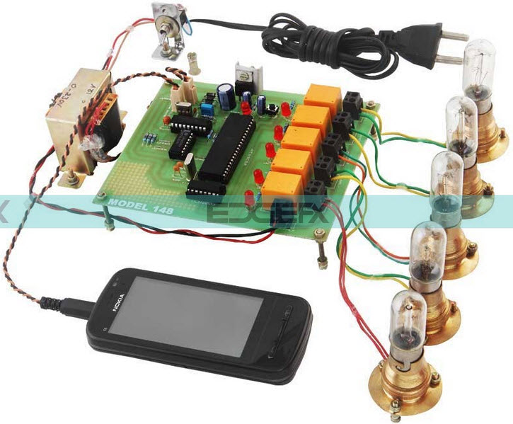
In the future, this project can be developed by using a GSM modem, where the different electrical loads can be controlled by sending an SMS. This will remove the necessity of replying the call for the system to work.
Smart Card Technology based Security System
The main goal of this project is to design a security system using smart card technology to control a device or to access an area. This smart card technology is used in many organizations to access a secure area by using a valid smart card.
At present, human interference was compulsory to observe all these parameters, but using this project no human interference is required. Because this project uses a valid smart cards to operate devices.

The smart card reader is interfaced to an 8051 family micro controller. When the data is read from the smart card data on the micro controller matches, then the message will display on the LCD that the smart card is authorized. A relay is used instantaneously to turn ON a lamp
If an unauthorized card is interleaved in the smart card reader, it displays the message on the LCD display that the card is not authorized and the lamp remains OFF representing that the person is not authorized to entrée the specific area or device. In the future, this project can be developed by adding GSM modem such that any effort of illegal access is made, then an SMS is sent to the concerned department.
Zigbee based Automatic Meter Reading System
The main concept of this project is to design an automatic energy meter reading system using Zigbee. This meter sends unit based pulses which are connected to an Opto coupler that calculates the pulses every time, then the led blinks. As per the ingesting it gives necessary interrupt signal to a micro controller.
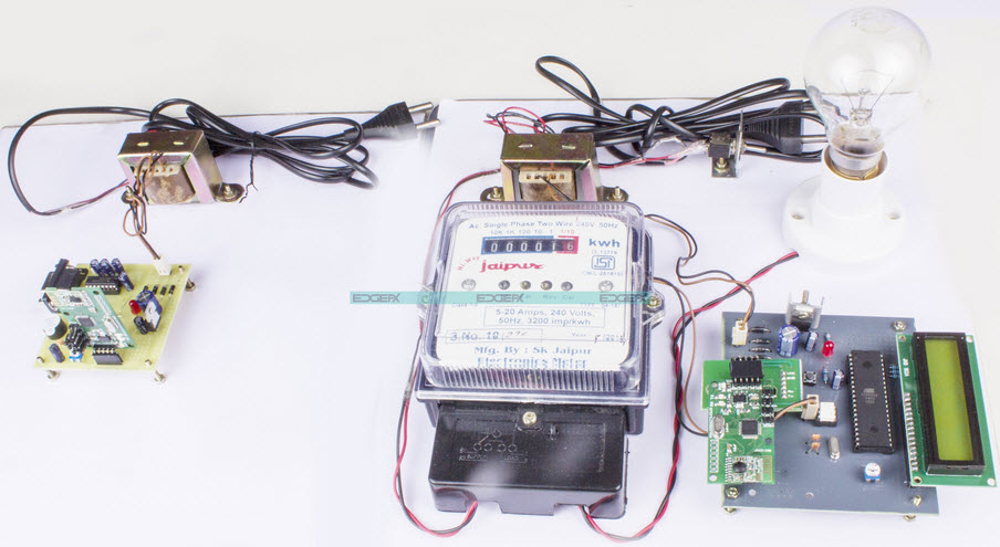
The 8051 micro controller receives the reading from the meter through an Opto-isolator and reading will be displayed on the LCD which is interfaced to the micro controller. The energy meter’s reading is sent wirelessly to the user of the personal computer by a serial data transfer via an 2.4 GHz XBee module attached to the micro controller.
List of Home Automation Projects for Engineering Students
Nowadays automation systems have become widespread in several industries by playing a vital role in dominating many process-related operations. We live in the world of automation wherein most of the systems have become machine-driven, such as industrial automation, automation in homes and alternative business sectors. Home automation systems advancing towards mechanization processes whereby less human efforts are required by the machinery equipments to control numerous systems in homes. It involves automatic controlling of home appliances using completely different technologies and controllers over desktops, laptops good phones or tablets. Automation systems are classified into two types: industrial automation system and home automation systems. Automation systems are classified into two types such as industrial automation system and home automation systems. Home automation systems are are further classified into three types: Power line Based Home Automation Wired or BUS Cable Home Automation Wireless Home Automation. This article discusses about the home automation projects that use Android, DTMF, RF, Arduino and touch screen.
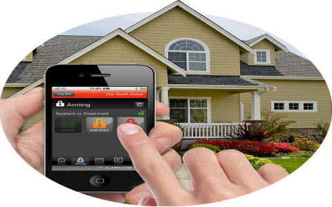
Home Automation Projects
Home automation projects are implemented by using various technologies: Arduino, DTMF, Android, touch screen, etc. The list of home automation projects is given below:
Arduino based Home Automation
The main intention of this project is to design a home automation system using an Arduino board with Bluetooth technology and to control it remotely by any Android operating system based smart phone.
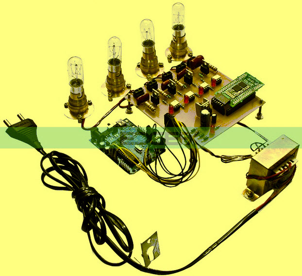
The proposed system uses a Bluetooth module, which is interfaced to the Arduino board at the end of the receiver. At the transmitter end, a GUI (Graphical User Interface) application on the cell phone sends ON/OFF commands to the receiver. By touching the particular location on the GUI, the loads at the receiver end can be turned ON/OFF remotely via., this technology.The loads are operated by an Arduino board through Thyristors and Opto Isolators using TRIACS.
Home Automation by Android Application based Remote Control
The main goal of this project is to design a home automation system with Android application that can be controlled remotely. This proposed system uses an Android OS based smart phone or tablet, upon a graphical user interface based touchscreen operation. In order to achieve this, Android application acts as a transmitter, which sends the ON/OFF commands to the receiver where loads are connected.
By touching a particular remote switch on the transmitter, the loads can be turned ON/OFF via wireless remote. This project uses a microcontroller of the 8051 families. The loads at the receiver end interface to the microcontroller using Opto-Isolators
By touching a particular remote switch on the transmitter, the loads can be turned ON/OFF via wireless remote. This project uses a microcontroller of the 8051 families. The loads at the receiver end interface to the microcontroller using Opto-Isolators

Home Automation Using Digital Control
The main objective of this project is to design a home automation system which is capable of being controlled remotely by using a landline connection. The proposed system controls any home appliances through landline, if someone dials the chosen umber for an exact load. Dialling can be done from the home phone or from any other outside phone. This project is designed without engaging any programmable microcontroller. But, it is based on digital logic using TMF technology, which helps receive the commands from the land phone to develop digital output.

Furthermore, this digital signal is processed to activate switching mechanism via relay driver to turn ON/OFF the loads. It can be used to switch appliances from anywhere. This project gives a new direction to the development of home automation.
RF based Home Automation System
The main aim of this project is to design a home automation system with an RF controlled remote. This project provides a simpler solution with RF technology.
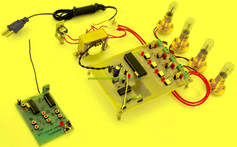
This project uses an RF remote that is interfaced to the microcontroller on transmitter side, which sends On/OFF commands to the receiver where the loads are connected. The loads are interfaced to the microcontroller using Opto-Isolators and TRIACS. In this system, the microcontroller used is from 8051 family. By operating a particular remote switch from the transmitter, the loads can be turned ON/OFF remotely through wireless technology.
Touch Screen based Home Automation System
The main intention of this project is to design a home automation system with touch screen based control panel. In order to achieve this, a touch panel is interfaced to the microcontroller on the transmitter side which sends ON/OFF commands to the receiver where the loads are connected. By touching the particular portion on the touch screen panel, the loads can be turned ON/OFF remotely. Furthermore, this project can be developed by using GSM modem interfaced to the control unit. By using this modem, a user can control home appliances by sending an SMS.
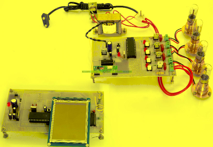
List of Wireless Sensor Networks Project Ideas
A WSN (Wireless Sensor Network) is spatially distributed sensor, that is used to monitor the physical conditions as well as environmental conditions such as sound, temperature, pressure to pass their information through the network to main place. The present networks are bi-directional, also permitting control of sensor activity. The development of these n/w’s is inspired by military applications. The applications of wireless sensor networks mainly involve in consumer and industrial such as health monitoring of a machine, control and monitoring of industrial process and wireless sensor networks projects,. The WSN is made with hundreds and thousands of nodes, where each node is connected with single or multiple sensors.Each node includes various parts like a radio transceiver with an antenna, an electronic circuit, a microcontroller and an energy source.
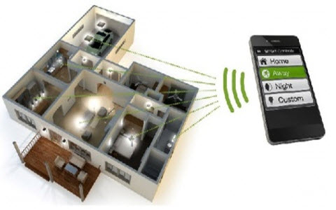
Wireless Sensor Networks Projects
Wireless sensor network projects give an enormous profit to several commercial enterprises such as energy and process improvements, savings of cost, material and energy, labor effort and raises productivity. Some of the wireless sensor networks project ideas for 2015 is discussed below.
WSN based Monitoring of Temperature and Humidity of Soil using Arduino
The main purpose of this project is to design an automatic irrigation system that makes a motor pump to turn ON and OFF by sensing the moisture of the soil. The proper use of an irrigation system in the field of agriculture is very important. The main advantage of using this project is, we can reduce the human involvement
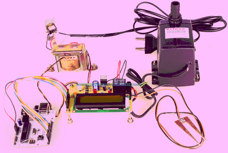
This WSN project uses a preprogrammed Arduino board to receive the i/p signal of changing the moisture condition of soil through a sensing arrangement. The project uses an Arduino board which is programmed to receive the input signal of varying moisture condition of the soil through a sensing arrangement. This process is accomplished by using an operational amplifier which is used as a comparator. This comparator performs as an interface between the microcontroller and the sensing arrangement.
When the microcontroller takes the signal, then it produces an o/p signal to drive a relay for switch ON the water pump. An LCD display is used to display the status of the water pump and the soil, that is interfaced to the microcontroller The sensing arrangement of this project is designed with two metallic stiff rods and the connections of these two rods are given to the control unit.
Furthermore, this project can be developed by interfacing a GSM module. So that we can send an SMS to the concern person regarding the status of the water pump and we can also turn ON/OFF the water pump by sending an SMS.
WSN and GSM Module based Automated Irrigation System
The main concept of this irrigation system is to turn ON/OFF a motor pump by sensing the soil using WSN in the field of agriculture, The status of the soil can be known by sending an SMS using GSM module.
In the agriculture field, the use of irrigation is mandatory. By using this method we can reduce the manpower. This project is designed with a preprogrammed 8051 microcontroller, that receives the signal from the sensor arrangement.
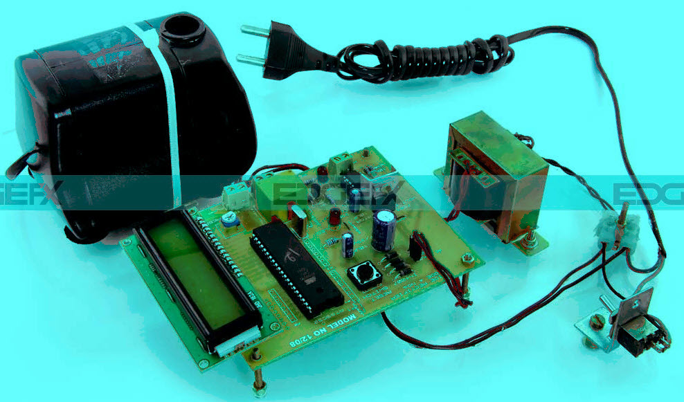
This procedure is attained by using an operational amplifier and it acts as interface b/n the sensing device & the 8051 microcontroller.
When the 8051 microcontroller gets this signal, it makes an output to drive a relay for operating the water pump. Using a GSM modem, it also sends an SMS to the authorized person. An LCD display is used to display the status of water pump ON/OFF condition and the soil. The sensing arrangement is designed with two stiff metallic rods and the connections of these rods are interfaced to the control unit. Furthermore, this project can be developed with Xbee or Bluetooth technology, so that when the water pump turns on or off, the data is sent to a mobile phone.
WSN based Wireless SCADA
In large scale industries, it is impossible to control the various loads. So this project is developed to control the various processes in industries by SCADA. SCADA is a one type of technology, used to monitor the remote areas without human intrusion.This project uses four temperature sensors to form a WSN, that is located in different places. If the temperature sensor increases at the particular point of GUI, then the relay activates to turn ON/OFF the load to maintain the fixed temperature. There are different sensors can be used in SCADA system to control multiple loads. Wireless Network based Wireless SCADA
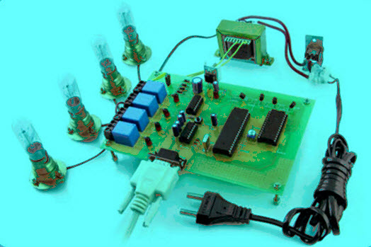
Remote Monitoring System Using XBEE
This XBEE based remote monitoring project is used to protect the transformer by monitoring the three parameters of a generator or transformer like temperature, voltage and current through the sensing devices such as temperature sensor, potential transformer and current transformer to monitor these parameters from a remote location using XBEE. At the transmitter end, three sensors are arranged to make a WSN with a particular range of each parameter. If these three parameters surpass at the fixed limits, then the TX transmits a signal to the receiving end using the XBEE transceiver. Here in this project, a relay is used to switch a warning load and a voice module is used to alert the user.XBEE Based Remote Monitoring System
Thus, this is all about wireless sensor networks projects .
++++++++++++++++++++++++++++++++++++++++++++++++++++
Antenna Modern in Electronic ; RFID , Wireless on CHIP electronic
++++++++++++++++++++++++++++++++++++++++++++++++++++
Komentar ini telah dihapus oleh pengarang.
BalasHapusHello sir, it's a very interesting blog related to Antenna Working principles. Thank you for sharing it will be helpful for engineering students to develop their own academic projects. for some more interesting projects Wireless Sensor Network
BalasHapusWow, that is quite informative. I like this article very much. The content was good. If any of the engineering students are looking for a communication based projects, I found this site and they are providing the best service to the engineering students regarding the projects communication based projects
BalasHapus