
Filters Work
CR Filter Operation.
Figs 8.2.1 and 8.2.2 show two common methods of using C and R together to achieve alterations in AC signals. These CR combinations are used for many purposes in a wide variety of circuits. This section describes their effects when used as filters with sine wave signals of varying frequencies. The same circuits are also used to change the shape of non-sinusoidal waves, and the techniques used are described in Differentiators and Integrators later in this this module.
The High Pass CR Filter

Fig 8.2.1 High Pass CR Filter
The CR circuit illustrated in Fig 8.2.1, when used with sinusoidal signals is called the HIGH PASS FILTER. Its purpose is to allow high frequency sine waves to pass unhindered from its input to its output, but to reduce the amplitude of, (to attenuate) lower frequency signals. A typical application of this circuit would be the correction of frequency response (tone correction) in an audio amplifier.
As described , resistance is constant at any frequency, but the opposition to current flow offered by the capacitor (C) however, is due to capacitive reactance XC, which is greater at low frequencies than at high frequencies.
The reactance of the capacitor (XC) and the resistance of the resistor (R) in fig 8.2.1 act as a potential divider placed across the input, with the output signal taken from the centre of the two components. At low frequencies where XC is much greater than R, the share of the signal voltage across R will be less than that across C and so the output will be attenuated. At higher frequencies, it is arranged, by suitable choice of component values, that the resistance of R will be much greater than the (now low) reactance XC, so the majority of the signal is developed across R, and little or no attenuation will occur.
The Low Pass CR Filter

Fig 8.2.2 Low Pass CR Filter
In Fig 8.2.2 the positions of the resistor and capacitor are reversed, so that at low frequencies the high reactance offered by the capacitor allows all, or almost all of the input signal to be developed as an output voltage across XC. At higher frequencies however, XC becomes much less than R and little of the input signal is now developed across XC. The circuit therefore attenuates the higher frequencies applied to the input and acts as a LOW PASS FILTER.
The band of frequencies attenuated by high and low pass filters depends on the values of the components. The frequency at which attenuation begins or ends can be selected by suitable component choices. In cases of audio tone correction, the resistor may be made variable, allowing a variable amount of bass or treble (low or high frequency) cut. This is the basis of most inexpensive tone controls
High and low pass filters can also be constructed from L and R. In this case the action is the same as for the CR circuit except that the action of XL is the reverse of XC. Therefore in LR filters the position of the components is reversed.
Phase Change in Filters
The above description of high and low pass filters explains how they operate in terms of resistance and reactance. It shows how gain (Vout/Vin) is different at high and low frequencies due to the relative values of XC and R. However this simple explanation does not take the phase relationships between capacitors or inductors, and resistors into account. To accurately calculate voltage values across the components of a filter it is necessary to take phase angles into consideration as well as resistance and reactance. This can be done by using phasor diagrams to calculate the values graphically, or by a branch of algebra using ´complex numbers´ and ´j Notation´. However these calculations can also be done using little more than the Reactance calculations learned in Module 6 and the Impedance Triangle calculations from Module 7.
Problem:
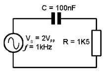
Calculate the peak to peak voltages Vr appearing across R and Vc appearing across C when an AC supply voltage of 2Vpp at 1kHz is applied to the circuit as shown.
Although C and R form a potential divider across Vs it is not possible to calculate these values using the potential divider equation(because phase angles must also be taken into account):

Follow these steps:
1. Find the value of capacitive reactance XC using:


2. Use the Impedance Triangle to find Z (the impedance of the whole circuit).


3. Knowing that the supply voltage Vs is developed across Z, the next step is to calculate the volts per ohm (V/Ω),

Because the volts per ohm will be the same for each component as it is for the circuit impedance, the result from step 3 can now be used to find the voltages across C, and across R.


If required, the Phase angle θ could also be found using trigonometry as described in Phasor Calculations, Module 5.4 (Method 3). To find the angle θ (the phase difference between the supply voltage VS and the supply current, which would be in the same phase as VR) the two voltages already found could be used.

Because circuits containing capacitance (or inductance) in addition to resistance affect the phase relationships of sine wave signals. This allows these same circuits to be used to change the PHASE of signals instead of, or as well as the amplitude.
CR Filter Operation
Fig 8.2.3 and Fig. 8.2.4 demonstrate how phasor diagrams can explain both the amplitude and phase effects of a CR filters. Adjust the frequency slider and notice that it is the input voltage that apparently changes phase, but this is just because the circuit current phasor (and therefore the VR phasor, which is always in phase with the current) is used as the static reference phasor. The thing to remember is that there is a phase change of between 0° and 90° happening between VIN and VOUT, which depends on the frequency of the signal.
Using phasor diagrams to explain the high pass filter shows that:
• In The High pass Filter (Fig. 8.2.3) at low frequencies the output VOUT (VR) is much smaller than VIN (VC) and a phase shift of up to 90° occurs with the output phase leading the input phase.
• At high frequencies there is little or no difference between the relative amplitudes of VOUT (VR) and VIN , and little or no phase shift is taking place. At the corner frequency the phase shift is 45° and below that the Bode plot shows that frequency gain falls off at a steady rate of -20dB per decade.
Fig 8.2.4 similarly demonstrates the action of a CR Low Pass Filter. In this circuit note that VOUT = VC so the output phase lags the input phase by up to about -90°, depending on the input frequency .
Uses for passive filters.
Filters are widely used to give circuits such as amplifiers, oscillators and power supply circuits the required frequency characteristic. Some examples are given below. They use combinations of R, L and C
, Inductors and Capacitors react to changes in frequency in opposite ways. Looking at the circuits for low pass filters, both the LR and CR combinations shown have a similar effect, but notice how the positions of L and C change place compared with R to achieve the same result. The

Fig. 8.1 1 Low pass filters.
Low Pass Filters
Low pass filters are used to remove or attenuate the higher frequencies in circuits such as audio amplifiers; they give the required frequency response to the amplifier circuit. The frequency at which the low pass filter starts to reduce the amplitude of a signal can be made adjustable. This technique can be used in an audio amplifier as a "TONE" or "TREBLE CUT" control. LR low pass filters and CR high pass filters are also used in speaker systems to route appropriate bands of frequencies to different designs of speakers (i.e. ´ Woofers´ for low frequency, and ´Tweeters´ for high frequency reproduction). In this application the combination of high and low pass filters is called a "crossover filter".
Both CR and LC Low pass filters that remove practically ALL frequencies above just a few Hz are used in power supply circuits, where only DC (zero Hz) is required at the output.

Fig. 8.1.2 High pass filters.
High Pass Filters
High pass filters are used to remove or attenuate the lower frequencies in amplifiers, especially audio amplifiers where it may be called a "BASS CUT" circuit. In some cases this also may be made adjustable.
Band pass filters.

Fig.8.1.3 Band pass filters.
Band pass filters allow only a required band of frequencies to pass, while rejecting signals at all frequencies above and below this band. This particular design is called a T filter because of the way the components are drawn in a schematic diagram. The T filter consists of three elements, two series−connected LC circuits between input and output, which form a low impedance path to signals of the required frequency, but have a high impedance to all other frequencies.
Additionally, a parallel LC circuit is connected between the signal path (at the junction of the two series circuits) and ground to form a high impedance at the required frequency, and a low impedance at all others. Because this basic design forms only one stage of filtering it is also called a ´first order´ filter. Although it can have a reasonably narrow pass band, if sharper cut off is required, a second filter may be added at the output of the first filter, to form a ´second order´ filter.
Band stop filters.

Fig.8.1.4 Band stop filters.
These filters have the opposite effect to band pass filters, there are two parallel LC circuits in the signal path to form a high impedance at the unwanted signal frequency, and a series circuit forming a low impedance path to ground at the same frequency, to add to the rejection. Band stop filters may be found (often in combination with band pass filters) in the intermediate frequency (IF) amplifiers of older radio and TV receivers, where they help produce the frequency response curves of quite complex shapes needed for the correct reception of both sound and picture signals. Combinations of band stop and band pass filters, as well as tuned transformers in these circuits, require careful frequency adjustment.
I.F. Transformers.

Fig.8.1.5 I.F. Transformer
These are small transformers, found in older in radio and TV equipment to pass a band of radio frequencies from one stage of the intermediate frequency (IF) amplifiers, to the next. They have an adjustable core of compressed iron dust (Ferrite). The core is screwed into, or out of the windings forming a variable inductor.
This variable inductor, together with a fixed capacitor ´tunes´ the transformer to the correct frequency. In older TV receivers a number of individually tuned IF transformers and adjustable filter circuits were used to obtain a special shape of pass band to pass both the sound and vision signals. This practice has largely been replaced in modern receivers by packaged filters and SAW Filters.
Packaged Filters.
There are thousands of filters listed in component catalogues, some using combinations of L C and R, but many making use of ceramic and crystal piezo-electric materials. These produce an a.c. electric voltage when they are mechanically vibrated, and they also vibrate when an a.c. voltage is applied to them. They are manufactured to resonate (vibrate) only at one particular, and very accurately controlled frequency and are used in applications such as band pass and band stop filters where a very narrow pass band is required. Similar designs (crystal resonators) are used in oscillators to control the frequency they produce, with great accuracy. One packaged filter in TV receivers can replace several conventional IF transformers and LC filters. Because they require no adjustment, the manufacture of RF (radio frequency) products such as radio, TV, mobile phones etc. is simplified and consequently lower in price. Sometimes however, packaged filters will be found to have an accompanying LC filter to reject frequencies at harmonics of their design frequency, which ceramic and crystal filters may fail to eliminate.
SAW Filters

Fig.8.1.6 SAW Filters.
The illustration (right) shows a Surface Acoustic Wave (SAW) IF (intermediate frequency) filter ON A CIRCUIT BOARD FROM A PAL TV. SAW filters can be manufactured to either a very narrow pass band, or a very wide band with a complex (pass and stop) response to several different frequencies. They can produce several different signals of specific amplitudes at their output. Special TV types replace several LC tuned filters in both analogue and digital TVs with a single filter. They work by creating acoustic waves on the surface of a crystal or tantalum substrate, produced by a pattern of electrodes arranged as parallel lines on the surface of the chip. The waves created by one set of transducers is sensed by another set of transducers designed to accept certain wavelengths and reject others. Saw filters may be found in many types of electronic equipment and have response curves tailored to the requirements of specific types of product, including communications devices, automotive and industrial applications, where they are used for selecting or rejecting particular bands of frequencies.
Ceramic Filters

Fig.8.1.6 Ceramic Filter
& its Circuit Symbol
Ceramic filters are available in a number of specific frequencies, and use a tiny block of piezo electric ceramic material that will mechanically vibrate when an a.c. signal of the correct frequency is applied to an input transducer attached to the block. This vibration is converted back into an electrical signal by an output transducer, so only signals of a limited range around the natural resonating frequency of the piezo electric block will pass through the filter. Ceramic filters tend to be cheaper, more robust and more accurate than traditional LC filters for applications at radio frequencies. They are supplied in different forms including surface mount types, and the encapsulated three pin package .
Showing Phase Shift and Attenuation
When considering the operation of filters, the two most important characteristics are:
- • The FREQUENCY RESPONSE, which illustrates those frequencies that will, and will not be attenuated.
- •The PHASE SHIFT created by the filter over its operating range of frequencies.
Bode Plots show both of these characteristics on a shared frequency scale making a comparison between the gain of the filter and the phase shift simple and accurate.
Frequency is plotted on the horizontal axis using a logarithmic scale, on which every equal division represents ten times the frequency scale of the previous division, this allows for a much wider range of frequency to be displayed on the graph than would be possible using a simple linear scale. Because the frequency scale increases in "Decades" (multiples of x10) it is also a convenient way to show the slope of the gain graph, which can be said to fall at 20dB per decade.
The vertical axis of the gain graph is marked off in equal divisions, but uses a logarithmic unit, the decibel (dB) to show the gain, which with simple passive filters is always unity, or a gain ratio of 1, (which corresponds to 0dB on the logarithimic Decibel scale) or less. The dB units therefore have negative values indicating that the output of the filter is always less than the input, (a gain of less than 1). The upper section of the vertical axis is plotted in degrees of phase change, varying between 0 and 90° or sometimes between −90° and +90°

Fig 8.3.1 Bode Plot for a Low Pass Filter.
A Bode plot for a low pass filter is shown in Fig 8.3.1. Note the point called the corner frequency. This is the approximate point at which the filter becomes effective. Frequencies below this point are unaffected by the filter, while above the corner frequency, attenuation of the signal increases at a constant rate of 6dB per octave. This means that the signal output voltage is halved (−6dB) for each doubling (an octave) of the input frequency.
Alternatively the same fall off in gain may be labelled as −20dB per decade, which means that voltage gain falls by ten times (to 1/10 of its previous value) for every decade (tenfold) increase in frequency. The fall off in gain of a filter is quite linear beginning from the corner frequency (also called the cut off frequency). I.e. if the voltage gain of a low pass filter is 1 at a frequency of 1kHz, it will be 0.1 at 10kHz. The linear fall off in gain is common to both high and low pass filters, it is just the direction of the fall, increasing or decreasing with frequency, that is different.
The corner (or cut off) frequency (ƒC) is where the active part of the gain plot begins, and the gain has fallen by −3dB. The phase lag of the output signal in a low pass filter (or phase lead in a high pass filter) is at 45°, exactly half way between its two possible extremes of 0° and 90° The corner frequency may be calculated for any two values of C and R using the formula:

For LR filters the formula is:

Note that the corner frequency is that point where two straight lines representing the two sections of the graph either side of ƒC would intersect. The actual curve makes a smooth transition between the horizontal and sloping sections of the graph and the gain of the filter is therefore -3dB at ƒC
A simple RC network such as the high pass filter illustrated in Fig. 8.4.1, when used with non sinusoidal waves produces a change in wave shape at its output. With a sine wave input, only the amplitude and phase of the wave change. However, if the input wave is a complex wave, such as a square or triangular wave, the effect of these simple circuits appears to be quite different.
Differentiation
Fig.8.4.1 The Differentiator Circuit

Fig 8.4.2 Differentiation.
The circuit is called a DIFFERENTIATOR because its effect is very similar to the mathematical function of differentiation, which means (mathematically) finding a value that depends on the RATE OF CHANGE of some quantity. The output wave of a DIFFERENTIATOR CIRCUIT is ideally a graph of the rate of change of the voltage at its input. Fig. 8.4.2 shows how the output of a differentiator relates to the rate of change of its input, and that actually the actions of the high pass filter and the differentiator are the same.
Because the differentiator output is effectively a graph showing the rate of change of the input, whenever the input is changing rapidly, a large voltage is produced at the output. The polarity of the output voltage depends on whether the input is changing in a positive or a negative DIRECTION.
Sine Waves
A graph of the rate of change of a sine wave is another sine wave that has undergone a 90° phase shift (with the output wave leading the input wave).
Square Waves
The square wave input and output in Fig 8.4.2 shows the ideal differentiator action of a high pass filter. The output wave is now nothing like the input wave, but consists of narrow positive and negative spikes. The positive spike coincides in time with the rising edge of the input square wave. The negative spike of the output wave coincides with the falling, or negative going (towards zero volts) edge of the square wave. Notice that the DC level of the wave is also changed by the differentiator. The output wave now has both positive and negative half cycles above and below a centre line of zero volts, due to the dc blocking effect of the capacitor.
Triangular Waves
A triangular wave has a steady positive going rate of change as the input voltage rises, so produces a steady positive voltage at the output. As the input voltage falls at a steady rate of change, a steady negative voltage appears at the output. The graph of the rate of change of a triangular wave is therefore a square wave. Wave shaping using a simple high pass filter or differentiator is a very widely used technique, used in many different electronic circuits.
Practical Differentiation

Fig 8.4.3 Practical Differentiation.
Although the ideal situation is shown in Fig. 8.4.2, how closely the output resembles perfect differentiation depends on the frequency (and therefore periodic time) of the input wave and the time constant of the components used, as shown in Fig. 8.4.3. The high pass filter works as a differentiator when the input is:
a. A non-sinusoidal wave.
b. The time constant(T) of the input wave is much greater (longer duration) than the time constant(CR) of the circuit (T>>CR), i.e. at relatively low frequencies.
When T is less than or equal to CR (T<=CR) the output wave shape will be less than an ideally differentiated wave shape, being more or less like the waveforms shown in the bottom row of Fig. 8.4.3.
Although passive (with no amplification) differentiators are cheap and efficient, where it is necessary to control the amplitude of the output, active differentiators using op-amps.
The Integrator Circuit
Fig. 8.5.1 The Integrator (also low-pass filter) Circuit
Integration is used extensively in electronics to convert square waves into triangular waveforms, in doing this it has the opposite effect to differentiation . The shape of the input wave of an integrator circuit in this case will be a graph of the rate of change of the output wave as can be seen by comparing the square wave input and output waveforms in Fig. 8.5.2. Notice that the integrator circuit (shown in Fig. 8.5.1) .
Integrator Action with a Sine Wave Input

Fig. 8.5.2 Integrator Action
If the input is a sine wave, the circuit does not act as an integrator, but as a simple low pass filter (LPF) where the amplitude of the output wave is reduced, and its phase relative to the input wave is shifted so that it lags by up to -90° dependant on the frequency of the wave and the CR time constant of the circuit, as described in Filters & Wave shaping Module 8.2
The low pass filter circuit is therefore called an integrator only when:
a. The input wave is a square wave.
b. The periodic time(T) of the input wave is much shorter than the circuit time constant(CR) i.e.(T<=CR).
Provided that these conditions are met, then the action of the integrator is opposite to that of the differentiator circuit described in Filters and Wave shaping Module 8.4.
Integration of a Square Wave
With a square wave input and the correct relationship between the periodic time of the wave and the time constant of the circuit, Fig 8.5.2 shows that integration takes place. The output is now (considering the waveforms as simple graphs), a graph of the changing area beneath the input wave. The integrator has converted the square wave input to a triangular wave at the output, the slope of this wave describes the increase in area beneath the square wave (moving from left to right). For the circuit to act effectively as an integrator, the periodic time of the wave must be similar to, or shorter than the circuit time constant i.e. (T<=CR). The higher the frequency of the input wave for a particular time constant, the better the shape of the output wave will be, but the smaller its amplitude.
At lower frequencies, where the periodic time T of the wave is much longer than the time constant of the circuit CR (T>>CR), some change in wave shape does occur, but the output does not conform to the definition of an integrator; the circuit has just rounded the rapid vertical transitions of the square wave. The output at these low frequencies is not a graph of the changing area beneath the input wave, the circuit is acting as a low pass filter and removing the high frequency components of the square wave that were responsible for the rapid vertical changes at each half cycle.
Action on a Triangular Wave
When the input to the integrator circuit is a triangular wave, the output seems to become a sine wave. Remember however, that the integrator circuit is also a low pass filter that has the effect of removing the higher frequency harmonics present in the complex (triangular) wave at its input, leaving just the fundamental (sine wave) and possibly a few lower frequency harmonics. At low frequencies, the output from the integrator circuit is therefore a rounded form of the triangular input wave.
The main purpose of a passive CR integrator is to produce a good triangular wave shape from a square wave input, which it can do very well and at very low cost (only two components are needed) although the output will be reduced in amplitude. Any lack of amplitude may be overcome by combining the passive CR circuits described in this module with an op-amp to create an active filter, differentiator or integrator
XXX . XXX Minimizing LED Flicker in Lighting Applications
Replacing traditional incandescent lights with efficient, cool, and long-lasting LEDs is a good idea. But like all good ideas, the implementation is a little harder than coming up with the notion in the first place.
Although LED lights can be supplied with driver circuitry to allow them to be connected to the existing domestic AC power supply, there is a risk that flickering could occur as a result of voltage ripple at the supply’s output. Flickering occurs with most lighting, and some consumers complain that the effect makes them feel uncomfortable or even ill.
LED and luminaire manufacturers are keen to get to the root of the problem, because should solid-state lighting get a reputation for flickering – however undeserved – convincing consumers to move away from traditional lights will become more difficult.
This article investigates the cause of flickering, describes why it is a particular problem for LEDs, and explains how engineering administrative and standards-making bodies are trying to quantify the phenomenon for test houses and the LED, driver chip, and luminaire makers. The article will then describe some recent product introductions from major silicon vendors that claim to offer a cost-effective way of implementing flicker-free LED lighting.
The effect of flicker
According to studies about 1 in 4,000 people are highly susceptible to flashing lights cycling in the 3 to 70 Hz range. Such obvious flickering can trigger ailments as serious as epileptic seizures. Less well known is the fact that long-term exposure to higher frequency (unintentional) flickering (in the 70 to 160 Hz range) can also cause malaise, headaches, and visual impairment.
Unfortunately, unless a person is in natural daylight, they are likely to be exposed to this higher frequency flickering, because all mains-powered light sources, whether incandescent, halogen, fluorescent or LED, are subject to flickering. The source is the AC component of the power supply and the frequency of the flickering is typically either equal to the mains frequency (usually 50 or 60 Hz) or double the mains frequency.
Tests show that humans find it difficult to directly sense light flickering at these higher frequencies, but that seems to hardly matter. Scientists have conducted research that indicates the human retina is able to resolve light flickering at 100 to 150 Hz, even if the subject is not aware of it, leading to the conclusion that the brain may well be reacting.
The insidious effects of this so-called imperceptible flickering in the 100 to 150 Hz range are not just a function of frequency; physical and physiological factors also play a big part. For example, bright light is worse than dim, and the difference between “bright” and “dark” parts of the lighting pattern are important (a light that goes completely dark during the “off” part of the cycle is worse than one which only partially dims). Red light and alternating red and blue can be particularly troublesome, and the position of the light source on the retina is important, as light sensed by the center is worse than that falling on the periphery.
Some researchers even claim the retina can sense flickering up to 200 Hz, but tests have shown that above 160 Hz the health effects of flickering are negligible.¹
Defining flicker
Until recently, lighting engineers have been relatively unconcerned by the effects of imperceptible flicker. However, the tightening of health and safety rules, better research, and increasing complaints from staff working in offices illuminated by ubiquitous fluorescent tubes have led to calls for action.
But without a definition for flicker, who’s to say whether one light source is better than another? The Illuminating Engineering Society of North America (IESNA) has addressed this challenge and come up with a definition of “percent flicker” and “flicker index” in the ninth edition of The IESNA Lighting Handbook. Figure 1 shows how the metrics are defined.

Percent flicker is a relative measure of the cyclic variation in output of a light source (i.e., percent modulation). This is also sometimes referred to as the “modulation index.”
From the figure: Percent flicker = 100 x (A – B)/(A + B)
Flicker index is a “reliable relative measure of the cyclic variation in output of various sources at a given power frequency. It takes into account the waveform of the light output as well as its amplitude,” according to the handbook. The flicker index assumes values from 0 to 1.0, with 0 for steady light output. Higher values indicate an increased possibility of noticeable lamp flicker, as well as stroboscopic effect.
Again, from the figure: Flicker index = Area 1/Area 1 + Area 2
The problem with LEDs
The physical characteristics of LEDs determine that they must be powered in a different way to other light sources (see the TechZone article “Understanding the Cause of Fading in High-Brightness LEDs”).
LEDs are, as the name states, a form of diode. In normal operation, a constant forward voltage of sufficient magnitude (typically with the LED in series with a resistor) such that the device is operating in its conduction region, is applied. Forward voltages for commercial high brightness devices are typically in the 3 to 4.5 V range. The relationship between forward voltage (VF) and forward current (IF) is important because the current determines the relative luminous flux (essentially the brightness) of the LED.
The device manufacturer will recommend a tight operating range for an LED that is typically a compromise between brightness and efficacy.
Figures 2a and b illustrate the voltage vs. current and current vs. relative luminous flux for a Cree XLamp ML-B LED. Variation in the forward voltage will affect the forward current and hence the luminous flux.

Powering an LED chip from an AC source requires a regulator to step-down the 110 to 115 or 230 to 240 V, 50 or 60 Hz mains supply used by most countries to the modest voltage and current requirements of LEDs. Note that luminaires typically use six to eight LED chips per fixture, so the power requirement for each unit is higher than that for a single LED.
One basic form of LED driver comprises a full wave rectifier (Figure 3) connected to an LED string with a resistor in series to limit the current. This approach modulates the LEDs at twice the AC frequency (i.e., 100 to 120 Hz). Because the luminous intensity is proportional to the current, the LED flickers at this rate (Figure 4).


All light sources that ultimately derive their power from the AC mains are likely to flicker. But LEDs are particularly bad because the flicker index (or depth of modulation) is typically worse than conventional light sources.
This is because LEDs react particularly quickly to current variations. At 120 Hz, both the LED itself and its white-light-emitting phosphor have plenty of time to completely stop producing photons during the “off” part of the waveform. In contrast, conventional light sources, particularly incandescent and halogen types, have “inertia”. This means that even during the “off” part of the cycle, they still emit some photons.
Table 1 summarizes the percent flicker and flicker index of various light sources including LEDs driven from both DC and AC sources.² (The “Min,” “Max,” and “Ave” columns summarize the relative intensity of each source.)
As noted above, in addition to the frequency, the flicker index has a significant effect on how the light makes people feel. Higher flicker index tends to be more noticeable and hence is potentially more detrimental.
Improved LED drivers
Most contemporary LED drivers are a little more sophisticated than the simple example given in Figure 3, with high-frequency switching power supplies being a popular choice because of their efficiency. Input and output filtering utilized by the switching supplies dramatically reduces the AC component of the mains supply at the output, but some ripple is unavoidable. Some units are worse than others, so the engineer is advised to choose their LED driver carefully.
While switching LED power supplies help reduce the flicker index by attenuating the AC component of their output, the frequency of flickering, at twice the mains frequency, is unaffected and remains right in the range that has been identified by researchers as a problem for humans.
The influential U.S. Environmental Protection Agency (EPA) has attempted to address the problem by recommending that the operational frequency for LEDs be raised to 150 Hz. The organization’s ENERGY STAR specifications – to which makers must adhere is they want to qualify for commercially advantageous ENERGY STAR certification - include one aimed at flicker.
In 2009, the specification referring to flicker was changed to stipulate a minimum LED operating frequency of 150 Hz, up from 120 Hz in the previous version of the spec. LED and semiconductor manufacturers were less than impressed because changing their products to suit the new frequency would have been very expensive.
In a letter to interested parties dated March 2010,³ the EPA relented and changed the specification back to the original 120 Hz, where it remains to this day.
That said, there are many LED drivers on the market that connect directly to a mains supply yet claim to produce “flicker-free” power. Cirrus Logic, for example, has recently released its CS161x LED Driver family (CS1610-FSZ, CS1611-FSZ). The chips are suitable for use with 100 to 120 VAC and 220 to 240 VAC line voltages and boast the added advantage of maintaining the flicker-free performance even when used with legacy dimming switches (which often introduce complications for LED drivers that compromise flicker index).
CUI Inc. also offers a constant current driver that offers flicker-free performance at full brightness and when used with traditional dimming switches, called the V-Infinity VLED15 (Figure 5). The module is available in two versions, one for 115 VAC inputs and the other for 230 VAC inputs.

Another option is ROHM Semiconductor’s BP5843A. This is an 11-pin SIP module that can be used to power several high brightness LEDs in serial or parallel from a 113 to 170 VAC supply. The module features a low peak-to-peak output voltage ripple that helps ensure flicker-free LED power.
In summary
Lighting engineers designing LED luminaires can point to many advantages for their light sources, such as efficacy, longevity, and robustness. However, they do need to be aware of the potential adverse reaction to their products that could be prompted if the consumer feels uncomfortable under solid-state lights.
Although the flicker may be imperceptible, it could still be a problem. For example, workers in offices illuminated by flickering fluorescent tubes have been quick to point to “sick building syndrome” as a reason for higher-than-average absence rates. There is no direct evidence that flicker causes the malaise, but recent research suggests there is a good chance it is one of the causes.
Accordingly, designing LED lighting with flicker reduction in mind is a good idea. Choose good quality high frequency switching LED drivers, as these will minimize the AC component in the voltage and current ripples at the output – which in turn will limit the modulation depth of the LEDs’ flicker. And, although further research is needed to confirm the suggestion, it is also a good idea to keep a look out for LED drivers that convert the AC component in the output ripple to 150 Hz or higher, because early indication are that at this frequency, any flicker has a negligible effect on health.
Although LED lights can be supplied with driver circuitry to allow them to be connected to the existing domestic AC power supply, there is a risk that flickering could occur as a result of voltage ripple at the supply’s output. Flickering occurs with most lighting, and some consumers complain that the effect makes them feel uncomfortable or even ill.
LED and luminaire manufacturers are keen to get to the root of the problem, because should solid-state lighting get a reputation for flickering – however undeserved – convincing consumers to move away from traditional lights will become more difficult.
This article investigates the cause of flickering, describes why it is a particular problem for LEDs, and explains how engineering administrative and standards-making bodies are trying to quantify the phenomenon for test houses and the LED, driver chip, and luminaire makers. The article will then describe some recent product introductions from major silicon vendors that claim to offer a cost-effective way of implementing flicker-free LED lighting.
The effect of flicker
According to studies about 1 in 4,000 people are highly susceptible to flashing lights cycling in the 3 to 70 Hz range. Such obvious flickering can trigger ailments as serious as epileptic seizures. Less well known is the fact that long-term exposure to higher frequency (unintentional) flickering (in the 70 to 160 Hz range) can also cause malaise, headaches, and visual impairment.
Unfortunately, unless a person is in natural daylight, they are likely to be exposed to this higher frequency flickering, because all mains-powered light sources, whether incandescent, halogen, fluorescent or LED, are subject to flickering. The source is the AC component of the power supply and the frequency of the flickering is typically either equal to the mains frequency (usually 50 or 60 Hz) or double the mains frequency.
Tests show that humans find it difficult to directly sense light flickering at these higher frequencies, but that seems to hardly matter. Scientists have conducted research that indicates the human retina is able to resolve light flickering at 100 to 150 Hz, even if the subject is not aware of it, leading to the conclusion that the brain may well be reacting.
The insidious effects of this so-called imperceptible flickering in the 100 to 150 Hz range are not just a function of frequency; physical and physiological factors also play a big part. For example, bright light is worse than dim, and the difference between “bright” and “dark” parts of the lighting pattern are important (a light that goes completely dark during the “off” part of the cycle is worse than one which only partially dims). Red light and alternating red and blue can be particularly troublesome, and the position of the light source on the retina is important, as light sensed by the center is worse than that falling on the periphery.
Some researchers even claim the retina can sense flickering up to 200 Hz, but tests have shown that above 160 Hz the health effects of flickering are negligible.¹
Defining flicker
Until recently, lighting engineers have been relatively unconcerned by the effects of imperceptible flicker. However, the tightening of health and safety rules, better research, and increasing complaints from staff working in offices illuminated by ubiquitous fluorescent tubes have led to calls for action.
But without a definition for flicker, who’s to say whether one light source is better than another? The Illuminating Engineering Society of North America (IESNA) has addressed this challenge and come up with a definition of “percent flicker” and “flicker index” in the ninth edition of The IESNA Lighting Handbook. Figure 1 shows how the metrics are defined.
Figure 1: Schematic of light output trace used to define percent flicker and flicker index.
Percent flicker is a relative measure of the cyclic variation in output of a light source (i.e., percent modulation). This is also sometimes referred to as the “modulation index.”
From the figure: Percent flicker = 100 x (A – B)/(A + B)
Flicker index is a “reliable relative measure of the cyclic variation in output of various sources at a given power frequency. It takes into account the waveform of the light output as well as its amplitude,” according to the handbook. The flicker index assumes values from 0 to 1.0, with 0 for steady light output. Higher values indicate an increased possibility of noticeable lamp flicker, as well as stroboscopic effect.
Again, from the figure: Flicker index = Area 1/Area 1 + Area 2
The problem with LEDs
The physical characteristics of LEDs determine that they must be powered in a different way to other light sources (see the TechZone article “Understanding the Cause of Fading in High-Brightness LEDs”).
LEDs are, as the name states, a form of diode. In normal operation, a constant forward voltage of sufficient magnitude (typically with the LED in series with a resistor) such that the device is operating in its conduction region, is applied. Forward voltages for commercial high brightness devices are typically in the 3 to 4.5 V range. The relationship between forward voltage (VF) and forward current (IF) is important because the current determines the relative luminous flux (essentially the brightness) of the LED.
The device manufacturer will recommend a tight operating range for an LED that is typically a compromise between brightness and efficacy.
Figures 2a and b illustrate the voltage vs. current and current vs. relative luminous flux for a Cree XLamp ML-B LED. Variation in the forward voltage will affect the forward current and hence the luminous flux.
Figure 2a and 2b: Forward voltage vs. forward current and forward current vs. relative luminous flux for a Cree XLamp ML-B LED.
Powering an LED chip from an AC source requires a regulator to step-down the 110 to 115 or 230 to 240 V, 50 or 60 Hz mains supply used by most countries to the modest voltage and current requirements of LEDs. Note that luminaires typically use six to eight LED chips per fixture, so the power requirement for each unit is higher than that for a single LED.
One basic form of LED driver comprises a full wave rectifier (Figure 3) connected to an LED string with a resistor in series to limit the current. This approach modulates the LEDs at twice the AC frequency (i.e., 100 to 120 Hz). Because the luminous intensity is proportional to the current, the LED flickers at this rate (Figure 4).
Figure 3: Simple LED full wave rectifier driver.
Figure 4: Output from the LEDs in Figure 3. The lights flicker at twice the mains frequency.
All light sources that ultimately derive their power from the AC mains are likely to flicker. But LEDs are particularly bad because the flicker index (or depth of modulation) is typically worse than conventional light sources.
This is because LEDs react particularly quickly to current variations. At 120 Hz, both the LED itself and its white-light-emitting phosphor have plenty of time to completely stop producing photons during the “off” part of the waveform. In contrast, conventional light sources, particularly incandescent and halogen types, have “inertia”. This means that even during the “off” part of the cycle, they still emit some photons.
Table 1 summarizes the percent flicker and flicker index of various light sources including LEDs driven from both DC and AC sources.² (The “Min,” “Max,” and “Ave” columns summarize the relative intensity of each source.)
As noted above, in addition to the frequency, the flicker index has a significant effect on how the light makes people feel. Higher flicker index tends to be more noticeable and hence is potentially more detrimental.
| Max | Min | Ave | % Flicker | Flicker Index | |
| Incandescent | 12.180 | 10.745 | 11.460 | 6.2594 | 0.0194 |
| 100 W MH | 9.1472 | 3.2066 | 6.5147 | 48.088 | 0.1398 |
| T12 Magnetic | 9.6281 | 4.6256 | 7.1565 | 35.096 | 0.0897 |
| T5HO Elec | 10.52 | 9.960 | 10.20 | 2.734 | 0.0036 |
| LED at DC | 43.4 | 41.0 | 42.2 | 2.84 | 0.0037 |
| LED w/ Flicker | 15.996 | 0.0555 | 6.3026 | 99.309 | 0.4498 |
Table 1: Summary of percent flicker and flicker index for light sources. Higher flicker index is more noticeable to the human eye.
Improved LED drivers
Most contemporary LED drivers are a little more sophisticated than the simple example given in Figure 3, with high-frequency switching power supplies being a popular choice because of their efficiency. Input and output filtering utilized by the switching supplies dramatically reduces the AC component of the mains supply at the output, but some ripple is unavoidable. Some units are worse than others, so the engineer is advised to choose their LED driver carefully.
While switching LED power supplies help reduce the flicker index by attenuating the AC component of their output, the frequency of flickering, at twice the mains frequency, is unaffected and remains right in the range that has been identified by researchers as a problem for humans.
The influential U.S. Environmental Protection Agency (EPA) has attempted to address the problem by recommending that the operational frequency for LEDs be raised to 150 Hz. The organization’s ENERGY STAR specifications – to which makers must adhere is they want to qualify for commercially advantageous ENERGY STAR certification - include one aimed at flicker.
In 2009, the specification referring to flicker was changed to stipulate a minimum LED operating frequency of 150 Hz, up from 120 Hz in the previous version of the spec. LED and semiconductor manufacturers were less than impressed because changing their products to suit the new frequency would have been very expensive.
In a letter to interested parties dated March 2010,³ the EPA relented and changed the specification back to the original 120 Hz, where it remains to this day.
That said, there are many LED drivers on the market that connect directly to a mains supply yet claim to produce “flicker-free” power. Cirrus Logic, for example, has recently released its CS161x LED Driver family (CS1610-FSZ, CS1611-FSZ). The chips are suitable for use with 100 to 120 VAC and 220 to 240 VAC line voltages and boast the added advantage of maintaining the flicker-free performance even when used with legacy dimming switches (which often introduce complications for LED drivers that compromise flicker index).
CUI Inc. also offers a constant current driver that offers flicker-free performance at full brightness and when used with traditional dimming switches, called the V-Infinity VLED15 (Figure 5). The module is available in two versions, one for 115 VAC inputs and the other for 230 VAC inputs.
Figure 5: CUI Inc’s VLED15 offer flicker-free LED power even with legacy dimming switches.
Another option is ROHM Semiconductor’s BP5843A. This is an 11-pin SIP module that can be used to power several high brightness LEDs in serial or parallel from a 113 to 170 VAC supply. The module features a low peak-to-peak output voltage ripple that helps ensure flicker-free LED power.
In summary
Lighting engineers designing LED luminaires can point to many advantages for their light sources, such as efficacy, longevity, and robustness. However, they do need to be aware of the potential adverse reaction to their products that could be prompted if the consumer feels uncomfortable under solid-state lights.
Although the flicker may be imperceptible, it could still be a problem. For example, workers in offices illuminated by flickering fluorescent tubes have been quick to point to “sick building syndrome” as a reason for higher-than-average absence rates. There is no direct evidence that flicker causes the malaise, but recent research suggests there is a good chance it is one of the causes.
Accordingly, designing LED lighting with flicker reduction in mind is a good idea. Choose good quality high frequency switching LED drivers, as these will minimize the AC component in the voltage and current ripples at the output – which in turn will limit the modulation depth of the LEDs’ flicker. And, although further research is needed to confirm the suggestion, it is also a good idea to keep a look out for LED drivers that convert the AC component in the output ripple to 150 Hz or higher, because early indication are that at this frequency, any flicker has a negligible effect on health.
XXX . XXX 4% zero Quantum dot display

A quantum dot display is a display device that uses quantum dots (QD), semiconductor nanocrystals which can produce pure monochromatic red, green, and blue light.
Photo-emissive quantum dot particles are used in a QD layer which converts the backlight to emit pure basic colors; this improves display brightness and color gamut by reducing light losses and color crosstalk in RGB color filters. This technology is used in LED-backlit LCDs, though it is applicable to other display technologies which use color filters, such as wOLED.
Electro-emissive quantum dot displays are an experimental type of new display based on quantum-dot light-emitting diodes (QLED or QD-LED). These displays are similar to active-matrix organic light-emitting diode (AMOLED) and MicroLED displays, in that light would be produced directly in each pixel by applying electric current to inorganic nano-particles. QD-LED displays could support large, flexible displays and would not degrade as readily as OLEDs, making them good candidates for flat-panel TV screens, digital cameras, mobile phones and handheld game consoles.
As of 2017, all commercial products, such as LCD TVs using quantum dots and branded as QLED, use photo-emissive particles. Electro-emissive QD-LED TVs exist in laboratories only.
Working principle
The idea of using quantum dots as a light source emerged in the 1990s. Early applications included imaging using QD infrared photodetectors, light emitting diodes and single-color light emitting devices.[6] Starting from early 2000, scientists started to realize the potential of developing quantum dot for light sources and displays.[7]
QDs are both photo-emissive (photoluminescent) and electro-emissive (electroluminescent) allowing them to be readily incorporated into new emissive display architectures.[8] Quantum dots naturally produce monochromatic light, so they are more efficient than white light sources when color filtered and allow more saturated colors that reach nearly 100% of Rec. 2020 color gamut.
Quantum dot enhancement layer
A widespread practical application is using quantum dot enhancement film (QDEF) layer to improve the LED backlighting in LCD TVs. Light from a blue LED backlight is converted by QDs to relatively pure red and green, so that this combination of blue, green and red light incurs less blue-green crosstalk and light absorption in the color filters after the LCD screen, thereby increasing useful light throughput and providing a better color gamut.
The first manufacturer shipping TVs of this kind was Sony in 2013 as Triluminos, Sony's trademark for the technology.[10] At the Consumer Electronics Show 2015, Samsung Electronics, LG Electronics, TCL Corporation and Sony showed QD-enhanced LED-backlighting of LCD TVs.[11][12][13] At the CES 2017, Samsung rebranded their 'SUHD' TVs as 'QLED'; later in April 2017, Samsung formed the QLED Alliance with Hisense and TCL to produce and market QD-enhanced TVs.[14][15]
Quantum dot on glass (QDOG) replaces QD film with a thin QD layer coated on top of the light-quide plate (LGP), reducing costs and improving efficiency.
Traditional white LED backlights that use blue LEDs with on-chip or on-rail red-green QD structures are being researched, though high operating temperatures negatively affect their lifespan.
Photo-emissive color filters
'QDCF' LED-backlit LCDs would use QD film or ink-printed QD layer with red/green sub-pixel patterned quantum dots, aligned to precisely match the red and green subpixels; blue subpixels can be transparent to pass through the pure blue LED backlight, or can be made with blue patterned quantum dots in case of UV-LED backlight. This configuration effectively replaces passive color filters, which incur substantial losses by filtering out 2/3 of passing light, with photo-emissive QD structures, improving power efficiency and/or peak brightness, and enhancing color purity.[18][20][21] Because quantum dots depolarize the light, output polarizer (the analyzer) needs to be moved behind the color filter and embedded in-cell of the LCD glass; this would also improve viewing angles. To reduce self-excitement of QD film and to improve efficiency, the ambient light can be blocked using traditional color filters, and reflective polarizers can direct light from QD filters towards the viewer. As only blue or UV light passes through the liquid crystal layer, it can be made thinner, resulting in faster pixel response times.
QD color filters can also be back-lit with OLED or micro-LED panels, improving their efficiency and color gamut.
Nanosys made presentations of their photo-emissive technology during 2017; commercial products are expected in 2018.
Active-matrix light-emitting diodes
AMQLED displays will use electroluminescent QD nanoparticles functioning as Quantum-dot-based LEDs (QD-LEDs or QLEDs) arranged in an active matrix array. Rather than requiring a separate LED backlight for illumination and TFT LCD to control the brightness of color primaries, these QLED displays would natively control the light emitted by individual color subpixels,[27] greatly reducing pixel response times by eliminating the liquid crystal layer.
The structure of a QD-LED is similar to the basic design of an OLED. The major difference is that the light emitting devices are quantum dots, such as cadmium selenide (CdSe) nanocrystals. A layer of quantum dots is sandwiched between layers of electron-transporting and hole-transporting organic materials. An applied electric field causes electrons and holes to move into the quantum dot layer, where they are captured in the quantum dot and recombine, emitting photons. The demonstrated color gamut from QD-LEDs exceeds the performance of both LCD and OLED display technologies.[29]
Mass production of active-matrix QLED displays is expected to begin in 2019.
Optical properties of quantum dots
Performance of QDs is determined by the size and/or composition of the QD structures. Unlike simple atomic structures, a quantum dot structure has the unusual property that energy levels are strongly dependent on the structure's size. For example, CdSe quantum dot light emission can be tuned from red (5 nm diameter) to the violet region (1.5 nm dot). The physical reason for QD coloration is the quantum confinement effect and is directly related to their energy levels. The bandgap energy that determines the energy (and hence color) of the fluorescent light is inversely proportional to the square of the size of quantum dot. Larger QDs have more energy levels that are more closely spaced, allowing the QD to emit (or absorb) photons of lower energy (redder color). In other words, the emitted photon energy increases as the dot size decreases, because greater energy is required to confine the semiconductor excitation to a smaller volume.
Newer quantum dot structures employ indium instead of cadmium, as the latter is not exempted for use in lighting by the European Commission RoHS directive.
QD-LEDs are characterized by pure and saturated emission colors with narrow bandwidth, characterized by full width at half the maximum value in the range of 20-40 nm. Their emission wavelength is easily tuned by changing the size of the quantum dots. Moreover, QD-LED offer high color purity and durability combined with the efficiency, flexibility, and low processing cost of comparable organic light-emitting devices. QD-LED structure can be tuned over the entire visible wavelength range from 460 nm (blue) to 650 nm (red) (the human eye can detect light from 380 to 750 nm). The emission wavelengths have been continuously extended to UV and NIR range by tailoring the chemical composition of the QDs and device structure.
Fabrication process
Quantum dots are solution processable and suitable for wet processing techniques. The two major fabrication techniques for QD-LED are called phase separation and contact-printing.[37]
Phase separation
Phase separation is suitable for forming large-area ordered QD monolayers. A single QD layer is formed by spin casting a mixed solution of QD and TPD. This process simultaneously yields QD monolayers self-assembled into hexagonally close-packed arrays and places this monolayer on top of a co-deposited contact. During solvent drying, the QDs phase separate from the organic under-layer material (TPD) and rise towards the film's surface. The resulting QD structure is affected by many parameters: solution concentration, solvent ration, QD size distribution and QD aspect ratio. Also important is QD solution and organic solvent purity.[38]
Although phase separation is relatively simple, it is not suitable for display device applications. Since spin-casting does not allow lateral patterning of different sized QDs (RGB), phase separation cannot create a multi-color QD-LED. Moreover, it is not ideal to have an organic under-layer material for a QD-LED; an organic under-layer must be homogeneous, a constraint which limits the number of applicable device designs.
Contact printing
The contact printing process for forming QD thin films is a solvent-free method, which is simple and cost efficient with high throughput. During the process, the device structure is not exposed to solvents. Since charge transport layers in QD-LED structures are solvent-sensitive organic thin films, avoiding solvent during the process is a major benefit. This method can produce RGB patterned electroluminescent structures with 1000 ppi (pixels-per-inch) resolution.[29]
The overall process of contact printing:
- Polydimethylsiloxane (PDMS) is molded using a silicon master.
- Top side of resulting PDMS stamp is coated with a thin film of parylene-c, a chemical-vapor deposited (CVD) aromatic organic polymer.
- Parylene-c coated stamp is inked via spin-casting of a solution of colloidal QDs suspended in an organic solvent.[contradictory]
- After the solvent evaporates, the formed QD monolayer is transferred to the substrate by contact printing.
The array of quantum dots is manufactured by self-assembly in a process known as spin casting: a solution of quantum dots in an organic material is poured onto a substrate, which is then set spinning to spread the solution evenly.
Contact printing allows fabrication of multi-color QD-LEDs. A QD-LED was fabricated with an emissive layer consisting of 25-µm wide stripes of red, green and blue QD monolayers. Contact printing methods also minimize the amount of QD required, reducing costs.
Comparison
Nanocrystal displays would render as much as a 30% increase in the visible spectrum, while using 30 to 50% less power than LCDs, in large part because nanocrystal displays wouldn't need backlighting. QD LEDs are 50-100 times brighter than CRT and LCD displays, emitting 40,000 cd/m2. QDs are soluble in both aqueous and non-aqueous solvents, which provides for printable and flexible displays of all sizes, including large area TVs. QDs can be inorganic, offering the potential for improved lifetimes compared to OLED (however, since many parts of QD-LED are often made of organic materials, further development is required to improve the functional lifetime.) In addition to OLED displays, pick-and-place microLED displays are emerging as competing technologies to nanocrystal displays.
Other advantages include better saturated green colors, manufacturability on polymers, thinner display and the use of the same material to generate different colors.
One disadvantage is that blue quantum dots require highly precise timing control during the reaction, because blue quantum dots are just slightly above the minimum size. Since sunlight contains roughly equal luminosities of red, green and blue across the entire spectrum, a display also needs to produce roughly equal luminosities of red, green and blue to achieve pure white as defined by CIE Standard Illuminant D65. However the blue component in the display can have relatively lower color purity and/or precision (dynamic range) in comparison to green and red, because human eye is three to five times less sensitive to blue in daylight conditions according to CIE luminosity function.
XXX . XXX 4% zero null 0 Bandwidth (signal processing)
Bandwidth is the difference between the upper and lower frequencies in a continuous set of frequencies. It is typically measured in hertz, and may sometimes refer to passband bandwidth, sometimes to baseband bandwidth, depending on context. Passband bandwidth is the difference between the upper and lower cutoff frequencies of, for example, a band-pass filter, a communication channel, or a signal spectrum. In the case of a low-pass filter or baseband signal, the bandwidth is equal to its upper cutoff frequency.
Bandwidth in hertz is a central concept in many fields, including electronics, information theory, digital communications, radio communications, signal processing, and spectroscopy and is one of the determinants of the capacity of a given communication channel.
A key characteristic of bandwidth is that any band of a given width can carry the same amount of information, regardless of where that band is located in the frequency spectrum.[note 1] For example, a 3 kHz band can carry a telephone conversation whether that band is at baseband (as in a POTS telephone line) or modulated to some higher frequency.

Baseband bandwidth. Here the bandwidth equals the upper frequency.
Bandwidth is a key concept in many telecommunications applications. In radio communications, for example, bandwidth is the frequency range occupied by a modulated carrier signal. An FM radio receiver's tuner spans a limited range of frequencies. A government agency (such as the Federal Communications Commission in the United States) may apportion the regionally available bandwidth to broadcast license holders so that their signals do not mutually interfere. Each transmitter owns a slice of bandwidth.
For different applications there are different precise definitions. One definition of bandwidth, for a system, could be the range of frequencies over which the system produces a specified level of performance. A less strict and more practically useful definition will refer to the frequencies beyond which frequency response is small. Small could mean less than 3 dB below the maximum value, or more rarely 10 dB below, or it could mean below a certain absolute value. As with any definition of the width of a function, many definitions are suitable for different purposes.
Bandwidth typically refers to baseband bandwidth in the context of, for example, the sampling theorem and Nyquist sampling rate, while it refers to passband bandwidth in the context of Nyquist symbol rate or Shannon-Hartley channel capacity for communication systems.
x dB bandwidth

In some contexts, the signal bandwidth in hertz refers to the frequency range in which the signal's spectral density (in W/Hz or V2/Hz) is nonzero or above a small threshold value. That definition is used in calculations of the lowest sampling rate that will satisfy the sampling theorem. The threshold value is often defined relative to the maximum value, and is most commonly the 3 dB point, that is the point where the spectral density is half its maximum value (or the spectral amplitude, in V or V/Hz, is 70.7% of its maximum).[1]
The word bandwidth applies to signals as described above, but it could also apply to systems, for example filters or communication channels. To say that a system has a certain bandwidth means that the system can process signals of that bandwidth, or that the system reduces the bandwidth of a white noise input to that bandwidth.
The 3 dB bandwidth of an electronic filter or communication channel is the part of the system's frequency response that lies within 3 dB of the response at its peak, which in the passband filter case is typically at or near its center frequency, and in the lowpass filter is near 0 hertz. If the maximum gain is 0 dB, the 3 dB bandwidth is the frequency range where the gain is more than −3 dB, or the attenuation is less than 3 dB. This is also the range of frequencies where the amplitude gain is above 70.7% of the maximum amplitude gain, and the power gain is above half the maximum power gain. This same "half power gain" convention is also used in spectral width, and more generally for extent of functions as full width at half maximum (FWHM).
In electronic filter design, a filter specification may require that within the filter passband, the gain is nominally 0 dB ± a small number of dB, for example within the ±1 dB interval. In the stopband(s), the required attenuation in dB is above a certain level, for example >100 dB. In a transition band the gain is not specified. In this case, the filter bandwidth corresponds to the passband width, which in this example is the 1 dB-bandwidth. If the filter shows amplitude ripple within the passband, the x dB point refers to the point where the gain is x dB below the nominal passband gain rather than x dB below the maximum gain.
A commonly used quantity is fractional bandwidth. This is the bandwidth of a device divided by its center frequency. E.g., a passband filter that has a bandwidth of 2 MHz with center frequency 10 MHz will have a fractional bandwidth of 2/10, or 20%.
In communication systems, in calculations of the Shannon–Hartley channel capacity, bandwidth refers to the 3 dB-bandwidth. In calculations of the maximum symbol rate, the Nyquist sampling rate, and maximum bit rate according to the Hartley formula, the bandwidth refers to the frequency range within which the gain is non-zero, or the gain in dB is below a very large value.
The fact that in equivalent baseband models of communication systems, the signal spectrum consists of both negative and positive frequencies, can lead to confusion about bandwidth, since they are sometimes referred to only by the positive half, and one will occasionally see expressions such as , where is the total bandwidth (i.e. the maximum passband bandwidth of the carrier-modulated RF signal and the minimum passband bandwidth of the physical passband channel), and is the positive bandwidth (the baseband bandwidth of the equivalent channel model). For instance, the baseband model of the signal would require a lowpass filter with cutoff frequency of at least to stay intact, and the physical passband channel would require a passband filter of at least to stay intact.


In signal processing and control theory the bandwidth is the frequency at which the closed-loop system gain drops 3 dB below peak.
In basic electric circuit theory, when studying band-pass and band-reject filters, the bandwidth represents the distance between the two points in the frequency domain where the signal is of the maximum signal amplitude (half power).

Antenna systems
In the field of antennas, two different methods of expressing relative bandwidth are used for narrowband and wideband antennas.[2] For either, a set of criteria is established to define the extents of the bandwidth, such as input impedance, pattern, or polarization.
Percent bandwidth, usually used for narrowband antennas, is used defined as . The theoretical limit to percent bandwidth is 200%, which occurs for .


Fractional bandwidth or Ratio bandwidth, usually used for wideband antennas, is defined as and is typically presented in the form of . Fractional bandwidth is used for wideband antennas because of the compression of the percent bandwidth that occurs mathematically with percent bandwidths above 100%, which corresponds to a fractional bandwidth of 3:1.


If

then .

Photonics
In photonics, the term bandwidth occurs in a variety of meanings:
- the bandwidth of the output of some light source, e.g., an ASE source or a laser; the bandwidth of ultrashort optical pulses can be particularly large
- the width of the frequency range that can be transmitted by some element, e.g. an optical fiber
- the gain bandwidth of an optical amplifier
- the width of the range of some other phenomenon (e.g., a reflection, the phase matching of a nonlinear process, or some resonance)
- the maximum modulation frequency (or range of modulation frequencies) of an optical modulator
- the range of frequencies in which some measurement apparatus (e.g., a powermeter) can operate
- the data rate (e.g., in Gbit/s) achieved in an optical communication system; see bandwidth (computing).
.
Spectral line
A spectral line is a dark or bright line in an otherwise uniform and continuous spectrum, resulting from emission or absorption of light in a narrow frequency range, compared with the nearby frequencies. Spectral lines are often used to identify atoms and molecules. These "fingerprints" can be compared to the previously collected "fingerprints" of atoms and molecules,[1] and are thus used to identify the atomic and molecular components of stars and planets which would otherwise be impossible.

Types of line spectra

Spectral lines are the result of interaction between a quantum system (usually atoms, but sometimes molecules or atomic nuclei) and a single photon. When a photon has about the right amount of energy to allow a change in the energy state of the system (in the case of an atom this is usually an electron changing orbitals), the photon is absorbed. Then it will be spontaneously re-emitted, either in the same frequency as the original or in a cascade, where the sum of the energies of the photons emitted will be equal to the energy of the one absorbed (assuming the system returns to its original state).
A spectral line may be observed either as an emission line or an absorption line. Which type of line is observed depends on the type of material and its temperature relative to another emission source. An absorption line is produced when photons from a hot, broad spectrum source pass through a cold material. The intensity of light, over a narrow frequency range, is reduced due to absorption by the material and re-emission in random directions. By contrast, a bright, emission line is produced when photons from a hot material are detected in the presence of a broad spectrum from a cold source. The intensity of light, over a narrow frequency range, is increased due to emission by the material.
Spectral lines are highly atom-specific, and can be used to identify the chemical composition of any medium capable of letting light pass through it (typically gas is used). Several elements were discovered by spectroscopic means, such as helium, thallium, and cerium. Spectral lines also depend on the physical conditions of the gas, so they are widely used to determine the chemical composition of stars and other celestial bodies that cannot be analyzed by other means, as well as their physical conditions.
Mechanisms other than atom-photon interaction can produce spectral lines. Depending on the exact physical interaction (with molecules, single particles, etc.), the frequency of the involved photons will vary widely, and lines can be observed across the electromagnetic spectrum, from radio waves to gamma rays.
Nomenclature
Strong spectral lines in the visible part of the spectrum often have a unique Fraunhofer line designation, such as K for a line at 393.366 nm emerging from singly ionized Ca+, though some of the Fraunhofer "lines" are blends of multiple lines from several different species. In other cases the lines are designated according to the level of ionization by adding a Roman numeral to the designation of the chemical element, so that Ca+ also has the designation Ca II. Neutral atoms are denoted with the roman number I, singly ionized atoms with II, and so on, so that for example Fe IX (IX, roman 9) represents eight times ionized iron. More detailed designations usually include the line wavelength and may include a multiplet number (for atomic lines) or band designation (for molecular lines). Many spectral lines of atomic hydrogen also have designations within their respective series, such as the Lyman series or Balmer series. Originally all spectral lines were classified into series of Principle series, Sharp series, and Diffuse series. These series exist across atoms of all elements and the Rydberg-Ritz combination principle is a formula that predicts the pattern of lines to be found in all atoms of the elements. For this reason, the NIST spectral line database contains a column for Ritz calculated lines. These series were later associated with suborbitals.
Line broadening and shift
A spectral line extends over a range of frequencies, not a single frequency (i.e., it has a nonzero linewidth). In addition, its center may be shifted from its nominal central wavelength. There are several reasons for this broadening and shift. These reasons may be divided into two general categories – broadening due to local conditions and broadening due to extended conditions. Broadening due to local conditions is due to effects which hold in a small region around the emitting element, usually small enough to assure local thermodynamic equilibrium. Broadening due to extended conditions may result from changes to the spectral distribution of the radiation as it traverses its path to the observer. It also may result from the combining of radiation from a number of regions which are far from each other.
Broadening due to local effects
Natural broadening
The uncertainty principle relates the lifetime of an excited state (due to spontaneous radiative decay or the Auger process) with the uncertainty of its energy. A short lifetime will have a large energy uncertainty and a broad emission. This broadening effect results in an unshifted Lorentzian profile. The natural broadening can be experimentally altered only to the extent that decay rates can be artificially suppressed or enhanced.
Thermal Doppler broadening
The atoms in a gas which are emitting radiation will have a distribution of velocities. Each photon emitted will be "red"- or "blue"-shifted by the Doppler effect depending on the velocity of the atom relative to the observer. The higher the temperature of the gas, the wider the distribution of velocities in the gas. Since the spectral line is a combination of all of the emitted radiation, the higher the temperature of the gas, the broader the spectral line emitted from that gas. This broadening effect is described by a Gaussian profile and there is no associated shift.
Pressure broadening
The presence of nearby particles will affect the radiation emitted by an individual particle. There are two limiting cases by which this occurs:
- Impact pressure broadening or collisional broadening: The collision of other particles with the emitting particle interrupts the emission process, and by shortening the characteristic time for the process, increases the uncertainty in the energy emitted (as occurs in natural broadening).[3] The duration of the collision is much shorter than the lifetime of the emission process. This effect depends on both the density and the temperature of the gas. The broadening effect is described by a Lorentzian profile and there may be an associated shift.
- Quasistatic pressure broadening: The presence of other particles shifts the energy levels in the emitting particle,[clarification needed] thereby altering the frequency of the emitted radiation. The duration of the influence is much longer than the lifetime of the emission process. This effect depends on the density of the gas, but is rather insensitive to temperature. The form of the line profile is determined by the functional form of the perturbing force with respect to distance from the perturbing particle. There may also be a shift in the line center. The general expression for the lineshape resulting from quasistatic pressure broadening is a 4-parameter generalization of the Gaussian distribution known as a stable distribution.[4]
Pressure broadening may also be classified by the nature of the perturbing force as follows:
- Linear Stark broadening occurs via the linear Stark effect, which results from the interaction of an emitter with an electric field of a charged particle at a distance , causing a shift in energy that is linear in the field strength.
- Resonance broadening occurs when the perturbing particle is of the same type as the emitting particle, which introduces the possibility of an energy exchange process.
- Quadratic Stark broadening occurs via the quadratic Stark effect, which results from the interaction of an emitter with an electric field, causing a shift in energy that is quadratic in the field strength.
- Van der Waals broadening occurs when the emitting particle is being perturbed by van der Waals forces. For the quasistatic case, a van der Waals profile[note 1] is often useful in describing the profile. The energy shift as a function of distance is given in the wings by e.g. the Lennard-Jones potential.


Inhomogeneous broadening
Inhomogeneous broadening is a general term for broadening because some emitting particles are in a different local environment from others, and therefore emit at a different frequency. This term is used especially for solids, where surfaces, grain boundaries, and stoichiometry variations can create a variety of local environments for a given atom to occupy. In liquids, the effects of inhomogeneous broadening is sometimes reduced by a process called motional narrowing.
Broadening due to non-local effects
Certain types of broadening are the result of conditions over a large region of space rather than simply upon conditions that are local to the emitting particle.
Opacity broadening
Electromagnetic radiation emitted at a particular point in space can be reabsorbed as it travels through space. This absorption depends on wavelength. The line is broadened because the photons at the line center have a greater reabsorption probability than the photons at the line wings. Indeed, the reabsorption near the line center may be so great as to cause a self reversal in which the intensity at the center of the line is less than in the wings. This process is also sometimes called self-absorption.
Macroscopic Doppler broadening
Radiation emitted by a moving source is subject to Doppler shift due to a finite line-of-sight velocity projection. If different parts of the emitting body have different velocities (along the line of sight), the resulting line will be broadened, with the line width proportional to the width of the velocity distribution. For example, radiation emitted from a distant rotating body, such as a star, will be broadened due to the line-of-sight variations in velocity on opposite sides of the star. The greater the rate of rotation, the broader the line. Another example is an imploding plasma shell in a Z-pinch.
Radiative broadening
Radiative broadening of the spectral absorption profile occurs because the on-resonance absorption in the center of the profile is saturated at much lower intensities than the off-resonant wings.Therefore, as intensity rises, absorption in the wings rises faster than absorption in the center, leading to a broadening of the profile. Radiative broadening occurs even at very low light intensities.
Combined effects
Each of these mechanisms can act in isolation or in combination with others. Assuming each effect is independent, the observed line profile is a convolution of the line profiles of each mechanism. For example, a combination of the thermal Doppler broadening and the impact pressure broadening yields a Voigt profile.
However, the different line broadening mechanisms are not always independent. For example, the collisional effects and the motional Doppler shifts can act in a coherent manner, resulting under some conditions even in a collisional narrowing, known as the Dicke effect.
Spectral lines of chemical elements
| [hide]
Spectral lines of the chemical elements
| ||||
|---|---|---|---|---|
| Element | Z | Symbol | Spectral lines | |
| hydrogen | 1 | H | ||
| helium | 2 | He | ||
| lithium | 3 | Li | ||
| beryllium | 4 | Be | ||
| boron | 5 | B | ||
| carbon | 6 | C | ||
| nitrogen | 7 | N | ||
| oxygen | 8 | O | ||
| fluorine | 9 | F | ||
| neon | 10 | Ne | ||
| sodium | 11 | Na | ||
| magnesium | 12 | Mg | ||
| aluminium | 13 | Al | ||
| silicon | 14 | Si | ||
| phosphorus | 15 | P | ||
| sulfur | 16 | S | ||
| chlorine | 17 | Cl | ||
| argon | 18 | Ar | ||
| potassium | 19 | K | ||
| calcium | 20 | Ca | ||
| scandium | 21 | Sc | ||
| titanium | 22 | Ti | ||
| vanadium | 23 | V | ||
| chromium | 24 | Cr | ||
| manganese | 25 | Mn | ||
| iron | 26 | Fe | ||
| cobalt | 27 | Co | ||
| nickel | 28 | Ni | ||
| copper | 29 | Cu | ||
| zinc | 30 | Zn | ||
| gallium | 31 | Ga | ||
| germanium | 32 | Ge | ||
| arsenic | 33 | As | ||
| selenium | 34 | Se | ||
| bromine | 35 | Br | ||
| krypton | 36 | Kr | ||
| rubidium | 37 | Rb | ||
| strontium | 38 | Sr | ||
| yttrium | 39 | Y | ||
| zirconium | 40 | Zr | ||
| niobium | 41 | Nb | ||
| molybdenum | 42 | Mo | ||
| technetium | 43 | Tc | ||
| ruthenium | 44 | Ru | ||
| rhodium | 45 | Rh | ||
| palladium | 46 | Pd | ||
| silver | 47 | Ag | ||
| cadmium | 48 | Cd | ||
| indium | 49 | In | ||
| tin | 50 | Sn | ||
| antimony | 51 | Sb | ||
| tellurium | 52 | Te | ||
| iodine | 53 | I | ||
| xenon | 54 | Xe | ||
| caesium | 55 | Cs | ||
| barium | 56 | Ba | ||
| lanthanum | 57 | La | ||
| cerium | 58 | Ce | ||
| praseodymium | 59 | Pr | ||
| neodymium | 60 | Nd | ||
| promethium | 61 | Pm | ||
| samarium | 62 | Sm | ||
| europium | 63 | Eu | ||
| gadolinium | 64 | Gd | ||
| terbium | 65 | Tb | ||
| dysprosium | 66 | Dy | ||
| holmium | 67 | Ho | ||
| erbium | 68 | Er | ||
| thulium | 69 | Tm | ||
| ytterbium | 70 | Yb | ||
| lutetium | 71 | Lu | ||
| hafnium | 72 | Hf | ||
| tantalum | 73 | Ta | ||
| tungsten | 74 | W | ||
| rhenium | 75 | Re | ||
| osmium | 76 | Os | ||
| iridium | 77 | Ir | ||
| platinum | 78 | Pt | ||
| gold | 79 | Au | ||
| mercury | 80 | Hg | ||
| thallium | 81 | Tl | ||
| lead | 82 | Pb | ||
| bismuth | 83 | Bi | ||
| polonium | 84 | Po | ||
| radon | 86 | Rn | ||
| radium | 88 | Ra | ||
| actinium | 89 | Ac | ||
| thorium | 90 | Th | ||
| protactinium | 91 | Pa | ||
| uranium | 92 | U | ||
| neptunium | 93 | Np | ||
| plutonium | 94 | Pu | ||
| americium | 95 | Am | ||
| curium | 96 | Cm | ||
| berkelium | 97 | Bk | ||
| californium | 98 | Cf | ||
| einsteinium | 99 | Es | ||