


CONTOUR AND LANDSCAPE
Contour maps
When drawing in three dimensions is inconvenient, a contour map is a useful alternative for representing functions with a two-dimensional input and a one-dimensional output.

The process
Contour maps are a way to depict functions with a two-dimensional input and a one-dimensional output. For example, consider this function:
.
With graphs, the way to associate the input with the output is to combine both into a triplet , and plot that triplet as a point in three-dimensional space. The graph itself consists of all possible three-dimensional points of the form , which collectively form a surface of some kind.
But sometimes rendering a three-dimensional image can be clunky, or difficult to do by hand on the fly. Contour maps give a way to represent the function while only drawing on the two-dimensional input space.

Here's how it's done:
- Step 1: Start with the graph of the function.

- Step 2: Slice the graph with a few evenly-spaced level planes, each of which should be parallel to the -plane. You can think of these planes as the spots where equals some given output, like .

- Step 3: Mark the graph where the planes cut into it.

- Step 4: Project these lines onto the -plane, and label the heights they correspond to.


In other words, you choose a set of output values to represent, and for each one of these output values you draw a line which passes through all the input values for which equals that value. To keep track of which lines correspond to which values, people commonly write down the appropriate number somewhere along each line.
Note: The choice of outputs you want to represent, such as in this example, should almost always be evenly spaced. This makes it much easier to understand the "shape" of the function just by looking at the contour map.
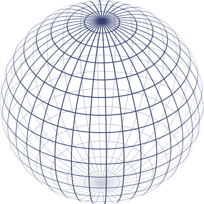
Example 1: Paraboloid
Consider the function . The shape of its graph is what's known as a "paraboloid", the three-dimensional equivalent of a parabola.

Here's what its contour map looks like:
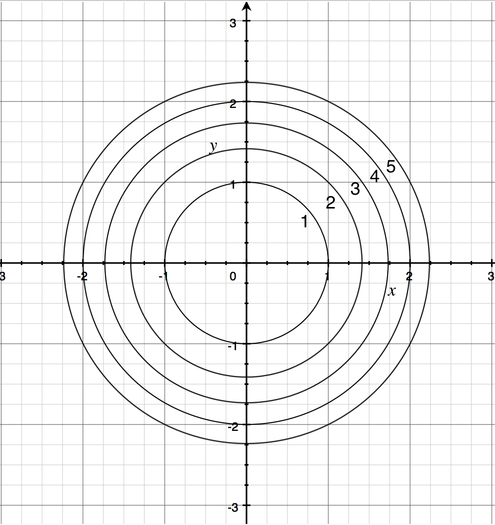
Notice that the circles are not evenly spaced. This is because the height of the graph increases more quickly as you get farther away from the origin. Therefore, increasing the height by a given amount requires a smaller step away from the origin in the input space.
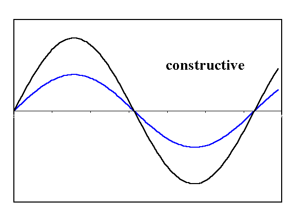
Example 2: Waves
How about the function ? Its graph looks super wavy:

And here is its contour map:

One feature worth pointing out here is that peaks and valleys can easily look very similar on a contour map, and can only be distinguished by reading the labels.
Example 3: Linear function
Next, let's look at . Its graph is a slanted plane.

This corresponds to a contour map with evenly spaced straight lines:

Example 4: Literal map
Contour maps are often used in actual maps to portray altitude in hilly terrains. The image on the right, for example, is a depiction of a certain crater on the moon.

Imagine walking around this crater. Where the contour lines are close together, the slope is rather steep. For instance, you descend from meters to meters over a very short distance. At the bottom, where lines are sparse, things are more flat, varying between meters and meters over larger distances.
Iso-suffs
The lines on a contour map have various names:
- Contour lines.
- Level sets, so named because they represent values of where the height of the graph remains unchanged, hence level.
- Isolines, where "iso" is a greek prefix meaning "same".
Depending on what the contour map represents, this iso prefix might come attached to a number of things. Here are two common examples from weather maps.
- An isotherm is a line on a contour map for a function representing temperature.
- An isobar is a line on a contour map representing pressure.
Gaining intuition from a contour map
You can tell how steep a portion of your graph is by how close the contour lines are to one another. When they are far apart, it takes a lot of lateral distance to increase altitude, but when they are close, altitude increases quickly for small lateral increments.
The level sets associated with heights that approach a peak of the graph will look like smaller and smaller closed loops, each one encompassing the next. Likewise for an inverted peak of the graph. This means you can spot the maximum or minimum of a function using its contour map by looking for sets of closed loops enveloping one another, like distorted concentric circles.


____________________________________________________


New technologies can make previously invisible phenomena visible. Nowhere is this more obvious than in the field of light microscopy and macro scope . camera technologies and associated image processing that have been a major driver of technical innovations in light microscopy. We describe five types of developments in camera technology: video-based analog contrast enhancement, charge-coupled devices (CCDs), intensified sensors, electron multiplying gain, and scientific complementary metal-oxide-semiconductor cameras, which, together, have had major impacts in light microscopy.
Technology for television broadcasts became available during the 1930s. The early developers of this technology were well aware of the potential usefulness of microscopy , the development of the television, in his landmark paper wrote, “Wide possibilities appear in application of such tubes in many fields as a substitute for the human eye, or for the observation of phenomena at present completely hidden from the eye, as in the case of the ultraviolet microscope” and Macro scope Joint . Over the following decades, while television technology became more mature and more widely accessible, its use in microscopes often appeared to be limited to classroom demonstrations. Shinya Inoué, a Japanese scientist whose decisive contributions to the field of cytoskeleton dynamics included ground-breaking new microscope technologies, described “the exciting displays of a giant amoeba, twice my height, crawling up on the auditorium screen at Princeton as I participated in a demonstration of the RCA projection video system to which we had coupled a phase-contrast microscope” . a video camera to a microscope setup for differential interference contrast (DIC), and discovered that sub-resolution structures could be made visible that were not visible when using the eye-pieces or on film . To view samples by eye, it was necessary to reduce the light intensity and to close down the iris diaphragm to increase apparent contrast, at the expense of reduced resolution. The video equipment enabled the use of a fully opened iris diaphragm and all available light, because one could now change the brightness and contrast and display the full resolution of the optical system on the television screen . Independently, yet at a similar time, Shinya Inoué used video cameras with auto-gain and auto-black level controls, which helped to improve the quality of both polarization and DIC microscope images . The Allens subsequently explored the use of frame memory to store a background image and continuously subtract it from a live video stream, further refining image quality . In practice, this background image was collected by slightly defocusing the microscope, accumulating many images, and averaging them . These new technologies enabled visualization of transport of vesicles in the squid giant axon , followed by visualization of such transport in extracts of the squid giant axon , leading to the development of microscopy-based assays for motor activity and subsequent purification of the motor protein, kinesin .
Until the development of the charge-coupled device (see next section), video cameras consisted of vacuum cathode ray tubes with a photosensitive front plate (target). These devices operated by scanning the cathode ray over the target while the resulting current varied with the amount of light “seen” by the scanned position. The analog signal (which most often followed the National Television System Committee (NTSC) standard of 30 frames per second and 525 lines) was displayed on a video screen. To store the data, either a picture of the screen was taken with a photo camera and silver emulsion-based film, or the video signal was stored on tape. Over the years, the design of both video cameras and recording equipment improved dramatically; cost reduction was driven by development for the consumer market. (In fact, to this day microscope camera technology development benefits enormously from industrial development aimed at the consumer electronics market.) However, the physical design of a vacuum tube and video tape recording device places limits on the minimum size possible, an important consideration motivating development of alternative technologies. Initially, digital processing units for background subtraction and averaging at video rate were home-built; but, later, commercial versions became available. The last widely used analog, a vacuum tube-based system used in microscopes, was probably the Hamamatsu Newvicon camera in combination with the Hamamatsu Argus image processor .
CCD Technology
Development of charge-coupled devices (CCDs) was driven by the desire to reduce the physical size of video cameras used in television stations to encourage their use by the consumer market. The CCD was invented in 1969 by Willard Boyle and George E. Smith at AT&T’s Bell Labs, an invention for which they received a half-share of the Nobel Prize in Physics in 2009. The essence of the invention was its ability to transfer charge from one area storage capacitor on the surface of a semiconductor to the next. In a CCD camera, these capacitors are exposed to light and they collect photo electrons through the photoelectric effect––in which a photon is converted into an electron. By shifting these charges along the surface of the detector to a readout node, the content of each storage capacitor can be determined and translated into a voltage that is equivalent to the amount of light originally hitting that area.
Various companies were instrumental in the development of the CCD, including Sony (for a short history of CCD camera development within Sony,
and Fairchild (Kodak developed the first digital camera based on a Fairchild 100 × 100-pixel sensor in 1975). These efforts quickly led to the wide availability of consumer-grade CCD cameras.
Even after CCD sensors had become technically superior to the older, tube-based sensors, it took time for everyone to transition from the tube-based camera technology and associated hardware, such as matching video recorders and image analyzers. One of the first descriptions of the use of a CCD sensor on a microscope can be found in Roos and Brady (1982), who attached a 1728-pixel CCD (which appears to be a linear CCD) to a standard microscope setup for Nomarski-type DIC microscopy. The authors built their own circuitry to convert the analog signals from the CCD to digital signals, which were stored in a micro-computer with 192 KB of memory. They were able to measure the length of sarcomeres in isolated heart cells at a time resolution of ~6 ms and a spatial precision of ~50 nm. Shinya Inoué’s book, Video Microscopy (1986), mentions CCDs as an alternative to tube-based sensors, but clearly there were very few CCDs in use on microscopes at that time. Remarkably, one of the first attempts to use deconvolution, an image-processing technique to remove out-of-focus “blur,” used photographic images that were digitized by a densitometer rather than a camera (Agard and Sedat, 1980). It was only in 1987 that the same group published a paper on the use of a CCD camera (Hiraoka et al., 1987). In that publication, the work of John A. Connor at AT&T’s Bell Labs is mentioned as the first use of the CCD in microscope imaging. Connor (1986) used a 320 × 512-pixel CCD camera from Photo-metrics (Tucson, AZ) for calcium imaging, using the fluorescent dye, Fura-2, as a reporter in rat embryonic nerve cells. Hiraoka et al. (1987) highlighted the advantages of the CCD technology, which included extraordinary sensitivity and numerical accuracy, and noted its main downside, slow speed. At the time, the readout speed was 50,000 pixels/s, and readout of the 1024 × 600-pixel camera took 13 s (speeds of 20 MHz are now commonplace, and would result in a 31-ms readout time for this particular camera).
One of the advantages of CCD cameras was their ability to expose the array for a defined amount of time. Rather than frame-averaging multiple short-exposure images in a digital video buffer (as was needed with a tube-based sensor), one could simply accumulate charge on the chip itself. This allowed for the recording of very sensitive measurements of dim, non-moving samples. As a result, CCD cameras became the detector of choice for (fixed) fluorescent samples during the 1990s.
Because CCDs are built using silicon, they inherit its excellent photon absorption properties at visible wavelengths. A very important parameter of camera performance is the fraction of light (photons) hitting the sensor that is converted into signal (in this case, photoelectrons). Hence, the quantum efficiency (QE) is expressed as the percentage of photoelectrons resulting from a given number of photons hitting the sensor. Even though the QE of crystalline silicon itself can approach 100%, the overlying electrodes and other structures reduce light absorption and, therefore, QE, especially at lower wavelengths (i.e., towards the blue range of the spectrum). One trick to increase the QE is to turn the sensor around so that its back faces the light source and to etch the silicon to a thin layer (10 –15 μm). Such back-thinned CCD sensors can have a QE of ~95% at certain wavelengths. The QE of charge-coupled devices tends to peak at wavelengths of around 550 nm, and drop off towards the red, because photons at wavelengths of 1100 nm are not energetic enough to elicit an electron in the silicon. Other tricks have been employed to improve the QE and its spectral properties, such as coating with fluorescent plastics to enhance the QE at lower wavelengths, changing the electrode material, or using micro-lenses that focus light on the most sensitive parts of the sensor. The Sony ICX285 sensor, which is still in use today, uses micro-lenses, achieving a QE of about 65% from ~450 –550 nm.
Concomitant with the advent of the CCD camera in microscope imaging was the widespread availability of desktop computers. Computers not only provided a means for digital storage of images, but also enabled image processing and analysis. Even though these desktop computers at first were unable to keep up with the data generated by a video rate camera (for many years, it was normal to store video on tape and digitize only sections of relevance), they were ideal for storage of images from the relatively slow CCD cameras. For data to enter the computer, analog-to-digital conversion (AD) is needed. AD conversion used to be a complicated step that took place in dedicated hardware or, later, in a frame grabber board or device, but nowadays it is often carried out in the camera itself (which provides digitized output). The influence of computers on microscopy cannot be overstated. Not only are computers now the main recording device, they also enable image reconstruction approaches––such as deconvolution, structured illumination, and super-resolution microscopy––that use the raw images to create realistic models for the microscopic object with resolutions that can be far greater than the original data. These models (or the raw data) can be viewed in many different ways, such as through 3D reconstructions, which are impossible to generate without computers. Importantly, computers also greatly facilitate extraction of quantitative information from the microscope data.

Intensified Sensors
The development of image intensifiers, which amplify the brightness of the image before it reaches the sensor or eye, started early in the twentieth century. These devices consisted of a photo cathode that converted photons into electrons, followed by an electron amplification mechanism, and, finally, a layer that converted electrons back into an image. The earliest image intensifiers were developed in the 1930s by Gilles Holst, who was working for Philips in the Netherlands (Morton, 1964). His intensifier consisted of a photo cathode upon which an image was projected in close proximity to a fluorescent screen. A voltage differential of several thousand volts accelerated electrons emitted from the photo cathode, directing them onto a phosphor screen. The high-energy electrons each produced many photons in the phosphor screen, thereby amplifying the signal. By cascading intensifiers, the signal can be intensified significantly. This concept was behind the so-called Gen I image-intensifiers.
The material of the photocathode determines the wavelength detected by the intensifier. Military applications required high sensitivity at infrared wavelengths, driving much of the early intensifier development; however, intensifiers can be built for other wavelengths, including X-rays.
Most intensifier designs over the last forty years or so (i.e., Gen II and beyond) include a micro-channel plate consisting of a bundle of thousands of small glass fibers bordered at the entrance and exit by nickel chrome electrodes. A high-voltage differential between the electrodes accelerates electrons into the glass fibers, and collisions with the wall elicit many more electrons, multiplying electrons coming from the photocathode. Finally, the amplified electrons from the micro-channel plate are projected onto a phosphor screen.
The sensitivity of an intensifier is ultimately determined by the quantum efficiency (QE) of the photocathode, and––despite decades of developments––it still lags significantly behind the QE of silicon-based sensors (i.e., the QE of the photocathode of a modern intensified camera peaks at around 50% in the visible region).
Intensifiers must be coupled to a camera in order to record images. For instance, intensifiers were placed in front of vidicon tubes either by fiber-optic coupling or by using lens systems in intensified vidicon cameras. Alternatively, intensifiers were built into the vacuum imaging tube itself. Probably the most well-known implementation of such a design is the silicon-intensifier target (SIT) camera. In this design, electrons from the photocathode are accelerated onto a silicon target made up of p-n junction silicon diodes. Each high-energy electron generates a large number of electron-hole pairs, which are subsequently detected by a scanning electron beam that generates the signal current. The SIT camera had a sensitivity that was several hundredfold higher than that of standard vidicon tubes (Inoué, 1986). SIT cameras were a common instrument in the 1980s and 1990s for low-light imaging. For instance, our lab used a SIT camera for imaging of sliding microtubules, using dark-field microscopy (e.g., Vale and Toyoshima, 1988) and other low-light applications such as fluorescence imaging. The John W. Sedat group used SIT cameras, at least for some time during the transition from film to CCD cameras, in their work on determining the spatial organization of DNA in the Drosophila nucleus (Gruenbaum et al., 1984).
When charge-coupled devices began to replace vidicon tubes as the sensor of choice, intensifiers were coupled to CCD or complementary metal-oxide-semiconductor (CMOS) sensors, either with a lens or by using fiber-optic bonding between the phosphor plate and the solid-state sensor. Such “ICCD” cameras can be quite compact and produce images from very low-light scenes at astonishing rates (for current commercial offerings, see, e.g., Stanford Photonics, 2016 and Andor, 2016a).
Intensified cameras played an important role at the beginning of single-molecule-imaging experimentation. Toshio Yanagida’s group performed the first published imaging of single fluorescent molecules in solution at room temperature. They visualized individual, fluorescently labeled myosin molecules as well as the turnover of individual ATP molecules, using total internal reflection microscopy, an ISIT camera (consisting of an intensifier in front of a SIT), and an ICCD camera (Funatsu et al., 1995). Until the advent of the electron multiplying charge-coupled device (EMCCD; see next section), ICCD cameras were the detector of choice for imaging of single fluorescent molecules. For instance, ICCD cameras were used to visualize single kinesin motors moving on axonemes (Vale et al., 1996), the blinking of green fluorescent protein (GFP) molecules (Dickson et al., 1997), and in demonstrating that F1-ATPase is a rotational motor that takes 120-degree steps (Yasuda et al., 1998).
Since the gain of an ICCD depends on the voltage differential between entrance and exit of the micro-channel plate, it can be modulated at extremely high rates (i.e., MHz rates). This gating not only provides an “electronic shutter,” but also can be used in more interesting ways. For example, the lifetime of a fluorescent dye (i.e., the time between absorption of a photon and emission of fluorescence) can be determined by modulating both the excitation light source and the detector gain. It can be appreciated that the emitted fluorescence will be delayed with respect to the excitation light, and that the amount of delay depends on the lifetime of the dye. By gating the detector at various phase delays with respect to the excitation light, signals with varying intensity will be obtained, from which the fluorescent lifetime can be deduced. This frequency-domain fluorescence lifetime imaging (FLIM) can be executed in wide-field mode, using an ICCD as a detector. FLIM is often used for measurement of Foerster energy transfer (FRET) between two dyes, which can be used as a proxy for the distance between the dyes. By using carefully designed probes, researchers have visualized cellular processes such as epidermal growth factor phosphorylation (Wouters and Bastiaens, 1999) and Rho GTPase activity (Hinde et al., 2013).
Electron Multiplying CCD Cameras
Despite the unprecedented sensitivity of intensified CCD cameras, which enable observation of single photons with relative ease, this technology has a number of drawbacks. These include the small linear range of the sensor (often no greater than a factor of 10), relatively low quantum efficiency (even the latest-generation ICCD cameras have a maximal QE of 50%), spreading of the signal due to the coupling of the intensifier to a CCD in an ICCD, and the possibility of irreversible sensor damage by high-light intensities, which can happen easily and at great financial cost. The signal spread was so significant that researchers were using non-amplified, traditional CCD cameras rather than ICCDs to obtain maximal localization precision in single-molecule experiments (see, e.g., Yildiz et al., 2003), despite the much longer readout times needed to collect sufficient signal above the readout (read) noise. Clearly, there was a need for CCD cameras with greater spatial precision, lower effective read noise, higher readout speeds, and a much higher damage threshold.
In 2001, both the British company, e2v technologies (Chelmsford, UK), and Texas Instruments (Dallas, TX) launched a new chip design that amplified the signal on the chip before reaching the readout amplifier, rather than using an external image intensifier. This on-chip amplification is carried out by an extra row of silicon “pixels,” through which all charge is transferred before reaching the readout amplifier. The well-to-well transfer in this special register is driven by a relatively high voltage, resulting in occasional amplification of electrons through a process called “impact ionization.” This process provides the transferred electrons with enough kinetic energy to knock an electron out of the silicon from the next well. Repeating this amplification in many wells (the highly successful e2v chip CCD97 has 536 elements in the amplification register) leads to very high effective amplification gains. Although the relation between voltage and gain is non-linear, the gain versus voltage curve has been calibrated by the manufacturer in modern electron multiplying (EM) CCD cameras, so that the end user can set a desired gain rather than a voltage. EM gain enables readout of the CCD at a much higher speed and read noise than normal, because the signal is amplified before readout. For instance, when the CCD readout noise is 30 e− (i.e., 30 electrons of noise per pixel) and a 100-fold EM gain is used, the effective read noise is 0.3 e−, using the unrealistic assumption that the EM gain itself does not introduce noise (read noise below 1 e− is negligible).
Amplification is never noise-free and several additional noise factors need to be considered when using EM gain. (For a thorough discussion of noise sources, see Andor, 2016b). Dark noise, or the occasional spontaneous accumulation of an electron in a CCD well, now becomes significant, since every “dark noise electron” will also be increased by EM amplification. Some impact ionization events take place during the normal charge transfers on the CCD. These “spurious charge” events are of no concern in a standard CCD, since they disappear in the noise floor dominated by readout noise, but they do become an issue when using EM gain. EM amplification itself is a stochastic process, and has noise characteristics very similar to that of the Poisson distributed photon shot noise, resulting in a noise factor (representing the additional noise over the noise expected from noise-free amplification) equal to √2, or ~1.41. Therefore, it was proposed that one can think of EM amplification as being noise-free but reducing the input signal by a factor of two, or halving the QE (Pawley, 2006).
Very quickly after their initial release around 2001, EMCCDs became the camera of choice for fluorescent, single-molecule detection. The most popular detector was the back-thinned EMCCD from e2v technologies, which has a QE reaching 95% in some parts of the spectrum and 512 × 512 × 16 μm-square pixels; through a frame transfer architecture, it can run continuously at ~30 frames per second (fps) full frame. One of the first applications of this technology in biological imaging was by the Jim Spudich group at Stanford University, who used the speed and sensitive detection offered by EMCCD cameras to image the mechanism of movement of the molecular motor protein, myosin VI. They showed that both actin-binding sites (heads) of this dimeric motor protein take 72-nm steps and that the heads move in succession, strongly suggesting a hand-over-hand displacement mechanism (Ökten et al., 2004).
One of the most spectacular contributions made possible by EMCCD cameras was the development of super-resolution localization microscopy. For many years, single-molecule imaging experiments had shown that it was possible to localize a single fluorescent emitter with high resolution, in principle limited only by the amount of photons detected. However, to image biological structures with high fidelity, one needs to image many single molecules, whose projections on the camera (the point spread function) overlap. As William E. Moerner and Eric Betzig explained in the 1990s, as long as one can separate the emission of single molecules based on any physical criteria, such as time or wavelength, it is possible to uniquely localize many single molecules within a diffraction-limited volume. Several groups implemented this idea in 2006, using blinking of fluorophores, either photo-activatable GFPs, in the case of photo-activated localization microscopy (PALM; Betzig et al., 2006) and fluorescence PALM (fPALM; Hess et al., 2006), or small fluorescent molecules, as in stochastic optical reconstruction microscopy (STORM; Rust et al., 2006). Clearly, the development and availability of fluorophores with the desired properties was essential for these advances (which is why the Nobel prize in Chemistry was awarded in 2014 to Moerner and Betzig, as well as Stefan W. Hell, who used non-camera based approaches to achieve super-resolution microscopy images). But successful implementation of super-resolution localization microscopy was greatly aided by EMCCD camera technology, which allowed the detection of single molecules with high sensitivity and low background, and at high speeds (the Betzig, Xiaowei Zhuang, and Samuel T. Hess groups all used EMCCD cameras in their work).
Other microscope-imaging modalities that operate at very low light levels have also greatly benefited from the use of EMCCD cameras. Most notably, spinning disk confocal microscopy is aided enormously by EMCCD cameras, since that microscopy enables visualization of the biological process of interest at lower light exposure of the sample and at higher speed than possible with a normal CCD. EMCCD-based imaging reduces photobleaching and photodamage of the live sample compared to CCDs, and offers better spatial resolution and larger linear dynamic range than do intensified CCD cameras. Hence, EMCCDs have largely replaced other cameras as the sensor of choice for spinning disk confocal microscopes .
Scientific CMOS Cameras
Charge-coupled device (CCD) technology is based on shifting charge between potential wells with high accuracy and the use of a single, or very few, readout amplifiers. (Note: It is possible to attach a unique readout amplifier to a subsection of the CCD, resulting in so-called multi-tap CCD sensors. But application of this approach has been limited in research microscopy). In active-pixel sensor (APS) architecture, each pixel contains not only a photodetector, but also an amplifier composed of transistors located adjacent to the photosensitive area of the pixel. These APS sensors are built using complementary metal-oxide-semiconductor (CMOS) technology, and are referred to as CMOS sensors. Because of their low cost, CMOS sensors were used for a long time in consumer-grade devices such as web cameras, cell phones, and digital cameras. However, they were considered far too noisy for use in scientific imaging, since every pixel contains its own amplifier, each slightly different from the other. Moreover, the transistors take up space on the chip that is not photosensitive, a problem that can be partially overcome by the use of micro-lenses to focus the light onto the photosensitive area of the sensor. Two developments, however, made CMOS cameras viable for microscopy imaging. First, Fairchild Imaging (Fairchild Imaging, 2016) improved the design of the CMOS sensor so that low read noise (around 1 electron per pixel) and high quantum efficiency (current sensors can reach 82% QE) became possible. These new sensors were named sCMOS (scientific CMOS). Second, the availability of field-programmable gate arrays (FPGAs), which are integrated circuits that can be configured after they have been produced (i.e., they can be used as custom-designed chips, cost much less because only the software has to be written. No new hardware needs to be designed). All current sCMOS cameras contain FPGAs that execute blemish corrections, such as reducing hot pixels and noisy pixels, and linearize the output of pixels, in addition to performing other functions, such as binning (pooling) of pixels. More and more image-processing functions are being integrated into these FPGAs. For instance, the latest sCMOS camera
Remarkably, sCMOS cameras can run at very high speeds (100 frames per s for a ~5-megapixel sensor), have desirable pixel sizes (the standard is 6.5 μm2, which matches the resolution provided by the often used 100 × 1.4-na objective lens; see Maddox et al., 2003 for an explanation), and cost significantly less than electron multiplying CCD (EMCCD) cameras. These features led to the rapid adoption of these cameras, even though the early models still had obvious defects, such as uneven dark image, non-linear pixel response (most pronounced around pixel value 2048 due to the use of separate digital-to-analog converters for the low- and high-intensity ranges), and the rolling shutter mode, which causes the exposure to start and end at varying time points across the chip (up to 10 ms apart). The speed, combined with large pixel number and low-read noise, makes sCMOS cameras highly versatile for most types of microscopy. In practice, however, EMCCDs still offer an advantage under extremely low-light conditions, such as is often encountered in spinning disk confocal microscopy (Fig. 3; Oreopoulos et al., 2013). However, super-resolution microscopy can make good use of the larger field of view and higher speed of sCMOS cameras, resulting in much faster data acquisition of larger areas. For example, acquisition of reconstructed super-resolution images at a rate of 32 per s using sCMOS cameras has been demonstrated (Huang et al., 2013). Another application that has greatly benefited from sCMOS cameras is light sheet fluorescence microscopy, in which objects ranging in size from single cells to small animals are illuminated sideways, such that only the area to be imaged is illuminated, greatly reducing phototoxicity. The large field of view, low-read noise, and high speed of sCMOS cameras has, for instance, made it possible to image calcium signaling in 80% of the neurons of a zebrafish embryo at 0.8 Hz (Ahrens et al., 2013). A recent development is lattice light sheet microscopy, which uses a very thin sheet and allows for imaging of individual cells at high resolution for extended periods of time. Lattice light sheet microscopes use sCMOS cameras because of their high speed, low-read noise, and large field of view (Chen et al., 2015). New forms and improvements in light sheet microscopy will occur in the next several years, and make significant contributions to the understanding of biological systems.

Comparison of the electron multiplying charge-coupled device (EMCCD) and scientific complementary metal-oxide-semiconductor (sCMOS) cameras for use with a spinning disk confocal microscope. Adjacent cells were imaged, making use of either an EMCCD or sCMOS camera, using different tube lenses such that the pixel size in the image plane was the same for both (16-μm pixels for the EMCCD, with a 125-mm tube lens; 6.5-μm pixels for the sCMOS, with a 50-mm tube lens). (Reprinted from fig. 9.8, panel b, of Oreopoulos, J., et al., 2013, Methods Cell Biol. 123: 153–175, with permission from Elsevier.) from Photometrics can execute a complicated noise reduction algorithm on the FPGA of the camera before the image reaches the computer
Summary and Outlook

Microscope imaging has progressed from the written recording of qualitative observations to a quantitative technique with permanent records of images. This leap was made possible through the emergence of highly quantitative, sensitive, and fast cameras, as well as computers, which make it possible to capture, display, and analyze the data generated by the cameras. It is safe to say that, despite notable improvements in microscope optics, progress in microscopy over the last three decades has been largely driven by sensors and analysis of digital images; structured illumination, super-resolution, lifetime, and light sheet microscopy, to name a few, would have been impossible without fast quantitative sensors and computers. The development of camera technologies was propelled by the interests of the military, the consumer market, and researchers, who have benefited from the much larger economic influence of the other groups.
Camera technology has become very impressive, pushing closer and closer to the theoretical limits. The newest sCMOS cameras have an effective read noise of about 1 e− and high linearity over a range spanning almost 4 orders of magnitude; they can acquire 5 million pixels at a rate of 100 fps and have a maximal QE of 82%. Although there is still room for improvement, these cameras enable sensitive imaging at the single-molecule level, probe biochemistry in living cells, and image organs or whole organisms at a fast rate and high resolution in three dimensions. The biggest challenge is to make sense of the enormous amount of data generated. At maximum rate, sCMOS cameras produce data at close to 1 GB/s, or 3.6 TB/h, making it a challenge to even store on computer disk, let alone analyze the images with reasonable throughput. Reducing raw data to information useful for researchers, both by extracting quantitative measurements from raw data and by visualization (especially in 3D), is increasingly becoming a bottleneck and an area where improvements and innovations could have profound effects on obtaining new biological insights. We expect that this data reduction will occur more and more “upstream,” close to the sensor itself, and that data analysis and data reduction will become more integrated with data acquisition. The aforementioned noise filters built into the new Photometrics sCMOS camera, as well as recently released software by Andor that can transfer data directly from the camera to the computer’s graphical processing unit (GPU) for fast analysis, foreshadow such developments. Whereas researchers now still consider the entire acquired image as the de facto data that needs to be archived, we may well transition to a workflow in which images are quickly reduced to the measurements of interest (using well-described, open, and reproducible procedures), either by computer processing in the camera itself or in closely connected computational units. Developments in this area will open new possibilities for the ways in which scientists visualize and analyze biological samples.
Abbreviations
| AD | analog-to-digital conversion |
| APS | active pixel sensor |
| CCD | charge-coupled device |
| CMOS | complementary metal-oxide-semiconductor |
| DIC | differential interference contrast |
| EMCCD | electron multiplying charge-coupled device |
| FLIM | fluorescence lifetime imaging microscopy |
| fps | frames per second |
| FRET | Foerster resonance energy transfer |
| GFPs | green fluorescent proteins |
| PALM | photoactivated localization microscopy |
| QE | quantum efficiency |
| sCMOS | scientific complementary metal-oxide-semiconductor |
| SIT | silicon-intensifier target |
| STORM | stochastic optical reconstruction microscopy |
A.XO Light Sensors
__________________________________________________________________________________
Light Sensors are photoelectric devices that convert light energy (photons) whether visible or infra-red light into an electrical (electrons) signal
A Light Sensor generates an output signal indicating the intensity of light by measuring the radiant energy that exists in a very narrow range of frequencies basically called “light”, and which ranges in frequency from “Infra-red” to “Visible” up to “Ultraviolet” light spectrum.
The light sensor is a passive devices that convert this “light energy” whether visible or in the infra-red parts of the spectrum into an electrical signal output. Light sensors are more commonly known as “Photoelectric Devices” or “Photo Sensors” because the convert light energy (photons) into electricity (electrons).
Photoelectric devices can be grouped into two main categories, those which generate electricity when illuminated, such as Photo-voltaics or Photo-emissives etc, and those which change their electrical properties in some way such as Photo-resistors or Photo-conductors. This leads to the following classification of devices.
- • Photo-emissive Cells – These are photodevices which release free electrons from a light sensitive material such as caesium when struck by a photon of sufficient energy. The amount of energy the photons have depends on the frequency of the light and the higher the frequency, the more energy the photons have converting light energy into electrical energy.
- • Photo-conductive Cells – These photodevices vary their electrical resistance when subjected to light. Photoconductivity results from light hitting a semiconductor material which controls the current flow through it. Thus, more light increase the current for a given applied voltage. The most common photoconductive material is Cadmium Sulphide used in LDR photocells.
- • Photo-voltaic Cells – These photodevices generate an emf in proportion to the radiant light energy received and is similar in effect to photoconductivity. Light energy falls on to two semiconductor materials sandwiched together creating a voltage of approximately 0.5V. The most common photovoltaic material is Selenium used in solar cells.
- • Photo-junction Devices – These photodevices are mainly true semiconductor devices such as the photodiode or phototransistor which use light to control the flow of electrons and holes across their PN-junction. Photojunction devices are specifically designed for detector application and light penetration with their spectral response tuned to the wavelength of incident light.
The Photoconductive Cell
A Photoconductive light sensor does not produce electricity but simply changes its physical properties when subjected to light energy. The most common type of photoconductive device is the Photoresistor which changes its electrical resistance in response to changes in the light intensity.
Photoresistors are Semiconductor devices that use light energy to control the flow of electrons, and hence the current flowing through them. The commonly used Photoconductive Cell is called the Light Dependent Resistor or LDR.
The Light Dependent Resistor

Typical LDR
As its name implies, the Light Dependent Resistor (LDR) is made from a piece of exposed semiconductor material such as cadmium sulphide that changes its electrical resistance from several thousand Ohms in the dark to only a few hundred Ohms when light falls upon it by creating hole-electron pairs in the material.
The net effect is an improvement in its conductivity with a decrease in resistance for an increase in illumination. Also, photoresistive cells have a long response time requiring many seconds to respond to a change in the light intensity.
Materials used as the semiconductor substrate include, lead sulphide (PbS), lead selenide (PbSe), indium antimonide (InSb) which detect light in the infra-red range with the most commonly used of all photoresistive light sensors being Cadmium Sulphide (Cds).
Cadmium sulphide is used in the manufacture of photoconductive cells because its spectral response curve closely matches that of the human eye and can even be controlled using a simple torch as a light source. Typically then, it has a peak sensitivity wavelength (λp) of about 560nm to 600nm in the visible spectral range.
The Light Dependent Resistor Cell

The most commonly used photoresistive light sensor is the ORP12 Cadmium Sulphide photoconductive cell. This light dependent resistor has a spectral response of about 610nm in the yellow to orange region of light. The resistance of the cell when unilluminated (dark resistance) is very high at about 10MΩ’s which falls to about 100Ω’s when fully illuminated (lit resistance).
To increase the dark resistance and therefore reduce the dark current, the resistive path forms a zigzag pattern across the ceramic substrate. The CdS photocell is a very low cost device often used in auto dimming, darkness or twilight detection for turning the street lights “ON” and “OFF”, and for photographic exposure meter type applications.

Connecting a light dependant resistor in series with a standard resistor like this across a single DC supply voltage has one major advantage, a different voltage will appear at their junction for different levels of light.
The amount of voltage drop across series resistor, R2is determined by the resistive value of the light dependant resistor, RLDR. This ability to generate different voltages produces a very handy circuit called a “Potential Divider” or Voltage Divider Network.
As we know, the current through a series circuit is common and as the LDR changes its resistive value due to the light intensity, the voltage present at VOUT will be determined by the voltage divider formula. An LDR’s resistance, RLDR can vary from about 100Ω in the sun light, to over 10MΩ in absolute darkness with this variation of resistance being converted into a voltage variation at VOUT as shown.
One simple use of a Light Dependent Resistor, is as a light sensitive switch as shown below.

LDR Switch
This basic light sensor circuit is of a relay output light activated switch. A potential divider circuit is formed between the photoresistor, LDR and the resistor R1. When no light is present ie in darkness, the resistance of the LDR is very high in the Megaohms (MΩ) range so zero base bias is applied to the transistor TR1 and the relay is de-energised or “OFF”.
As the light level increases the resistance of the LDR starts to decrease causing the base bias voltage at V1 to rise. At some point determined by the potential divider network formed with resistor R1, the base bias voltage is high enough to turn the transistor TR1 “ON” and thus activate the relay which in turn is used to control some external circuitry. As the light level falls back to darkness again the resistance of the LDR increases causing the base voltage of the transistor to decrease, turning the transistor and relay “OFF” at a fixed light level determined again by the potential divider network.
By replacing the fixed resistor R1 with a potentiometer VR1, the point at which the relay turns “ON” or “OFF” can be pre-set to a particular light level. This type of simple circuit shown above has a fairly low sensitivity and its switching point may not be consistent due to variations in either temperature or the supply voltage. A more sensitive precision light activated circuit can be easily made by incorporating the LDR into a “Wheatstone Bridge” arrangement and replacing the transistor with an Operational Amplifier as shown.
Light Level Sensing Circuit

In this basic dark sensing circuit, the light dependent resistor LDR1 and the potentiometer VR1 form one adjustable arm of a simple resistance bridge network, also known commonly as a Wheatstone bridge, while the two fixed resistors R1 and R2 form the other arm. Both sides of the bridge form potential divider networks across the supply voltage whose outputs V1 and V2 are connected to the non-inverting and inverting voltage inputs respectively of the operational amplifier.
The operational amplifier is configured as a Differential Amplifier also known as a voltage comparator with feedback whose output voltage condition is determined by the difference between the two input signals or voltages, V1 and V2. The resistor combination R1 and R2 form a fixed voltage reference at input V2, set by the ratio of the two resistors. The LDR – VR1 combination provides a variable voltage input V1 proportional to the light level being detected by the photoresistor.
As with the previous circuit the output from the operational amplifier is used to control a relay, which is protected by a free wheel diode, D1. When the light level sensed by the LDR and its output voltage falls below the reference voltage set at V2 the output from the op-amp changes state activating the relay and switching the connected load.
Likewise as the light level increases the output will switch back turning “OFF” the relay. The hysteresis of the two switching points is set by the feedback resistor Rf can be chosen to give any suitable voltage gain of the amplifier.
The operation of this type of light sensor circuit can also be reversed to switch the relay “ON” when the light level exceeds the reference voltage level and vice versa by reversing the positions of the light sensor LDR and the potentiometer VR1. The potentiometer can be used to “pre-set” the switching point of the differential amplifier to any particular light level making it ideal as a simple light sensor project circuit.
Photojunction Devices
Photojunction Devices are basically PN-Junction light sensors or detectors made from silicon semiconductor PN-junctions which are sensitive to light and which can detect both visible light and infra-red light levels. Photo-junction devices are specifically made for sensing light and this class of photoelectric light sensors include the Photodiode and the Phototransistor.
The Photodiode.

Photo-diode
The construction of the Photodiode light sensor is similar to that of a conventional PN-junction diode except that the diodes outer casing is either transparent or has a clear lens to focus the light onto the PN junction for increased sensitivity. The junction will respond to light particularly longer wavelengths such as red and infra-red rather than visible light.
This characteristic can be a problem for diodes with transparent or glass bead bodies such as the 1N4148 signal diode. LED’s can also be used as photodiodes as they can both emit and detect light from their junction. All PN-junctions are light sensitive and can be used in a photo-conductive unbiased voltage mode with the PN-junction of the photodiode always “Reverse Biased” so that only the diodes leakage or dark current can flow.
The current-voltage characteristic (I/V Curves) of a photodiode with no light on its junction (dark mode) is very similar to a normal signal or rectifying diode. When the photodiode is forward biased, there is an exponential increase in the current, the same as for a normal diode. When a reverse bias is applied, a small reverse saturation current appears which causes an increase of the depletion region, which is the sensitive part of the junction. Photodiodes can also be connected in a current mode using a fixed bias voltage across the junction. The current mode is very linear over a wide range.
Photo-diode Construction and Characteristics

When used as a light sensor, a photodiodes dark current (0 lux) is about 10uA for geranium and 1uA for silicon type diodes. When light falls upon the junction more hole/electron pairs are formed and the leakage current increases. This leakage current increases as the illumination of the junction increases.
Thus, the photodiodes current is directly proportional to light intensity falling onto the PN-junction. One main advantage of photodiodes when used as light sensors is their fast response to changes in the light levels, but one disadvantage of this type of photodevice is the relatively small current flow even when fully lit.
The following circuit shows a photo-current-to-voltage converter circuit using an operational amplifier as the amplifying device. The output voltage (Vout) is given as Vout = IP*Rƒ and which is proportional to the light intensity characteristics of the photodiode.
This type of circuit also utilizes the characteristics of an operational amplifier with two input terminals at about zero voltage to operate the photodiode without bias. This zero-bias op-amp configuration gives a high impedance loading to the photodiode resulting in less influence by dark current and a wider linear range of the photocurrent relative to the radiant light intensity. Capacitor Cf is used to prevent oscillation or gain peaking and to set the output bandwidth (1/2πRC).
Photo-diode Amplifier Circuit

Photodiodes are very versatile light sensors that can turn its current flow both “ON” and “OFF” in nanoseconds and are commonly used in cameras, light meters, CD and DVD-ROM drives, TV remote controls, scanners, fax machines and copiers etc, and when integrated into operational amplifier circuits as infrared spectrum detectors for fibre optic communications, burglar alarm motion detection circuits and numerous imaging, laser scanning and positioning systems etc.
The Phototransistor

Photo-transistor
An alternative photo-junction device to the photodiode is the Phototransistor which is basically a photodiode with amplification. The Phototransistor light sensor has its collector-base PN-junction reverse biased exposing it to the radiant light source.
Phototransistors operate the same as the photodiode except that they can provide current gain and are much more sensitive than the photodiode with currents are 50 to 100 times greater than that of the standard photodiode and any normal transistor can be easily converted into a phototransistor light sensor by connecting a photodiode between the collector and base.
Phototransistors consist mainly of a bipolar NPN Transistor with its large base region electrically unconnected, although some phototransistors allow a base connection to control the sensitivity, and which uses photons of light to generate a base current which in turn causes a collector to emitter current to flow. Most phototransistors are NPN types whose outer casing is either transparent or has a clear lens to focus the light onto the base junction for increased sensitivity.
Photo-transistor Construction and Characteristics

In the NPN transistor the collector is biased positively with respect to the emitter so that the base/collector junction is reverse biased. therefore, with no light on the junction normal leakage or dark current flows which is very small. When light falls on the base more electron/hole pairs are formed in this region and the current produced by this action is amplified by the transistor.
Usually the sensitivity of a phototransistor is a function of the DC current gain of the transistor. Therefore, the overall sensitivity is a function of collector current and can be controlled by connecting a resistance between the base and the emitter but for very high sensitivity optocoupler type applications, Darlington phototransistors are generally used.

Photo-darlington
Photodarlington transistors use a second bipolar NPN transistor to provide additional amplification or when higher sensitivity of a photodetector is required due to low light levels or selective sensitivity, but its response is slower than that of an ordinary NPN phototransistor.
Photo darlington devices consist of a normal phototransistor whose emitter output is coupled to the base of a larger bipolar NPN transistor. Because a darlington transistor configuration gives a current gain equal to a product of the current gains of two individual transistors, a photodarlington device produces a very sensitive detector.
Typical applications of Phototransistors light sensors are in opto-isolators, slotted opto switches, light beam sensors, fibre optics and TV type remote controls, etc. Infrared filters are sometimes required when detecting visible light.
Another type of photojunction semiconductor light sensor worth a mention is the Photo-thyristor. This is a light activated thyristor or Silicon Controlled Rectifier, SCR that can be used as a light activated switch in AC applications. However their sensitivity is usually very low compared to equivalent photodiodes or phototransistors.
To help increase their sensitivity to light, photo-thyristors are made thinner around the gate junction. The downside to this process is that it limits the amount of anode current that they can switch. Then for higher current AC applications they are used as pilot devices in opto-couplers to switch larger more conventional thyristors.
Photovoltaic Cells.
The most common type of photovoltaic light sensor is the Solar Cell. Solar cells convert light energy directly into DC electrical energy in the form of a voltage or current to a power a resistive load such as a light, battery or motor. Then photovoltaic cells are similar in many ways to a battery because they supply DC power.
However, unlike the other photo devices we have looked at above which use light intensity even from a torch to operate, photovoltaic solar cells work best using the suns radiant energy.
Solar cells are used in many different types of applications to offer an alternative power source from conventional batteries, such as in calculators, satellites and now in homes offering a form of renewable power.

Photovoltaic Cell
Photovoltaic cells are made from single crystal silicon PN junctions, the same as photodiodes with a very large light sensitive region but are used without the reverse bias. They have the same characteristics as a very large photodiode when in the dark.
When illuminated the light energy causes electrons to flow through the PN junction and an individual solar cell can generate an open circuit voltage of about 0.58v (580mV). Solar cells have a “Positive” and a “Negative” side just like a battery.
Individual solar cells can be connected together in series to form solar panels which increases the output voltage or connected together in parallel to increase the available current. Commercially available solar panels are rated in Watts, which is the product of the output voltage and current (Volts times Amps) when fully lit.
Characteristics of a typical Photovoltaic Solar Cell.

The amount of available current from a solar cell depends upon the light intensity, the size of the cell and its efficiency which is generally very low at around 15 to 20%. To increase the overall efficiency of the cell commercially available solar cells use polycrystalline silicon or amorphous silicon, which have no crystalline structure, and can generate currents of between 20 to 40mA per cm2.
Other materials used in the construction of photovoltaic cells include Gallium Arsenide, Copper Indium Diselenide and Cadmium Telluride. These different materials each have a different spectrum band response, and so can be “tuned” to produce an output voltage at different wavelengths of light.
B. XO CCD SENSOR IN CAMERAS
_____________________________________________________

In place of the film used in conventional film cameras, digital cameras incorporate an electronic component known as an image sensor. Most digital cameras are equipped with the image sensor known as a CCD Sensors, a semiconductor sensor that converts light into electrical signals. CCD Sensors are made up of tiny elements known as pixels. Expressions such as "2-megapixel" and "4-megapixel" refer to the number of pixels comprising the CCD Sensors of a camera. Each pixel is in fact a tiny photo diode that is sensitive to light and becomes electrically charged in accordance with the strength of light that strikes it. These electrical charges are relayed much like buckets of water in a bucket line, to eventually be converted into electrical signals.
The Way Light Is Converted Into Electric Current
The surface of a CCD Sensors is packed with photodiodes, each of which senses light and accumulates electrical charge in accordance with the strength of light that strikes it. Let's take a look at what happens in each photodiode. Photodiodes are, in fact, semiconductors, the most basic of which is a pn pair made up of a p-type and an n-type semiconductor. If a plus electrode (anode) is attached to the p-type side, and a minus electrode (cathode) is attached to the n-type side of the pn pair, and electric current is then passed through this circuit, current flows through the semiconductor. This is known as forward bias. If you create a reversed circuit by attaching a plus electrode to the n-type side, and a minus electrode to the p-type side of the pn pair, then electrical current will be unable to flow. This is known as reverse bias. Photodiodes possess this reverse bias structure. The main difference from standard semiconductors is the way in which they accumulate electrical charge in direct proportion to the amount of light that strikes them.

Photodiodes Accumulate Electrical Charge
Photodiodes are designed to enable light to strike them on their p-type sides. When light strikes this side, electrons and holes are created within the semiconductor in a photoelectric effect. Light of a short wavelength that strikes the photodiode is absorbed by the p-type layer, and the electrons created as a result are attracted to the n-type layer. Light of a long wavelength reaches the n-type layer, and the holes created as a result in the n-type layer are attracted to the p-type layer. In short, holes gather on the p-type side, which accumulates positive charge, while electrons gather on the n-type side, which accumulates negative charge. And because the circuit is reverse-biased, the electrical charges generated are unable to flow. The brighter the light that hits the photodiode, the greater the electrical charge that will accumulate within it. This accumulation of electrical charge at the junction of the pn pair when light strikes is known as a photovoltaic effect. Photodiodes are basically devices that make use of such photovoltaic effects to convert light into electrical charge, which accumulates in direct proportion to the strength of the light striking them. Photodiodes are also at work in our everyday lives in such devices as infrared remote control sensors and camera exposure meters.

CCD Sensors Relay Electrical Charge Like Buckets of Water in a Bucket Line
CCD Sensors comprise photodiodes and mechanisms consisting of polysilicon gates for transferring the charges accumulating within them to the edge of the CCD. The charges themselves cannot be read as electrical signals, and need to be transferred across the CCD Sensors to the edge, where they are converted into voltage. By applying series of pulses, the charges accumulated at each photodiode are relayed in succession, much like buckets of water in a bucket line, down the rows of photodiodes to the edge. CCD is the abbreviation of "Charge-Coupled Device," and "Charge-Coupled" means the way charges are moved through gates from one photodiode to the next.

C . XO The EARTH ___ SPACE AND LIGHT
---------------------------------------------------------------------------------

Space is filled with waves of various wavelengths. In addition to visible light, there are wavelengths that cannot be seen by the naked eye, such as radio waves and infrared, ultraviolet, X-, and gamma rays. These are collectively known as electromagnetic waves because they pass through space by alternately oscillating between electric and magnetic fields. Light is a type of electromagnetic wave. The electromagnetic waves reaching us consist of only a portion of the visible light, near-infrared rays and radio waves from space because the earth is surrounded by a layer of gases known as the atmosphere. This structure is intimately related to the existence of life on earth.
Does Light Nurture Life?
Life on earth receives the blessings of the light emitted by the sun. The energy that reaches the earth from the sun is about 2 calories per square centimeter per minute, the figure known as solar constant. Calculations based on this figure indicate that every second the sun emits as much energy into space as burning 10 quadrillion (10,000 trillion) tons of coal. The greatest of the sun's gifts to earth is photosynthesis by plants. When a material absorbs the energy of light, the light is changed into heat, thereby raising the object's temperature. There are also cases where fluorescence or phosphorescence is emitted, but most of the time materials do not change. Sometimes, however, materials do chemically react to light. This is called a "photochemical reaction." Photochemical reactions do not occur with infrared light, but happen primarily when visible light and ultraviolet rays, which have shorter wavelengths, are absorbed.
Photosynthesis also is a type of chemical reaction. Plants use the energy of sunlight to synthesize glucose from carbon dioxide and water. They then use this glucose to produce such materials as starch and cellulose. In short, photosynthesis stores the energy of sunlight in the form of glucose. All animals, including humans, live by eating these plants, thereby absorbing the oxygen produced during photosynthesis and indirectly taking in the energy of sunlight. In other words, sunlight is a source of life on earth. We do not yet know the detail of how plants conduct photosynthesis, but in green plants, chloroplasts within cells are known to play a crucial role.

Does the Earth Have Windows?
The earth is surrounded by layers of gases called the atmosphere. Some wavelengths of electromagnetic waves arriving from space are absorbed by the atmosphere and never reach the surface of our planet. Take a look at the following diagram. The earth's atmosphere absorbs the majority of ultraviolet, X-, and gamma rays, which are all shorter wavelengths than visible light. High energy X- and gamma rays would damage organisms and cells of creatures if they were to reach the earth's surface directly. Fortunately, the atmosphere protects life on earth. Long-wavelength radio waves and infrared rays also do not reach the surface. The electromagnetic waves we can generally observe on the ground consist of visible light, which is difficult for the atmosphere to absorb, near-infrared rays, and some electromagnetic waves. These wavelength ranges are called atmospheric windows. Ground-based astronomical observation employs optical and radio telescopes that take advantage of atmospheric windows. Infrared, X-, and gamma rays, for which atmospheric windows are closed, can only be observed using balloons and astronomical satellites outside the earth's atmosphere.

What Does Invisible Light Do?
Electromagnetic waves are all around us. This includes not only visible light, but also invisible ultraviolet and infrared rays. Infrared rays, with wavelengths longer than visible light, are also a familiar part of electrical appliances. Infrared rays with wavelengths of 2,500 nm and less are called near-infrared rays and are used in TV and VCR remote controllers, as well as in fiber-optic communications. Wavelengths above 2,500 nm are called far-infrared rays and are used in heaters and stoves.

Ultraviolet rays, with wavelengths shorter than visible light, pack high energy that results in sunburns and faded curtains. Ultraviolet rays with wavelengths of 315 nm and less are particularly dangerous because they destroy the DNA within the cells of living creatures. The bactericidal effect of ultraviolet rays is employed for medical implements, but we also know that large doses of these rays can trigger diseases such as skin cancer and have an impact on the entire ecosystem. Ultraviolet rays are suspected in ozone layer destruction, one of the global environmental issues that has been focused on in recent years. Near an altitude of 25 km, there is a rather thick ozone layer of 15 parts per million (ppm). This layer absorbs ultraviolet rays with wavelengths of 350 nm and less, thereby preventing them from reaching the earth's surface, where they would devastate life. Part of the ozone layer is being destroyed by chlorofluorocarbons (CFCs) that are used in refrigerators and air conditioners. "Ozone holes," where the level of ozone is extremely low, can be observed in the Antarctic and other places.

What If Light Does Nasty Things?
"Photochemical smog" is another environmental problem caused by photochemical reactions. Light causes automobile exhaust to chemically react and form irritating materials that produce smog. This occurs around high-traffic roadways on hot, windless days. Automobile engines and other machinery emit nitrogen monoxide (NO). Immediately after entering the atmosphere, NO reacts with oxygen molecules, transforming into nitrogen dioxide, a brownish gas that readily absorbs visible light, causing a photochemical reaction that breaks it down into NO and oxygen atoms. However, this NO once again immediately reacts with oxygen molecules, transforming back into nitrogen dioxide.


Through the process of photolysis, sunlight produces a vast amount of highly reactive oxygen atoms from a small amount of nitrogen dioxide. (A reaction is taking place through which single oxygen molecules consisting of two oxygen atoms are dissociated to form oxygen atoms.) The resulting oxygen atoms bond with oxygen molecules, forming ozone, and with other organic compounds in exhaust gas, forming peroxides. Ozone and peroxides are a source of eye and throat irritati

D. XO LIGHT AND COLOUR
______________________________________________________

The human eye resembles a camera. It has an iris and a lens, and the retina-a membrane deep inside the eye-functions much like film. Light passes through the lens of the eye and strikes the retina, thereby stimulating its photoreceptor cells, which in turn emit a signal. This signal travels over the optic nerve to the brain, where color is perceived. There are two types of photoreceptor cells known as "cones" and "rods." Rods detect brightness and darkness, while cones detect color. Between the two, there are some 200 million photoreceptor cells. Cones are further classified into L, M, and S cones, each of which senses a different color wavelength, allowing us to perceive color.
Why Can We See Color?
Sunlight itself is colorless and is therefore called white light. So, why can we see color in the objects around us? An object's color depends on its properties. For example, an object that looks red when light is shined on it will appear bright red when only red light is used. When only blue light is used, however, the same object will look dark. An object that normally looks red reflects red light most intensely while absorbing other colors of light. In short, we see an object's color based on what color it is reflecting most intensely.

Light is comprised of the three primary colors: red, green and blue. Combining these three primary colors of light yields white, while other combinations can produce all the colors we see. The human retina has L, M and S cones, which act as sensors for red, green and blue, respectively.

Why do things appear in 3-D? (1)
The world as seen by humans is a 3-dimensional space. Why are we able to perceive the depth of objects despite the human retina sensing flat 2-dimensional information?
Humans have two eyes, which are separated horizontally (by a distance of approximately 6.5 cm). Because of this, the left eye and right eye view objects from slightly different angles (this is called "binocular disparity") and the images sensed by the retinas differ slightly. This difference is processed in the brain (in the visual area of the cerebral cortex) and recognized as 3-dimensional information.
Movie and television images are flat, 2-dimensional in nature, but 3-D movies and 3-D television utilize this "binocular disparity" to create different images for the left and right eyes. These two types of images are delivered to the left and right eyes, which provides the sensation of a 3-D image.
3-D movies generally require 3-D glasses to enable viewers to see two types of images on a single screen. Projection methods vary from theater to theater, as do the types of glasses used. Some typical types of 3-D glasses include color filter (anaglyph) glasses, polarized glasses, and shutter glasses. In the color filter method, images are divided into separate RGB wavelengths. When passed through glasses with different colored filters on the left and right lenses, the image matching each eye enters. In the polarization method, two types of polarized light differing by 90 degrees are applied to images, and these are separated using a polarization filter in the glasses. The shutter method switches between the left and right images. Shutter glasses alternate the opening and closing of the left and right shutters in sync with the switching of images on the screen, delivering the respective images to each eye. Because switching takes place over extremely short periods of time, the images appear without breaks due to the "afterimage effect" that takes place in human eyes.

Why do things appear in 3-D? (2)
Like 3-D movies, 3-D televisions make use of "binocular disparity." The mechanism, however, is slightly different. 3-D televisions display two types of images by attaching optical components to the display panel or embedding fine slits in it. A typical optical component is the "lenticular lens," a lens sheet with a cross-section characterized by a semi-circular pattern, which is placed in front of the television screen, resulting in the image created by the pixels for each eye entering the left and right eyes of the viewer separately. This method enables viewers to enjoy 3-dimensional video without the need for special glasses, but the viewing location is limited. For example, when c represents the distance from the television screen to the lenticular lens, L the distance from the lenticular lens to the viewer, and f the focal length of the lenticular lens, the following relationship applies: 1/c + 1/L = 1/f. Once c and f have been determined, then the viewing position L becomes fixed. Furthermore, the frame sequential method, which alternates between two types of images without the use of optical components like the shutter method used in films, has recently been practically implemented for 3-D television and is becoming the most widely adopted technology. This method, however, requires glasses with shutters synchronized with the switching of images.
Other technologies that enable the world of 3-D to be enjoyed with even higher levels of realism are also being developed. A human's depth perception not only utilizes binocular disparity, but also "motion parallax," which enables not only the front of an object to be seen, but also the sides and back of the object when the object moves or is seen from a different angle. There are also systems that incorporate compact cameras and positional sensors like the HMD (head mounted display) used in Canon's MR (Mixed Reality) technology, which changes images in real time according to the movement of the viewer to provide a realistic 3-D video experience. Technology that makes use of holography is also under consideration.
Other technologies that enable the world of 3-D to be enjoyed with even higher levels of realism are also being developed. A human's depth perception not only utilizes binocular disparity, but also "motion parallax," which enables not only the front of an object to be seen, but also the sides and back of the object when the object moves or is seen from a different angle. There are also systems that incorporate compact cameras and positional sensors like the HMD (head mounted display) used in Canon's MR (Mixed Reality) technology, which changes images in real time according to the movement of the viewer to provide a realistic 3-D video experience. Technology that makes use of holography is also under consideration.


Does Light from Receding Objects Appear Reddish?
The "Doppler effect" acts on sound. For example, the pitch of an ambulance siren becomes higher as it moves toward you and lower as it moves away. This phenomenon occurs because many sound waves are squeezed into a shortening distance as the siren moves towards you, and stretched as the distance grows when the ambulance moves away from you. Light and sound are both waves, so the same phenomenon occurs with light, as well. Since the speed of light is extremely fast, this phenomenon can only be observed in space. Light from stars approaching the earth has a shorter wavelength, appearing bluer than its true color, while light from stars receding into the distance has a longer wavelength, appearing reddish. These phenomena are known as blue shift and red shift, both of which are products of the Doppler effect.

What Is the Gravitational Lens Effect?
Light behaves strangely in space. The gravitation lens effect produces this strange behavior. According to Einstein's General Theory of Relativity, an object that has mass (or weight, so to speak) will cause space-time to bend around it. Objects with extremely high mass will cause the surrounding space-time to bend even more. When such an object exists in outer space, light passing near it will travel along the curve it creates in space. By nature, light travels in a straight line, but when it encounters such an object in space-time, it bends much like it does when passing through a convex lens, hence the term gravitational lens effect.

When the light from a distant star is bent according to the gravitational lens effect, observers see the star as though it were in a different position than it really is. Just like a convex lens made of glass, this gigantic lens in space also forms images by enlarging stars and increasing brightness. Research on wobble in space and small stars that are dim and distant is underway at a fever pitch using this effect. Incidentally, when light from distant stars reaches the earth after skimming around the edge of the sun, gravitational refraction produces a lens-like effect that bends the light by an angle of 1.75 seconds (1 second is 1/3,600 degrees).

Does Gravity Change the Color of Light?
According to Einstein's General Theory of Relativity, an object that has mass will cause space-time to bend around it. Gravity is this very bending. We know that extremely large masses bend surrounding space-time tremendously and slowdown time. For example, a hypothetical clock on the sun's surface would tick slower than one on earth. When time slows in this manner, the wavelength of light from high-mass stars apparently gets longer by just the amount of slowdown. In short, the light will appear redder than it really is. This is called gravitational red shift.

Black holes, which are like "depressions" in outer space, have incredibly strong gravities, to the extent that even light itself will be drawn into them. We know that light attempting to escape from a black hole will be strongly red shifted due to the enormous gravity.


The Perpetually Constant Speed of Light
The speed of light is always constant. This is the foundation of the Special Theory of Relativity for uniform motion. (The General Theory of Relativity is a relative theory about accelerated motion). Based on this principle of the constancy of light velocity, the speed of light came to be used as the ultimate standard for length and time. The Special Theory of Relativity also led to the discovery that energy (E) and mass (m) are equivalent, which formulated E = mc2. The speed of light (c = 2.99792458×10⁸ m/sec.) is equivalent to 299,792.458 km/sec. Light thus travels at nearly 300,000km/sec. Since the earth and moon are 380,000 km apart, light from the Moon takes about 1.3 seconds to reach us. And since the sun is 150 million km from the earth, the light we see right now left the sun about 8 minutes ago. A light year (the distance light travels in a year) is 9.5 trillion km.

Are Units of Length Related to Light?
The basic unit of length is 1 m. The standard for units of length was once determined by the length of a person's stride or arm. Along with advances in science and technology came the need for a more accurate standard. In 1799, the French adopted a standard based on the size of the earth. They defined 1/10 millionth of the distance from the North Pole to the Equator as "1 meter." This is called the "standard meter." These days the standard meter is being redefined using the fact that light travels in a straight line at a constant speed. Accordingly, 1 meter is now defined as the distance light travels in 1/299.792458 million seconds. This definition allows us to use light to accurately measure the distance of remote objects. We can use a laser beam to measure the distance to the moon with extremely high accuracy (error of 30 cm or less). One second, the basic unit of time, is defined by the wavelength of a laser produced by cesium 133 atoms, but laser beams and light from space can also be employed for accurate time measurements.

How Much Do Light Particles Weigh?
Once you know that light is the standard for measuring length and time, you might wonder whether light itself has weight. Light is both a wave and a particle. How much do you suppose such particles (photons) weigh? The answer is: photons have no mass. Photons are particles with zero mass, no electrical charge and a spin (rotation) value of 1. They can travel far because they weigh nothing. In quantum mechanics, photons are thought to mediate electromagnetic force. Although photons have no mass, there are extraordinary cases in which light, specifically evanescent light, clings to extremely small objects, behaving as if it had mass.

Does Light Have Energy?
In 1900, Planck (a German physicist who lived from 1858 to 1947) announced oscillating electrons radiate electromagnetic waves with intermittent energy. Before that, it was thought that electromagnetic energy fluctuated continuously and could be endlessly split into smaller and smaller parts. According to Planck, energy is emitted in proportion to oscillation frequency. This proportionality constant is called "Planck's constant" (h = 6.6260755 x 10⁻³⁴), and oscillation frequency times Planck's constant is known as an "energy quantum." If we try viewing this as light particles, we can consider electromagnetic waves of a certain oscillation frequency to be a group of photons with energy equal to oscillation frequency times Planck's constant. Photons are zero-mass particles, but because they have energy, they also possess momentum.


Around 1700, Newton concluded that light was a group of particles (corpuscular theory). Around the same time, there were other scholars who thought that light might instead be a wave (wave theory). Light travels in a straight line, and therefore it was only natural for Newton to think of it as extremely small particles that are emitted by a light source and reflected by objects. The corpuscular theory, however, cannot explain wave-like light phenomena such as diffraction and interference. On the other hand, the wave theory cannot clarify why photons fly out of metal that is exposed to light (the phenomenon is called the photoelectric effect, which was discovered at the end of the 19th century). In this manner, the great physicists have continued to debate and demonstrate the true nature of light over the centuries.
Light Is a Particle! (Sir Isaac Newton)
Known for his Law of Universal Gravitation, English physicist Sir Isaac Newton (1643 to 1727) realized that light had frequency-like properties when he used a prism to split sunlight into its component colors. Nevertheless, he thought that light was a particle because the periphery of the shadows it created was extremely sharp and clear.

Light Is a Wave! (Grimaldi and Huygens)
The wave theory, which maintains that light is a wave, was proposed around the same time as Newton's theory. In 1665, Italian physicist Francesco Maria Grimaldi (1618 to 1663) discovered the phenomenon of light diffraction and pointed out that it resembles the behavior of waves. Then, in 1678, Dutch physicist Christian Huygens (1629 to 1695) established the wave theory of light and announced the Huygens' principle.

Light Is Unequivocally a Wave! (Fresnel and Young)
Some 100 years after the time of Newton, French physicist Augustin-Jean Fresnel (1788 to 1827) asserted that light waves have an extremely short wavelength and mathematically proved light interference. In 1815, he devised physical laws for light reflection and refraction, as well. He also hypothesized that space is filled with a medium known as ether because waves need something that can transmit them. In 1817, English physicist Thomas Young (1773 to 1829) calculated light's wavelength from an interference pattern, thereby not only figuring out that the wavelength is 1 μm ( 1 μm = one millionth of a meter ) or less, but also having a handle on the truth that light is a transverse wave. At that point, the particle theory of light fell out of favor and was replaced by the wave theory.

Light Is a Wave - an Electromagnetic Wave! (Maxwell)
The next theory was provided by the brilliant Scottish physicist James Clerk Maxwell (1831 to 1879). In 1864, he predicted the existence of electromagnetic waves, the existence of which had not been confirmed before that time, and out of his prediction came the concept of light being a wave, or more specifically, a type of electromagnetic wave. Until that time, the magnetic field produced by magnets and electric currents and the electric field generated between two parallel metal plates connected to a charged capacitor were considered to be unrelated to one another. Maxwell changed this thinking when, in 1861, he presented Maxwell's equations: four equations for electromagnetic theory that shows magnetic fields and electric fields are inextricably linked. This led to the introduction of the concept of electromagnetic waves other than visible light into light research, which had previously focused only on visible light.

The term electromagnetic wave tends to bring to mind the waves emitted from cellular telephones, but electromagnetic waves are actually waves produced by electricity and magnetism. Electromagnetic waves always occur wherever electricity is flowing or radio waves are flying about. Maxwell's equations, which clearly revealed the existence of such electromagnetic waves, were announced in 1861, becoming the most fundamental law of electromagnetics. These equations are not easy to understand, but let's take an in-depth look because they concern the true nature of light.

What Are Maxwell's Equations?
Maxwell's four equations have become the most fundamental law in electromagnetics. The first equation formulates Faraday's Law of Electromagnetic Induction, which states that changing magnetic fields generate electrical fields, producing electrical current.

The second equation is called the Ampere-Maxwell Law. It adds to Ampere's Law, which states an electric current flowing over a wire produces a magnetic field around itself, and another law that says a changing magnetic field also gives rise to a property similar to an electric current (a displacement current), and this too creates a magnetic field around itself. The term displacement current actually is a crucial point.

The third equation is the law stating there is an electric charge at the source of an electric field. The fourth equation is Gauss's Law of magnetic field, stating a magnetic field has no source (magnetic monopole) equivalent to that of an electric charge.


What is Displacement Current?
If you take two parallel metal plates (electrodes) and connect one to the positive pole and the other to the negative pole of a battery, you will create a capacitor. Direct-current (DC) electricity will simply collect between the two metal plates, and no current will flow between them. However, if you connect alternating current (AC) that changes drastically, electric current will start to flow along the two electrodes. Electric current is a flow of electrons, but between these two electrodes there is nothing but space, and thus electrons do not flow. Maxell wondered what this could mean. Then it came to him that applying an AC voltage to the electrodes generates a changing electric field in the space between them, and this changing electric field acts as a changing electric current. This electric current is what we mean when we use the term displacement current.

What Are Electromagnetic Waves and Electromagnetic Fields?
A most unexpected conclusion can be drawn from the idea of a displacement current. In short, electromagnetic waves can exist. This also led to the discovery that in space there are not only objects that we can see with our eyes, but also intangible fields that we cannot see. The existence of fields was revealed for the first time. Solving Maxwell's equations reveals the wave equation, and the solution for that equation results in a wave system in which electric fields and magnetic fields give rise to each other while traveling through space. The form of electromagnetic waves was expressed in a mathematical formula. Magnetic fields and electric fields are inextricably linked, and there is also an entity called an electromagnetic field that is solely responsible for bringing them into existence.

What Is the Principle Behind Electromagnetic Wave Generation?
Now let's take a look at a capacitor. Applying AC voltage between two metal electrodes produces a changing electric field in space, and this electric field in turn creates a displacement current, causing an electric current to flow between the electrodes. At the same time, the displacement current produces a changing magnetic field around itself according to the second of Maxwell's equations (Ampere-Maxwell Law). The resulting magnetic field creates an electric field around itself according to the first of Maxwell's equations (Faraday's Law of Electromagnetic Induction). Based on the fact that a changing electric field creates a magnetic field in this manner, electromagnetic waves-in which an electric field and magnetic field alternately appear-are created in the space between the two electrodes and travel into their surroundings. Antennas that emit electromagnetic waves are created by harnessing this principle.

How Fast Are Electromagnetic Waves?
Maxwell calculated the speed of travel for the waves, i.e. electromagnetic waves, revealed by his mathematical formulas. He said speed was simply one over the square root of the electric permittivity in vacuum times the magnetic permeability in vacuum. When he assigned "9 x 10⁹/4π for the electric permittivity in vacuum" and "4π x 10-7 for the magnetic permeability in vacuum," both of which were known values at the time, his calculation yielded 2.998 x 10⁸ m/sec. This exactly matched the previously discovered speed of light. This led Maxwell to confidently state that light is a type of electromagnetic wave.

Light Is Also a Particle! (Einstein)
The theory of light being a particle completely vanished until the end of the 19th century when Albert Einstein revived it. Now that the dual nature of light as "both a particle and a wave" has been proved, its essential theory was further evolved from electromagnetics into quantum mechanics. Einstein believed light is a particle (photon) and the flow of photons is a wave. The main point of Einstein's light quantum theory is that light's energy is related to its oscillation frequency. He maintained that photons have energy equal to "Planck's constant times oscillation frequency," and this photon energy is the height of the oscillation frequency while the intensity of light is the quantity of photons. The various properties of light, which is a type of electromagnetic wave, are due to the behavior of extremely small particles called photons that are invisible to the naked eye.

What Is the Photoelectric Effect?
The German physicist Albert Einstein (1879 to 1955), famous for his theories of relativity, conducted research on the photoelectric effect, in which electrons fly out of a metal surface exposed to light. The strange thing about the photoelectric effect is the energy of the electrons (photoelectrons) that fly out of the metal does not change whether the light is weak or strong. (If light were a wave, strong light should cause photoelectrons to fly out with great power.) Another puzzling matter is how photoelectrons multiply when strong light is applied. Einstein explained the photoelectric effect by saying that "light itself is a particle," and for this he received the Nobel Prize in Physics.

What Is a Photon?
The light particle conceived by Einstein is called a photon. The main point of his light quantum theory is the idea that light's energy is related to its oscillation frequency (known as frequency in the case of radio waves). Oscillation frequency is equal to the speed of light divided by its wavelength. Photons have energy equal to their oscillation frequency times Planck's constant. Einstein speculated that when electrons within matter collide with photons, the former takes the latter's energy and flies out, and that the higher the oscillation frequency of the photons that strike, the greater the electron energy that will come flying out. In short, he was saying that light is a flow of photons, the energy of these photons is the height of their oscillation frequency, and the intensity of the light is the quantity of its photons.

Einstein proved his theory by proving that the Planck's constant he derived based on his experiments on the photoelectric effect exactly matched the constant 6.6260755 x 10⁻³⁴ (Planck's constant) that German physicist Max Planck (1858 to 1947) obtained in 1900 through his research on electromagnetic waves. This too pointed to an intimate relationship between the properties and oscillation frequency of light as a wave and the properties and momentum (energy) of light as a particle, or in other words, the dual nature of light as both a particle and a wave.

Do Other Particles Besides Photons Become Waves?
French theoretical physicist Louis de Broglie (1892 to 1987) furthered such research on the wave nature of particles by proving that there are particles (electrons, protons and neutrons) besides photons that have the properties of a wave. According to de Broglie, all particles traveling at speeds near that of light adopt the properties and wavelength of a wave in addition to the properties and momentum of a particle. He also derived the relationship "wavelength x momentum = Planck's constant." From another perspective, one could say that the essence of the dual nature of light as both a particle and a wave could already be found in Planck's constant. The evolution of this idea is contributing to diverse scientific and technological advances, including the development of electron microscopes.


Light continuously reaches the earth from the sun. You might also say, "The sun sends electromagnetic energy as light."
The electromagnetic waves emitted by the sun are of a broad spectrum ranging from X-rays with a wavelength of 2 nanometers to radio waves with a wavelength of 10 meters. The most intense of these to reach the earth's surface is visible light, with a wavelength around 500 nanometers.
The energy the earth receives from the sun is called the "solar constant," which is defined as 2 calories per square centimeter per minute. Based on meters squared, the solar constant is equivalent to 1.4 kilowatts, or one electric heater. The energy reaching the earth's surface is less than this value, owing to such factors as atmospheric absorption, but the sun is nevertheless a major source of energy for the earth.
The Sun Was Born +(-) / ** 4,1 Billion Years Ago
The sun is a star with a 696,000-km radius. Its volume is so great it could fit 1.3 million earths inside it, and it is 330,000 times as heavy as our planet. Although our sun is so much larger than the earth, it is only of average size among the other stars in our galaxy. Its surface and core temperatures are 6,000 degrees Kelvin and 15,000,000 degrees Kelvin, respectively. How do you suppose our sun was born? It is said the sun was born some 4,1 billion years ago. At that time, a giant star in our galaxy ended its life in a cataclysmic supernova explosion. The shock waves from such an explosion would compress the surrounding gases that, as they cooled, formed a cloud containing a mixture of dust and hydrogen atoms and molecules. This cloud contracts over a long period of time under their own gravity, causing them to grow denser and heat up internally. Once their core reaches a sufficient temperature (about 10,000,000 degrees Kelvin), nuclear fusion begins, meaning that hydrogen atoms start fusing together to form helium. With the start of nuclear fusion, stars begin emitting massive amounts of energy, making them shine. This is how the sun was born, and is also the reason why stars like the sun, which emit their own light, are immense masses of gas in which nuclear fusion is occurring at the core.

The Nuclear Fusion Energy of Our Sun Is Immense
It is thought that the nuclear fusion occurring in the sun's core fuses 650 million tons of hydrogen every second, transforming it into helium. The energy generated during nuclear fusion becomes heat, and this heat energy from the core is constantly transmitted to the sun's surface, while keeping the core at high temperature.
The amount of energy the earth receives from the sun is equivalent to as many as 200 million 1-million-kilowatt power plants. Still, since that accounts for only 1/2 billionth of the total energy emitted by the sun, you can easily understand the enormity of its nuclear fusion.
The heat energy transmitted to the sun's surface forms vortices of gas there. The convection of these vortices sometimes results in powerful magnetic fields. Whenever there is a concentration of magnetic fields on the sun's surface, explosive events known as sunspots and solar flares occur.

Yellow Light Is the Most Intense Wavelength in Sunlight
What color do you see in the light reaching us from the sun? Separating sunlight into its component wavelengths results in the spectrum shown below. The greatest amount of sunlight is emitted at wavelengths around 500 nanometers, so you can easily see why sunlight appears yellow. This spectrum matches the spectrum of light emitted by an object at 6,000 degrees Kelvin in temperature, which backs up the previously mentioned fact that the surface temperature of the sun is 6,000 degrees Kelvin. As you can see, the spectrum of electromagnetic waves emitted by a heated object can be used to figure out its temperature. For example, Sirius, a bluish-white first magnitude star in the constellation Canis Major, is known to have a high surface temperature exceeding 10,000 degrees Kelvin.

The Human Eye Evolved by Adapting to the Sun
You have undoubtedly noticed that the sun appears yellow rather than bright red. The kind of light detectable by the human eye is called visible light, which has a wavelength between around 400 to 700 nanometers. The human eye is said to be most sensitive to light in wavelengths around 500 nanometers. It is believed that the reason behind this sensitivity is the evolution of the human eye by adaptation to the solar spectrum. If the sun were a much hotter star, the range of visible light would have been different. However, the environment on present-day earth would likely be far different, and it is doubtful that human beings and other organisms would ever come into being.


Something that emits light is known as a light source.
Light sources can be divided into natural light sources, such as the sun, stars, lightning, and bioluminescence, and artificial light sources, including incandescent lighting, fluorescent lighting, and sodium lamps. They can also be categorized by their light intensity characteristics, i.e., constant light sources that emit the same amount of light over a fixed period of time (for example, the sun and incandescent lighting) and light sources that vary over time. Fluorescent lighting may appear to be constant, but it actually changes in accordance with the frequency of the power source. The human eye is just not capable of detecting such fast variations.
Light sources can be divided into natural light sources, such as the sun, stars, lightning, and bioluminescence, and artificial light sources, including incandescent lighting, fluorescent lighting, and sodium lamps. They can also be categorized by their light intensity characteristics, i.e., constant light sources that emit the same amount of light over a fixed period of time (for example, the sun and incandescent lighting) and light sources that vary over time. Fluorescent lighting may appear to be constant, but it actually changes in accordance with the frequency of the power source. The human eye is just not capable of detecting such fast variations.
Incandescent Light Shines because of Heat
Incandescent light appears yellowish compared to fluorescent light. This is because incandescent lamps produce light from heat. The filament in an incandescent lamp is what heats up. Filaments are made out of double coils of tungsten, a type of metal. Tungsten has a high electrical resistance, causing it to glow (incandesce) when an electric current flows through. Electric current, through high electrical resistance, results in heat due to the friction between the material and the electrons that are flowing through the material. Tungsten is used for incandescent bulb filaments because it is extremely resistant to melting at high temperatures. It also does not burn, because gas is injected into incandescent bulbs to eliminate all oxygen.
The incandescent lamp was invented by Thomas Edison in 1879. At that time, filaments were carbonized fibers made by smothering a certain type of bamboo grown in Kyoto, Japan, but these days a variety of materials and methods are introduced to produce light bulbs. There are many types of light bulbs, each with their own purpose. For example, there are silica bulbs with silica particles coated electrostatically on their inner surface to vastly improve light transmission and diffusion, krypton bulbs injected with krypton gas (higher atomic weight than the normally used argon gas) to increase brightness, and reflector lamps using highly reflective aluminum on their inner surface.

Fluorescent Light Is more Complicated than It Looks
Fluorescent light, a common form of illumination in offices, has a more complicated light emission mechanism than incandescent light. Ultraviolet rays created within fluorescent lamps are transformed into visible light that we can see. Electrical discharge phenomena and the "excited state" and "ground state" of electrons play an important role here. Let's start with a look at the basic structure of a fluorescent lamp. Fluorescent lamps are slender glass tubes coated with fluorescent material on their inner surfaces. Mercury vapor is injected inside, and electrodes are attached at both ends. When voltage is applied, an electric current flows in the electrodes, causing the filaments on either end to be heated up and start emitting electrons. Next, a small gas discharge lamp inside the fluorescent lamp turns off; electrons are emitted from the electrode and they begin to flow toward the positive electrode. It is these electrons that produce ultraviolet light.

Electrons and Atoms Collide within Fluorescent Lamps
Let's take a closer look at the mechanism by which fluorescent light emits ultraviolet rays. Electrons emitted from the electrode collide with the mercury atoms comprising the vapor inside the glass tube. This causes the mercury atoms to enter an excited state, in which the electrons on the outermost orbit of the atoms and molecules obtain energy, causing them to jump to a higher orbit. Excited mercury atoms constantly try to return to their former low energy state (ground state), because they are so unstable. When this happens, the energy difference between two orbital levels is released as light in the form of ultraviolet waves. However, since ultraviolet rays are not visible to the human eyes, the inside of the glass tube is coated with a fluorescent material that converts ultraviolet rays to visible light. It is this coating that causes fluorescent lamps to glow white. Fluorescent lamps are not always straight tubes. They come in other forms such as rings and bulbs. Some types of fluorescent lamps have undergone ingenious modifications, such as lamps using a metal line on the outer surface of the tube (rapid start type), eliminating the need for a gas discharge lamp inside.

White LEDs Used in Lighting
The LEDs (light-emitting diodes) used in lighting emit white light similar to that of the sun. White light is created when light's three primary colors — RGB (red, green and blue) — are present. At first, there were only red and green LEDs, but the development of blue LEDs led to the development of white LEDs for use in lighting.
There are two ways to create white LEDs. The first is the "multi-chip method," in which each of the three primary-color LEDs are combined, and the second is the "one-chip method," which combines phosphor and a blue LED. The multi-chip method using three colors requires a balance between brightness and color to realize uniform illumination, and requires that each of the three color chips be equipped with a power circuit. This was the reason behind the development of the one-chip method, which emits a near-white (quasi white) color using a single blue LED and yellow phosphor. This is because blue light and yellow light mixed together appears almost white to the human eye.
Using the one-chip method, white LEDs have been developed that make use of a blue LED in combination with yellow + red phosphor, or green + red phosphor, to achieve a more natural LED-based white light. Furthermore, LEDs that emit near-ultraviolet light (near-ultraviolet light LED: 380-420nm wavelength) have been developed recently and, used as an excitation light source, have led to white LEDs capable of emitting the entire visible light range.

Light Sources Have a "Color Temperature"
In our daily lives, we often notice that the color of clothing as seen under fluorescent lights indoors looks different under sunlight outdoors and that the same food appears more appetizing under incandescent lighting than it does under fluorescent lighting. Have you ever wondered what causes such differences? We see the color of an object when light strikes it and reflects back to our eyes. In short, the colors we perceive change in accordance with the wavelength component of the light source illuminating the objects we see. This results in the above-mentioned differences we perceive in clothing and food illumination.


Differences in color are represented by "color temperature." Color temperature is a numeric value representing chroma rather than the temperature of the light source. All objects emit light when heated to an extremely high temperature. Color temperature indicates what color we would see if we were to heat up an object that reflects no light whatsoever, i.e. a "black body," to a certain temperature. The unit of measurement used in this case is degrees Kelvin. Low-temperature objects appear red, and as they heat up, they start to look blue. As you can see in the table below, the color temperature of reddish colors is low, while that of bluish colors is high. Color temperature is used for such purposes as setting the color on a computer monitor.
| Color temperature | Light source |
|---|---|
| 10,000 | Clear sky |
| 9,000 | Hazy sky |
| 8,000 | |
| 7,000 | Cloudy sky |
| 6,000 | Flash lamp |
| 4,500 | White fluorescent lamp |
| 4,000 | |
| 3,500 | 500-W tungsten lamp |
| 3,000 | Sunrise, sunset |
| 2,500 | 100-W light bulb |
| 2,000 | |
| 1,000 | Candlelight |

The most widely used information display device to date has been the cathode ray tube (CRT) TV. Recently, LCDs have been rapidly gaining popularity. LCDs are extremely versatile because they can be used not only in TVs, but also in cellular phones, mobile devices, notebook computers, game consoles, digital cameras, car navigation systems and other devices. CRTs and LCDs may resemble each other in appearance and how they work, but their structures and principles differ. Let's take a look at how they work.
CRTs Are Lit Using Electron Beams
The CRT in a TV is a glass vacuum tube. The inner surface of the screen is coated with tiny phosphor dots that emit light in the three primary colors (red, green, and blue). These phosphor dots glow when struck by an electron beam, resulting in the images we see on screen. The electron beam is a focused stream of electrons pouring off an electrode to which negative voltage is being supplied. The electrons emitted from the so-called electron gun strike the phosphor dots, causing them to glow. Deflection coils that create magnetic fields are used to enable the electron beam to strike any phosphor dot on the screen. The CRT TV has 525 scan lines on the screen. The electron gun "draws" odd lines, followed by even lines, 60 times a second. In short, we perceive the three glowing primary colors produced by the electron gun's drawing process as a continuous image. The drawbacks of CRT TVs are the high voltage required to emit electrons and the large, heavy devices they require, such as the electron gun. Furthermore, in order for the scanning lines to travel over large screen areas, a certain distance is required between the electron gun and the screen, effectively limiting how thin CRT TVs can be made.

LCDs Contain Liquid Crystals
LCDs are rapidly becoming a part of our daily lives, but have you ever considered what exactly they are? The liquid crystal of an LCD is a material in an intermediate state between solid and liquid. Sepia and soapsuds are familiar examples resembling such materials. An LCD is a device that sandwiches liquid crystals between two sheets of material. Liquid crystal was discovered in 1888 by Austrian botanist Friedrich Reinitzer (1857-1927). While he was observing cholesteryl benzoate, Reinitzer noticed that it went through two stages. At 14 degrees Celsius, it went from a solid to a cloudy fluid (liquid crystal), and at 179 degrees Celsius it became a clear liquid. It was later learned that such state changes were due to the change in the arrangement of molecules within substances. A liquid consists of molecules that flow and are in a disorganized state. When a liquid becomes a solid, the molecules lose their fluidity and fall into an orderly arrangement. In liquid crystal state, molecules are arranged with moderate but not complete regularity. LCDs employ this liquid crystal property.

LCDs produce images by using liquid crystals to either transmit or block light. Liquid crystals used in displays must have their molecules arrange in an orderly fashion at room temperature and also react sensitively to voltage, changing their orientation. Liquid crystal molecules have a rod-like shape. Explained simply, when these rods are arranged horizontally, light from the bottom cannot pass through. When they are arranged vertically, however, light can pass through. The angle at which the rods are arranged defines the level of brightness in between. Using voltage to control the way these rods are arranged is the basic principle behind LCDs.
LCDs Have a Sandwich Structure
The structure of LCDs is a combination of liquid crystals sandwiched between two clear panels and polarizing filters that allows light to pass through in only one direction. The light source is a lamp positioned behind the display. Fluorescent lamps are commonly used in direct-view displays. Most calculators and watches use reflective panels that can be viewed when enough surrounding light is available. The polarizing filter can pass only the light component from the light source that is parallel to the direction of its axis, and the molecular arrangement of liquid crystals determines whether that light passes through them or is blocked. This structure can represent white/black by turning power on/off. Adding red, green, and blue filters enables display in color.

Let's take a closer look at the structure of an actual LCD. The two panels sandwiching the liquid crystals are grooved. They are formed so that the liquid crystal molecules line up along the grooves. The liquid crystals are sandwiched by arranging these two panels with their grooves crossed at right angles, causing each layer of liquid crystals molecules to gradually twist until the top layer is at a 90-degree angle to the bottom one. The axis of the light vibration that has passed through the polarizing filter is also twisted 90 degrees as it travels through these liquid crystals. Since the alignment direction of liquid crystal molecules depends on voltage, applying voltage causes them to line up along the electric field and untwist, also allowing light to be untwisted. The light that passes through the first polarizing filter will be blocked by the second polarizing filter and will not go through. This is the basic principle of a twisted nematics (TN) LCD. In STN LCDs, the angle of twist is 120 degrees or more.


LCDs Until Today
Actually, LCDs did not come into practical use until relatively recently. After Reinitzer's discovery in 1888, liquid crystals did not attract much attention again until the 1960s. In 1963, RCA researcher Richard Williams discovered that applying voltage to liquid crystals changed how light passed through them, and in 1968, another RCA researcher, George Heilmeier, applied this principle to create a display device. It took until 1978 before an LCD could be commercialized. The gap between development and commercialization was due to the need for advances in semiconductor electronics before LCDs could become practical. To draw complex images on an LCD, there must be electrodes that can turn on/off on each tiny grid square (called a pixel) on the screen, thereby controlling whether light does or does not pass through. Furthermore, color display requires the addition of color filters on the pixels. LCDs with several tens of thousands of pixels capable of displaying beautiful high-resolution images would have been impossible to make without the application of photolithography, which is used in the manufacture of semiconductor integrated circuits.

Various Types of Displays (Plasma Displays)
As liquid crystal displays have continued to increase in size, large-screen televisions measuring more than 40 inches have gained widespread popularity. In fact, there are even many models available now that measure more than 80 inches in size.
Like liquid crystal displays, plasma displays are another type of flat-panel display (FPD) technology used to produce large-screen, thin-body displays. Plasma displays apply the principle of fluorescent light emitted by the discharge phenomenon.
The cells in plasma display panels are injected with rare gas elements such as xenon. When electrons are emitted due to a current passing through the electrodes forming the cells, these collide with the atoms making up the gas, resulting in electrons being separated from the atom and entering an unstable excited state. When they return to their ground state from the excited state, energy is emitted as light.
Since this light is ultraviolet light, it is not white light. Each cell in the panel is divided into three parts, and fluorescent material for the three colors of RGB is applied to these. Color is emitted by the fluorescent material to display colors. Color adjustment is controlled through light intensity and white results when the intensity of the three colors is uniform. Black is produced when none of the colors are illuminated.

Various Types of Displays (OLED Displays)
The principle used for emitting light in displays varies depending on the format. Liquid crystal displays require a white light source as a backlight in addition to the material used (liquid crystal). Cathode ray tubes emit light using accelerated electrons. Plasma displays use ultraviolet light emitted by electric discharges. If it were possible to emit RGB light by applying a current to a combination of materials with different properties like an LED, it may be possible to create a display in which each element emits its own light with very little electrical energy.
There is much anticipation that OLED (Organic Light Emitting Diode) displays will serve as such self-emitting displays. The material used is an organic compound. Organic compound refers to compounds (other than CO, CO2, etc.) containing carbon (C), and a typical example of a familiar organic compound is plastic. It is also possible to create inorganic light emitting diode displays using inorganic compounds, but as they would not operate stably for prolonged periods when using a direct current, the practical application of OLED displays that include materials that are able to operate with low-voltage direct currents has begun.
There is much anticipation that OLED (Organic Light Emitting Diode) displays will serve as such self-emitting displays. The material used is an organic compound. Organic compound refers to compounds (other than CO, CO2, etc.) containing carbon (C), and a typical example of a familiar organic compound is plastic. It is also possible to create inorganic light emitting diode displays using inorganic compounds, but as they would not operate stably for prolonged periods when using a direct current, the practical application of OLED displays that include materials that are able to operate with low-voltage direct currents has begun.
The structure of an OLED display is shown below. When voltage is applied between the electrodes on both sides (negative electrode and positive electrode), the electrons emitted by the negative electrode are injected into the emission layer by the electron injection transport layer. Meanwhile, on the positive electrode side, the "holes" created by the removal of electrons are injected into the emission layer by the hole injection transport layer. Electrons and holes enter an excited state when recombined in the emission layer, and light is emitted when they return to their ground state. The color emitted is determined by the wavelength of the light emitted by the substance used as the material.
A variety of materials have been tested for use in OLED displays. At present, the technology has seen practical applications in select televisions as well as compact displays for mobile phones, and has also been commercialized as a new type of lighting called flat lights. Much research is being conducted on materials and manufacturing methods with an eye to supporting large screens and flexible displays.
A variety of materials have been tested for use in OLED displays. At present, the technology has seen practical applications in select televisions as well as compact displays for mobile phones, and has also been commercialized as a new type of lighting called flat lights. Much research is being conducted on materials and manufacturing methods with an eye to supporting large screens and flexible displays.


LEDs are commonly used in all kinds of applications. The tiny red and green indication lights found here and there on electronic equipment such as TVs and computers are LEDs. They are very efficient in converting an electric current directly into light, but their use was limited by technical constraints preventing the creation of colors other than red and green. In the 1990s, LED color display was made possible by the development of blue LEDs, and we are now witnessing rapid growth in LED applications. The outdoor displays you see on the sides of buildings and other locations on city streets use LEDs. They are also employed in the optical scanning units of color copying machines and image scanners.
Mechanism by Which Light Exposure Produces an Electric Current
To understand LEDs, let's first take a look at the mechanism by which light exposure produces an electric current, such as in solar batteries. Semiconductors, a term you probably hear daily, are a key component of electric circuits, including computers, and they are commonly made from silicon. Semiconductors either use "n-type" silicon, in which there are extra electrons, or "p-type" silicon, in which there are missing electrons that form "electron holes" or simply "holes." Combining these two types of silicon produces a "pn junction diode." When the pn junction is exposed to light, the p-type silicon becomes an anode and the n-type silicon a cathode. Attaching electrodes to either side and then connecting them to an external electrical conductor produces a current. This is also the principle behind solar batteries.

What do you suppose goes on inside a pn junction diode? When silicon is exposed to light such as that from the sun, electrons and electron holes are produced therein. Connecting the p-type silicon and n-type silicon to an external electrical conductor causes electrons in the electron-rich n-type silicon to move to the p-type silicon and the electron holes in the hole-rich p-type silicon to move to the n-type silicon. This in turn causes the excess electrons to flow out over the electrical conductor from the electrode attached to the n-type silicon and head towards the electrode on the p-type silicon, thereby generating an electric current. The flow of an electric current is defined as heading in the opposite direction of the flow of electrons, thus we get an electric current in which the p-type silicon is an anode and the n-type silicon a cathode.

Mechanism by Which Application of a Current Produces Light
Since exposing a pn junction diode to light produces an electric current just like a solar battery, the reverse should also hold true, i.e. applying an external electric current in the opposite direction should cause light to emit from the pn junction. This phenomenon does in fact occur. Making the n-type silicon the cathode and the p-type silicon the anode produces light. This is known as a light-emitting diode (LED). However, light emission from such rudimentary LEDs is inefficient, making them ill suited for practical applications. Only after creating pn junctions using semiconductor materials made of the compounds gallium arsenide, gallium phosphide, and gallium arsenide phosphide did LEDs become practical.

Semiconductor Lasers also Use pn Junctions
The semiconductor laser is another technology that uses pn junctions. Creating a pn junction within a semiconductor brings about "population inversion" by means of the electrons that flow into n-type silicon and the electron holes in p-type silicon. By skillfully placing two perpendicular mirrors with cleavage planes of semiconductor crystal on either end of the pn junction, we can intensify light by making it bounce back and forth between the planes, thus producing a laser beam comprising light with uniform phase and direction. Such semiconductor lasers are also called laser diodes. These devices are only about 300 micrometers square and 80 micrometers thick. Laser diodes using gallium arsenide phosphide, which emit a laser beam with a wavelength of 700 nanometers, are being mass produced for use in compact disc (CD) players and laser beam printers.


The laser beam was discovered in 1960. The term laser is an acronym for "light amplification by stimulated emission of radiation." Lasers are a form of artificial light with uniform direction, phase and wavelength, and they are produced by precisely controlling the excited and ground states of electrons. Unlike other forms of light that do not have uniform wavelength and phase, lasers can create intense light spots from faint light sources and are thus one of the most important forms of artificial light. Lasers are currently used in all manner of applications, from the more obvious CD-ROM drives, fiber optics and other industrial products, to others such as the medical field and entertainment.
Electron Distribution Produces Laser Beams
The atoms and molecules in substances emit light (electromagnetic waves) when one of their electrons falls back down to the outermost orbit after receiving external energy and jumping to a higher orbit (energy level). This is called "spontaneous emission." Related terms include excited, which means jumping to a higher energy level and ground, which refers to the original energy state.
Let's compare this distribution process to an elevator in a five-story building. Think of the first floor as ground state and the fifth floor as excited state. When energy is applied, the elevator goes straight to the fifth floor, where its passenger (electron) gets off. However, the fifth floor is too small and unstable for many to stay for long periods of time, so most electrons go down to the fourth floor. The fourth floor is the "metastable state." Electrons can stay longer on the forth floor than on the fifth floor, but most return to the first floor (ground state), emitting energy. As you can see in the diagram below, we end up with a distribution in which most electrons are on the first floor (ground state) while only a few are on the fourth floor (metastable state).

What do you suppose would happen if we continuously applied energy to the elevator? Electrons would ride the elevator one after the other directly to the fifth floor (excited state) and then go down to the fourth floor (metastable state) where they would accumulate. This results in the phenomenon called population inversion, in which more electrons end up on the fourth floor (metastable state) than on the first floor (ground state). However, since the fourth floor (metastable state) is not completely stable, one electron in the population inversion goes down to the first floor (ground state), releasing energy in the process and causing others to surge back to the first floor. This kind of energy release is called "stimulated emission," and this phenomenon is the means through which laser beams are produced.

Mechanism by Which Light Is Oscillated/Amplified
The light obtained through stimulated emission travels in all four directions. Its wavelength is uniform, but its phase is not. Guiding this light into a tube with mirrors at either end (one of which is a translucent half mirror), where it reflects back and forth a number of times, causes only light with uniform phase and direction to intensify and remain. This results in a beam of "coherent light" that has a fully uniform wavelength and phase, and easily interferes with another beam of coherent light. When the intensity of coherent light rises above a certain level, it penetrates the half mirror to reach the outside. This is known as a laser beam. A variety of materials are used for lasers. When a ruby is used, yellowish-green and blue light rise to the fifth floor (excited state) and then emit red light with a wavelength of 694 nanometers when returning from the fourth floor to the first floor (ground state), thereby producing a red laser beam. Semiconductor lasers use a diode combining p-type and n-type silicon.

Mechanism of a Free Electron Laser
The laser principle we have discussed thus far applies to what is called a three-level laser. The disadvantage of such lasers is that the material they use limits the wavelength of light they can produce. There are lasers such as the free electron laser, one example of lasers that can produce laser beams in a specific wavelength. Free electron lasers make use of the phenomenon in which electrons traveling straight near the speed of light will release light if their course takes a sudden turn. If you place magnets with their north and south poles facing each other, and then fire in an electron at high speed as shown in the diagram below, the electron emits light while winding at the mercy of the magnetic field. Amplifying the movement of electrons between the mirrors produces a laser beam. A laser beam's wavelength can be varied by changing the energy of the electrons fired in, thus enabling every kind of laser beam, from microwave to ultraviolet lasers.


The light that passes through a tiny hole in a wall creates an upside-down image of the scenery outside on the opposite wall of the room. Medieval European artists would capture such images on their canvases, tracing the details to make accurate sketches.
The word "camera," in fact, derives from "camera obscura," the Latin term that the artists coined for such devices, which they used as an aid to creating their works. "Camera" means "room," while "obscura" means "ambiguous, dark." In short, cameras owe their name to a "dark room."
It was in the first half of the 19th century that photography in the modern sense was born with the discovery of the technique of fitting a camera obscura with a metal plate that had been painted with a light-sensitive silver compound that automatically captured the pinhole image. In time, the metal plate became film, which then evolved from black-and-white to color film. In today's digital cameras, film has been replaced by light sensors that capture images by converting light into digital data.
Creating an Image of Scenery with the Light that Passes through a Tiny Hole
If light is allowed to enter a darkened room through a tiny hole in a wall or door, the scenery outside will be projected onto the opposite wall. This phenomenon, known as pinhole projection, is one of the basic principles behind photography. The image created by pinhole projection is a reverse image, both upside-down, and left and right reversed. A pinhole camera can be easily created by opening a pinhole in a box that otherwise lets in no light. The hole should be covered with tape, and a sheet of photo printing paper placed inside, opposite the hole, without exposing it to light. The box should then be pointed in the direction of the scenery to be filmed, and the tape removed from the pinhole to allow light in for a few seconds. If the printing paper is placed in developing solution, the scenery will gradually appear in reverse on the printing paper. Present-day cameras work on the same principle, but with a lens, aperture ring and shutter affixed to the pinhole to adjust focus and light, and film or CCD to replace the wall or printing paper.

A Chemical Change on Silver-halide Film Results in the Creation of an Image
Camera film uses silver halides (such as silver chloride, bromide or iodide) as the materials exposed to light. When the silver halide layer absorbs light, electrons within the layer attach to the halide crystals, creating what are known as sensitivity specks. Light accordingly effects chemical changes in the silver-halide layer, leaving a latent image on the film.
When exposed film is placed in a developing agent, the surroundings of the sensitivity specks are converted to silver, as a result of which the exposed areas start to turn black, and the image begins to "be developed." This is why chemical agents that reduce silver halides to silver are known as "developers." Even with development, those areas not affected by light remain as silver halides. They are removed by placing the film in a different agent that dissolves silver halides, leaving only the black silver grains. This is known as "fixing." A negative, which is an image in which the areas exposed to light appear as shades of black, is thus made by first taking a photo to create a latent image on the film, then developing and fixing that image with chemical agents. If printing paper is placed beneath the negative, and light is shone on the negative, the negative's blackened areas show up as lighter shades. Whiter areas show up as darker shades on the paper when that in turn is developed and fixed. This is the principle of black-and-white photography.
When exposed film is placed in a developing agent, the surroundings of the sensitivity specks are converted to silver, as a result of which the exposed areas start to turn black, and the image begins to "be developed." This is why chemical agents that reduce silver halides to silver are known as "developers." Even with development, those areas not affected by light remain as silver halides. They are removed by placing the film in a different agent that dissolves silver halides, leaving only the black silver grains. This is known as "fixing." A negative, which is an image in which the areas exposed to light appear as shades of black, is thus made by first taking a photo to create a latent image on the film, then developing and fixing that image with chemical agents. If printing paper is placed beneath the negative, and light is shone on the negative, the negative's blackened areas show up as lighter shades. Whiter areas show up as darker shades on the paper when that in turn is developed and fixed. This is the principle of black-and-white photography.

Color Film Uses Three Colors to Render Color
How, then, does color film render color? Color film contains three layers of photo-sensitive emulsion that are sensitive to different wavelengths of light: red, green and blue, respectively. The layer that is sensitive to red light is normally applied first, followed by emulsions sensitive to green light, and then blue light as the topmost layer.
Adding dyes to silver halides makes them sensitive only to specific wavelengths of light. When color film is exposed, each photosensitive layer absorbs light of a specific wavelength. Color film contains dye couplers, which, on development and fixation, become yellow, magenta or cyan, the three colors that are complementary to blue, green, and red. This is why a red apple appears green in a color negative. When light is shone through such a color negative onto color printing paper, the yellow, magenta and cyan colors in the negative create complementary colors in the paper, thus recreating the original colors of the subject photographed. This is the principle behind the dye coupler method of creating color images.
Adding dyes to silver halides makes them sensitive only to specific wavelengths of light. When color film is exposed, each photosensitive layer absorbs light of a specific wavelength. Color film contains dye couplers, which, on development and fixation, become yellow, magenta or cyan, the three colors that are complementary to blue, green, and red. This is why a red apple appears green in a color negative. When light is shone through such a color negative onto color printing paper, the yellow, magenta and cyan colors in the negative create complementary colors in the paper, thus recreating the original colors of the subject photographed. This is the principle behind the dye coupler method of creating color images.

Digital Cameras Record Light as Digital Data
In recent years, digital cameras have become increasingly popular as an alternative to cameras that use film. A digital image is a long string of 1s and 0s representing all the colored light dots, known as pixels, which collectively make up the image. Digital cameras employ image sensors, such as CCDs or CMOS sensors, in place of film. CCDs are collections of tiny, light-sensitive diodes that convert light into electrical charges, which are then digitized to create a digital image. Digital cameras, too, work on the principle of filtering the three primary colors of red, green and blue. CMOS and CCD sensors resemble black-and-white film in that they respond only to the strength of light. In digital cameras, the light beam is split light into its RGB elements before striking the light sensor, which then reads the strength of each color per pixel, and converts that information into digital data. Unlike film, digital images do not deteriorate with age, and can be enjoyed in various ways, such as viewing on a TV or PC screen, or by outputting them using a printer.


Because of the way in which lenses refract light that strikes them, they are used to concentrate or disperse light. Light entering a lens can be altered in many different ways according, for example, to the composition, size, thickness, curvature and combination of the lens used. Many different kinds of lenses are manufactured for use in such devices as cameras, telescopes, microscopes and eyeglasses. Copying machines, image scanners, optical fiber transponders and cutting-edge semiconductor production equipment are other more recent devices in which the ability of lenses to diffuse or condense light is put to use.
Convex and Concave Lenses Used in Eyeglasses
Lenses may be divided broadly into two main types: convex and concave. Lenses that are thicker at their centers than at their edges are convex, while those that are thicker around their edges are concave. A light beam passing through a convex lens is focused by the lens on a point on the other side of the lens. This point is called the focal point. In the case of concave lenses, which diverge rather than condense light beams, the focal point lies in front of the lens, and is the point on the axis of the incoming light from which the spread light beam through the lens appears to originate.

Concave Lenses Are for the Nearsighted, Convex for the Farsighted
Concave lenses are used in eyeglasses that correct nearsightedness. Because the distance between the eye's lens and retina in nearsighted people is longer than it should be, such people are unable to make out distant objects clearly. Placing concave lenses in front of a nearsighted eye reduces the refraction of light and lengthens the focal length so that the image is formed on the retina. Convex lenses are used in eyeglasses for correcting farsightedness, where the distance between the eye's lens and retina is too short, as a result of which the focal point lies behind the retina. Eyeglasses with convex lenses increase refraction, and accordingly reduce the focal length.

Telephoto Lenses Are Combinations of Convex and Concave Lenses
Most optical devices make use of not just one lens, but of a combination of convex and concave lenses. For example, combining a single convex lens with a single concave lens enables distant objects to be seen in more detail. This is because the light condensed by the convex lens is once more refracted into parallel light by the concave lens. This arrangement made possible the Galilean telescope, named after its 17th century inventor, Galileo.
Adding a second convex lens to this combination produces a simple telephoto lens, with the front convex and concave lens serving to magnify the image, while the rear convex lens condenses it.
Adding a further two pairs of convex/concave lenses and a mechanism for adjusting the distance between the single convex and concave lenses enables the modification of magnification over a continuous range. This is how zoom lenses work.

Lenses that Correct the Blurring of Colors
The focused image through a single convex lens is actually very slightly distorted or blurred in a phenomenon known as lens aberration. The reason why camera and microscope lenses combine so many lens elements is to correct this aberration to obtain sharp and faithful images.
One common lens aberration is chromatic aberration. Ordinary light is a mixture of light of many different colors, i.e. wavelengths. Because the refractive index of glass to light differs according to its color or wavelength, the position in which the image is formed differs according to color, creating a blurring of colors. This chromatic aberration can be canceled out by combining convex and concave lenses of different refractive indices.
One common lens aberration is chromatic aberration. Ordinary light is a mixture of light of many different colors, i.e. wavelengths. Because the refractive index of glass to light differs according to its color or wavelength, the position in which the image is formed differs according to color, creating a blurring of colors. This chromatic aberration can be canceled out by combining convex and concave lenses of different refractive indices.

Low-chromatic-aberration Glass
Special lenses, known as fluorite lenses, and boasting very low dispersion of light, have been developed to resolve the issue of chromatic aberration. Fluorite is actually calcium fluoride (CaF2), crystals of which exist naturally. Towards the end of the 1960s, Canon developed the technology for artificially creating fluorite crystals, and in the latter half of the 1970s we achieved the first UD (Ultra Low Dispersion) lenses incorporating low-dispersion optical glass. In the 1990s, we further improved this technology to create Super UD lenses. A mixture of fluorite, UD and Super UD elements are used in today's EF series telephoto lenses.

Aspherical Lenses for Correcting Spherical Aberration
There are four other key types of aberration: spherical and coma aberration, astigmatism, curvature of field, and distortion. Together with chromatic aberration, these phenomena make up what are known as Seidel's five aberrations. Spherical aberration refers to the blurring that occurs as a result of light passing through the periphery of the lens converging at a point closer to the lens than light passing through the center. Spherical aberration is unavoidable in a single spherical lens, and so aspherical lenses, whose curvature is slightly modified towards the periphery, were developed to reduce it. In the past, correcting spherical aberration required the combination of many different lens elements, and so the invention of aspherical lenses enabled a substantial reduction in the overall number of elements required for optical instruments.

Lenses that Make Use of the Diffraction of Light
Because light is a wave, when it passes through a small hole, it is diffracted outwards towards shadow areas. This phenomenon can be used to advantage to control the direction of light by making concentric sawtooth-shaped grooves in the surface of a lens. Such lenses are known as diffractive optical elements. These elements are ideal for the small and light lenses that focus the laser beams used in CD and DVD players. Because the lasers used in electronic devices produce light of a single wavelength, a single-layer diffractive optical element is sufficient to achieve accurate light condensation.

Single Lens Reflex (SLR) Camera Lenses that Use Laminated Diffractive Optical Elements
Chromatic aberration caused by diffraction on the one hand, and refraction on the other arise in completely opposite ways. Skillful exploitation of this fact enables the creation of small and light telephoto lenses.
Unlike pickup lenses for CD and DVD players, incorporating simple diffractive optical elements into SLR camera lenses results in the generation of stray light. However this problem can be resolved by using laminated diffractive optical elements, in which two diffractive optical elements are aligned within a precision of a few micrometers. If this arrangement is then combined with a refractive convex lens, chromatic aberration can be corrected. Smaller and lighter than the purely refractive lenses that have been commonly used until now, these diffractive lenses are now being increasingly used by sports and news photographers.
Unlike pickup lenses for CD and DVD players, incorporating simple diffractive optical elements into SLR camera lenses results in the generation of stray light. However this problem can be resolved by using laminated diffractive optical elements, in which two diffractive optical elements are aligned within a precision of a few micrometers. If this arrangement is then combined with a refractive convex lens, chromatic aberration can be corrected. Smaller and lighter than the purely refractive lenses that have been commonly used until now, these diffractive lenses are now being increasingly used by sports and news photographers.

A Huge Lens: the Subaru Telescope on the Summit of Mt.Mauna Kea in Hawaii
The larger the mirror of an astronomical telescope, the greater will be the telescope's ability to collect light. The primary mirror of the Subaru telescope, built by Japan's National Astronomical Observatory, has a diameter of 8.2 m, making Subaru the world's largest optical telescope, and one that boasts very high resolution, with a diffraction limit of only 0.23 arc seconds. This is good enough resolution to be able to make out a small coin placed on the tip of Mt. Fuji from as far away as Tokyo. Moreover, the Subaru telescope is about 600 million times more sensitive to light than the human eye. Even the largest telescopes until Subaru were unable to observe stars more than about one billion light years away, but Subaru can pick up light from galaxies lying 15 billion light years away. Light from 15 billion light years away and beyond is, in fact, thought to be light produced by the "big bang" that supposedly gave birth to the universe.

Subaru's Primary Focus Camera Boasts Very Wide Field of View
Subaru's primary focus camera boasts a very wide field of view of 30 minutes, which is equivalent to the diameter of the full moon as seen from earth, enabling Subaru to make not only very precise, but also speedy observations of the heavens. The only telescope in the world equipped with a glass primary mirror of 8 m in diameter, Subaru is a powerful aid to research on the birth of galaxies and the structure of the universe. Previously, structural considerations prevented heavy optical systems from being placed on top of the primary focus of large reflecting telescopes. This problem was overcome by the development of a smaller and lighter prime focus corrector lens optical system, comprising seven large lens elements in five groups. With a diameter of 52 cm and total weight of 170 kg, this high-precision lens unit is the fruit of Canon's lens design and manufacturing technologies. Stellar light picked up by the world's largest mirror and passed through this unit is focused on a giant CCD unit consisting of ten 4,096 x 2,048 pixel CCDs, producing images of 80 megapixels.


Ordinary glass lenses transmit most of the light that hits them, but even so, about 4% of this light is lost to surface reflection. Since lenses have front and rear surfaces, this means that the overall loss of light from passing through one lens element is 8%. Most camera lenses are made up of five to 10 elements, and so in the end, the total amount of light getting through the lens is reduced by about 50%. Lens coatings were developed to prevent surface reflection and boost light transmission. Coating lenses enables more light to pass through them.
Light is Reflected from the Surface of a Lens
Surface reflection reduces the amount of light transmitted through a lens, but this is not the only adverse effect. Reflection within the lens also causes such problems as image duplication, and the transmission of non-image light to the image: phenomena known as ghosts and flares, respectively. Ghosts are created when light reflected from the rear surface of a lens is reflected once again from the front surface, resulting in a faint second image slightly displaced from the primary image. Flares appear when light from the back of the lens barrel is reflected from the lens surface onto the image. Ghosts and flares caused by surface reflection reduce the quality of the image produced.

How Do Coatings Boost Light Transmittance?
Surface reflection can be reduced by applying coatings to the lens surface. You might think that coating the lens surface would block light, but in fact it increases light transmission. This is because light is reflected first by the coating surface, and then by the lens surface itself. The light reflected by the coating surface and that reflected by the lens surface have a phase difference of twice the coating thickness. If the thickness of the coating is one quarter of the wavelength of the light to be suppressed, light of that wavelength reflected by the coating surface and light reflected by the lens surface will cancel each other out. This reduces the overall amount of light reflected. In short, coatings make use of light wave interference phenomena to eliminate reflections.

Boosting Light Transmission to 99.9% with Multilayer Coatings
Magnesium fluoride (MgF2) or silicon monoxide (SiO) are used as coating materials, with very thin coatings being applied evenly over the surface through such techniques as vacuum deposition or plasma sputtering. However, light is made up of many different wavelengths, and one coating cannot possibly cut out all reflected light. To cut down reflections of light of various wavelengths requires many layers of coatings. Such multilayer coatings are applied to high-end lenses. The technology for applying coatings of over 10 layers has been developed, and Canon's high-end lenses featuring such coatings provide light transmission of 99.9% over a range that extends from ultraviolet to near-infrared light.

Coating Technology for Filtering Light
Lens coatings are used not only to boost light transmission, but also to filter light. Lenses coated to reflect ultraviolet light are commonly used in eyeglasses and sunglasses. It is also possible to create coatings that allow light of only a specific wavelength to pass through, and reflect all other wavelengths. In video cameras, light is first split into RGB elements (red, green and blue) before being converted into electrical signals to form an image. This splitting of light is accomplished by lens coatings that permit only light of the required red, green and blue wavelengths through.

Coating Technology Created Through Nanotechnology
The latest technologies are also being used in lens coating.
SWC (Subwavelength Structure Coating), developed by Canon, is a new type of technology that uses aluminum oxide (Al2O3) as the structural material of the coating in order to align countless wedge-shaped nanostructures only 220 nm high, which is smaller than the wavelength of visible light, on a lens surface. This nano-scale coating provides a smooth transition between the refractive indexes of glass and air, successfully eliminating the boundary between substantially different refractive indexes. Reflected light can be limited to around 0.05%. Furthermore, it has displayed excellent reflection-prevention properties not seen in conventional coating even for light with a particularly large angle of incidence. Currently, SWC is being used in a broad range of lenses, not only wide angle lenses, which have a large curvature factor, but also large-diameter super telephoto lenses, greatly reducing the occurrence of flare and ghosting caused by reflected light near the peripheral area, which had been difficult in the past.
SWC (Subwavelength Structure Coating), developed by Canon, is a new type of technology that uses aluminum oxide (Al2O3) as the structural material of the coating in order to align countless wedge-shaped nanostructures only 220 nm high, which is smaller than the wavelength of visible light, on a lens surface. This nano-scale coating provides a smooth transition between the refractive indexes of glass and air, successfully eliminating the boundary between substantially different refractive indexes. Reflected light can be limited to around 0.05%. Furthermore, it has displayed excellent reflection-prevention properties not seen in conventional coating even for light with a particularly large angle of incidence. Currently, SWC is being used in a broad range of lenses, not only wide angle lenses, which have a large curvature factor, but also large-diameter super telephoto lenses, greatly reducing the occurrence of flare and ghosting caused by reflected light near the peripheral area, which had been difficult in the past.


CMOS sensors are semiconductor light sensors like CCDs. They have much the same structure as the CMOS memory chips used in computers, but whereas memory chips employ row upon row of transistors to record data, CMOS sensors contain rows of photodiodes coupled with individual amplifiers to amplify the electric signal from the photodiodes. This structure not only enables CMOS sensors to operate on less electrical power than CCDs, but also enables speedier and easier reading of electrical charges. Moreover, unlike CCDs, the manufacture of which involves complicated processes that make them costly, CMOS sensors can be manufactured by modifying the relatively low-cost processes used to produce computer microprocessors and other chips.
The Structure of CMOS Sensors
Until recently, almost all digital camera image sensors were CCDs. The disadvantages of CCDs are that they require a lot of electrical power, and conversion of images to digital data is slow. This is why Canon began work on CMOS sensors, which have the same kind of structure as computer microprocessors and CMOS memory chips. Such chips contain large arrays of transistors, which in CMOS sensors are each composed of a photodiode and amplifier. The photodiodes accumulate electrical charge when exposed to light, and those charges are then converted to voltage, amplified and transmitted as electrical signals. In CCDs, the gate structure used to transfer electrical charges to the edge of the sensor requires a separate power source, which means more electrical power is needed. However, CMOS sensors require only a single power source, and consume very little electrical power. They can also read off the electrical charges much more rapidly than CCDs.

Manufacturing High Resolution CMOS Sensors
The merits of CMOS sensors are not limited to their low voltage and electrical power consumption. They have the same basic structure as computer microprocessors, and can be mass produced using the same well-established manufacturing technology, making their production much less costly than that of CCDs. In the past, it was difficult to produce CMOS sensors with high pixel counts, but this shortcoming has been overcome through the development of new semiconductor manufacturing technologies. One such technology involves a multiple-exposure process to create the sensor's circuitry, enabling the manufacturing of large CMOS sensors with a high resolution of 20 megapixels.

CMOS Noise Cancellation Technology
CMOS sensors generally have the disadvantage of generating electrical noise, which can result in poor image quality. There are unavoidable fluctuations in the performance of over ten million photodiodes and amplifiers incorporated into a CMOS sensor, and the tiny differences in performance result in noise in the output image. To overcome this problem, Canon developed on-chip technology to record the noise of each pixel before exposure, and automatically subtract such noise from the image when it is created. The addition of noise removal enables the reading of a noise-free signal. Furthermore, the elimination of remaining quantum random noise is made possible by another technology known as complete electronic charge transfer.


CDs are the most widespread form of optical recording media in use today. Originally developed as a means of recording audio data, CD technology has evolved into CD-ROMs, which record and store digital images and many other kinds of digital data. The inner face of CDs is scored with pits several micrometers long, which are arranged in a continuous spiral, and represent recorded data. Laser light is focused on these pits, and data is read by picking up the reflected light. DVDs work according on essentially the same principle.
Data Is Recorded as Pits on the Inner Face of Discs
CDs are made up of three layers: a clear plastic layer about 1.2 mm thick, on top of which a thin, reflective aluminum layer is laid, followed by a thin, protective acrylic layer. Data is recorded on the inner face of the clear plastic layer facing the reflective aluminum layer, in the form of pits that are 0.5 μm ( 1 μm = one millionth of a meter ) in width, and several micrometers in length. When CD data is read, laser light is focused through the clear plastic layer, and data gathered by reading the differences in reflected light intensities from the aluminum layer caused by the pits.

Optical Pickups Use Lenses to Collect Reflected Laser Beams
The device used to read the CD data is known as an optical pickup. The laser beam generated by a laser diode is passed through collimating lenses to render it as parallel rays, and then focused by an objective lens to a tiny spot that strikes the reflective layer. The beam reflected from the aluminum reflective layer is then divided by a polarizing beam-splitting prism and passed through a cylindrical lens to a photodetector array, where it is read as data.

CD-Rs Record Data Through Color Change
Instead of pits, CD-Rs (Compact Disc-Recordable) have a layer of bluish photosensitive organic dye, which is backed by a very thin reflective layer usually made of gold. When struck by a strong laser beam, the photosensitive dye absorbs light, heating the reflective layer in a localized pattern, and causing deformations in the reflective layer. This is why the phrase "burning a CD-R" is used, since laser light is used to burn data into the dye and reflective layers. The variations in reflectivity caused by such burning of data onto a CD-R are equivalent to the pits of CDs.

CD-RWs Record Data with Phase-Change Materials
CD-RWs (Compact Disc-ReWritable) enable the repeated writing of data onto a disc by using special alloys possessing what are known as "phase-change" properties. After being heated to a liquid form, certain alloys retain an amorphous condition on sudden cooling, instead of recrystallizing. When heated by the writing laser beam of a CD-RW writer, the alloy is transformed from a crystalline state to this amorphous condition. When the writing laser beam burns data on a CD-RW, it accordingly creates a stream of amorphous, low-reflective spots (recorded state) interrupted by crystalline, high-reflective spots (erased state), these two states representing the 0s and 1s of digital data, which can then be read by a reading laser beam. Data is erased on CD-RWs by using an erasing laser beam, which is too weak to melt the material, but heats it to crystallization point, and then allows the material to cool slowly, restoring the alloy to its crystalline state, and effectively erasing the 0s. The use of phase-change alloys enables a CD-RW to be rewritten over 1,000 times.

Doubling Data Storage Capacity with Blue Lasers
As explained previously, data is recorded on CDs through the use of little spots of different reflectivity. This means that the smaller the size of the spots used, the more data can be incorporated onto a single disc. It is for such reasons that blue-laser data storage is drawing a lot of attention these days. The red lasers used until now create spots of about 1 μm in diameter, whereas blue lasers can create spots half this size, about 500 nanometers in diameter. This means that, calculated simply, four times as much data can be stored on a disc of the same size as a CD or DVD.


In offices today, digital multifunction systems have become the norm. In addition to copying, these machines offer faxing, printing and scanning functions, but the mechanics are the same as those used in digital copying machines.
A digital copying machine is made up of an input unit (scanner) for reading documents as digital data, a laser unit that uses laser light to form images based on the scanned data, and an output unit (printer) for printing the image formed. The input unit utilizes LEDs and a CCD sensor, and the basic principles and mechanisms are the same as those used in standalone scanners. Laser light is used in the laser unit and output unit. The basic principles and mechanisms in the laser unit and output unit are similar to those used in a laser printer.
wo Types of Scanner Mechanism
Scanners for reading documents make use of either a CCD sensor or a CIS (Contact Image Sensor).
The CCD sensor reads documents one line at a time from the bottom, converting a white LED point light source into a linear light source. The line-shaped LED light, reflected by multiple mirrors, is guided to the lens unit to ensure a fixed light path length (distance of the path traveled by the light). Aberration correction is performed on the light in the lens unit, and a reduced projection is made on the imaging element (CCD sensor line sensor) to create digital data.
In the CIS format, three LEDs in the RGB primary colors are used as the light source. The LED, lens array, CCD sensor and CMOS line sensor are aligned with the same width as the scanner bed, and each pixel is read 1:1. This is called the Contact Image Sensor format for reading a document by being in contact with it. As there is no need to secure the light path length, the mechanism can be made relatively compact.


Unit Controlling Laser Light
Image data read by the scanner is formed as an image on a photosensitive drum in the printer mechanism using laser light.
The image data is converted into laser light ON/OFF information by the controller, and sent to the laser unit. The laser light emitted by the laser oscillator in the laser unit is focused by passing through a lens and reflected by a polygon mirror.
A polygon mirror is a mirror with four to six faces, which rotates quickly (at 20,000-40,000 rpm). While rotating, pixels for a single mirror face draw (scan) a single horizontal line (several lines in some models) on the photosensitive drum. For example, when scanning one line per face, six lines are scanned for each revolution if the mirror has six faces. During this time, if even the slightest angle error (slant) should occur on any of the polygon mirror faces, the path of the laser light would change (optical face tangle), preventing accurate image formation.
To ensure accurate image formation, a lens unit called an Fθ lens is used between the polygon mirror and the reflective mirror irradiating the photosensitive drum with laser light. The Fθ lens serves two functions: scanning laser light onto the photosensitive drum at a uniform speed, and accurately irradiating the photosensitive drum with laser light, even in the event of optical face tangle occurring on the polygon mirror. This Fθ lens enables pinpoint accuracy when irradiating the photosensitive drum with laser light.

Printing Processes Using Laser Light and Static Electricity
The photosensitive drum in the printer mechanism uses a material called a photo conductor, which acts as an insulator in the dark, and as a conductor when in contact with light.
The surface of the photosensitive drum is charged with static electricity of around -700 volts (electrostatic charge) to give it a negative charge. In areas irradiated by laser light that is ON, the photoconductor acts as a conductor and the charge is reduced (exposure). The areas not irradiated because the laser light is OFF retain their charge.
When negatively charged toner approaches the photosensitive drum, the toner attaches to parts that have lost their charge (developing). A reverse image is created by the partial attachment of toner to the photosensitive drum.
Paper is brought into contact with the photosensitive drum and toner attaches to the paper when the reverse side of the paper is given a positive charge (transfer). Printing is complete when the toner is fixed to the paper through the application of heat and pressure.


Optical fibers transmit data in the form of light or optical signals. They are made of highly pure glass, so free of impurities that they can transmit 95.5% of a light signal over a distance of one kilometer. This means that, theoretically, one would still be able to clearly view the scenery outside through a kilometer-thick window made of such glass. When you consider that about half of any light passing through a window a few centimeters thick made of ordinary glass would be blocked, then you can appreciate just how transparent the glass used in optical fibers is. It is this very high transparency that enables optical fibers to transmit optical signals over long distances without attenuation.
Trapping Light in a Core
Optical fibers are composed of a central core, and a surrounding layer known as the cladding. The core is provided with a high refractive index, while a lower refractive index is used for the cladding. This difference in refractive indices is incorporated to ensure smooth travel of light along the core. Light travels across the boundary between mediums with the same refractive index, but from a medium with a high refractive index to a medium with a low refractive index, light is totally reflected when the incident angle becomes rather large.
Optical signals travel along the cores of optical fibers. Optical fibers are made in such a way that optical signals undergo total internal reflection at the boundary between the core and the cladding, owing to the difference in the refractive indices of the two media. This principle of total internal reflection is used to trap optical signals within the core.
Optical signals travel along the cores of optical fibers. Optical fibers are made in such a way that optical signals undergo total internal reflection at the boundary between the core and the cladding, owing to the difference in the refractive indices of the two media. This principle of total internal reflection is used to trap optical signals within the core.

Lasers: the Best Light for Optical Fiber Communications
Laser light is used for optical fiber communications for the simple reason that it is a single wavelength light source. Sunlight or the light emitted by a light bulb is a mixture of many different wavelengths of light. Because the light waves of such light are all out of phase with one another, they do not produce a very powerful beam. Laser beams, however, have a single wavelength, and so their waves are all in phase, producing very powerful light. The speed of light traveling along an optical fiber changes in accordance with its wavelength. Because ordinary light contains many different wavelengths of light, differences emerge in speed of transmission, reducing the number of signals that can be transmitted in any set time. Being a single wavelength light source with uniform phase, laser light travels smoothly with very little dispersion, making it ideal for long distance communications.

Single Mode and Multimode
Optical fibers can be divided broadly into two types according to the way in which they transmit optical signals. One type, known as single-mode fiber, has a thin core with a diameter of about 10 μm ( 1 μm = one millionth of a meter ), and allows light pulses to propagate in only one mode. The other type, multimode fiber, has a thick core of about 50 μm in diameter, and permits the propagation of multiple light pulses of differing angles of reflection. However, in multimode fiber the distance at which signals can propagate differs according to the angle of reflection, resulting in disparities in the arrival time of signals. As such, multimode fibers are used mainly for low- and medium-capacity transmission over relatively short distances. Most optical fiber in use today is single-mode fiber that enables high speed, high capacity transmission.

Sending Light by Optical Fiber
Optical fibers have cores with diameters ranging from 10 to 50 μm. Optical signals are fed into the cores of these fibers using devices known as LD (laser diode) modules. Laser light generated by a high-output laser diode is passed through the lenses of the LD module to be fed into the fiber core. Two types of lens-an elliptical collimating lens and a rod-shaped line generation lens-are used to focus the laser beam and direct it towards the optical fiber core.


Electrical components such as computer microprocessors and memory chips contain nanometer-level electrical circuits that have been patterned using a semiconductor lithography equipment. A laser beam is shone on a "photomask," or an original circuit pattern, to create an image of the circuit on a silicon wafer. Creating such nanometer-level circuitry requires ultrahigh-precision lenses and wafer stages, which are used to carry the silicon wafers that serve as the foundations for semiconductor devices. Semiconductor lithography equipment have played a key role in the remarkable advances made in semiconductor circuit integration in recent years.
Using Laser Light to Create Circuits
Semiconductor lithography equipment project a reduced image of the photomask, the original circuit pattern, onto the silicon wafer, which is coated in a photosensitive layer called a photoresist. Projecting the circuit pattern onto the photoresist leaves an image of the circuit on the photoresist in much the same way that illuminating light through a film negative leaves a latent image on photo printing paper. After exposure, the wafer is subjected to developing, etching, doping and other processes that leave just the circuit on the wafer. Developing involves the immersion of the wafers in developer to dissolve and remove unexposed, unnecessary photoresist, while etching removes the surface membrane of silicon dioxide through a chemical reaction, and doping adds conductive impurities through ion irradiation. This series of processes is repeated over 30 times to complete a single IC chip. The diagram below shows the steps involved in manufacturing a simple transistor.

The Completed Semiconductor
In the completed transistor, n-type silicon has been embedded in p-type silicon by doping, after which the non-conductor (isolator) and conductor are incorporated. If electric current runs through this circuit, electrons gather through electrostatic induction in the area of the p-type silicon opposite the conductor, enabling current to pass between the n-type silicon points. The way in which the p-type silicon is affected by the electric field of the conductor, despite its being isolated by the non-conductor, is referred to as field effect. This transistor works by switching the current on and off. This kind of transistor, in which a non-conductor (isolator) and metal conductor are placed on top of a semiconductor, is known as an MOS (Metal Oxide Semiconductor), and an MOS that makes use of field effect is further known as an MOS FET.

Ultrahigh-precision Wafer Stage Positioning Technology
The precision with which the wafer stage, which carries the silicon wafers, is positioned is of critical importance in semiconductor lithography equipment, since the wafer must be moved at high speed but very accurately during the exposure process. Etching a 130 nanometer-wide circuit requires an error factor of not more than (10 nanometers. To attain such precision, the wafer stages of Canon's semiconductor lithography equipment employ a non-contact air guidance system that uses porous ceramic static pressure bearings and a linear motor, with the wafer stage being pneumatically floated. This eliminates friction, and enables high-speed, accurate positioning. This wafer stage can control wafer position in all three dimensions to within a few nanometers. In the future, circuits will be even further miniaturized, and wafer stages offering sub-nanometer precision will be required. Semiconductor lithography equipment of the future will likely require a vacuum to boost circuit patterning precision further, and Canon is currently working on the development of vacuum air bearings technology to enable the use of air bearings in a vacuum.
Next-generation Semiconductor Lithography Technology
Because photolithographic optical apparati project very detailed circuit patterns onto wafers, they need to use very short wavelength light sources. Current devices use 248 nm KrF (krypton fluoride) or 193 nm ArF (argon fluoride) excimer lasers as light sources, which are capable of creating circuit patterns of a width of about 100 nanometers. Various other light sources are currently being studied to get this size down to the 50 nanometers that will be required in the future. In addition to fluoride dimer excimer lasers with wavelengths of 157 nm and X-ray lasers, EUV (Extreme Ultra-Violet) light sources are attracting keen attention. EUV sources have wavelengths of just 13 nanometers, and so should be well able to create patterns of under 50 nanometers. However, because almost all materials absorb EUV, refractive optical elements cannot be used to control the EUV path, and special mirrors, known as multilayer coating mirrors because their surfaces are coated with multilayer thin-film coatings, are being developed. The coatings consist of a large number of alternating layers of materials having slightly different refractive indices to provide a resonant reflectivity to EUV. The manufacture of multilayer reflectors, in turn, requires very high precision coating technologies to deposit coatings with atomic-level thicknesses.

Mirror Projection Aligners for Exposing Large Liquid Crystal Panels
Exposure technology is also used in the manufacture of large liquid crystal panels — the exact opposite of small silicon chips — such as those used to create large LCD televisions. Liquid crystal panels are manufactured by projecting a detailed pixel pattern drawn on an optical mask to etch (expose) and develop a large glass substrate. Mirrors and lenses are used in the projection process, but reflective optical systems using mirrors have a simpler composition than transparent optical systems using lenses, providing such benefits as no chromatic aberration and no deterioration in imaging performance. In order to expose patterns measuring just several micrometers in size, the mirrors used in mirror projection aligners must be extremely precise. Specifically, large-diameter concave mirrors able to ensure the exposure width and scan distance required for seamlessly exposing large screens with a single pass. Furthermore, due to the size of the glass substrates used, with some measuring as large as 2,200 x 2,500 mm ("8th generation" substrates), an ultra-large stage that moves with precision is also required.


Because light is a wave, it has a wavelength, and a diffraction limit. (For details, see "Why does my bathroom light appear dim?") Because of the diffraction limit, materials smaller than the light's wavelength cannot be observed with a microscope using ordinary optical lenses. However, in the field of nanotechnology, needs exist to observe nanometer-sized or even smaller materials, and special microscopes employing a near-field light source are used. Diverse research is being conducted on this special light, which is beginning to find further applications outside microscopy.
Light Is Blocked When Confronted with a Smaller Diameter Space Than Its Wavelength
If you are forced into a very narrow space, you'll find that any movement of your legs and arms is impossible. Now imagine that your leg and arm movements are a wavelength. Light waves, too, find it impossible to move if they are confronted with a small space. This is our departure point for thinking about near-field light. Let's first consider light traveling along an optical fiber. Light waves can travel freely along optical fibers that are even much thinner than human hair. This is because the diameter of the optical fiber is bigger than their wavelength. What happens, then, if the diameter of the fiber is smaller than that wavelength? The light waves find it impossible to assume their proper form because of the lack of space. They are unable to move as they should, and so make no progress along the fiber. In fact, if you go on reducing the width of optical fibers, you eventually arrive at a point at which light does not penetrate.

How "Dripping Light" is Created
However, a certain tiny amount of dripping light does, in fact, penetrate from the tip of an optical fiber. This is near-field light.
This phenomenon occurs because the point of incidence, where the incident beam strikes a surface, and the point of reflection are not absolutely the same, even in total reflections, or cases in which the entire incident light is reflected at the surface. These points are deemed to be the same at the level of high school physics, and in general there's no problem with doing so, but the fact is that they are separated by a distance of one wavelength.
In cases of total reflection, a tiny portion of the incoming light spills over, and as shown in the diagram below, makes a detour of one wavelength before arriving at the point of reflection, where reflected light emerges as if reflected from a single point. The light that spills over is near-field light. Light possesses this property to spill over, and the dripping light appearing at the tips of optical fibers is near-field light that has spilled over.

Using Near-Field Light
Using near-field light enables the observation of sub-wavelength materials invisible with ordinary optical microscopes. Microscopes using near-field light are known as near-field optical microscopes. They illuminate materials with near-field light and observe dispersed light from the side. Many kinds of microscopes have been developed for nanotechnology research, but near-field optical microscopes stand out for the rich data they yield on the specimen being investigated.
Diverse research activities are also being conducted on the application of near-field light in other areas. For example, applying near-field light for ultra-dense writing and reading of optical storage media such as CDs and DVDs would enable a dramatic increase in the amount of data a single disk can store. Near-field light also holds much promise for the semiconductor production field, as it could allow ultrafine patterning technologies, opening the way for the fabrication of ultra-small high-performance devices.
Diverse research activities are also being conducted on the application of near-field light in other areas. For example, applying near-field light for ultra-dense writing and reading of optical storage media such as CDs and DVDs would enable a dramatic increase in the amount of data a single disk can store. Near-field light also holds much promise for the semiconductor production field, as it could allow ultrafine patterning technologies, opening the way for the fabrication of ultra-small high-performance devices.


Synchrotron radiation was observed at almost the same time that laser beams were first developed, about 50 years ago. Both laser beams and synchrotron radiation are artificial light sources, lasers being used as a source of light from infrared to ultraviolet ranges of the light spectrum, and synchrotron radiation as a source for the vacuum ultraviolet and X-ray range. Synchrotron radiation, which is created by accelerating electrons and changing their direction with a strong magnetic field, is high-energy light that covers a wide range of wavelengths. However, it can be created only in a synchrotron, a very large-scale facility, which is where the name of this light originated. As such, it is used mostly in research conducted at experimental facilities.
Manipulating High-Speed Electrons to Create Photons
Electrically charged particles such as electrons wear what could be described as a "cloak of light". This is what is behind electromagnetic force: the attraction between positive and negative charges, and repulsion between like charges. It is thought that electromagnetic force is generated when photons are thrown backwards and forwards. (For details, see "Light and Unit") The cloak of light surrounding particles is thought to consist of photons.
If an electron wearing such a cloak of light and traveling at a high speed is suddenly stopped in its path, the lightweight cloak is thrown forwards, and can be observed as an electromagnetic wave such as light or X-rays, depending on its speed and energy at the time it is thrown forward.
If the direction that a high-speed electron is traveling in is suddenly bent, the lightweight cloak will be unable to follow the distortion, but will instead continue traveling in a straight line. This, too, results in the creation of an electromagnetic wave. Such waves are called synchrotron radiation.

SPring-8: an Experimental Facility for the Use of Synchrotron Radiation
Imagine a huge, ring-shaped facility that accelerates electrons as they orbit the ring. This is a synchrotron, and it produces synchrotron radiation by bending the path of electrons and causing their cloaks of light to be thrown off as electromagnetic waves such as light or X-rays. The wavelength of this synchrotron radiation can be controlled by adjusting the speed (energy) of the orbiting electrons. The synchrotron radiation emits outside through window holes located in the ring.
Actual ring-shaped synchrotrons experimental facilities accelerate electrons to about the speed of light in order to obtain synchrotron radiation of the X-ray region in the spectrum. This requires an extremely high voltage, and accordingly other very bulky devices in addition to the ring in order to control the electrons and ensure safety. The equipment required makes these facilities very large, which is why there are only about 20 worldwide. Japan's SPring-8 (an acronym for Super Photon ring-8 GeV) facility in Hyogo Prefecture is one of the world's most powerful synchrotrons. Its ring has a circumference of 1.4 kilometers.
Actual ring-shaped synchrotrons experimental facilities accelerate electrons to about the speed of light in order to obtain synchrotron radiation of the X-ray region in the spectrum. This requires an extremely high voltage, and accordingly other very bulky devices in addition to the ring in order to control the electrons and ensure safety. The equipment required makes these facilities very large, which is why there are only about 20 worldwide. Japan's SPring-8 (an acronym for Super Photon ring-8 GeV) facility in Hyogo Prefecture is one of the world's most powerful synchrotrons. Its ring has a circumference of 1.4 kilometers.

Synchrotron Radiation Reveals the Inner Secrets of Materials
What kind of research is conducted at synchrotron experimental facilities such as SPring-8?
Synchrotron radiation is applied to examine and analyze atoms' structures and arrangements, to create new materials, and to pattern features smaller than the wavelength of ordinary light on semiconductors. It has proven to be particularly effective in analyzing the structure of proteins, research that is intimately connected with the development of new medicines. It is also being applied to geological and historical research, including the study of meteorites, cosmic dust, archaeological finds and fossils.
Synchrotron radiation is applied to examine and analyze atoms' structures and arrangements, to create new materials, and to pattern features smaller than the wavelength of ordinary light on semiconductors. It has proven to be particularly effective in analyzing the structure of proteins, research that is intimately connected with the development of new medicines. It is also being applied to geological and historical research, including the study of meteorites, cosmic dust, archaeological finds and fossils.


Nuclear fusion is a reaction in which two atoms collide and combine to create a new atom. In the core of the sun, it is thought that hydrogen atoms cause nuclear fusion, transforming into helium atoms. (For details, see "Sunlight") Because the earth contains abundant hydrogen, discovering how to control nuclear fusion could lead to the creation of artificial suns as the ultimate energy source. The most easily accomplished fusion is between deuterium and tritium (two forms of heavy hydrogen), but even this is not at all simple, since sparking such a reaction requires a temperature of almost 100 million degrees. The use of lasers to trigger fusion events is one of methods currently being studied.
Enormous Energy is Released from Nucleus Reactions
E = mc2, the famous equation deduced by Albert Einstein from his Special Theory of Relativity, is a statement of the equivalence of energy and mass. It asserts that mass (m) can be completely converted into energy (E).
If one kilogram of material is completely converted into energy in accordance with this equation, it will generate the same vast amount of energy as would the burning of about three million tons of coal. The E = mc2 equation is actually used to calculate the amount of energy that could be generated from nuclear fission, fusion and other reactions between nuclei, which are the cores of atoms, and consist of protons and neutrons.
If one kilogram of material is completely converted into energy in accordance with this equation, it will generate the same vast amount of energy as would the burning of about three million tons of coal. The E = mc2 equation is actually used to calculate the amount of energy that could be generated from nuclear fission, fusion and other reactions between nuclei, which are the cores of atoms, and consist of protons and neutrons.

Mass Lost in a Reaction Becomes Energy
Today's nuclear power stations generate energy from the fission of uranium 235 nuclei, but work is in progress on fusion reactors that would be 10 times as efficient at generating energy from the nuclear fusion of deuterium and tritium.
When the nuclei of deuterium and tritium fuse, they transform into helium and neutrons, and the total mass is reduced by 0.38% through this reaction. In accordance with the E = mc2 equation, the lost mass is released as energy. Fusing one kilogram of deuterium with tritium results in a loss of about one gram of mass, which is released as energy equivalent to about 3,000 tons of coal.
When the nuclei of deuterium and tritium fuse, they transform into helium and neutrons, and the total mass is reduced by 0.38% through this reaction. In accordance with the E = mc2 equation, the lost mass is released as energy. Fusing one kilogram of deuterium with tritium results in a loss of about one gram of mass, which is released as energy equivalent to about 3,000 tons of coal.

Using Powerful Lasers to Trigger Nuclear Fusion
Triggering nuclear fusion is not at all easy, but requires the satisfaction of all elements of "Lawson's criterion for fusion:" a temperature of over 100 million degrees; a "plasma" of naked nuclei in completely ionized state, with their electrons stripped; and the maintenance of an extremely high density of over 200 trillion nuclei per cubic centimeter for about one second.
Many different kinds of attempts have been made to meet Lawson's criterion, one of these being the focusing of powerful laser beam to cause an implosion at the core. Researchers at Osaka University are investigating a method whereby powerful laser beams are focused from a device called the Gekko (from the Kanji characters for "laser") to a fusion fuel pellet capsule, triggering repeated momentary nuclear fusion events, and generating fusion energy from each event.
Many different kinds of attempts have been made to meet Lawson's criterion, one of these being the focusing of powerful laser beam to cause an implosion at the core. Researchers at Osaka University are investigating a method whereby powerful laser beams are focused from a device called the Gekko (from the Kanji characters for "laser") to a fusion fuel pellet capsule, triggering repeated momentary nuclear fusion events, and generating fusion energy from each event.


The CPU, or central processing unit in computers we use today, is made of semiconductors that carry out computations through "On" and "Off" electric signals, but there are limits to the improvements that can be made to this method of computation. Computers of the future are likely to make use of the quantum-mechanical properties of materials, or, in other words, the behavior of particles such as atoms and molecules. Such computers are known as quantum computers, and optical computers are considered to be one of them. Optical computers would process data at ultrahigh-speed, making use of the way light particles (photons) spin to the left or right.
Using the Properties of Photons to Perform Calculations
The key components of optical computers are photons, the particle form of light. (For details, see "Light: Waves or Particles?")
Today's digital computers process data in the form of binary digits, or bits, which have a value of 1 or 0. However in quantum mechanics, it is possible to create photons having values not only of 1 or 0, but also of a combined 1/0 state, called "qubits" (quantum bits). These qubits will be the units used for processing data in the computers of the future.
Today's digital computers process data in the form of binary digits, or bits, which have a value of 1 or 0. However in quantum mechanics, it is possible to create photons having values not only of 1 or 0, but also of a combined 1/0 state, called "qubits" (quantum bits). These qubits will be the units used for processing data in the computers of the future.

Qubit Algorithms Are the Key to Practical Application
Qubits are the computer science equivalent of "Schrödinger's cat."
It is impossible to tell whether the cat in the box is alive (1) or dead (0) unless you actually look inside the box (see illustration below). The cat is both dead and alive in an "overlapped" state, just like a qubit.
This cat, both dead and alive until you peek, may strike you as being ambiguous and inconvenient, but its overlapped state until viewed is, in fact, thought to be very convenient, and represents the key to data processing methods (algorithms) of the computers of the future.

Why Qubits Make Ultra-Fast Computing Possible
Let's devote a little more thought to how qubits can be used to create ultra-fast computers.
We explained earlier how qubits combine two states, 1 and 0, and due to this overlap, when two qubits combine in what is known as a state of "quantum entanglement," they come to possess four states simultaneously: 00, 01, 10, and 11. Similarly, when n qubits become entangled, they possess 2n states. As such, a quantum computer can process what would for a digital computer be 2n pieces of data with just n qubits. This is why a quantum computer could process data at ultrahigh speeds.
Actually, bringing optical computers into being depends now on the development of algorithms for enabling qubit calculations and extracting the outcome of those calculations. However, optical computers may not be suited to general-purpose calculations, but would instead probably be employed for specific purposes such as factorization.


Blue and red are two components of light. Blue light has a short wavelength, while the wavelength of red is long. The shorter the wavelength, the stronger the light scattered. (Blue light is strongly scattered.)
During the day, the sky looks blue because of this strong scattering. At dawn and dusk, light passes through the atmosphere for a longer period, which scatters blue light waves. Red and orange, with their longer wavelengths, dominate because they scatter less, which is why the sky looks red early in the day and when the sun is setting.
Light Scattering
Light comprises waves. When looking at waves of water, if plane ripples hit an obstacle larger than their wavelength, you will observe them bending around the edge of the obstacle. Light waves show the same phenomenon, called light diffraction, when they bend around an obstacle larger than their wavelength. Meanwhile, when these waves of light collide with particles and molecules smaller than their wavelengths in the atmosphere, they cause the particles and molecules to "relay" their wave motion, radiating light in the same wavelength into the surrounding air.

Scattering Occurs in Molecules in the Air
Until the end of the 19th century, people believed that atmospheric dust and water droplets caused light to be scattered. But dust and water droplets are larger than the wavelength of light. Light is scattered when it hits an object that is smaller than its wavelength. John William Strutt Lord Rayleigh (1842-1919), an English physicist, concluded that light is scattered when it hits molecules of hydrogen and oxygen in the atmosphere. There are various types of scattering, but the term for the effect described above is called Rayleigh scattering.

Blue Light Is Scattered Strongly
As mentioned before, light incorporates colors such as blue and red. Common light combines various kinds of light, each of which has its own wavelength. The individual components of light are called the spectrum. Blue light has a short wavelength; red light a longer wavelength. The sky looks blue because blue light is scattered far more than red light, owing to the shorter wavelength of blue light. (Violet light, which has an even shorter wavelength, cannot be seen because the human eye is not very sensitive to violet light.) The sky is red at dawn and dusk. Because at these times sunlight travels further through the atmosphere than at other times of the day, blue light is scattered more. Reds and oranges are scattered less, so these colors appear with greater intensity to our eyes.

There Are Various Types of Scattering Phenomena
In Rayleigh scattering, the efficiency of scattering is inversely proportional to the fourth power of the wavelength. Red light has double the wavelength of blue light, and is therefore scattered 16 times less. Rayleigh discovered that scattering is strongest in the direction light travels, becoming half at right angles to the incident direction of light. At noon, the sun is directly above. At this time, the sky looks blue because the blue light scattering is strongest to the human eye. Another phenomenon worth knowing about is Mie scattering. This occurs when light hits a water drop, aerosol, or other particle in the atmosphere whose diameter is around the same as the wavelength of the light. In that case, there is no relationship between scattering strength and wavelength, which is why clouds look white and the sky also seems whitish when polluted.


Rainbows appear in seven colors because water droplets break sunlight into the seven colors of the spectrum. You get the same result when sunlight passes through a prism. The water droplets in the atmosphere act as prisms, though the traces of light are very complex.
When light meets a water droplet, it is refracted at the boundary of air and water, and enters the droplet, where the light is dispersed into the seven colors. The rainbow effect occurs because the light is then reflected inside the droplet and finally refracted out again into the air.
Rainbows: Refraction of the Seven Colors of the Spectrum
A rainbow has seven colors because water droplets in the atmosphere break sunlight into seven colors. A prism similarly divides light into seven colors. When light leaves one medium and enters another, the light changes its propagation direction and bends. This is called refraction. However, because of differences of refractive index, this refraction angle varies for each color or according to the wavelength of the light. This change of the angle of refraction, or refractive index, in accordance with the wavelength of light is called dispersion. In conventional media, the shorter the wavelength (or the bluer the light), the larger the refractive index.

Refraction Depends on Light's Color and the Medium
The angle of refraction depends on the speed at which light travels through a medium. People have noticed the phenomenon of refraction throughout history. But the first to discover the law of refraction was Willebrord Snell (1580-1626), a Dutch mathematician. The refractive index of water to the orange sodium-vapor light emitted by streetlamps on highways is 1.33. The refractive index of water to violet, which has a short wavelength, is nearly 1.34. To red light, which has a long wavelength, the refractive index of water is almost 1.32.

Water Droplets Reflect Refracted Light
Sunlight hitting a water droplet (sphere) in the atmosphere will be refracted on the surface of the droplet, and enters the droplet. When the refraction process occurs, the light breaks up into seven colors inside the water droplet, and is next reflected at the other surface of the droplet after traveling inside it. Note that in reflection the angle of reflection is the same as the angle of incidence, which means that reflected light travels in a predetermined path while maintaining the difference of angle of refraction. The light is refracted again when it exits the droplet, further emphasizing the dispersion. The primary reflection of a main rainbow and the secondary reflection from a slightly darker auxiliary rainbow disperse the light into the seven colors our eyes see.

The Visible Angles of Rainbows Are Predetermined
You can see rainbows when the sun is located right behind you. The main rainbow becomes visible at an angle of around 40" from the horizon. You can see the auxiliary rainbow at about 53". The orders of the colors reflected from the water droplets in the main rainbow and in the auxiliary rainbow are reversed, as shown in the illustration.


Comets comprise rock, metallic dust, and the frozen dust of volatile materials. They are like dirty snowballs. When far from the sun, a comet is like a stone rolling around the universe. But when it approaches the sun, the heat evaporates the comet's gases, causing it to emit dust and microparticles (electrons and ions). These materials form a tail whose flow is affected by the sun's radiation pressure.
A Comet Has Two Types of Tail
We can observe two types of comet tail that reflect the light spectrum differently. One is a plasma trail, which draws a straight line like a broomstick. The other is a dust tail, which opens like the bristles on a broom. The plasma tail comprises electrons and ions that are ionized by the sun's ultraviolet radiation. The dust tail consists of micrometer-scale particles. The dust tail is wide and slightly bent because of the pressure of the light from the sun and the orbital action of the comet's nucleus.

Light Exerts Pressure
"Light pressure" refers to the pressure on the surface of an object when it absorbs or reflects light. Another term is "radiation pressure." This pressure stems from a change in momentum when a photon hits an object and is reflected. The momentum change acts as a pressure (and you will remember that light also acts dynamically). Photons have no mass (weight), but because they have the characteristics of waves, they also have momentum. The force can be quite significant. The radiation pressure of sunlight on one square meter of the earth is as strong as that from accelerating a one-gram object at seven millimeters per second. In reality, there is little affect on the earth's surface because of air friction and gravity. But the impact on dust particles in space can be massive. So, the concept has been proposed of fabricating a "photon rocket" that would be propelled using this force.

The Sun Pulls Space Dust
Let's take a closer look at the relationship between light pressure and space dust. We know that, in the earth's orbit, a small particle (dust) of about 0.1 μm ( 1 μm = one millionth of a meter ) in diameter can move toward the sun through a whirlpool motion caused by light pressure. After around 2,000 years, the particle hits the sun. This is called the Poynting-Robertson Effect. One would think that light pressure would blow space dust far away. Why, then, does it approach the sun? This is because the object is moving, so the direction of the pressure from sunlight is different from the actual direction of the sun. The sun's gravity is stronger than the component of the force trying to repel the dust away from the sun.

Our Sense of Light Direction Changes
We know that that the direction of light from a star in space can seem to be changed because of the earth's rotation and revolution around the sun. This is called "phenomenon aberration." Scientists discovered this phenomenon by observing the difference of directions in which stars appear season by season. The position of a star seemingly changes because of the earth's motion, but the light itself goes directly to the earth. Aberration occurs for the same reason that rain seemingly pours down in front of you when you run, yet is actually dropping vertically. It is also known that angles of aberration can be calculated.


Touching a doorknob may sometimes be accompanied by a zap of static electricity. Occurrences such as this show that the atmosphere is full of electricity. These light- and sound-producing occurrences are called "atmospheric electrical phenomena." Lightning, auroras, and Saint Elmo's Fire are some examples. It is thought that will-o'-the-wisps and other strange events might also be related to atmospheric electrical phenomena. There are even living creatures that emit light, such as fireflies. Light in nature is also a full of mysteries.
What Exactly Are Fluorescence and Phosphorescence?
Have you ever been startled by a glowing object in the darkness? Let's start by learning about fluorescence and phosphorescence, either of which was likely the source of the light you saw. Materials that emit light after being illuminated with light or electric beams are called fluorescent or phosphorescent materials. Fluorescent material is used in fluorescent lighting and TV cathode-ray tubes, phosphorescent material in wristwatch faces. These materials absorb light and then emit it at a different wavelength. Fluorescence is what occurs when a material absorbs light and then emits it almost immediately, for about 1/1 billion to 1/100,000 second, while phosphorescent materials glow more slowly, for 1/1,000 to 1/10 second. Fluorescence and phosphorescence are also called "luminescence." Electrons on the outermost orbit of atoms and molecules are what emit light as a general rule. Electrons sometimes obtain energy from an external source, causing them to jump onto a higher orbit. When they later descend to their original energy level, known as their "ground" or "normal" state, the difference of energy between two orbital (energy) levels they fall will be released as light. ("Electromagnetic wave" is generally a more accurate description than "light".) The transition to a higher energy level is called "excitation."
Only two electrons can orbit in a particular energy level. This is called the Pauli Exclusion Principle. Electrons also rotate as they orbit. The two electrons in an energy level will usually rotate in opposite directions (singlet state), though they also might rotate in the same direction (triplet state). In fluorescence, the two excited electrons are in the singlet state, while in phosphorescence, they are in the triplet state. Phosphorescence emits light longer because it takes more time for the electrons to fall to their former singlet ground state.


Can You Read a Book by the Light of a Firefly?
Although it resembles fluorescence, the light of a firefly is completely different. Firefly light is caused by the chemical reaction of a material. New molecules in a highly excited state are formed when the material is exposed to oxygen. Light will be emitted when returning to a normal low-energy state or ground state from an excited state. (Since no heat is produced, this is known as "cold light..") The material known as luciferin in the bodies of fireflies oxidizes due to the enzyme luciferase. This is why fireflies glow when they breathe in and expand their abdomen. The spectrum of the greenish light fireflies produce is not a broad, continuous spectrum as with an electric lamp, but you certainly can make out the words in a book when they approach.

Firefly light plays an important role in unexpected places. One example is genetic recombination. In order to verify whether DNA incorporating a newly inserted gene has properly entered a cell's nucleus, a gene that produces luciferase is also inserted. A dim glow produced by the application of luciferin is proof that the new gene has been properly incorporated.

Do Ships Glow Eerily on Dark Nights?
Seafarers used to witness a mysterious phenomenon back in the days when sailing ships were the only means of sea travel. After encountering tempests and violent thunderstorms, they sometimes saw what appeared to be a pale fire burning at the tip of the mast. Thinking it was a sign of God's blessing, they named the phenomenon Saint Elmo's Fire after the patron saint of sailors. It can also be seen on church steeples, mountaintops, the tips of antenna and other such places. We now know that Saint Elmo's Fire is caused by electric potential differences in the atmosphere.

A spark will jump between plus and minus electrodes spaced at a certain distance when the voltage applied to them is increased. If you look closely, you will notice the section with a high electric field will emit a faint light (corona discharge) before the spark jumps. Saint Elmo's Fire is corona discharge that occurs when thunderclouds cause a sudden increase in electric potential differences in the atmosphere. Corona discharge occurs at an electric potential difference of about 100 V per centimeter. At about 1,000 V, Saint Elmo's Fire and other phenomena occur, and at 10,000 V or more, spark discharge, including lightning, occurs. Corona discharge occurs particularly easily at the tip of long objects pointed upwards into the atmosphere when a point discharge current is flowing into them.

Is Lightning Static Electricity with an Attitude?
Lightning is an electric discharge caused by electric potential differences in the atmosphere. Thunderclouds (cumulonimbus) are formed by strong updrafts. Water vapor rising into the sky condenses into water droplets and then freezes into ice crystals. Heavy ice crystals that start falling from the top of the thundercloud coalesce with other ice crystals and water droplets, becoming hail as they continue their descent. At that point, the steadily growing ice crystals and falling hail begin to collide with each other. Some of the water molecules in these ice crystals and hail ionize into H+ and OH- ions. Compared to the large OH- ions, the small H+ ions are more mobile, and those that are higher in temperature are even more mobile. When low-temperature ice crystals and slightly higher-temperature hail rub against each other, the H+ ions transfer to the ice crystals from the highly mobile hail.

As a result, the ascending ice crystals become positively charged and the descending hail negatively charged, causing the buildup of a positive charge at the top and a negative charge in the middle of the thundercloud. In the part of the thundercloud with an air temperature above -10ºC and close to the earth, water droplets adhere to the surface of the hail, forming a water layer. There are now H+ ions within the hail and low mobility OH- ions within its surface water. When hail in this state strikes ice crystals, the ice crystals strip off the OH- ion water layer on the surface of the hail and then rise up, leaving the remaining hail with a positive charge. In this manner, the insides of thunderclouds turn into something like an electric power plant, with positive, negative, and positive layers. Within this electric power plant flows a voltage of hundreds of millions of volts and an instantaneous electric current in the tens of thousands of amperes. When this current flows, extremely high temperatures are produced because electric current has an inherent difficulty in passing through the atmosphere. The light generated by the resulting heat appears as lightning.

Are Auroras a Lightshow?
Auroras can be observed near the north and south magnetic poles. They are multicolored curtains of light appearing about 100 km to 1,000 km in the sky. An aurora occurs when charged, high-energy electrons and protons, the main components of the solar wind arriving from the sun, plunge into the atmosphere along magnetic field lines at the North and South poles and collide with nitrogen and oxygen atoms. The green light (558 nm wavelength) emitted by the excited oxygen atoms can be clearly seen at an altitude of 100 km to 200 km. At an even higher altitude, the 391-nm light emitted by nitrogen atoms can be observed. This light is a kaleidoscope of colors that vary by the hydrogen, oxygen and nitrogen atoms and molecules in the atmosphere. Auroras are observed at the North and South poles because the earth is like one gigantic magnet with the N pole at the South Pole and the S pole at the North Pole attracting charged particles.

Around 1700, Newton concluded that light was a group of particles (corpuscular theory). Around the same time, there were other scholars who thought that light might instead be a wave (wave theory). Light travels in a straight line, and therefore it was only natural for Newton to think of it as extremely small particles that are emitted by a light source and reflected by objects. The corpuscular theory, however, cannot explain wave-like light phenomena such as diffraction and interference. On the other hand, the wave theory cannot clarify why photons fly out of metal that is exposed to light (the phenomenon is called the photoelectric effect, which was discovered at the end of the 19th century). In this manner, the great physicists have continued to debate and demonstrate the true nature of light over the centuries.
Light Is a Particle! (Sir Isaac Newton)
Known for his Law of Universal Gravitation, English physicist Sir Isaac Newton (1643 to 1727) realized that light had frequency-like properties when he used a prism to split sunlight into its component colors. Nevertheless, he thought that light was a particle because the periphery of the shadows it created was extremely sharp and clear.
Light Is a Wave! (Grimaldi and Huygens)
The wave theory, which maintains that light is a wave, was proposed around the same time as Newton's theory. In 1665, Italian physicist Francesco Maria Grimaldi (1618 to 1663) discovered the phenomenon of light diffraction and pointed out that it resembles the behavior of waves. Then, in 1678, Dutch physicist Christian Huygens (1629 to 1695) established the wave theory of light and announced the Huygens' principle.
Light Is Unequivocally a Wave! (Fresnel and Young)
Some 100 years after the time of Newton, French physicist Augustin-Jean Fresnel (1788 to 1827) asserted that light waves have an extremely short wavelength and mathematically proved light interference. In 1815, he devised physical laws for light reflection and refraction, as well. He also hypothesized that space is filled with a medium known as ether because waves need something that can transmit them. In 1817, English physicist Thomas Young (1773 to 1829) calculated light's wavelength from an interference pattern, thereby not only figuring out that the wavelength is 1 μm ( 1 μm = one millionth of a meter ) or less, but also having a handle on the truth that light is a transverse wave. At that point, the particle theory of light fell out of favor and was replaced by the wave theory.
Light Is a Wave - an Electromagnetic Wave! (Maxwell)
The next theory was provided by the brilliant Scottish physicist James Clerk Maxwell (1831 to 1879). In 1864, he predicted the existence of electromagnetic waves, the existence of which had not been confirmed before that time, and out of his prediction came the concept of light being a wave, or more specifically, a type of electromagnetic wave. Until that time, the magnetic field produced by magnets and electric currents and the electric field generated between two parallel metal plates connected to a charged capacitor were considered to be unrelated to one another. Maxwell changed this thinking when, in 1861, he presented Maxwell's equations: four equations for electromagnetic theory that shows magnetic fields and electric fields are inextricably linked. This led to the introduction of the concept of electromagnetic waves other than visible light into light research, which had previously focused only on visible light.
The term electromagnetic wave tends to bring to mind the waves emitted from cellular telephones, but electromagnetic waves are actually waves produced by electricity and magnetism. Electromagnetic waves always occur wherever electricity is flowing or radio waves are flying about. Maxwell's equations, which clearly revealed the existence of such electromagnetic waves, were announced in 1861, becoming the most fundamental law of electromagnetics. These equations are not easy to understand, but let's take an in-depth look because they concern the true nature of light.
What Are Maxwell's Equations?
Maxwell's four equations have become the most fundamental law in electromagnetics. The first equation formulates Faraday's Law of Electromagnetic Induction, which states that changing magnetic fields generate electrical fields, producing electrical current.
The second equation is called the Ampere-Maxwell Law. It adds to Ampere's Law, which states an electric current flowing over a wire produces a magnetic field around itself, and another law that says a changing magnetic field also gives rise to a property similar to an electric current (a displacement current), and this too creates a magnetic field around itself. The term displacement current actually is a crucial point.
The third equation is the law stating there is an electric charge at the source of an electric field. The fourth equation is Gauss's Law of magnetic field, stating a magnetic field has no source (magnetic monopole) equivalent to that of an electric charge.
What is Displacement Current?
If you take two parallel metal plates (electrodes) and connect one to the positive pole and the other to the negative pole of a battery, you will create a capacitor. Direct-current (DC) electricity will simply collect between the two metal plates, and no current will flow between them. However, if you connect alternating current (AC) that changes drastically, electric current will start to flow along the two electrodes. Electric current is a flow of electrons, but between these two electrodes there is nothing but space, and thus electrons do not flow. Maxell wondered what this could mean. Then it came to him that applying an AC voltage to the electrodes generates a changing electric field in the space between them, and this changing electric field acts as a changing electric current. This electric current is what we mean when we use the term displacement current.
What Are Electromagnetic Waves and Electromagnetic Fields?
A most unexpected conclusion can be drawn from the idea of a displacement current. In short, electromagnetic waves can exist. This also led to the discovery that in space there are not only objects that we can see with our eyes, but also intangible fields that we cannot see. The existence of fields was revealed for the first time. Solving Maxwell's equations reveals the wave equation, and the solution for that equation results in a wave system in which electric fields and magnetic fields give rise to each other while traveling through space. The form of electromagnetic waves was expressed in a mathematical formula. Magnetic fields and electric fields are inextricably linked, and there is also an entity called an electromagnetic field that is solely responsible for bringing them into existence.
What Is the Principle Behind Electromagnetic Wave Generation?
Now let's take a look at a capacitor. Applying AC voltage between two metal electrodes produces a changing electric field in space, and this electric field in turn creates a displacement current, causing an electric current to flow between the electrodes. At the same time, the displacement current produces a changing magnetic field around itself according to the second of Maxwell's equations (Ampere-Maxwell Law). The resulting magnetic field creates an electric field around itself according to the first of Maxwell's equations (Faraday's Law of Electromagnetic Induction). Based on the fact that a changing electric field creates a magnetic field in this manner, electromagnetic waves-in which an electric field and magnetic field alternately appear-are created in the space between the two electrodes and travel into their surroundings. Antennas that emit electromagnetic waves are created by harnessing this principle.
How Fast Are Electromagnetic Waves?
Maxwell calculated the speed of travel for the waves, i.e. electromagnetic waves, revealed by his mathematical formulas. He said speed was simply one over the square root of the electric permittivity in vacuum times the magnetic permeability in vacuum. When he assigned "9 x 10⁹/4π for the electric permittivity in vacuum" and "4π x 10-7 for the magnetic permeability in vacuum," both of which were known values at the time, his calculation yielded 2.998 x 10⁸ m/sec. This exactly matched the previously discovered speed of light. This led Maxwell to confidently state that light is a type of electromagnetic wave.
Light Is Also a Particle! (Einstein)
The theory of light being a particle completely vanished until the end of the 19th century when Albert Einstein revived it. Now that the dual nature of light as "both a particle and a wave" has been proved, its essential theory was further evolved from electromagnetics into quantum mechanics. Einstein believed light is a particle (photon) and the flow of photons is a wave. The main point of Einstein's light quantum theory is that light's energy is related to its oscillation frequency. He maintained that photons have energy equal to "Planck's constant times oscillation frequency," and this photon energy is the height of the oscillation frequency while the intensity of light is the quantity of photons. The various properties of light, which is a type of electromagnetic wave, are due to the behavior of extremely small particles called photons that are invisible to the naked eye.
What Is the Photoelectric Effect?
The German physicist Albert Einstein (1879 to 1955), famous for his theories of relativity, conducted research on the photoelectric effect, in which electrons fly out of a metal surface exposed to light. The strange thing about the photoelectric effect is the energy of the electrons (photoelectrons) that fly out of the metal does not change whether the light is weak or strong. (If light were a wave, strong light should cause photoelectrons to fly out with great power.) Another puzzling matter is how photoelectrons multiply when strong light is applied. Einstein explained the photoelectric effect by saying that "light itself is a particle," and for this he received the Nobel Prize in Physics.
What Is a Photon?
The light particle conceived by Einstein is called a photon. The main point of his light quantum theory is the idea that light's energy is related to its oscillation frequency (known as frequency in the case of radio waves). Oscillation frequency is equal to the speed of light divided by its wavelength. Photons have energy equal to their oscillation frequency times Planck's constant. Einstein speculated that when electrons within matter collide with photons, the former takes the latter's energy and flies out, and that the higher the oscillation frequency of the photons that strike, the greater the electron energy that will come flying out. In short, he was saying that light is a flow of photons, the energy of these photons is the height of their oscillation frequency, and the intensity of the light is the quantity of its photons.
Einstein proved his theory by proving that the Planck's constant he derived based on his experiments on the photoelectric effect exactly matched the constant 6.6260755 x 10⁻³⁴ (Planck's constant) that German physicist Max Planck (1858 to 1947) obtained in 1900 through his research on electromagnetic waves. This too pointed to an intimate relationship between the properties and oscillation frequency of light as a wave and the properties and momentum (energy) of light as a particle, or in other words, the dual nature of light as both a particle and a wave.
Do Other Particles Besides Photons Become Waves?
French theoretical physicist Louis de Broglie (1892 to 1987) furthered such research on the wave nature of particles by proving that there are particles (electrons, protons and neutrons) besides photons that have the properties of a wave. According to de Broglie, all particles traveling at speeds near that of light adopt the properties and wavelength of a wave in addition to the properties and momentum of a particle. He also derived the relationship "wavelength x momentum = Planck's constant." From another perspective, one could say that the essence of the dual nature of light as both a particle and a wave could already be found in Planck's constant. The evolution of this idea is contributing to diverse scientific and technological advances, including the development of electron microscopes.
D. XO Pixel Response Effects on CCD Camera Gain Calibration
______________________________________________________
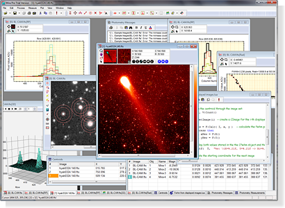
Overview
The gain of a CCD camera is the conversion between the number of electrons ("e-") recorded by the CCD and the number of digital units ("counts") contained in the CCD image. It is useful to know this conversion for evaluating the performance of the CCD camera. Since quantities in the CCD image can only be measured in units of counts, knowing the gain permits the calculation of quantities such as readout noise and full well capacity in the fundamental units of electrons. The gain value is required by some types of image deconvolution such as Maximum Entropy since, in order to correctly handle the statistical part of the calculation, the processing needs to convert the image into units of electrons. Calibrating the gain is also useful for detecting electronic problems in a CCD camera, including gain change at high or low signal level, and the existence of unexpected noise sources.
This White Paper develops the mathematical theory behind the gain calculation and shows how the mathematics suggests ways to measure the gain accurately. This note does not address the issues of basic image processing or CCD camera operation, and a basic understanding of CCD bias, dark and flat field correction is assumed.
CCD Camera Gain
The gain value is set by the electronics that read out the CCD chip. Gain is expressed in units of electrons per count. For example, a gain of 1.8 e-/count means that the camera produces 1 count for every 1.8 recorded electrons. Of course, we cannot split electrons into fractional parts, as in the case for a gain of 1.8 e-/count. What this number means is that 4/5 of the time 1 count is produced from 2 electrons, and 1/5 of the time 1 count is produced from 1 electron. This number is an average conversion ratio, based on changing large numbers of electrons into large numbers of counts. Note: This use of the term "gain" is in the opposite sense to the way a circuit designer would use the term since, in electronic design, gain is considered to be an increase in the number of output units compared with the number of input units.
It is important to note that every measurement you make in a CCD image uses units of counts. Since one camera may use a different gain than another camera, count units do not provide a straightforward comparison to be made. For example, suppose two cameras each record 24 electrons in a certain pixel. If the gain of the first camera is 2.0 and the gain of the second camera is 8.0, the same pixel would measure 12 counts in the image from the first camera and 3 counts in the image from the second camera. Without knowing the gain, comparing 12 counts against 3 counts is pretty meaningless.
Before a camera is assembled, the manufacturer can use the nominal tolerances of the electronic components to estimate the gain to within some level of uncertainty. This calculation is based on resistor values used in the gain stage of the CCD readout electronics. However, since the actual resistance is subject to component tolerances, the gain of the assembled camera may be quite different from this estimate. The actual gain can only be determined by actual performance in a gain calibration test. In addition, manufacturers sometimes do not perform an adequate gain measurement. Because of these issues, it is not unusual to find that the gain of a CCD camera differs substantially from the value quoted by the manufacturer.
Background
The signal recorded by a CCD and its conversion from units of electrons to counts can be mathematically described in a straightforward way. Understanding the mathematics validates the gain calculation technique described in the next section, and it shows why simpler techniques fail to give the correct answer.
This derivation uses the concepts of "signal" and "noise". CCD performance is usually described in terms of signal to noise ratio, or "S/N", but we shall deal with them separately here. The signal is defined as the quantity of information you measure in the image—in other words, the signal is the number of electrons recorded by the CCD or the number of counts present in the CCD image. The noise is the uncertainty in the signal. Since the photons recorded by the CCD arrive in random packets (courtesy of nature), observing the same source many times records a different number of electrons every time. This variation is a random error, or "noise" that is added to the true signal. You measure the gain of the CCD by comparing the signal level to the amount of variation in the signal. This works because the relationship between counts and electrons is different for the signal and the variance. There are two ways to make this measurement:
- Measure the signal and variation within the same region of pixels at many intensity levels.
- Measure the signal and variation in a single pixel at many intensity levels.
Both of these methods are detailed in section 6. They have the same mathematical foundation.
To derive the relationship between signal and variance in a CCD image, let us define the following quantities:
| SC | The signal measured in count units in the CCD image |
| SE | The signal recorded in electron units by the CCD chip. This quantity is unknown. |
| NC | The total noise measured in count units in the CCD image. |
| NE | The total noise in terms of recorded electrons. This quantity is unknown. |
| g | The gain, in units of electrons per count. This will be calculated. |
| RE | The readout noise of the CCD, in [electrons]. This quantity is unknown. |
| s E | The photon noise in the signal NE |
| s o | An additional noise source in the image. This is described below. |
We need an equation to relate the number of electrons, which is unknown, to quantities we measure in the CCD image in units of counts. The signals and noises are simply related through the gain factor as
These can be inverted to give
The noise is contributed by various sources. We consider these to be readout noise, RE, photon noise attributable to the nature of light,  , and some additional noise,
  , which will be shown to be important in in the following Section. Remembering that the different noise sources are independent of each other, they add in quadrature. This means that they add as the square their noise values. If we could measure the total noise in units of electrons, the various noise sources would combine in the following way:
The random arrival rate of photons controls the photon noise, . Photon noise obeys the laws of Poissonian statistics, which makes the square of the noise equal to the signal, or  . Therefore, we can make the following substitution:
Knowing how the gain relates units of electrons and counts, we can modify this equation to read as follows:
which then gives
We can rearrange this to get the final equation:
This is the equation of a line in which  is the y axis,
  is the x axis, and the slope is 1/g. The extra terms
  are grouped together for the time being. Below, they will be separated, as the extra noise term has a profound effect on the method we use to measure gain. A better way to apply this equation is to plot our measurements with as the y axis and as the x axis, as this gives the gain directly as the slope. Theoretically, at least, one could also calculate the readout noise,
  , from the point where the line hits the y axis at = 0. Knowing the gain then allows this to be converted to a Readout Noise in the standard units of electrons. However, finding the intercept of the line is not a good method, because the readout noise is a relatively small quantity and the exact path where the line passes through the y axis is subject to much uncertainty.
With the mathematics in place, we are now ready to calculate the gain. So far, I have ignored the "extra noise term", . In the next 2 sections, I will describe the nature of the extra noise term and show how it affects the way we measure the gain of a CCD camera.
Crude Estimation of the Gain
- Obtain images at different signal levels and subtract the bias from them. This is necessary because the bias level adds to the measured signal but does not contribute noise.
- Measure the signal and noise in each image. The mean and standard deviation of a region of pixels give these quantities. Square the noise value to get a variance at each signal level.
- For each image, plot Signal on the y axis against Variance on the x axis.
- Find the slope of a line through the points. The gain equals the slope.
Is measuring the gain actually this simple? Well, yes and no. If we actually make the measurement over a substantial range of signal, the data points will follow a curve rather than a line. Using the present method we will always measure a slope that is too shallow, and with it we will always underestimate the gain. Using only low signal levels, this method can give a gain value that is at least "in the ballpark" of the true value. At low signal levels, the curvature is not apparent, though present. However, the data points have some amount of scatter themselves, and without a long baseline of signal, the slope might not be well determined. The curvature in the Signal - Variance plot is caused by the extra noise term which this simple method neglects.
The following factors affect the amount of curvature we obtain:
- The color of the light source. Blue light is worse because CCD’s show the greatest surface irregularity at shorter wavelengths. These irregularities are described in Section 5.
- The fabrication technology of the CCD chip. These issues determine the relative strength of the effects described in item 1.
- The uniformity of illumination on the CCD chip.If the Illumination is not uniform, then the sloping count level inside the pixel region used to measure it inflates the measured standard deviation.
Fortunately, we can obtain the proper value by doing just a bit more work. We need to change the experiment in a way that makes the data plot as a straight line. We have to devise a way to account for the extra noise term, . If were a constant value we could combine it with the constant readout noise. We have not talked in detail about readout noise, but we have assumed that it merges together all constant noise sources that do not change with the signal level.
The Extra Noise Term in the Signal-Variance Relationship
The mysterious extra noise term, , is attributable to pixel-to-pixel variations in the sensitivity of the CCD, known as the flat field effect. The flat field effect produces a pattern of apparently "random" scatter in a CCD image. Even an exposure with infinite signal to noise ratio ("S/N") shows the flat field pattern. Despite its appearance, the pattern is not actually random because it repeats from one image to another. Changing the color of the light source changes the details of the pattern, but the pattern remains the same for all images exposed to light of the same spectral makeup. The importance of this effect is that, although the flat field variation is not a true noise, unless it is removed from the image it contributes to the noise you actually measure.
We need to characterize the noise contributed by the flat field pattern in order to determine its effect on the variance we measure in the image. This turns out to be quite simple: Since the flat field pattern is a fixed percentage of the signal, the standard deviation, or "noise" you measure from it is always proportional to the signal. For example, a pixel might be 1% less sensitive than its left neighbor, but 3% less sensitive than its right neighbor. Therefore, exposing this pixel at the 100 count level produces the following 3 signals: 101, 100, 103. However, exposing at the 10,000 count level gives these results: 10,100, 10,000, 10,300. The standard deviation for these 3 pixels is  counts for the low signal case but is
  counts for the high signal case. Thus the standard deviation is 100 times larger when the signal is also 100 times larger. We can express this proportionality between the flat field "noise" and the signal level in a simple mathematical way:
  In the present example, we have k=0.02333. Substituting this expression for the flat field variation into our master equation, we get the following result:
With a simple rearrangement of the terms, this reveals a nice quadratic function of signal:
When plotted with the Signal on the x axis, this equation describes a parabola that opens upward. Since the Signal - Variance plot is actually plotted with Signal on the y axis, we need to invert this equation to solve for SC:
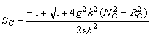
This final equation describes the classic Signal - Variance plot. In this form, the equation describes a family of horizontal parabolas that open toward the right. The strength of the flat field variation, k, determines the curvature. When k = 0, the curvature goes away and it gives the straight line relationship we desire. The curvature to the right of the line means that the stronger the flat field pattern, the more the variance is inflated at a given signal level. This result shows that it is impossible to accurately determine the gain from a Signal - Variance plot unless we know one of two things: Either 1) we know the value of k, or 2) we setup our measurements to avoid flat field effects. Option 2 is the correct strategy. Essentially, the weakness of the method described in Section 4 is that it assumes that a straight line relationship exists but ignores flat field effects.
To illustrate the effect of flat field variations, mathematical models were constructed using the equation above with parameters typical of commonly available CCD cameras. These include readout noise RE = 15e- and gain g = 2.0 e- / Count. Three models were constructed with flat field parameters k = 0, k = 0.005, and k = 0.01. Flat field variations of this order are not uncommon. These models are shown in the figure below.
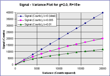
Increasing values of k correspond to progressively larger flat field irregularities in the CCD chip. The amplitude of flat field effects, k, tends to increase with shorter wavelength, particularly with thinned CCD's (this is why Section 4 recommends using a redder light source to illuminate the CCD). The flat field pattern is present in every image exposed to light. Clearly, it can be seen from the models that if one simply obtains images at different signal levels and measures the variance in them, then fitting a line through any part of the curve yields a slope lower than its true value. Thus the simple method of section 4 always underestimates the gain.
The best strategy for doing the Signal - Variance method is to find a way to produce a straight line by properly compensating for flat field effects. This is important by the "virtue of straightness": Deviation from a straight line is completely unambiguous and easy to detect. It avoids the issue of how much curvature is attributable to what cause. The electronic design of a CCD camera is quite complex, and problems can occur, such as gain change at different signal levels or unexplained extra noise at high or low signal levels. Using a "robust" method for calculating gain, any significant deviation from a line is a diagnostic of possible problems in the camera electronics. Two such methods are described in the following section.
In previous sections, the so-called simple method of estimating the gain was shown to be an oversimplification. Specifically, it produces a Signal - Variance plot with a curved relationship resulting from flat field effects. This section presents two robust methods that correct the flat field effects in the Signal - Variance relationship to yield the desired straight-line relationship. This permits an accurate gain value to be calculated. Adjusting the method to remove flat field effects is a better strategy than either to attempt to use a low signal level where flat field effects are believed not to be important or to attempt to measure and compensate for the flat field parameter k.
When applying the robust methods described below, one must consider some procedural issues that apply to both:
Both methods measure sets of 2 or more images at each signal level. An image set is defined as 2 or more successive images taken under the same illumination conditions. To obtain various signal levels, it is better to change the intensity received by the CCD than to change the exposure time. This may be achieved either by varying the light source intensity or by altering the amount of light passing into the camera. The illumination received by the CCD should not vary too much within a set of images, but it does not have to be truly constant.
- Cool the CCD camera to reduce the dark current to as low as possible. This prevents you from having to subtract dark frames from the images (doing so adds noise, which adversely affects the noise measurements at low signal level). In addition, if the bias varies from one frame to another, be sure to subtract a bias value from every image.
- The CCD should be illuminated the same way for all images within a set. Irregularities in illumination within a set are automatically removed by the image processing methods used in the calibration. It does not matter if the illumination pattern changes when you change the intensity level for a different image set.
- Within an image set, variation in the light intensity is corrected by normalizing the images so that they have the same average signal within the same pixel region. The process of normalizing multiplies the image by an appropriate constant value so that its mean value within the pixel region matches that of other images in the same set. Multiplying by a constant value does not affect the signal to noise ratio or the flat field structure of the image.
- Do not estimate the CCD camera's readout noise by calculating the noise value at zero signal. This is the square root of the variance where the gain line intercepts the y axis. Especially do not use this value if bias is not subtracted from every frame. To calculate the readout noise, use the "Two Bias" method and apply the gain value determined from this test. In the Two Bias Method, 2 bias frames are taken in succession and then subtracted from each other. Measure the standard deviation inside a region of, say 100x100 pixels and divide by 1.4142. This gives the readout noise in units of counts. Multiply this by the gain factor to get the Readout Noise in units of electrons. If bias frames are not available, cool the camera and obtain two dark frames of minimum exposure, then apply the Two Bias Method to them.
Method 1: Correct the flat field effects at each signal level
In this strategy, the flat field effects are removed by subtracting one image from another at each signal level. Here is the recipe:
For each intensity level, do the following:
- Obtain 2 images in succession at the same light level. Call these images A and B.
- Subtract the bias level from both images. Keep the exposure short so that the dark current is negligibly small. If the dark current is large, you should also remove it from both frames.
- Measure the mean signal level S in a region of pixels on images A and B. Call these mean signals SA and SB. It is best if the bounds of the region change as little as possible from one image to the next. The region might be as small as 50x50 to 100x100 pixels but should not contain obvious defects such as cosmic ray hits, dead pixels, etc.
- Calculate the ratio of the mean signal levels as r = SA / SB.
- Multiply image B by the number r. This corrects image B to the same signal level as image A without affecting its noise structure or flat field variation.
- Subtract image B from image A. The flat field effects present in both images should be cancelled to within the random errors.
- Measure the standard deviation over the same pixel region you used in step 3. Square this number to get the Variance. In addition, divide the resulting variance by 2.0 to correct for the fact that the variance is doubled when you subtract one similar image from another.
- Use the Signal from step 3 and the Variance from step 7 to add a data point to your Signal - Variance plot.
- Change the light intensity and repeat steps 1 through 8.
Method 2: Avoid flat field effects using one pixel in many images.
This strategy avoids the flat field variation by considering how a single pixel varies among many images. Since the variance is calculated from a single pixel many times, rather than from a collection of different pixels, there is no flat field variation.
To calculate the variance at a given signal level, you obtain many frames, measure the same pixel in each frame, and calculate the variance among this set of values. One problem with this method is that the variance itself is subject to random errors and is only an estimate of the true value. To obtain a reliable variance, you must use 100’s of images at each intensity level. This is completely analogous to measuring the variance over a moderate sized pixel region in Method A; in both methods, using many pixels to compute the variance gives a more statistically sound value. Another limitation of this method is that it either requires a perfectly stable light source or you have to compensate for light source variation by adjusting each image to the same average signal level before measuring its pixel. Altogether, the method requires a large number of images and a lot of processing. For this reason, Method A is preferred. In any case, here is the recipe:
Select a pixel to measure at the same location in every image. Always measure the same pixel in every image at every signal level.
For each intensity level, do the following:
- Obtain at least 100 images in succession at the same light level. Call the first image A and the remaining images i. Since you are interested in a single pixel, the images may be small, of order 100x100 pixels.
- Subtract the bias level from each image. Keep the exposure short so that the dark is negligibly small. If the dark current is large, you should also remove it from every frame.
- Measure the mean signal level S in a rectangular region of pixels on image A. Measure the same quantity in each of the remaining images. The measuring region might be as small as 50x50 to 100x100 pixels and should be centered on the brightest part of the image.
- For each image Si other than the first, calculate the ratio of its mean signal level to that of image A. This gives a number for each image, ri = SA / Si.
- Multiply each image i by the number ri. This corrects each image to the same average intensity as image A.
- Measure the number of counts in the selected pixel in every one of the images. From these numbers, compute a mean count and standard deviation. Square the standard deviation to get the variance.
- Use the Signal and Variance from step 6 to add a data point to your Signal - Variance plot.
- Change the light intensity and repeat steps 1 through 7.
Summary
We have derived the mathematical relationship between Signal and Variance in a CCD image which includes the pixel-to-pixel response variations among the image pixels. This "flat field" effect must be compensated or the calculated value of the camera gain will be incorrect. We have shown how the traditional "simple" method used for gain calculation leads to an erroneous gain value unless flat field effects are not considered. We have suggested 2 methods that correctly account for the flat field effect, and these should be implemented in camera testing procedures.
E. XO CONTOUR PLOTTING WITH MIRA
_____________________________________________________
 Contour plots show levels of constant intensity or luminance in an image, much like a topographic map. With Mira, there is no limit to the size of image, or the data type (8 to 64 bits per pixel). Up to 100 levels may be contoured in multi-contour mode or you can "click to contour" at a single curve at a target luminance level. Adjustable contour stiffness selects between showing full detail and excluding noise — essential for analyzing low S/N data. You can adjust the number of contours, change the colors, and choose auto-levels or contours at specific levels of your choice. 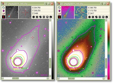 These examples show contours plotted on a grayscale image before and after applying a pseudo-color palette enhancement. Notice how the contour tracks luminance changes revealed so well by the pseudo-color palette. However, they don't show exactly the same thing. Contours trace through luminance values at the sub-pixel level, considering neighboring values, whereas palettes select only the pixel values as literally defined in the image. These examples show contours plotted on a grayscale image before and after applying a pseudo-color palette enhancement. Notice how the contour tracks luminance changes revealed so well by the pseudo-color palette. However, they don't show exactly the same thing. Contours trace through luminance values at the sub-pixel level, considering neighboring values, whereas palettes select only the pixel values as literally defined in the image. |
Adjusting Contour Stiffness, or "Smoothing"These examples show a single contour at a luminance level near the background. Since it has a very low Signal to Noise Ratio, the contour is subject to tracking noise. Mira allows you to select the stiffness of the contour following algorithm to trace fine details in high SNR data or coarse details in low SNR data.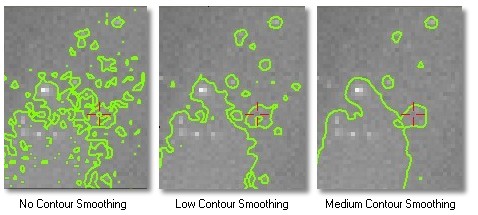 |
Mira Contour Tools
These dialogs show how you create contours to meet your needs. The left dialog controls multiple contours as shown in the first example, above. The right dialog controls generation of single, interactive contours.
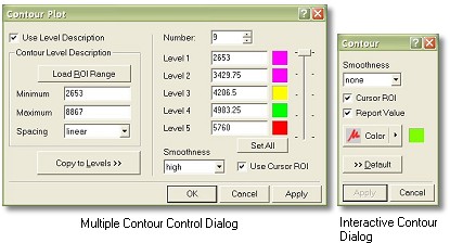 |
3-D Visualization of Image Data
 Mira MX x64, Mira Pro x64, and Mira Pro Ultimate Edition have an integrated 3-D viewer that renders 2-D images in 3-D, providing additional opportunities for inspecting and analyzing both images and model data. This Brief illustrates some of the variations possible for visualizing image data using Mira MX x64.
Mira's 3-D plotting tool renders rectangular regions of 2-D images of any size and with bit depths from 8 to 64 bits per pixel, integer or real data type (not RGB). And it works with image stacks too. With the Mira Pro x64, Mira Pro UE, and Mira MX x64, a single button click can also render a region of an image stack of any depth, such as 10, 100, or even more images. You can animate them, rotate, tilt, adjust the palette, or change Z-axis scaling on the fly.
Mira Pro x64, Mira Pro UE, and Mira MX x64 provide a combination of 4 plot types with 6 pixel representations (Mira Pro has 2 representations). Combine these options with illumination changes, Mira's exceptional palette manipulation, and you get many more variations than are shown below.
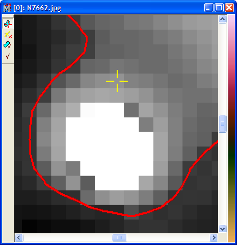 | 2-D Image
This 2-D image shows an extreme enlargement of an image displayed by Mira. The red curve shows a contour of constant value computed by Mira. The contour gives the user some additional information about the shape of the profile. Multiple contours could have been computed at various values to give even more information. Still, there are other ways to look at the object using 3-D rendering.
|
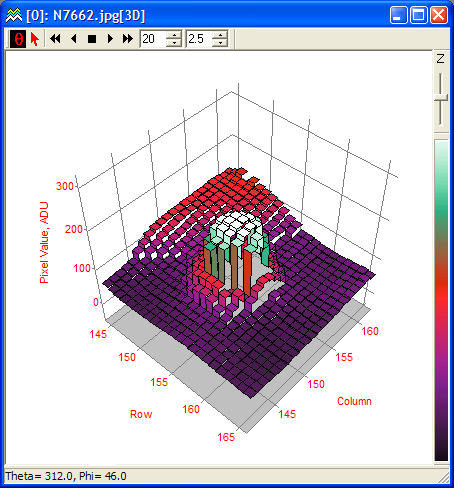 | Stepped Ribbon Plot
This 3-D view shows the region of the 2-D image shown above. Here, we show an intensity surface plot with a stepped ribbon pixel representation. The intensity surface maps the data Z-value to a palette entry. The stepped ribbon representation gives the data pixels a flat top but provide some transparency for viewing through the rendered data. The palette was changed from grayscale to one of the stock pseudo color palettes to more clearly distinguish changes in Z value. This plot is rotated 48� counterclockwise relative to the 2-D image.
|
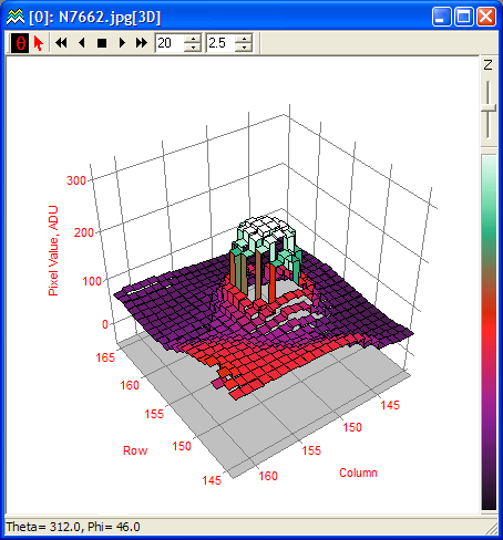 | Stepped Ribbon Plot, Rotated in Azimuth
This view shows the same stepped ribbon plot as above, but the viewpoint has been rotated around to the opposite side. 3-D rotation in Mira is dynamic, using mouse movement to tilt or rotate the rendering in real-time.
|
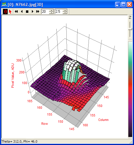 | Standard Ribbon Plot
This plot is similar to the stepped ribbon except that it connects pixel values at their center rather than at their edges. The plot type was changed to one of numerous options by clicking a bullet on a Mira dialog.
|
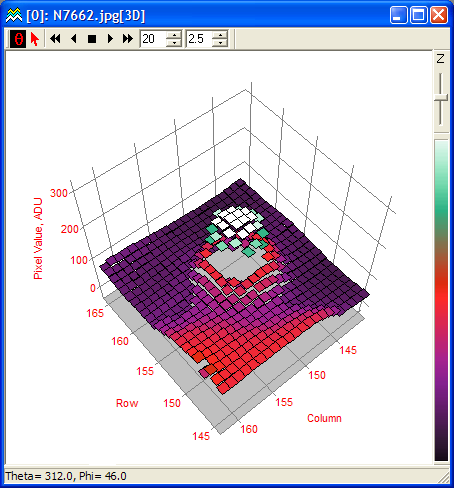 | Pixel Plot
In this view, the pixel representation was changed to pixel, which plots the pixel value as a constant-Z surface while removing all sides facets. The advantage of this representation is that the plot is maximally transparent while still showing the Z-value of the data.
|
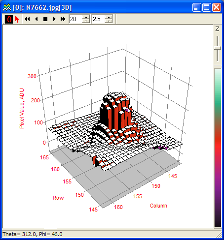 | Illuminated Surface with Pedestal Representation
For this view, the plot type was changed from intensity surface to illuminated surface and the pixel representation was changed from ribbon to pedestal. The illuminated surface plot uses a light source and Phong Shading to recreate a visible surface. All the Phong parameters are adjustable, in real-time.
|
Source Extraction
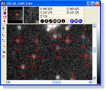
Source Extraction is also known by the names "image segmentation" and "image labeling" in various applications. This procedure identifies, or detects individual objects or image features in one or more images and computes some 40 properties for each detection. Source Extraction provides numerous options for controlling the detection and processing of information. The procedure may also be used to detect objects or features that are common to an image set or that vary among the images. Source extraction is handled using the Source Extraction package in Mira MX x64, Mira Pro x64, and Mira Pro Ultimate Edition.
This tutorial, from the Mira User's Guide, shows how use the MExtract package ro perform image source extraction. The MExtract tool is accessed using the Measure > Extract Sources command and works with the currently top-most Image Window. This tutorial examines the FWHM values for many stars in a small region of an astronomical image. Although this presents is an astronomy application, the MExtract package is widely used for abroad variety of applications. This tutorial does not describe the Match and Difference methods which detect sources that are common to, or different among, a set of images.
Overview
Source extraction processing uses a chain of operations called a "pipeline". Each step in the pipeline involves preferences that control its operation. Because Mira allows so many variations for the steps used in the pipeline, a Profile control is used to manage the procedure. The pipeline is operated from the Source Extraction Dialog. After you have choose a profile or set your preferences, you run the pipeline by clicking the [Process] button.
The source extraction pipeline involves a procedure formed from the steps you select. Each of these steps is optional but those you select are applied in a specific order, hence the term "pipeline" to describe a single direction of "flow" in the processing. The first step in source extraction involves determination of the background level. Knowing the background at each point, each pixel can be tested against the threshold above background; if the pixel exceeds the threshold, it is tagged as a source candidate. All candidate pixels are then collected into objects completely separated from others by a boundary at the specified threshold level. In this way, the sources are like islands poking above sea level. Source properties such as luminance, ellipticity, area, and others are then computed. The final processing step involves filtering this source list to retain only the sources that meet criteria such as being within a certain range of area or ellipticity. The list of sources extracted from the image(s) may then be further analyzed using Mira tools or saved for analysis by other software. [ View measured parameters ]
Getting Started
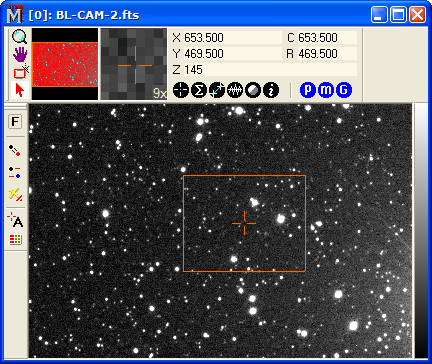 To begin, use the File > Open command to load theOpen dialog. As shown below, select the sample imageBL-CAM-2.fts and click [Open] to display it in Mira.
After opening the image, click the Measure > Extract Sources command in the pull-down menu. This opens the Source Extraction Toolbar which operates all the commands of the Source Extraction package. As typical in Mira, the toolbar opens on the left border of the image window with marking mode active:
 The toolbar commands are described below. In this tutorial, the only buttons you will use are the first and last ones:
Notice that there is no marking mode on this toolbar. This is different from the way most command toolbars work because source extraction does not involve any interactive marking modes. Rather than clicking on sources using the mouse, source extraction automatically finds the objects for you.
Loading the Tutorial Preferences
 Next, you will load the extraction preferences to be used in this tutorial. On the toolbar, click the
When the profile is loaded, Mira sets all the preferences on on all dialog pages to those values stored in the profile. To see what all dialogs should look like for this tutorial, click here. Note that, in this tutorial, you will not be using the Multiple Images options (Match and Difference) because only a single image has been loaded. If you double click on Multiple Images to open its options, you will see all options disabled with X marks. As a consequence, the preferences on the Match and Diff pages are not used.
Running the Extraction Pipeline
Next, you will run the pipeline using the "Tutorial" profile. With the Source Extraction pipeline dialog open, click[Process]. After some number of seconds, the pipeline finishes and the Source Extraction Messageswindow opens as shown below:
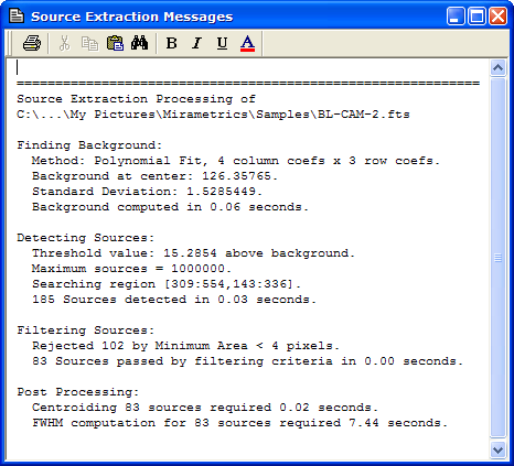
The Messages window was created because the Verbose box was checked on the Procedure page. This is a standard Mira Text Editor window, so the results listed here can be edited or saved for your records.
There are a number of things to be learned from the Messages window. The first interesting point is that 185 sources were identified inside the rectangular region of the image cursor but setting a minimum area of 4 pixels discarded 102 of them, leaving 83 sources 4 pixels or larger. At this low threshold above background, we detected quite a few hot pixels very small object which are mostly just warm pixels You could verify this by re-running the pipeline after un-checking Min Area and setting Max Area = 2 pixels on the Filter page. Second, the Finding, Detecting, and Filtering steps required a very small amount of time to complete, but it took approximately 100 times as long to compute the Precision FWHM values in the Post Processing step. Therefore, if you re-run the pipeline to count the number of tiny bumps, the "computationally expensive" FWHM step is not necessary and should be turned off.
Since the Label step was checked in the procedure, the result of the extraction pipeline looks like the image below, with the final sources marked and tagged with a number. This image was zoomed 2x to give better separation between markers.
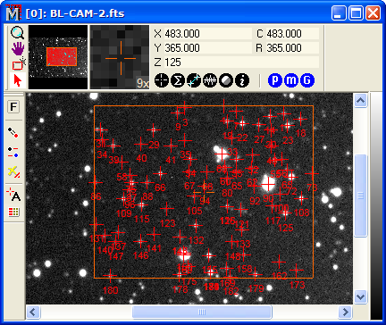 Using the magnify mode or your mouse thumbwheel, zoom the image to 4x so it looks like the picture below, left. You can now see the kinds of sources that were detected. Notice how bright the faintest objects are compared with the sky noise. This makes it apparent how well Mira's centroiding algorithm works for faint sources. Look at object 68 in particular.
Since we selected Report Method = "No Report" on the Procedure page, the source properties extracted from BL-CAM-2.fts were not listed anywhere. Choosing not to display the results can save time if a large number of objects are detected, especially if you do not know if you want to  save them (Hint: You can maximize the scrolling speed of the report window by keeping Auto-optimizing the column widths). However, you can view the information after the fact. In this case, only 83 sources passed the filtering and that is quick to display in a Report window. Click
  to open the Source Extraction dialog and select the Procedure page. Click the [List] button and a Report window opens as in the picture below (this is shown scrolled down to object 66). Close the Preferences dialog so you can continue using the other windows.
 save them (Hint: You can maximize the scrolling speed of the report window by keeping Auto-optimizing the column widths). However, you can view the information after the fact. In this case, only 83 sources passed the filtering and that is quick to display in a Report window. Click
If you want to save these results, make sure the Report window is top-most and use the File > Save As command to save it to a text file.
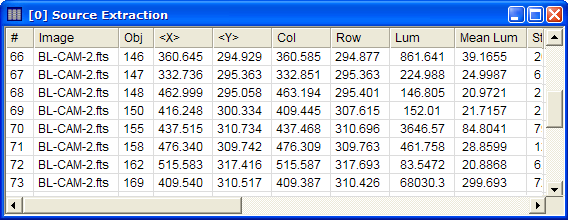 command to save it to a text file.
Analyzing the Extraction Data
You can do many things with the tabular data in a Report window, including save it to a text file, copying onto the Windows Clipboard, or rearranging the columns and sorting the rows to make comparisons (see Arranging Report Data). In addition, you can create a Scatter Plot to examine relationships between the source properties.
Make the Source Extraction Report the top-most window and click the View > Scatter Plot command in the pull-down menu. You can also access commands like Scatter Plot by right-clicking inside the Report window to open it Context Menu. The Scatter Plot command opens a setup dialog like this one:
In the Scatter Plot dialog, you select which columns of report data to plot on the horizontal and vertical axes. Optionally, you can also set a title and select columns containing data to be used as error bars. As shown above, use the two left-hand list boxes to select "Lum" as the X Axis Variable and "FWHM" as the Y Axis Variable. This will produce a graph showing FWHM versus Luminance for all the sources that were extracted from the BL-CAM-2.fts image. Click [Plot] to create the graph like this:
Notice that a single point with FWHM near 600 has set the plot scale so that the other points are all crunched together near the bottom. We will investigate this particular source later. At the moment, let's have a closer look at the other FWHM values. On the Plot Toolbar, Click  to enter Expand Mode and drag a rubber band around the plot region to zoom in as shown at left.
We can see that the typical FWHM is around 3.2 pixels. The increased scatter in FWHM at very low luminance is to be expected because the measurement becomes dominated by sky noise. The higher values of FWHM could be faint galaxies or could just be random fluctuations for very faint stars. We can examine them more closely using the same method we will use for the object we noted above as having a FWHM near 600. Which object is that? You could scroll through the table to find it but there is an easier way. In the Report window, click the FWHM column header to sort the source list by value. If it sorts in the wrong sense, with the smallest value at the top of the list, click again to get the largest value at the top of the list. Right-click on the cell containing the value FWHM value of 577 to open the Context Menu for this Report window. Notice that the value highlights underneath the menu as shown below, left. In the menu, selectGo To Object as shown here:
 higher values of FWHM could be faint galaxies or could just be random fluctuations for very faint stars. We can examine them more closely using the same method we will use for the object we noted above as having a FWHM near 600. Which object is that? You could scroll through the table to find it but there is an easier way. In the Report window, click the FWHM column header to sort the source list by value. If it sorts in the wrong sense, with the smallest value at the top of the list, click again to get the largest value at the top of the list. Right-click on the cell containing the value FWHM value of 577 to open the Context Menu for this Report window. Notice that the value highlights underneath the menu as shown below, left. In the menu, selectGo To Object as shown here:
The Go To Object command shifts the displayed image to the position of the object who's table cell was highlighted. If you expose the Image Window containing BL-CAM-2.fts, you will see it centered as shown below. The zoom value was set on the Procedure page of the Source Extraction dialog.
Why did Mira calculate a FWHM value of 577 for this object? To answer that question, click the  button on the left end of the Image Toolbar to enter Roam Mode (so that clicking on the image does not execute any command from a toolbar).
  Now hold down the Shift key and click the mouse pointer on the star to center the Image Cursor at that point. Then click the
  button on the main toolbar to create a Radial Profile Plot like the one shown at left, below.
 Now hold down the Shift key and click the mouse pointer on the star to center the Image Cursor at that point. Then click the
The object of interest is on the left, centered at a radius value of 0. The huge scatter of points on the right correspond to the extremely bright star just above the target star in the Image Window. Notice the FWHM value of 1037 pixels listed in the caption above the plot box. It is clear that the FWHM measurement could not cope with the  extremely bright star in the nearby background, which made the measurement invalid.
 extremely bright star in the nearby background, which made the measurement invalid.
There is another object of interest in this report window. If you sort the FWHM list again, the object at the small end has the value -1.#IND, which is computer speak for a numerical value that could not be computed. Usually this means that the object is just too faint to get a numerically stable solution for the FWHM. Right-click on this value and repeat the Go To Object command as shown in the left picture, below. The Go To Object command centers the Image Window on the point as shown in the right picture, below.

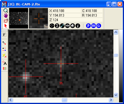 That is one really faint object. Again, the FWHM value could not be calculated because the object was just so faint that the solution gave a nonsensical result. Still, the centroid coordinate appears to be accurate even at this incredibly low brightness level.
1-D Data Visualization in Mira
 This Brief describes the various types plots that can be created by Mira for visualizing 1-D data (also see the 1-d Fit package built into Mira MX x64). Mira's 1-D plotting architecture was designed to efficiently and effectively work with data sets consisting of many points, many images, and many series. Mira can create representations like step-line plots and x/y error bars. Plots can also be printed on any printer supported by Windows to obtain publication-quality hardcopy.
Although most plots are made from data in an Image window, plots can also be generated from tabular measurements and by using the extensive and versatile collection of plotting functions in the scripting module. Not discussed here are topics like scripted plots, working with plot data, plot commands, toolbars, plot attributes, etc.
Plot Types
The table below describes plotting capabilities of various Mira platforms. Not all features are in all platforms, and such cases are noted. Pictures...
Column Profile | Plots the intensity of a single column or all columns in a region of interest, for 1 image or an image stack. The single column intensity may also be the mean, median, or sum of all columns in the region of interest. |
Row Profile | Plots the intensity of a single row or all rows in a region of interest, for 1 image or an image stack. The single row intensity may also be the mean, median, or sum of all rows in the region of interest. |
Line Profile |
Plots the intensity along a drawn line between two points. Optionally, the starting or ending point may be auto-centroided to the moment-weighted local maximum or minimum sub-pixel position. Additional intensity series may be added to the plot using lines exactly parallel to or displaced from the first line.
|
Radial Profile Plot | Plots the radial intensity profile in all directions from a sub-pixel positioned center point. Optionally, the center point may be auto-centroided to the moment-weighted local maximum or minimum sub-pixel position. Optionally, a Gaussian + Constant model may be fit to the sample data and the results reported for estimation of FWHM, Peak intensity, and background luminance. |
Histogram Plot | Shows the frequency distribution of image values inside a region of interest. The plot may be made for one image or an entire image stack may be plotted on the same set of axes. |
Bit Histogram Plot | Plots the frequency of bit values inside a region of interest. The plot may be drawn for one image or an image stack. (Mira Pro and Mira MX) |
Scatter Plot | Plots discrete points from tables containing measurement results. The columns to plot are selected from the table. (Mira MX) |
Pixel Series Plot | Plots multiple plot series showing the pixel value at a given location for the members of an image stack. (Mira Pro and Mira MX). |
Custom Plots | Plots can also be generated by the MX Script and Pro Script modules. In addition to the plot types above, scripted plots may contain any number of points in any number of series with any combination of lines, points, error bars, colors, attributes, etc. |
Data Fitting | Mira MX provides an outstanding tool for analyzing 1-dimensional data using polynomial regression. Features include iterative sigma clipping, forced coefficient values, selectable data series, auto-rejection, manual deletion and weighting, and more. More |
Examples
 | A Simple Plot
This shows a simple plot along a single column of an image. The Plot Toolbar (at the top of the window in other pictures, below), is disabled in this view.
|
 | Overplot of Column Intensity Plots from 5 Images
The Image Window displayed a stack of 5 images. A single button click plotted the same column in each image. The colors assigned to the 5 plot series can be specified. At the top of the window is shown the Plot Toolbar provided with Mira Pro.
|
 | Animating the 5 Column Plots (from above)
Using the same data as above, the Plot Windows was switched to Animate mode. This shows 1 plot series at a time which can be stepped, selected, or animated in various ways. At the top of the window is shown the Plot Toolbar provided with Mira MX.
|
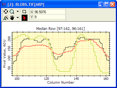 | Comparing Plots on the Same Axes (Mira Pro and MX)
Separate plots were created for a single row slice, a median row slice and a mean row slice (each in a different window). The Single Row and Median Row plots were appended to the Mean Row plot using the plot copy+paste commands in Mira Pro and Mira MX.
|
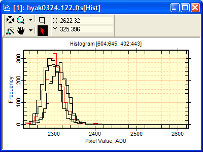 | Comparing Histograms of several images (Mira Pro and MX)
This example plots the histogram of the same region of interest in 5 images. The images were opened as an image stack, then the histogram plot button clicked once. All plots were originally drawn in black. The plot for image 2 was changed to red as a reference for comparison with the other histograms. [Changing attributes of individual plot series is a feature of Mira MX.]
|
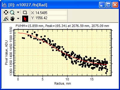 | Radial Profile Plot with Fit
This example shows a standard Mira feature of all platforms: the radial profile plot. This type of plot is important for characterizing the point spread function of an image. Optionally, a Gaussian + Constant model is fit to the data and is used to estimate the FWHM, Background, and Peak value of the profile data. Even with very low signal to noise ratio data, as shown here, Mira's fit is robust and the estimated parameters are accurate. In addition, the visual drawing of the fit through the data provides an unambiguous check on the validity of the estimated parameters.
|
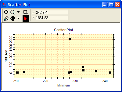 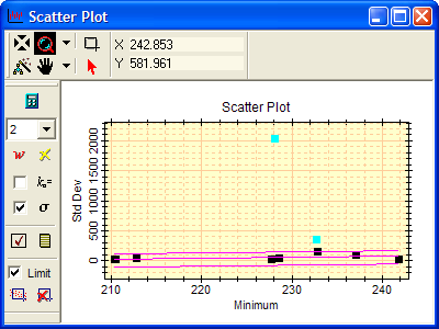 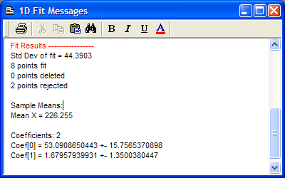 | Scatter Plot with Polynomial Fit (Mira MX)
This example shows the result of making, plotting, and performing regression analysis on the results of image measurements. Staring with a table of measurements, 6 button clicks and about 10 seconds selected and plotted the target data columns and produced the regression results.
|
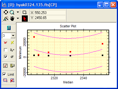 | Scatter Plot with Polynomial Fit (Mira MX)
This example shows a scatter plot with a 3-term polynomial fit. The data were generated by a script that computed the regional minimum value from several images. The script created and populated the Plot Window. After the script terminated, in Mira MX, the 1d-Fit toolbar was opened and the fit computed interactively on the data. This fit uses iterative sigma clipping. The upper and lower purple curves show 3 sigma deviations from the fit, which shows no points rejected. The black and red points show two different plot series resulting from the two groups of images being compared.
|
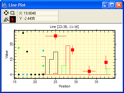 | Custom Plot Created by a Script
This illustrates the versatility of plots generated by Mira scripts module. This plot mixes points symbols, step-lines, x and x-y error bars, etc.

+++++++++++++++++++++++++++++++++
e- Light and Contour to Landscape

+++++++++++++++++++++++++++++++++++++
|