


Time Switch
The figure A depicts concept of time switch.
As shown it is basically a time slot interchanger (ISI). A time slot in PCM consists of 8 bits and represents 1 voice channel. The time slot is repeated 8000 times in a second. DS1 has 24 time slots in a frame and E1 has 32 time slots in a frame.
As shown in the figure A , connectivity is established between user-C on slot-C to user-G on Slot-G. In order to perform time switch operation following steps are needed:
• Memory to store time slot speech data to write and to read at the output for changing the position.
• Memory to store control action to be performed on the stored data.
• Time slot counter or processor.
Space Switch
Figure-B depicts time division space switch. It consists of cross point matrix made up of logic gates which allow switching of time slots in spatial domain. There will be input horizontals and output verticals with logic gate at each of the crosspoints of the space switch.
A tandem switching centre, or the route switch of a local exchange must be able to connect any channel on one of its incoming PCM highways to any channel of an outgoing PCM highway. The incoming and outgoing highways are spatially separate. Hence connection here need space switch.

In general, a connection will occupy different time slots on the incoming and outgoing highways. Hence switching network must be able to receive PCM samples from one time slot and re-transmit them in a different time slot. This is referred as time slot interchange or simple time switching.
Figure mentions the data transmitted on time slot no. 1 and 2 are later transmitted on time slot no. 24 of stream A and stream B at the output. Consequently, switching network of a tandem exchange or route switch of a local exchange must perform both time switching as well as space switching.
Space switch is like matrix of N x M physical lines. Time switch is like memory having data at its different consecutive address locations.
The switching scheme used by the electronic switching systems may be either Space Division Switching or Time Division Switching. In space division switching, a dedicated path is established between the calling and the called subscribers for the entire duration of the call. In time division switching, sampled values of speech signals are transferred at fixed intervals.
The time division switching may be analog or digital. In analog switching, the sampled voltage levels are transmitted as they are whereas in binary switching, they are binary coded and transmitted. If the coded values are transferred during the same time interval from input to output, the technique is called Space Switching. If the values are stored and transferred to the output at a late time interval, the technique is called as Time Switching. A time division digital switch may also be designed by using a combination of space and time switching techniques.
Space Division Switching
The paths in a circuit are separated from each other, spatially in space division switching. Though initially designed for analog networks, it is being used for both analog and digital switching. A Cross point switch is mostly referred to as a space division switch because it moves a bit stream from one circuit or bus to another.
The switching system where any channel of one of its incoming PCM highway is connected to any channel of an outgoing PCM highway, where both of them are spatially separated is called the Space Division Switching. The Cross point matrix connects the incoming and outgoing PCM highways, where different channels of an incoming PCM frame may need to be switched by different Cross points in order to reach different destinations.
Though the space division switching was developed for the analog environment, it has been carried over to digital communication as well. This requires separate physical path for each signal connection, and uses metallic or semiconductor gates.

In electronics and especially synchronous digital circuits, a clock signal (historically also known as logic beat ) oscillates between a high and a low state and is used like a metronome to coordinate actions of digital circuits.
A clock signal is produced by a clock generator. Although more complex arrangements are used, the most common clock signal is in the form of a square wave with a 50% duty cycle, usually with a fixed, constant frequency. Circuits using the clock signal for synchronization may become active at either the rising edge, falling edge, or, in the case of double data rate, both in the rising and in the falling edges of the clock cycle.

Interfacing is the method of connecting or linking together one device, especially a computer or micro-controller with another allowing us to design or adapt the output and input configurations of the two electronic devices so that they can work together.
But interfacing is more than just using the software program of computers and processors to control something. While computer interfacing uses the unidirectional and bidirectional input and output ports to drive various peripheral devices, many simple electronic circuits can be used to interface to the real world either using mechanical switches as inputs, or individual LEDs as outputs.

Pushbutton Switch
For an electronic or micro-electronic circuit to be useful and effective, it has to interface with something. Input interface circuits connect electronic circuits such as op-amps, logic gates, etc. to the outside world expanding its capabilities.
Electronic circuits amplify, buffer or process signals from sensors or switches as input information or to control lamps, relays or actuators for output control. Either way, input interfacing circuits convert the voltage and current output of one circuit to the equivalent of another.
Input sensors provide an input for information about an environment. Physical quantities such as temperature, pressure or position that vary slowly or continuously with time can be measured using various sensors and switching devices giving an output signal relative to the physical quantity being measured.
Many of the sensors that we can use in our electronic circuits and projects are resistive in that their resistance changes with the measured quantity. For example, thermistors, strain gauges or light dependant resistors (LDR). These devices are all classed as input devices.
Input Interfacing Circuits
The simplest and most common type of input interfacing device is the push button switch. Mechanical ON-OFF toggle switches, push-button switches, rocker switches, key switches and reed switches, etc. are all popular as input devices because of their low cost and easy of input interfacing to any circuit. Also the operator can change the state of an input simply by operating a switch, pressing a button or moving a magnet over a reed switch.
Input Interfacing A Single Switch

Switches and push-buttons are mechanical devices that have two or more sets of electrical contacts. When the switch is open or disconnected, the contacts are open circuited and when the switch is closed or operated these contacts are shorted together.
The most common way of input interfacing a switch (or push button) to an electronic circuit is via a pull-up resistor to the supply voltage as shown. When the switch is open, 5 volts, or a logic “1” is given as the output signal. When the switch is closed the output is grounded and 0v, or a logic “0” is given as the output.
Then depending upon the position of the switch, a “high” or a “low” output is produced. A pull-up resistor is necessary to hold the output voltage level at the required value (in this example, +5v) when the switch is open and also to prevent the switch from shorting out the supply when closed.
The size of the pull-up resistor depends on the circuit current when the switch is open. For example, with the switch open, current will flow down through the resistor to the VOUT terminal and from Ohms Law this flow of current will cause a voltage drop to appear across the resistor.
Then if we assume a digital logic TTL gate requires an input “HIGH” current of 60 micro-amps (60uA), this causes a voltage drop across the resistor of: 60uA x 10kΩ = 0.6V, producing an input “HIGH” voltage of 5.0 - 0.6 = 4.4V which is well within the input specifications of a standard digital TTL gate.
A switch or push-button can also be connected in “active high” mode where the switch and resistor are reversed so that the switch is connected between the +5V supply voltage and the output. The resistor, which is now known as a pull-down resistor, is connected between the output and the 0v ground. In this configuration when the switch is open, the output signal, VOUT is at 0v, or logic “0”. When the witch is operated the output goes “HIGH” to the +5 volts supply voltage or logic “1”.
Unlike the pull-up resistor which is used to limit the current, the main purpose of a pull-down resistor is to keep the output terminal, VOUT from floating about by tying it to 0v or ground. As result a much smaller resistor can be used as the voltage drop across it will usually be very small. However, using a too small a pull-down resistor value will result in high currents and high power dissipation in the resistor when the switch is closed or operated.
DIP Switch Input Interfacing

As well as input interfacing individual push-buttons and rocker switches to circuits, we can also interface several switches together in the form of keypads and DIP switches.
DIP or Dual-in-line Package switches are individual switches that are grouped together as four or eight switches within a single package. This allows DIP switches to be inserted into standard IC sockets or wired directly onto a circuit or breadboard.
Each switch within a DIP switch package normally indicates one of two conditions by its ON-OFF status and a four switch DIP package will have four outputs as shown. Both slide and rotary type DIP switches can be connected together or in combinations of two or three switches which makes input interfacing them to a wide range of circuits very easy.
Mechanical switches are popular because of their low cost and ease of input interfacing. However, mechanical switches have a common problem called “contact bounce”. Mechanical switches consist of two pieces of metal contacts which are pushed together to complete a circuit when you operate the switch. But instead of producing a single clean switching action, the metal parts touch and bounce together inside the body of the switch causing the switching mechanism to open and close several times very quickly.
Because the mechanical switch contacts are designed to open and close quickly, there is very little resistance, called damping to stop the contacts from bouncing about as they make or break. The result is that this bouncing action produces a series of pulses or voltage spikes before the switch makes a solid contact.
Switch Bounce Waveform

The problem is that any electronic or digital circuit which the mechanical switch is input interfaced too could read these multiple switch operations as a series of ON and OFF signals lasting several milliseconds instead of just the one intended single and positive switching action.
This multiple switch closing (or opening) action is called Switch Bounce in switches with the same action being called Contact Bounce in relays. Also, as switch and contact bounce occurs during both the opening and closing actions, the resultant bouncing and arcing across the contacts causes wear, increases contact resistance, and lowers the working life of the switch.
However, there are several ways in which we can solve this problem of switch bounce by using some extra circuitry in the form of a debounce circuit to “de-bounce” the input signal. The easiest and most simplest way is to create an RC debounce circuit that allows the switch to charge and discharge a capacitor as shown.
RC Switch Debounce Circuit

With the addition of an extra 100Ω resistor and a 1uF capacitor to the switches input interfacing circuit, the problems of switch bounce can be filtered out. The RC time constant, T is chosen to be longer than the bounce time of the mechanical switching action. An inverting Schmitt-trigger buffer can also be used to produce a sharp output transition from LOW to HIGH, and from HIGH to LOW.
So how does this type of input interfacing circuit work?. Well we saw in the RC Charging tutorial that a capacitor charges up at a rate determined by its time constant, T. This time constant value is measured in terms of T = R*C, in seconds, where R is the value of the resistor in Ohms and C is the value of the capacitor in Farads. This then forms the basis of an RC time constant.
Lets first assume that the switch is closed and the capacitor is fully discharged, then the input to the inverter is LOW and its output is HIGH. When the switch is opened, the capacitor charges up via the two resistors, R1 and R2 at a rate determined by the C(R1+R2) time constant of the RC network.
As the capacitor charges up slowly, any bouncing of the switch contacts are smoothed out by the voltage across the capacitors plates. When the charge on the plates is equal too or greater than the lowest value of the upper input voltage ( VIH ) of the inverter, the inverter changes state and the output becomes LOW. In this simple switch input interfacing example, the RC value is about 10mS giving the switch contacts enough time to settle into their final open state.
When the switch is closed, the now fully charged capacitor will quickly discharge to zero through the 100Ω at a rate determined by the C(R2) time constant changing the state of the inverters output from LOW to HIGH. However, the operation of the switch causes the contacts to bounce about resulting in the capacitor wanting to repeatedly charge up and then discharge rapidly back to zero.
Since the RC charging time constant is ten times longer than the discharge time constant, the capacitor can not charge up fast enough before the switch bounces back to its final closed position as the input rise time has been slowed down, so the inverter keeps the output HIGH. The result is that no matter how much the switch contacts bounce when opening or closing, you will only get a single output pulse from the inverter.
The advantage of this simple switch debounce circuit is hat if the switch contacts bounce too much or fr too long the RC time constant can be increased to compensate. Also remember that this RC time delay means that you will need to wait before you can operate the switch again because if you operate the switch again too soon it will not generate another output signal.
While this simple switch debounce circuit will work for input interfacing single (SPST) switches to electronic and micro controller circuits, the disadvantage of the RC time constant is that it introduces a delay before the next switching action can occur. If the switching action changes state quickly, or multiple keys are operated as on a keypad, then this delay may be unacceptable. One way to overcome this problem and produce a faster input interfacing circuit is to use a cross coupled 2-input NAND or 2-input NOR gates as shown below.
Switch Debounce with NAND Gates

This type of switch debounce circuit operates in a very similar way to the SR Flip-flop we looked at in the Sequential Logic section. The two digital logic gates are connected as a pair of cross-coupled NAND gates with active LOW inputs forming a SR Latch circuit as two of the NAND gate inputs are held HIGH (+5v) by the two 1kΩ pull-up resistors as shown.
Also, as the circuit operates as a Set-Reset SR latch, the circuit requires a single-pole double-throw (SPDT) changeover switch rather than a single-pole single-throw (SPST) switch of the previous RC debounce circuit.
When the switch of the cross-coupled NAND debounce circuit is in position A, NAND gate U1 is “set” and the output at Q is HIGH at logic “1”. When the switch is moved to position B, U2 becomes “set” which resets U1. The output at Q is now LOW at logic “0”.
The operating the switch between positions A and B toggles or switches the output at Q from HIGH to LOW or from LOW to HIGH. As the latch requires two switching actions to set and reset it, any bouncing of the switch contacts in either direction for both opening and closing are not seen at the output Q. Also the advantage of this SR latch debounce circuit is that it can provide complementary outputs at Q and Q.
As well as using cross-coupled NAND gates to form a bistable latch input interfacing circuit, we can also use cross-coupled NOR gates by changing the position of the two resistors and reducing their value to 100Ω’s as shown below.
Switch Debounce with NOR Gates

The operation of the cross-coupled NOR gate debounce circuit is the same as for the NAND circuit except that the output at Q is HIGH when the switch is in position B and LOW when it is in position A. The reverse of the cross-couple NAND bistable latch.
Then its worth noting that when input interfacing switches to circuits using a NAND or a NOR latch to use as debounce circuits, the NAND configuration requires a LOW or logic “0” input signal to change state, while the NOR configuration requires a HIGH or logic “1” input signal to change state.
Interfacing with Opto Devices
An Optocoupler (or optoisolator) is an electronic component with an LED and photo-sensitive device, such as a photodiode or phototransistor encased in the same package. The Opto-coupler which we look at in a previous tutorial interconnects two separate electrical circuits by means of a light sensitive optical interface. This means that we can effectively interface two circuits of different voltage or power ratings together without one electrically affecting the other.
Optical Switches (or opto-switches) are another type of optical (photo) switching devices which can be used for input interfacing. The advantage here is that the optical switch can be used for input interfacing harmful voltage levels onto the input pins of microcontrollers, PICs and other such digital circuits or for detecting objects using light as the two components are electrically separate but optically coupled providing a high degree of isolation (typically 2-5kV).
Optical switches come in a variety of different types and designs for use in a whole range of interfacing applications. The most common use for opto-switches is in the detection of moving or stationary objects. The phototransistor and photodarlington configurations provide most of the features required for photo-switches and are therefore the most commonly used.
Slotted Optical Switch

A DC voltage is generally used to drive a light emitting diode (LED) which converts the input signal into infrared light energy. This light is reflected and collected by the phototransistor on the other side of the isolation gap and converted back into an output signal.
For normal opto-switches, the forward voltage drop of the LED is about 1.2 to 1.6 volts at a normal input current of 5 to 20 milliamperes. This gives a series resistor value of between 180 and 470Ω’s.
Slotted Opto-switch Circuit

Rotary and slotted disk optical sensors are used extensively in positional encoders, shaft encoders and even the rotary wheel of your computer mouse and as such make excellent input interfacing devices. The rotary disk has a number of slots cut out of an opaque wheel with the number of evenly spaced slots representing the resolution per degree of rotation. Typical encoded discs have a resolution of up to 256 pulses or 8-bits per rotation.
During one revolution of the disk the infrared light from the LED strikes the phototransistor through the slot and then is blocked as the disk rotates, turning the transistor “ON” and then “OFF” each pass of the slot. Resistor R1 set the LED current and the pull-up resistor R2 ensures the supply voltage, Vcc is connected to the input of the Schmitt inverter when the transistor is “OFF” producing a LOW, logic “0” output.
When the disk rotates to an open cut out, the infrared light from the LED strikes the phototransistor and shorts the Collector-to-Emitter terminals to ground producing a LOW input to the Schmitt inverter which in turn outputs a HIGH or logic “1”. If the inverters output was connected to a digital counter or encoder, then it would be possible to determine the shafts position or count the numbers of shaft revolutions per unit time to give the shafts rotations per minute (rpm).
As well as using slotted opto devices as input interfacing switches, there is another type of optical device called a reflective optical sensor which uses an LED and photodevice to detect an object. The reflective opto switch can detect the absence or presence of an object by reflecting (hence its name) the LEDs infrared light of the reflective object being sensed. The basic arrangement of a reflective opto sensor is given below.
Reflective Optical Switch

The phototransistor has a very high “OFF” resistance (dark) and a low “ON” resistance (light), which are controlled by the amount of light striking its base from the LED. If there is no object in front of the sensor then the LEDs infrared light will shine forward as a single beam. When there is an object in close proximity to the sensor the LEDs light is reflected back and detected by the phototransistor. The amount of reflected light sensed by the phototransistor and the degree of transistor saturation will depend on how close or reflective the object is.
Other Types of Opto Devices
As well as using slotted or reflective photoswitches for the input interfacing of circuits, we can also use other types of semiconductor light detectors such as photo resistive light detectors, PN junction photodiodes and even solar cells. All these photo sensitive devices use ambient light such as sunlight or normal room light to activate the device allowing them to be easily interfaced to any type of electronic circuit.
Normal signal and power diodes have their PN junction sealed within a plastic body for both safety and to stop photons of light from hitting it. When a diode is reverse biased it blocks the flow of current, acting like a high resistance open switch. However, if we were to shine a light onto this PN junction the photons of light open up the junction allowing current to flow depending upon the intensity of the light on the junction.
Photodiodes exploit this by having a small transparent window that allows light to strike their PN junction making the photodiode extremely photosensitive. Depending upon the type and amount of semiconductor doping, some photodiodes respond to visible light, and some to infra-red (IR) light. When there is no incident light, the reverse current, is almost negligible and is called the “dark current”. An increase in the amount of light intensity produces an increase in the reverse current.
Then we can see that a photodiode allows reverse current to flow in one direction only which is the opposite to a standard rectifying diode. This reverse current only flows when the photodiode receives a specific amount of light acting as very high impedances under dark conditions and as low impedance devices under bright light conditions and as such of the photodiode can be used in many applications as a high speed light detector.
Interfacing Photodiodes

In the two basic circuits on the left, the photodiode is simply reverse biased through the resistor with the output voltage signal taken from across the series resistor. This resistor can be of a fixed value, usually between the 10kΩ to 100kΩ range, or as a variable 100kΩ potentiometer as shown. This resistor can be connected between the photodiode and 0v ground, or between the photodiode and the positive Vcc supply.
While photodiodes such as the BPX48 give a very fast response to changes in light level, they can be less sensitive compared to other photo-devices such as the Cadmium Sulphide LDR cell so some form of amplification in the form of a transistor or op-amp may be required. Then we have seen that the photodiode can be used as a variable-resistive device controlled by the amount of light falling on its junction. Photodiodes can be switch from “ON” to “OFF” and back very fast sometimes in nano-seconds or with frequencies above 1MHz and so are commonly used in optical encoders and fibre optic communications.
As well as PN junction photo devices, such as the photodiode or the phototransistor, there are other types of semiconductor light detectors that operate without a PN junction and change their resistive characteristics with changes or variations in light intensity. These devices are called Light Dependant Resistors, or LDR’s.
The LDR, also known as a cadmium-sulphide (CdS) photocell, is a passive device with a resistance that varies with visible light intensity. When no light is present their internal resistance is very high in the order of mega-ohms ( MΩ ). However, when illuminated their resistance falls to below 1kΩ in strong sunlight. Then light dependant resistors operate in a similar fashion to potentiometers but with light intensity controlling their resistive value.
Interfacing LDR Photoresistors

Light dependant resistors change their resistive value in proportion to the light intensity. Then LDRs can be used with a series resistor, R to form a voltage divider network across the supply. In the dark the resistance of the LDR is much greater than that of the resistor so by connecting the LDR from supply to resistor or resistor to ground, it can be used as a light detector or as a dark detector as shown.
As LDRs such as the NORP12, produce a variable voltage output relative to their resistive value, they can be used for analogue input interfacing circuits. But LDRs can also be connected as part of a Wheatstone Bridge arrangement as the input of an op-amp voltage comparator or a Schmitt trigger circuit to produce a digital signal for interfacing to digital and microcontroller input circuits.
Simple threshold detectors for either light level, temperature or strain can be used to produce TTL compatible outputs suitable for interfacing directly to a logic circuit or digital input port. Light and temperature level threshold detectors based on an op-amp comparator generate a logic “1” or a logic “0” input whenever the measured level exceeds or falls below the threshold setting.
Input Interfacing Summary
As we have seen throughout this tutorial section on input and output devices, there are many different types of sensors which can be used to convert one or more physical properties into an electrical signal that can then be used and processed by a suitable electronic, microcontroller or digital circuit.
The problem is that just about all of the physical properties being measured can not be directly connected to the processing or amplifying circuit. Then some form of input interfacing circuit is required to interface the wide range of different analogue input voltages and currents to a microprocessor digital circuit.
Today with modern PC’s, microcontrollers, PIC’s and other such microprocessor based systems, input interfacing circuits allows these low voltage, low power devices to easily communicate with the outside world as many of these PC based devices have built-in input–output ports for transferring data to and from the controllers program and attached switches or sensors.
We have seen that sensors are electrical components that convert one type of property into an electrical signal thereby functioning as input devices. Adding input sensors to an electronic circuit can expand its capabilities by providing information about the surrounding environment. However, sensors can not operate on their own and in the most cases an electrical or electronic circuit called an interface is required.
Then input interfacing circuits allow external devices to exchange signals (data or codes) from either simple switches using switch debounce techniques from a single push button or keyboard for data entry, to input sensors that can detect physical quantities such as light, temperature, pressure, and speed for conversion using analogue-to-digital converters. Then interfacing circuits allow us to do just that.
interfacing input devices such as switches and sensors we can also interface output devices such as relays, magnetic solenoids and lights. Then interfacing output devices to electronic circuits is known commonly as: Output Interfacing.
Output Interfacing of Electronic circuits and micro-controllers allows them to control the real world by making things move for example, the motors or arms of robots, etc. But output interfacing circuits can also be used to switch things ON or OFF, such as indicators or lights. Then output interface circuits can have a digital output or an analogue output signal.

DC Motor is an
Output Device
Digital logic outputs are the most common type of output interfacing signal and the easiest to control. Digital output interfaces convert a signal from a micro-controllers output port or digital circuits into an ON/OFF contact output using relays using the controllers software.
Analogue output interfacing circuits use amplifiers to produce a varying voltage or current signal for speed or positional control type outputs. Pulsed output switching is another type of output control which varies the duty cycle of the output signal for lamp dimming or speed control of a DC motor.
While input interfacing circuits are designed to accept different voltage levels from different types of sensors, output interfacing circuits are required to produce larger current driving capability and/or voltage levels. Voltage levels of the output signals can be increased by providing open-collector (or open-drain) output configurations. That is the collector terminal of a transistor (or the drain terminal of a MOSFET) is normally connected to the load.
The output stages of nearly all micro-controllers, PIC’s or digital logic circuits can either sink or source useful amounts of output current for switching and controlling a large range of output interfacing devices to control the real world. When we talk about sinking and sourcing currents, the output interface can both “give out” (source) a switching current or “absorb” (sink) a switching current. Which means that depending upon how the load is connected to the output interface, a HIGH or LOW output will activate it.
Perhaps the simplest of all output interfacing devices are those used to produce light either as a single ON/OFF indicator or as part of a multi-segment or bar-graph display. But unlike a normal light bulb that can be connected directly to the output of a circuit, LEDs being diodes need a series resistor to limit their forward current.
Output Interfacing Circuits
Light emitting diodes, or LEDs for short, are an excellent low power choice as an output device for many electronic circuits as they can be used to replace high wattage, high temperature filament light bulbs as status indicators. An LED is typically driven by a low voltage, low current supply making them a very attractive component for use in digital circuits. Also, being a solid state device, they can have an operational life expectancy of over 100,000 hours of operation making them an excellent fit and forget component.
Single LED Interface Circuit

We saw in our Light Emitting Diode Tutorial that an LED is a unidirectional semiconductor device which, when forward biased, that is when its cathode (K) is sufficiently negative with respect to its anode (A), can produce a whole range of coloured output light and brightnesses.
Depending on the semiconductor materials used to construct the LED’s pn-junction, will determine the colour of the light emitted, and their turn-on forward voltage. The most common LED colours being red, green, amber or yellow light.
Unlike a conventional signal diode which has a forward voltage drop of about 0.7 volts for Silicon or about 0.3 volts for Germanium, a light-emitting diode has a greater forward voltage drop than does the common signal diode. But when forward biased produces visible light.
A typical LED when illuminated can have a constant forward voltage drop, VLED of about 1.2 to 1.6 volts and its luminous intensity varies directly with the forward LED current. But as the LED is effectively a “diode” (its arrow like symbol resembles a diode but with little arrows next to the LED symbol to indicate that it emits light), it needs a current limiting resistor to prevent it from shorting out the supply when forward biased.
LEDs can be driven directly from most output interfacing ports as standard LEDs can operate with forward currents of between 5mA and 25mA. A typical coloured LED requires a forward current of around 10 mA to provide a reasonably bright display. So if we assume that a single red LED has a forward voltage drop when illuminated of 1.6 volts, and will be operated by the output port of a 5 volt microcontroller supplying 10mA. Then the value of the current limiting series resistor, RS required is calculated as:

However, in the E24 (5%) series of preferred resistor values, there is no 340Ω resistor so the nearest preferred value chosen would be 330Ω or 360Ω. In reality depending upon the supply voltage ( VS ) and the required forward current ( IF ), any series resistor value between 150Ω and 750Ω’s would work perfectly well.
Also note that being a series circuit, it does not matter which way around the resistor and LED are connected. However, being unidirectional the LED must be connected the correct way. If you connect the LED the wrong way, it will not be damaged, it just will not illuminate.
Multi LED Interface Circuit

As well as using single LEDs (or lamps) for output interfacing circuits, we can also connect two or more LEDs together and power them from the same output voltage for use in optoelectronic circuits and displays.
Connecting together two or more LEDs in series is no different from using a single LED as we saw above, but this time we need to take into account the extra forward voltage drops, VLED of the additional LEDs in the series combination.
For example, in our simple LED output interfacing example above we said that the forward voltage drop of the LED was 1.6 volts. If we use three LEDs in series then the total voltage drop across all three would be 4.8 (3 x 1.6) volts. Then our 5 volt supply could just about be used but it would be better to use a higher 6 volt or 9 volt supply instead to power the three LEDs.
Assuming a supply of 9.0 volts at 10mA (as before), the value of the series current limiting resistor, RS required is calculated as: RS = (9 - 4.8)/10mA = 420Ω. Again in the E24 (5%) series of preferred resistor values, there is no 420Ω resistor so the nearest preferred value chosen would be 430Ω’s.
Being low voltage, low current devices, LEDs are ideal as status indicators which can be driven directly from the output ports of micro-controller and digital logic gates or systems. Micro-controller ports and TTL logic gates have the ability to either sink or source current and therefore can light an LED either by grounding the cathode (if the anode is tied to +5v) or by applying +5v to the anode (if the cathode is grounded) through an appropriate series resistor as shown.
Digital Output Interfacing an LED

The output interfacing circuits above work fine for one or more series LEDs, or for any other device whose current requirements are less than 25 mA (the maximum LED forward current). But what happens if the output drive current is insufficient to operate an LED or we wish to operate or switch a load with a higher voltage or current rating such as a 12v filament lamp. The answer is to use an additional switching device such as a transistor, mosfet or a relay as shown.
Output Interfacing High Current Loads

Common output interfacing devices, such as motors, solenoids and lamps require large currents so they are best controlled or driven by a transistor switch arrangement as shown. That way the load, (lamp or motor) can not overload the output circuit of the switching interface or controller.
Transistor switches are very common and very useful for switching high power loads or for the output interfacing of different power supplies. They can also be switched “ON” and “OFF” several times a second if required, as in pulse width modulation, PWM circuits. But there are a few things we need to consider first about using transistor as switches.
The current flowing into the base-emitter junction is used to control the larger current flowing from the collector to the emitter. Therefore, if no current flows into the base terminal, then no current flows from the collector to the emitter (or through the load connected to the collector), then the transistor is said to be fully-OFF (cut-off).
Switching the transistor fully-ON (saturation), the transistor switch effectively acts as a closed switch, that is its collector voltage is at the same voltage as its emitter voltage. But being a solid state device, even when saturated, there will always be a small voltage drop across the transistors terminals, called VCE(SAT). This voltage ranges from about 0.1 to 0.5 volts depending upon the transistor.
Also, as the transistor will be switched fully-ON, the load resistance will limit the transistors collector current IC to the actual current required by the load (in our case, the current through the lamp). Then too much base current can overheat and damage the switching transistor which somewhat defeats the objective of using a transistor which is to control a bigger load current with a smaller one. Therefore, a resistor is required to limit the base current, IB.
The basic output interfacing circuit using a single switching transistor to control a load is shown below. Note that it is usual to connect a free-wheeling diode, also known as a flywheel diode or back-emf suppression diode such as a 1N4001 or 1N4148 to protect the transistor from any back emf voltages generated across inductive loads such as relays, motors and solenoids, etc. when their current is switched off by the transistor.
Basic Transistor Switch Circuit

Lets assume we wish to control the operation of a 5 watt filament lamp connected to a 12 volt supply using the output of a TTL 5.0v digital logic gate via a suitable output interfacing transistor switch circuit. If the DC current gain (the ratio between collector (output) and base (input) current), beta (β) of the transistor is 100 (you can find this Beta or hFE value from the datasheet of the transistor you use) and its VCE saturation voltage when fully-ON is 0.3 volts, what will be the value of the base resistor, RB required to limit the collector current.
The transistors collector current, IC will be the same value of current that follows through the filament lamp. If the power rating of the lamp is 5 watts, then the current when fully-ON will be:

As IC is equal to the lamp (load) current, the transistors base current will be relative to the current gain of the transistor as IB = IC/β. The current gain was given previously as: β = 100, therefore the minimum base current IB(MIN) is calculated as:

Having found the value of base current required, we now need to calculate the maximum value of the base resistor, RB(MAX). The information given stated that the base of the transistor was to be controlled from the 5.0v output voltage (Vo) of a digital logic gate. If the base-emitter forward bias voltage is 0.7 volts, the the value of RB is calculated as:

Then when the output signal from the logic gate is LOW (0v), no base current flows and the transistor is fully-off, that is no current flows through the 1kΩ resistor. When the output signal from the logic gate is HIGH (+5v), the base current is 4.27mA and turns ON the transistor putting 11.7V across the filament lamp. Base resistor RB will dissipate less than 18mW when conducting 4.27mA, so a 1/4W resistor will work.
Note that when using a transistor as a switch in an output interfacing circuit, a good rule of thumb is to choose a base resistor, RB value so that the base drive current IB is approximately 5% or even 10% of the required load current, IC to help drive the transistor well into its saturation region thereby minimizing VCE and power loss.
Also, for a quicker calculation of the resistor values and to reduce the maths a little, you could ignore the 0.1 to 0.5 voltage drop across the collector emitter junction and the 0.7 volt drop across the base emitter junction if you wanted to in your calculations. The resulting approximate value will be close enough to the actual calculated value anyway.
Single power transistor switching circuits are very useful for controlling low power devices, such as filament lamps or for switching relays which can be used to switch much higher power devices, for example, motors and solenoids.
But relays are large, bulky electromechanical devices that can be expensive or take up a lot of room on a circuit board when being used to output interface an 8-port micro-controller for instance.
One way to over come this and switch heavy current devices directly from the output pins of a micro-controller, PIC or digital circuit, is to use a darlington pair configuration formed from two transistors.
One of the main disadvantages of power transistors when used as output interfacing devices is that their current gain, (β) especially at switching high currents, can be too low. As little as 10. To overcome this problem and to reduce the value of the base current required is to use two transistors in a Darlington configuration.
Darlington Transistor Configuration

Darlington transistor configurations can be made from two NPN or two PNP transistors connected together or as a ready made Darlington device such as the 2N6045 or the TIP100 which integrates both transistors and some resistors, to assist in rapid turn-off, within a single TO-220 package for switching applications.
In this darlington configuration, transistor, TR1 is the control transistor and is used to control the conduction of the power switching transistor TR2. The input signal applied to the base of transistor TR1 controls the base current of transistor TR2. The Darlington arrangement, whether individual transistors or as a single package has the same three leads: Emitter (E), Base (B) and Collector (C).
Darlington transistor configurations can have DC current gains (that is the ratio between collector (output) and base (input) current) of several hundred to several thousand depending upon the transistors used. Then it would be possible to control our filament lamp example above with a base current of only a few micro-amperes, (uA) as the collector current, β1IB1 of the first transistor becomes the base current of the second transistor.
Then the current gain of TR2 will be β1β2IB1 as the two gains are multiplied together as βT = β1×β2. In other words, a pair of bipolar transistors combined together to make a single Darlington transistor pair will have their current gains multiplied together.
So by choosing suitable bipolar transistors and with the correct biasing, double emitter follower darlington configurations can be regarded as a single transistor with a very high value of β and consequently a high input impedance into the thousands of ohms.
Fortunately for us, someone has already put several darlington transistor configurations into a single 16-pin IC package making it easy for us to output interface a whole range of devices.
The ULN2003A Darlington Transistor Array
The ULN2003A is a inexpensive unipolar darlington transistor array with high efficiency and low power consumption making it extremely useful output interfacing circuit for driving a wide range of loads including solenoids, relays DC Motor’s and LED displays or filament lamps directly from the ports of micro-controllers, PIC’s or digital circuits.
The family of darlington arrays consist of the ULN2002A, ULN2003A and the ULN2004A which are all high voltage, high current darlington arrays each containing seven open collector darlington pairs within a single IC package. The ULN2803 Darlington Driver is also available which contains eight darlington pairs instead of seven.
Each isolated channel of the array is rated at 500mA and can withstand peak currents of up to 600mA making it ideal for controlling small motors or lamps or the gates and bases of high power transistors. Additional suppression diodes are included for inductive load driving and the inputs are pinned opposite the outputs to simplify the connections and board layout.
ULN2003 Darlington Transistor Array

The ULN2003A Darlington driver has an extremely high input impedance and current gain which can be driven directly from either a TTL or +5V CMOS logic gate. For +15V CMOS logic use the ULN2004A and for higher switching voltages up to 100V it is better to use the SN75468 Darlington array.
If more switching current capability is required then both the Darlington pairs inputs and outputs can be paralleled together for higher current capability. For example, input pins 1 and 2 connected together and output pins 16 and 15 connected together to switch the load.
Power MOSFET Interfacing Circuits
As well as using single transistors or Darlington pairs, power MOSFETs can also be used to switch medium power devices. Unlike the bipolar junction transistor, BJT which requires a base current to drive the transistor into saturation, the MOSFET switch takes virtually no current as the gate terminal is isolated from the main current carrying channel.
Basic MOSFET Switch Circuit

N-channel, enhancement-mode (normally-off) power MOSFETs, (eMOSFET) with its positive threshold voltage and extremely high input impedance, makes it an ideal device for direct interfacing to micro-controllers, PICs and digital logic circuits that are capable of producing a positive output as shown.
MOSFET switches are controlled by a gate input signal and because of the extremely high input (gate) resistance of the MOSFET, we can parallel, almost without limit, many power MOSFETs together until we achieve the power handling capabilities of the connected load.
In the N-channel enhancement type MOSFET, the device is cut-off (Vgs = 0) and the channel is closed acting like a normally open switch. When a positive bias voltage is applied to the gate, current flows through the channel. The amount of current depends upon the gate bias voltage, Vgs. In other words, to operate the MOSFET in its saturation region, the gate-to-source voltage must be sufficient to maintain the required drain and therefore the load current.
As discussed previously, n-channel eMOSFETS are driven by a voltage applied between the gate and source so adding a zener diode across the MOSFETs gate-to-source junction as shown, serves to protect the transistor from excessive positive or negative input voltages such as those for example, generated from a saturated op-amp comparator output. The zener clamps the positive gate voltage and acts as a conventional diode which begins to conduct one the gate voltage reaches –0.7V, keeping the gate terminal well away from its reverse breakdown voltage limit.
MOSFETs and Open-collector Gates

Output interfacing a power MOSFET from TTL poses a problem when we use gates and drivers with open-collector outputs as the logic gate may not always give us the required VGS output. One way to overcome this problem is to use a pull-up resistor as shown.
The pull-up resistor is connected between the TTL supply rail and the logic gates output which is connected to the MOSFETs gate terminal. When the TTL logic gates output is at logic level “0” (LOW), the MOSFET is “OFF” and when the logic gates output is at logic level “1” (HIGH), the resistor pulls the gate voltage up to the +5v rail.
With this pull-up resistor arrangement, we can fully switch the MOSFET “ON” by tying its gate voltage to the upper supply rail as shown.
Output Interfacing Motors
We have seen that we can use both bipolar junction transistors or MOSFETs as part of an output interfacing circuit to control a whole range of devices. One common output device is the DC motor which creates a rotational movement. There are hundreds of ways motors and stepper motors can be interfaced to micro-controllers, PICs and digital circuits using a single transistor, darlington transistor or MOSFET.
The problem is that motors are electromechanical devices that use magnetic fields, brushes and coils to create the rotational movement and because of this, motors, and especially cheap toy or computer fan motors generate a lot of “electrical noise” and “voltage spikes” which can damage the switching transistor.
This motor generated electrical noise and over voltage can be reduced by connecting a free wheel diode or non-polarised suppression capacitor across the motors terminals. But one simple way of preventing the electrical noise and reverse voltages from affecting semiconductor transistor switches or the output ports of micro-controllers is to use separate power supplies for the control and motor via a suitable relay.
A typical connection diagram for output interfacing an electromechanical relay to a DC motor is shown below.
ON/OFF DC Motor Control

The NPN transistor is used as tn ON-OFF switch to provide the desired current to the relay coil. The freewheeling diode is required, the same as above, as the current flowing through the inductive coil when de-energised cannot instantaneously reduced to zero. When the input to the base is set HIGH, the transistor is switched “ON”. Current flows through the relay coil and its contacts close driving the motor.
When the input to the transistors base is LOW, the transistor is switched “OFF” and the motor stops as the relay contacts are now open. Any back-emf generated by deactivating the coil flows through the freewheeling diode and slowly decays to zero preventing damage to the transistor. Also, the transistor (or MOSFET) are isolated and unaffected by any noise or voltage spikes generated by the operation of the motor.
We have seen that a DC motor can be turned ON and OFF using a pair of relay contacts between the motor and its power supply. But what if we want the motor to rotate in both directions for use in a robot or some other form of motorised project. Then the motor can be controlled using two relays as shown.
Reversible DC Motor Control

A DC motor’s direction of rotation can be reversed by simply changing the polarity of its supply connections. By using two transistor switches, the motors rotational direction can be controlled via two relays each with a single-pole double-throw (SPDT) contacts connected powered from single voltage supply. By operating one of the transistor switches at a time, the motor can be made to rotate in either direction (forward or reverse).
Whilst the output interfacing of motors via relays allows us to start and stop them, or to control the direction of rotation. The use of relays prevents us from controlling the speed of rotation as the relays contacts would be continually opening and closing.
However, a DC motors rotational speed is proportional to the value of its power supply voltage. A DC motors speed can be controlled by either adjusting the average value of its DC supply voltage or, by using pulse width modulation. That is by varying the mark-space ratio of its supply voltage from as little as 5% up to over 95%, and many motor H-bridge controllers do just that.
Output Interfacing Mains Connected Loads
We have seen previously that relays can electrically isolate one circuit from another, that is they allow one smaller powered circuit to control another possibly larger powered circuit. Relays also at the same time provide protection to the smaller circuit from electrical noise, over voltage spikes and transients that could damage the delicate semiconductor switching device.
But relays also allow the output interfacing of circuits with different voltages and grounds such as those between a 5 volt microcontroller or PIC and the mains voltage supply. But as well as using transistor (or MOSFET) switches and relays to control mains powered devices, such as AC motors, 100W lamps or heaters, we can also control them using opto-isolators and power electronics devices.
The main advantage of the opto-isolator is that it provides a high degree of electrical isolation between its input and output terminals, as it is optically coupled and as such requires minimal input current (typically only 5mA) and voltage. This means that opto-isolators can be easily interfaced from a microcontroller port or digital circuit that offers sufficient LED drive capabilities on its output.
The basic design of an opto-isolator consists of an LED that produces infra-red light and a semiconductor photo-sensitive device that is used to detect the emitted infra-red beam. Both the LED and photo-sensitive device which can be a single photo-transistor, photo-darlington or a photo-triac are enclosed in a light-tight body or package with metal legs for the electrical connections as shown.
Different Types of Opto-isolator

As the input is an LED, the value of the series resistor, RS required to limit the LED current can be calculated the same as above. The LEDs of two or more opto-isolators can also be connected together in series to control multiple output devices at the same time.
Opto-triac isolators allow AC powered equipment and mains lamps to be controlled. Opto-coupled triacs such as the MOC 3020, have voltage ratings of about 400 volts making them ideal for direct mains connection and a maximum current of about 100mA. For higher powered loads, the opto-triac may be used to provide the gate pulse to another larger triac via a current limiting resistor as shown.
Solid State Relay

This type of optocoupler configuration forms the basis of a very simple solid state relay application which can be used to control any AC mains powered load such as lamps and motors directly from the output interface of a micro-controller, PIC or digital circuit.
Output Interfacing Summary
Solid-state software control systems that use micro-controllers, PICs, digital circuits and other such microprocessor based systems, need to be able to connect to the real world to control motors or to switch LED indicators and lamps ON or OFF, and in this electronics tutorial we have seen that different types of output interfacing circuits can be used for this purpose.
By far the simplest interfacing circuit is that of a light emitting diode or LED acting as a simple ON/OFF indicator. But by using standard transistor or MOSFET interfacing circuits as solid state switches we can control a much larger flow of current even if the output pins of the controller can only supply (or sink) a very small amount of current. Typically, for many controllers their output interface circuit may be a current sinking output in which the load is generally connected between the supply voltage and the output terminal of the switching device.
If for example, we wish to control a number of different output devices in a project or robotic application, then it can be more convenient to use a ULN2003 Darlington driver IC that consists of several transistor switches within a single package. Or of we wish to control an AC actuator we could output interface a relay or opto-isolator (optocoupler).
Then we can see that both input and output interfacing circuits give the Electronics Designer or Student the flexibility to use small signal or microprocessor based software systems the ability to control and communicate with the real world via its input/output ports whether its a small school project or a large industrial application.


A time-domain reflectometer (TDR) is an electronic instrument used to determine the characteristics of electrical lines by observing reflected waveforms.
It can be used to characterize and locate faults in metallic cables (for example, twisted pair wire or coaxial cable) . It can also be used to locate discontinuities in a connector, printed circuit board, or any other electrical path.

Time-domain reflectometer for cable fault detection
Description
A TDR measures reflections along a conductor. In order to measure those reflections, the TDR will transmit an incident signal onto the conductor and listen for its reflections. If the conductor is of a uniform impedance and is properly terminated, then there will be no reflections and the remaining incident signal will be absorbed at the far-end by the termination. Instead, if there are impedance variations, then some of the incident signal will be reflected back to the source. A TDR is similar in principle to radar.
The impedance of the discontinuity can be determined from the amplitude of the reflected signal. The distance to the reflecting impedance can also be determined from the time that a pulse takes to return. The limitation of this method is the minimum system rise time. The total rise time consists of the combined rise time of the driving pulse and that of the oscilloscope or sampler that monitors the reflections.
Method
The TDR analysis begins with the propagation of a step or impulse of energy into a system and the subsequent observation of the energy reflected by the system. By analyzing the magnitude, duration and shape of the reflected waveform, the nature of the impedance variation in the transmission system can be determined.
If a pure resistive load is placed on the output of the reflectometer and a step signal is applied, a step signal is observed on the display, and its height is a function of the resistance. The magnitude of the step produced by the resistive load may be expressed as a fraction of the input signal as given by:

where is the characteristic impedance of the transmission line.

Reflection
Generally, the reflections will have the same shape as the incident signal, but their sign and magnitude depend on the change in impedance level. If there is a step increase in the impedance, then the reflection will have the same sign as the incident signal; if there is a step decrease in impedance, the reflection will have the opposite sign. The magnitude of the reflection depends not only on the amount of the impedance change, but also upon the loss in the conductor.
The reflections are measured at the output/input to the TDR and displayed or plotted as a function of time. Alternatively, the display can be read as a function of cable length because the speed of signal propagation is almost constant for a given transmission medium.
Because of its sensitivity to impedance variations, a TDR may be used to verify cable impedance characteristics, splice and connector locations and associated losses, and estimate cable lengths.
Incident signal
TDRs use different incident signals. Some TDRs transmit a pulse along the conductor; the resolution of such instruments is often the width of the pulse. Narrow pulses can offer good resolution, but they have high frequency signal components that are attenuated in long cables. The shape of the pulse is often a half cycle sinusoid. For longer cables, wider pulse widths are used.
Fast rise time steps are also used. Instead of looking for the reflection of a complete pulse, the instrument is concerned with the rising edge, which can be very fast. A 1970s technology TDR used steps with a rise time of 25 ps.
Still other TDRs transmit complex signals and detect reflections with correlation techniques. See spread-spectrum time-domain reflectometry.
Variations and extensions
The equivalent device for optical fiber is an optical time-domain reflectometer.
Time-domain transmissometry (TDT) is an analogous technique that measures the transmitted (rather than reflected) impulse. Together, they provide a powerful means of analysing electrical or optical transmission media such as coaxial cable and optical fiber.
Variations of TDR exist. For example, spread-spectrum time-domain reflectometry (SSTDR) is used to detect intermittent faults in complex and high-noise systems such as aircraft wiring. Coherent optical time domain reflectometry (COTDR) is another variant, used in optical systems, in which the returned signal is mixed with a local oscillator and then filtered to reduce noise.
Example traces
These traces were produced by a time-domain reflectometer made from common lab equipment connected to approximately 100 feet (30 m) of coaxial cable having a characteristic impedance of 50 ohms. The propagation velocity of this cable is approximately 66% of the speed of light in a vacuum.


These traces were produced by a commercial TDR using a step waveform with a 25 ps risetime, a sampling head with a 35 ps risetime, and an 18-inch (0.46 m) SMA cable. The far end of the SMA cable was left open or connected to different adapters. It takes about 3 ns for the pulse to travel down the cable, reflect, and reach the sampling head. A second reflection (at about 6 ns) can be seen in some traces; it is due to the reflection seeing a small mismatch at the sampling head and causing another "incident" wave to travel down the cable.


Explanation
If the far end of the cable is shorted, that is, terminated with an impedance of zero ohms, and when the rising edge of the pulse is launched down the cable, the voltage at the launching point "steps up" to a given value instantly and the pulse begins propagating in the cable towards the short. When the pulse encounters the short, no energy is absorbed at the far end. Instead, an inverted pulse reflects back from the short towards the launching end. It is only when this reflection finally reaches the launch point that the voltage at this point abruptly drops back to zero, signaling the presence of a short at the end of the cable. That is, the TDR has no indication that there is a short at the end of the cable until its emitted pulse can travel in the cable and the echo can return. It is only after this round-trip delay that the short can be detected by the TDR. With knowledge of the signal propagation speed in the particular cable-under-test, the distance to the short can be measured.
A similar effect occurs if the far end of the cable is an open circuit (terminated into an infinite impedance). In this case, though, the reflection from the far end is polarized identically with the original pulse and adds to it rather than cancelling it out. So after a round-trip delay, the voltage at the TDR abruptly jumps to twice the originally-applied voltage.
Perfect termination at the far end of the cable would entirely absorb the applied pulse without causing any reflection, rendering the determination of the actual length of the cable impossible. in practice, some small reflection is nearly always observed.
The magnitude of the reflection is referred to as the reflection coefficient or ρ. The coefficient ranges from 1 (open circuit) to -1 (short circuit). The value of zero means that there is no reflection. The reflection coefficient is calculated as follows:

Where Zo is defined as the characteristic impedance of the transmission medium and Zt is the impedance of the termination at the far end of the transmission line.
Any discontinuity can be viewed as a termination impedance and substituted as Zt. This includes abrupt changes in the characteristic impedance. As an example, a trace width on a printed circuit board doubled at its midsection would constitute a discontinuity. Some of the energy will be reflected back to the driving source; the remaining energy will be transmitted. This is also known as a scattering junction.
Usage
Time domain reflectometers are commonly used for in-place testing of very long cable runs, where it is impractical to dig up or remove what may be a kilometers-long cable. They are indispensable for preventive maintenance of telecommunication lines, as TDRs can detect resistance on joints and connectors as they corrode, and increasing insulation leakage as it degrades and absorbs moisture, long before either leads to catastrophic failures. Using a TDR, it is possible to pinpoint a fault to within centimetres.
TDRs are also very useful tools for technical surveillance counter-measures, where they help determine the existence and location of wire taps. The slight change in line impedance caused by the introduction of a tap or splice will show up on the screen of a TDR when connected to a phone line.
TDR equipment is also an essential tool in the failure analysis of modern high-frequency printed circuit boards with signal traces crafted to emulate transmission lines. By observing reflections, any unsoldered pins of a ball grid array device can be detected. Short circuited pins can also be detected in a similar fashion.
The TDR principle is used in industrial settings, in situations as diverse as the testing of integrated circuit packages to measuring liquid levels. In the former, the time domain reflectometer is used to isolate failing sites in the same. The latter is primarily limited to the process industry.
In level measurement
In a TDR-based level measurement device, the device generates an impulse that propagates down a thin waveguide (referred to as a probe) – typically a metal rod or a steel cable. When this impulse hits the surface of the medium to be measured, part of the impulse reflects back up the waveguide. The device determines the fluid level by measuring the time difference between when the impulse was sent and when the reflection returned. The sensors can output the analyzed level as a continuous analog signal or switch output signals. In TDR technology, the impulse velocity is primarily affected by the permittivity of the medium through which the pulse propagates, which can vary greatly by the moisture content and temperature of the medium. In many cases, this effect can be corrected without undue difficulty. In some cases, such as in boiling and/or high temperature environments, the correction can be difficult. In particular, determining the froth (foam) height and the collapsed liquid level in a frothy / boiling medium can be very difficult.
Used in anchor cables in dams
The Dam Safety Interest Group of CEA Technologies, Inc. (CEATI), a consortium of electrical power organizations, has applied Spread-spectrum time-domain reflectometry to identify potential faults in concrete dam anchor cables. The key benefit of Time Domain reflectometry over other testing methods is the non-destructive method of these tests.
Used in the earth and agricultural sciences
A TDR is used to determine moisture content in soil and porous media. Over the last two decades, substantial advances have been made measuring moisture in soil, grain, food stuff, and sediment. The key to TDR's success is its ability to accurately determine the permittivity (dielectric constant) of a material from wave propagation, due to the strong relationship between the permittivity of a material and its water content, as demonstrated in the pioneering works of Hoekstra and Delaney (1974) and Topp et al. (1980). Recent reviews and reference work on the subject include, Topp and Reynolds (1998), Noborio (2001), Pettinellia et al. (2002), Topp and Ferre (2002) and Robinson et al. (2003). The TDR method is a transmission line technique, and determines apparent permittivity (Ka) from the travel time of an electromagnetic wave that propagates along a transmission line, usually two or more parallel metal rods embedded in soil or sediment. The probes are typically between 10 and 30 cm long and connected to the TDR via coaxial cable.
In geotechnical engineering
Time domain reflectometry has also been utilized to monitor slope movement in a variety of geotechnical settings including highway cuts, rail beds, and open pit mines (Dowding & O'Connor, 1984, 2000a, 2000b; Kane & Beck, 1999). In stability monitoring applications using TDR, a coaxial cable is installed in a vertical borehole passing through the region of concern. The electrical impedance at any point along a coaxial cable changes with deformation of the insulator between the conductors. A brittle grout surrounds the cable to translate earth movement into an abrupt cable deformation that shows up as a detectable peak in the reflectance trace. Until recently, the technique was relatively insensitive to small slope movements and could not be automated because it relied on human detection of changes in the reflectance trace over time. Farrington and Sargand (2004) developed a simple signal processing technique using numerical derivatives to extract reliable indications of slope movement from the TDR data much earlier than by conventional interpretation.
Another application of TDRs in geotechnical engineering is to determine the soil moisture content. This can be done by placing the TDRs in different soil layers and measurement of the time of start of precipitation and the time that TDR indicate an increase in the soil moisture content. The depth of the TDR (d) is a known factor and the other is the time it takes the drop of water to reach that depth (t); therefore the speed of water infiltration (v) can be determined. This is a good method to assess the effectiveness of Best Management Practices (BMPs) in reducing stormwater surface runoff.
In semiconductor device analysis
Time domain reflectometry is used in semiconductor failure analysis as a non-destructive method for the location of defects in semiconductor device packages. The TDR provides an electrical signature of individual conductive traces in the device package, and is useful for determining the location of opens and shorts.
In aviation wiring maintenance
Time domain reflectometry, specifically spread-spectrum time-domain reflectometry is used on aviation wiring for both preventive maintenance and fault location. Spread spectrum time domain reflectometry has the advantage of precisely locating the fault location within thousands of miles of aviation wiring. Additionally, this technology is worth considering for real time aviation monitoring, as spread spectrum reflectometry can be employed on live wires.
This method has been shown to be useful to locating intermittent electrical faults.
Multi carrier time domain reflectometry (MCTDR) has also been identified as a promising method for embedded EWIS diagnosis or troubleshooting tools. Based on the injection of a multicarrier signal (respecting EMC and harmless for the wires), this smart technology provides information for the detection, localization and characterization of electrical defects (or mechanical defects having electrical consequences) in the wiring systems. Hard fault (short, open circuit) or intermittent defects can be detected very quickly increasing the reliability of wiring systems and improving their maintenance.

--------------------------------------------------------------------------------------------------------------------------------------------
4 . TIME BASE CONTROL
The MAIN TIMEBASE panel is where you set the main timebase and adjust the timebase zoom and is described here. The DELAY TIMEBASE (ie second timebase) appears on the delay panel but its zoom factor is controlled from the main timebase panel (when selected) as well.

The main timebase panel sets the "seconds per division" used to display waveform and logic on the main display.
It is also where the TRACE/REPEAT buttons that initiate capture are located.
(1) Timebase LED illuminates when the main timebase is selected.
(2) TRACE Button initiates data capture.
(3) REPEAT Button selects repeating capture. Also sets the (maximum) display frame rate.
(4) Timebase Control sets the timebase value in "seconds per division".
(5) Zoom Control sets timebase scaling factor (aka "timebase zoom factor").
(6) Delay Button enables the delay timebase for alternate/delay timebase control.
--------------------------------------------------------------------------------------------------------------------------------------------
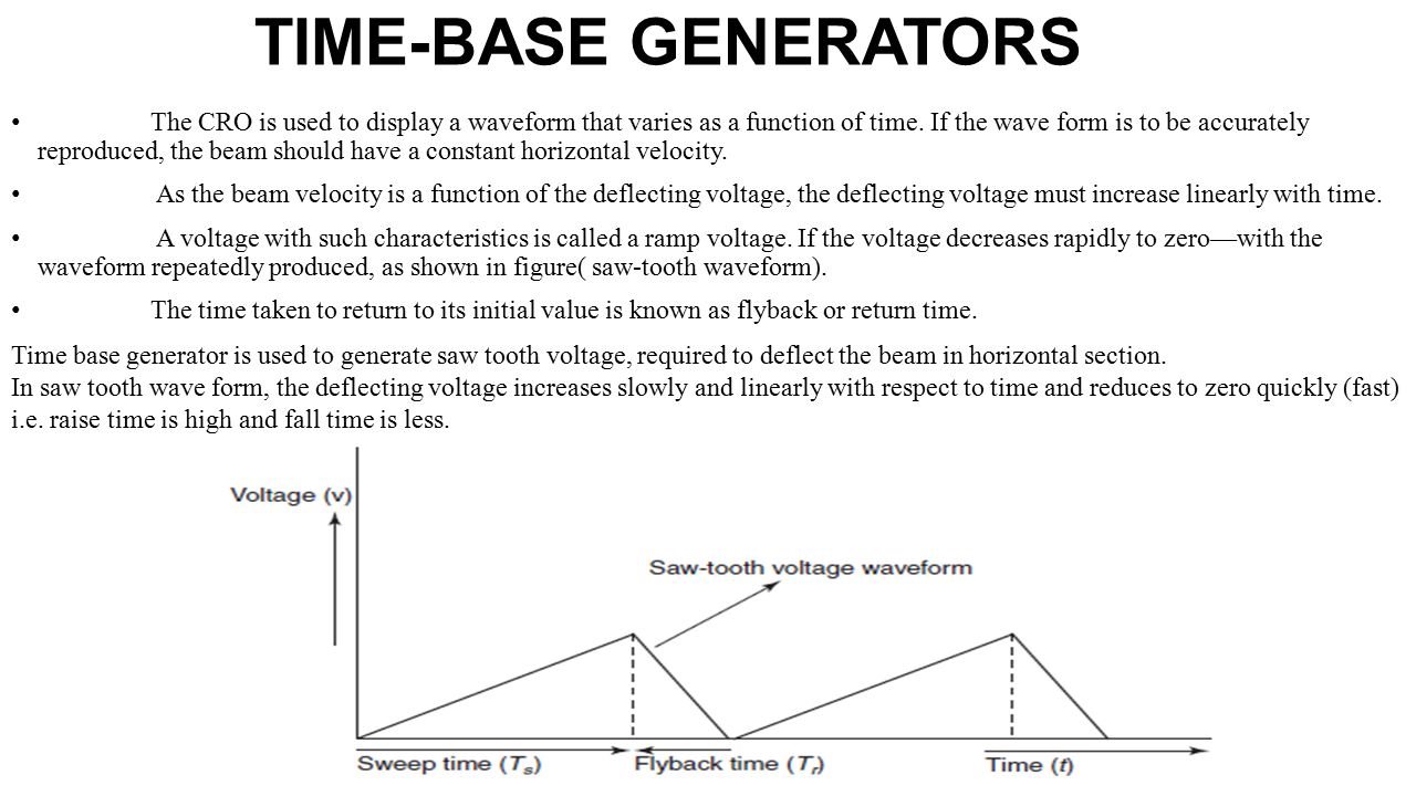
5 . TIME BASE GENERATOR
A time base generators, or timebase, is a special type of function generator, an electronic circuit that generates a varying voltage to produce a particular waveform. Time base generators produce very high frequency sawtooth waves specifically designed to deflect the beam in cathode ray tube (CRT) smoothly across the face of the tube and then return it to its starting position.
Time bases are used by radar systems to determine range to a target, by comparing the current location along the time base to the time of arrival of radio echoes. Analog television systems using CRTs had two time bases, one for deflecting the beam horizontally in a rapid movement, and another pulling it down the screen 60 times per second. Oscilloscopes often have several time bases, but these may be more flexible function generators able to produce many waveforms as well as a simple time base.
Description

A cathode ray tube (CRT) consists of three primary parts, the electron gun that provides a stream of accelerated electrons, the phosphor-covered screen that lights up when the electrons hit it, and the deflection plates that use magnetic or electric fields to deflect the electrons in-flight and allows them to be directed around the screen. It is the ability for the electron stream to be rapidly moved using the deflection plates that allows the CRT to be used to display very rapid signals, like those of a television signal or to be used for radio direction finding (see huff-duff).
Many signals of interest vary over time at a very rapid rate, but have an underlying periodic nature. Radio signals, for instance, have a base frequency, the carrier, which forms the basis for the signal. Sounds are modulated into the carrier by modifying the signal, either in amplitude (AM), frequency (FM) or similar techniques. To display such a signal on an oscilloscope for examination, it is desirable to have the electron beam sweep across the screen so that the electron beam cycles at the same frequency as the carrier, or some multiple of that base frequency.
This is the purpose of the time base generator, which is attached to one of the set of deflection plates, normally the X axis, while the amplified output of the radio signal is sent to the other axis, normally Y. The result is a visual re-creation of the original waveform.
Use in radar
A typical radar system broadcasts a short pulse of radio signal and then listens for echoes from distant objects. As the signal travels at the speed of light and has to travel to the target object and back, the distance to the target can be determined by measuring the delay between the broadcast and reception, 'time base generators, or timebase, is a special type of function generator, an electronic circuit that generates a varying voltage to produce a particular waveform. Time base generators produce very high frequency sawtooth waves specifically designed to deflect the beam in cathode ray tube (CRT) smoothly across the face of the tube and then return it to its starting position.
Time bases are used by radar systems to determine range to a target, by comparing the current location along the time base to the time of arrival of radio echoes. Analog television systems using CRTs had two time bases, one for deflecting the beam horizontally in a rapid movement, and another pulling it down the screen 60 times per second. Oscilloscopes often have several time bases, but these may be more flexible function generators able to produce many waveforms as well as a simple time base.
Description
A cathode ray tube (CRT) consists of three primary parts, the electron gun that provides a stream of accelerated electrons, the phosphor-covered screen that lights up when the electrons hit it, and the deflection plates that use magnetic or electric fields to deflect the electrons in-flight and allows them to be directed around the screen. It is the ability for the electron stream to be rapidly moved using the deflection plates that allows the CRT to be used to display very rapid signals, like those of a television signal or to be used for radio direction finding (see huff-duff).
Many signals of interest vary over time at a very rapid rate, but have an underlying periodic nature. Radio signals, for instance, have a base frequency, the carrier, which forms the basis for the signal. Sounds are modulated into the carrier by modifying the signal, either in amplitude (AM), frequency (FM) or similar techniques. To display such a signal on an oscilloscope for examination, it is desirable to have the electron beam sweep across the screen so that the electron beam cycles at the same frequency as the carrier, or some multiple of that base frequency.
This is the purpose of the time base generator, which is attached to one of the set of deflection plates, normally the X axis, while the amplified output of the radio signal is sent to the other axis, normally Y. The result is a visual re-creation of the original waveform.
Use in radar
A typical radar system broadcasts a short pulse of radio signal and then listens for echoes from distant objects. As the signal travels at the speed of light and has to travel to the target object and back, the distance to the target can be determined by measuring the delay between the broadcast and reception, multipling the speed of light by that time, and then dividing by two (there and back again). As this process occurs very rapidly, a CRT is used to display the signal and look for the echoes.
In the simplest version of a radar display, today known as an "A-scope", a time base generator sweeps the display across the screen so that it reaches one side at the time when the signal has travelled the radar's maximum effective distance. For instance, an early warning radar like Chain Home (CH) might have a maximum range of 150 kilometres (93 mi), a distance that light will travel out and back in 1 millisecond. This would be used with a time base generator that pulls the beam across the CRT once every millisecond, starting the sweep when the broadcast signal ends. Any echoes cause the beam to deflect down (in the case of CH) as it moves across the display.
By measuring the physical location of the "blip" on the CRT, one can determine the range to the target. For instance, if a particular radar has a time base of 1 millisecond, then its maximum range is 150 km. If this is displayed on a four-inch CRT and the blip is measured to be 2 inches from the left side, then the target is 0.5 milliseconds away, or about 75 kilometres (47 mi).
To ensure the blips would line up properly with a mechanical scale, the time base could be adjusted to start its sweep at a certain time. This could be adjusted manually, or automatically trigged by another signal, normally a greatly attenuated version of the broadcast signal.
Later systems modified the time base to include a second signal that periodically produced blips on the display, providing a clock signal that varied with the time base and thus did not need to be aligned. In UK terminology, these were known as strobes.
Use in television
Television signals consist of a series of still images broadcast in sequence, in the NTSC standard such a "frame" is broadcast 30 times a second. Each frame is itself broken down into a series of "lines", 525 in the NTSC standard. If one examines a television broadcast on an oscilloscope, it will appear to be a continual sequence of modulated signals broken up by short periods of "empty" signal. Each modulated portion carries the analog image for a single line.
To display the signal, two time bases are used. One sweeps the beam horizontally from left to right at 15,750 times a second, the time it takes for one line to be sent. A second time base causes the beam to scan down the screen 60 times a second, so that each line appears below the last one drawn and then returns to the top. This causes the entire signal of 525 lines to be drawn down the screen, re-creating a 2-dimensional image.
To ensure the time base began its sweep of the screen at the right time, the signal included several special modulations. With each line there was a brief period, the "front porch" and "back porch" that caused the signal to go negative briefly. This triggered the horizontal time base to start its sweep across the screen, ensuring that the lines started on the left of the display. A much longer but otherwise similar signal, the vertical blanking interval caused the vertical time base to start, with any lengthy delay causing the time base to trigger.
---------------------------------------------------------------------------------------------------------------------------------------------
6 . Time Base Display


------------------------------------------------------------------------------------------------------------------------------------------
7 . TIME TRACK
Inputs


Processing
Hourly processes, analyses and learns based on historical data and future holidays
Outputs


1.Computed predictions for working hours & billables
2. Missing & incomplete times detection and helpful prompts
3. Insightful reports and email summaries
4. Real-time drafts for invoices & time sheets
5. Beautiful web invoices for clients
-------------------------------------------------------------------------------------------------------------------------------------
Gen.Mac Tech in activities aimed at space and time interfaces for the Power saving Timer is reviewed at this time, namely the 20th and 21st centuries.

Pro Life -- Pro Family -- Pro Gun --- Pro Modern Live = POWER SAVING
___ 💗 💗 💗 💗 💗 💗 💗 💗 💗 ______