


The schematics are categorized in clear and self-explained categories in order to help you find what you are looking for fast and easy.
every time you choose to view a document. This is done for several reasons:
- 1. For copyright reasons
- 2. Space economy: Most of the circuits belong to hobbyists that may host up to some tens of circuits or even less. This would require a very small amount of disk space. Our archive has gather some thousands of circuits. This would require a significant amount of disk space.
- 3. PCB Heaven circuits archive is a the librarian, not the library. This means that our intention is to find, categorize and help you discover the circuit you want

Q . I 4511B BCD to 7-segment decoder driver
1. Pin connections
| 4511B pin connections |
How to Build a 4511 BCD to 7 Segment Decoder Circuit
In this circuit, we will build a BCD to 7 segment display decoder circuit using the 4511 chip.
A BCD to 7 segment decoder circuit is a circuit that intakes a binary value and displays the equivalent decimal value on the 7 segment display.
Using binary coded decimal (BCD), we can display any numerical digit on the 7 segment display from 0 to 9- using only 4 pins. Otherwise, without this chip, to display all the decimal digits (0-9), you would have to use 7 pins; so it saves us 3 pins.
How the 4511 BCD to 7 segment display decoder works is it has 4 pins that intake a binary value. Each of these 4 pins can hold a 0 (LOW) or a 1 (HIGH). These data pins are referred to in the datasheet as D, B, C, and A. We can choose what digit we want to display by inputting the equivalent binary value into these data pins. For example, if we want to display 6 on the 7 segment display, we input the value 0110 into the DBCA data pins. The binary value 0110 is the equivalent of the decimal value of 6. This is why it's called binary coded decimal. With the binary value input, the equivalent decimal value of that binary number is displayed on the 7 segment display. Otherwise, you would have to know which pins on the 7 segment display to turn on or off, making it much more complicated. This chip saves us a lot of work for that reason.
In this circuit, we will start the 4511 BCD to 7 segment display decoder with the most basic circuit. We will connect this chip by itself to pushbuttons. Using the pushbuttons, you can manually see how depending on which pushbuttons we press, how the output changes in response. So we can see which combinations of pushbuttons turned on displays which decimal values.
Below, we will also explain how BCD to 7 segment display decoders work in great detail, specifically the 4511 chip.
Components
- 4511 BCD to 7 Segment Display Decoder
- 7 segment display
- 4 1KΩ resistors
- 7 470Ω resistors
- 4 pushbuttons
The 4511 BCD to 7 segment display decoder can be gotten very cheaply for under $1 on ebay.
The 4511 chip takes in a binary value and displays the equivalent decimal value on the 7 segment display.
The 4511 is a 16-pin chip. The pinout of the 4511 is shown below.
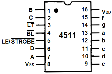
To power the chip, VDD, pin 16 to 5V and VSS, pin 8, connects to ground. The 4511 chip is capable of handling up to 20V.
The 4 input data pins, which control the digit which is shown on the 7-segment LED display, are D, C, B, and A which are pins 6, 2, 1, and 7, respectively. These 4 data pins are fed binary values. Connecting a pin to VCC puts the pin in a HIGH state or value. Connecting a pin to ground or 0V puts the pin in a LOW state or value. This is how we adjust the value of these data pins. There are 4 data pins hold a binary value. The decimal equivalent of the binary value that it holds will be displayed on the 7 segment display. So, for example, if we want to show the decimal number 5, we give a value of 0101 to the DCBA data pins.
Pin 3 is the LT pin, which is the Lamp Test pin. This pin is active LOW. When HIGH, the lamp test is activated. This makes all the outputs HIGH, so if LEDs are attached to all of the outputs, all of the LEDs will turn on if this pin is HIGH. When LOW, this feature is not activated. It's simply to test all the outputs to check if they turn on.
Pin 4 is the Blanking pin. This pin is active LOW. When HIGH, all the outputs go LOW, so they'll all shut off, like a reset pin. When HIGH, this feature is not ativated.
The LE/STROBE pin is the Latch Enable/STROBE has dual purposes depending on whether it's HIGH or LOW. When LOW, the pin is in strobe mode, meaning it strobes the output to a given device, which in this case is a 7 segment LED display. This mode is the mode we usually want it in for display purposes. So in normal operation, it's held LOW. When HIGH, it is store mode. So it simply stores latches or stores the data without transferring to a device.
Lastly, the 8 output pins are labeled a, b, c, d, e, f g, which are pins 12, 12, 11, 10, 9, 15, and 14. These are the pins we attach to each of the corresponding pins on the 7 segment LED display. For example, a on the 4511 matches to a on the 7 segment LED display, b matches with b, etc.
The decimal digit that the 7 segment display shows out depends on the binary value fed into the 4 input data pins DBCA.
The table below summarizes the binary input values to the decimal digit shown on the 7 segment display.
| Binary Coded Decimal Chart | |||||
| Decimal Number | Binary Word | B8 | B4 | B2 | B1 |
| 0 | 0000 | Low | Low | Low | Low |
| 1 | 0001 | Low | Low | Low | High |
| 2 | 0010 | Low | Low | High | Low |
| 3 | 0011 | Low | Low | High | High |
| 4 | 0100 | Low | High | Low | Low |
| 5 | 0101 | Low | High | Low | High |
| 6 | 0110 | Low | High | High | Low |
| 7 | 0111 | Low | High | High | High |
| 8 | 1000 | High | Low | Low | Low |
| 9 | 1001 | High | Low | Low | High |
You can see based on this chart why it's a binary coded decimal system.
If we input a binary value into the data pins, we get the corresponding decimal digit equivalent shown out on the 7 segment display.
So, for example, if we input 0000 into the data pins, we get the number 0.
4511 BCD to 7 Segment Display Decoder Circuit
The 4511 BCD to 7 segment display decoder circuit we will build is shown below.
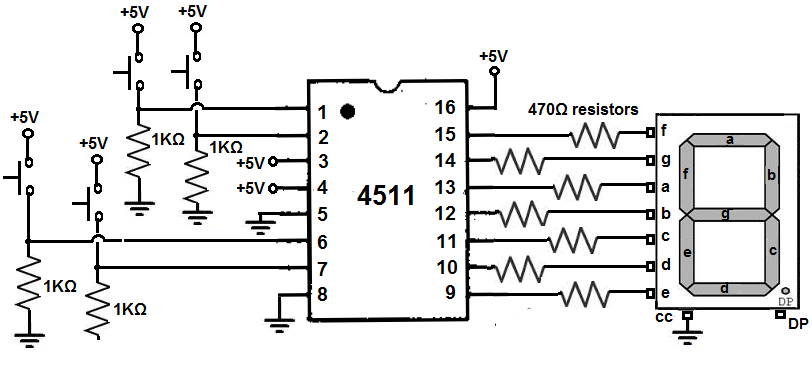
First, to power the 4511 chip, we connect VDD, pin 16, to +5V and VSS, pin 8, to ground. This establishes sufficient power to the 4511 chip.
The LT pin, pin 3, is connected to +5V. This pin would turn on all the outputs if connected LOW. Being that we don't wish to use this feature, we simply connect it permanently HIGH. However, if you do want to use this feature, you can simply connect it to a pull-up resistor with a pushbutton. When unpressed, the pin will be HIGH. When pressed down, it would be LOW and turn on all the outputs.
The Blanking pin, pin 4, is connected to +5V. This pin would blank all the outputs if connected LOW or to ground. Being that we don't want the blanking feature activated, we simply connect it permanently to HIGH. However, if you want to use this feature in your circuit, you simply connect a pull-up resistor to this pin with a pushbutton. When unpressed, the pin will be HIGH. When pressed, it will go LOW and turn off all the outputs.
The LE/STROBE pin, pin 5, is connected to ground. This is because we want to strobe the outputs to the 7 segment LED display.
The 4 data pins are D, B, C, and A. These pins are all connected to pull-down resistors. Without the pushbuttons being pressed, the pins are all in a LOW state. If the pushbuttons are pressed, they go to a HIGH state. Depending on the combination of pushbuttons being pressed determines the decimal digit that will be shown on the 7 segment LED display; this is summarized in the table above.
To each of the output pins, a through g, we connect an LED with a 470Ω current-limiting resistor.
How the Circuit Works
The circuit works directly through the control of the 4 pushbuttons which control the binary value we feed into the data input pins.
Being that they are all connected to pull-down resistors, they are all initially LOW when unpressed. So the 7 segment LED display will show a 0 initially.
The combination of pushbuttons pressed and unpressed determines the decimal digits, according to the binary value. The equivalent decimal value of the binary value we feed into the data input pins will be shown.
We can show the digits 0 through 9. We cannot show any other digits on the 7 segment display. So the highest value we can feed into is 1001, which is 9 in decimal. Any value above this amount cannot be shown on the 7 segment LED display.
So if we want to show a 4, we pressed down on pushbutton C while having all the other pushbuttons unpressed. You should now see a 4 on the 7 segment LED display.
The 4511 really makes it much simpler to work with single 7 segment LED displays.
To see how to make a 7 segment display count up from 0 to 9 or count down from 9 to 0 automatically without any manual pushbutton intervention, we can connect a binary up/down counter to this circuit. 7 Segment LED Counter This simple counter can be used to count pulses, as the basis for a customer counter (like you see at the doors of some stores), or for anything else that may be counted. The circuit accepts any TTL compatible logic signal, and can be expanded easily (see Notes).
Interfacing to 7-Segment Numeric Displays

7-Segment Numeric LED Displays
In industrial PLC applications, one of the old, but simpler methods of displaying numeric information is to use one or more 7-Segment numeric displays connected to an output card of a PLC... Although it is possible to build such a display yourself, it is far more common to employ a pre-manufactured product such as the 4-digit panel mount unit shown at the top of this page...
To correctly interface a PLC to such a display, it helps to first understand what basic electronic components are typically employed in their makeup, and how this effects our task of interfacing to, and programming such a unit... Although both LED and LCD numeric displays are readily available, and interfaced similarly, we'll concentrate on the more common LED units in the examples to follow...


BCD to 7-Segment Decoder c/w 4-bit Latch
Once 7-Segment LED displays became readily available, a simple IC known as a "BCD to 7-Segment decoder" was quickly developed to simplify their use... Binary formatted data presented to this IC's inputs results in the IC's outputs being placed into the correct state to display the equivalent numeral (0 to 9) on a 7-Segment display...
Although BCD to 7-Segment decoder ICs are available without built in latches, this particular IC includes a built in 4-bit latch which we will make use of in later examples... For now the latch is set to simply allow input data to freely pass through to the decoder...

In the above diagram, the 4 toggle switches, SW0 to SW3 are used to select the desired numeral (0-9) that will appear on the 7-Segment display... By using a decoder, it's now simply a matter of setting the correct 4-bit BCD pattern feeding the inputs of the decoder, and the decoder takes care of the rest...
The decoder section also has two additional inputs... Lamp Test (LT) turns all segments on so you can verify at once that all display segments are working, or identify display units that need to be replaced... This input is normally left at logic 1... The Blanking (BL) input is just the reverse; it forces the entire display off... This is used in many cases to blank out leading or trailing zeros from a long display... LT will override BL so you can test even blanked-out display digits...
One should also note that the same circuit could conceivably be controlled by a PLC, if 4 output bits from a 5VDC PLC output card were used in place of the 4 switches shown... If an 8-bit output card were available, then two such circuits (2 digits) could be controlled... A 16-bit card would in turn allow us to control four such circuits (4 digits)..etc...
Parallel Non-Multiplexed Multiple Digit Display


The figure (above) on the left is taken from the LogixPro I/O simulator screen, and depicts a common method of interfacing to a 4 digit display... The figures on the right are taken from the data sheet of a pre-manufactured 4 digit display unit which could be readily employed in this particular application...
The manufactured unit does contain four separate circuits, and each circuit (digit) has it's own decoder, but compared to our earlier circuit example, this unit employs additional components and circuitry making it far more versatile and easy to use...
Note that there are 4 "Strobe" lines shown; one for each digit... These strobe lines control built in IC latches which provide us with the option of multiplexing the digits, or displays, if we wished to do so... In the above non-multiplexed application, the strobes are permanently enabled allowing data to simply pass through from the BCD inputs and be displayed as normal...
Also note that this particular unit is designed for 24VDC use... This is by far the most common DC voltage level used in industrial installations, and PLC I/O cards designed for such use are therefore extremely common... In comparison to 5VDC circuits, 24VDC circuits can typically tolerate far greater supply voltage excursions, are less sensitive to the effects of contact resistance, and more tolerant of electrically noisy environments...
Multiplexed Digits
By making use of the 4-bit latches that are built into the 4511 IC, we can easily multiplex the digits if so desired... By properly controlling the state of each latch enable pin (LE) we can use the same input data lines (4 switches) to selectively write to each 7-Segment display independently... With just a minor modification to our circuit, we will be able to essentially treat each digit as a unique 4-bit memory location where BCD data of our choosing can be stored and retained...

In the above schematic diagram, each display may be written to separately... First the BCD equivalent of the desired numeral (0-9) is set using the 4 data switches... If SW1 is then closed, the current BCD input data will enter the latch of the upper 4511 IC, and will be passed on to the decoder causing the numeral to displayed... if SW1 is then opened, the latch will retain the current data, but will now ignore any changes on it's inputs... The desired numeral will continue to be displayed by the upper LED display until power is lost, or SW1 is again closed and new data is allowed to enter it's latch...
The Lower 7-Segment display may be written to in a similar fashion... Set the BCD equivalent of the desired digit using the 4 data switches, then close SW2 momentarily to store and retain the current BCD data... We might say that we are strobing the data into the display...
We could readily replace the 4 data switches and 2 latch switches if we had 6 5VDC outputs available on our PLC... If we wished to add additional digits, we would require 1 more PLC output for each digit added... By multiplexing the data in this fashion we would only require 8 PLC outputs to control a 4 digit display...
4 Digit Display configured for Multiplexed Digits

By using multiplexed data lines as shown above, we can dramatically reduce the number of PLC outputs required (8) to control this 4 digit display... The down side is that writing a ladder logic program to update a display wired in this fashion will be somewhat more complicated then one written to control 4 digits wired in parallel...
If you have been looking closely, you may have questioned the purpose of the dual inline sockets located on the wiring PCB of this manufactured display unit.. Well essentially the 16 data lines are internally connected in parallel with these sockets, and this allows us to easily add additional units by simply interconnecting them using a flat ribbon cable assembly...
Multiple 4 Digit Displays configured for Multiplexed Digits

For those with a fundamental knowledge of computers, you'll likely note that we have essentially created a 4-bit data bus, and the strobe lines are in effect our address bus... We can continue to add additional digits, and for each digit added we will require 1 additional PLC output, or 4 outputs per quad display...1 Quad Display requires 4 data + 4 strobes = 8 outputs
2 Quad Displays requires 4 data + 8 strobes = 12 outputs
3 Quad Displays requires 4 data + 12 strobes = 16 outputs
4 Quad Displays requires 4 data + 16 strobes = 20 outputs
If you are reading through this tutorial because you are having difficulty determining how to control the 4 quad displays in the Bottle Line Simulation, you may already have noted that the displays in that simulation do not employ muxed (multiplexed) digits, but rather the quad displays themselves are muxed... Why this method was chosen, will be investigated now...
Multiplexed 4 Digit Displays ..... (Bottle Line Simulation)

The above diagram functionally depicts how the 4 panel mounted display units in the Bottle Line simulation are deemed to be configured... In this case, the 4 manufactured displays are wired to a shared 16-bit data bus (wires) which is connected to a 16-bit 24VDC output card (O:4) that is dedicated to this purpose... 4 unused outputs from card O:2 were selected, and appropriately wired to allow control of the strobe lines associated with each display unit...
Each unit may be written to individually by first sending the 16 bit BCD representation of the 4 decimal numerals to output card O:2... If one of the four output bits 0:2/11 to O:2/14 is then taken from an initial low, to high state, the BCD data will enter the selected latches, and the numerals will be displayed... If this strobe line is then returned to the initial low state, the BCD data will (be latched) remain in the latches, and continue to be displayed... Any changes in the state of the data lines will now be ignored, and this will continue until the next low-to-high transition of this unit's strobe line occurs...
You may have noted that this configuration requires a high level on the strobe line to allow data to enter the latch, while some of our earlier examples required a low state... The polarity of the strobe is non critical, and with this particular make of display, the choice of polarity is set by simply positioning a configuration DIP switch appropriately...
Multiplexed Digits vs Displays
There are no hard and fast rules relating to this issue, but a quick look at the following chart does provide some food for thought...
................................Muxed Digits....Muxed Displays
1 Quad Display requires.......8 outputs......16 outputs (no muxing)
2 Quad Displays requires.....12 outputs......18 outputs
3 Quad Displays requires.....16 outputs......19 outputs
4 Quad Displays requires.....20 outputs......20 outputs
5 Quad Displays requires.....24 outputs......21 outputs
6 Quad Displays requires.....28 outputs......22 outputs
10 Quad Displays requires....44 outputs......26 outputs
Another consideration relates to ease of programming... The task of writing digits one at a time is obviously going to be a greater challenge then writing 4 digits at a time... Also, fewer instructions typically equates to an easier to read program, plus a quicker scan... If you need to control 4 quad displays, muxed displays would be my choice... Need 10 displays, and it might be time to consider some other means of presenting information to the operator... Human machine interface
micro engineer
some way to get input to the microcontroller and some way to display information from the micro. Let's start taking a look at I/O, with the concentration this time on the O.
Sometimes you just need to be able to light up an indicator to give you an idea of what is happening - power on. At other times it would be nice to display several numbers, or even words. We'll start with a simple light, move up to numbers, and maybe next time, words.
The most common indicator these days is the light emitting diode, or LED. Just a few years ago, they didn't exist. Now they are in everything, because of their low cost, long life, low current requirements and overall colorful personality.
LEDs come in red, orange, yellow, green and even blue is becoming reasonably priced. In general, they require around 2 volts to operate, though some have built-in regulators to run from 5 volts and some even have flasher circuits built-in. You can get a single LED for an indicator light, or you can buy several all packaged up in a matrix of dots or numeric segments.
Since LEDs run on about 2 volts, you can't shove 5 volts through them and expect them to take it like a man. You need a simple resistor in series to absorb some of the voltage and limit the current the LED can draw. You should check the specifications for your particular LED to calculate the exact resistor value. Of course, you can rarely find the specs on the generic LED you just got from your parts house, so we'll just use generic specs: 2 volts at 10 milliamps (ma) of current. You can choose more or less current depending on how bright you want the LED (up to a point) and how efficient your LED is (some light up with just 1ma of current.)
So if we start with 5 volts and the LED drops 2 volts, our series resistor needs to drop the remaining 3 volts. Using the old V = IR equation (no, it isn't just for infrared LEDs), V is 3 volts, I is 10ma (.010 amps), we can solve for R: R = V/I = 3/.010 = 300 ohms. That didn't hurt too much did it?
Of course, finding a 300 ohm resistor could be a pain. The more common ones have odd, non-decimal values. The closest ones for us are 270 ohms and 330 ohms. I'm going to choose 270 ohms which will increase our current a little, making the LED slightly brighter. Rearranging our equation once more: I = V/R = 3/270 = .0111 amps or 11ma.
The last little gotcha is that LEDs are one-way, one side is plus, the anode, and the other is minus, the cathode. If you hook it up backwards, you can damage the LED, but usually it just won't light up. Most LEDs have one lead longer than the other, the longer one being the plus side (anode.) If you have cut off the legs before checking, you may find that the plastic case is flat towards the minus lead (cathode.)
After all of this, we can finally hook up our power LED as shown:
 As you can see from Figure 1, it doesn't really matter which side of the LED the series resistor is connected to. I know this may be way too basic for some readers, but judging from the phone calls I get, this all needs to be said. Besides, we'll get in over everybody's head by the end of this article.
So far we have an LED that lights up any time power is applied, but how do we control it? We have a choice of connecting one end to ground and turning on and off 5 volts from an I/O pin, or we can connect that end to 5 volts and turn on and off ground. Depending on the application, one way or the other might be appropriate. In many cases, I/O pins can sink more current than they can source. In other words, the drivers that put out ground are more powerful than the drivers that put out 5 volts. So it might be better to connect the LED directly to 5 volts and turn on and off ground to the other end. This confuses some people, so feel free to connect one end to ground and turn on and off 5 volts from the I/O pin. One final consideration is to be sure that the I/O pin of the microcontroller you are using can actually sink or source the necessary 11ma of current. In the case of a PIC®, we can drive well beyond that puny amount.
 Now let's hook up 2 LEDs. It should be about as simple as one and besides, we only need one current limit resistor right? Well, not exactly. Take a look at Figure 3. In the drawing on the left, you can see 2 LEDs connected to 2 I/O lines with 2 series resistors. This is usually what you want to do. Consider the drawing on the right. It should do the same thing with only one current limit resistor - you just saved .005 cents. And if you only turn on one LED at a time, it actually will work fine.
 But look what happens when you turn on both LEDs at the same time. The resistor will still follow Ohm's law as described above, drop 3 volts and limit the current to 11ma. However, now that current has to be shared by 2 LEDs. If you are lucky, each LED will get 5.5ma. But it is more likely that the split will be uneven and one will draw more current than the other. In either case, the LEDs will be quite a bit dimmer than if each had its own allotment of 11ma.
The normal end to this story would be: use 2 resistors. But we have a microcontroller on duty. Perhaps the biggest benefit of a microcontroller is its ability to trade hardware for software. Maybe you just don't have the extra .005 cents for the resistor, not to mention the assembly cost and board space required for it. Remember we said earlier that as long as we don't turn on both LEDs at the same time, things will work out fine with only one resistor. What we can do with a microcontroller is time-multiplex the LEDs so that only one LED is on at a time. By rapidly turning on and off each LED in sequence, it will appear as if both are on at the same time. It has something to do with the way our eyeballs and brains work, persistence of vision. It is similar to the way that TV works, we can see a steady picture even though there is nothing good on.
Next let's step up to 7 LEDs. And let's arrange them in the shape of a figure 8 like this:
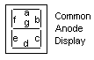
 Wow, with this kind of configuration we can build the numbers 0 - 9 and even some letters. I should patent this idea. Anyway, a 7 segment display consists of 7 individual LEDs with one end of each LED connected together. If all of the plus ends are connected together, it is called common anode. If all of the minuses are connected together, it is called common cathode.
Whether you choose common anode or common cathode depends on how you want to hook things up. I am going to choose common anode with all the pluses connected together for reasons you will see shortly. Figure 5 shows one way to connect the display to a PIC. The 8 cathode lines are connected to the 8 PortB lines through series resistors. 8? What happened to 7 segments? I have also connected the decimal point for good measure. The common anode line is connected to 5 volts.
 We could use the technique described above and put only one current limit resistor in the common line to 5 volts. However we would have to light up each segment one at a time over and over again in order to display a complete character. We would need to do this at least 100 times per second (1000 times per second is better) to cut down flicker. If you only have one 7 segment display in your project, this could be workable. But we are going to add more.
To add another display, we could use 8 more I/O lines, connecting the next display to PortC, for example. While it makes programming easier, it eats up I/O pins in a hurry. You could also add separate latches or even decoders for each display, but, once again, we are going to use software instead of hardware.
 As you can see in Figure 6, the cathodes from a particular segment of each display are all connected together and then connected to a PIC I/O line through a series resistor. We have also removed each common anode from 5 volts and made it controllable by a PIC I/O pin. In this manner, we can set up the segment value for a given display and then briefly turn on the anode for that display. If we do each one fast enough, we will see the entire display, flicker free.
Remember earlier we chose common anode? Let's take a look at current considerations to see why. The PIC is now driving up to 8 LEDs (segments) at a time off a single port. Just as each I/O pin has a limit to the amount of current it will source or sink, each port also has a limit. To do the least damage, we are sinking the current to ground rather than sourcing it to 5 volts.
You'll also note in the figure that I snuck in a transistor between the PIC and the common anode to each display. Since the current for the entire display runs through this one pin, it could overload a single I/O line. The transistor amplifies the current drive capability of the I/O line to solve this dilemma. It is easy to operate, put ground on the I/O pin to turn on the transistor and enable a given display, put 5 volts on the pin to turn off the transistor and the display.
Now all we need is software. The first task is to figure out how to get numbers (and even some letters) on the display. All we really have right now are a bunch of individual LEDs connected to I/O pins. To form characters, we need to come up with a way to turn on specific ones while leaving others off.
Let's look at the case of 8. Eight is pretty simple. It is all the LEDs (except the decimal point) on. To display 8 we need to put a binary 1000 0000 on PortB. This will turn on all the LEDs except the decimal point. 0 = on? Remember, we are controlling the minus side of the LEDs. We also need to put a value onto PortA to address a specific LED digit, 1110. Once again, 0 will turn on one of the transistors and 1 will ensure the others are off.
The number 0 is simply an 8 with the middle segment off, 1100 0000. Now we could have a subroutine to decode each digit, but that gets long and I hate to type (hard to tell?) The easiest way to proceed is by using a lookup table. This method is particularly effective when you have a limited number of combinations of desired states, in our case 10 (0-9.)
Now by simply using the number we wish to display, 0 - 9, as the index into the lookup table, we can easily find the proper value to put onto the I/O port. You can even extend the lookup table to include some letters, a - f perhaps.
In Microchip assembler, the code looks something like this:
The jump table feature of PICs is pretty amusing. There is actually no other way to get constant data into a program, other than moving literals, of course. The jump works like this: You load W with the index to the particular item you want out of the table. You then call the jump routine. There is one instruction at the top of your jump table. It says to add W to the current program counter. This effects the jump right to your item. The item itself is a line that says return the constant value you want in W, right back to the caller. It is pretty quick and simple, once you get the hang of it. The one gotcha here is that the table must be all in one page. You also need to preset PCLATH if it is not in the page you are in.
In PICBASIC, the display routine looks something like this:
This gets you the basic format to light up a single digit. All that remains is to write the code that separates a binary number into the 4 decimal digits and display each digit. It's kind of a pain to write in assembler, so here's some more PICBASIC code:
Don't forget you want to call this routine continuously, or at least as often as possible, to reduce the amount of flicker. Of course, this is the biggest drawback with using LEDs: You have to continuously scan the data out to the displays.
Another American company called Motorola, quickly realized what was going on, so they launched 8-bit microprocessor 6800. Their chief constructor was Chuck Peddle. Apart from the processor itself, Motorola was the first company that also manufactured other peripherals such as the 6820 and 6850. At that time many companies recognized the greater importance of microprocessors and began their own development. Chuck Peddle left Motorola to join MOS Technology and kept working intensively on developing microprocessors.
At the WESCON exhibition in the USA in 1975, a crucial event in the history of the microprocessors took place. MOS Technology announced that it was selling processors 6501 and 6502 at $25 each, that interested customers could purchase immediately. It was such a sensation that many thought it was a kind of fraud, considering that competing companies were selling the 8080 and 6800 at $179 each. On the first day of the exhibit, in response to the competitor, both Motorola and Intel cut the prices of their microprocessors to $69.95. Motorola accused MOS Technology and Chuck Peddle of plagiarizing the protected 6800. Because of that, MOS Technology gave up further manufacture of the 6501, but kept manufacturing the 6502. It was the 8-bit microprocessor with 56 instructions and ability to directly address 64Kb of memory. Due to low price, 6502 became very popular so it was installed into computers such as KIM-1, Apple I, Apple II, Atari, Commodore, Acorn, Oric, Galeb, Orao, Ultra and many others. Soon several companies began manufacturing the 6502 (Rockwell, Sznertek, GTE, NCR, Ricoh, Commodore took over MOS Technology). In the year of its prosperity 1982, this processor was being sold at a rate of 15 million processors per year!
Other companies did not want to give up either. Frederico Faggin left Intel and started his own company Zilog Inc. In 1976 Zilog announced the Z80. When designing this microprocessor Faggin made a crucial decision. The 8080 had already been developed and he realized that many would remain loyal to that processor because of the great expenditures which rewriting of all the programs would result in. Accordingly he decided that a new processor had to be compatible with the 8080, i.e. it had to be able to perform all the programs written for the 8080. Apart from that, many other features have been added so that the Z80 was the most powerful microprocessor at that time. It was able to directly address 64Kb of memory, had 176 instructions, a large number of registers, a built-in option for refreshing dynamic RAM memory, a single power supply, greater operating speed etc. The Z80 was a great success and everybody replaced the 8080 by the Z80. Certainly the Z80 was commercially the most successful 8-bit microprocessor at that time. Besides Zilog, other new manufacturers such as Mostek, NEC, SHARP and SGS appeared soon. The Z80 was the heart of many computers such as: Spectrum, Partner, TRS703, Z-3 and Galaxy.
In 1976 Intel came up with an upgraded version of the 8-bit microprocessor called the 8085. However, the Z80 was so much better that Intel lost the battle. Even though a few more microprocessors appeared later on the market (6809, 2650, SC/MP etc.), the die had already been cast. There were no such great improvements which could make manufacturers to change their mind, so the 6502 and Z80 along with the 6800 remained chief representatives of the 8-bit microprocessors of that time.
Simply, In order to communicate with peripheral environment, the microprocessor must use specialized circuits added as external chips. In short microprocessors are the pure heart of the computers. This is how it was in the beginning and remains the same today.


Excepting strictly controlled laboratory conditions, the most complicated electronic circuits cannot accurately determine the difference between two sizes (two voltage values, for example) if they are too small (lower than several volts). The reasons are electrical noises and something called the “real working environment” (unpredictable changes of power supply voltage, temperature changes, tolerance to values of built in components etc.). Imagine a computer which would operate upon decimal numbers by recognizing 10 digits in the following way: 0=0V, 1=5V, 2=10V, 3=15V, 4=20V… 9=45V !? Did anybody say batteries? A far simpler solution is the use of binary logic where 0 indicates that there is no voltage and 1 indicates that there is voltage. It is easier to write 0 or 1 instead of “there is no voltage” or “there is voltage”. It is called logic zero (0) and logic one (1) which electronics perfectly conforms with and easily performs all those endlessly complex mathematical operations. It is electronics which in reality applies mathematics in which all numbers are represented by two digits only and in which it is only important to know whether there is voltage or not. Of course, we are talking about digital electronics.

110 = 1*2^2 + 1*2^1 + 0*2^0 = 6
It should be noted that for decimal numbers from 0 to 3 you only need two binary digits. For greater values, extra binary digits must be added. Thus, for numbers from 0 to 7 you need three digits, for numbers from 0 to 15- four digits etc. Simply speaking, the largest binary number consisting of n digits is obtained when the base 2 is raised by n. The result should be then subtracted by 1. For example, if n=4:
2^4 – 1 = 16 – 1 = 15
Accordingly, using 4 binary digits it is possible to represent decimal numbers from 0 to 15, including these two digits, which amounts to 16 different values in total.


Don’t be confused if you find some bit has value 4, 16 or 64. It means that bit’s values are represented in decimal system. Simply, we have got so much accustomed to the usage of decimal numbers that these expressions became common. It would be correct to say for example, “the value of sixth bit in binary number is equivalent to decimal number 64”. But we are human and habits die hard… Besides, how would it sound “number: one-onezero- one-zero…”
A nibble is referred to as half a byte. Depending on which half of the byte we are talking about (left or right), there are “high” and “low” nibbles.

The operation of these elements is based on the principles established by British mathematician George Boole in the middle of the 19th century- even before the first bulb was invented! In brief, the main idea was to express logical forms through algebraic functions. Such thinking was soon transformed into a practical product which far later evaluated in what today is known as AND, OR and NOT logic circuits. The principle of their operation is known as Boolean algebra. As some program instructions used by the microcontroller perform the same way as logic gates except in the form of commands, the principle of their operation will be discussed here.


Another important pin function is that it can have pull-up resistors. These resistors connect pins to the positive power supply voltage and their effect is visible when the pin is configured as an input connected to mechanical switch or push button. Newer versions of microcontrollers have pull-up resistors configurable by software.
Usually, each I/O port is under control of another SFR, which means that each bit of that register determines the state of the corresponding microcontroller pin. For example, by writing logic one (1) to one bit of that control register SFR, the appropriate port pin is automatically configured as input. It means that voltage brought to that pin can be read as logic 0 or 1. Otherwise, by writing zero to the SFR, the appropriate port pin is configured as an output. Its voltage (0V or 5V) corresponds to the state of the appropriate bit of the port register.

Masked ROM. Microcontrollers containing this ROM are reserved for the great manufacturers. Program is loaded into the chip by the manufacturer. In case of large scale manufacture, the price is very low. Forget it…
One Time Programmable ROM (OTP ROM). If the microcontroller contains this memory, you can download a program into this memory, but the process of program downloading is a “one-way ticket”, meaning that it can be done only once. If an error is detected after downloading, the only thing you can do is to download the corrected program to another chip.
 Flash memory. This type of memory was invented in the 80s in the laboratories of INTEL and were represented as the successor to the UV EPROM. Since the contents of this memory can be written and cleared practically an unlimited number of times, the microcontrollers with Flash ROM are ideal for learning, experimentation and small-scale manufacture. Because of its popularity, the most microcontrollers are manufactured in flash versions today. So, if you are going to buy a microcontroller, the type to look for is definitely Flash!
Random Access Memory (RAM)
Once the power supply is off the contents of RAM (Random Access Memory) is cleared. It is used for temporary storing data and intermediate results created and used during the operation of the microcontroller. For example, if the program performs an addition (of whatever), it is necessary to have a register representing what in everyday life is called the “sum”. For that purpose, one of the registers in RAM is called the “sum” and used for storing results of addition.
Electrically Erasable Programmable ROM (EEPROM)
The contents of the EEPROM may be changed during operation (similar to RAM), but remains permanently saved even upon the power supply goes off (similar to ROM). Accordingly, an EEPROM is often used to store values, created during operation, which must be permanently saved. For example, if you design an electronic lock or an alarm, it would be great to enable the user to create and enter a password, but useless if it is lost every time the power supply goes off. The ideal solution is the microcontroller with an embedded EEPROM.
The microcontroller has learnt during its evolution a trick. Instead of checking each pin or bit constantly, the microcontroller delegates the “wait issue” to the “specialist” which will react only when something attention worthy happens.
The signal which informs the central processor about such an event is called an INTERRUPT.

Today, most microcontrollers have built in several different systems for serial communication as a standard equipment. Which of these systems will be used depends on many factors of which the most important are:

It should be noted that it refers to bits, not bytes! It is usually required by the protocol that each byte is transferred along with several control bits. It means that one byte in serial data stream may consist of 11 bits. For example, if the baud rate is 300 bps then maximum 37 and minimum 27 bytes may be transferred per second, which depends on type of connection and protocol in use.
The most commonly used serial communication systems are:

 UART (Universal Asynchronous Receiver/Transmitter)
This connection is asynchronous, which means that a special line for clock signal transmission is not used. In some situations this feature is crucial (for example, radio connection or infrared waves remote control). Since only one communication line is used, both receiver and transmitter operate at the same predefined rate in order to maintain necessary synchronization. This is a very simple way of transferring data since it basically represents conversion of 8-bit data from parallel to serial format. Baud rate is not high up to 1 Mbit/sec.

Brown-out is a potentially dangerous state which occurs at the moment the microcontroller is being turned off or in situations when power supply voltage drops to the limit due to electric noise. As the microcontroller consists of several circuits which have different operating voltage levels, this state can cause its out-of-control performance. In order to prevent it, the microcontroller usually has built-in circuit for brown out reset. This circuit immediately resets the whole electronics when the voltage level drops below the limit.
Reset pin is usually marked as MCLR (Master Clear Reset) and serves for external reset of the microcontroller by applying logic zero (0) or one (1), depending on type of the microcontroller. In case the brown out circuit is not built in, a simple external circuit for brown out reset can be connected to this pin.

Most programs use these miniature electronic “stopwatches”. These are commonly 8- or 16-bit SFRs and their content is automatically incremented by each coming pulse. Once a register is completely loaded – an interrupt is generated!
If the timer registers use an internal quartz oscillator for their operation then it is possible to measure time between two events (if the register value is T1 at the moment measurement has started, and T2 at the moment it has finished, then the elapsed time is equal to the result of subtraction T2-T1). If the registers use pulses coming from external source then such a timer is turned into a counter.
This is only a simple explanation of the operation itself.

One prescaler is usually shared by timer and watch-dog timer, which means that it cannot be used by both of them simultaneously.


If the watchdog timer is enabled, every time it counts up to the program end, the microcontroller reset occurs and program execution starts from the first instruction. The point is to prevent this from happening by using a specific command. The whole idea is based on the fact that every program is executed in several longer or shorter loops.
If instructions which reset the watchdog timer are set at the appropriate program locations, besides commands being regularly executed, then the operation of the watchdog timer will not affect program execution. If for any reason (usually electrical noises in industry), the program counter “gets stuck” on some memory location from which there is no return, the watchdog will not be cleared and the register’s value being constantly incremented will reach the maximum et voila! Reset occurs!


Briefly, they are two different ways of data exchange between CPU and memory.
von-Neumann Architecture

Harvard Architecture
 The advantages of such design are the following:
 RISC (Reduced Instruction Set Computer)
In this case, the microcontroller recognizes and executes only basic operations (addition, subtraction, copying etc.). All other more complicated operations are performed by combining these (for example, multiplication is performed by performing successive addition). The constrains are obvious (try by using only a few words, to explain to someone how to reach the airport in some other city). However, there are also some great advantages. First of all, this language is easy to learn. Besides, the microcontroller is very fast so that it is not possible to see all the arithmetic “acrobatics” it performs. The user can only see the final result of all those operations. At last, it is not so difficult to explain where the airport is if you use the right words. For example: left, right, kilometers etc.
CISC (Complex Instruction Set Computer)
CISC is the opposite of RISC! Microcontrollers designed to recognize more than 200 different instructions can do much and are very fast. However, one needs to understand how to take all that such a rich language offers, which is not at all easy…
Before you start designing some device based on the microcontroller, think of the following: how many input/output lines will I need for operation? Should it perform some other operations than to simply turn relays on/off? Does it need some specialized module such as serial communication, A/D converter etc. When you create a clear picture of what you need, the selection range is considerably reduced, then it is time to think of price. Is your plan to have several same devices? Several hundred? A million? Anyway, you get the point…
If you think of all these things for the very first time then everything seems a bit confusing. For that reason, go step by step. First of all, select the manufacturer, i.e. the family of the microcontrollers you can easily obtain. After that, study one particular model. Learn as much as you need, do not go into details. Solve a specific problem and something incredible will happen- you will be able to handle any model belonging to that family.
Remember learning to ride a bicycle: after several unavoidable bruises at the beginning, you will manage to keep balance and will be able to easily ride any other bicycle. And of course, you will never forget the skill in programming just as you will never forget riding bicycles!
The real name of this microcontroller is PICmicro (Peripheral Interface Controller), but it is better known as PIC. Its first ancestor was designed in 1975 by General Instruments. This chip called PIC1650 was meant for totally different purposes. About ten years later, by adding EEPROM memory, this circuit was transformed into a real PIC microcontroller. Nowadays, Microchip Technology announces a manufacturing of the 5 billionth sample…
In order that you can better understand the reasons for its popularity, we will briefly describe several important things.
All PIC microcontrollers use harvard architecture, which means that their program memory is connected to CPU via more than 8 lines. Depending on the bus width, there are 12-, 14- and 16-bit microcontrollers. The table above shows the main features of these three categories.
As seen in the table on the previous page, excepting “16-bit monsters”- PIC 24FXXX and PIC 24HXXX- all PIC microcontrollers have 8-bit harvard architecture and belong to one out of three large groups. Therefore, depending on the size of a program word there are first, second and third category, i.e. 12-, 14- or 16-bit microcontrollers. Having similar 8- bit core, all of them use the same instruction set and the basic hardware ‘skeleton’ connected to more or less peripheral units.
In order to avoid tedious explanations and endless story about the useful features of different microcontrollers, this book describes the operation of one particular model belonging to “high middle class”. It is about PIC16F887- powerful enough to be worth attention and simple enough to be easily presented to everybody.
Q . II A / D

This 555 timer based circuit is a kind of voltmeter, also an analog to digital converter, that converts the analog input voltage to digital output pulses. The output pulse width is proportional to the difference between the analog input voltage and the voltage across the 4.7 uF capacitor namely 2.5V. It can measure from +5V to +18V
The accuracy is high in the range of 6V to 18V. The readings are about the same with the 10 bit ADC readings. The accuracy depends on only the +5V supply voltage and the microcontroller’s clock frequency.

 Wide angle shot of the memory microchip shown in detail below. The microchips have a transparent window, showing the integrated circuit inside. The window allows the memory contents of the chip to be erased, by exposure to strong ultraviolet light in an eraser device.
 Integrated circuit from an EPROM memory microchip showing the memory blocks, the supporting circuitry and the fine silver wires which connect the integrated circuit die to the legs of the packaging.
An integrated circuit or monolithic integrated circuit (also referred to as an IC, a chip, or a microchip) is a set of electronic circuits on one small plate ("chip") of semiconductor material, normally silicon. This can be made much smaller than a discrete circuit made from independent components.
Integrated circuit from an EPROM memory microchip showing the memory blocks, the supporting circuitry and the fine silver wires which connect the integrated circuit die to the legs of the packaging.
An integrated circuit or monolithic integrated circuit (also referred to as an IC, a chip, or a microchip) is a set of electronic circuits on one small plate ("chip") of semiconductor material, normally silicon. This can be made much smaller than a discrete circuit made from independent components.
Integrated circuits are used in virtually all electronic equipment today and have revolutionized the world of electronics. Computers, mobile phones, and other digital home appliances are now inextricable parts of the structure of modern societies, made possible by the low cost of producing integrated circuits.
ICs can be made very compact, having up to several billion transistors and other electronic components in an area the size of a fingernail. The width of each conducting line in a circuit (the line width) can be made smaller and smaller as the technology advances, in 2008 it dropped below 100 nanometers and in 2013 it is expected to be in the tens of nanometers
Introduction
 Synthetic detail of an integrated circuit through four layers of planarized copper interconnect, down to the polysilicon (pink), wells (greyish), and substrate (green)
ICs were made possible by experimental discoveries showing that semiconductor devices could perform the functions of vacuum tubes and by mid-20th-century technology advancements in semiconductor device fabrication. The integration of large numbers of tiny transistors into a small chip was an enormous improvement over the manual assembly of circuits using discrete electronic components. The integrated circuit's mass production capability, reliability, and building-block approach to circuit design ensured the rapid adoption of standardized Integrated Circuits in place of designs using discrete transistors.
Synthetic detail of an integrated circuit through four layers of planarized copper interconnect, down to the polysilicon (pink), wells (greyish), and substrate (green)
ICs were made possible by experimental discoveries showing that semiconductor devices could perform the functions of vacuum tubes and by mid-20th-century technology advancements in semiconductor device fabrication. The integration of large numbers of tiny transistors into a small chip was an enormous improvement over the manual assembly of circuits using discrete electronic components. The integrated circuit's mass production capability, reliability, and building-block approach to circuit design ensured the rapid adoption of standardized Integrated Circuits in place of designs using discrete transistors.
There are two main advantages of ICs over discrete circuits: cost and performance. Cost is low because the chips, with all their components, are printed as a unit by photolithography rather than being constructed one transistor at a time. Furthermore, much less material is used to construct a packaged IC die than to construct a discrete circuit. Performance is high because the components switch quickly and consume little power (compared to their discrete counterparts) as a result of the small size and close proximity of the components. As of 2012, typical chip areas range from a few square millimeters to around 450 mm2, with up to 9 million transistors per mm2.
The idea of the integrated circuit was conceived by a radar scientist working for the Royal Radar Establishment of the British Ministry of Defence, Geoffrey W.A. Dummer (1909–2002). Dummer presented the idea to the public at the Symposium on Progress in Quality Electronic Components in Washington, D.C. on 7 May 1952.[7] He gave many symposia publicly to propagate his ideas, and unsuccessfully attempted to build such a circuit in 1956.
A precursor idea to the IC was to create small ceramic squares (wafers), each one containing a single miniaturized component. Components could then be integrated and wired into a bidimensional or tridimensional compact grid. This idea, which looked very promising in 1957, was proposed to the US Army by Jack Kilby, and led to the short-lived Micromodule Program (similar to 1951's Project Tinkertoy).[8] However, as the project was gaining momentum, Kilby came up with a new, revolutionary design: the IC.
Robert Noyce credited Kurt Lehovec of Sprague Electric for the principle of p-n junction isolation caused by the action of a biased p-n junction (the diode) as a key concept behind the IC.[9]
 Jack Kilby's original integrated circuit
Newly employed by Texas Instruments, Kilby recorded his initial ideas concerning the integrated circuit in July 1958, successfully demonstrating the first working integrated example on 12 September 1958.[10] In his patent application of 6 February 1959, Kilby described his new device as “a body of semiconductor material ... wherein all the components of the electronic circuit are completely integrated.”[11] The first customer for the new invention was the US Air Force.[12]
Jack Kilby's original integrated circuit
Newly employed by Texas Instruments, Kilby recorded his initial ideas concerning the integrated circuit in July 1958, successfully demonstrating the first working integrated example on 12 September 1958.[10] In his patent application of 6 February 1959, Kilby described his new device as “a body of semiconductor material ... wherein all the components of the electronic circuit are completely integrated.”[11] The first customer for the new invention was the US Air Force.[12]
Kilby won the 2000 Nobel Prize in Physics for his part of the invention of the integrated circuit.[13] Kilby's work was named an IEEE Milestone in 2009.[14]
Noyce also came up with his own idea of an integrated circuit half a year later than Kilby. His chip solved many practical problems that Kilby's had not. Produced at Fairchild Semiconductor, it was made of silicon, whereas Kilby's chip was made of germanium.
Fairchild Semiconductor was also home of the first silicon gate IC technology with self-aligned gates, which stands as the basis of all modern CMOS computer chips. The technology was developed by Italian physicist Federico Faggin in 1968, who later joined Intel in order to develop the very first Central Processing Unit (CPU) on one chip (Intel 4004), for which he received the National Medal of Technology and Innovation in 2010.
SSI circuits were crucial to early aerospace projects, and aerospace projects helped inspire development of the technology. Both the Minuteman missile and Apollo program needed lightweight digital computers for their inertial guidance systems; the Apollo guidance computer led and motivated the integrated-circuit technology,[16] while the Minuteman missile forced it into mass-production. The Minuteman missile program and various other Navy programs accounted for the total $4 million integrated circuit market in 1962, and by 1968, U.S. Government space and defense spending still accounted for 37% of the $312 million total production. The demand by the U.S. Government supported the nascent integrated circuit market until costs fell enough to allow firms to penetrate the industrial and eventually the consumer markets. The average price per integrated circuit dropped from $50.00 in 1962 to $2.33 in 1968.[17] Integrated circuits began to appear in consumer products by the turn of the decade, a typical application being FM inter-carrier sound processing in television receivers.
The next step in the development of integrated circuits, taken in the late 1960s, introduced devices which contained hundreds of transistors on each chip, called "medium-scale integration" (MSI).
They were attractive economically because while they cost little more to produce than SSI devices, they allowed more complex systems to be produced using smaller circuit boards, less assembly work (because of fewer separate components), and a number of other advantages.
Further development, driven by the same economic factors, led to "large-scale integration" (LSI) in the mid 1970s, with tens of thousands of transistors per chip.
Integrated circuits such as 1K-bit RAMs, calculator chips, and the first microprocessors, that began to be manufactured in moderate quantities in the early 1970s, had under 4000 transistors. True LSI circuits, approaching 10,000 transistors, began to be produced around 1974, for computer main memories and second-generation microprocessors.
 Upper interconnect layers on an Intel 80486DX2 microprocessor die
The final step in the development process, starting in the 1980s and continuing through the present, was "very large-scale integration" (VLSI). The development started with hundreds of thousands of transistors in the early 1980s, and continues beyond several billion transistors as of 2009.
Upper interconnect layers on an Intel 80486DX2 microprocessor die
The final step in the development process, starting in the 1980s and continuing through the present, was "very large-scale integration" (VLSI). The development started with hundreds of thousands of transistors in the early 1980s, and continues beyond several billion transistors as of 2009.
Multiple developments were required to achieve this increased density. Manufacturers moved to smaller design rules and cleaner fabrication facilities, so that they could make chips with more transistors and maintain adequate yield. The path of process improvements was summarized by the International Technology Roadmap for Semiconductors (ITRS). Design tools improved enough to make it practical to finish these designs in a reasonable time. The more energy efficient CMOS replaced NMOS and PMOS, avoiding a prohibitive increase in power consumption.
In 1986 the first one megabit RAM chips were introduced, which contained more than one million transistors. Microprocessor chips passed the million transistor mark in 1989 and the billion transistor mark in 2005.[18] The trend continues largely unabated, with chips introduced in 2007 containing tens of billions of memory transistors.[19]
Wafer-scale integration (WSI) is a system of building very-large integrated circuits that uses an entire silicon wafer to produce a single "super-chip". Through a combination of large size and reduced packaging, WSI could lead to dramatically reduced costs for some systems, notably massively parallel supercomputers. The name is taken from the term Very-Large-Scale Integration, the current state of the art when WSI was being developed.
A system-on-a-chip (SoC or SOC) is an integrated circuit in which all the components needed for a computer or other system are included on a single chip. The design of such a device can be complex and costly, and building disparate components on a single piece of silicon may compromise the efficiency of some elements. However, these drawbacks are offset by lower manufacturing and assembly costs and by a greatly reduced power budget: because signals among the components are kept on-die, much less power is required (see Packaging).
A three-dimensional integrated circuit (3D-IC) has two or more layers of active electronic components that are integrated both vertically and horizontally into a single circuit. Communication between layers uses on-die signaling, so power consumption is much lower than in equivalent separate circuits. Judicious use of short vertical wires can substantially reduce overall wire length for faster operation.
Among the most advanced integrated circuits are the microprocessors or "cores", which control everything from computers and cellular phones to digital microwave ovens. Digital memory chips and ASICs are examples of other families of integrated circuits that are important to the modern information society. While the cost of designing and developing a complex integrated circuit is quite high, when spread across typically millions of production units the individual IC cost is minimized. The performance of ICs is high because the small size allows short traces which in turn allows low power logic (such as CMOS) to be used at fast switching speeds.
ICs have consistently migrated to smaller feature sizes over the years, allowing more circuitry to be packed on each chip. This increased capacity per unit area can be used to decrease cost and/or increase functionality—see Moore's law which, in its modern interpretation, states that the number of transistors in an integrated circuit doubles every two years. In general, as the feature size shrinks, almost everything improves—the cost per unit and the switching power consumption go down, and the speed goes up. However, ICs with nanometer-scale devices are not without their problems, principal among which is leakage current (see subthreshold leakage for a discussion of this), although these problems are not insurmountable and will likely be solved or at least ameliorated by the introduction of high-k dielectrics. Since these speed and power consumption gains are apparent to the end user, there is fierce competition among the manufacturers to use finer geometries. This process, and the expected progress over the next few years, is well described by the International Technology Roadmap for Semiconductors (ITRS).
In current research projects, integrated circuits are also developed for sensoric applications in medical implants or other bioelectronic devices. Particular sealing strategies have to be taken in such biogenic environments to avoid corrosion or biodegradation of the exposed semiconductor materials.[20] As one of the few materials well established in CMOS technology, titanium nitride (TiN) turned out as exceptionally stable and well suited for electrode applications in medical implants.[21][22]
Digital integrated circuits can contain anything from one to millions of logic gates, flip-flops, multiplexers, and other circuits in a few square millimeters. The small size of these circuits allows high speed, low power dissipation, and reduced manufacturing cost compared with board-level integration. These digital ICs, typically microprocessors, DSPs, and micro controllers, work using binary mathematics to process "one" and "zero" signals.
Analog ICs, such as sensors, power management circuits, and operational amplifiers, work by processing continuous signals. They perform functions like amplification, active filtering, demodulation, and mixing. Analog ICs ease the burden on circuit designers by having expertly designed analog circuits available instead of designing a difficult analog circuit from scratch.
ICs can also combine analog and digital circuits on a single chip to create functions such as A/D converters and D/A converters. Such mixed-signal circuits offer smaller size and lower cost, but must carefully account for signal interference.
Modern electronic component distributors often further sub-categorize the huge variety of integrated circuits now available:
 Rendering of a small standard cell with three metal layers (dielectric has been removed). The sand-colored structures are metal interconnect, with the vertical pillars being contacts, typically plugs of tungsten. The reddish structures are polysilicon gates, and the solid at the bottom is the crystalline silicon bulk.
 Schematic structure of a CMOS chip, as built in the early 2000s. The graphic shows LDD-MISFET's on an SOI substrate with five metallization layers and solder bump for flip-chip bonding. It also shows the section for FEOL (front-end of line), BEOL (back-end of line) and first parts of back-end process.
The semiconductors of the periodic table of the chemical elements were identified as the most likely materials for a solid-state vacuum tube. Starting with copper oxide, proceeding to germanium, then silicon, the materials were systematically studied in the 1940s and 1950s. Today, silicon monocrystals are the main substrate used for ICs although some III-V compounds of the periodic table such as gallium arsenide are used for specialized applications like LEDs, lasers, solar cells and the highest-speed integrated circuits. It took decades to perfect methods of creating crystals without defects in the crystalline structure of the semiconducting material.
Schematic structure of a CMOS chip, as built in the early 2000s. The graphic shows LDD-MISFET's on an SOI substrate with five metallization layers and solder bump for flip-chip bonding. It also shows the section for FEOL (front-end of line), BEOL (back-end of line) and first parts of back-end process.
The semiconductors of the periodic table of the chemical elements were identified as the most likely materials for a solid-state vacuum tube. Starting with copper oxide, proceeding to germanium, then silicon, the materials were systematically studied in the 1940s and 1950s. Today, silicon monocrystals are the main substrate used for ICs although some III-V compounds of the periodic table such as gallium arsenide are used for specialized applications like LEDs, lasers, solar cells and the highest-speed integrated circuits. It took decades to perfect methods of creating crystals without defects in the crystalline structure of the semiconducting material.
Semiconductor ICs are fabricated in a layer process which includes these key process steps:
Mono-crystal silicon wafers (or for special applications, silicon on sapphire or gallium arsenide wafers) are used as the substrate. Photolithography is used to mark different areas of the substrate to be doped or to have polysilicon, insulators or metal (typically aluminium) tracks deposited on them.
A random access memory is the most regular type of integrated circuit; the highest density devices are thus memories; but even a microprocessor will have memory on the chip. (See the regular array structure at the bottom of the first image.) Although the structures are intricate – with widths which have been shrinking for decades – the layers remain much thinner than the device widths. The layers of material are fabricated much like a photographic process, although light waves in the visible spectrum cannot be used to "expose" a layer of material, as they would be too large for the features. Thus photons of higher frequencies (typically ultraviolet) are used to create the patterns for each layer. Because each feature is so small, electron microscopes are essential tools for a process engineer who might be debugging a fabrication process.
Each device is tested before packaging using automated test equipment (ATE), in a process known as wafer testing, or wafer probing. The wafer is then cut into rectangular blocks, each of which is called a die. Each good die (plural dice, dies, or die) is then connected into a package using aluminium (or gold) bond wires which are thermosonic bonded[23] to pads, usually found around the edge of the die. . Thermosonic bonding was first introduced by A. Coucoulas which provided a reliable means of forming these vital electrical connections to the outside world. After packaging, the devices go through final testing on the same or similar ATE used during wafer probing. Industrial CT scanning can also be used. Test cost can account for over 25% of the cost of fabrication on lower cost products, but can be negligible on low yielding, larger, and/or higher cost devices.
As of 2005, a fabrication facility (commonly known as a semiconductor fab) costs over US$1 billion to construct,[24] because much of the operation is automated. Today, the most advanced processes employ the following techniques:
 A Soviet MSI nMOS chip made in 1977, part of a four-chip calculator set designed in 1970[26]
The earliest integrated circuits were packaged in ceramic flat packs, which continued to be used by the military for their reliability and small size for many years. Commercial circuit packaging quickly moved to the dual in-line package (DIP), first in ceramic and later in plastic. In the 1980s pin counts of VLSI circuits exceeded the practical limit for DIP packaging, leading to pin grid array (PGA) and leadless chip carrier (LCC) packages. Surface mount packaging appeared in the early 1980s and became popular in the late 1980s, using finer lead pitch with leads formed as either gull-wing or J-lead, as exemplified by small-outline integrated circuit – a carrier which occupies an area about 30–50% less than an equivalent DIP, with a typical thickness that is 70% less. This package has "gull wing" leads protruding from the two long sides and a lead spacing of 0.050 inches.
A Soviet MSI nMOS chip made in 1977, part of a four-chip calculator set designed in 1970[26]
The earliest integrated circuits were packaged in ceramic flat packs, which continued to be used by the military for their reliability and small size for many years. Commercial circuit packaging quickly moved to the dual in-line package (DIP), first in ceramic and later in plastic. In the 1980s pin counts of VLSI circuits exceeded the practical limit for DIP packaging, leading to pin grid array (PGA) and leadless chip carrier (LCC) packages. Surface mount packaging appeared in the early 1980s and became popular in the late 1980s, using finer lead pitch with leads formed as either gull-wing or J-lead, as exemplified by small-outline integrated circuit – a carrier which occupies an area about 30–50% less than an equivalent DIP, with a typical thickness that is 70% less. This package has "gull wing" leads protruding from the two long sides and a lead spacing of 0.050 inches.
In the late 1990s, plastic quad flat pack (PQFP) and thin small-outline package (TSOP) packages became the most common for high pin count devices, though PGA packages are still often used for high-end microprocessors. Intel and AMD are currently transitioning from PGA packages on high-end microprocessors to land grid array (LGA) packages.
Ball grid array (BGA) packages have existed since the 1970s. Flip-chip Ball Grid Array packages, which allow for much higher pin count than other package types, were developed in the 1990s. In an FCBGA package the die is mounted upside-down (flipped) and connects to the package balls via a package substrate that is similar to a printed-circuit board rather than by wires. FCBGA packages allow an array of input-output signals (called Area-I/O) to be distributed over the entire die rather than being confined to the die periphery.
Traces out of the die, through the package, and into the printed circuit board have very different electrical properties, compared to on-chip signals. They require special design techniques and need much more electric power than signals confined to the chip itself.
When multiple dies are put in one package, it is called SiP, for System In Package. When multiple dies are combined on a small substrate, often ceramic, it's called an MCM, or Multi-Chip Module. The boundary between a big MCM and a small printed circuit board is sometimes fuzzy.
The manufacturing date is commonly represented as a two-digit year followed by a two-digit week code, such that a part bearing the code 8341 was manufactured in week 41 of 1983, or approximately in October 1983.
The possibility of copying by photographing each layer of an integrated circuit and preparing photomasks for its production on the basis of the photographs obtained is the main reason for the introduction of legislation for the protection of layout-designs.
A diplomatic conference was held at Washington, D.C., in 1989, which adopted a Treaty on Intellectual Property in Respect of Integrated Circuits (IPIC Treaty).
The Treaty on Intellectual Property in respect of Integrated Circuits, also called Washington Treaty or IPIC Treaty (signed at Washington on 26 May 1989) is currently not in force, but was partially integrated into the TRIPS agreement.
National laws protecting IC layout designs have been adopted in a number of countries.
The techniques perfected by the integrated circuits industry over the last three decades have been used to create very small mechanical devices driven by electricity using a technology known as microelectromechanical systems. These devices are used in a variety of commercial and military applications. Example commercial applications include DLP projectors, inkjet printers, and accelerometers used to deploy automobile airbags.
In the past, radios could not be fabricated in the same low-cost processes as microprocessors. But since 1998, a large number of radio chips have been developed using CMOS processes. Examples include Intel's DECT cordless phone, or Atheros's 802.11 card.
Future developments seem to follow the multi-core multi-microprocessor paradigm, already used by the Intel and AMD dual-core processors. Rapport Inc. and IBM started shipping the KC256 in 2006, a 256-core microprocessor. Intel, as recently as February–August 2011, unveiled a prototype, "not for commercial sale" chip that bears 80 cores. Each core is capable of handling its own task independently of the others. This is in response to the heat-versus-speed limit that is about to be reached using existing transistor technology (see: thermal design power). This design provides a new challenge to chip programming. Parallel programming languages such as the open-source X10 programming language are designed to assist with this task.[27]
Since the early 2000s, the integration of optical functionality into silicon chips has been actively pursued in both academic research and in industry resulting in the successful commercialization of silicon based integrated optical transceivers combining optical devices (modulators, detectors, routing) with CMOS based electronics.[28]


Q . III BATTERY
12v battery monitor:

parts:
all resistors are 5 or 10 percent tolerance, 1/4-watt
Schematic |
7 Segment Display Reference |
Parts |
|
Notes |
- All pulses to be counted are to be TTL compatible. They should not exeed 5V and not fall below ground.
- You can add more digits by building a second (or third, or fourth, etc...) circuit and connecting the pin 11-6 junction of the 74LS90 and 74LS47 to pin 14 of the 74LS90 in the other circuit. You can keep expanding this way to as many digits as you want.
Interfacing to 7-Segment Numeric Displays
7-Segment Numeric LED Displays
In industrial PLC applications, one of the old, but simpler methods of displaying numeric information is to use one or more 7-Segment numeric displays connected to an output card of a PLC... Although it is possible to build such a display yourself, it is far more common to employ a pre-manufactured product such as the 4-digit panel mount unit shown at the top of this page...
To correctly interface a PLC to such a display, it helps to first understand what basic electronic components are typically employed in their makeup, and how this effects our task of interfacing to, and programming such a unit... Although both LED and LCD numeric displays are readily available, and interfaced similarly, we'll concentrate on the more common LED units in the examples to follow...
BCD to 7-Segment Decoder c/w 4-bit Latch
Once 7-Segment LED displays became readily available, a simple IC known as a "BCD to 7-Segment decoder" was quickly developed to simplify their use... Binary formatted data presented to this IC's inputs results in the IC's outputs being placed into the correct state to display the equivalent numeral (0 to 9) on a 7-Segment display...
Although BCD to 7-Segment decoder ICs are available without built in latches, this particular IC includes a built in 4-bit latch which we will make use of in later examples... For now the latch is set to simply allow input data to freely pass through to the decoder...
| BCD Input Data | ||||
| SW3 | SW2 | SW1 | SW0 | Numeral Displayed |
| 0 | 0 | 0 | 0 | 0 |
| 0 | 0 | 0 | 1 | 1 |
| 0 | 0 | 1 | 0 | 2 |
| 0 | 0 | 1 | 1 | 3 |
| 0 | 1 | 0 | 0 | 4 |
| 0 | 1 | 0 | 1 | 5 |
| 0 | 1 | 1 | 0 | 6 |
| 0 | 1 | 1 | 1 | 7 |
| 1 | 0 | 0 | 0 | 8 |
| 1 | 0 | 0 | 1 | 9 |
The decoder section also has two additional inputs... Lamp Test (LT) turns all segments on so you can verify at once that all display segments are working, or identify display units that need to be replaced... This input is normally left at logic 1... The Blanking (BL) input is just the reverse; it forces the entire display off... This is used in many cases to blank out leading or trailing zeros from a long display... LT will override BL so you can test even blanked-out display digits...
One should also note that the same circuit could conceivably be controlled by a PLC, if 4 output bits from a 5VDC PLC output card were used in place of the 4 switches shown... If an 8-bit output card were available, then two such circuits (2 digits) could be controlled... A 16-bit card would in turn allow us to control four such circuits (4 digits)..etc...
Parallel Non-Multiplexed Multiple Digit Display
The manufactured unit does contain four separate circuits, and each circuit (digit) has it's own decoder, but compared to our earlier circuit example, this unit employs additional components and circuitry making it far more versatile and easy to use...
Note that there are 4 "Strobe" lines shown; one for each digit... These strobe lines control built in IC latches which provide us with the option of multiplexing the digits, or displays, if we wished to do so... In the above non-multiplexed application, the strobes are permanently enabled allowing data to simply pass through from the BCD inputs and be displayed as normal...
Also note that this particular unit is designed for 24VDC use... This is by far the most common DC voltage level used in industrial installations, and PLC I/O cards designed for such use are therefore extremely common... In comparison to 5VDC circuits, 24VDC circuits can typically tolerate far greater supply voltage excursions, are less sensitive to the effects of contact resistance, and more tolerant of electrically noisy environments...
Multiplexed Digits
By making use of the 4-bit latches that are built into the 4511 IC, we can easily multiplex the digits if so desired... By properly controlling the state of each latch enable pin (LE) we can use the same input data lines (4 switches) to selectively write to each 7-Segment display independently... With just a minor modification to our circuit, we will be able to essentially treat each digit as a unique 4-bit memory location where BCD data of our choosing can be stored and retained...
The Lower 7-Segment display may be written to in a similar fashion... Set the BCD equivalent of the desired digit using the 4 data switches, then close SW2 momentarily to store and retain the current BCD data... We might say that we are strobing the data into the display...
We could readily replace the 4 data switches and 2 latch switches if we had 6 5VDC outputs available on our PLC... If we wished to add additional digits, we would require 1 more PLC output for each digit added... By multiplexing the data in this fashion we would only require 8 PLC outputs to control a 4 digit display...
4 Digit Display configured for Multiplexed Digits
If you have been looking closely, you may have questioned the purpose of the dual inline sockets located on the wiring PCB of this manufactured display unit.. Well essentially the 16 data lines are internally connected in parallel with these sockets, and this allows us to easily add additional units by simply interconnecting them using a flat ribbon cable assembly...
Multiple 4 Digit Displays configured for Multiplexed Digits
2 Quad Displays requires 4 data + 8 strobes = 12 outputs
3 Quad Displays requires 4 data + 12 strobes = 16 outputs
4 Quad Displays requires 4 data + 16 strobes = 20 outputs
If you are reading through this tutorial because you are having difficulty determining how to control the 4 quad displays in the Bottle Line Simulation, you may already have noted that the displays in that simulation do not employ muxed (multiplexed) digits, but rather the quad displays themselves are muxed... Why this method was chosen, will be investigated now...
Multiplexed 4 Digit Displays ..... (Bottle Line Simulation)
Each unit may be written to individually by first sending the 16 bit BCD representation of the 4 decimal numerals to output card O:2... If one of the four output bits 0:2/11 to O:2/14 is then taken from an initial low, to high state, the BCD data will enter the selected latches, and the numerals will be displayed... If this strobe line is then returned to the initial low state, the BCD data will (be latched) remain in the latches, and continue to be displayed... Any changes in the state of the data lines will now be ignored, and this will continue until the next low-to-high transition of this unit's strobe line occurs...
You may have noted that this configuration requires a high level on the strobe line to allow data to enter the latch, while some of our earlier examples required a low state... The polarity of the strobe is non critical, and with this particular make of display, the choice of polarity is set by simply positioning a configuration DIP switch appropriately...
Multiplexed Digits vs Displays
There are no hard and fast rules relating to this issue, but a quick look at the following chart does provide some food for thought...
................................Muxed Digits....Muxed Displays
1 Quad Display requires.......8 outputs......16 outputs (no muxing)
2 Quad Displays requires.....12 outputs......18 outputs
3 Quad Displays requires.....16 outputs......19 outputs
4 Quad Displays requires.....20 outputs......20 outputs
5 Quad Displays requires.....24 outputs......21 outputs
6 Quad Displays requires.....28 outputs......22 outputs
10 Quad Displays requires....44 outputs......26 outputs
Another consideration relates to ease of programming... The task of writing digits one at a time is obviously going to be a greater challenge then writing 4 digits at a time... Also, fewer instructions typically equates to an easier to read program, plus a quicker scan... If you need to control 4 quad displays, muxed displays would be my choice... Need 10 displays, and it might be time to consider some other means of presenting information to the operator... Human machine interface
micro engineer
some way to get input to the microcontroller and some way to display information from the micro. Let's start taking a look at I/O, with the concentration this time on the O.
Sometimes you just need to be able to light up an indicator to give you an idea of what is happening - power on. At other times it would be nice to display several numbers, or even words. We'll start with a simple light, move up to numbers, and maybe next time, words.
The most common indicator these days is the light emitting diode, or LED. Just a few years ago, they didn't exist. Now they are in everything, because of their low cost, long life, low current requirements and overall colorful personality.
LEDs come in red, orange, yellow, green and even blue is becoming reasonably priced. In general, they require around 2 volts to operate, though some have built-in regulators to run from 5 volts and some even have flasher circuits built-in. You can get a single LED for an indicator light, or you can buy several all packaged up in a matrix of dots or numeric segments.
Since LEDs run on about 2 volts, you can't shove 5 volts through them and expect them to take it like a man. You need a simple resistor in series to absorb some of the voltage and limit the current the LED can draw. You should check the specifications for your particular LED to calculate the exact resistor value. Of course, you can rarely find the specs on the generic LED you just got from your parts house, so we'll just use generic specs: 2 volts at 10 milliamps (ma) of current. You can choose more or less current depending on how bright you want the LED (up to a point) and how efficient your LED is (some light up with just 1ma of current.)
So if we start with 5 volts and the LED drops 2 volts, our series resistor needs to drop the remaining 3 volts. Using the old V = IR equation (no, it isn't just for infrared LEDs), V is 3 volts, I is 10ma (.010 amps), we can solve for R: R = V/I = 3/.010 = 300 ohms. That didn't hurt too much did it?
Of course, finding a 300 ohm resistor could be a pain. The more common ones have odd, non-decimal values. The closest ones for us are 270 ohms and 330 ohms. I'm going to choose 270 ohms which will increase our current a little, making the LED slightly brighter. Rearranging our equation once more: I = V/R = 3/270 = .0111 amps or 11ma.
The last little gotcha is that LEDs are one-way, one side is plus, the anode, and the other is minus, the cathode. If you hook it up backwards, you can damage the LED, but usually it just won't light up. Most LEDs have one lead longer than the other, the longer one being the plus side (anode.) If you have cut off the legs before checking, you may find that the plastic case is flat towards the minus lead (cathode.)
After all of this, we can finally hook up our power LED as shown:
So far we have an LED that lights up any time power is applied, but how do we control it? We have a choice of connecting one end to ground and turning on and off 5 volts from an I/O pin, or we can connect that end to 5 volts and turn on and off ground. Depending on the application, one way or the other might be appropriate. In many cases, I/O pins can sink more current than they can source. In other words, the drivers that put out ground are more powerful than the drivers that put out 5 volts. So it might be better to connect the LED directly to 5 volts and turn on and off ground to the other end. This confuses some people, so feel free to connect one end to ground and turn on and off 5 volts from the I/O pin. One final consideration is to be sure that the I/O pin of the microcontroller you are using can actually sink or source the necessary 11ma of current. In the case of a PIC®, we can drive well beyond that puny amount.
The normal end to this story would be: use 2 resistors. But we have a microcontroller on duty. Perhaps the biggest benefit of a microcontroller is its ability to trade hardware for software. Maybe you just don't have the extra .005 cents for the resistor, not to mention the assembly cost and board space required for it. Remember we said earlier that as long as we don't turn on both LEDs at the same time, things will work out fine with only one resistor. What we can do with a microcontroller is time-multiplex the LEDs so that only one LED is on at a time. By rapidly turning on and off each LED in sequence, it will appear as if both are on at the same time. It has something to do with the way our eyeballs and brains work, persistence of vision. It is similar to the way that TV works, we can see a steady picture even though there is nothing good on.
Next let's step up to 7 LEDs. And let's arrange them in the shape of a figure 8 like this:
Whether you choose common anode or common cathode depends on how you want to hook things up. I am going to choose common anode with all the pluses connected together for reasons you will see shortly. Figure 5 shows one way to connect the display to a PIC. The 8 cathode lines are connected to the 8 PortB lines through series resistors. 8? What happened to 7 segments? I have also connected the decimal point for good measure. The common anode line is connected to 5 volts.
To add another display, we could use 8 more I/O lines, connecting the next display to PortC, for example. While it makes programming easier, it eats up I/O pins in a hurry. You could also add separate latches or even decoders for each display, but, once again, we are going to use software instead of hardware.
Remember earlier we chose common anode? Let's take a look at current considerations to see why. The PIC is now driving up to 8 LEDs (segments) at a time off a single port. Just as each I/O pin has a limit to the amount of current it will source or sink, each port also has a limit. To do the least damage, we are sinking the current to ground rather than sourcing it to 5 volts.
You'll also note in the figure that I snuck in a transistor between the PIC and the common anode to each display. Since the current for the entire display runs through this one pin, it could overload a single I/O line. The transistor amplifies the current drive capability of the I/O line to solve this dilemma. It is easy to operate, put ground on the I/O pin to turn on the transistor and enable a given display, put 5 volts on the pin to turn off the transistor and the display.
Now all we need is software. The first task is to figure out how to get numbers (and even some letters) on the display. All we really have right now are a bunch of individual LEDs connected to I/O pins. To form characters, we need to come up with a way to turn on specific ones while leaving others off.
Let's look at the case of 8. Eight is pretty simple. It is all the LEDs (except the decimal point) on. To display 8 we need to put a binary 1000 0000 on PortB. This will turn on all the LEDs except the decimal point. 0 = on? Remember, we are controlling the minus side of the LEDs. We also need to put a value onto PortA to address a specific LED digit, 1110. Once again, 0 will turn on one of the transistors and 1 will ensure the others are off.
The number 0 is simply an 8 with the middle segment off, 1100 0000. Now we could have a subroutine to decode each digit, but that gets long and I hate to type (hard to tell?) The easiest way to proceed is by using a lookup table. This method is particularly effective when you have a limited number of combinations of desired states, in our case 10 (0-9.)
| Number | Segments | Hex |
| 0 | 1100 0000 | $C0 |
| 1 | 1111 1001 | $F9 |
| 2 | 1010 0100 | $A4 |
| 3 | 1011 0000 | $B0 |
| 4 | 1001 1001 | $99 |
| 5 | 1001 0010 | $92 |
| 6 | 1000 0010 | $82 |
| 7 | 1111 1000 | $F8 |
| 8 | 1000 0000 | $80 |
| 9 | 1001 1000 | $98 |
Now by simply using the number we wish to display, 0 - 9, as the index into the lookup table, we can easily find the proper value to put onto the I/O port. You can even extend the lookup table to include some letters, a - f perhaps.
In Microchip assembler, the code looks something like this:
	movlw	1	; Display a 1
	call	bin2seg	; Convert number in W to the segment value
	movwf	PORTB	; Send value returned in W to the segments
	movlw	H'1E'	; Turn on the first digit
	movwf	PORTA
loop	goto	loop	; Wait here
;
bin2seg	addwf	PCL, F	; Jump into the lookup table
	retlw	H'C0'	; Return segment code for 0
	retlw	H'F9'	; Return segment code for 1
	retlw	H'A4'	; Return segment code for 2
	retlw	H'B0'	; Return segment code for 3
	retlw	H'99'	; Return segment code for 4
	retlw	H'92'	; Return segment code for 5
	retlw	H'82'	; Return segment code for 6
	retlw	H'F8'	; Return segment code for 7
	retlw	H'80'	; Return segment code for 8
	retlw	H'98'	; Return segment code for 9
The jump table feature of PICs is pretty amusing. There is actually no other way to get constant data into a program, other than moving literals, of course. The jump works like this: You load W with the index to the particular item you want out of the table. You then call the jump routine. There is one instruction at the top of your jump table. It says to add W to the current program counter. This effects the jump right to your item. The item itself is a line that says return the constant value you want in W, right back to the caller. It is pretty quick and simple, once you get the hang of it. The one gotcha here is that the table must be all in one page. You also need to preset PCLATH if it is not in the page you are in.
In PICBASIC, the display routine looks something like this:
loop:	For B1 = 0 To 9	' Count from 0 to 9
	B0 = B1		' Pass the count to the conversion subroutine
	Gosub bin2seg	' Convert to segment value
	Poke PortB, B0	' Put segment values out to LED
	Poke PortA, $1E	' Turn on the first digit
	Pause 1000	' Display it for 1 second
	Next B1		' Do next
	Goto loop	' Do it forever

' Convert binary number in B0 to segments for LED
bin2seg: Lookup B0,($40,$79,$24,$30,$19,$12,$02,$78,$00,$18),B0
	Return
This gets you the basic format to light up a single digit. All that remains is to write the code that separates a binary number into the 4 decimal digits and display each digit. It's kind of a pain to write in assembler, so here's some more PICBASIC code:
' PICBASIC subroutine to send the binary number (0 - 9999) in W1 to LEDs
display4: B0 = W1 / 1000	' Find number of thousands
	W1 = W1 // 1000	' Remove thousands from W1
	Gosub bin2seg	' Convert number to segments
	Poke PortB, B0	' Send segments to LED
	Poke PortA, $17	' Turn on fourth digit
	Pause 1		' Leave it on 1 ms
	Poke PortA, $1F	' Turn off digit to prevent ghosting
	B0 = W1 / 100	' Find number of hundreds
	W1 = W1 // 100	' Remove hundreds from W1
	Gosub bin2seg	' Convert number to segments
	Poke PortB, B0	' Send segments to LED
	Poke PortA, $1B	' Turn on third digit
	Pause 1		' Leave it on 1 ms
	Poke PortA, $1F	' Turn off digit to prevent ghosting
	B0 = W1 / 10	' Find number of tens
	W1 = W1 // 10	' Remove tens from W1
	Gosub bin2seg	' Convert number to segments
	Poke PortB, B0	' Send segments to LED
	Poke PortA, $1D	' Turn on second digit
	Pause 1		' Leave it on 1 ms
	Poke PortA, $1F	' Turn off digit to prevent ghosting
	B0 = W1		' Get number of ones
	Gosub bin2seg	' Convert number to segments
	Poke PortB, B0	' Send segments to LED
	Poke PortA, $1E	' Turn on first digit
	Pause 1		' Leave it on 1 ms
	Poke PortA, $1F	' Turn off digit to prevent ghosting
	Return		' Go back to caller
Don't forget you want to call this routine continuously, or at least as often as possible, to reduce the amount of flicker. Of course, this is the biggest drawback with using LEDs: You have to continuously scan the data out to the displays.
Electronic Selector for 10 sources with Display-Relay Drive
|
 |
This is a circuit for alternative sources selection. It combines mechanical selection using a rotating switch S1, the electronic drive of the relays RL 1-10 and also the optical indication of the selection by the Display DSP1. The function is based on the connection of the mechanical selections into 4 Bit (BCD) code. It is managed by the proper polarization of the diodes D1-10 and simultaneous convention into decimal output by IC2 which is a BCD to decimal decoder. The monitor is driven by the IC1, which is a BCD to 7- segment Latch/ decoder/ driver. We can made a lot of combinations and selections on the circuit. For instance, we may add Led' s in parallel with the RL1-10.
|
|
Introduction to the World of microcontrollers
MikroElektronika
The situation we find ourselves today in the field of microcontrollers had its beginnings in the development of technology of integrated circuits. This development has enabled us to store hundreds of thousands of transistors into one chip. That was a precondition for the manufacture of microprocessors. The first computers were made by adding external peripherals such as memory, input/output lines, timers and others to it. Further increasing of package density resulted in creating an integrated circuit which contained both processor and peripherals. That is how the first chip containing a microcomputer later known as a microcontroller has developed.This is how it all got started…
In the year 1969, a team of Japanese engineers from BUSICOM came to the USA with a request that a few integrated circuits for calculators were to be designed according to their projects. The request was sent to INTEL and Marcian Hoff was in charge of the project there. Having experience working with a computer, the PDP8, he came up with an idea to suggest fundamentally different solutions instead of the suggested design. This solution presumed that the operation of integrated circuit was to be determined by the program stored in the circuit itself. It meant that configuration would be simpler, but it would require far more memory than the project proposed by Japanese engineers. After a while, even though the Japanese engineers were trying to find an easier solution, Marcian’s idea won and the first microprocessor was born. A major help with turning an idea into a ready-to-use product was Federico Faggin. Nine months after hiring him, Intel succeeded in developing such a product from its original concept. In 1971 Intel obtained the right to sell this integrated circuit. Before that Intel bought the license from BUSICOM which had no idea what a treasure it had. During that year, a microprocessor called the 4004 appeared on the market. That was the first 4-bit microprocessor with the speed of 6000 operations per second. Not long after that, an American company CTC requested from Intel and Texas Instruments to manufacture an 8-bit microprocessor to be applied in terminals. Even though CTC gave up this project, Intel and Texas Instruments kept working on the microprocessor and in April 1972 the first 8-bit microprocessor called the 8008 appeared on the market. It was able to address 16Kb of memory, had 45 instructions and the speed of 300 000 operations per second. That microprocessor was the predecessor of all today’s microprocessors. Intel kept on developing it and in April 1974 it launched an 8-bit processor called the 8080. It was able to address 64Kb of memory, had 75 instructions and initial price was $360.Another American company called Motorola, quickly realized what was going on, so they launched 8-bit microprocessor 6800. Their chief constructor was Chuck Peddle. Apart from the processor itself, Motorola was the first company that also manufactured other peripherals such as the 6820 and 6850. At that time many companies recognized the greater importance of microprocessors and began their own development. Chuck Peddle left Motorola to join MOS Technology and kept working intensively on developing microprocessors.
At the WESCON exhibition in the USA in 1975, a crucial event in the history of the microprocessors took place. MOS Technology announced that it was selling processors 6501 and 6502 at $25 each, that interested customers could purchase immediately. It was such a sensation that many thought it was a kind of fraud, considering that competing companies were selling the 8080 and 6800 at $179 each. On the first day of the exhibit, in response to the competitor, both Motorola and Intel cut the prices of their microprocessors to $69.95. Motorola accused MOS Technology and Chuck Peddle of plagiarizing the protected 6800. Because of that, MOS Technology gave up further manufacture of the 6501, but kept manufacturing the 6502. It was the 8-bit microprocessor with 56 instructions and ability to directly address 64Kb of memory. Due to low price, 6502 became very popular so it was installed into computers such as KIM-1, Apple I, Apple II, Atari, Commodore, Acorn, Oric, Galeb, Orao, Ultra and many others. Soon several companies began manufacturing the 6502 (Rockwell, Sznertek, GTE, NCR, Ricoh, Commodore took over MOS Technology). In the year of its prosperity 1982, this processor was being sold at a rate of 15 million processors per year!
Other companies did not want to give up either. Frederico Faggin left Intel and started his own company Zilog Inc. In 1976 Zilog announced the Z80. When designing this microprocessor Faggin made a crucial decision. The 8080 had already been developed and he realized that many would remain loyal to that processor because of the great expenditures which rewriting of all the programs would result in. Accordingly he decided that a new processor had to be compatible with the 8080, i.e. it had to be able to perform all the programs written for the 8080. Apart from that, many other features have been added so that the Z80 was the most powerful microprocessor at that time. It was able to directly address 64Kb of memory, had 176 instructions, a large number of registers, a built-in option for refreshing dynamic RAM memory, a single power supply, greater operating speed etc. The Z80 was a great success and everybody replaced the 8080 by the Z80. Certainly the Z80 was commercially the most successful 8-bit microprocessor at that time. Besides Zilog, other new manufacturers such as Mostek, NEC, SHARP and SGS appeared soon. The Z80 was the heart of many computers such as: Spectrum, Partner, TRS703, Z-3 and Galaxy.
In 1976 Intel came up with an upgraded version of the 8-bit microprocessor called the 8085. However, the Z80 was so much better that Intel lost the battle. Even though a few more microprocessors appeared later on the market (6809, 2650, SC/MP etc.), the die had already been cast. There were no such great improvements which could make manufacturers to change their mind, so the 6502 and Z80 along with the 6800 remained chief representatives of the 8-bit microprocessors of that time.
Microcontroller versus Microprocessor
A microcontroller differs from a microprocessor in many ways. The first and most important difference is its functionality. In order that the microprocessor may be used, other components such as memory must be added to it. Even though the microprocessors are considered to be powerful computing machines, their weak point is that they are not adjusted to communicating to peripheral equipment.Simply, In order to communicate with peripheral environment, the microprocessor must use specialized circuits added as external chips. In short microprocessors are the pure heart of the computers. This is how it was in the beginning and remains the same today.
Fig. 0-1 Microcontroller versus Microprocessor
On the other hand, the microcontroller is designed to be all of that in one. No other specialized external components are needed for its application because all necessary circuits which otherwise belong to peripherals are already built into it. It saves the time and space needed to design a device.BASIC CONCEPT
Did you know that all people can be classified into one of 10 groups- those who are familiar with binary number system and those who are not familiar with it. You don’t understand? That means that you still belong to the later group. If you want to change your status read the following text describing briefly some of the basic concepts used further in this book (just to be sure we are on the same page).World of Numbers
Mathematics is such a good science! Everything is so logical and simple as that. The whole universe can be described with ten digits only. But, does it really have to be like that? Do we need exactly ten digits? Of course not, it is only a matter of habit. Remember the lessons from the school. For example, what does the number 764 mean: four units, six tens and seven hundreds. Simple! Could it be described in a bit more complicated way? Of course it could: 4 + 60 + 700. Even more complicated? Naturally: 4*1 + 6*10 + 7*100. Could this number look a bit more scientific? The answer is yes: 4*10^0 + 6*10^1 + 7*10^2. What does it actually mean? Why do we use exactly these numbers: 100, 101 and 102 ? Why is it always about the number 10? That is because we use ten different digits (0, 1, 2, … 8, 9). In other words, because we use base-10 number system, i.e. decimal number system.
Fig. 0-2 The number 764 represented in three different ways
Binary Number System
What would happen if only two digits would be used- 0 and 1? Or if we would not know to determine whether something is 3 or 5 times greater than something else? Or if we would be restricted when comparing two sizes, i.e. if we could only state that something exists (1) or does not exist (0)? Nothing special would happen, we would keep on using numbers in the same way, but they would look a bit different. For example: 11011010. How many pages of a book does the number 11011010 include? In order to learn that, follow the same logic like in the previous example, but in reverse order. Bear in mind that all this is about mathematics with only two digits- 0 and 1, i.e. base-2 number system (binary number system).
Fig. 0-3 The number 218 represented in binary and decimal system
Clearly, it is the same number represented in two different ways. The only difference is in the number of digits necessary for writing some number. One digit (2) is used to write the number 2 in decimal system, whereas two digits (1 and 0) are used to write that number in binary system. Do you now agree that there are 10 groups of people? Welcome to the world of binary arithmetic! Do you have any idea where it is used?Excepting strictly controlled laboratory conditions, the most complicated electronic circuits cannot accurately determine the difference between two sizes (two voltage values, for example) if they are too small (lower than several volts). The reasons are electrical noises and something called the “real working environment” (unpredictable changes of power supply voltage, temperature changes, tolerance to values of built in components etc.). Imagine a computer which would operate upon decimal numbers by recognizing 10 digits in the following way: 0=0V, 1=5V, 2=10V, 3=15V, 4=20V… 9=45V !? Did anybody say batteries? A far simpler solution is the use of binary logic where 0 indicates that there is no voltage and 1 indicates that there is voltage. It is easier to write 0 or 1 instead of “there is no voltage” or “there is voltage”. It is called logic zero (0) and logic one (1) which electronics perfectly conforms with and easily performs all those endlessly complex mathematical operations. It is electronics which in reality applies mathematics in which all numbers are represented by two digits only and in which it is only important to know whether there is voltage or not. Of course, we are talking about digital electronics.
Hexadecimal Number System
At the very beginning of computer development it was realized that people had many difficulties in handling binary numbers. Because of this, a new numbering system had to be established. This time, a number system using 16 different digits. The first ten digits are the same as digits we are used to (0, 1, 2, 3,… 9) but there are six digits more. In order to keep from making up new symbols, the six letters of alphabet A, B, C, D, E and F are used. A hexadecimal number system consisting of digits: 0, 1, 2, 3, 4, 5, 6, 7, 8, 9, A, B, C, D, E, F has been established. What is the purpose of this seemingly bizarre combination? Just look how perfectly everything fits the story about binary numbers.
Fig. 0-4 Binary and Hexadecimal number
The largest number that can be represented by 4 binary digits is the number 1111. It corresponds to the number 15 in decimal system. That number is in hexadecimal system represented by only one digit F. It is the largest onedigit number in hexadecimal system. Do you see how skillfully it is used? The largest number written with eightdigits is at the same time the largest twodigit hexadecimal number. Bear in mind that the computer uses 8-digit binary numbers.BCD Code
BCD code is actually a binary code for decimal numbers only. It is used to enable electronic circuits to communicate in a decimal number system with peripherals and in a binary system within “their own world”. It consists of fourdigit binary numbers which represent the first ten digits (0, 1, 2, 3 … 8, 9). Even though four digits can give a total of 16 possible combinations, only the first ten are used.Number System Conversion
The binary numbering system is the most commonly used, the decimal system is the most understandable while the hexadecimal system is somewhere between them. Therefore, it is very important to learn how to convert numbers from one numbering system to another, i.e. how to turn a series of zeros and units into values understandable to us.Binary to Decimal Number Conversion
Digits in a binary number have different values depending on their position in that number. Additionally, each position can contain either 1 or 0 and its value may be easily determined by its position from the right. To make the conversion of a binary number to decimal it is necessary to multiply values with the corresponding digits (0 or 1) and add all the results. The magic of binary to decimal number conversion works…You doubt? Look at the example:110 = 1*2^2 + 1*2^1 + 0*2^0 = 6
It should be noted that for decimal numbers from 0 to 3 you only need two binary digits. For greater values, extra binary digits must be added. Thus, for numbers from 0 to 7 you need three digits, for numbers from 0 to 15- four digits etc. Simply speaking, the largest binary number consisting of n digits is obtained when the base 2 is raised by n. The result should be then subtracted by 1. For example, if n=4:
2^4 – 1 = 16 – 1 = 15
Accordingly, using 4 binary digits it is possible to represent decimal numbers from 0 to 15, including these two digits, which amounts to 16 different values in total.
Hexadecimal to Decimal Number Conversion
In order to make conversion of a hexadecimal number to decimal, each hexadecimal digit should be multiplied with the number 16 raised by its position value. For example:
Fig. 0-5 Hexadecimal to decimal number conversion
Hexadecimal to Binary Number Conversion
It is not necessary to perform any calculation in order to convert hexadecimal numbers to binary numbers. Hexadecimal digits are simply replaced by the appropriate four binary digits. Since the maximum hexadecimal digit is equivalent to decimal number 15, we need to use four binary digits to represent one hexadecimal digit. For example:
Fig. 0-6 Hexadecimal to binary number conversion
Comparative table below contains the values of numbers 0-255 in three different numbering systems.
Marking Numbers
The hexadecimal numbering system is along with binary and decimal number systems considered to be the most important for us. It is easy to make conversion of any hexadecimal number to binary and it is also easy to remember it. However, these conversions may cause confusion. For example, what does the statement “It is necessary to count up 110 products on assembly line” actually mean? Depending on whether it is about binary, decimal or hexadecimal, the result could be 6, 110 or 272 products, respectively! Accordingly, in order to avoid misunderstanding, different prefixes and suffixes are directly added to the numbers. The prefix $ or 0x as well as the suffix h marks the numbers in hexadecimal system. For example, hexadecimal number 10AF may look as follows $10AF, 0x10AF or 10AFh. Similarly, binary numbers usually get the suffix % or 0b, whereas decimal numbers get the suffix D.Bit
Theory says a bit is the basic unit of information… Let’s forget this dry explanation for a moment and take a look at what it is in practice. The answer is nothing special a bit is a binary digit. Similar to decimal number system in which digits in a number do not have the same value ( for example digits in the number 444 are the same, but have different values), the “significance” of the bit depends on the position it has in the binary number. Therefore, there is no point talking about units, tens etc. Instead, here it is about the zero bit (rightmost bit), first bit (second from the right) etc. In addition, since the binary system uses two digits only (0 and 1), the value of one bit can be 0 or 1.Don’t be confused if you find some bit has value 4, 16 or 64. It means that bit’s values are represented in decimal system. Simply, we have got so much accustomed to the usage of decimal numbers that these expressions became common. It would be correct to say for example, “the value of sixth bit in binary number is equivalent to decimal number 64”. But we are human and habits die hard… Besides, how would it sound “number: one-onezero- one-zero…”
Byte
A byte or a program word consists of eight bits grouped together. If a bit is a digit, it is logical that bytes represent numbers. All mathematical operations can be performed upon them, like upon common decimal numbers. As is the case with digits of any other number, byte digits do not have the same significance. The largest value has the leftmost bit called the most significant bit (MSB). The rightmost bit has the least value and is therefore called the least significant bit (LSB). Since eight zeros and units of one byte can be combined in 256 different ways, the largest decimal number which can be represented by one byte is 255 (one combination represents zero).A nibble is referred to as half a byte. Depending on which half of the byte we are talking about (left or right), there are “high” and “low” nibbles.
Fig. 0-8 High and Low nibbles
Logic Circuits
Have you ever wondered what electronics within some digital integrated circuits, microcontrollers or processors look like? What do the circuits performing complicated mathematical operations and making decisions look like? Do you know that their seemingly complicated schematics comprise only a few different elements called “logic circuits” or “logic gates”?The operation of these elements is based on the principles established by British mathematician George Boole in the middle of the 19th century- even before the first bulb was invented! In brief, the main idea was to express logical forms through algebraic functions. Such thinking was soon transformed into a practical product which far later evaluated in what today is known as AND, OR and NOT logic circuits. The principle of their operation is known as Boolean algebra. As some program instructions used by the microcontroller perform the same way as logic gates except in the form of commands, the principle of their operation will be discussed here.
AND Gate
A logic gate “AND” has two or more inputs and one output. Let us presume that the gate used in this case has only two inputs. A logic one (1) will appear on its output only in case both inputs (A AND B) are driven to logic one (1).
When the gate has more than two inputs, the principle of operation is the same: a logic one (1) will appear on its output only if case all inputs are driven to logic one (1). Any other combination of input voltages will result in a logic zero (0) at its output.
The table shows mutual dependence between inputs and output.
The table shows mutual dependence between inputs and output.
When used in a program, a logic AND operation is performed by the program instruction, which will be discussed later. For the time being, it is enough to remember that logic AND in a program refers to the corresponding bits of two registers.
OR Gate
Similarly to the previous case, OR gates also have two or more inputs and one output. A logic one (1) will appear on its output if either input (A OR B) is driven to logic one (1). If all inputs are at logic zero (0), the output will be driven to logic zero (0).
In a program, logic OR operation is performed between the corresponding registers’ bits- the same as in logic AND operation.
NOT Gate
This logic gate has only one input and only one output. It operates in an extremely simple way. When logic zero (0) appears on its input, a logic one (1) appears on its output and vice versa. This means that this gate inverts the signal by itself. It is sometimes called inverter.
If a program, logic NOT operation is performed on one byte. The result is a byte with inverted bits. If byte is considered to be a number, the inverted value is actually a complement of that number, i.e. the complement of a number is what is needed to add to it to make it reach the maximal 8 bit value (255).
EXCLUSIVE OR Gate
The EXCLUSIVE OR (XOR) gate is a bit complicated comparing to other gates. It represents a combination of all the previously described gates. A logic one (1) appears on its output only when the inputs have different logic states.
In a program, this operation is commonly used to compare two bytes. Subtraction may be used for the same purpose (if the result is 0, bytes are equal). The advantage of this logic operation is that there is no danger to subtract larger number from smaller one.
Register
A register or a memory cell is an electronic circuit which can memorize the state of one byte.
Fig. 0-17 Register
Special Function Register
In addition to the registers which do not have any special and predetermined function, every microcontroller has a number of registers whose function is predetermined by the manufacturer. Their bits are connected (literally) to internal circuits such as timers, A/D converter, oscillators and others, which means that they are directly in command of the operation of the microcontroller. Imagine eight switches which are in command of some smaller circuits within the microcontroller- you are right! Special Function Registers (SFRs) do exactly that!
Fig. 0-18 Special Function Register
Input/Output Ports
In order to make the microcontroller useful, it has to be connected to additional electronics, i.e. peripherals. Each microcontroller has one or more registers (called a “port”) connected to the microcontroller pins. Why input/output? Because you can change the pin’s function as you wish. For example, suppose you want your device to turn three signal LEDs and simultaneously monitor the logic state of five sensors or push buttons. Some of ports need to be configured so that there are three outputs (connected to the LEDs) and five inputs (connected to sensors). It is simply performed by software, which means that the pin’s function can be changed during operation.
Fig. 0-19 Input / Output ports
One of the more important specifications of input/output (I/O) pins is the maximum current they can handle. For most microcontrollers, current obtained from one pin is sufficient to activate an LED or other similar low-current device (10-20 mA). If the microcontroller has many I/O pins, then the maximum current of one pin is lower. Simply put, you cannot expect all pins to give maximum current if there are more than 80 of them on one microcontroller. Another way of putting it is that the maximum current stated in the data specifications sheet for the microprocessor is shared across all I/O ports.Another important pin function is that it can have pull-up resistors. These resistors connect pins to the positive power supply voltage and their effect is visible when the pin is configured as an input connected to mechanical switch or push button. Newer versions of microcontrollers have pull-up resistors configurable by software.
Usually, each I/O port is under control of another SFR, which means that each bit of that register determines the state of the corresponding microcontroller pin. For example, by writing logic one (1) to one bit of that control register SFR, the appropriate port pin is automatically configured as input. It means that voltage brought to that pin can be read as logic 0 or 1. Otherwise, by writing zero to the SFR, the appropriate port pin is configured as an output. Its voltage (0V or 5V) corresponds to the state of the appropriate bit of the port register.
Memory Unit
Memory is part of the microcontroller used for data storage. The easiest way to explain it is to compare it with a filing cabinet with many drawers. Suppose, the drawers are clearly marked so that it is easy to access any of them. It is easy enough to find out the contents of the drawer by reading the label on the front of the drawer.
Each memory address corresponds to one memory location. The content of any location becomes known by its addressing. Memory can either be written to or read from. There are several types of memory within the microcontroller.
Read Only Memory (ROM)
ROM (Read Only Memory) is used to permanently save the program being executed. The size of a program that can be written depends on the size of this memory. Today’s microcontrollers commonly use 16-bit addressing, which means that they are able to address up to 64 Kb of memory, i.e. 65535 locations. As a novice, your program will rarely exceed the limit of several hundred instructions. There are several types of ROM.Masked ROM. Microcontrollers containing this ROM are reserved for the great manufacturers. Program is loaded into the chip by the manufacturer. In case of large scale manufacture, the price is very low. Forget it…
One Time Programmable ROM (OTP ROM). If the microcontroller contains this memory, you can download a program into this memory, but the process of program downloading is a “one-way ticket”, meaning that it can be done only once. If an error is detected after downloading, the only thing you can do is to download the corrected program to another chip.
UV Erasable Programmable ROM (UV EPROM). Both the manufacturing process and characteristics of this memory are completely identical to OTP ROM. However, the package of this microcontroller has a recognizable “window” on the upper side. It enables the surface of the silicon chip inside to be lit by an UV lamp, which effectively erases and program from the ROM.
Installation of this window is very complicated, which normally affects the price. From our point of view, unfortunately- negative…
Installation of this window is very complicated, which normally affects the price. From our point of view, unfortunately- negative…
Random Access Memory (RAM)
Once the power supply is off the contents of RAM (Random Access Memory) is cleared. It is used for temporary storing data and intermediate results created and used during the operation of the microcontroller. For example, if the program performs an addition (of whatever), it is necessary to have a register representing what in everyday life is called the “sum”. For that purpose, one of the registers in RAM is called the “sum” and used for storing results of addition.
Electrically Erasable Programmable ROM (EEPROM)
The contents of the EEPROM may be changed during operation (similar to RAM), but remains permanently saved even upon the power supply goes off (similar to ROM). Accordingly, an EEPROM is often used to store values, created during operation, which must be permanently saved. For example, if you design an electronic lock or an alarm, it would be great to enable the user to create and enter a password, but useless if it is lost every time the power supply goes off. The ideal solution is the microcontroller with an embedded EEPROM.
Interrupt
The most programs use interrupts in regular program execution. The purpose of the microcontroller is mainly to react on changes in its surrounding. In other words, when some event takes place, the microcontroller does something… For example, when you push a button on a remote controller, the microcontroller will register it and respond to the order by changing a channel, turn the volume up or down etc. If the microcontroller spent most of its time endlessly a few buttons for hours or days… It would not be practical.The microcontroller has learnt during its evolution a trick. Instead of checking each pin or bit constantly, the microcontroller delegates the “wait issue” to the “specialist” which will react only when something attention worthy happens.
The signal which informs the central processor about such an event is called an INTERRUPT.
Central Processor Unit (CPU)
As its name suggests, this is a unit which monitors and controls all processes inside the microcontroller. It consists of several smaller subunits, of which the most important are:- Instruction Decoder is a part of the electronics which recognizes program instructions and runs other circuits on the basis of that. The “instruction set” which is different for each microcontroller family expresses the abilities of this circuit.
- Arithmetical Logical Unit (ALU) performs all mathematical and logical operations upon data.
- Accumulator is a SFR closely related to the operation of the ALU. It is a kind of working desk used for storing all data upon which some operation should be performed (addition, shift/move etc.). It also stores the results ready for use in further processing. One of the SFRs, called a Status Register (PSW), is closely related to the accumulator. It shows at any given moment the “status” of a number stored in the accumulator (number is greater or less than zero etc.).
Fig. 0-22 Central Processor Unit – CPU
Bus
Physically, the bus consists of 8, 16 or more wires. There are two types of buses: the address bus and the data bus. The address bus consists of as many lines as necessary for memory addressing. It is used to transmit the address from the CPU to the memory. The data bus is as wide as the data, in our case it is 8 bits or wires wide. It is used to connect all circuits inside the microcontroller.Serial Communication
Parallel connections between the microcontroller and peripherals via input/output ports is the ideal solution for shorter distances- up to several meters. However, in other cases – when it is necessary to establish communication between two devices on longer distances it is not possible to use a parallel connection – such a simple solution is out of question. In these situations, serial communication is the best solution.Today, most microcontrollers have built in several different systems for serial communication as a standard equipment. Which of these systems will be used depends on many factors of which the most important are:
- How many devices the microcontroller has to exchange data with?
- How fast the data exchange has to be?
- What is the distance between devices?
- Is it necessary to send and receive data simultaneously?
Fig. 0-23 Serial communication
should be strictly observed. It is a set of rules which must be applied in order that the devices can correctly interpret data they mutually exchange. Fortunately, the microcontrollers automatically take care of this, so the work of the programmer/user is reduced to simple write (data to be sent) and read (received data).Baud Rate
The term Baud rate is commonly used to denote the number of bits transferred per second [bps].It should be noted that it refers to bits, not bytes! It is usually required by the protocol that each byte is transferred along with several control bits. It means that one byte in serial data stream may consist of 11 bits. For example, if the baud rate is 300 bps then maximum 37 and minimum 27 bytes may be transferred per second, which depends on type of connection and protocol in use.
The most commonly used serial communication systems are:
I2C (Inter Integrated Circuit) is a system used when the distance between the microcontrollers is short and specialized integrated circuits of of a new generation (receiver and transmitter are usually on the same printed circuit board). Connection is established via two conductors- one is used for data transfer whereas another is used for synchronization (clock signal). As seen in figure, one device is always the master. It performs addressing of one slave chip (subordinated) before communication starts. In this way one microcontroller can communicate with 112 different devices. Baud rate is usually 100 Kb/sec (standard mode) or 10 Kb/sec (slow baud rate mode). Systems with the baud rate of 3.4 Mb/sec have recently appeared. The distance between devices which communicate via an inter-integrated circuit bus is limited to several meters.
SPI (Serial Peripheral Interface Bus) is a system for serial communication which uses up to four conductors (usually three)- one for data receiving, one for data sending, one for synchronization and one (alternatively) for selecting the device to communicate with. It is full duplex connection, which means that data is sent and received simultaneously. The maximum baud rate is higher than in I2C connection.
This connection is asynchronous, which means that a special line for clock signal transmission is not used. In some situations this feature is crucial (for example, radio connection or infrared waves remote control). Since only one communication line is used, both receiver and transmitter operate at the same predefined rate in order to maintain necessary synchronization. This is a very simple way of transferring data since it basically represents conversion of 8-bit data from parallel to serial format. Baud rate is not high up to 1 Mbit/sec.
Oscillator
Even pulses coming from the oscillator enable harmonic and synchronous operation of all circuits of the microcontroller. The oscillator module is usually configured to use quartz crystal or ceramic resonator for frequency stabilization. Furthermore, it can also operate without elements for frequency stabilization (like RC oscillator). It is important to say that instructions are not executed at the rate imposed by the oscillator itself, but several times slower. It happens because each instruction is executed in several steps. In some microcontrollers, the same number of cycles is needed to execute any instruction, while in others, the execution time is not the same for all instructions. Accordingly, if the system uses quartz crystal with a frequency of 20 Mhz, execution time of an instruction is not 50nS, but 200, 400 or 800 nS, depending on the type of Microcontroller Unit (MCU)!
Power supply circuit
There are two things worth attention concerning the microcontroller power supply circuit:Brown-out is a potentially dangerous state which occurs at the moment the microcontroller is being turned off or in situations when power supply voltage drops to the limit due to electric noise. As the microcontroller consists of several circuits which have different operating voltage levels, this state can cause its out-of-control performance. In order to prevent it, the microcontroller usually has built-in circuit for brown out reset. This circuit immediately resets the whole electronics when the voltage level drops below the limit.
Reset pin is usually marked as MCLR (Master Clear Reset) and serves for external reset of the microcontroller by applying logic zero (0) or one (1), depending on type of the microcontroller. In case the brown out circuit is not built in, a simple external circuit for brown out reset can be connected to this pin.
Timers/Counters
The microcontroller oscillator uses quartz crystal for its operation. Even though it is not the simplest solution, there are many reasons to use it. Namely, the frequency of such oscillator is precisely defined and very stable, the pulses it generates are always of the
Fig. 0-27 Timers/Counters
same width, which makes them ideal for time measurement. Such oscillators are used in quartz watches. If it is necessary to measure time between two events, it is sufficient to count pulses coming from this oscillator. That is exactly what the timer does.Most programs use these miniature electronic “stopwatches”. These are commonly 8- or 16-bit SFRs and their content is automatically incremented by each coming pulse. Once a register is completely loaded – an interrupt is generated!
If the timer registers use an internal quartz oscillator for their operation then it is possible to measure time between two events (if the register value is T1 at the moment measurement has started, and T2 at the moment it has finished, then the elapsed time is equal to the result of subtraction T2-T1). If the registers use pulses coming from external source then such a timer is turned into a counter.
This is only a simple explanation of the operation itself.
How does a timer operate?
In practice pulses coming from the quartz oscillator are once per each machine cycle directly or via a prescaler brought to the circuit which increments the number in the timer register. If one instruction (one machine cycle) lasts for four quartz oscillator periods then, by embedding quartz with the frequency of 4MHz, this number will be changed a million times per second (each microsecond).
Fig. 0-28 Timer Operation
It is easy to measure short time intervals (up to 256 microseconds) in the way described above because it is the largest number that one register can contain. This obvious disadvantage may be easily overcome in several ways by using a slower oscillator, registers with more bits, a prescaler or interrupts. The first two solutions have some weaknesses so it is preferable to use prescalers or interupts.Using prescaler in timer operating
A prescaler is an electronic device used to reduce a frequency by a pre-determined factor. Meaning that in order to generate one pulse on its output, it is necessary to bring 1, 2 , 4 or more pulses to its input. One such circuit is built in the microcontroller and its division rate can be changed from within the program. It is used when it is necessary to measure longer periods of time.One prescaler is usually shared by timer and watch-dog timer, which means that it cannot be used by both of them simultaneously.
Fig. 0-29 Using prescaler in timer operating
Using the interrupt in timer operation
If the timer register consists of 8 bits, the largest number that can be written to it is 255 (for 16-bit registers it is the number 65.535). If this number is exceeded, the timer will be automatically reset and counting will start from zero again. This condition is called overflow. If enabled from within the program, such overflow can cause an interrupt, which gives completely new possibilities. For example, the state of registers used for counting seconds, minutes or days can be changed in an interrupt routine. The whole process (except interrupt routine) is automatically performed “in the background”, which enables the main circuits of the microcontroller to perform other operations.
Fig. 0-30 Using the interrupt in timer operation
This figure illustrates the use of the interrupt in timer operation. Delays of arbitrary duration with minimal interference by the main program execution can be easily obtained by assigning a prescaler to the timer.Counters
If a timer is supplying pulses into the microcontroller input pin then it turns into a counter. Clearly, It is the same electronic circuit. The only difference is that in this case pulses to be counted come through the ports and their duration (width) is mostly not defined. This is why they cannot be used for time measurement, but can be used to measure anything else: products on an assembly line, number of axis rotation, passengers etc. (depending on sensor in use).Watchdog Timer
The Watchdog Timer is a timer connected to a completely separate RC oscillator within the microcontroller.If the watchdog timer is enabled, every time it counts up to the program end, the microcontroller reset occurs and program execution starts from the first instruction. The point is to prevent this from happening by using a specific command. The whole idea is based on the fact that every program is executed in several longer or shorter loops.
If instructions which reset the watchdog timer are set at the appropriate program locations, besides commands being regularly executed, then the operation of the watchdog timer will not affect program execution. If for any reason (usually electrical noises in industry), the program counter “gets stuck” on some memory location from which there is no return, the watchdog will not be cleared and the register’s value being constantly incremented will reach the maximum et voila! Reset occurs!
Fig. 0-31 Watchdog Timer
A/D Converter
External signals are usually fundamentally different from those the microcontroller understands (Ones and Zeros), so that they have to be converted in order for the microcontroller to understand them. An analogue to digital converter is an electronic circuit which converts continuous signals to discrete digital numbers. This module is therefore used to convert some analogue value into binary number and forwards it to the CPU for further processing. In other words, this module is used for input pin voltage measurement (analogue value). The result of measurement is a number (digital value) used and processed later in the program.
Fig. 0-32 A/D Converter
Internal Architecture
All upgraded microcontrollers use one of two basic design models called Harvard and von-Neumann architecture.Briefly, they are two different ways of data exchange between CPU and memory.
von-Neumann Architecture
Microcontrollers using this architecture have only one memory block and one 8-bit data bus. As all data are exchanged by using these 8 lines, this bus is overloaded and communication itself is very slow and inefficient. The CPU can either read an instruction or read/write data from/to the memory. Both cannot occur at the same time since the instructions and data use the same bus system. For example, if some program line says that RAM memory register called “SUM” should be incremented by one (instruction: incf SUM), the microcontroller will do the following:
- Read the part of the program instruction specifying WHAT should be done (in this very case it is the “incf” instruction for increment).
- Read further the same instruction specifying upon WHICH data it should be performed (in this very case it is the “SUM” register).
- After being incremented, the contents of this register should be written to the register from which it was read (“SUM” register address).
Harvard Architecture
Microcontrollers using this architecture have two different data buses. One is 8 bits wide and connects CPU to RAM. Another consists of several lines (12, 14 or 16) and connects CPU to ROM. Accordingly, the CPU can read an instruction and perform a data memory access at the same time. Since all RAM memory registers are 8 bits wide, all data within the microcontroller are exchanged in the same such format. Additionally, during program writing, only 8 bits data are considered. In other words, all you can ever change from within the program and all you can affect will be 8 bits wide. A program written for some of these microcontrollers will be stored in the microcontroller internal ROM upon having being compiled into machine language. However, these memory locations do not have 8, but 12, 14 or 16 bits. The rest of bits- 4, 6 or 8- represents the instruction itself specifying to the CPU what to do with the 8-bit data.
- All data in a program is one byte (8 bit) wide. As the data bus used for program reading has several lines (12, 14 or 16), both instructions and data can be read simultaneously by using these spare bits. Therefore, all instructions are executed in only one instruction cycle. The only exception is jump instruction which is executed in two cycles.
- Owing to the fact that a program (ROM) and temporary data (RAM) are separate, the CPU can execute two instructions simultaneously. Simply, while RAM read or write is in progress (the end of one instruction), the next program instruction is being read via another bus.
- When using microcontrollers with von-Neumann architecture one never knows how much memory is to be occupied by some program. Basically, each program instruction occupies two memory locations (one contains information on WHAT should be done, whereas another contains information upon WHICH data it should be done). However, it is not a hard and fast rule, but the most common case. In microcontrollers with Harvard architecture, the program bus is wider than one byte, which allows each program word to consist of instruction and data. In other words: one program word- one instruction.
INSTRUCTION SET
Instructions that can be understood by the microcontroller are known as an instruction set. When you write a program in assembly language, you actually “tell a story” by specifying instructions in the order they should be executed. The main restriction in this process is the number of available instructions. The manufacturers stick to one of the two following strategies:
In this case, the microcontroller recognizes and executes only basic operations (addition, subtraction, copying etc.). All other more complicated operations are performed by combining these (for example, multiplication is performed by performing successive addition). The constrains are obvious (try by using only a few words, to explain to someone how to reach the airport in some other city). However, there are also some great advantages. First of all, this language is easy to learn. Besides, the microcontroller is very fast so that it is not possible to see all the arithmetic “acrobatics” it performs. The user can only see the final result of all those operations. At last, it is not so difficult to explain where the airport is if you use the right words. For example: left, right, kilometers etc.
CISC (Complex Instruction Set Computer)
CISC is the opposite of RISC! Microcontrollers designed to recognize more than 200 different instructions can do much and are very fast. However, one needs to understand how to take all that such a rich language offers, which is not at all easy…
How to make the right choice
Ok, you are the beginner and you have made a decision to go on an adventure of working with the microcontrollers. Congratulations on your choice! However, it is not as easy to choose the right microcontroller as it may seem. The problem is not a limited range of devices, but the opposite!Before you start designing some device based on the microcontroller, think of the following: how many input/output lines will I need for operation? Should it perform some other operations than to simply turn relays on/off? Does it need some specialized module such as serial communication, A/D converter etc. When you create a clear picture of what you need, the selection range is considerably reduced, then it is time to think of price. Is your plan to have several same devices? Several hundred? A million? Anyway, you get the point…
If you think of all these things for the very first time then everything seems a bit confusing. For that reason, go step by step. First of all, select the manufacturer, i.e. the family of the microcontrollers you can easily obtain. After that, study one particular model. Learn as much as you need, do not go into details. Solve a specific problem and something incredible will happen- you will be able to handle any model belonging to that family.
Remember learning to ride a bicycle: after several unavoidable bruises at the beginning, you will manage to keep balance and will be able to easily ride any other bicycle. And of course, you will never forget the skill in programming just as you will never forget riding bicycles!
PIC microcontrollers
PIC microcontrollers designed by Microchip Technology are likely the right choice for you if you are the beginner. Here is why…The real name of this microcontroller is PICmicro (Peripheral Interface Controller), but it is better known as PIC. Its first ancestor was designed in 1975 by General Instruments. This chip called PIC1650 was meant for totally different purposes. About ten years later, by adding EEPROM memory, this circuit was transformed into a real PIC microcontroller. Nowadays, Microchip Technology announces a manufacturing of the 5 billionth sample…
In order that you can better understand the reasons for its popularity, we will briefly describe several important things.
| Family | ROM [Kbytes] | RAM [bytes] | Pins | Clock Freq. [MHz] | A/D Inputs | Resolution of A/D Converter | Compar- ators | 8/16 – bit Timers | Serial Comm. | PWM Outputs | Others |
| Base-Line 8 – bit architecture, 12-bit Instruction Word Length | |||||||||||
| PIC10FXXX | 0.375 – 0.75 | 16 – 24 | 6 – 8 | 4 – 8 | 0 – 2 | 8 | 0 – 1 | 1 x 8 | – | – | – |
| PIC12FXXX | 0.75 – 1.5 | 25 – 38 | 8 | 4 – 8 | 0 – 3 | 8 | 0 – 1 | 1 x 8 | – | – | EEPROM |
| PIC16FXXX | 0.75 – 3 | 25 – 134 | 14 – 44 | 20 | 0 – 3 | 8 | 0 – 2 | 1 x 8 | – | – | EEPROM |
| PIC16HVXXX | 1.5 | 25 | 18 – 20 | 20 | – | – | – | 1 x 8 | – | – | Vdd = 15V |
| Mid-Range 8 – bit architecture, 14-bit Instruction World Length | |||||||||||
| PIC12FXXX | 1.75 – 3.5 | 64 – 128 | 8 | 20 | 0 – 4 | 10 | 1 | 1 – 2 x 8 1 x 16 | – | 0 – 1 | EEPROM |
| PIC12HVXXX | 1.75 | 64 | 8 | 20 | 0 – 4 | 10 | 1 | 1 – 2 x 8 1 x 16 | – | 0 – 1 | – |
| PIC16FXXX | 1.75 – 14 | 64 – 368 | 14 – 64 | 20 | 0 – 13 | 8 or 10 | 0 – 2 | 1 – 2 x 8 1 x 16 | USART I2C SPI | 0 – 3 | – |
| PIC16HVXXX | 1.75 – 3.5 | 64 – 128 | 14 – 20 | 20 | 0 – 12 | 10 | 2 | 2 x 8 1 x 16 | USART I2C SPI | – | – |
| High-End 8 – bit architecture, 16-bit Instruction Word Length | |||||||||||
| PIC18FXXX | 4 – 128 | 256 – 3936 | 18 – 80 | 32 – 48 | 4 – 16 | 10 or 12 | 0 – 3 | 0 – 2 x 8 2 – 3 x 16 | USB2.0 CAN2.0 USART I2C SPI | 0 – 5 | – |
| PIC18FXXJXX | 8 – 128 | 1024 – 3936 | 28 – 100 | 40 – 48 | 10 – 16 | 10 | 2 | 0 – 2 x 8 2 – 3 x 16 | USB2.0 USART Ethernet I2C SPI | 2 – 5 | – |
| PIC18FXXKXX | 8 – 64 | 768 – 3936 | 28 – 44 | 64 | 10 – 13 | 10 | 2 | 1 x 8 3 x 16 | USART I2C SPI | 2 | – |
As seen in the table on the previous page, excepting “16-bit monsters”- PIC 24FXXX and PIC 24HXXX- all PIC microcontrollers have 8-bit harvard architecture and belong to one out of three large groups. Therefore, depending on the size of a program word there are first, second and third category, i.e. 12-, 14- or 16-bit microcontrollers. Having similar 8- bit core, all of them use the same instruction set and the basic hardware ‘skeleton’ connected to more or less peripheral units.
In order to avoid tedious explanations and endless story about the useful features of different microcontrollers, this book describes the operation of one particular model belonging to “high middle class”. It is about PIC16F887- powerful enough to be worth attention and simple enough to be easily presented to everybody.
Q . II A / D
555 Timer as an Analog to Digital Converter

The accuracy is high in the range of 6V to 18V. The readings are about the same with the 10 bit ADC readings. The accuracy depends on only the +5V supply voltage and the microcontroller’s clock frequency.
Integrated circuit
Integrated circuits are used in virtually all electronic equipment today and have revolutionized the world of electronics. Computers, mobile phones, and other digital home appliances are now inextricable parts of the structure of modern societies, made possible by the low cost of producing integrated circuits.
ICs can be made very compact, having up to several billion transistors and other electronic components in an area the size of a fingernail. The width of each conducting line in a circuit (the line width) can be made smaller and smaller as the technology advances, in 2008 it dropped below 100 nanometers and in 2013 it is expected to be in the tens of nanometers
Introduction
There are two main advantages of ICs over discrete circuits: cost and performance. Cost is low because the chips, with all their components, are printed as a unit by photolithography rather than being constructed one transistor at a time. Furthermore, much less material is used to construct a packaged IC die than to construct a discrete circuit. Performance is high because the components switch quickly and consume little power (compared to their discrete counterparts) as a result of the small size and close proximity of the components. As of 2012, typical chip areas range from a few square millimeters to around 450 mm2, with up to 9 million transistors per mm2.
Terminology
An integrated circuit is defined as:[2]A circuit in which all or some of the circuit elements are inseparably associated and electrically interconnected so that it is considered to be indivisible for the purposes of construction and commerce.Circuits meeting this definition can be constructed using many different technologies - see for example thin-film transistor, thick film technology, or hybrid integrated circuit. However, in general usage integrated circuit has since come to refer to the single-piece circuit construction originally known as a monolithic integrated circuit.[3][4]
Invention
Main article: Invention of the integrated circuit
Early developments of the integrated circuit go back to 1949, when the German engineer Werner Jacobi (de) (Siemens AG)[5] filed a patent for an integrated-circuit-like semiconductor amplifying device[6] showing five transistors on a common substrate in a 3-stage amplifier arrangement. Jacobi disclosed small and cheap hearing aids as typical industrial applications of his patent. An immediate commercial use of his patent has not been reported.The idea of the integrated circuit was conceived by a radar scientist working for the Royal Radar Establishment of the British Ministry of Defence, Geoffrey W.A. Dummer (1909–2002). Dummer presented the idea to the public at the Symposium on Progress in Quality Electronic Components in Washington, D.C. on 7 May 1952.[7] He gave many symposia publicly to propagate his ideas, and unsuccessfully attempted to build such a circuit in 1956.
A precursor idea to the IC was to create small ceramic squares (wafers), each one containing a single miniaturized component. Components could then be integrated and wired into a bidimensional or tridimensional compact grid. This idea, which looked very promising in 1957, was proposed to the US Army by Jack Kilby, and led to the short-lived Micromodule Program (similar to 1951's Project Tinkertoy).[8] However, as the project was gaining momentum, Kilby came up with a new, revolutionary design: the IC.
Robert Noyce credited Kurt Lehovec of Sprague Electric for the principle of p-n junction isolation caused by the action of a biased p-n junction (the diode) as a key concept behind the IC.[9]
Kilby won the 2000 Nobel Prize in Physics for his part of the invention of the integrated circuit.[13] Kilby's work was named an IEEE Milestone in 2009.[14]
Noyce also came up with his own idea of an integrated circuit half a year later than Kilby. His chip solved many practical problems that Kilby's had not. Produced at Fairchild Semiconductor, it was made of silicon, whereas Kilby's chip was made of germanium.
Fairchild Semiconductor was also home of the first silicon gate IC technology with self-aligned gates, which stands as the basis of all modern CMOS computer chips. The technology was developed by Italian physicist Federico Faggin in 1968, who later joined Intel in order to develop the very first Central Processing Unit (CPU) on one chip (Intel 4004), for which he received the National Medal of Technology and Innovation in 2010.
Generations
In the early days of integrated circuits, only a few transistors could be placed on a chip, as the scale used was large because of the contemporary technology, and manufacturing yields were low by today's standards. As the degree of integration was small, the design process was relatively simple. Over time, millions, and today billions,[15] of transistors could be placed on one chip, and a good design required thorough planning. This gave rise to new design methods.SSI, MSI and LSI
The first integrated circuits contained only a few transistors. Called "small-scale integration" (SSI), digital circuits containing transistors numbering in the tens provided a few logic gates for example, while early linear ICs such as the Plessey SL201 or the Philips TAA320 had as few as two transistors. The term Large Scale Integration was first used by IBM scientist Rolf Landauer when describing the theoretical concept[citation needed], from there came the terms for SSI, MSI, VLSI, and ULSI.SSI circuits were crucial to early aerospace projects, and aerospace projects helped inspire development of the technology. Both the Minuteman missile and Apollo program needed lightweight digital computers for their inertial guidance systems; the Apollo guidance computer led and motivated the integrated-circuit technology,[16] while the Minuteman missile forced it into mass-production. The Minuteman missile program and various other Navy programs accounted for the total $4 million integrated circuit market in 1962, and by 1968, U.S. Government space and defense spending still accounted for 37% of the $312 million total production. The demand by the U.S. Government supported the nascent integrated circuit market until costs fell enough to allow firms to penetrate the industrial and eventually the consumer markets. The average price per integrated circuit dropped from $50.00 in 1962 to $2.33 in 1968.[17] Integrated circuits began to appear in consumer products by the turn of the decade, a typical application being FM inter-carrier sound processing in television receivers.
The next step in the development of integrated circuits, taken in the late 1960s, introduced devices which contained hundreds of transistors on each chip, called "medium-scale integration" (MSI).
They were attractive economically because while they cost little more to produce than SSI devices, they allowed more complex systems to be produced using smaller circuit boards, less assembly work (because of fewer separate components), and a number of other advantages.
Further development, driven by the same economic factors, led to "large-scale integration" (LSI) in the mid 1970s, with tens of thousands of transistors per chip.
Integrated circuits such as 1K-bit RAMs, calculator chips, and the first microprocessors, that began to be manufactured in moderate quantities in the early 1970s, had under 4000 transistors. True LSI circuits, approaching 10,000 transistors, began to be produced around 1974, for computer main memories and second-generation microprocessors.
VLSI
Main article: Very-large-scale integration
Multiple developments were required to achieve this increased density. Manufacturers moved to smaller design rules and cleaner fabrication facilities, so that they could make chips with more transistors and maintain adequate yield. The path of process improvements was summarized by the International Technology Roadmap for Semiconductors (ITRS). Design tools improved enough to make it practical to finish these designs in a reasonable time. The more energy efficient CMOS replaced NMOS and PMOS, avoiding a prohibitive increase in power consumption.
In 1986 the first one megabit RAM chips were introduced, which contained more than one million transistors. Microprocessor chips passed the million transistor mark in 1989 and the billion transistor mark in 2005.[18] The trend continues largely unabated, with chips introduced in 2007 containing tens of billions of memory transistors.[19]
ULSI, WSI, SOC and 3D-IC
To reflect further growth of the complexity, the term ULSI that stands for "ultra-large-scale integration" was proposed for chips of complexity of more than 1 million transistors.Wafer-scale integration (WSI) is a system of building very-large integrated circuits that uses an entire silicon wafer to produce a single "super-chip". Through a combination of large size and reduced packaging, WSI could lead to dramatically reduced costs for some systems, notably massively parallel supercomputers. The name is taken from the term Very-Large-Scale Integration, the current state of the art when WSI was being developed.
A system-on-a-chip (SoC or SOC) is an integrated circuit in which all the components needed for a computer or other system are included on a single chip. The design of such a device can be complex and costly, and building disparate components on a single piece of silicon may compromise the efficiency of some elements. However, these drawbacks are offset by lower manufacturing and assembly costs and by a greatly reduced power budget: because signals among the components are kept on-die, much less power is required (see Packaging).
A three-dimensional integrated circuit (3D-IC) has two or more layers of active electronic components that are integrated both vertically and horizontally into a single circuit. Communication between layers uses on-die signaling, so power consumption is much lower than in equivalent separate circuits. Judicious use of short vertical wires can substantially reduce overall wire length for faster operation.
Advances in integrated circuits

ICs have consistently migrated to smaller feature sizes over the years, allowing more circuitry to be packed on each chip. This increased capacity per unit area can be used to decrease cost and/or increase functionality—see Moore's law which, in its modern interpretation, states that the number of transistors in an integrated circuit doubles every two years. In general, as the feature size shrinks, almost everything improves—the cost per unit and the switching power consumption go down, and the speed goes up. However, ICs with nanometer-scale devices are not without their problems, principal among which is leakage current (see subthreshold leakage for a discussion of this), although these problems are not insurmountable and will likely be solved or at least ameliorated by the introduction of high-k dielectrics. Since these speed and power consumption gains are apparent to the end user, there is fierce competition among the manufacturers to use finer geometries. This process, and the expected progress over the next few years, is well described by the International Technology Roadmap for Semiconductors (ITRS).
In current research projects, integrated circuits are also developed for sensoric applications in medical implants or other bioelectronic devices. Particular sealing strategies have to be taken in such biogenic environments to avoid corrosion or biodegradation of the exposed semiconductor materials.[20] As one of the few materials well established in CMOS technology, titanium nitride (TiN) turned out as exceptionally stable and well suited for electrode applications in medical implants.[21][22]
Classification
Integrated circuits can be classified into analog, digital and mixed signal (both analog and digital on the same chip).
Digital integrated circuits can contain anything from one to millions of logic gates, flip-flops, multiplexers, and other circuits in a few square millimeters. The small size of these circuits allows high speed, low power dissipation, and reduced manufacturing cost compared with board-level integration. These digital ICs, typically microprocessors, DSPs, and micro controllers, work using binary mathematics to process "one" and "zero" signals.
Analog ICs, such as sensors, power management circuits, and operational amplifiers, work by processing continuous signals. They perform functions like amplification, active filtering, demodulation, and mixing. Analog ICs ease the burden on circuit designers by having expertly designed analog circuits available instead of designing a difficult analog circuit from scratch.
ICs can also combine analog and digital circuits on a single chip to create functions such as A/D converters and D/A converters. Such mixed-signal circuits offer smaller size and lower cost, but must carefully account for signal interference.
Modern electronic component distributors often further sub-categorize the huge variety of integrated circuits now available:
- Digital ICs are further sub-categorized as logic ICs, memory chips, interface ICs (level shifters, serializer/deserializer, etc.), Power Management ICs, and programmable devices.
- Analog ICs are further sub-categorized as linear ICs and RF ICs.
- mixed-signal integrated circuits are further sub-categorized as data acquisition ICs (including A/D converters, D/A converter, digital potentiometers) and clock/timing ICs.
Manufacturing
Fabrication
Main article: Semiconductor fabrication
Semiconductor ICs are fabricated in a layer process which includes these key process steps:
- Imaging
- Deposition
- Etching
Mono-crystal silicon wafers (or for special applications, silicon on sapphire or gallium arsenide wafers) are used as the substrate. Photolithography is used to mark different areas of the substrate to be doped or to have polysilicon, insulators or metal (typically aluminium) tracks deposited on them.
- Integrated circuits are composed of many overlapping layers, each defined by photolithography, and normally shown in different colors. Some layers mark where various dopants are diffused into the substrate (called diffusion layers), some define where additional ions are implanted (implant layers), some define the conductors (polysilicon or metal layers), and some define the connections between the conducting layers (via or contact layers). All components are constructed from a specific combination of these layers.
- In a self-aligned CMOS process, a transistor is formed wherever the gate layer (polysilicon or metal) crosses a diffusion layer.
- Capacitive structures, in form very much like the parallel conducting plates of a traditional electrical capacitor, are formed according to the area of the "plates", with insulating material between the plates. Capacitors of a wide range of sizes are common on ICs.
- Meandering stripes of varying lengths are sometimes used to form on-chip resistors, though most logic circuits do not need any resistors. The ratio of the length of the resistive structure to its width, combined with its sheet resistivity, determines the resistance.
- More rarely, inductive structures can be built as tiny on-chip coils, or simulated by gyrators.
A random access memory is the most regular type of integrated circuit; the highest density devices are thus memories; but even a microprocessor will have memory on the chip. (See the regular array structure at the bottom of the first image.) Although the structures are intricate – with widths which have been shrinking for decades – the layers remain much thinner than the device widths. The layers of material are fabricated much like a photographic process, although light waves in the visible spectrum cannot be used to "expose" a layer of material, as they would be too large for the features. Thus photons of higher frequencies (typically ultraviolet) are used to create the patterns for each layer. Because each feature is so small, electron microscopes are essential tools for a process engineer who might be debugging a fabrication process.
Each device is tested before packaging using automated test equipment (ATE), in a process known as wafer testing, or wafer probing. The wafer is then cut into rectangular blocks, each of which is called a die. Each good die (plural dice, dies, or die) is then connected into a package using aluminium (or gold) bond wires which are thermosonic bonded[23] to pads, usually found around the edge of the die. . Thermosonic bonding was first introduced by A. Coucoulas which provided a reliable means of forming these vital electrical connections to the outside world. After packaging, the devices go through final testing on the same or similar ATE used during wafer probing. Industrial CT scanning can also be used. Test cost can account for over 25% of the cost of fabrication on lower cost products, but can be negligible on low yielding, larger, and/or higher cost devices.
As of 2005, a fabrication facility (commonly known as a semiconductor fab) costs over US$1 billion to construct,[24] because much of the operation is automated. Today, the most advanced processes employ the following techniques:
- The wafers are up to 300 mm in diameter (wider than a common dinner plate).
- Use of 32 nanometer or smaller chip manufacturing process. Intel, IBM, NEC, and AMD are using ~32 nanometers for their CPU chips. IBM and AMD introduced immersion lithography for their 45 nm processes[25]
- Copper interconnects where copper wiring replaces aluminium for interconnects.
- Low-K dielectric insulators.
- Silicon on insulator (SOI)
- Strained silicon in a process used by IBM known as strained silicon directly on insulator (SSDOI)
- Multigate devices such as tri-gate transistors being manufactured by Intel from 2011 in their 22 nm process.
Packaging
Main article: Integrated circuit packaging
In the late 1990s, plastic quad flat pack (PQFP) and thin small-outline package (TSOP) packages became the most common for high pin count devices, though PGA packages are still often used for high-end microprocessors. Intel and AMD are currently transitioning from PGA packages on high-end microprocessors to land grid array (LGA) packages.
Ball grid array (BGA) packages have existed since the 1970s. Flip-chip Ball Grid Array packages, which allow for much higher pin count than other package types, were developed in the 1990s. In an FCBGA package the die is mounted upside-down (flipped) and connects to the package balls via a package substrate that is similar to a printed-circuit board rather than by wires. FCBGA packages allow an array of input-output signals (called Area-I/O) to be distributed over the entire die rather than being confined to the die periphery.
Traces out of the die, through the package, and into the printed circuit board have very different electrical properties, compared to on-chip signals. They require special design techniques and need much more electric power than signals confined to the chip itself.
When multiple dies are put in one package, it is called SiP, for System In Package. When multiple dies are combined on a small substrate, often ceramic, it's called an MCM, or Multi-Chip Module. The boundary between a big MCM and a small printed circuit board is sometimes fuzzy.
Chip labeling and manufacture date
Most integrated circuits large enough to include identifying information include four common sections: the manufacturer's name or logo, the part number, a part production batch number and/or serial number, and a four-digit code that identifies when the chip was manufactured. Extremely small surface mount technology parts often bear only a number used in a manufacturer's lookup table to find the chip characteristics.The manufacturing date is commonly represented as a two-digit year followed by a two-digit week code, such that a part bearing the code 8341 was manufactured in week 41 of 1983, or approximately in October 1983.
Legal protection of semiconductor chip layouts
Main article: Integrated circuit layout design protection
Like most of the other forms of intellectual property, IC layout designs are creations of the human mind. They are usually the result of an enormous investment, both in terms of the time of highly qualified experts, and financially. There is a continuing need for the creation of new layout-designs which reduce the dimensions of existing integrated circuits and simultaneously increase their functions. The smaller an integrated circuit, the less the material needed for its manufacture, and the smaller the space needed to accommodate it. Integrated circuits are utilized in a large range of products, including articles of everyday use, such as watches, television sets, appliances, automobiles, etc., as well as sophisticated data processing equipment.The possibility of copying by photographing each layer of an integrated circuit and preparing photomasks for its production on the basis of the photographs obtained is the main reason for the introduction of legislation for the protection of layout-designs.
A diplomatic conference was held at Washington, D.C., in 1989, which adopted a Treaty on Intellectual Property in Respect of Integrated Circuits (IPIC Treaty).
The Treaty on Intellectual Property in respect of Integrated Circuits, also called Washington Treaty or IPIC Treaty (signed at Washington on 26 May 1989) is currently not in force, but was partially integrated into the TRIPS agreement.
National laws protecting IC layout designs have been adopted in a number of countries.
Other developments
In the 1980s, programmable logic devices were developed. These devices contain circuits whose logical function and connectivity can be programmed by the user, rather than being fixed by the integrated circuit manufacturer. This allows a single chip to be programmed to implement different LSI-type functions such as logic gates, adders and registers. Current devices called field-programmable gate arrays can now implement tens of thousands of LSI circuits in parallel and operate up to 1.5 GHz (Achronix holding the speed record).The techniques perfected by the integrated circuits industry over the last three decades have been used to create very small mechanical devices driven by electricity using a technology known as microelectromechanical systems. These devices are used in a variety of commercial and military applications. Example commercial applications include DLP projectors, inkjet printers, and accelerometers used to deploy automobile airbags.
In the past, radios could not be fabricated in the same low-cost processes as microprocessors. But since 1998, a large number of radio chips have been developed using CMOS processes. Examples include Intel's DECT cordless phone, or Atheros's 802.11 card.
Future developments seem to follow the multi-core multi-microprocessor paradigm, already used by the Intel and AMD dual-core processors. Rapport Inc. and IBM started shipping the KC256 in 2006, a 256-core microprocessor. Intel, as recently as February–August 2011, unveiled a prototype, "not for commercial sale" chip that bears 80 cores. Each core is capable of handling its own task independently of the others. This is in response to the heat-versus-speed limit that is about to be reached using existing transistor technology (see: thermal design power). This design provides a new challenge to chip programming. Parallel programming languages such as the open-source X10 programming language are designed to assist with this task.[27]
Since the early 2000s, the integration of optical functionality into silicon chips has been actively pursued in both academic research and in industry resulting in the successful commercialization of silicon based integrated optical transceivers combining optical devices (modulators, detectors, routing) with CMOS based electronics.[28]
Silicon labelling and graffiti
To allow identification during production most silicon chips will have a serial number in one corner. It is also common to add the manufacturer's logo. Ever since ICs were created, some chip designers have used the silicon surface area for surreptitious, non-functional images or words. These are sometimes referred to as Chip Art, Silicon Art, Silicon Graffiti or Silicon Doodling.ICs and IC families
- The 555 timer IC
- The 741 operational amplifier
- 7400 series TTL logic building blocks
- 4000 series, the CMOS counterpart to the 7400 series (see also: 74HC00 series)
- Intel 4004, the world's first microprocessor, which led to the famous 8080 CPU and then the IBM PC's 8088, 80286, 486 etc.
- The MOS Technology 6502 and Zilog Z80 microprocessors, used in many home computers of the early 1980s
- The Motorola 6800 series of computer-related chips, leading to the 68000 and 88000 series (used in some Apple computers and in the 1980s Commodore Amiga series).
Addressable ADC Schematic
Q . III BATTERY
parts:
| R1 | 10k ohm potentiometer |
| R2, R3 | 1k ohm resistor |
| D1 | 6 volt zener, 1 watt |
| Q1 | 2N3904 npn transistor |
| LED1 | light emitting diode |
all resistors are 5 or 10 percent tolerance, 1/4-watt
R1 controls the trip-point of the circuit. when the voltage falls below the trip-point, the led lights. adjust it to the desired level. to use this circuit to monitor a 6v battery, substitute D1 for a 3.3 volt zener diode and adjust R1 accordingly.
 click here to enlarge the schematic parts:
Please operate caution when building this power supply. It is run on standard 117 ac current - and under the right circumstances 117 ac can kill you. Use a plastic enclosure if possible to decrease chances of short-circuiting. Don't use the power supply if it's wet, and never run it without the specified fuse. voltage inverter:  parts:
all resistors are 5 or 10 percent tolerance, 1/4-watt all capacitors are 10 percent tolerance this circuit inverts the polarity of the input. output is limited to less that 200mA | ||||||||||||||||||||||||||||||||||||||||||
Simple Car Battery Charger
This very simple circuit uses a transformer ,two diodes , a capacitor and an ammeter.
To charge a battery just connect the + and – terminals of the circuit to the corresponding terminals of the battery.
When the battery is not charged, the ammeter reading shows 1-3 amps.
When the battery is fully charged the ammeter reads Zero or nearly zero, after which the battery should be removed from the
charger.
The circuit is a full wave rectifier using 2 diodes for rectification. The capacitor is used for smoothing.
I think the circuit works fine without the capacitor since the battery itself acts a BIG capacitor. But when you are using the
circuit to supply 12V (as a battery eliminator) the capacitor needs to be present.
Care should be taken NOT to reverse the + and – terminals while connecting it to the battery.
AUTOMATIC AA NICAD CHARGER
Charges AA cells on a 5-hour or 14-hour rate
with automatic turn off

Charges AA cells on a 5-hour or 14-hour rate
with automatic turn off
Rechargeable batteries are very popular for use in all sorts of devices, especially those requiring a high current.
The most common type of cell is the AA or penlight and although thousands have been sold, there are very few low-cost chargers to keep them in tip-top condition.
Most of them simply charge them at the slow rate and never turn off - you have to remember. Charging a cell for longer than necessary reduces its life so it’s important to cease the charging operation when the time is up.
To solve this problem we have designed an automatic charger to charge any number of AA cells, from 1 to 8 and turn off when the cells are charged.
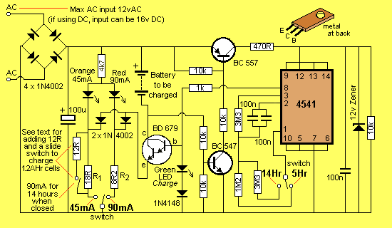
Rechargeable batteries are very popular for use in all sorts of devices, especially those requiring a high current.
The most common type of cell is the AA or penlight and although thousands have been sold, there are very few low-cost chargers to keep them in tip-top condition.
Most of them simply charge them at the slow rate and never turn off - you have to remember. Charging a cell for longer than necessary reduces its life so it’s important to cease the charging operation when the time is up.
To solve this problem we have designed an automatic charger to charge any number of AA cells, from 1 to 8 and turn off the power when the cells are charged.
When designing this project we assumed two things:
1. The user will only be charging AA cells, and
2. The cells will be almost totally discharged.
This will normally be the case as most nicads are used until the equipment starts to falter, such as a toy car going slow or a radio starting to distort. This is when the cells must be removed and recharged as it is an indication that one of the cells has reached its point of complete discharge and any further use will allow current to flow through the cell in the reverse direction and damage it.
All our discussion in this article will concentrate on the AA cell as the charger is specifically designed for this type of cell.
However C cells can be charged, simply by charging them at the 5 hour rate for two complete cycles. Just disconnect and re-connect when the first 5-hour timing is up.
This keeps the circuit simple and prevents possible overcharging of any of the cells, if you are alternately charging AA and C cells.
There are currently two types of AA nicad cells on the market.
The ampere-hour capacity of the old-style cell is 450mAHr. Some of them are 500mAHr, 550mAHr or 600mAHr.
Newer AA cells are 1.1AHr or 1.2AHr. Fortunately, most cells have the amp hour rating on them and this will help you set the charge-rate and/or time.
The first thing you cannot do is combine old-style cells with the new style. If you do, you will either over-charge the old-style ones or only partially charge the new ones. Stick to one type of cell at a time and select the time and charge-rate you require.
If you intend to charge the 1.2Ahr cells, we have added two components on the circuit diagram to change the charging current to 90mA for 14 hours to cater for this type of cell. This consists of a 12R resistor and slide switch that can be mounted on the top of the box and labelled 600mAHr when in one position and 1.2AHr in the other position. We have not provided a quick charge facility for the 1.2AHr cells.
Instead of adding this switch, you can simply give them three cycles at the 5 hour-rate or two cycles at the 14 hour rate.
We have lumped all the old-style cells in to one category as the difference between a 450mAHr cell and 600mAHr will be very small as far as the charging is concerned and in use you will hardly detect the difference as you will rarely be able to use all the energy in a cell.
The full capacity of a 450mAHr or 600mAHr cell is only obtained when the cell is discharged under fairly low laboratory conditions such as 10 - 15mA. Most toys and radios take 2 - 30 times more than this and the amp-hour capacity you get from the cell falls considerably as the current-demand increases.
Every cell and every condition is different but you can easily reduce the Amp-hour capacity to 200 - 300mAHr if you use it in something that takes 200 - 300mA.
That's why you only get one or two hour's life (or even less) out of a set of cells when you are using them in a toy such as a remote control car.
However the 1.1 and 1.2AHr cells will provide twice the energy of the old-style cells, under the same conditions.
No matter which type of cell you choose, the cost of powering high-performance toys will drop considerably by using rechargeable types.
And with this charger you can keep them fully charged without over or under charging.
To get the best performance out of rechargeable cells you must remember four things:
1. Cells must not be left in an uncharged state,
2. They must not be overcharged,
3. They must not be totally discharged (cell voltage must remain above 1v) and
4. They must not be discharged at more than 500mA (for more than a few seconds).
Any abuse of these rules will reduce the capacity of the cell. Nicads (and all their closely allied variations) also have another unusual characteristic that reduces the capacity. It's called "memory."
If you recharge a cell that is only say 25% discharged, the cell will think its new capacity is only 25% of the true value. Thus you will only be able to get 25% of its energy before the cell starts to falter.
This means it is very important to almost fully discharge a cell before starting the charging process.
Some of the new cells do not have this "memory" problem but their cost at the moment is more than twice the older style cells - so, it's the old saying: you get what you pay for. This project will enable you to care for AA cells and even rejuvenate some of them that have generated a memory. If a cell with a memory is discharged fully and charged completely, over a number of cycles, its poor performance can be improved and some can be restored to near full capacity. There is another device, called a nicad Zapper, that will rejuvenate some of the cells that have developed an internal fault, such as a short, that prevents it from receiving a charge. Now back to our circuit.
HOW THE CIRCUIT WORKS
The heart of the circuit is a 4541 timing chip. It has a built-in oscillator that requires only two external components for timing. A chain of sixteen binary dividers inside the chip is capable of producing a division of 65,536. With this we can produce very long time delays by making the internal clock of the chip a low-frequency oscillator and using it to clock the divider chain.
The other feature of this project is the constant-current charging circuit that allows you to fit any number of cells, up to 8, in the charging holder. Some chargers only accept 1,2 or 4 cells at a time while ours will accept any number providing the unused parts of the holder are connected with a jumper lead to make a complete charging path.
The BC 547 and BC 557 in the Automatic charger detect when a battery has been fitted to the circuit and turn on the 4541 timing chip. The green "Charge" LED comes on to show the battery is charging.
The orange LED shows you have selected the 14 hour rate and the red LED indicates you have selected the 5 hour rate.
CHARGING
During charging, no gases are generated. However during the latter part of the charge-cycle, during overcharge and during heavy discharge, hydrogen and oxygen gases are generated as well as electrolyte fumes. These gases can normally react with each other and not increase the pressure inside the cell however if they are produced at a fast rate, this equilibrium condition cannot be maintained and the pressure inside the cell builds up.
A pressure release valve is built into the cell but any gases that escape will include some of the electrolyte in the fumes and the cell will eventually dry out. For this reason it is important to limit the charging cycle.
ADAPTING THE CHARGER
The charger can be adapted to charge AA, C, or D cells or any combination of these by modifying the circuit slightly or by adding extra constant-current sections as shown in the circuit diagram below.
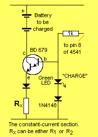 It will even charge 1.2AHr or 1.9AHr Gel cells of the 12v type as used in alarm systems, simply by making sure the rail voltage is above 18v, (but not more than 22v) to take into account the 3v minimum voltage drop across the BD 679 transistor.
If you want to charge only C or D cells, the circuit can be modified by changing the current-determining resistors R1 and R2 as follows:
The wattage of the resistors in the above table will have to be taken into account due to the high current that will be flowing through them The following table shows you how to "make-up" the resistors:
If you want to charge AA, C and D cells, you can add extra circuitry consisting of the constant-current section shown above to cater for the C and D cells.
To charge these cells, the BD 679 transistor will have to be heat-sinked with a larger heat-sink than is provided in the kit and the plug pack will have to be upgraded.
For a C cell, the 14 hour rate is 150mA and the 5 hour rate is 300mA. For a D cell, the 14 hour rate is 350mA and 700mA for the 5 hour rate.
Most plug packs have very poor regulation and the output voltage will drop considerably when full current is delivered. You will need a 500mA plug pack to deliver 350mA and a 1amp plug pack to deliver 700mA. Otherwise a 300mA or 400mA plug pack will be sufficient for the AA version.
Alternatively you can charge C and D cells with the original circuit by giving these cells two or three charge-cycles as show in the following table:
When choosing a plug pack, you must be careful not to supply the circuit with more than 15v AC as this becomes 22v DC when rectified and will create extra heat loss in the transistor.
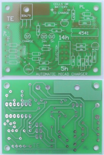
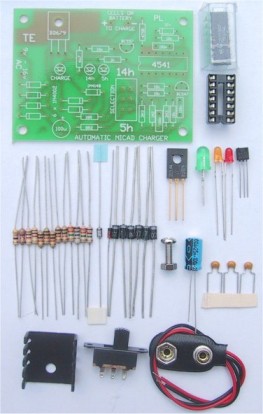
CONSTRUCTION
All the components fit on the PC board shown on the previous page with the small metal heat-sink fitted to the transistor.
Take care with the orientation of the diodes, LEDs transistors and electrolytic. Don't get the BC 547 and BC 557 mixed up and note; that the BD 679 has the metal face down and the writing up.
Fit all the rest of the components, remembering to fit the IC socket so that the cut-out at one end indicates pin 1. Fit the chip and the board is complete.
Solder the lead from the plug pack to the AC input terminals and connect a battery snap to the output terminals to take a 4-cell battery holder.
All you need to do is plug in the plug pack. The 5Hr or 14Hr LED will come on and the charge LED will come on when the cells are fitted to the holder.
Keep watching the charge LED. It will go out after the 5 or 14 hour period and your cells are ready for use.
TESTING
Remove one cell from the battery holder and measure the current being delivered to the other three cells. It should be about 45mA for the 14 hour rate or 90mA for the 5Hr rate.
If you have the switch and 12R fitted for the high performance 1.2AHr AA cells, the 14Hr current will be about 90mA.
You can charge up to 8 cells in series at a time however you must remember that to do this you need 17v - 18v on the supply rail. The same applies to 12v gel cells.
It is best to keep everything simple by charging one set of cells at a time and using two or more time-cycles to charge the larger cells. This way you won't overtax our little charger.
Adjustable power supply with charger

Notes
This power supply has adjustable and charger output. The charger circuit can be use for cellular phone. The adjustable output serves as multipurpose power supply. It can handle a 1 ampere current. The 317 must have a heat sink.
PCB Layout

Parts List
Semiconductor:
LM 317 - 1pc
LED - 1pc
1N 4001 - 8pcs
Capacitors:
25V/470uF - 1pc
25V/10 uF - 1pc
Resistors:
1k, 1/2W - 1pc
220R , 1/2W - 1pc
5kR Potentiometer - 1pc
Others:
1Ampere, Multi-tap Transformer - 1pc
AC Chord - 1pc
Casing - 1pc
#22 Stranded Wire - 3m
Heatsink for TO220
Most AC motors are three-phase or single-phase. Inside a three-phase motor there is a stator made of three pairs of coils and a rotor that houses a permanent magnet or a set of windings. The stator coils are supplied by a three-phase power line, featuring a phase angle shift of 120°. Each coil puts out an alternating magnetic field depending on the direction of the current flow. Since the coils work together they generate a rotating magnetic field, which lets the motor spin.
In a synchronous motor a permanent magnet spins at the synchronous speed of the rotating magnetic field, which depends on the supply frequency.
In an asynchronous motor there is a set of rotor windings shorted or closed through resistors.
The rotor will never reach the synchronous speed, otherwise the e.m.f. induced in the rotor windings would be null.
A single-phase motor works due to the same principle. The stator houses two sets of coils. One of them is connected in series with a capacitor, so there are two currents featuring a phase shift of about 90°. In other words it is a sort of two-phase power line.
The coils connected with the capacitor often switch off once the motor spins in the correct direction, so they are called start coils.
Q . IIII CAMERA
In 1984 I made a camera trigger to capture transient phenomena. I had a Mamiya ZE 35mm camera and Mamiyalite ZE flash unit. Typical for bodies of its time, the only means of remotely triggering the camera was the cable release socket built into its shutter release button. This was meant to be used with a purely mechanical cable; it let you operate the shutter release from a small distance away, and in a manner that avoided introducing vibration to the camera at the moment a picture was taken. 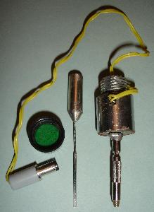 My solution for releasing the shutter electrically was to make a solenoid trigger. I rewound the coil of a small solenoid so that it would produce the necessary force when operated at 9V. It was a retraction type solenoid, meaning that applying current to it pulled the armature in. I wanted an extension solenoid, so I drilled a hole in the rear of it. I removed the camera end from a cable release - the part that screws into the cable release hole - and soldered it to the rear. I drilled a hole in the end of the armature, cut the pusher end off of the cable that was part of the release, soldered that into the armature, and then fed the pusher down through the solenoid and out the end of the cable release. The whole thing was light enough that I could simply screw it onto the shutter release of the camera and it would be supported without depressing the button. The other end of the solenoid was threaded for mounting in the way it was originally designed for. I found a cap that would fit this thread. This turned out to be particularly useful, because if set for automatic exposure, the camera required that the shutter release be partially depressed for long enough for it to do its calculation. If the shutter release was simply slammed down as fast as the solenoid did it, the shutter was released instantly and with incorrect exposure. By adjusting how far I screwed the cap down I could make the shutter release be initially depressed far enough to activate the camera.
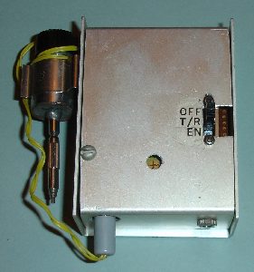
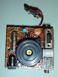 To operate the solenoid I made a circuit that would briefly apply current to it when triggered. It also had a “test” position that would operate a sounder instead of the solenoid, to facilitate setup. I ended up using this system mainly for taking pictures of rockets lifting off.
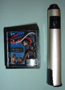
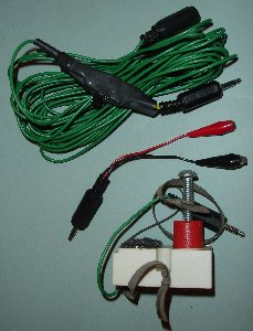 The devices that I used with the trigger included hardwired circuits and an ultrasonic remote. The ultrasonic remote is at left. I made it with a pair of surplus 40 kHz transducers. The green extension cord at right has an inline switch to set whether devices plugged into the mini jack on the end operate as normally-closed or normally-open triggers. The device with the bolt was used to take the tennis-ball cannon pictures below. No, I don't yet have any of the other (more successful) pictures I took with this system scanned!


Construction of the Mk1 Receiver
this page so that the valid data output from the decoder chip is used by the Stamp to detect when valid data is present. This is to improve compatibility with other decoder chips you might want to use. For example, I have an infra-red remote control kit that uses a different decoder chip. Its outputs are maintained after the control button has been released, so the valid data output must be used to determine if a switch is actually pressed.
The changes to the Stamp program have made it about 40 bytes smaller too!
The receiver requires 8.5mA, plus 1.5mA for each LED (individual or segment) that is lit for a maximum of up to 23mA. In practice it is between 13 and 16mA. Pressing a button on the remote transmitter causes the receiver to consume an extra 0.2mA. In the 'power saving' mode the PBASIC 'nap' instruction is used in combination with turning all the LEDs off to reduce power consumption to 4mA. The battery should last about 30 hours of on-time.
The PBASIC program itself takes up 272 bytes, constant data 28 bytes, and it uses 4 bytes of RAM. Plenty of room (22 bytes of RAM and 1748 bytes of EEPROM) for enhancements...
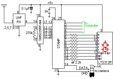
The circuit is very simple. The pre-built UHF receiver module outputs a bit stream to the decoder chip. The decoder chip looks for repeats of valid sequences. When it decides a valid data transmission has been received, it sets pin 17 (valid data) high and the data appears on pins 10-13.
The Stamp monitors the valid data bit from the decoder. As soon as it becomes high (1), the Stamp knows that a remote button has been pressed.
The SM5035RF-M4 decoder and matching SM5023RF encoder support an eight-bit trinary encoding to distinguish different sets of receivers and transmitters. Each of the eight pins may be left floating, connected to ground, or connected to +5v for a total of 38 = 6561 codes. Leave all the pins floating until you have confirmed it working, then connect one or more pins to ground or +5v, making sure the transmitter and receiver are configured identically.
Note that the circuit diagram has my particular LED display. Most likely yours will be different - make sure you know the correct pinouts for your display! My circuit is based on a common anode LED display. If yours is common cathode, see below for the changes required to make it work.
If you live outside Australia I can't help - I assume you know what's available in your area.
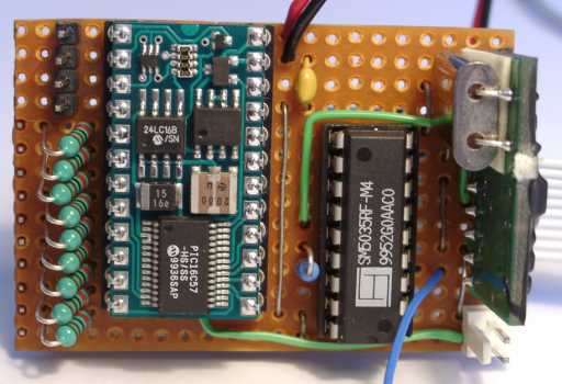
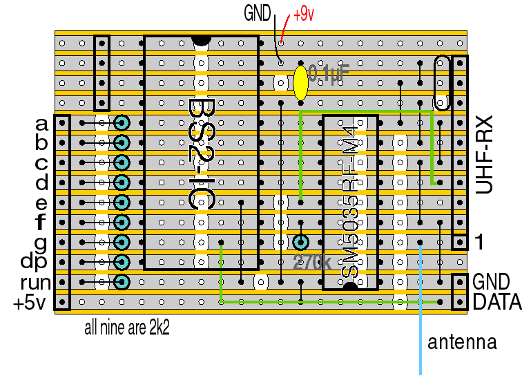
The receiver is built on 2.54mm (0.1") pitch veroboard, using 21×14 holes (55×37mm). The track strips are in the long direction of the board and need to be 'cut' as shown below. I used a drill to remove the track layer (there are 45 'cuts'):
Install the nine 2k2 resistors, but keep the trimmed legs. The resistors are vertically mounted to leave room for the Stamp socket to fit.
Now install the nine bare links and the bottom insulated link. Use the resistor legs you kept from the previous step for the bare links. The second insulated link is put on after you've done the IC sockets.
Put on the IC sockets - the notch of the Stamp socket points up, the other points down.
You can put on the other insulated link now - bend it so it lies flat against the board and goes around the 18-pin socket.
Solder on the four-pin header at the top left, leaving a gap between the it and the 24-pin socket to allow the cable connector room to fit on.
Solder the 270k resistor next to the 18-pin socket, and the 0.1µF capacitor up next to the 24-pin socket.
Solder the two-pin header at the bottom right of the board.
Turn the board over and solder the right angle 10 pin header plug with the pins facing into the board. The idea is to glue the socket it plugs into to the box you'll put the receiver in, then plugging the receiver into the socket also locates the receiver and stops it moving about.
Make up the 10 pin header socket so it connects to your 7-segment LED display. Arrange the wiring so that pins 5-11 of the Stamp are segments a-g, and pin 12 of the Stamp is the decimal point. My display has a second decimal point that connects to pin 16 of the Stamp. If yours doesn't have a second decimal point (most don't), connect a separate LED.
Solder on the UHF receiver module - the crystal is at the top, then install the ICs - make sure they point the right way! The Stamp points up and the decoder chip points down.
You can solder the battery connection to the board. I would recommend the panel switch be used so you can easily turn it on and off - particularly if you put the receiver inside a plastic box!
The picture below shows the remote board, including the key fob and a CF card for scale. The blue wire is the antenna. The grey cable leaving the photo on the left reenters at the top right to show the camera serial connector. The plastic shroud that came with the 2.5mm stereo plug fouled on the camera casing, so I threw the shroud away and covered the plug with some heatshrink tubing. Refer to the circuit diagram and board layout graphics for cable connections. Make the outside braid of the cable the ground and the inner core the data. The tip of the stereo plug has nothing connected to it.
At this point, before you connect a battery, give your board a close examination, checking for bridged tracks or not-quite-soldered joints. Use a multimeter to check the resistance across pins 23 and 24 and across pins 21 and 23 of the Stamp. Make sure they aren't short-circuited. Make sure none of the Stamp I/O pins (5-20) are shorted to either ground (pin 23 of the Stamp) or the power (pin 21 of the Stamp).
If possible, try to get access to a current-limiting 'laboratory' power supply and limit the current to 30-40mA for testing. It's quite easy to 'blow up' the chips if you've made a mistake somewhere.
I would recommend disconnecting the LEDs (if you've used the connector) and hooking up your multimeter to measure the current drawn by the receiver when testing. When the power is first applied it will briefly (<1sec) draw quite a bit of current before settling down to about 8-9mA. If you have left the LEDs connected and they're on it could be up to 25mA. If your multimeter measures more than 25mA for longer than a second, disconnect the power and look for what the problem might be.
You can either make a special cable that goes between the Stamp and your computer, or you could solder a temporary DB9 connector directly to the board (you wouldn't need the four-pin header then).
The Stamp programming software can be downloaded from the Parallax web site. I would suggest using the Windows program (
Power up the receiver board and run the software. Select the 'Identify' option from the 'Run' menu. It should display a dialog showing the type of Stamp you have. If not, check your cable, serial settings, etc.
Assuming 'Identify' works, download my PBASIC program:
Happy remote controlling!
The real problem is that it would require substantial modifications to the PBASIC program. It is left as an exercise for the reader .
.
A slight problem is the resonator on the Stamp - it isn't very accurate. A good crystal based clock generator, divided down to 2Hz would make it easy for the PBASIC program to poll and keep good time.
There aren't enough Stamp pins to directly control three LEDs, so they would have to be connected serially using latching shift registers. Three Stamp pins could handle any number of displays!
KEYPAD
This is an enhanced 4 digit keypad which may be used with the Modular Alarm System.

Notes
The Keypad must be the kind with a common terminal and a separate connection for each key. On a 12-key pad, look for 13 terminals. The matrix type with 7 terminals will NOT do. The Alarm is set by pressing a single key. Choose the key you want to use and wire it to 'E'. Choose the four keys you want to use to switch the alarm off, and connect them to 'A B C & D'. Your code can include the non-numeric symbols. With a 12-key pad, over 10 000 different codes are available. Wire the common to R1 and all the remaining keys to 'F'. When 'E' is pressed, current through D2 and R9 switches Q5 on. The relay energises, and then holds itself on by providing base current for Q5 through R10. The 12-volt output is switched from the "off " to the "set " terminal, and the LED lights. To switch the Alarm off again it is necessary to press A, B, C & D in the right order. The IC is a quad 2-input AND gate, a Cmos 4081. These gates only produce a high output when both inputs are high. Pin 1 is held high by R5. This 'enables' gate 1, so that when 'A' is pressed, the output at pin 3 will go high. This output does two jobs. It locks itself high using R2 and it enables gate 2 by taking pin 5 high. The remaining gates operate in the same way, each locking itself on through a resistor and enabling its successor. If the correct code is entered, pin 10 will switch Q4 on and so connect the base of Q5 to ground. This causes Q5 to switch off and the relay to drop out. Any keys not wired to 'A B C D or E' are connected to the base of Q3 by R7. Whenever one of these 'wrong' keys is pressed, Q3 takes pin 1 low. This removes the 'enable' from gate 1, and the code entry process fails. If 'C' or 'D' is pressed out of sequence, Q1 or Q2 will also take pin 1 low, with the same result. You can change the code by altering the keypad connections. If you need a more secure code use a bigger keypad with more 'wrong' keys wired to 'F'. A 16-key pad gives over 40 000 different codes. All components are shown lying flat on the board; but some are actually mounted upright. The links are bare copper wires on the component side. Two of the links must be fitted before the IC.
Veroboard Layout


constructed a 'magic wand'
which will display a message in mid air when waved in front of you.
The wand is not very easy to see in daylight, but many people can see it.
I have constructed this with little components so it is very cheap.

NOTE: MCLR Pin5 should be connected to +vdc (+5v DC)
This is a small probe box and cost approximately 1GBP.
I drilled 5 holes for the LED's and made a small PCB to fit inside.
The box is *Just* big enough to squeese a 9V battery in, which supplies the PCB with the power.
The scrolling sensing is done by a tilt switch/ push button.
If a tilt switch is used, you will have to juggle with it for optimal performance.
In place of the tilt switch, you could put a button mounted on the case, which when pressed will triggger off the display.
the steps below, and the scroller will work.
Steps:
1) Get all of the components (see below)
2) Assemble the components on a PCB or Veroboard.
Use the circuit diagram to build it.
.... 2.1) Place the smallest pieces on the board first.
Do it in height order. i.e links first then resistors caps... Put the programmed microchip in first.
.... 2.2) Program the microcontroller with the message.asm file.
.... 2.3) Place the programmed chip into the board.
The chip should be set to Watch Dog Timer off (WDT) and oscillator mode RC.
You can download pictures of the Simple PIC programmer from my web site (www.bazginge.demon.co.uk)
3) Drill all of the holes in the box.
The holes should be:
5x LED hole
1x button hole(optional)
1x off switch
4) Push the PCB into the box, with the LED's pushed into the holes drilled.
Attach the PCB to the bottom of the box
with either tape/velcro or PCB spacers depending on the height of the LEDS from the bottom of box.
5) Put battery in box making sure that it is held in tightly.
6) Put the top onto the box. Turn on and wave around
R1 100K Metal film 0.5%
R2 12K
Capacitors
C1 100n Ceramic cap
C2 100n Ceramic cap
C3 100uF Electrolytic
C4 10pF Ceramic cap
Semiconductors
IC1 PIC16C84 04 (4Mhz)
IC2 LM7805 voltage regulator
Misc
5x Red LED
1x push to make switch
1x toggle/slide switch
Software
The software is very simple indeed. the are mainly four parts to my code.
1) The declarations
2) The message to be scrolled
3) The letter output routines
4) The wait routine
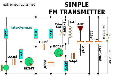
This FM transmitter (FM Tx) is about the simplest and most basic FM Tx it is possible to build and have a useful transmitting range. It is surprisingly powerful despite its small component count and 3V operating voltage. It will easily penetrate over three floors of an apartment building and go over 300 meters in the open air. The circuit we use is based on a proven Australian design. It may be tuned anywhere in the FM band. Or it may be tuned outside the commercial M band for greater privacy. (Of course this means you must modify your FM radio to be able to receive the transmission or have a broad-band FM receiver.) The output power of this FM Tx is below the legal limits of many countries (eg, USA and Australia). However, some countries may ban ALL wireless transmissions without a license. It is the responsibility of the builder to check the legal requirements for the operation of this circuit and to obey them.
The circuit is basically a radio frequency (RF) oscillator that operates around 100 MHz. Audio picked up and amplified by the electret microphone is fed into the audio amplifier stage built around the first transistor. Output from the collector is fed into the base of the second transistor where it modulates the resonant frequency of the tank circuit (the 5 turn coil and the trimcap) by varying the junction capacitance of the transistor. Junction capacitance is a function of the potential difference applied to the base of the transistor. The tank circuit is connected in a Colpitts oscillator circuit.
Place the transmitter about 10 feet from a FM radio. Set the radio to somewhere about 89 – 90 MHz. Walk back to the Fm Tx and turn it on. Spread the winding of the coil apart by approximately 1mm from each other. No coil winding should be touching another winding. Use a small screw driver to tune the trim cap. Remove the screwdriver from the trim screw after every adjustment so the LC circuit is not affected by stray capacitance. Or use a plastic screwdriver. If you have difficulty finding the transmitting frequency then have a second person tune up and down the FM dial after every adjustment. One full turn of the trim cap will cover its full range of capacitance from 6pF to 45pF. The normal FM band tunes in over about one tenth of the full range of the tuning cap. So it is best to adjust it in steps of 5 to 10 degrees at each turn. So tuning takes a little patience but is not difficult. The reason that there must be at least 10 ft. separation between the radio and the Tx is that the Tx emits harmonics; it does not only emit on one frequency but on several different frequencies close to each other
You may experiment with using 6V or 9V with the circuit to see how this increases the range of the transmitter. The sensitivity may be increased by lowering the 22K resistor to 10K.

============== De electronics compasses circulate ma the matic ===============
The most common type of cell is the AA or penlight and although thousands have been sold, there are very few low-cost chargers to keep them in tip-top condition.
Most of them simply charge them at the slow rate and never turn off - you have to remember. Charging a cell for longer than necessary reduces its life so it’s important to cease the charging operation when the time is up.
To solve this problem we have designed an automatic charger to charge any number of AA cells, from 1 to 8 and turn off when the cells are charged.
Two photos of the Automatic AA Nicad Charger
|
| Automatic AA Nicad Battery Charger Circuit |
Rechargeable batteries are very popular for use in all sorts of devices, especially those requiring a high current.
The most common type of cell is the AA or penlight and although thousands have been sold, there are very few low-cost chargers to keep them in tip-top condition.
Most of them simply charge them at the slow rate and never turn off - you have to remember. Charging a cell for longer than necessary reduces its life so it’s important to cease the charging operation when the time is up.
To solve this problem we have designed an automatic charger to charge any number of AA cells, from 1 to 8 and turn off the power when the cells are charged.
When designing this project we assumed two things:
1. The user will only be charging AA cells, and
2. The cells will be almost totally discharged.
This will normally be the case as most nicads are used until the equipment starts to falter, such as a toy car going slow or a radio starting to distort. This is when the cells must be removed and recharged as it is an indication that one of the cells has reached its point of complete discharge and any further use will allow current to flow through the cell in the reverse direction and damage it.
All our discussion in this article will concentrate on the AA cell as the charger is specifically designed for this type of cell.
However C cells can be charged, simply by charging them at the 5 hour rate for two complete cycles. Just disconnect and re-connect when the first 5-hour timing is up.
| Automatically charges AA cells at 5Hr rate or 14Hr rate. Charges 600mAHr AA cells and 1.2AHr AA cells. |
There are currently two types of AA nicad cells on the market.
| Also Required: 8.5v AC 400mA plug pack or 15v AC 1amp transformer Use 9v5 tap for up to 8 x AA cells or 15v tap for 12v Gel cell battery. |
Newer AA cells are 1.1AHr or 1.2AHr. Fortunately, most cells have the amp hour rating on them and this will help you set the charge-rate and/or time.
The first thing you cannot do is combine old-style cells with the new style. If you do, you will either over-charge the old-style ones or only partially charge the new ones. Stick to one type of cell at a time and select the time and charge-rate you require.
If you intend to charge the 1.2Ahr cells, we have added two components on the circuit diagram to change the charging current to 90mA for 14 hours to cater for this type of cell. This consists of a 12R resistor and slide switch that can be mounted on the top of the box and labelled 600mAHr when in one position and 1.2AHr in the other position. We have not provided a quick charge facility for the 1.2AHr cells.
Instead of adding this switch, you can simply give them three cycles at the 5 hour-rate or two cycles at the 14 hour rate.
We have lumped all the old-style cells in to one category as the difference between a 450mAHr cell and 600mAHr will be very small as far as the charging is concerned and in use you will hardly detect the difference as you will rarely be able to use all the energy in a cell.
The full capacity of a 450mAHr or 600mAHr cell is only obtained when the cell is discharged under fairly low laboratory conditions such as 10 - 15mA. Most toys and radios take 2 - 30 times more than this and the amp-hour capacity you get from the cell falls considerably as the current-demand increases.
Every cell and every condition is different but you can easily reduce the Amp-hour capacity to 200 - 300mAHr if you use it in something that takes 200 - 300mA.
That's why you only get one or two hour's life (or even less) out of a set of cells when you are using them in a toy such as a remote control car.
However the 1.1 and 1.2AHr cells will provide twice the energy of the old-style cells, under the same conditions.
No matter which type of cell you choose, the cost of powering high-performance toys will drop considerably by using rechargeable types.
And with this charger you can keep them fully charged without over or under charging.
To get the best performance out of rechargeable cells you must remember four things:
1. Cells must not be left in an uncharged state,
2. They must not be overcharged,
3. They must not be totally discharged (cell voltage must remain above 1v) and
4. They must not be discharged at more than 500mA (for more than a few seconds).
Any abuse of these rules will reduce the capacity of the cell. Nicads (and all their closely allied variations) also have another unusual characteristic that reduces the capacity. It's called "memory."
If you recharge a cell that is only say 25% discharged, the cell will think its new capacity is only 25% of the true value. Thus you will only be able to get 25% of its energy before the cell starts to falter.
This means it is very important to almost fully discharge a cell before starting the charging process.
Some of the new cells do not have this "memory" problem but their cost at the moment is more than twice the older style cells - so, it's the old saying: you get what you pay for. This project will enable you to care for AA cells and even rejuvenate some of them that have generated a memory. If a cell with a memory is discharged fully and charged completely, over a number of cycles, its poor performance can be improved and some can be restored to near full capacity. There is another device, called a nicad Zapper, that will rejuvenate some of the cells that have developed an internal fault, such as a short, that prevents it from receiving a charge. Now back to our circuit.
HOW THE CIRCUIT WORKS
The heart of the circuit is a 4541 timing chip. It has a built-in oscillator that requires only two external components for timing. A chain of sixteen binary dividers inside the chip is capable of producing a division of 65,536. With this we can produce very long time delays by making the internal clock of the chip a low-frequency oscillator and using it to clock the divider chain.
The other feature of this project is the constant-current charging circuit that allows you to fit any number of cells, up to 8, in the charging holder. Some chargers only accept 1,2 or 4 cells at a time while ours will accept any number providing the unused parts of the holder are connected with a jumper lead to make a complete charging path.
The BC 547 and BC 557 in the Automatic charger detect when a battery has been fitted to the circuit and turn on the 4541 timing chip. The green "Charge" LED comes on to show the battery is charging.
The orange LED shows you have selected the 14 hour rate and the red LED indicates you have selected the 5 hour rate.
CHARGING
During charging, no gases are generated. However during the latter part of the charge-cycle, during overcharge and during heavy discharge, hydrogen and oxygen gases are generated as well as electrolyte fumes. These gases can normally react with each other and not increase the pressure inside the cell however if they are produced at a fast rate, this equilibrium condition cannot be maintained and the pressure inside the cell builds up.
A pressure release valve is built into the cell but any gases that escape will include some of the electrolyte in the fumes and the cell will eventually dry out. For this reason it is important to limit the charging cycle.
ADAPTING THE CHARGER
The charger can be adapted to charge AA, C, or D cells or any combination of these by modifying the circuit slightly or by adding extra constant-current sections as shown in the circuit diagram below.
If you want to charge only C or D cells, the circuit can be modified by changing the current-determining resistors R1 and R2 as follows:
C cell
|
D cell
| |
14Hr rate
(R1) |
4R7
|
2R2
|
5Hr rate
(R2) |
2R7
|
1R0
|
The current-determining resistors for “C” and "D" cells
|
4R7 = two 10R resistors in parallel
|
2R2 = 4 x 10R resistors in parallel
|
2R7 = Four 10R resistors in parallel
|
1R = two 2R2 10R resistors in parallel
|
To charge these cells, the BD 679 transistor will have to be heat-sinked with a larger heat-sink than is provided in the kit and the plug pack will have to be upgraded.
For a C cell, the 14 hour rate is 150mA and the 5 hour rate is 300mA. For a D cell, the 14 hour rate is 350mA and 700mA for the 5 hour rate.
Most plug packs have very poor regulation and the output voltage will drop considerably when full current is delivered. You will need a 500mA plug pack to deliver 350mA and a 1amp plug pack to deliver 700mA. Otherwise a 300mA or 400mA plug pack will be sufficient for the AA version.
Alternatively you can charge C and D cells with the original circuit by giving these cells two or three charge-cycles as show in the following table:
CHARGING:
|
5 Hour rate:
|
| C cells |
2 time-cycles
|
| D cells |
5 time-cycles
|
The PCB, showing the overlay and the track work
|
Automatic AA Nicad Charger kit, showing all the components
|
PARTS LIST
|
| 1 - 8R2 1 - 18R 1 - 470R 1 - 1k 1 - 4k7 5 - 10k 1 - 1M2 2 - 3M3 3 - 100n monoblock capacitors 1 - 100u 25v PC mount electrolytic 1 - 1N 4148 diode 6 - 1N 4004 power diodes 1 - 12v Zener diode 400mW 1 - BC 547 transistor 1 - BC 557 transistor 1 - BD 679 transistor 1 - 4541 IC 1 - 14 pin IC socket 1 - 3mm orange LED 1 - 3mm red LED 1 - 5mm green LED 1 - battery snap 1 - DPDT slide-switch 1 - 10cm tinned copper wire 1 - Auto Nicad Charger PC board |
Extras:
|
| 1 - plug pack 1 - 2 cell or 4 cell AA battery holder 1 - 12R (for charging 1.2AHr cells) 1 - slide switch 1 - 3cm x 5cm heat-sink 1 - 12mm bolt with nut for heat-sink |
CONSTRUCTION
All the components fit on the PC board shown on the previous page with the small metal heat-sink fitted to the transistor.
Take care with the orientation of the diodes, LEDs transistors and electrolytic. Don't get the BC 547 and BC 557 mixed up and note; that the BD 679 has the metal face down and the writing up.
Fit all the rest of the components, remembering to fit the IC socket so that the cut-out at one end indicates pin 1. Fit the chip and the board is complete.
Solder the lead from the plug pack to the AC input terminals and connect a battery snap to the output terminals to take a 4-cell battery holder.
All you need to do is plug in the plug pack. The 5Hr or 14Hr LED will come on and the charge LED will come on when the cells are fitted to the holder.
Keep watching the charge LED. It will go out after the 5 or 14 hour period and your cells are ready for use.
TESTING
Remove one cell from the battery holder and measure the current being delivered to the other three cells. It should be about 45mA for the 14 hour rate or 90mA for the 5Hr rate.
If you have the switch and 12R fitted for the high performance 1.2AHr AA cells, the 14Hr current will be about 90mA.
You can charge up to 8 cells in series at a time however you must remember that to do this you need 17v - 18v on the supply rail. The same applies to 12v gel cells.
It is best to keep everything simple by charging one set of cells at a time and using two or more time-cycles to charge the larger cells. This way you won't overtax our little charger.
Adjustable power supply with charger
This power supply has adjustable and charger output. The charger circuit can be use for cellular phone. The adjustable output serves as multipurpose power supply. It can handle a 1 ampere current. The 317 must have a heat sink.
PCB Layout
Parts List
Semiconductor:
LM 317 - 1pc
LED - 1pc
1N 4001 - 8pcs
Capacitors:
25V/470uF - 1pc
25V/10 uF - 1pc
Resistors:
1k, 1/2W - 1pc
220R , 1/2W - 1pc
5kR Potentiometer - 1pc
Others:
1Ampere, Multi-tap Transformer - 1pc
AC Chord - 1pc
Casing - 1pc
#22 Stranded Wire - 3m
Heatsink for TO220
| AC electric motor working principle |
Most AC motors are three-phase or single-phase. Inside a three-phase motor there is a stator made of three pairs of coils and a rotor that houses a permanent magnet or a set of windings. The stator coils are supplied by a three-phase power line, featuring a phase angle shift of 120°. Each coil puts out an alternating magnetic field depending on the direction of the current flow. Since the coils work together they generate a rotating magnetic field, which lets the motor spin.
In a synchronous motor a permanent magnet spins at the synchronous speed of the rotating magnetic field, which depends on the supply frequency.
In an asynchronous motor there is a set of rotor windings shorted or closed through resistors.
The rotor will never reach the synchronous speed, otherwise the e.m.f. induced in the rotor windings would be null.
A single-phase motor works due to the same principle. The stator houses two sets of coils. One of them is connected in series with a capacitor, so there are two currents featuring a phase shift of about 90°. In other words it is a sort of two-phase power line.
The coils connected with the capacitor often switch off once the motor spins in the correct direction, so they are called start coils.
 Single-phase motor circuit schematic |
Q . IIII CAMERA
Electronic Shutter Release
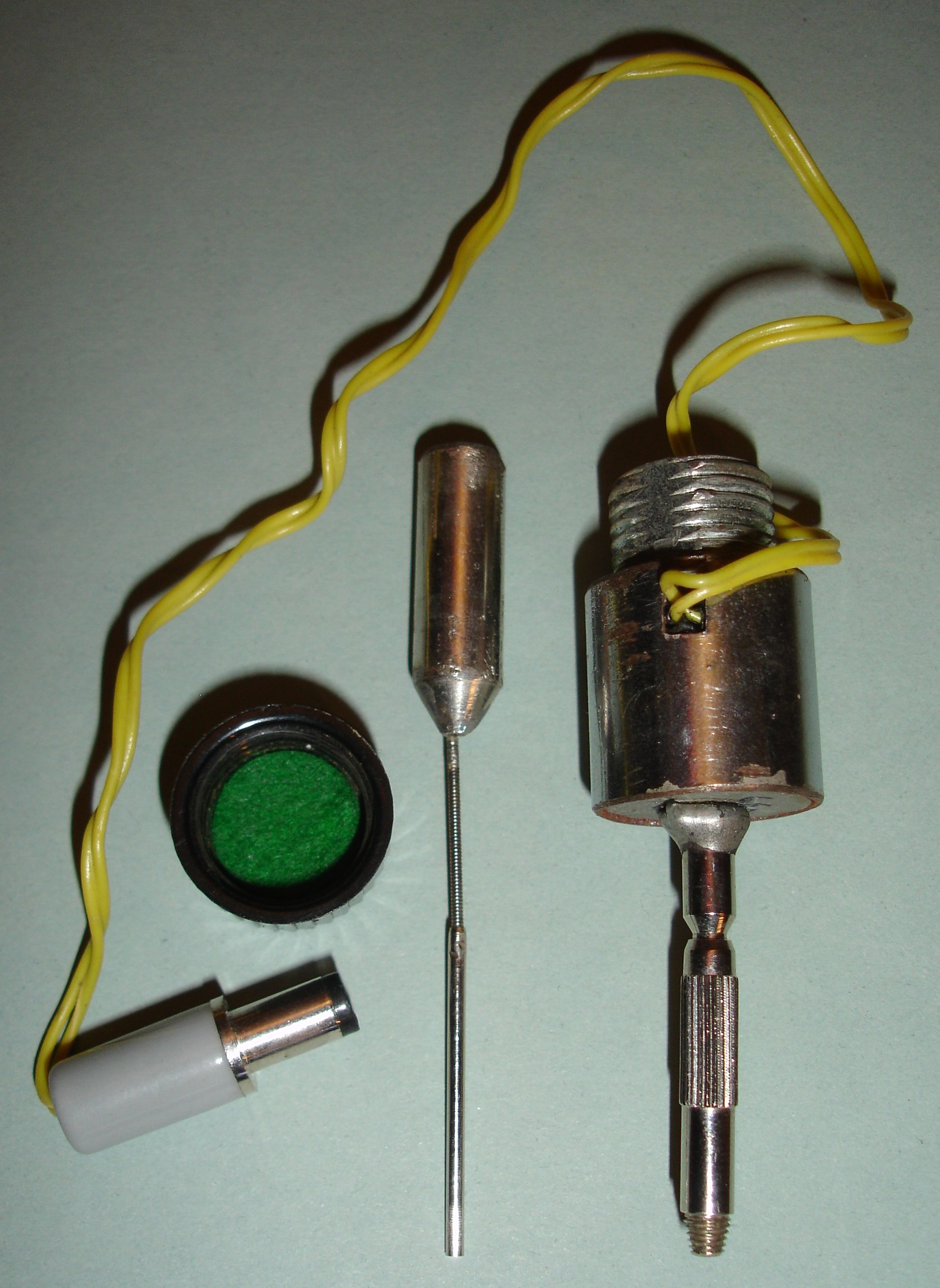 My solution for releasing the shutter electrically was to make a solenoid trigger. I rewound the coil of a small solenoid so that it would produce the necessary force when operated at 9V. It was a retraction type solenoid, meaning that applying current to it pulled the armature in. I wanted an extension solenoid, so I drilled a hole in the rear of it. I removed the camera end from a cable release - the part that screws into the cable release hole - and soldered it to the rear. I drilled a hole in the end of the armature, cut the pusher end off of the cable that was part of the release, soldered that into the armature, and then fed the pusher down through the solenoid and out the end of the cable release. The whole thing was light enough that I could simply screw it onto the shutter release of the camera and it would be supported without depressing the button. The other end of the solenoid was threaded for mounting in the way it was originally designed for. I found a cap that would fit this thread. This turned out to be particularly useful, because if set for automatic exposure, the camera required that the shutter release be partially depressed for long enough for it to do its calculation. If the shutter release was simply slammed down as fast as the solenoid did it, the shutter was released instantly and with incorrect exposure. By adjusting how far I screwed the cap down I could make the shutter release be initially depressed far enough to activate the camera.
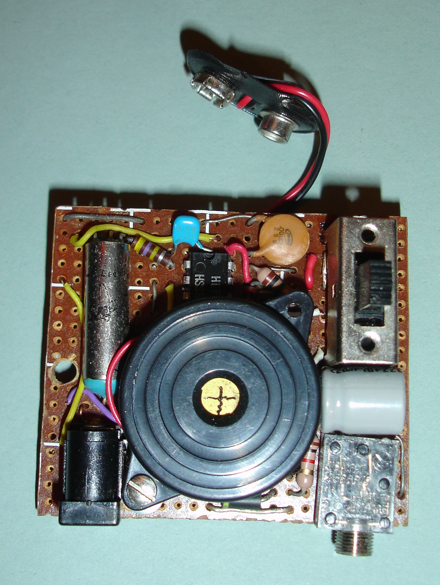 To operate the solenoid I made a circuit that would briefly apply current to it when triggered. It also had a “test” position that would operate a sounder instead of the solenoid, to facilitate setup. I ended up using this system mainly for taking pictures of rockets lifting off.
 The devices that I used with the trigger included hardwired circuits and an ultrasonic remote. The ultrasonic remote is at left. I made it with a pair of surplus 40 kHz transducers. The green extension cord at right has an inline switch to set whether devices plugged into the mini jack on the end operate as normally-closed or normally-open triggers. The device with the bolt was used to take the tennis-ball cannon pictures below. No, I don't yet have any of the other (more successful) pictures I took with this system scanned!
 Construction of the Mk1 Receiver
this page so that the valid data output from the decoder chip is used by the Stamp to detect when valid data is present. This is to improve compatibility with other decoder chips you might want to use. For example, I have an infra-red remote control kit that uses a different decoder chip. Its outputs are maintained after the control button has been released, so the valid data output must be used to determine if a switch is actually pressed.
The changes to the Stamp program have made it about 40 bytes smaller too!
Description
The remote control receiver is a custom design based on a pre-built 433MHz UHF radio receiver, a decoder chip and a BASIC Stamp. The Stamp is expensive, but easy to work with.The receiver requires 8.5mA, plus 1.5mA for each LED (individual or segment) that is lit for a maximum of up to 23mA. In practice it is between 13 and 16mA. Pressing a button on the remote transmitter causes the receiver to consume an extra 0.2mA. In the 'power saving' mode the PBASIC 'nap' instruction is used in combination with turning all the LEDs off to reduce power consumption to 4mA. The battery should last about 30 hours of on-time.
The PBASIC program itself takes up 272 bytes, constant data 28 bytes, and it uses 4 bytes of RAM. Plenty of room (22 bytes of RAM and 1748 bytes of EEPROM) for enhancements...
Circuit Diagram
The circuit is very simple. The pre-built UHF receiver module outputs a bit stream to the decoder chip. The decoder chip looks for repeats of valid sequences. When it decides a valid data transmission has been received, it sets pin 17 (valid data) high and the data appears on pins 10-13.
The Stamp monitors the valid data bit from the decoder. As soon as it becomes high (1), the Stamp knows that a remote button has been pressed.
The SM5035RF-M4 decoder and matching SM5023RF encoder support an eight-bit trinary encoding to distinguish different sets of receivers and transmitters. Each of the eight pins may be left floating, connected to ground, or connected to +5v for a total of 38 = 6561 codes. Leave all the pins floating until you have confirmed it working, then connect one or more pins to ground or +5v, making sure the transmitter and receiver are configured identically.
Note that the circuit diagram has my particular LED display. Most likely yours will be different - make sure you know the correct pinouts for your display! My circuit is based on a common anode LED display. If yours is common cathode, see below for the changes required to make it work.
Components
The sources given below are those most easily accessed in Australia. There are also (among others) RS Components and Farnell, but they are expensive and cater to industry rather than enthusiasts.If you live outside Australia I can't help - I assume you know what's available in your area.
| Quantity | Description | Sources (you should confirm the catalogue numbers below before spending your money) | ||
|---|---|---|---|---|
| Altronics | Dick Smith Electronics | Jaycar | ||
| 1 | Veroboard (check to make sure there are no gaps in the tracks, such as for a model number or something - there must be 21×14 clear tracks) | H 0714 | H 5614 | HP-9540 |
| 1 | BS-2 IC BASIC Stamp | Z 5520 | K 1404 | XS-5530 |
| 1 | SM5035RF-M4 remote control decoder | Oatley Electronics (contact them - it's a non-catalog item) | ||
| 1 | 433MHz UHF receiver module | Oatley Electronics (RX14) | ||
| 1 | 24 pin IC socket suitable for Stamp | P 0570 | P 4240 | PI-6506 |
| 1 | 18 pin IC socket suitable for SM5035RF-M4 | P 0567 | P 4180 | PI-6503 |
| 1 | 4 pin header | P 5430 | P 2726 | n/a |
| 1 | 10 pin header plug, right angle | P 5520 | n/a | HM-3430 |
| 1 | 10 pin header socket | P 5480 | n/a | HM-3410 |
| 1 | 2 pin header plug, straight | P 5492 | P 2731 (includes socket) | HM-3412 |
| 1 | 2 pin header socket | P 5472 | P 2731 (includes plug) | HM-3402 |
| 1 | 270k resistor | R 0616 | R 1134 | RR-0630 |
| 9 | 2k2 resistors | R 0566 | R 1082 | RR-0580 |
| 1 | 0.1µF capacitor, monolithic | R 2930 | R 2001 | RC-5490 |
| 1 | seven-segment LED display, common anode | Z 0191 | n/a | ZD-1857 |
| 1 | 9V battery snap | P 0455 | S 6100 | PH-9232 |
| 1 | 9V battery | S 4930 | S 3286 | SB-2395 |
| 1 | switch, panel mount (for power) | S 2010 | P 7610 | SS-0852 |
| 1 | 2.5mm stereo plug (to connect to camera) | n/a | P 1127 | PP-0103 |
| 1-2m | cable, single core, screened (to connect receiver to camera) | W 3010 | W 2030 | WB-1500 |
| 1 | short length (30mm) of 10mm heatshrink tubing | W 0915 | W 4116 | WH-5535 |
| 1 | length of wire for antenna, preferably solid conductor (690mm full wave, 345mm half wave, 172.5mm quarter wave) | junk box | ||
| 1 | miscellaneous hook-up wire | junk box | ||
Construction
Refer to the photo and layout diagram below while building to make sure you get things in the right spot. The receiver is built on 2.54mm (0.1") pitch veroboard, using 21×14 holes (55×37mm). The track strips are in the long direction of the board and need to be 'cut' as shown below. I used a drill to remove the track layer (there are 45 'cuts'):
Install the nine 2k2 resistors, but keep the trimmed legs. The resistors are vertically mounted to leave room for the Stamp socket to fit.
Now install the nine bare links and the bottom insulated link. Use the resistor legs you kept from the previous step for the bare links. The second insulated link is put on after you've done the IC sockets.
Put on the IC sockets - the notch of the Stamp socket points up, the other points down.
You can put on the other insulated link now - bend it so it lies flat against the board and goes around the 18-pin socket.
Solder on the four-pin header at the top left, leaving a gap between the it and the 24-pin socket to allow the cable connector room to fit on.
Solder the 270k resistor next to the 18-pin socket, and the 0.1µF capacitor up next to the 24-pin socket.
Solder the two-pin header at the bottom right of the board.
Turn the board over and solder the right angle 10 pin header plug with the pins facing into the board. The idea is to glue the socket it plugs into to the box you'll put the receiver in, then plugging the receiver into the socket also locates the receiver and stops it moving about.
Make up the 10 pin header socket so it connects to your 7-segment LED display. Arrange the wiring so that pins 5-11 of the Stamp are segments a-g, and pin 12 of the Stamp is the decimal point. My display has a second decimal point that connects to pin 16 of the Stamp. If yours doesn't have a second decimal point (most don't), connect a separate LED.
Solder on the UHF receiver module - the crystal is at the top, then install the ICs - make sure they point the right way! The Stamp points up and the decoder chip points down.
You can solder the battery connection to the board. I would recommend the panel switch be used so you can easily turn it on and off - particularly if you put the receiver inside a plastic box!
The picture below shows the remote board, including the key fob and a CF card for scale. The blue wire is the antenna. The grey cable leaving the photo on the left reenters at the top right to show the camera serial connector. The plastic shroud that came with the 2.5mm stereo plug fouled on the camera casing, so I threw the shroud away and covered the plug with some heatshrink tubing. Refer to the circuit diagram and board layout graphics for cable connections. Make the outside braid of the cable the ground and the inner core the data. The tip of the stereo plug has nothing connected to it.
At this point, before you connect a battery, give your board a close examination, checking for bridged tracks or not-quite-soldered joints. Use a multimeter to check the resistance across pins 23 and 24 and across pins 21 and 23 of the Stamp. Make sure they aren't short-circuited. Make sure none of the Stamp I/O pins (5-20) are shorted to either ground (pin 23 of the Stamp) or the power (pin 21 of the Stamp).
If possible, try to get access to a current-limiting 'laboratory' power supply and limit the current to 30-40mA for testing. It's quite easy to 'blow up' the chips if you've made a mistake somewhere.
I would recommend disconnecting the LEDs (if you've used the connector) and hooking up your multimeter to measure the current drawn by the receiver when testing. When the power is first applied it will briefly (<1sec) draw quite a bit of current before settling down to about 8-9mA. If you have left the LEDs connected and they're on it could be up to 25mA. If your multimeter measures more than 25mA for longer than a second, disconnect the power and look for what the problem might be.
Programming
Now that it's built - you have just to program it. Below is a diagram of the serial connection:You can either make a special cable that goes between the Stamp and your computer, or you could solder a temporary DB9 connector directly to the board (you wouldn't need the four-pin header then).
The Stamp programming software can be downloaded from the Parallax web site. I would suggest using the Windows program (
STAMPW.EXE).Power up the receiver board and run the software. Select the 'Identify' option from the 'Run' menu. It should display a dialog showing the type of Stamp you have. If not, check your cable, serial settings, etc.
Assuming 'Identify' works, download my PBASIC program:
- rc1.bs2 (7.1K) - Remote control PBASIC source code.
Happy remote controlling!
Variations
Common Cathode LED Display
You can use a common cathode LED display if you make the following changes:- Remove the very short bare link from pin 18 of the decoder chip to the bottom track.
- Add a new link from ground to the bottom track - I suggest from the ground going to the camera data output connector and going diagonally over the track 'cuts'.
- Modify the PBASIC program and change the
ledTypeconstant tocommonCathode. It's under the 'LED control' section near the start of the listing.
LCD Display
Connecting an LCD display probably wouldn't be too much trouble. Just replace the current limiting resistors with links and connect direct to the LCD (it will also need a ground connection). The 'one wire' LCD from Parallax would make things really simple. There is no problem powering the display from the Stamp - even the backlight (which could be under Stamp control too)!The real problem is that it would require substantial modifications to the PBASIC program. It is left as an exercise for the reader
Time Lapse
In theory the Stamp could be set up to have the camera take a sequence of photos at intervals. In practice, the seven-segment LED display is too limited to allow input of all the various required options. Besides, I have my QVRemote program on my PDA for that sort of thing. The previously mentioned LCD display would be perfect for this task.A slight problem is the resonator on the Stamp - it isn't very accurate. A good crystal based clock generator, divided down to 2Hz would make it easy for the PBASIC program to poll and keep good time.
Extra LED displays
Extra displays could be added, probably about two more would be the limit before the power requirements would demand a separate regulator. In fact three would probably be enough to implement the time lapse function.There aren't enough Stamp pins to directly control three LEDs, so they would have to be connected serially using latching shift registers. Three Stamp pins could handle any number of displays!
Programming
An alternative to big displays to handle time lapse photos would be to use a PDA to program the time lapse settings via a serial link. The settings can be stored in the EEPROM. Ignoring timing considerations, the current design of the board has two spare pins that could be used for receive/transmit signals.Tilt and Pan
A really cool idea would be to use two stepper motors to tilt and pan the camera. The Stamp programming manual shows how to interface a stepper motor using 2 outputs per motor.KEYPAD
This is an enhanced 4 digit keypad which may be used with the Modular Alarm System.
Notes
The Keypad must be the kind with a common terminal and a separate connection for each key. On a 12-key pad, look for 13 terminals. The matrix type with 7 terminals will NOT do. The Alarm is set by pressing a single key. Choose the key you want to use and wire it to 'E'. Choose the four keys you want to use to switch the alarm off, and connect them to 'A B C & D'. Your code can include the non-numeric symbols. With a 12-key pad, over 10 000 different codes are available. Wire the common to R1 and all the remaining keys to 'F'. When 'E' is pressed, current through D2 and R9 switches Q5 on. The relay energises, and then holds itself on by providing base current for Q5 through R10. The 12-volt output is switched from the "off " to the "set " terminal, and the LED lights. To switch the Alarm off again it is necessary to press A, B, C & D in the right order. The IC is a quad 2-input AND gate, a Cmos 4081. These gates only produce a high output when both inputs are high. Pin 1 is held high by R5. This 'enables' gate 1, so that when 'A' is pressed, the output at pin 3 will go high. This output does two jobs. It locks itself high using R2 and it enables gate 2 by taking pin 5 high. The remaining gates operate in the same way, each locking itself on through a resistor and enabling its successor. If the correct code is entered, pin 10 will switch Q4 on and so connect the base of Q5 to ground. This causes Q5 to switch off and the relay to drop out. Any keys not wired to 'A B C D or E' are connected to the base of Q3 by R7. Whenever one of these 'wrong' keys is pressed, Q3 takes pin 1 low. This removes the 'enable' from gate 1, and the code entry process fails. If 'C' or 'D' is pressed out of sequence, Q1 or Q2 will also take pin 1 low, with the same result. You can change the code by altering the keypad connections. If you need a more secure code use a bigger keypad with more 'wrong' keys wired to 'F'. A 16-key pad gives over 40 000 different codes. All components are shown lying flat on the board; but some are actually mounted upright. The links are bare copper wires on the component side. Two of the links must be fitted before the IC.
Veroboard Layout
Voltage Inverter
| Voltage Inverter |
| This simple circuit is a good solution to the powering a dual supply op amp from a single battery problem. The circuit simply takes a positive voltage and inverts it. It uses only one 555 timer and a few other passive components, so it doesn't add much in the way of size and cost to a project. |
Schematic |
Parts |
|
Notes |
- V+ can be anywhere from 4 to 16V. -V is one volt less than V+. So for -12V output, use +13V input. The maximum current output of the circuit is about 280mA, more than enough for a few op amps.
- For better regulation, a 79LOxx series regulator can be used.
- A zener diode may also be used to regualte the output voltage.
constructed a 'magic wand'
which will display a message in mid air when waved in front of you.
The wand is not very easy to see in daylight, but many people can see it.
I have constructed this with little components so it is very cheap.
NOTE: MCLR Pin5 should be connected to +vdc (+5v DC)
The Hardware
I made my wand out of a maplin project box order no FT32JThis is a small probe box and cost approximately 1GBP.
I drilled 5 holes for the LED's and made a small PCB to fit inside.
The box is *Just* big enough to squeese a 9V battery in, which supplies the PCB with the power.
The scrolling sensing is done by a tilt switch/ push button.
If a tilt switch is used, you will have to juggle with it for optimal performance.
In place of the tilt switch, you could put a button mounted on the case, which when pressed will triggger off the display.
The construction
The project is fairly simple, the only problem being that all of the circuit has to cram into a relatively small box. Followthe steps below, and the scroller will work.
Steps:
1) Get all of the components (see below)
2) Assemble the components on a PCB or Veroboard.
Use the circuit diagram to build it.
.... 2.1) Place the smallest pieces on the board first.
Do it in height order. i.e links first then resistors caps... Put the programmed microchip in first.
.... 2.2) Program the microcontroller with the message.asm file.
.... 2.3) Place the programmed chip into the board.
The chip should be set to Watch Dog Timer off (WDT) and oscillator mode RC.
You can download pictures of the Simple PIC programmer from my web site (www.bazginge.demon.co.uk)
3) Drill all of the holes in the box.
The holes should be:
5x LED hole
1x button hole(optional)
1x off switch
4) Push the PCB into the box, with the LED's pushed into the holes drilled.
Attach the PCB to the bottom of the box
with either tape/velcro or PCB spacers depending on the height of the LEDS from the bottom of box.
5) Put battery in box making sure that it is held in tightly.
6) Put the top onto the box. Turn on and wave around
The components
ResistorsR1 100K Metal film 0.5%
R2 12K
Capacitors
C1 100n Ceramic cap
C2 100n Ceramic cap
C3 100uF Electrolytic
C4 10pF Ceramic cap
Semiconductors
IC1 PIC16C84 04 (4Mhz)
IC2 LM7805 voltage regulator
Misc
5x Red LED
1x push to make switch
1x toggle/slide switch
Software
The software is very simple indeed. the are mainly four parts to my code.
1) The declarations
2) The message to be scrolled
3) The letter output routines
4) The wait routine
Description
This FM transmitter (FM Tx) is about the simplest and most basic FM Tx it is possible to build and have a useful transmitting range. It is surprisingly powerful despite its small component count and 3V operating voltage. It will easily penetrate over three floors of an apartment building and go over 300 meters in the open air. The circuit we use is based on a proven Australian design. It may be tuned anywhere in the FM band. Or it may be tuned outside the commercial M band for greater privacy. (Of course this means you must modify your FM radio to be able to receive the transmission or have a broad-band FM receiver.) The output power of this FM Tx is below the legal limits of many countries (eg, USA and Australia). However, some countries may ban ALL wireless transmissions without a license. It is the responsibility of the builder to check the legal requirements for the operation of this circuit and to obey them.
The circuit is basically a radio frequency (RF) oscillator that operates around 100 MHz. Audio picked up and amplified by the electret microphone is fed into the audio amplifier stage built around the first transistor. Output from the collector is fed into the base of the second transistor where it modulates the resonant frequency of the tank circuit (the 5 turn coil and the trimcap) by varying the junction capacitance of the transistor. Junction capacitance is a function of the potential difference applied to the base of the transistor. The tank circuit is connected in a Colpitts oscillator circuit.
Calibration
Place the transmitter about 10 feet from a FM radio. Set the radio to somewhere about 89 – 90 MHz. Walk back to the Fm Tx and turn it on. Spread the winding of the coil apart by approximately 1mm from each other. No coil winding should be touching another winding. Use a small screw driver to tune the trim cap. Remove the screwdriver from the trim screw after every adjustment so the LC circuit is not affected by stray capacitance. Or use a plastic screwdriver. If you have difficulty finding the transmitting frequency then have a second person tune up and down the FM dial after every adjustment. One full turn of the trim cap will cover its full range of capacitance from 6pF to 45pF. The normal FM band tunes in over about one tenth of the full range of the tuning cap. So it is best to adjust it in steps of 5 to 10 degrees at each turn. So tuning takes a little patience but is not difficult. The reason that there must be at least 10 ft. separation between the radio and the Tx is that the Tx emits harmonics; it does not only emit on one frequency but on several different frequencies close to each other
Note
You may experiment with using 6V or 9V with the circuit to see how this increases the range of the transmitter. The sensitivity may be increased by lowering the 22K resistor to 10K.
Cordless Phone Backup Schematic
============== De electronics compasses circulate ma the matic ===============