An ADA (Address - Data - Accumulation) network is composed of a series of ADA mapping logic that is based on an electronic engineering technique called analog and digital techniques which is a 21st century civilization of electronic technology that we are leading to instinctive electronics and learning technologies that might network THERE it will be compiled based on electronic engineering techniques that we will develop from this network of microcomputer networks all over the world to encourage appropriate network research.
LOVE & e- WET In Hello EINSTEIN
( Energy Input Saucer Tech Energy Intern )

Gen . Mac Tech Zone Love in 2 e- YES


XI PIC Trends in Microcomputers
_______________________________________________________
Fueling the microcomputer product and market expansion is a rapid technological evolution. Today, the microcomputer market is fundamentally technology-driven, and it is expected to remain in this condition for at least 10 more years. To characterize market trends, it is, therefore, essential to examine first the LSI technology trends and then assess the potential market impact. The following projections will be limited to the MOS technology, since it represents the fastest-moving and most promising technology for high-performance and large-complexity VLSI circuits. Each technology is characterized by figures of merit that relate to performance and cost. The most common figures of merit are:
- Propagation delay, i.e., the time delay of a signal through a logic gate driving 10 identical gates. Propagation delay is usually measured in nanoseconds.
- Speed-power product, i.e., the product of the propagation delay of a gate and its power dissipation, usually measured in picojoules.
- Gate density and bit density measured in gates per square millimeter and bits per square millimeter.
- Cost per bit and cost per gate, measured in cents per bit and cents per gate for a product that has reached high- volume production levels.
Figure 2 shows past and expected future trends of bit density for major generations of dynamic RAMs. The future also shows expected chip size and the expected first year of production for each major new RAM generation. Figure 3 shows trends of random-logic gate density and how this translates into practical gate complexity and circuit size for major generations of random-logic circuits. Underscoring these trends are the following considerations and developments. Optical photolithography limits will be reached by

the late seventies and further progress will be made possible by the application to large-scale production of electron beam lithography now under development. Electron beam lithography will make possible the scaling down of structures to micron and submicron sizes with consequent increase in density. The actual physical limitations to a continuing increase in complexity and performance are not expected to result from line-width limitations but rather from breakdown phenomena in semiconductors and from total power dissipation. Breakdown phenomena are usually proportional to electric field strengths; therefore, as the geometry is scaled down, the supply voltage must be reduced. Ultimately, thermal phenomena will limit this voltage to a multiple of KT/q. A gross estimate of a practical limit for MOS technology is a circuit using complementary MOS technology, operating at a supply voltage of 400 mV, having minimum line width of 1/4m m, dissipating 1 W at 100 MHz of operating frequency, having a size of about 5 cm by 5 cm, and having the complexity of about 100 million gates! This shows that the trends shown in Fig. 1, Fig. 2, and Fig. 3 are still very far from a practical limit and that technological acceleration will continue well beyond the next decade.


in the previous data is that the data is valid for state-of-the-art, high-volume products or technologies and not for R and D projects. Finally, Fig. 4 shows the cost-equivalent die size as a function of time for state-of-the-art, high-volume-production products. The increase in die size for a given cost is made possible by the use in production of larger-diameter wafers, as shown, and the continuing improvement and control of yield-limiting factors, such as mask quality, fabrication-equipment sophistication, and clean- room facilities. I should stress that only mature products follow the curve of Fig. 4, i.e., products in high-volume production with similar production volume history. For a product of a given chip size, the cost (not the price) is found to follow a 70 percent learning curve; i.e., the cost becomes 70 percent of the original every time the cumulative volume produced doubles.
Microcomputer Trends The data given only shows the inherent capabilities of technology. The products suggested in the curves are only indicative of the increased complexity possible in relationship to and in conformity with today's products. However, the real impact of such technology potential is in creating the breeding ground for a new revolutionary development of which the microcomputer is the forerunner. To better clarify this concept, let's examine the influence semiconductor technology has had on the evolution of the basic constituents of a computer:
- Memory. This function was the first to be integrated, and over a period of 6 years, semiconductor memories have practically replaced the magnetic core memory. Much of the technological development motivation in the seventies was due to the existence and the demands of the memory market.
- CPU. As soon as memory technology reached a sufficient level of maturity, the function of a simple CPU could be integrated-the microprocessor was born. Microprocessors still use memory technology for their implementation and have borrowed architectural concepts from the well- developed area of computer architecture. I need to stress here that since computer architecture has evolved under the economic and technological reality of small-scale and medium-scale integration, it is predictable that LSI and


- Input/output. This function, because of the multiplicity of requirements, was the last to be integrated, and this process is still in its infancy. To solve the I/O problem, our industry has introduced a novel idea, i.e., input/output devices whose hardware configuration and timing requirements are software-programmable. This way, the same circuit can be adapted to a variety of different uses within the same class: parallel interface, serial interface, or specific peripheral controllers.
- Software. So far, software technology has only been marginally affected by the existence of microcomputers. Areas of influence are, for example, in diagnostic tools, such as software-development systems and specialized logic analyzers and hardware emulation tools. Under the pressure of an expanding market, however, microcomputer software, is rapidly maturing to the level of sophistication found in minicomputer and megacomputer software. High-level languages specifically designed for microcomputers are now being developed, and the trend will continue by incorporating features into the microcomputer architecture that will make .high-level programming very efficient.
Intel Microprocessors: 8008 to 8086
________________________________________________________________________
I. Introduction
"In the beginning Intel created the 4004 and the 8008."
A. The Prophecy
Intel introduced the microprocessor in November 1971 with the advertisement, "Announcing a New Era in Integrated Electronics." The fulfillment of this prophecy has already occurred with the delivery of the 8008 in 1972, the 8080 in 1974, the 8085 in 1976, and the 8086 in 1978. During this time, throughput has improved 100-fold, the price of a CPU chip has declined from $300 to $3, and microcomputers have revolutionized design concepts in countless applications. They are now entering our homes and cars.
Each successive product implementation depended on semiconductor process innovation, improved architecture, better circuit design, and more sophisticated software, yet upward compatibility not envisioned by the first designers was maintained. This paper provides an insight into the evolutionary process that transformed the 8008 into the 8086, and gives descriptions of the various processors, with emphasis on the 8086.
B. Historical Setting
In the late 1960s it became clear that the practical use of large-scale integrated circuits (LSI) depended on defining chips having
- High gate-to-pin ratio
- Regular cell structure
- Large standard-part markets
In 1968, Intel Corporation was founded to exploit the semiconductor memory market, which uniquely fulfilled these criteria. Early semiconductor RAMs, ROMs, and shift registers were welcomed wherever small memories were needed, especially in calculators and CRT terminals, In 1969, Intel engineers began to study ways of integrating and partitioning the control logic functions of these systems into LSI chips.
At this time other companies (notably Texas Instruments) were exploring ways to reduce the design time to develop custom integrated circuits usable in a customer's application. Computer-aided design of custom ICs was a hot issue then. Custom ICs are making a comeback today, this time in high-volume applications which typify the low end of the microprocessor market.
An alternate approach was to think of a customer's application as a computer system requiring a control program, I/O monitoring, and arithmetic routines, rather than as a collection of special-purpose logic chips. Focusing on its strength in memory, Intel partitioned systems into RAM, ROM, and a single controller chip, the central processor unit (CPU).
Intel embarked on the design of two customer-sponsored microprocessors, the 4004 for a calculator and the 8008 for a CRT terminal. The 4004, in particular, replaced what would otherwise have been six customized chips, usable by only one customer, Because the first microcomputer applications were known, tangible, and easy to understand, instruction sets and architectures were defined in a matter of weeks. Since they were programmable computers, their uses could be extended indefinitely.
Both of these first microprocessors were complete CPUs-on-a-chip and had similar characteristics. But because the 4004 was designed for serial BCD arithmetic while the 8008 was made for 8-bit character handling, their instruction sets were quite different.
The succeeding years saw the evolutionary process that eventually led to the 8086. Table 1 summarizes the progression of features that took place during these years.
II. 8008 Objectives and Constraints
Late in 1969 Intel Corporation was contracted by Computer Terminal Corporation (today called Datapoint) to do a pushdown stack chip for a processor to be used in a CRT terminal. Datapoint had intended to build a bit-serial processor in TTL logic using shift-register memory. Intel counterproposed to implement the entire processor on one chip, which was to become the 8008. This processor, along with the 4004, was to be fabricated using the then-current memory fabrication technology, p-MOS. Due to the long lead time required by Intel, Computer Terminal proceeded to market the serial processor and thus compatibility constraints were imposed on the 8008.
Most of the instruction-set and register organization was specified by Computer Terminal. Intel modified the instruction set so the processor would fit on one chip and added instructions to make it more general-purpose. For although Intel was developing the 8008 for one particular customer, it wanted to have the option of selling it to others, Intel was using only 16- and 18-pin packages in those days, and rather than require a new package for what was believed to be a low-volume chip, they chose to use 18 pins for the 8008.
icrocomputers
Table 1 Feature Comparison
| 8008 | 8080 | 8085 | 8086 | |
| Number of instructions | 66 | 111 | 113 | 133 |
| Number of flags | 4 | 5 | 5 | 9 |
| Maximum memory size | 16K bytes | 64K bytes | 64K bytes | 1 M bytes |
| I/O ports | 8 input 24 output | 256 input 256 output | 256 input 256 output | 64K input 64K output |
| Number of pins | 18 | 40 | 40 | 40 |
| Address bus width | 8† | 16 | 16 | 16† |
| Data bus width | 8† | 8 | 8 | 16† |
| Data types | 8-bit unsign | 8-bit unsign 16-bit unsign(limited) Packed BCD (limited) | 8-bit unsign 16-bit unsign (limited) Packed BCD (limited) | 8-bit unsign 8-bit signed 16-bit unsign 16-bit unsign Packed BCD Unpacked BCD |
| Addressing modes | Register ‡ Immediate | Memory direct (limited) Memory indirect (limited) Register ‡ Immediate | Memory direct (limited) Memory indirect (limited) Register ‡ Immediate | Memory direct Memory indirect Register Immediate Indexing |
| Introduction date | 1972 | 1974 | 1976 | 1978 |
† Address and date bus multiplexed.
‡ Memory can be addressed as a special case by using register M.
III. 8008 Instruction-Set Processor
The 8008 processor architecture is quite simple compared to modern-day microprocessors. The data-handling facilities provide for byte data only. The memory space is limited to 16K bytes, and the stack is on the chip and limited to a depth of 8. The instruction set is small but symmetrical, with only a few operand-addressing modes available. An interrupt mechanism is provided, but there is no way to disable interrupts.
A. Memory and I/O Structure
The 8008 addressable memory space consists of 16K bytes. That seemed like a lot back in 1970, when memories were expensive and LSI devices were slow. It was inconceivable in those days that anybody would want to put more than 16K of this precious resource on anything as slow as a microprocessor.
The memory size limitation was imposed by the lack of available pins. Addresses are sent out in two consecutive clock cycles over an 8-bit address bus. Two control signals, which would have been on dedicated pins if these had been available, are sent out together with every address, thereby limiting addresses to 14 bits.
The 8008 provides eight 8-bit input ports and twenty-four 8-bit output ports. Each of these ports is directly addressable by the instruction set. It was felt that output ports were more important than input ports because input ports can always be multiplexed by external hardware under control of additional output ports.
One of the interesting things about that era was that, for the first time, the users were given access to the memory bus and could define their own memory structure; they were not confined to what the vendors offered, as they had been in the minicomputer era. As an example, the user had the option of putting I/O ports inside the memory address space instead of in a separate I/O space.
Intel Microprocessors: 8008 to 8086 617
B. Register Structure
The 8008 processor contains two register files and four 1-bit flags. The register flies are referred to as the scratchpad and the address stack.
1. Scratchpad. The scratchpad file contains an 8-bit accumulator called A and six additional 8-bit registers called B,C,D,E,H, and L. All arithmetic operations use the accumulator as one of the operands and store the result back in the accumulator. All seven registers can be used interchangeably for on-chip temporary storage.
There is one pseudo-register, M, which can be used inter changeably with the scratchpad registers. M is, in effect, that particular byte in memory whose address is currently contained in H and L (L contains the eight low-order bits of the address and H contains the six high-order bits). Thus M is a byte in memory and not a register; although instructions address M as if it were a register, accesses to M actually involve memory references. The M register is the only mechanism by which data in memory can be accessed.
2. Address Stack. The address stack contains a 3-bit stack pointer and eight 14-bit address registers providing storage for eight addresses. These registers are not directly accessible by the programmer; rather they are manipulated with control-transfer instructions.
Any one of the eight address registers in the address stack can serve as the program counter; the current program counter is specified by the stack pointer. The other seven address registers permit storage for nesting of subroutines up to seven levels deep. The execution of a call instruction causes the next address register in turn to become the current program counter, and the return instruction causes the address register that last served as the program counter to again become the program counter. The stack will wrap around if subroutines are nested more than seven levels deep.
3. Flags. The four flags in the 8008 are CARRY, ZERO, SIGN, and PARITY. They are used to reflect the status of the latest arithmetic or logical operation. Any of the flags can be used to alter program flow through the use of the conditional jump, call, or return instructions. There is no direct mechanism for saving or restoring flags, which places a severe burden on interrupt processing (see Appendix 1 for details).
The CARRY flag indicates if a carry-out or borrow-in was generated, thereby providing the ability to perform multiple-precision binary arithmetic.
The ZERO flag indicates whether or not the result is zero. This provides the ability to compare the two values for equality.
The SIGN flag reflects the setting of the leftmost bit of the result. The presence of this flag creates the illusion that the 8008 is able to handle signed numbers. However, there is no facility for detecting signed overflow on additions and subtractions. Furthermore, comparing signed numbers by subtracting them and then testing the SIGN flag will not give the correct result if the subtraction resulted in signed overflow. This oversight was not corrected until the 8086.
The PARITY flag indicates if the result is even or odd parity. This permits testing for transmission errors, an obviously useful function for a CRT terminal.
C. Instruction Set
The 8008 instructions are designed for moving or modifying 8-bit operands. Operands are either contained in the instruction itself (immediate operand), contained in a scratchpad register (register operand), or contained in the M register (memory operand). Since the M register can be used interchangeably with the scratchpad registers, there are only two distinct operand-addressing modes¾ immediate and register. Typical instruction formats for these modes are shown in Fig. 1. A summary of the 8008 instructions appears in Fig. 2.
The instruction set consists of scratchpad-register instructions, accumulator-specific instructions, transfer-of-control instructions, input/output instructions, and processor-control instructions.
The scratchpad-register instructions modify the contents of the M register or any scratchpad register. This can consist of moving data between any two registers, moving immediate data into a register, or incrementing or decrementing the contents of a register. The incrementing and decrementing instructions were not in Computer Terminal's specified instruction set; they were added by Intel to provide for loop control, thereby making the processor more general-purpose.
Most of the accumulator specific instructions perform operations between the accumulator and a specified operand. The operand can be any one of the scratchpad registers, including M, or it can be immediate data. The operations are add, add-with-carry, subtract, subtract-with-borrow, logical AND, logical OR, logical exclusive-OR, and compare. Furthermore, there are four unit-rotate instructions that operate on the accumulator. These instructions perform either an 8- or 9-bit rotate (the CARRY flag acts as a ninth bit) in either the left or right direction.
Transfer-of-control instructions consist of jumps, calls, and returns. Any of the transfers can be unconditional, or can be conditional based on the setting of any one of the four flags. Making calls and returns conditional was done to preserve the symmetry with jumps and for no other reason. A short one-byte form of call is also provided, which will be discussed later under interrupts.
Each of the jump and call instructions (with the exception of the one-byte call) specifies an absolute code address in the second and

IV. Objectives and Constraints of the 8080 By 1973 the technology had advanced from p-MOS to n-MOS for memory fabrication. As an engineering exercise it was decided to use the 8008 layout masks with the n-MOS process to obtain a faster 8008. After a short study, it was determined that a new layout was required, so it was decided to enhance the processor at the same time, and to utilize the new 40-pin package made practical by high-volume calculator chips. The result was the 8080 processor. The 8080 was the first processor designed specifically for the microprocessor market. It was constrained to include all the 8008

Microcomputers
instructions but not necessarily with the same encodings. This meant that user's software would be portable but the actual ROM chips containing the programs would have to be replaced. The main objective of the 8080 was to obtain a 10:1 improvement in throughput, eliminate many of the 8008 shortcomings that had by then become apparent, and provide new processing capabilities not found in the 8008. These included a commitment to 16-bit data types mainly for address computations, BCD arithmetic, enhanced operand-addressing modes, and improved interrupt capabilities. Now that memory costs had come down and processing speed was approaching TTL, larger memory spaces were appearing more practical. Hence another goal was to be able to address directly more than 16K bytes. Symmetry was not a goal, because the benefits to be gained from making the extensions symmetric would not justify the resulting increase in chip size and opcode space.
V. The 8080 Instruction-Set Processor The 8080 architecture is an unsymmetrical extension of the 8008. The byte-handling facilities have been augmented with a limited number of 16-bit facilities. The memory space grew to 64K bytes and the stack was made virtually unlimited. Various alternatives for the 8080 were considered. The simplest involved merely adding a memory stack and stack instructions to the 8008. An intermediate position was to augment the above with 16-bit arithmetic facilities that can be used for explicit address manipulations as well as 16-bit data manipulations. The most difficult alternative was a symmetric extension which replaced the one-byte M-register instructions with three-byte generalized memory-access instructions. The last two bytes of these instructions contained two address-mode bits specifying indirect addressing and indexing (using HL as an index register) and a 14-bit displacement. Although this would have been a more versatile addressing mechanism, it would have resulted in significant code expansion on existing 8008 programs. Furthermore, the logic necessary to implement this solution would have precluded the ability to implement 16-bit arithmetic; such arithmetic would not be needed for address manipulations under this enhanced addressing facility but would still be desirable for data manipulations. For these reasons, the intermediate position was finally taken.
A. Memory and I/O Structure The 8080 can address up to 64K bytes of memory, a fourfold increase over the 8008 (the 14-bit address stack of the 8008 was eliminated). The address bus of the 8080 is 16 bits wide, in contrast to eight bits for the 8008, so an entire address can be sent down the bus in one memory cycle. Although the data handling facilities of the 8080 are primarily byte-oriented (the 8008 was exclusively byte-oriented), certain operations permit two consecutive bytes of memory to be treated as a single data item. The two bytes are called a word. The data bus of the 8080 is only eight bits wide, and hence word accesses require an extra memory cycle. The most significant eight bits of a word are located at the higher memory address. This results in the same kind of inverted storage already noted in transfer instructions of the 8008. The 8080 extends the 32-port capacity of the 8008 to 256 input ports and 256 output ports. In this instance, the 8080 is actually more symmetrical than the 8008. Like the 8008, all of the ports are directly addressable by the instruction set. B. Register Structure The 8080 processor contains a file of seven 8-bit general registers, a 16-bit program counter (PC) and stack pointer (SP), and five 1-bit flags. A comparison between the 8008 and 8080 register sets is shown in Fig. 3.

1. General Registers. The 8080 registers are the same seven 8-bit registers that were in the 8008 scratchpad-namely A,B,C, D,E,H, and L. In order to incorporate 16-bit data facilities in the 8080, certain instructions operate on the register pairs BC, DE, and HL.
The seven registers can be used interchangeably for on-chip temporary storage. The three register pairs are used for address manipulations, but their roles are not interchangeable; there is an 8080 instruction that allows operations on DE and not BC, and there are address modes that access memory indirectly through BC or. DE but not HL.
As in the 8008, the A register has a unique role in arithmetic and logical operations: it serves as one of the operands and is the receptacle for the result. The HL register again has its special role of pointing to the pseudo-register M.
2. Stack Pointer and Program Counter. The 8080 has a single program counter instead of the floating program counter of the 8008. The program counter is 16 bits (two bits more than the 8008's program counter), thereby permitting an address space of 64K.
The stack is contained in memory instead of on the chip, which removes the restriction of only seven levels of nested subroutines. The entries on the stack are 16 bits wide. The 16-bit stack pointer is used to locate the stack in memory. The execution of a call instruction causes the contents of the program counter to be pushed onto the stack, and the return instruction causes the last stack entry to be popped into the program counter. The stack pointer was chosen to run "downhill" (with the stack advancing toward lower memory) to simplify indexing into the stack from the user's program (positive indexing) and to simplify displaying the contents of the stack from a front panel.
Unlike the 8008, the stack pointer is directly accessible to the programmer. Furthermore, the stack itself is directly accessible, and instructions are provided that permit the programmer to push and pop his own 16-hit items onto the stack.
3. Flags. A fifth flag, AUXILIARY CARRY, augments the 8008 flag set to form the flag set of the 8080. The AUXILIARY CARRY flag indicates if a carry was generated out of the four low-order bits. This flag, in conjunction with a decimal-adjust instruction, provides the ability to perform packed BCD addition (see Appendix 2 for details). This facility can be traced back to the 4004 processor. The AUXILIARY CARRY flag has no purpose other than for BCD arithmetic, and hence the conditional transfer instructions were not expanded to include tests on the AUXILIARY CARRY flag.
It was proposed too late in the design that the PARITY flag should double as an OVERFLOW flag. Although this feature didn't make it into the 8080, it did show up two years later in Zilog's Z-80.
C. Instruction Set
The 8080 includes the entire 8008 instruction set as a subset, The added instructions provide some new operand-addressing modes and some facilities for manipulating 16-bit data. These extensions have introduced a good deal of asymmetry. Typical instruction formats are shown in Fig. 1. A summary of the 8080 instructions appears in Fig. 4.
The only means that the 8008 had for accessing operands in memory was via the M register. The 8080 has certain instructions that access memory by specifying the memory address (direct addressing) and also certain instructions that access memory by specifying a pair of general registers in which the memory address is contained (indirect addressing). In addition, the 8080 .includes the register and immediate operand-addressing modes of the 8008. A 16-bit immediate mode is also included,
The added instructions can be classified as load/store instructions, register-pair instructions, HL-specific instructions, accumulator-adjust instructions, carry instructions, expanded I/O instructions, and interrupt instructions.
The load/store instructions load and store the accumulator register and the HL register pair using the direct and indirect addressing mode. Both modes can be used for the accumulator, but due to chip size constraints, only the direct mode was implemented for HL.
The register-pair instructions provide for the manipulation of 16-bit data items. Specifically, register pairs can be loaded with
16-bit immediate data, incremented, decremented, added to HL, pushed on the stack, or popped off the stack. Furthermore, the flag settings themselves can be pushed and popped, thereby simplifying saving the environment when interrupts occur (this was not possible in the 8008).
The UL-specific instructions include facilities for transferring HL to the program counter or to the stack pointer, and exchanging HL with DE or with the top entry on the stack. The last of these instructions was included to provide a mechanism for (1) removing a subroutine return address from the stack so that passed parameters can be discarded or (2) burying a result-to-be-returned under the return address, This became the longest instruction in the 8080 (5 memory cycles); its implementation precluded the inclusion of several other instructions that were already proposed for the processor.
Two accumulator-adjust instructions are provided. One complements each bit in the accumulator and the other modifies the accumulator so that it contains the correct decimal result after a packed BCD addition is performed.
The carry instructions provide for setting or complementing the CARRY flag. No instruction is provided for clearing the CARRY flag. Because of the way the CARRY flag semantics are defined, the CARRY flag can be cleared simply by ORing or ANDing the accumulator with itself.

VI. 8085 Objectives and Constraints
In 1976, technology advances allowed Intel to consider enhancing its 8080. The objective was to come out with a processor set utilizing a single power supply and requiring fewer chips (the 8080
required a separate oscillator chip and system controller chip to make it usable). The new processor, called the 8085, was constrained to be compatible with the 8080 at the machine-code level. This meant that the only extension to the instruction set could be in the twelve unused opcodes of the 8080.
The 8085 turned out to be architecturally not much more than a repackaging of the 8080. The major differences were in such areas as an on-chip oscillator, power-on reset, vectored interrupts, decoded control lines, a serial I/O port, and a single power supply. Two new instructions were added to handle the serial port and interrupt mask. These instructions (RIM and SIM) appear in Fig. 4. Several other instructions that had been contemplated were not made available because of the software ramifications and the compatibility constraints they would place on the forthcoming 8086.
VII. Objectives and Constraints of 8086
The new Intel 8086 microprocessor was designed to provide an order of magnitude increase in processing throughput over the older 8080. The processor was to be assembly-language-level-compatible with the 8080 so that existing 8080 software could be reassembled and correctly executed on the 8086. To allow for this, the 8080 register set and instruction set appear as logical subsets of the 8086 registers and instructions. By utilizing a general- register structure architecture, Intel could capitalize on its experience with the 8080 to obtain a processor with a higher degree of sophistication. Strict 8080 compatibility, however, was not attempted, especially in areas where it would compromise the final design.
The goals of the 8086 architectural design were to provide symmetric extensions of existing 8080 features, and to add processing capabilities not found in the 8080. These features included 16-bit arithmetic, signed 8- and 16-hit arithmetic (including multiply and divide), efficient interruptible byte-string operations, improved bit-manipulation facilities, and mechanisms to provide for re-entrant code, position-independent code, and dynamically relocatable programs.
By now memory had become very inexpensive and microprocessors were being used in applications that required large amounts of code and/or data. Thus another design goal was to be able to address directly more than 64k bytes and support multiprocessor configurations.
VIII. The 8086 Instruction-Set Processor
The 8086 processor architecture is described in terms of its memory structure, register structure, instruction set, and external interface. The 8086 memory structure includes up to one megabyte of memory space and up to 64K input/output ports. The register structure includes three files of registers. Four 16-bit general registers can participate interchangeably in arithmetic and logic operations, two 16-bit pointer and two 16-bit index registers are used for address calculations, and four 16-bit segment registers allow extended addressing capabilities. Nine flags record the processor state and control its operation.
The instruction set supports a wide range of addressing modes and provides operations for data transfer, signed and unsigned 8- and 16-bit arithmetic, logicals, string manipulations, control transfer, and processor control. The external interface includes a reset sequence, interrupts, and a multiprocessor-synchronization and resource-sharing facility.
A. Memory and I/O Structure
The 8086 memory structure consists of two components-the memory space and the input/output space. All instruction code and operands reside in the memory space. Peripheral and I/O devices ordinarily reside in the I/O space, except in the case of memory-mapped devices.
1. Memory Space. The 8086 memory is a sequence of up to 1 million 8-bit bytes, a considerable increase over the 64K bytes in the 8080. Any two consecutive bytes may be paired together to form a 16-bit word. Such words may be located at odd or even byte addresses. The data bus of the 8086 is 16 bits wide, so, unlike the 8080, a word can be accessed in one memory cycle (however, words located at odd byte addresses still require two memory cycles). As in the 8080, the most significant 8 bits of a word are located in the byte with the higher memory address.
Since the 8086 processor performs 16-bit arithmetic, the address objects it manipulates are 16 bits in length. Since a 16-bit quantity can address only 64K bytes, additional mechanisms are required to build addresses in a megabyte memory space. The 8086 memory may be conceived of as an arbitrary number of segments, each .at most 64K bytes in size. Each segment begins at an address which is evenly divisible by 16 (i.e., the low-order 4 bits of a segment's address are zero). At any given moment the contents of four of these segments are immediately addressable. These four segments, called the current code segment, the current data segment, the current stack segment, and the current extra segment, need not be unique and may overlap. The high-order 16 bits of the address of each current segment are held in a dedicated 16-bit segment register. In the degenerate case where all four segments start at the same address, namely address 0, we have an 8080 memory structure.
Bytes or words within a segment are addressed by using 16-bit offset addresses within the 64K byte segment. A 20-bit physical address is constructed by adding the 16-bit offset address to the contents of a 16-bit segment register with 4 low-order zero bits appended, as illustrated in Fig. 5.

- Segments would be forced to start on 256-byte boundaries, resulting in excessive memory fragmentation.
- The 4 additional pins that would he required on the chip were not available.
- It was felt that a 1-megabyte address space was sufficient.
2. Input/Output Space. In contrast to the 256 I/O ports in the 8080, the 8086 provides 64K addressable input or output ports. Unlike the memory, the I/O space is addressed as if it were a single segment, without the use of segment registers. Input/output physical addresses are in fact 20 bits in length, but the high-order 4 bits are always zero. The first 256 ports are directly addressable (address in the instruction), whereas all 64K ports are indirectly addressable (address in register). Such indirect addressing was provided to permit consecutive ports to he accessed in a program loop. Ports may be 8 or 16 bits in size, and 16-bit ports may he located at odd or even addresses. B. Register Structure The 8086 processor contains three files of four 16-bit registers and a file of nine 1-bit flags. The three files of registers are the general-register file, the pointer- and index-register file, and the segment-register file. There is a 16-bit instruction pointer (called the program counter in the earlier processors) which is not directly accessible to the programmer; rather, it is manipulated with control transfer instructions. The 8086 register set is a superset of the 8080 registers, as shown in Figs. 6 and 7. Corresponding registers in the 8080 and 8086 do not necessarily have the same names, thereby permitting the 8086 to use a more meaningful set of names.

Intel Microprocessors: 8008 to 8086 625

Microcomputers
Such a scheme would have resulted in virtually no thrashing of segment register contents; start addresses of all needed segments would be loaded initially into one of the eight segment registers, and the roles of the various segment registers would vary dynamically during program execution. Concern over the size of the resulting processor chip forced the number of segment registers to be reduced to the minimum number necessary, namely four. With this minimum number, each segment register could be dedicated to a particular type of segment (code, data, stack, extra), and the specifying field- in the program status word was no longer needed.
4. Flag-Register File. The AF-CF-DF-IF-OF-PF-SF-TF-ZF register set is called the flag-register file or F group. The flags in this group are all one bit in size and are used to record processor status information and to control processor operation. The flag registers' names have the following associated mnemonic phrases:
| AF CF DF IF OF PF SF TF ZF | Auxiliary carry Carry Direction Interrupt enable Overflow Parity Sign Trap Zero |
The AF, CF, PE, SF, and ZF flags retain their familiar 8080 semantics, generally reflecting the status of the latest arithmetic or logical operation. The OF flag joins this group, reflecting the signed arithmetic overflow condition. The DF, IF, and TF flags are used to control certain aspects of the processor. The DF flag controls the direction of the string manipulations (auto-incrementing or auto-decrementing). The IF flag enables or disables external interrupts. The TF flag puts the processor into a single-step mode for program debugging. More detail is given on each of these three flags later in the chapter.
C. Instruction Set
The 8086 instruction set-while including most of the 8080 set as a subset-has more ways to address operands and more power in every area. It is designed to implement block-structured languages efficiently. Nearly all instructions operate on either 8- or 16-bit operands. There are four classes of data transfer. All four arithmetic operations are available. An additional logic instruction, test, is included. Also new are byte- and word-string manipulations and intersegment transfers. A summary of the 8086 instructions appears in Fig. 8.
1. Operand Addressing. The 8086 instruction set provides many more ways to address operands than were provided by the 8080. Two-operand operations generally allow either a register or memory to serve as one operand (called the first operandi), and either a register or a constant within the instruction to serve as the other (called the second operand). Typical formats for two-operand operations are shown in Fig. 9 (second operand is a register) and Fig. 10 (second operand is a constant). The result of a two-operand operation may be directed to either of the source operands, with the exception, of course, of in-line immediate constants. Single-operand operations generally allow either a register or a memory to serve as the operand. A typical one- operand format is shown in Fig. 11. Virtually all 8086 operators may specify 8- or 16-bit operands.
Memory operands. An instruction may address an operand residing in memory in one of four ways as determined by the mod and rim fields in the instruction (see Table 2).
Direct 16-bit offset address
Indirect through a base register (BP or BX), optionally with an 8- or 16-bit displacement
Indirect through an index register (SI or DI), optionally with an 8- or 16-bit displacement
Indirect through the sum of a base register and an index register, optionally with an 8- or 16-bit displacement
The general register, BX, and the pointer register, BP, may serve as base registers. When the base register EX is used without an index register, the operand by default resides in the current data segment. When the base register BP is used without an index register, the operand by default resides in the current stack segment. When both base and index registers are used, the operand by default resides in the segment determined by the base register. When an index register alone is used, the operand by default resides in the current data segment.
Auto-incrementing and auto-decrementing address modes were not included in general, since it was felt that their use is mainly oriented towards string processing. These modes were included on the string primitive instructions.
Register operands. The four 16-bit general registers and the four 16-bit pointer and index registers may serve interchangeably as operands in 16-bit operations. Three exceptions to note are multiply, divide, and the string operations, all of which use the AX register implicitly. The eight 8-bit registers of the HL group may serve interchangeably in 8-bit operations. Again, multiply, divide, and the string operations use AL implicitly.

Microcomputers


r/m specifies which base and index register contents are to be added to the displacement to form the operand offset address as follows:

the same manner as SI so that two array elements can be accessed concurrently.
Example: An example of a procedure-calling sequence on the 8086 illustrates the interaction of the addressing modes and activation records. Table 3 Determining 8086 Register Operand
| r/m | 8-bit | 16-bit | reg | 8-bit | 16-bit |
| 000: | AL | AX | 000: | AL | AX |
| 001: | CL | CX | 001: | CL | CX |
| 010: | DL | DX | 010: | DL | DX |
| 011: | BL | BX | 011: | BL | BX |
| 100: | AH | SP | 100: | AH | SP |
| 101: | CH | BP | 101: | CH | BP |
| 110: | DH | SI | 110: | DH | SI |
| 111: | BH | DI | 111: | BH | DI |
| ;CALL MYPROC (ALPHA, BETA) | |||
| ;pass parameters by ;.. .pushing them on ;the stack ;call the procedure | |||
| ;PROCEDURE MYPROC (A, B) | |||
| MYPROC: | ;entry point | ||
| BP BP,SP SP,LOCALS | ;save previous BP value ;make BP point at new ;record ;allocate local storage on ;stack ;... for reentrant procedur- ;es (stack advances towards ;lower memory) | ||
| ;body of procedure | |||
| SP,BP BP 4 | ;deallocate local storage ;restore previous BP ;return and discard 4 bytes ;of parameters | ||
2. Data Transfers. Four classes of data transfer operations may be distinguished: general-purpose, accumulator-specific, address-object transfers, and flag transfers. The general-purpose data transfer operations are move, push, pop, and exchange. Generally, these operations are available for all types of operands. The accumulator-specific transfers include input and output and the translate operations. The first 256 ports can be addressed directly, just as they were addressed in the 8080. However, the 8086 also permits ports to be addressed indirectly through a register (DX). This latter facility allows 64K ports to be addressed. Furthermore, the 8086 ports may be 8 or 16 bits wide, whereas the 8080 only permitted 8-bit-wide ports. The translate operation
performs a table-lookup byte translation. We will see the useful ness of this operation below, when it is combined with string operations.
The address-object transfers¾ load effective address and load pointer¾ are an 8086 facility not present in the 8080. A pointer is a pair of 16-bit values specifying a segment start address and an offset address; it is used to gain access to the full megabyte of memory. The load pointer operations provide a means of loading a segment start address into a segment register and an offset address into a general or pointer register in a single operation. The load effective address operation provides access to the offset address of an operand, as opposed to the value of the operand itself.
The flag transfers provide access to the collection of flags for such operations as push, pop, load, and store. A similar facility for pushing and popping flags was provided in the 8080; the load and store flags facility is new in the 8086.
It should he noted that the load and store operations involve only those flags that existed in the 8080. This is part of the concessions made for 8080 compatibility (without these operations it would take nine 8086 bytes to perform exactly an 8080 PUSH PSW or POP PSW).
3. Arithmetics. Whereas the 8080 provided for only 8-bit addition and subtraction of unsigned numbers, the 8086 provides all four basic mathematical functions on 8- and 16-bit signed and unsigned numbers. Standard 2's complement representation of signed values is used. Sufficient conditional transfers are provided to allow both signed and unsigned comparisons. The OF flag allows detection of the signed overflow condition.
Consideration was given to providing separate operations for signed addition and subtraction which would automatically trap on signed overflow (signed overflow is an exception condition, whereas unsigned overflow is not). However, lack of room in the opcode space prohibited this. As a compromise, a one-byte trap-on-overflow instruction was included to make testing for signed overflow less painful.
The 8080 provided a correction operation to allow addition to be performed directly on packed binary-coded representations of decimal digits. In the 8086, correction operations are provided to allow arithmetic to be performed directly on unpacked representations of decimal digits (e.g., ASCII) or on packed decimal representations.
Multiply and divide. Both signed and unsigned multiply and divide operations are provided. Multiply produces a double-length product (16 hits for 8-bit multiply, 32 bits for 16-bit multiply), while divide returns a single-length quotient and a single-length remainder from a double-length dividend and single-length divisor. Sign extension operations allow one to construct the double-length dividend needed for signed division. A quotient overflow (e.g., that caused by dividing by zero) will automatically interrupt the processor.
Decimal instructions. Packed BCD operations are provided in the form of accumulator-adjustment instructions. Two such instructions are provided-one for an adjustment following an addition and one following a subtraction. The addition adjustment is identical to the 8080 DAA instruction; the subtraction adjustment is defined similarly. Packed multiply and divide adjustments are not provided, because the cross terms generated make it impossible to recover the decimal result without additional processor facilities (see Appendix 2 for details).
Unpacked BCD operations are also provided in the form of accumulator adjust instructions (ASCII is a special case of unpacked BCD). Four such instructions are provided, one each for adjustments involving addition, subtraction, multiplication, and division. The addition and subtraction adjustments are similar to the corresponding packed BCD adjustments except that the AH register is updated if an adjustment on AL is required. Unlike packed BCD, unpacked BCD byte multiplication does not generate cross terms, so multiplication adjustment consists of converting the binary value in the AL register into BCD digits in AH and AL; the divide adjustment does the reverse. Note that adjustments for addition, subtraction, and multiplication are performed following the arithmetic operation; division adjustment is performed prior to a division operation. See Appendix 2 for more details on unpacked BCD adjustments.
4. Logicals. The standard logical operations AND, OR, XOR, and NOT are carry-overs from the 8080. Additionally, the 8086 provides a logical TEST for specific hits. This consists of a logical AND instruction which sets the flags but does not store the result, thereby not destroying either operand.
The four unit-rotate instructions in the 8080 are augmented with four unit-shift instructions in the 8086. Furthermore, the 8086 provides multi-bit shifts and rotates including an arithmetic right shift.
5. String Manipulation. The 8086 provides a group of 1-byte instructions which perform various primitive operations for the manipulation of byte or word strings (sequences of bytes or words). These primitive operations can be performed repeatedly in hardware by preceding the instruction with a special prefix. The single-operation forms may be combined to form complex string operations in tight software loops with repetition provided by special iteration operations. The 8080 did not provide any string-manipulation facilities.
Hardware operation control. All primitive string operations use the SI register to address the source operands, which are assumed .
to be in the current data segment. The DI register is used to address the destination operands, which reside in the current extra segment. The operand pointers are incremented or decremented (depending on the setting of the DF flag) after each operation, once for byte operations and twice for word operations.
Any of the primitive string operation instructions may be preceded with a 1-byte prefix indicating that the operation is to be repeated until the operation count in CX is satisfied, The test for completion is made prior to each repetition of the operation. Thus, an initial operation count of zero will cause zero executions of the primitive operation.
The repeat prefix byte also designates a value to compare with the ZF flag. If the primitive operation is one which affects the ZF flag and the ZF flag is unequal to the designated value after any execution of the primitive operation, the repetition is terminated. This permits the scan operation to serve as a scan-while or a scan-until.
During the execution of a repeated primitive operation the operand pointer registers (SI and DI) and the operation count register (CX) are updated after each repetition, whereas the instruction pointer will retain the offset address of the repeat prefix byte (assuming it immediately precedes the string operation instruction). Thus, an interrupted repeated operation will be correctly resumed when control returns from the interrupting task.
Primitive string operations. Five primitive string operations are provided:
- MOVS moves a string element (byte or word) from the source operand to the destination operand. As a repeated operation, this provides for moving a string from one location in memory to another.
- CMPS subtracts the string element at the destination operand from the string element at the source operand and affects the flags but does not return the result. As a repeated operation this provides for comparing two strings. With the appropriate repeat prefix it is possible to compare two strings and determine after which string element the two strings become unequal, thereby establishing an ordering between the strings.
- SCAS subtracts the string element at the destination operand from AL (or AX for word strings) and affects the flags but does not return the result. As a repeated operation this provides for scanning for the occurrence of, or departure from, a given value in the string.
- LODS loads a string element from the source operand into AL (or AX for word strings). This operation ordinarily would not be repeated.
- STOS stores a string element from AL (or AX for word strings) into the destination operand. As a repeated operation this provides for filling a string with a given value.
Software operation control. The repeat prefix provides for rapid iteration in a hardware-repeated string operation. Iteration-control operations provide this same control for implementing software loops to perform complex string operations. These iteration operations provide the same operation count update, operation completion test, and ZF flag tests that the repeat prefix provides.
The iteration-control transfer operations perform leading- and trailing-decision loop control. The destinations of iteration-control transfers must be within a 256-byte range centered about the instruction.
Four iteration-control transfer operations are provided:
- LOOP decrements the CX ("count") register by 1 and transfers if CX is not 0.
- LOOPE decrements the CX register by 1 and transfers if CX is not 0 and the ZF flag is set (loop while equal),
- LOOPNE decrements the CX register by 1 and transfers if CX is not 0 and the ZF flag is cleared (loop while not equal).
- JCXZ transfers if the CX register is 0. This is used for skipping over a loop when the initial count is 0.
By combining the primitive string operations and iteration- control operations with other operations, it is possible to build sophisticated yet efficient string manipulation routines. One instruction that is particularly useful in this context is the translate operation; it permits a byte fetched from one string to be translated before being stored in a second string, or before being operated upon in some other fashion. The translation is performed by using the value in the AL register to index into a table pointed at by the BX register. The translated value obtained from the table then replaces the value initially in the AL register.
As an example of use of the primitive string operations and iteration-control operations to implement a complex string operation, consider the following application: An input driver must translate a buffer of EBCDIC characters into ASCII and transfer characters until one of several different EBCDIC control characters is encountered. The transferred ASCII string is to be terminated with an EOT character. To accomplish this, SI is initialized to point to the beginning of the EBCDIC buffer, DI is initialized to point to the beginning of the buffer to receive the ASCII characters, BX is made to point to an EBCDIC-to-ASCII translation table, and CX is initialized to contain the length of the EBCDIC buffer (possibly empty). The translation table contains the ASCII equivalent for each EBCDIC character, perhaps with ASCII nulls for illegal characters. The EOT code is placed into
those entries in the table corresponding to the desired EBCDIC stop characters. The 8086 instruction sequence to implement this example is the following:
| Empty | ||
| Next: | ||
| Ebcbuf Table AL,EOT Ascbuf Next | ;fetch next EBCDIC character ;translate it to ASCII ;test for the EOT ;transfer ASCII character ;continue if not EOT | |
. . | ||
The body of this loop requires just seven bytes of code.
6. Transfer of Control. Transfer-of-control instructions (jumps, calls, returns) in the 8086 are of two basic varieties: intrasegment transfers, which transfer control within the current code segment by specifying a new value for IP, and intersegment transfers, which transfer control to an arbitrary code segment by specifying a new value for both CS and IP. Furthermore, both direct and indirect transfers are supported. Direct transfers specify the destination of the transfer (the new value of IP and possibly CS) in the instruction; indirect transfers make use of the standard addressing modes, as described previously, to locate an operand which specifies the destination of the transfer. By contrast, the 8080 provides only direct intrasegment transfers.
Facilities for position-independent code and coding efficiency not found in the 8080 have been introduced in the 8086. Intrasegment direct calls and jumps specify a self-relative direct displacement, thus allowing position-independent code. A shortened jump instruction is available for transfers within a 256-byte range centered about the instruction, thus allowing for code compaction.
Returns may optionally adjust the SP register so as to discard stacked parameters, thereby making parameter passing more efficient. This is a more complete solution to the problem than the 8080 instruction which exchanged the contents of the HL with the top of the stack.
The 8080 provided conditional jumps useful for determining relations between unsigned numbers. The 8086 augments these with conditional jumps for determining relations between signed numbers. Table 4 shows the conditional jumps as a function of flag settings. The seldom-used conditional calls and returns provided by the 8080 have not been incorporated into the 8086.
7. External Interface. The 8086 processor provides both common and uncommon interfaces to external equipment. The two
Table 4 8086 Conditional Jumps as a Function of Flag Set tings| Jump on | Flag settings |
| EQUAL . . . . . . . . . . . . . . . . . . . . . . . . ZF = 1 NOT EQUAL . . . . . . . . . . . . . . . . . . . ZF = 0 LESS THAN . . . . . . . . . . . . . . . . . . . . (SF xor OF) = 1 GREATER THAN . . . . . . . . . . . . . . . . ((SF xor OF) or ZF) = 0 LESS THAN OR EQUAL . . . . . . . . . . ((SF xor OF) or ZF) = 1 GREATER THAN OR EQUAL . . . . . . (SF xor OF) = 0 BELOW . . . . . . . . . . . . . . . . . . . . . . . . CF=1 ABOVE . . . . . . . . . . . . . . . . . . . . . . . . (CF or ZF) = 0 BELOW OR EQUAL . . . . . . . . . . . . . .(CF or ZF) = 1 ABOVE OR EQUAL . . . . . . . . . . . . . . CF = 0 PARITY EVEN . . . . . . . . . . . . . . . . . PF = 1 PARITY ODD . . . . . . . . . . . . . . . . . . . PF = 0 OVERFLOW . . . . . . . . . . . . . . . . . . . OF = 1 NO OVERFLOW . . . . . . . . . . . . . . . . OF = 0 SIGN . . . . . . . . . . . . . . . . . . . . . . . . . .SF=1 NO SIGN . . . . . . . . . . . . . . . . . . . . . .SF=0 | |
varieties of interrupts, maskable and non-maskable, are not uncommon, nor is single-step diagnostic capability. More unusual is the ability to escape to an external processor to perform specialized operations. Also uncommon is the hardware mechanism to control access to shared resources in a multiple-processor configuration.
Interrupts. The 8080 interrupt mechanism was general enough to permit the interrupting device to supply any operation to be executed out of sequence when an interrupt occurs. However, the only operation that had any utility for interrupt processing was the 1-byte subroutine call. This byte consists of 5 bits of opcode and 3 bits identifying one of eight interrupt subroutines residing at eight fixed locations in memory. If the unnecessary generalization was removed, the interrupting device would not have to provide the opcode and all 8 bits could be used to identify the interrupt subroutine. Furthermore, if the 8 bits were used to index a table of subroutine addresses, the actual subroutine could reside anywhere in memory. This is the evolutionary process that led to the design of the 8086 interrupt mechanism.
Interrupts result in a transfer of control to a new location in a new code segment. A 256-element table (interrupt transfer vector) containing pointers to these interrupt service code locations resides at the beginning of memory. Each element is four bytes in size, containing an offset address and the high-order 16-bits of the start address of the service code segment. Each element of this table corresponds to an interrupt type, these types being numbered 0 to 255. All interrupts perform a transfer by pushing the current flag setting onto the stack and then performing an indirect call (of the intersegment variety) through the interrupt transfer vector.
Intel Microprocessors: 8008 to 8086 633
The 8086 processor recognizes two varieties of external interrupt-the non-maskable interrupt and the maskable interrupt. A pin is provided for each variety. Program execution control may be transferred by means of operations similar in effect to that of external interrupts. A generalized 2-byte instruction is provided that generates an interrupt of any type; the type is specified in the second byte. A special 1-byte instruction to generate an interrupt of one particular type is also provided. Such an instruction would he required by a software debugger so that breakpoints can be "planted" on 1-byte instructions without overwriting, even temporarily, the next instruction. And finally, an interrupt return instruction is provided which pops and restores the saved flag settings in addition to performing the normal subroutine return function. Single step. When the TF flag register is set, the processor generates an interrupt after the execution of each instruction. During interrupt transfer sequences caused by any type of interrupt, the TF flag is cleared after the push-flags step of the interrupt sequence. No instructions are provided for setting or clearing TF directly. Rather, the flag-register file image saved on the stack by a previous interrupt operation must be modified so that the subsequent interrupt return operation restores TF set. This allows a diagnostic task to single-step through a task under test while still executing normally itself. External-processor synchronization. Instructions are included that permit the 8086 to utilize an external processor to perform any specialized operations (e.g., exponentiation) not implemented on the 8086. Consideration was given to the ability to perform the specialized operations either via the external processor or through software routines, without having to recompile the code. The external processor would have the ability to monitor the 8086 bus and constantly be aware of the current instruction being executed. In particular, the external processor could detect the special instruction ESCAPE and then perform the necessary actions. In order for the external processor to know the 20-bit address of the operand for the instruction, the 8086 will react to the ESCAPE instruction by performing a read (but ignoring the result) from the operand address specified, thereby placing the address on the bus for the external processor to see. Before doing such a dummy read, the 8086 will have to wait for the external processor to be ready. The "test" pin on the 8086 processor is used to provide this synchronization. The 8086 instruction WAIT accomplishes the wait. If the external processor is not available, the specialized operations could be performed by software subroutines. To invoke the subroutines, an interrupt-generating instruction would be executed. The subroutine needs to be passed the specific specialized-operation opcode and address of the operand. This information would be contained in an in-line data byte (or bytes) following the interrupt-generating instruction. The same number of bytes are required to issue a specialized operation instruction to the external processor or to invoke the software subroutines, as illustrated in Fig. 12. Thus the compiler could generate object code that could be used either way. The actual determination of which way the specialized operations were carried out could be made at load time and the object code modified by the loader accordingly. Sharing resources with parallel processors. In multiple-processor systems with shared resources it is necessary to provide mechanisms to enforce controlled access to those resources. Such mechanisms, while generally provided through software operating systems, require hardware assistance. A sufficient mechanism for accomplishing this is a locked exchange (also known as test-and-set-lock). The 8086 provides a special 1-byte prefix which may precede any instruction. This prefix causes the processor to assert its bus-lock signal for the duration of the operation caused by the instruction. It is assumed that external hardware, upon receipt of 
| Check: | ||
| AL,1 Sema,AL AL,AL Check Sema,0 | ;set AL to 1 (implies ;locked) ;test and set lock ;set flags based on AL ;retry if lock already set ;critical region ;clear the lock when done | |


| 8008 | 8080 (2 MHz) | 8086 (8 MHz) | |
| register-register transfer | 12.5 | ||
| jump | 25 | ||
| register-immediate operation | 20 | ||
| subroutine call | 28 | ||
| increment (16-bit) | 50 | ||
| addition (16-bit) | 75 | ||
| transfer (16-bit) | 25 |
Table 6 Technology Comparison
| 8008 | 8080 | 8085 | 8086 | |
| Silicon gate technology | P-channel enhancement load device | N-channel enhancement load device | N-channel depletion load device | Scaled N-channel (HMOS) depletion load device |
| Clock rate | 0.5-0.8 MHz | 2-3 MHz | 3-5 MHz | 5-8 MHz |
| Min gate delay † | 30 ns ‡ | 15 ns ‡ | 5 ns | 3 ns |
| Typical speed- power product | 100 pj | 40 pj | 10 pj | 2 pj |
| Approximate number of transistors¶ | 2,000 | 4,500 | 6,500 | 20,000§ |
| Average transistor density (mil2 per transistor) | 8.4 | 7.5 | 5.7 | 2.5 |
‡ Linear-mode enhancement load.
§ This is 29,000 transistors if all ROM and PLA available placement sites are counted.
¶ Gate equivalent can be estimates by dividing by 3.
new era has permitted system designers to concentrate on solving the fundamental problems of the applications themselves.
X. References Bylinsky [1975]; Faggin et al. [1972]; Hoff [1972]; Intel 8080 Manual [1975]; Intel MCS-8 Manual [1975]; Intel MCS-40 Manual [1976]; Intel MCS-85 Manual [1977]; Intel MCS-86 Manual [1978]; Morse [1980]; Morse, Pohlman, and Ravenel [1978]; Shima, Faggin, and Mazor [1974]; Vadasz et al. [1969].
APPENDIX 1 SAVING AND RESTORING FLAGS IN THE 8008 Interrupt routines must leave all processor flags and registers unaltered so as not to contaminate the processing that was interrupted. This is most simply done by having the interrupt routine save all flags and registers on entry and restore them prior to exiting. The 8008, unlike its successors, has no instruction for directly saving or restoring flags. Thus 8008 interrupt routines that alter flags (practically every routine does) must conditionally test each flag to obtain its value and then save that value. Since there are no instructions for directly setting or clearing flags, the flag values must be restored by executing code that will put the flags in the saved state. The 8008 flags can be restored very efficiently if they are saved in the following format in a byte in memory.

Intel Microprocessors: 8008 to 8086 639
Bit 4 = 0
bit 3 = 0
bit 2 = complement of original value of ZERO
bit 1 = complement of original value of ZERO
bit 0 = complement of original value of PARITY
With the information saved in the above format in a byte called FLAGS, the following two instructions will restore all the saved flag values:
LDA ADD
|
FLAGS A
|
;load saved flags into accumulator ;add the accumulator to itself
|
This instruction sequence loads the saved flags into the accumulator and then doubles the value, thereby moving each bit one position to the left. This causes each flag to be set to its original value, for the following reasons:
The original value of the CARRY flag, being in the leftmost bit, will be moved out of the accumulator and wind up in the CARRY flag.
The original value of the SIGN flag, being in bit 6, will wind up in bit 7 and will become the sign of the result. The new value of the SIGN flag will reflect this sign.
The complement of the original value of the PARITY flag will wind up in bit 1, and it alone will determine the parity of the result (all other bits in the result are paired up and have no net effect on parity). The new setting of the PARITY flag will be the complement of this bit (the flag denotes even parity) and therefore will take on the original value of the PARITY flag.
Whenever the ZERO flag is 1, the SIGN flag must be 0 (zero is a positive two's-complement number) and the PARITY flag must be 1 (zero has even parity). Thus an original ZERO flag value of 1 will cause all bits of FLAGS, with the possible exception of bit 7, to be 0. After the ADD instruction is executed, all bits of the result will be 0 and the new value of the ZERO flag will therefore be 1.
An original ZERO flag value of 0 will cause two bits in FLAGS to be 1 and will wind up in the result as well. The new value of the ZERO flag will therefore be 0.
The above algorithm relies on the fact that flag values are always consistent, i.e., that the SIGN flag cannot be a 1 when the ZERO flag is a 1. This is always true in the 8008, since the flags come up in a consistent state whenever the processor is reset and flags can only be modified by instructions which always leave the flags in a consistent state. The 8080 and its derivatives allow the programmer to modify the flags in an arbitrary manner by popping a value of his choice off the stack and into the flags. Thus the above algorithm will not work on those processors.
A code sequence for saving the flags in the required format is as follows:
L1:
L2:
L3:
|
MVI
JNC
ORA
JZ
ORA
JM
ORA
JPE
ORA
STA
|
A,0
L1
80H
L3
06H
L2
60H
L3
01H
FLAGS
|
; move zero in accumulator
;jump if CARRY not set
;OR accumulator with 80 hex
;(set bit 7) ;jump if ZERO set (and SIGN ;not set and PARITY set) ; OR accumulator with 03 hex (set bits 1 and 2)
; jump if negative (SIGN set)
;OR accumulator with 60 hex
;(set bits 5 and 6) ; jump if parity even (PARITY ;set) ; OR accumulator with 01 hex ;(set bit 0) ;store accumulator in FLAGS |
APPENDIX 2 DECIMAL ARITHMETIC
A. Packed BCD
1. Addition. Numbers can be represented as a sequence of decimal digits by using a 4-bit binary encoding of the digits and packing these encodings two to a byte. Such a representation is called packed BCD (unpacked BCD would contain only one digit per byte). In order to preserve this decimal interpretation in performing binary addition on packed BCD numbers, the value 6 must be added to each digit of the sum whenever (1) the resulting digit is greater than 9 or (2) a carry occurs out of this digit as a result of the addition. This is because the 4-bit encoding contains six more combinations than there are decimal digits. Consider the following examples (numbers are written in hexadecimal instead of binary for convenience).
Example 1: 81+52
d2
|
d1
|
d0
|
names of digit positions
packed BCD augend
packed BCD addend
adjustment because d1 > 9
packed BCD sum
|
Example 2: 28+ 19
| d2 | d1 | d0 | names of digit positions |
+ | 2 1 | 8 9 | packed BCD augend packed BCD addend |
+ | 4 | 1 6 | carry occurs out of d0 adjustment for carry |
| 4 | 7 | packed BCD sum |
In order to be able to make such adjustments, carries out of either digit position must be recorded during the addition operation. The 4004, 8080, 8085, and 8086 use the CARRY and AUXILIARY CARRY flag to record carries out of the leftmost and rightmost digits respectively. All of these processors provide an instruction for performing the adjustments. Furthermore, they all contain an add-with-carry instruction to facilitate the addition of numbers containing more than two digits.
2. Subtraction. Subtraction of packed BCD numbers can be performed in a similar manner. However, none of the Intel processors prior to the 8086 provides an instruction for performing decimal adjustment following a subtraction (Zilog's Z-80, introduced two years before the 8086, also has such an instruction). On processors without the subtract adjustment instruction, subtraction of packed BCD numbers can be accomplished by generating the ten's complement of the subtrahend and adding.
3. Multiplication. Multiplication of packed BCD numbers could also be adjusted to give the correct decimal result if the out-of-digit carries occurring during the multiplication were recorded. The result of multiplying two one-byte operands is two bytes long (four digits), and out-of-digit carries can occur on any of the three low-order digits, all of which would have to be recorded. Furthermore, the carries out of any digit are no longer restricted to unity, and so counters rather than flags would be required to record the carries. This is illustrated in the following example (numbers are written in hexadecimal instead of binary for convenience).
Example 3: 94 * 63 | d3 | d2 | d1 | d0 | names of digit positions |
* | 96 | 43 | packed BCD multiplicand packed BCD multiplier | |
3 | 1 7 | B8 | C | carry occurs out of d1 carry occurs out of d1, three out of d2 |
| 3+ ++ | 9 6 66 | 3 6 66 | C | carry occurs out of d1 adjustment for... . . .above six... ... carries |
| 4 + | C 6 | 5 6 | C | carry occurs out of dl and out of d2 adjustment for above two carries |
| 5 + | 26 | B | C | carry occurs out of d2 adjustment for above carry |
| 5 + | 8 | B | C6 | adjustment because d0 is greater than 9 |
| 5 + | 8 | C6 | 2 | adjustment because d1 is greater than 9 |
| 5 | 9 | 2 | 2 | packed BCD product |
The preceding example illustrates two facts. First, packed BCD multiplication adjustments are possible if the necessary out-of-digit carry information is recorded by the multiply instruction. Second, the facilities needed in the processor to record this information and apply the correction are non-trivial.
Another approach to determining the out-of-digit carries is to analyze the multiplication process on a digit-by-digit basis as follows:
Let x1 and x2 be packed BCD digits in multiplicand.
Let y1 and y2 be packed BCD digits in multiplier.
Binary value of multiplicand = 16 *x1 + x2
Binary value of multiplier = 16 * y1 + y2
Binary value of product = 256 * x1*y1 + 16 * (x1*y2 + x2*y1) +x2*y2
= x1*y1 in most significant byte, x2sy2 in least significant byte, (x1*y2 + x2*y1) straddling both bytes
If there are no cross terms (i.e., either x1 or y2 is zero and either x2 or y1 is zero), the number of out-of-digit carries generated by the x1 * y1 term is simply the most significant digit in the most significant byte of the product; similarly the number of out-of-digit carries generated by the x2 * y2 term is simply the most significant digit in the least significant byte of the product. This is illustrated in the following example (numbers are written in hexadecimal instead of binary for convenience).
Example 4: 90 * 20
d3
| d2 | d1 | d0 |
names of digit positions
|
* | 9 2 | 0 0 | packed BCD multiplier packed BCD multiplier | |
1 | 02 | 00 | 0 | |
| 1 \ 9 * | 2 / 2 | 0 \ 0 * | 0 / 0 |
The most significant digit of the most significant byte is 1, indicating that there was one out-of-digit carry from the low-order digit when the 9*2 term was formed, Adjustment is to add 6 to that digit.
1
+
|
2
6
|
0
|
0
| adjustment |
1
|
8
|
0
|
0
|
packed BCD product
|
Thus, in the absence of cross terms, the number of out-of-digit carries that occur during a multiplication can be determined by examining the binary product. The cross terms, when present, overshadow the out-of-digit carry information in the product, thereby making the use of some other mechanism to record the carries essential. None of the Intel processors incorporates such a mechanism. (Prior to the 8086, multiplication itself was not even supported.) Once it was decided not to support packed BCD multiplication in the processors, no attempt was made to even analyze packed BCD division.
B. Unpacked BCD
Unpacked BCD representation of numbers consists of storing the encoded digits in the low-order four bits of consecutive bytes. An ASCII string of digits is a special case of unpacked BCD with the high-order four bits of each byte containing 0110.
Arithmetic operations on numbers represented as unpacked BCD digit strings can be formulated in terms of more primitive BCD operations on single-digit (two digits for dividends and two digits for products) unpacked BCD numbers.
1. Addition and Subtraction. Primitive unpacked additions and subtractions follow the same adjustment procedures as packed additions and subtractions.
2. Multiplication. Primitive unpacked multiplication involves multiplying a one-digit (one-byte) unpacked multiplicand by a one-digit (one-byte) unpacked multiplier to yield a two-digit (two-byte) unpacked product. If the high-order four bits of the multiplicand and multiplier are zeros (instead of don't-cares), each will represent the same value interpreted as a binary number or as a BCD number. A binary multiplication will yield a two-byte product in which the high-order byte is zero. The low-order byte of this product will have the correct value when interpreted as a binary number and can be adjusted to a two-byte BCD number as follows:
High-order byte = (binary product)/10
Low-order byte = binary product modulo 10
This is illustrated in the following example (numbers are written in hexadecimal instead of binary for convenience).
Example 5: 7 * 5| d1 | d0 | names of digit positions | ||
| 0 0 | 7 5 | unpacked BCD multiplicand unpacked BCD multiplier | ||
| 2 | 3 | binary product | ||
| 2 / 0 | 3 A | binary product adjustment for high-order byte (/10) | ||
| 0 | 3 | unpacked BCD product (high-order byte) | ||
modulo | 2 0 | 3 A | binary product adjustment for low-order byte (modulo 10) | |
| 0 | 5 | unpacked BCD product (low-order byte) | ||
3. Division. Primitive unpacked division involves dividing a two-digit (two-byte) unpacked dividend by a one-digit (one-byte) unpacked divisor to yield a one-digit (one-byte) unpacked quotient and a one-digit (one-byte) unpacked remainder. If the high-order four bits in each byte of the dividend are zeros (instead of don't-cares), the dividend can be adjusted to a one-byte binary number as follows:
Binary dividend = 10 * high-order byte + low-order byte
If the high-order four bits of the divisor are zero, the divisor will represent the same value interpreted as a binary number or as a BCD number. A binary division of the adjusted (binary) dividend and BCD divisor will yield a one-byte quotient and a one-byte remainder, each representing the same value interpreted as a binary number or as a BCD number. This is illustrated in the following example (numbers are written in hexadecimal instead of binary for convenience).
Example 6: 45/6
d1
| d0 |
names of digit positions
|
| 0 0
2
/0 | 4 5 D 6 |
unpacked BCD dividend (high-order byte)
unpacked BCD dividend (low-order byte)
adjusted dividend (4 * 10 + 5)
unpacked BCD divisor |
| 0 0 | 7 3 | unpacked BCD quotient unpacked BCD remainder |
4. Adjustment Instructions. The 8086 processor provides four adjustment instructions for use in performing primitive unpacked BCD arithmetic-one for addition, one for subtraction, one for multiplication, and one for division.
The addition and subtraction adjustments are performed on a
binary sum or difference assumed to be left in the one-byte AL register. To facilitate multi-digit arithmetic, whenever AL is altered by the addition or subtraction adjustments, the adjustments will also do the following:
- set the CARRY flag (this facilitates multi-digit unpacked additions and subtractions)
- consider the one-byte AH register to contain the next most significant digit and increment or decrement it as appropriate (this permits the addition adjustment to be used in a multi-digit unpacked multiplication)
The multiplication adjustment assumes that AL contains a binary product and places the two-digit unpacked BCD equivalent in AH and AL. The division adjustment assumes that AH and AL contain a two-digit unpacked BCD dividend and places the binary equivalent in AH and AL.
The following algorithms show how the adjustment instructions can be used to perform multi-digit unpacked arithmetic.
Addition
Let augend = a[N] a[N- 1] . . . a[2] a[1]
Let addend = b[N] b[N- 1] . . . b[2] b[1]
Let sum = c[N] c[N-1] . . . c[2] c[1]
0 ® (CARRY)
DO i = 1 to N
(a[i]) ® (AL)
(AL) + (b[i]) ® (AL)
where + denotes add-with-carry
add-adjust (AL) ® (AX)
(AL) ® (c[i])
Subtraction
Let minuend = a[N] a[N- 1] . . . a[2] a[1]
Let subtrahend = b[N] b[N 1] . . . b[2] bill]
Let difference = c[N] c[N-1] . . . c[2] c[1]
0 ® (CARRY) DO i = 1 to N
(a[i]) ® (AL)
(AL) - (b[i]) ® (AL)
(AL) ® (c[i])
Let multiplier = b
Let product = c[N+ 1] c[N] . . . c[2] c[1]
(b) AND OFH ® (b)
0 ® (c[1])
DO i = 1 to N
(AL) * (b) ® (AX)multiply-adjust (AL) ® (AX)
(AL) + (c[i]) ® (AL)
add-adjust (AL) ® (AX)
(AL) ® (c[i])
(AH) ® (c[i+ 1])
Let divisor = b
Let quotient = c[N] c[N-1] . . . c[2] c[1]
(b) and OHF ® (b)
0 ® (AR)
DO i = N to 1
divide-adjust (AX) ® (AL)
(AL) / (b) ® (AL)


The PDP-8 The 12-bit PDP-8 is described in a top-down fashion in Chap. 8. The description is carried from the PMS and ISP levels to register-transfer, gate, and circuit levels, illustrating the hierarchy of design. Since the PDP-8 is conceptually simple, it is possible to provide substantial details of the design in terms of the mid-1960s discrete technology used to implement the original PDP-8. A Kiviat graph for the original PDP-8 is shown in Fig. 1. Chapter 15 illustrates how the PDP-8 might be implemented by using contemporary bit-sliced microprogrammed chip sets. The design illustrates the use of ISP to describe the hardware building blocks (the Am2901 and 2909) and microcode to emulate other ISPs. PDP-8 programs have been successfully executed by using the ISP simulator on this bit-sliced PDP-8. After Chap. 15, machines are discussed only at the register-transfer level or above. However, the reader should have enough working knowledge about technology at this point to use Am2900 chips and/or ISP in design exercises completing the details in lower-level descriptions of other machines in this book. We encourage the reader to try at least a paper exercise of some other machine. Finally, Chap. 46 summarizes the evolution of the PDP-8 family of implementations over a decade of technological change ranging from discrete logic to microcomputer implementations.
The PDP-11 The need was felt to increase the functionality of minimal computers, especially by providing a larger address space. This, coupled with a change from 6-bit (e.g., two characters per PDP-8

Minicomputers


The HP 2116 A contemporary of the PDP-11 resembling a 16-bit stretch of the PDP-8 is the HP 2116. The HP 2116 was also influenced by a PD P-S alumnus, John Kondek. An instruction set similar to that of the HP 2116 is contained in Chap. 31, where a cousin of the HP 2116 was used to implement a desk-top computer. Another variation of the ISP is found in Chap. 49. Strong family ties with the HP 2116 ISP can be found in the more recent HP 2100 ISP.
The IBM System/38 Chapter 32 describes a business-oriented minicomputer that provides an architectural interface above the traditional ISP level.
A New Architecture for Mini-Computers: The DEC PDP-11
_________________________________________________________________________
Introduction
The mini-computer2 has a wide variety of uses: communications controller; instrument controller; large-system pre-processor; real-time data acquisition systems . . . ; desk calculator. Historically, Digital Equipment Corporation's PDP-8 Family, with 6,000 installations has been the archetype of these mini-computers.
In some applications current mini-computers have limitations. These limitations show up when the scope of their initial task is increased (e.g., using a higher level language, or processing more variables). Increasing the scope of the task generally requires the use of more comprehensive executives and system control programs, hence larger memories and more processing. This larger system tends to be at the limit of current mini-computer capability, thus the user receives diminishing returns with respect to memory, speed efficiency and program development time. This limitation is not surprising since the basic architectural concepts for current mini-computers were formed in the early 1960's. First, the design was constrained by cost, resulting in rather simple processor logic and register configurations. Second, application experience was not available. For example, the early constraints often created computing designs with what we now consider weaknesses:
1 Limited addressing capability, particularly of larger core sizes
2 Few registers, general registers, accumulators, index registers, base registers
3 No hardware stack facilities
4 Limited priority interrupt structures, and thus slow context switching among multiple programs (tasks)
5 No byte string handling
6 No read only memory facilities
7 Very elementary I/O processing
8 No larger model computer, once a user outgrows a particular model
9 High programming costs because users program in machine language.
In developing a new computer the architecture should at least solve the above problems. Fortunately, in the late 1960's integrated circuit semiconductor technology became available so that newer computers could be designed which solve these problems at low cost. Also, by 1970 application experience was available to influence the design. The new architecture should thus lower programming cost while maintaining the low hardware cost of mini-computers.
The DEC PDP-11, Model 20 is the first computer of a computer family designed to span a range of functions and performance. The Model 20 is specifically discussed, although design guidelines are presented for other members of the family. The Model 20 would nominally be classified as a third generation (integrated circuits), 16-bit word, 1 central processor with eight 16-bit general registers, using two's complement arithmetic and addressing up to 216 eight bit bytes of primary memory (core). Though classified as a general register processor, the operand accessing mechanism allows it to perform equally well as a 0-(stack), 1-(general register) and 2-(memory-to-memory) address computer. The computer's components (processor, memories, controls, terminals) are connected via a single switch, called the Unibus.
1AFIPS Proc. SJCC, 1970, pp. 657-675.
2The PDP-11 design is predicated on being a member of one (or more) of the micro, midi, mini, . . . , maxi (computer name) markets. We will define these names as belonging to computers of the third generation (integrated circuit to medium scale integrated circuit technology), having a core memory with cycle time of .5 ~ 2 microseconds, a clock rate of 5 ~ 10Mhz . . . , a single processor with interrupts and usually applied to doing a particular task (e.g., controlling a memory or communications lines, pre-processing for a larger system, process control). The specialized names are defined as follows:
| Maximum addressable primary memory (words) | Processor and memory cost (1970 kilodollars) | Word length (bits) | Processor state (words) | Data types | |
| Micro | 8 K | ~ 5 | 8 ~ 12 | 2 | Integers, words, boolean vectors |
| Mini | 32K | 5 ~ 10 | 12 ~16 | 2-4 | Vectors (i.e., indexing) |
| Midi | 65 ~ 128 K | 10 ~ 20 | 16 ~ 24 | 4-16 | Double length floating |
The machine is described using the PMS and ISP notation of Bell and Newell [1971] at different levels. The following descriptive sections correspond to the levels: external design constraints level; the PMS level-the way components are interconnected and allow information to flow; the program level or ISP (Instruction Set Processor)-the abstract machine which interprets programs; and finally, the logical design level. (We omit a discussion of the circuit level-the PDP- 11 being constructed from TTL integrated circuits.)
Design Constraints
The principal design objective is yet to be tested; namely, do users like the machine? This will be tested both in the market place and by the features that are emulated in newer machines; it will indirectly be tested by the life span of the PDP-11 and any offspring.
Word Length
The most critical constraint, word length (defined by IBM) was chosen to be a multiple of 8 bits. The memory word length for the Model 20 is 16 bits, although there are 32- and 48-bit instructions and 8- and 16-bit data. Other members of the family might have up to 80 bit instructions with 8-, 16-, 32- and 48-bit data. The internal, and preferred external character set was chosen to be 8-bit ASCII.
Range and Performance
Performance and function range (extendability) were the main design constraints; in fact, they were the main reasons to build a new computer. DEC already has (4) computer families that span a range1 but are incompatible. In addition to the range, the initial machine was constrained to fall within the small-computer product line, which means to have about the same performance as a PDP-8. The initial machine outperforms the PDP-5, LINC, and PDP-4 based families. Performance, of course, is both a function of the instruction set and the technology. Here, we're fundamentally only concerned with the instruction set performance because faster hardware will always increase performance for any family. Unlike the earlier DEC families, the PDP-11 had to be designed so that new models with significantly more performance can be added to the family.
A rather obvious goal is maximum performance for a given model. Designs were programmed using benchmarks, and the results compared with both DEC and potentially competitive machines. Although the selling price was constrained to lie in the $5,000 to $10,000 range, it was realized that the decreasing cost of logic would allow a more complex organization than earlier DEC computers. A design which could take advantage of medium- and eventually large-scale integration was an important consideration. First, it could make the computer perform well; and second, it would extend the computer family's life. For these reasons, a general registers organization was chosen.
Interrupt Response. Since the PDP-11 will be used for real time control applications, it is important that devices can communicate with one another quickly (i.e., the response time of a request should be short). A multiple priority level, nested interrupt mechanism was selected; additional priority levels are provided by the physical position of a device on the Unibus. Software polling is unnecessary because each device interrupt corresponds to a unique address.
Software
The total system including software is of course the main objective of the design. Two techniques were used to aid programmability: first benchmarks gave a continuous indication as to how well the machine interpreted programs; second, systems programmers continually evaluated the design. Their evaluation considered: what code the compiler would produce; how would the loader work; ease of program relocability; the use of a debugging program; how the compiler, assembler and editor would be coded-in effect, other benchmarks; how real time monitors would be written to use the various facilities and present a clean interface to the users; finally the ease of coding a program.
Modularity
Structural flexibility (sometimes called modularity) for a particular model was desired. A flexible and straightforward method for interconnecting components had to be used because of varying user needs (among user classes and over time). Users should have the ability to configure an optimum system based on cost, performance and reliability, both by interconnection and, when necessary, constructing new components. Since users build special hardware, a computer should be easily interfaced. As a by-product of modularity, computer components can be produced and stocked, rather than tailor-made on order. The physical structure is almost identical to the PMS structure discussed in the following section; thus, reasonably large building blocks are available to the user.
Microprogramming
A note on microprogramming is in order because of current interest in the "firmware" concept. We believe microprogramming, as we understand it , can be a worthwhile
PDP-1 1 Structure at the PMS Level1 Introduction PDP-11 has the same organizational structure as nearly all present day computers (Fig. 1). The primitive PMS components are: the primary memory (Mp) which holds the programs while the central processor (Pc) interprets them; io controls (Kio) which manage data transfers between terminals (T) or secondary memories (Ms) to primary memory (Mp); the components outside the computer at periphery (X) either humans (H) or some external process (e.g., another computer); the processor console (T. console) by which humans communicate with the computer and observe its behavior and affect changes in its state; and a switch (S) with its control (K) which allows all the other components to communicate with one another. In the case of PDP-11, the central logical switch structure is implemented using a bus or chained switch (8) called the Unibus, as shown in Fig. 2. Each physical component has a


As we show more detail in the structure there are, of course, more messages (and more simultaneous activity). The above does not describe the shared control and its associated switching which is typical of a magnetic tape and magnetic disk secondary memory systems. A control for a DECtape memory (Fig. 3) has an S(' DECtape bus) for transmitting data between a single tape unit and the DECtape transport. The existence of this kind of structure is based on the relatively high cost of the control relative to the cost of the tape and the value of being able to run concurrently with other tapes. There is also a dialogue at the periphery between X-T and X-Ms which does not use the Unibus. (For example, the removal of a magnetic tape reel from a tape unit or a human user (H) striking a typewriter key are typical dialogues.)
All of these dialogues lead to the hierarchy of present computers (Fig. 4). In this hierarchy we can see the paths by which the above messages are passed (Pc-Mp; Pc-K; K-Pc; Kio-T and Kio-Ms; and Kio-Mp; and, at the periphery, T-X and T-Ms; and T. console-H). Model 20 Implementation Figure 5 shows the detailed structure of a uni-processor, Model 20 PDP-11 with its various components (options). In Fig. 5 the Unibus characteristics are suppressed. (The detailed properties of the switch are described in the logical design section.) 


The Instruction Set Processor (ISP) Level-Architecture1 Introduction, Background and Design Constraints The Instruction Set Processor (ISP) is the machine defined by hardware and/or software which interprets programs. As such, an ISP is independent of technology and specific implementations. The instruction set is one of the least understood aspects of computer design; currently it is an art. There is currently no theory of instruction sets, although there have been attempts to construct them [Maurer, 1966], and there has also been an attempt to have a computer program design an instruction set [Haney, 1968]. We have used the conventional approach in this design: first a basic ISP was adopted and then incremental design modifications were made (based on the results of the benchmarks).2 Although the approach to the design was conventional, the 1The word architecture has been operationally defined [Amdahl, Blaauw, and Brooks, 1964] as 'the attributes of a system as seen by a programmer, i.e., the conceptual structure and functional behavior, as distinct from the organization of the data flow and controls, the logical design and the physical implementation." 2A predecessor multiregister computer was proposed which used a similar design process. Benchmark programs were coded on each of 10 'competitive' machines, and the object of the design was to get a machine which gave the best score on the benchmarks. This approach had several fallacies: the machine had no basic character of its own; the machine was difficult to program since the multiple registers were assigned to specific functions and had inherent idiosyncrasies to score well on the benchmarks; the machine did not perform well for programs other than those used in the benchmark test; and finally, compilers which took advantage of the machine appeared to be difficult to write. Since all "competitive machines" had been hand-coded from a common flowchart rather than separate flowcharts for each machine, the apparent high performance may have been due to the flowchart organization.
resulting machine is not. A common classification of processors is as zero-, one-, two-, three-, or three-plus-one-address machines. This scheme has the form:
op l1, l2, l3, l4
where l1 specifies the location (address) in which to store the result of the binary operation (op) of the contents of operand locations l2 and l3, and l4 specifies the location of the next instruction.
The action of the instruction is of the form:
l1 ¬ l2 op l3; goto l4
The other addressing schemes assume specific values for one or more of these locations. Thus, the one-address von Neumann [Burks, Goldstine, and von Neumann, 1962] machines assumes l1 = l2 = the "accumulator" and l4 is the location following that of the current instruction. The two-address machine assumes 11 12; 14 is the next address.
Historically, the trend in machine design has been to move from a 1 or 2 word accumulator structure as in the von Neumann machine towards a machine, with accumulator and index register(s).1 As the number of registers is increased the assignment of the registers to specific functions becomes more undesirable and inflexible; thus, the general-register concept has developed. The use of an array of general registers in the processor was apparently first used in the first-generation, vacuum-tube machine, PEGASUS [Elliott et al., 1956] and appears to be an outgrowth of both 1- and 2-address structures. (Two alternative structures-the early 2- and 3-address per instruction computers may he disregarded, since they tend to always access primary memory for results as well as temporary storage and thus are wasteful of time and memory cycles, and require a long instruction.) The stack concept (zero-address) provides the most efficient access method for specifying algorithms, since very little space, only the access addresses and the operators, needs to he given. In this scheme the operands of an operator are always assumed to he on the "top of the stack." The stack has the additional advantage that arithmetic expression evaluation and compiler statement parsing have been developed to use a stack effectively. The disadvantage of the stack is due in part to the nature of current memory technology. That is, stack memories have to he simulated with random access memories, multiple stacks are usually required, and even though small stack memories exist, as the stack overflows, the primary memory (core) has to be used.
Even though the trend has been toward the general register concept (which, of course, is similar to a two-address scheme in which one of the addresses is limited to small values), it is important to recognize that any design is a compromise. There are situations for which any of these schemes can he shown to be "best." The IBM System/360 series uses a general register structure, and their designers [Amdahl, Blaauw, and Brooks, 1964] claim the following advantages for the scheme:
1 Registers can he assigned to various functions: base addressing, address calculation, fixed point arithmetic and indexing.
2 Availability of technology makes the general registers structure attractive.
The System/360 designers also claim that a stack organized machine such as the English Electric KDF 9 [Allmark and Lucking, 1962] or the Burroughs B5000 [Lonergan and King, 1961] has the following disadvantages:
1 Performance is derived from fast registers, not the way they are used.
2 Stack organization is too limiting and requires many copy and swap operations.
3 The overall storage of general registers and stack machines are the same, considering point 2.
4 The stack has a bottom, and when placed in slower memory there is a performance loss.
5 Subroutine transparency is not easily realized with one stack.
6 Variable length data is awkward with a stack.
We generally concur with points 1, 2, and 4. Point 5 is an erroneous conclusion, and point 6 is irrelevant (that is, general register machines have the same problem). The general-register scheme also allows processor implementations with a high degree of parallelism since instructions of a local block all can operate on several registers concurrently. A set of truly general purpose registers should also have additional uses. For example, in the DEC PDP-10, general registers are used for address integers, indexing, floating point, boolean vectors (bits), or program flags and stack pointers. The general registers are also addressable as primary memory, and thus, short program loops can reside within them and be interpreted faster. It was observed in operation that PDP-10 stack operations were very powerful and often used (accounting for as many as 20% of the executed instructions, in some programs, e.g., the compilers.)
The basic design decision which sets the PDP-11 apart was based on the observation that by using truly general registers and by suitable addressing mechanisms it was possible to consider the
machine as a zero-address (stack), one-address (general register), or two-address (memory-to-memory) computer. Thus, it is possible to use whichever addressing scheme, or mixture of schemes, is most appropriate.
Another important design decision for the instruction set was to have only a few data types in the basic machine, and to have a rather complete set of operations for each data type. (Alternative designs might have more data types with few operations, or few data types with few operations.) In part, this was dictated by the machine size. The conversion between data types must be easily accomplished either automatically or with 1 or 2 instructions. The data types should also be sufficiently primitive to allow other data types to be defined by software (and by hardware in more powerful versions of the machine). The basic data type of the machine is the 16 bit integer which uses the two's complement convention for sign. This data type is also identical to an address.
PDP-11 Model 20 Instruction Set (Basic Instruction Set)
A formal description of the basic instruction set is given in Appendix 1 using the ISP notation [Bell and Newell, 1971]. The remainder of this section will discuss the machine in a conventional manner.
Primary Memory. The primary memory (core) is addressed as either 216 bytes or 215 words using a 16 bit number. The linear address space is also used to access the input-output devices. The device state, data and control registers are read or written like normal memory locations.
General Register. The general registers are named: R[0:7] <15:0>1; that is, there are 8 registers each with 16 bits. The naming is done starting at the left with bit 15 (the sign bit) to the least significant bit 0. There are synonyms for R[6] and R[7]:
Stack Pointer/SP<15:0> : = R[6]<15:0>. Used to access a special stack which is used to store the state of interrupts, traps and subroutine calls
Program Counter/PC<15:0> : = R[7]<15:0>. Points to the current instruction being interpreted. It will be seen that the fact that PC is one of the general registers is crucial to the design.
Any general register, R[0:7], can be used as a stack pointer. The special Stack Pointer (SP) has additional properties that force it to be used for changing processor state interrupts, traps, and subroutine calls (It also can be used to control dynamic temporary storage subroutines.)
1A definition of the ISP notation used here may be found in Chapter 4.
In addition to the above registers there are S bits used (from a possible 16) for processor status, called PS<15:0> register. Four bits are the Condition Codes (CC) associated with arithmetic results; the T-bit controls tracing; and three bits control the priority of running programs Priority <2:0>. Individual bits are mapped in PS as shown in Appendix 1.
Data Types and Primitive Operations. There are two data lengths in the basic machine: bytes and words, which are 8 and 16 bits, respectively. The non-trivial data types are word length integers (w.i.); byte length integers (by.i); word length boolean vectors (w.bv), i.e., 16 independent bits (booleans) in a 1 dimensional array; and byte length boolean vectors (by.bv). The operations on byte and word boolean vectors are identical. Since a common use of a byte is to hold several flag bits (booleans), the operations can be combined to form the complete set of 16 operations. The logical operations are: "clear," "complement," "inclusive or," and "implication" (x É y or Ø x V y).
There is a complete set of arithmetic operations for the word integers in the basic instruction set. The arithmetic operations are: add, subtract, multiply (optional), divide (optional), compare, add one, subtract one, clear, negate, and multiply and divide by powers of two (shift). Since the address integer size is 16 bits, these data types are most important. Byte length integers are operated on as words by moving them to the general registers where they take on the value of word integers. Word length integer operations are carried out and the results are returned to memory (truncated).
The floating point instructions defined by software (not part of the basic instruction set) require the definition of two additional data types (of length two and three), i.e., double word (d.w.) and triple (t.w.) words. Two additional data types, double integer (d.i.) and triple floating point (t.f. or f) are provided for arithmetic. These data types imply certain additional operations and the conversion to the more primitive data types.
Address (Operand) Calculation. The general methods provided for accessing operands are the most interesting (perhaps unique) part of the machine's structure. By defining several access methods to a set of general registers, to memory, or to a stack (controlled by a general register), the computer is able to be a 0, 1 and 2 address machine. The encoding of the instruction Source (S) fields and Destination (D) fields are given in Fig. 10 together with a list of the various access modes that are possible. (Appendix 1 gives a formal description of the effective address calculation process.)
It should be noted from Fig. 10 that all the common access modes are included (direct, indirect, immediate, relative, indexed, and indexed indirect) plus several relatively uncommon ones. Relative (to PC) access is used to simplify program loading,
Mini-Computers: The DEC PDP-11 657


| S |


The DEC PDP-11 659

which has the reverse Polish form
and would normally be encoded on a stack machine as follows
load stack A
load stack B
load stack C /
+
store
However, with the PDP-11 there is an address method for improving the program encoding and run time, while not losing the stack concept. An encoding improvement is made by doing an operation to the top of the stack from a direct memory location (while loading). Thus the previous example could be coded as:
Use as a One-Address (General Register) Machine. The PDP-11 is a general register computer and should he judged on that basis. Benchmarks have been coded to compare the PDP-11 with the larger DEC PDP-10. A 16 bit processor performs better than the DEC PDP-10 in terms of bit efficiency, but not with time or memory cycles. A PDP-11 with a 32 bit wide memory would, however, decrease time by nearly a factor of two, making the times essentially comparable.
Use as a Two-Address Machine. Figure 15 lists typical two-address machine instructions together with the equivalent PDP-11 instructions for performing the same operations. The most useful instruction is probably the MOVE instruction because it does not use the stack or general registers. Unary instructions which operate on and test primary memory are also useful and efficient instructions. Extensions of the Instruction Set for Real (Floating Point) Arithmetic The most significant factor that affects performance is whether a machine has operators for manipulating data in a particular format. The inherent generality of a stored program computer allows any computer by subroutine to simulate another-given enough time and memory. The biggest and perhaps only factor that separates a small computer from a large computer is whether floating point data is understood by the computer. For example, a small computer with a cycle time of 1.0 microseconds and 16 bit memory width might have the following characteristics for a floating point add, excluding data accesses: | Programmed Programmed but (special normalize and differencing of | 250 microseconds 75 microseconds 25 microseconds 2 microseconds |
Minicomputers 660

| binary ops | op | floating point/f | and double word /d | ||
| bop' | S | D | ¬ + - ´ / compare | FMOVE FADD FSUB FMUL FDIV FCMP | DMOVE DADD DSUB DMUL DDIV DCMP |
| unary ops | |||||
| uop' D | - | FNEG | DNEG | ||

A New Architecture for Mini-Computers: The DEC PDP-11 661
followed by a data exchange with the requested device. The dialogues are: Interrupt; Data In and Date In Pause; and Data Out and Data Out Byte.
Interrupt. Interrupt can be initiated by a master immediately after receiving bus mastership. An address is transmitted from the master to the slave on Interrupt. Normally, subordinate control devices use this method to transmit an interrupt signal to the processor.
Data In and Data In Pause. These two bus operations transmit slave's data (whose address is specified by the master) to the master. For the Data In Pause operation data is read into the master and the master responds with data which is to be rewritten in the slave.
Data Out and Data Out Byte. These two operations transfer data from the master to the slave at the address specified by the master. For Data Out a word at the address specified by the address lines is transferred from master to slave. Data Out Byte allows a single data byte to be transmitted.
Processor Logical Design
The Pc is designed using TTL logical design components and occupies approximately eight 8" ´ 12" printed circuit boards, The organization of the logic is shown in Fig. 16. The Pc is physically connected to two other components, the console and the Unibus. The control for the Unibus is housed in the Pc and occupies one of the printed circuit boards. The most regular part of the Pc, the arithmetic and state section, is shown at the top of the figure. The 16-word scratch-pad memory and combinatorial logic data operators, D(shift) and D(adder, logical ops), form the most regular part of the processor's structure. The 16-word memory holds most of the 8-word processor state found in the ISP, and the 8 bits that form the Status word are stored in an 8-bit register. The input to the adder-shift network has two latches which are either memories or gates. The output of the adder-shift network can be read to either the data or address parts of the Unibus, or back to the scratch-pad array.
The instruction decoding and arithmetic control are less regular than the above data and state and these are shown in the lower part of the figure. There are two major sections: the instruction fetching and decoding control and the instruction set interpreter (which in effect defines the ISP). The later control section operates on, hence controls, the arithmetic and state parts of the Pc. A final control is concerned with the interface to the Unibus (distinct from the Unibus control that is housed in the Pc).
Conclusions
In this paper we have endeavored to give a complete description of the PDP-11 Model 20 computer at four descriptive levels. These present an unambiguous specification at two levels (the PMS structure and the ISP), and, in addition, specify the constraints for the design at the top level, and give the reader some idea of the implementation at the bottom level logical design. We have also presented guidelines for forming additional models that would belong to the same family.


Implementation and Performance Evaluation of the PDP-11 Family
_____________________________________________________________________________
In order that methodologies useful in the design of complex systems may be developed, existing designs must be studied. The DEC PDP-11 was selected for a case study because there are a number of designs (eight are considered here), because the designs span a wide range in basic performance (7 to 1) and component technology (bipolar SSI to MOS LSI), and because the designs represent relatively complex systems.
The goals of the chapter are twofold: (1) to provide actual data about design tradeoffs and (2) to suggest design methodologies based on these data. An archetypical PDP-11 implementation is described.
Two methodologies are presented. A top-down approach uses micro-cycle and memory-read-pause times to account for 90 percent of the variation in processor performance. This approach can be used in initial system planning. A bottom-up approach uses relative frequency of functions to determine the impact of design tradeoffs on performance. This approach can be used in design-space exploration of a single design. Finally, the general cost/performance design tradeoffs used in the PDP-11 are summarized.
1. Introduction
As semiconductor technology has evolved, the digital systems designer has been presented with an ever-increasing set of primitive components from which to construct systems: standard SSI, MSI, and LSI, as well as custom LSI components. This expanding choice makes it more difficult to arrive at a near-optimal cost/performance ratio in a design. In the case of highly complex systems, the situation is even worse, since different primitives may be cost-effective in different subareas of such systems.
Historically, digital system design has been more of an art than a science. Good designs have evolved from a mixture of experience, intuition, and trial and error. Only rarely have design methodologies been developed (among those that have are two-level combinational logic minimization and wire-wrap routing schemes, for example). Effective design methodologies are essential for the cost-effective design of more complex systems. In addition, if the methodologies are sufficiently detailed, they can be applied in high-level design automation systems [Siewiorek and Barbacci, 1976].
Design methodologies may be developed by studying the results of the human design process. There are at least two ways to study this process. The first involves a controlled design experiment where several designers perform the same task. By contrasting the results, the range of design variation and technique can be established [Thomas and Siewiorek, 1977]. However, this approach is limited to fairly small design situations because of the redundant use of the human designers.
The second approach examines a series of existing designs that meet the same functional specification while spanning a wide range of design constraints in terms of cost, performance, etc. This paper considers the second approach and uses the DEC PDP-111 minicomputer line as a basis of study. The PDP-11 was selected on account of the large number of implementations (eight are considered here) with designs spanning a wide range in performance (roughly 7 to 1) and component technology (bipolar SSI, MSI, MOS custom LSI). The designs are relatively complex and seem to embody good design tradeoffs as ultimately reflected by their price/performance and commercial success.
Attention here is focused mainly upon the CPU. Memory performance enhancements such as caching are considered only insofar as they impinge upon CPU performance.
This paper is divided into three major parts. The first part (Sec. 2) provides an overview of the PDP- 11 functional specification (its architecture) and serves as background for subsequent discussion of design tradeoffs. The second part (Sec. 3) presents an archetypical implementation. The last part (Secs. 4 and 5) presents methodologies for determining the impact of various design parameters on system performance. The magnitude of the impact is quantified for several parameters, and the use of the results in design situations is discussed.
2. Architectural Overview
The PDP-11 family is a set of small- to medium-scale stored-program central processors with compatible instruction sets [Bell et al., 1970]. The family evolution in terms of increased performance, constant cost, and constant performance successors is traced in Fig. 1.2 Since the 11/45, 11/55, and 11/70 use the same processor, only the 11/45 is treated in this study.
A PDP-11 system consists of three parts: a PDP-11 processor, a collection of memories and peripherals, and a link called the Unibus over which they all communicate (Fig. 2).
A number of features, not otherwise considered here, are available as options on certain processors. These include memory management and floating-point arithmetic. The next three sub-
Implementation and Performance Evaluation of the PDP-11 Family 667


Minicomputers
diverse data structures such as stacks and tables. When used with the program counter these modes enable immediate operands and absolute and PC-relative addressing. The deferred modes permit indirect addressing.
The PDP-11 instruction set is made up of the following types of instructions:
Single-operand instructions. A destination operand is fetched by the CPU, modified in accordance with the instruction, and then restored to the destination.
Double-operand instructions. A source operand is fetched, followed by the destination operand. The appropriate operation is performed on the two operands and the result restored to the destination. In a few double-operand instructions, such as Exclusive OR (XOR), source mode 0 (register addressing) is implicit.
Branch instructions. The condition specified by the instruction is checked, and if it is true, a branch is taken using a field contained in the instruction as a displacement from the current instruction address.
Jumps. Jump instructions allow sequential program flow to be altered either permanently (in a jump) or temporarily (in a jump to subroutine).
Control, trap, and miscellaneous instructions. Various instructions are available for subroutine and interrupt returns, halts, etc.
Floating-point instructions. A floating-point processor is available as an option with several PDP-11 CPUs. Floating-point implementation will not be considered in this paper.
For the purpose of looking at the instruction execution cycle of the various PDP-11 processors, each cycle shall be broken into five distinct phases:1
Fetch. This phase consists of fetching the current instruction from memory and interpreting its opcode.
Source. This phase entails fetching the source operand for double-operand instructions from memory or a general register and loading it into the appropriate register in the data paths in preparation for the execute phase.
Destination. This phase is used to get the destination operand for single- and double-operand instructions into the data paths for manipulation in the execute phase. For JMP and JSR instructions the jump address is calculated.
Execute. During this phase the operation specified by the current instruction is performed and any result rewritten into the destination.
Service. This phase is only entered between execution of the last instruction and fetch of the next to grant a pending bus request, acknowledge an interrupt, or enter console mode after the execution of a HALT instruction or activation .of the console halt key.
1N. B.: The instruction phase names are identical to those used by DEC; however, their application here to a state within a given machine may differ from DEC's since the intent here is to make the discussion consistent over all machines.
2.3 The Unibus
All communication among the components of a PDP-11 system takes place on a set of bidirectional lines referred to collectively as the Unibus. The LSI-11 is an exception and uses an adaptation of the Unibus. The Unibus lines carry address, data, and control signals to all memories and peripherals attached to the CPU. Transactions on the Unibus are asynchronous with the processor. At any given time there will be one device which it addresses, the addressed device becoming the bus slave. This communication may consist of data transfers or, in the case where the processor is slave, an interrupt request. The data transfers which may be initiated by the master are:
DATOB Data out, byte-A byte is transferred from master to slave.
DATI Data in-A word is transferred from slave to master.
DATIP Data in, pause-A word is transferred from slave to master and the slave awaits a transfer from master back to slave to replace the information
The midrange PDP-11 s have comparable implementations, yet their performances vary by a factor of 7. This section discusses the features common to these implementations and the variations found between machines which provide the dimensions along which they may be characterized.
3.1 Common Implementation Features
All PDP-11 implementations can be decomposed into a set of data paths and a control unit. The data paths store and operate upon byte and word data and interface to the Unibus, which permits
Implementation and Performance Evaluation of the PDP-1 1 Family 669


Minicomputers


Implementation and Performance Evaluation of the PDP-1 1 Family 671

Minicomputers
Most of the fields of the microword supply signals for conditioning and clocking the data paths. Many of the fields act directly or with a small amount of decoding, supplying their signals to multiplexers and registers to select routings for data and to enable registers to shift, increment, or load on the master clock. Other fields are decoded according to the state of the data paths. An instance of this is the use of auxiliary ALU control logic to generate function-select signals for the ALU as a function of the instruction contained in the IR. Performance as determined by microcycle count is in large measure established by the connectivity of the data paths and the degree to which their functionality can be evoked by the data-path control fields of the microprogram word.
The complexity of the clock logic varies with each implementation. Typically the clock is fixed at a single period and duty cycle; however, processors such as the 11/34 and 11/40 can select from two or three different clock periods for a given cycle depending upon a field in the microword register. This can significantly improve performance in machines where the longer cycles are necessary only infrequently.
The clock logic must provide some means for synchronizing processor and Unibus operation, since the two operate asynchronously with respect to one another. Two alternate approaches are employed in midrange implementations. Interlocked operation, the simpler approach, shuts off the processor clock when a Unibus operation is initiated and turns it back on when the operation is complete. This effectively keeps microprogram flow and Unibus operation in lockstep with no overlap. Overlapped operation is a somewhat more involved approach which continues processor clocking after a DATI or DATIP is initiated. The microinstruction requiring the result of the operation has a function bit set which turns off the processor clock until the result is available. This approach makes it possible for the processor to continue running for several microcycles while a data transfer is being performed, improving performance.
The sequence of states through which the control unit passes would be fixed if it were not for the branch-on-microtest (BUT) logic. This logic generates a modifier based upon the current state of the data paths and Unibus interface (contents of the instruction register, current bus requests, etc.) and a BUT field in the microword currently being accessed from the control store, which selects the condition on which the branch is to be based. The modifier (which will be zero in the case that no branch is selected or that the condition is false) is ORed in with the next microinstruction address so that the next control-unit state is not only a function of the current state but also a function of the state of the data paths. Instruction decoding and addressing mode decoding are two prime examples of the application of BUTs. Certain code points in the BUT field do not select branch conditions, but rather provide control signals to the data paths, Unibus interface, or the control unit itself. These are known as active or working BUTs.
The JAM logic is a part of the microprogram flow-altering mechanism. This logic forces the microaddress register to a known state in the event of an exceptional condition such as a memory access error (bus timeout, stack overflow, parity error, etc.) or power-up by ORing all is into the next microaddress through the BUT logic. A microroutine beginning at the address of all is handles these trapped conditions. The old microaddress is not saved (an exception to this occurs in the case of the PDP-11/60); consequently, the interrupted microprogram sequence is lost and the microtrap ends by restarting the instruction interpretation cycle with the fetch phase.
The structure of the microprogram is determined largely by the BUTs available to implement it and by the degree to which special cases in the instruction set are exploited by these BUTs. This may have a measurable influence on performance as in the case of instruction decoding. The fetch phase of the instruction cycle is concluded by a BUT that branches to the appropriate point in the microcode based upon the contents of the instruction register. This branch can be quite complex, since it is based upon source mode for double-operand instructions, destination mode for single-operand instructions, and op code for all other types of instructions. Some processors can perform the execute phase of certain instructions (such as set/clear condition code) during the last cycle of the fetch phase; this means that the fetch or service phase for the next instruction might also be entered from BUT IRDECODE. Complicating the situation is the large number of possibilities for each phase. For instance, there are not only eight different destination addressing modes, but also subcases for each that vary for byte and word and for memory-modifying, memory-nonmodifying, MOV, and JMP/JSR instructions.
Some PDP-11 implementations such as the 11/10 make as much use of common microcode as possible to reduce the number of control states. This allows much of the IR decoding to be deferred until some later time into a microroutine which might handle a number of different cases; for instance, byte- and word-operand addressing is done by the same microroutine in a number of PDP-11s. Since the cost of control states has been dropping with the cost of control-store ROM, there has been a trend toward providing separate microroutines optimized for each special case, as in the 11/60. Thus more special cases must be broken out at the BUT IRDECODE, and so the logic to implement this BUT becomes increasingly involved. There is a payoff, though, because there are a smaller number of control states for IR decoding and fewer BUTs. Performance is boosted as well, since frequently occurring special cases such as MOV register to destination can be optimized.
Implementation and Performance Evaluation of the PDP-1 1 Family 673
4. Measuring the Effect of Design Tradeoffs on Performance
There are two alternative approaches to the problem of determining just how the particular binding of different design decisions affects the performance of each machine:
1 Top-down approach. Attempt to isolate the effect of a particular design tradeoff over the entire space of implementations by fitting the individual performance figures for the whole family of machines to a mathematical model which treats the design parameters as independent variables and performance as the dependent variable.
2 Bottom-up approach. Make a detailed sensitivity analysis of a particular tradeoff within a particular machine by comparing the performance of the machine both with and without the design feature while leaving all other design features the same.
Each approach has its assets and liabilities for assessing design tradeoffs. The first method requires no information about the implementation of a machine, but does require a sufficiently large collection of different implementations, a sufficiently small number of independent variables, and an adequate mathematical model in order to explain the variance in the dependent variable to some reasonable level of statistical confidence. The second method, on the other hand, requires a great deal of knowledge about the implementation of the given system and a correspondingly great amount of analysis to isolate the effect of the single design decision on the performance of the complete system. The information that is yielded is quite exact, but applies only to the single point chosen in the design space and may not be generalized to other points in the space unless the assumptions concerning the machine's implementation are similarly generalizable. In the following subsections the first method is used to determine the dominant tradeoffs and the second method is used to estimate the impact of individual implementation tradeoffs.
4.1 Quantifying Performance
Measuring the change in performance of a particular PDP-11 processor model due to design changes presupposes the existence of some performance metric. Average instruction execution time was chosen because of its obvious relationship to instruction-stream throughput. Neglected are such overhead factors as direct memory access, interrupt servicing, and, on the LSI-11, dynamic memory refresh. Average instruction execution times may be obtained by benchmarking or by calculation from instruction frequency and timing data. The latter method was chosen because of its freedom from the extraneous factors noted above and from the normal clock rate variations found from machine to machine of a given model. This method also allows us to calculate the change in average instruction execution time that would result from some change in the implementation. Such frequency-driven design has already been applied in practice to the PDP-11/60 [Mudge, 1977].
The instruction frequencies are tabulated in Appendix 1 and include the frequencies of the various addressing modes, These figures were calculated from measurements made by Strecker1 on 7.6 million instruction executions traced in 10 different PDP-11 instruction streams encountered in various applications. While there is a reasonable amount of variation of frequencies from one stream to the next, the figures should he representative.
Instruction times were tabulated for each of the eight PDP-11 implementations and reported in Snow and Siewiorek [1978]. These times were calculated from the engineering documents for each machine. The times differ from those published in the PDP-11 processor handbooks for two reasons. First, in the handbooks, times have been redistributed among phases to ease the process of calculating instruction times. In Snow and Siewiorek the attempt has been made to accurately characterize each phase. Second, there are inaccuracies in the handbooks arising from conservative timing estimates and engineering revisions. The figures included here may be considered more accurate.
A performance figure is arrived at for each machine by weighting its instruction times by frequency. The results, given in Table 1, form the basis of the analyses to follow.
4.2 Analysis of Variance of PDP-11
Performance: Top-Down Approach
The first method of analysis described above will be employed in an attempt to explain most of the variance in PDP-11 performance in terms of two parameters:
1 Microcycle time. The microcycle time is used as a measure of processor performance which excludes the effect of the memory subsystem.
2 Memory-read-pause time. The memory-read-pause time is defined as the period of time during which the processor clock is suspended during a memory read. For machines with processor/Unibus overlap, the clock is assumed to be turned off by the same microinstruction which initiates the memory access. Memory-read-pause time is used as a measure of the memory subsystem's impact on processor performance. Note that this time is less than the memory access time since all PDP-11 processor clocks will continue to run at least partially concurrently with a memory access.
| Fetch | Source | Destination | Execute | Total | Speed relative to LSI-11 | |
| LSI-l 1 |
2.514
|
0.689
|
1.360
|
1.320
|
5.883
|
1.000
|
| PDP-11/04 |
1.940
|
0.610
|
0.811
|
0.682
|
4.043
|
1.455
|
| PDP-11/10 |
1.500
|
0.573
|
0.929
|
1.094
|
4.096
|
1.436
|
| PDP-11/20 |
1.490
|
0.468
|
0.802
|
0.768
|
3.529
|
1.667
|
| PDP-11/34 |
1.630
|
0.397
|
0.538
|
0.464
|
3.029
|
1.942
|
| PDP-11/40 |
0.958
|
0.260
|
0.294
|
0.575
|
2.087
|
2.819
|
| PDP-11/45 (bipolar memory) |
0.363
|
0.101
|
0.213
|
0.185
|
0.863
|
6.820
|
| PDP-11/60 (87% cache hit ratio) |
0.541
|
0.185
|
0.218
|
0.635
|
1.578
|
3.727
|
The choice of these two factors is motivated by their dominant contribution to, and (approximately) linear relationship with, performance. Keeping the number of independent variables low is also important because of the small number of data points being fitted to the model.
The model itself is of the form:
ti = k1c1i + k2c2i
where ti = the average instruction execution time of machine i from Table 1
c1i = the microcycle time of machine i (for machine with selectable microcycle times, the predominant time is used)
c2i = the memory-read-pause time of machine
This model is only an approximation, since it assumes k1 and k2 will be constant over all machines. In general this will not be the case. k1 is the number of microcycles expected in a canonical instruction. This number will be a function mainly of data-path connectivity, and strictly speaking, another factor should be included to take that variability into account; however, since the data-path organizations of all PDP- 11 implementations considered here (except the 11/03, 11/45, and 11/60) are quite comparable, the simplifying assumption of calling them all identical at the price of explaining somewhat less of the variance shall be made. k2 is the number of memory accesses expected in a canonical instruction and also exhibits some variability from machine to machine. A small part of this is due to the fact that some PDP-11's actually take more memory cycles to perform a given instruction than do others (this is really only a factor in certain 11/10 instructions, notably JMP and JSR, and the 11/20 MOV instruction). A more important source of variability is the Unibus-processor overlap logic incorporated into some PDP-11 implementations, which effectively reduces the actual contribution of the k2c2i term by overlapping more memory access time with processor operation than is excluded from the memory-read-pause time.
Given the model and the dependent and independent data for each machine as given in Table 2, a linear regression was applied to determine the coefficients k1 and k2 and to find out how much of the variance is explained by the model.If the regression is applied over all eight processors, k1 = 11.580, k2 = 1.162, and R2 0.904. R2 is the amount of variance accounted for by the model, or 90.4 percent. If the regression is applied to just the six midrange processors, k1 = 10.896, k2 = 1.194, and R2 = 0.962. R2 increases to 96.2 percent partly because fewer data points are being fitted to the model and partly because the LSI-11 and 11/45 can be expected to have different k coefficients from those of the midrange machines and hence do not fit the model as well. Note that if two midrange machines, the 11/04 and the 11/40, are eliminated instead of the LSI-11 and 11/45, then R2 decreases to 89.3 percent rather than increasing. The k coefficients are close to what should be expected for average microcycle and memory cycle counts. Since k1 is much larger than
Table 2 Top-Down Model Parameters in Microseconds
Independent variables
| Dependent variable | ||
| Microcycle time | Memory- read- pause- time | Average instruction execution time | |
| LSI-11 | 0.400 | 0.400 | 5.883 |
| PDP-11/04 | 0.260 | 0.940 | 4.043 |
| PDP-11/10 | 0.300 | 0.600 | 4.096 |
| PDP-11/20 | 0.280 | 0.370 | 3.529 |
| PDP-11/34 | 0.180 | 0.940 | 3.029 |
| PDP-11/40 | 0.140 | 0.500 | 2.087 |
| PDP-11/45 (bipolar memory) | 0.150 | 0.000 | 0.863 |
| PDP-11/60 (87% cache hit ratio) | 0.170 | 0.140 | 1.578 |
k2, average instruction time is more sensitive to microcycle time than to memory-read-pause time by a factor of k1/k2 or approximately 10. The implication for the designer .is that much more performance can be gained or lost by perturbing the microcycle time than the memory-read-pause time.
Although this method lacks statistical rigor, it is reasonably safe to say that memory and microcycle speed do have by far the largest impact on performance and that the dependency is quantifiable to some degree.
4.3 Measuring Second-Order Effects: Bottom-up Approach
It is a great deal harder to measure the effect of other design tradeoffs on performance. The approximate methods employed in the previous section cannot be used, because the effects being measured tend to be swamped out by first-order effects and often either cancel or reinforce one another, making linear models useless. For these reasons such tradeoffs must be evaluated on a design-by-design basis as explained above. This subsection will evaluate several design tradeoffs in this way.
4.3.1 Effect of Adding a Byte Swapper to the 11/10. The PDP-11/10 uses a sequence of eight shifts to swap bytes and access odd bytes. While saving the cost of a byte swapper, this has a negative effect on performance. In this subsection the performance gained by the addition of a byte swapper either before the B register or as part of the Bleg multiplexer is calculated. Adding a byte swapper would change five different parts of the instruction interpretation process: the source and destination phases where an odd-byte operand is read from memory, the execute phase where a swap byte instruction is executed in destination mode 0 and in destination modes 1 through 7, and the execute phase where an odd-byte address is modified. In each of these cases seven fast shift cycles would be eliminated and the remaining normal-speed shift cycle could be replaced by a byte swap cycle resulting in a saving of seven fast shift cycles or 1.050 m s. None of this time would be overlapped with Unibus operations; hence, all would be saved. This saving is only effected, however, when a byte swap or odd-byte access is actually performed. The frequency with which this occurs is just the sum of the frequencies of the individual cases noted above, or 0.0640. Multiplying by the time saved per occurrence gives a saving of 0. 0672 m s or 1.64 percent of the average instruction execution time. The insignificance of this saving can well be used to support the decision for leaving the byte swapper out of the PDP-11/10.
4.3.2 Effect of adding Processor/Unibus Overlap to the 11/04. Processor/Unibus overlap is not a feature of the 11/04 control unit. Adding this feature involves altering the control unit/Unibus synchronization logic so that the processor clock continues to run until a microcycle requiring the Unibus data from a DATI or DATIP is detected. A bus address register must also be added to drive the Unibus lines after the microcycle initiating the DATIP is completed. This alteration allows time to be saved in two ways. First, processor cycles may be overlapped with memory read cycles, as explained in Subsection 3.1.2. Second, since Unibus data are not read into the data paths during the cycle in which the DATIP occurs, the path from the ALU through the AMUX and back to the registers is freed. This permits certain operations to be performed in the same cycle as the DATIP; for example, the microword BA¬ PC; DATI; PC¬ PC+2 could be used to start fetching the word pointed to by the PC while simultaneously incrementing the PC to address the next word. The cycle following could then load the Unibus data directly into a scratch-pad register rather than loading the data into the Breg and then into the scratch-pad on the following cycle, as is necessary without overlap logic. A saving of two microcycle times would result.
DATI and DATIP operations are scattered liberally throughout the 11/04 microcode; however, only those cycles in which an overlap would produce a time saving need be considered, An average of 0.730 cycles can be saved or overlapped during each instruction. If all of the overlapped time is actually saved, then 0.190 m s. or 4.70 percent, will be pared from the average instruction execution time. This amounts to a 4.93 percent increase in performance.
4.3.3 Effect of Caching on the 11/60. The PDP-11/60 uses a cache to decrease its effective memory-read-pause time. The degree to which this time is reduced depends upon three factors: the cache-read-hit pause time, the cache-read-miss pause time, and the ratio of cache-read hits to total memory read accesses. A write-through cache is assumed; therefore, the timing of memory write accesses is not affected by caching and only read accesses need be considered. The performance of the 11/60 as measured by average instruction execution time is modeled exactly as a function of the above three parameters by the equation
t = k1 + k2(k3a + k4[1-a])
where t = the average instruction execution time
a = the cache hit ratio
k1 = the average execution time of a PDP-11/60 instruction excluding memory-read-pause time but including memory-write-pause time (1.339m s)
k2 = the number of memory reads per average instruction (1.713)
k3 = the memory-read-pause time for a cache hit (0.000m s)
k4 = the memory-read-pause time for a cache miss (l.075m s)
The above equation can be rearranged to yield:
t = (k1 + k2k4) - k2(k4- k3)a
The first term and the coefficient of the second term in the equation above are equivalent to 3.181 m s and 1.842 m s respectively with the given k parameter values. This reduces the average instruction time to a function of the cache hit ratio, making it possible to compare the effect of various caching schemes on 11/60 performance in terms of this one parameter.
The effect of various cache organizations on the hit ratio is described for the PDP-11 family in general in Strecker [1976b] and for the PDP-11/60 in particular in Mudge [1977]. If no cache is provided, the hit ratio is effectively 0 and the average instruction execution time reduces to the first term in the model, or 3.181 m s. A set-associative cache with a set size of 1 word and a cache size of 1,024 words has been found through simulation to give a .87 hit ratio. An average instruction time of 1.578 m s results in a 101.52 percent improvement in performance over that without the cache.
The cache organization described above is that actually employed in the 11/60. It has the virtue of being relatively simple to implement and therefore reasonably inexpensive. Set size or cache size can be increased to attain a higher hit ratio at a correspondingly higher cost. One alternative cache organization is a set size of 2 words and a cache size of 2,048 words. This organization boosts the hit ratio to .93, resulting in an instruction time of 1.468 m s, an increase in performance of 7. 53 percent. This increased performance must be paid for, however, since twice as many memory chips are needed. Because the performance increment derived from the second cache organization is much smaller than that of the first while the cost increment is approximately the same, the first is more cost-effective.
4.3.4 Design Tradeoffs Affecting the Fetch Phase. The fetch phase holds much potential for performance improvement, since it consists of a single short sequence of microoperations that, as Table 1 clearly shows, involves a sizable fraction of the average instruction time because of the inevitable memory access and possible service operations. In this subsection two approaches to cutting this time are evaluated for four different processors.
The Unibus interface logic of the PDP-11/04 and that of the 11/34 are very similar. Both insert a delay into the initial microcycle of the fetch phase to allow time for bus-grant arbitration circuitry to settle so that a microbranch can be taken if a serviceable condition exists. If the arbitration logic were redesigned to eliminate this delay, the average instruction execution time would drop by 0.220 m s for the 11/04 and 0.150 m s for the 11/34.1 The resulting increases in performance would be 5.75 percent and 5.21 percent respectively.
Another example of a design feature affecting the fetch phase is the operand- instruction fetch overlap mechanism of the 11/40, 11/45, and 11/60. From the normal fetch times in the appendix and the actual average fetch times given in Table 1, the saving in fetch phase time alone can be calculated to be 0.162 m s for the 11/40, 0.087 m s for the 11/45, and 0.118 m s for the 11/60, or an increase of 7.77 percent, 10.07 percent, and 8.11 percent over what their respective performances would be if fetch phase time were not overlapped.
These examples demonstrate the practicality of optimizing sequences of control states that have a high frequency of occurrence rather than just those which have long durations. The 11/10 byte-swap logic is quite slow, but it is utilized infrequently, so that its impact upon performance is small; while the bus arbitration logic of the 11/34 exacts only a small time penalty but does so each time an instruction is executed and results in a larger performance impact. The usefulness of frequency data should thus be apparent, since the bottlenecks in a design are often not where intuition says they should be.
5. Summary and Use of the Methodologies
The PDP-11 offers an interesting opportunity to examine an architecture with numerous implementations spanning a wide range of price and performance. The implementations appear to fall into three distinct categories: the midrange machines (PDP-11/04/10/20/34/40/60); an inexpensive, relatively low-performance machine (LSI-11); and a comparatively expensive but high-performance machine (PDP-11/45). The midrange machines are all minor variations on a common theme with each implementation introducing much less variability than might be expected. Their differences reside in the presence or absence of certain embellishments rather than in any major structural differences. This common design scheme is still quite recognizable in the LSI-11 and even in the PDP-11/45. The deviations of the LSI-11 arise from limitations imposed by semiconductor technology rather than directly from cost or performance considerations, although the technology decision derives from cost. In the PDP-11/45, on the other hand, the quantum jump in complexity is purely motivated by the desire to squeeze the maximum performance out of the architecture.
From the overall performance model presented in Sec. 4.2 of this chapter, it is evident that instruction-stream processing can be speeded up by improving either the performance of the memory subsystem or the performance of the processor. Memory subsystem performance depends upon the number of memory accesses in a canonical instruction and the effective memory-read-pause time. There is not much that can be done about the first number, since it is a function of the architecture and thus largely fixed. The second number may be improved, however, by the use
of faster memory components or techniques such as caching.
The performance of the PDP-11 processor itself can be enhanced in two ways: by cutting the number of processor cycles to perform a given function or by cutting the time used per microcycle. Several approaches to decreasing the effective microcycle count have been demonstrated:
1 Structure the data paths for maximum parallelism. The PDP-11/45 can perform much more in a given microcycle than any of the midrange PDP-11's and thus needs fewer microcycles to complete an instruction. To obtain this increased functionality, however, a much more elaborate set of data paths is required in addition to a highly developed control unit to exercise them to maximum potential. Such a change is not an incremental one and involves rethinking the entire implementation.
2 Structure the microcode to take best advantage of instruction features. All processors except the 11/10 handle JMP/JSR addressing modes as a special case in the microcode. Most do the same for the destination modes of the MOV instruction because of its high frequency. Varying degrees of sophistication in instruction dispatching from the BUT IRDECODE at the end of every fetch is evident in different machines and results in various performance improvements.
3 Cut effective microcycle count by overlapping processor and Unibus operation. The PDP-11/10 demonstrates that a large microcycle count can be effectively reduced by placing cycles in parallel with memory access operations whenever possible.
Increasing microcycle speed is perhaps more generally useful, since it can often be applied without making substantial changes to an entire implementation. Several of the midrange PDP-11's achieve most of their performance improvement by increasing microcycle speed in the following ways:
1 Make the data paths faster. The PDP-11/34 demonstrates the improvement in microcycle time that can result from the judicious use of Schottky TTL in such heavily traveled points as the ALU. Replacing the ALU and carry/look-ahead logic alone with Schottky equivalents saves approximately 35 ns in propagation delay. With cycle times running 300 ns and less, this amounts to better than a 10 percent increase in speed.
2 Make each microcycle take only as long as necessary. The 11/34 and 11/40 both use selectable microcycle times to speed up cycles that do not entail long data-path propagation delays.
Circuit technology is perhaps the single most important factor in performance. It is only stating the obvious to say that doubling circuit speed will double total performance. Aside from raw speed, circuit technology dictates what it is economically feasible to build, as witnessed by the SSI PDP-11/20, the MSI PDP-11/40, and the LSI-11. Just the limitations of a particular circuit technology at a given point in time may dictate much about the design tradeoffs that can be made, as in the case of the LSI-11.
Turning to the methodologies, the two presented in Sec.4 of this chapter can be used at various times during the design cycle. The top-down approach can be used to estimate the performance of a proposed implementation, or to plan a family of implementations, given only the characteristics of the selected technology and a general estimate of data-path and memory-cycle utilization.
The bottom-up approach can be used to perturb an existing or planned design to determine the performance payoff of a particular design tradeoff. The relative frequencies of each function (e.g., addressing modes and instructions), while required for an accurate prediction, may not be available. There are, however, alternative ways to estimate relative frequencies. Consider the three following situations:
1 At least one implementation exists. An analysis of the implementation in typical usage (i.e., benchmark programs for a stored-program computer) can provide the relative frequencies.
2 No implementation exists, but similar systems exist. The frequency data may be extrapolated from measurements made on a machine with a similar architecture.
3 No implementation exists and there are no prior similar systems. From knowledge of the specifications, a set of most-used functions can be estimated (e.g., instruction fetch, register and relative addressing, move and add instructions for a stored-program computer). The design is then optimized for these functions.
Of course, the relative-frequency data should always be updated to take into account new data.
Our purpose in writing this chapter has been twofold: to provide data about design tradeoffs and to suggest design methodologies based on these data. It is hoped that the design data will stimulate the study of other methodologies while the results of the design methodologies presented here have demonstrated their usefulness to designers.
APPENDIX 1 INSTRUCTION TIME COMPONENT FREQUENCIES
This appendix tabulates the frequencies of PDP-11 instructions and addressing modes. These data were derived as explained in Subsection 4.1. Frequencies are given for the occurrence of each phase (e.g., source, which occurs only during double-operand instructions), each subcase of each phase (e.g., jump destination, which occurs only during jump or jump to subroutine instructions), and each instance of each phase, such as a particular addressing mode or instruction. The frequency with which the phase is skipped is listed for source and destination phases. Source and destination odd-byte-addressing frequencies are listed as well because of their effect on instruction timing.
Frequency
| Fetch | 1.0000 |
| Source Mode | 0.4069 |
| 0 R 1 @R or(R) 2 (R)+ 3 @(R)+ 4 -(R) S @-(R) 6 X(R) 7 @X(R) No Source NOTE: Frequency of odd-byte addressing (SM1-7) = 0.0252. | 0.13770.03380.15870.01220.03520.00000.02710.0022 0.5931 |
| Destination Mode | 0.6872 |
| Data Manipulation Mode 0 R 1 @R or R 2 (R) + 3 @(R)+ 4 -(R) 5 @-(R) 6 X(R) 7 @X(R) | 0.6355 0.31460.05990.08540.03070.08230.00000.05470.0080 |
| NOTE: Frequency of odd-byte addressing (DM1-7) = 0.0213. | |
| Jump (JMP/JSR) Operand Mode 0R 1 @R or(R) 2 (R)+ 3 @(R)+ 4 -(R) 5 @-(R) 6 X(R) 7 @X(R) | 0.0517 0.0000 (ILLEGAL) 0.00000.00000.00790.00000.00000.04380.0000 |
| No Destination | 0.3128 |
| Execute Instruction | 1.0000 |
| Double operand ADD SUB BIC BICB BIS BISB CMP CMPB BIT BITB MOV MOVB XOR | 0.4069 0.05240.02740.03090.00000.00120.00130.06260.02120.00410.00140.15170.05240.0000 |
| Single operand CLR CLRB COM COMB INC INCB DEC DECB NEG NEGB ADC ADCB SBC SBCB ROR RORB ROL ROLB ASR ASRB ASL ASLB TST TSTB SWAB SXT | |
Frequency
| Jump JMP JSR | 0.0517 0.02720.0245 |
| Control, trap and miscellaneous Set/clear condition codes MARK RTS RTI RTT IOT EMT TRAP BPT | 0.0270 0.00170.00000.02360.00000.00000.00000.00170.00000.0000 |
Execution frequencies indicated as 0.0000 have an aggregate frequency < 0.0050.
Maxicomputers
Introduction
What distinguishes the maxicomputer class from the classes already presented? As illustrated in Chap. 1, one primary characteristic is price. The maxicomputer tends to be the largest machine that can be built in a given technology at a given time. The typical price for a maxicomputer in 1980 was greater than $1 million. Another characteristic used in Chap. 1 was a large virtual-address space. In 1980 this meant a virtual-address space size in excess of 16 Mbyte.
Maxicomputers usually have a rich set of data-types. Over the years the scientific data-types have progressed from short-word to long-word fixed-point scalars, to floating-point scalars, and finally to vectors and arrays. Commercial data-types have progressed from character-at-a-time to fixed-length instructions using descriptors and on to variable character strings. The PMS structure of maxicomputers has-evolved from a single Pc to 1-Pc-n-Pio, then to m-Pc-n-Pio, and on to C-Cio [data-base]-Cio [communication].
Not all maxicomputers satisfy all the characteristics. Several maxicomputers have just basic processing performance as a goal and have only high-performance implementations (as do the TI ASC and the CRAY-1), often with a limited range of peripherals and software. Other maxicomputers have a family of program- compatible implementations spanning a large performance range (as do the System/369-370 Model 91 and Model 195 and the VAX-11). Particular implementations of these families of machines may be high-performance; however, such implementations are constrained by the family ISP, which may not have provision for features related only to high performance. (As an example of such a feature, the TI ASC has a PREPARE TO BRANCH instruction that notifies instruction prefetch logic of an upcoming branch. By prefetching instructions down both possible branch paths this instruction can keep the instruction pipeline filled.)
This section examines five maxicomputers. The System/360 and the VAX-11 represent implementation families, while the CRAY-1 and the TI ASC are explicitly targeted for the very-high-performance market, where the goal is solely performance. The CDC 6600, while designed primarily for the high-performance market, can be assembled into lower-performance models if the high-performance central processor is deleted.
The IBM System/360
The IBM System/360 is the name given to a third-generation series of computers. More recent than the System/360 is the IBM System/370, which has been followed by cost-reduced implementations in the Series 3030 and Series 4300, which constitute the current primary IBM product line. Chapters 40 and 41 focus on the ISP of the original System/360. A discussion of the System/370 and the 3030 and 4300 series plus a comparison of the various models in the System/360, System/370, Series 3030, and Series 4300 is covered in Part 4, Sec. 5.
The following discussion covers only the processor. The instruction set consists of two classes, scientific ISP and data processing ISP, which operate on the different data-types. These data-types correspond roughly to the IBM 7090 and IBM 1401 [Bell and Newell, 1971]. For the scientific ISP there are half- and single-word integers; address integers; single, double, and quadruple (in the Model 85) floating point; and logical words (boolean vectors). For the data processing ISP there are address or single-word integers, multiple-byte strings, and multiple-digit decimal strings. These many data-types give the 360 strength in the minds of its various types of users. However, the many data-types, each performing few operations, may be of questionable utility and may constrain the ISP design in a way that a more complete operation set for a few basic data-types does not.
The ISP uses a general-register organization, as is common in virtually all computers in use during the 1970s. The ISP power can be compared with several similar multiple-register ISP structures, such as those of the UNIVAC 1107 and 1108; the CDC 6600 and 7600; the CRAY-1; the DEC PDP-6, PDP-10, PDP-11, and VAX-11; the Intel 8080 and 8086; the SDS Sigma 5 and Sigma 7; and the early general-register-organized machine Pegasus [Elliott et al., 1956]. Of these machines the System/360 scientific ISP appears to be the weakest in terms of instruction effectiveness and the completeness of its instruction set. As part of the Military Computer Family (MCF) project [Computer, 1977; CFA, 1977], a statistically designed experiment was conducted to compare the effectiveness of the Interdata 8/32, PDP-11, and IBM System/360 ISP. Sixteen programmers implemented test programs from a set of 12 benchmark descriptions. In all, 99 programs were written and measured. The results indicated that the System/360 required 21 percent and 46 percent more memory to store programs than the PDP-11 and the Interdata 8/32, respectively. Further, the System/360 required 37 percent and 49 percent more bytes than the PDP-11 and Interdata 8/32, respectively, to be transferred between primary memory and the processor during execution of the test programs.
In the following discussion, it would be instructive to contrast
680
Maxicomputers 681
the System/360 ISP with a more contemporary ISP, such as that of the VAX-11. For example, in the VAX-11/780 (Chap. 42), symmetry is provided in the instruction set. For any binary operation b the following are possible:
| GR ¬ GR b Mp GR ¬ GR b GR Mp ¬ GR b Mp Mp ¬ Mp b Mp | Memory/register to register Register to register Memory/register to memory Memory/memory to memory |
The 360 ISP provides only the first two. Additional instructions (or modes) would increase the instruction length.
In the System/360 the only advantage taken of general registers is to make them suitable for use as index registers, base registers, and arithmetic accumulators (for operand storage). Of course, the commitment to extend the general-purpose nature of these general registers would require more operations.
The 360 has a separate set of general registers for floating-point data, whereas the VAX-11/780 uses one register set for all data-types. Data-type-specific register sets provide more processor state and temporary storage hut again detract from the general-purpose ability of the existing registers. Special commands are required to manipulate the floating-point registers independently of the other general registers. Unfortunately the floating-point instruction set is not quite complete (e.g., in conversion from fixed to floating point; several instructions are needed to move data between the fixed and floating registers).
When multiple data-types are available, it is desirable to have the ability to convert between them unless the operations are complete in themselves.. The VAX-11/780 provides a full set of instructions for converting between data-types. The System/360, on the other hand, might use more data-conversion instructions, for example, between the following:
1 Fixed-precision integers and floating-point data.
2 Address-size integers and any other data.
3 Half-word integers and other data.
4 Decimal and byte string and other data. (Conversion between decimal string and byte string is provided.)
Some of the facilities are redundant and might be handled by better hut fewer instructions. For example, decimal strings are not completely variable-length (they are variable up to 31 digits, stored in 16 bytes), and so essentially the same arithmetic results could be obtained by using fixed multiple-length binary integers. This would remove the special decimal arithmetic and still give the same result. If a large quantity of fixed-field decimal or byte data were processed, then the binary-decimal conversion instructions would be useful.
The communication instructions between Pc and Pio are minimal with the System/360. The Pc must set up Pio program data, but there are inadequate facilities in the Pc for quickly forming Pio instructions (which are actually yet another data- type). There are, in effect, a large number of Pio's, as each device is independent of all others. However, signaling of all Pio's is via a single interrupt channel to the Pc. By contrast, the VAX-11 I/O devices are implemented as a set of registers with addresses in the memory address space. Thus the entire instruction set is usable to directly control the I/O activity. There are no specific I/O instructions.
The Pc state consists of 26 words of 32 bits each:
1 Program state words, including the instruction counter (2 words)
2 Sixteen general registers (16 words)
3 Four 2-word floating-point general registers (8 words)
Many instructions must be executed (taking appreciable time) to preserve the Pc state and establish a new one. A single instruction would be preferable; even better would be an instruction to exchange processor states, as in the CDC 6600 (Chap. 43).
As originally designed in the System/360, the methods used to address data in Mp had some disadvantages. It is impossible to fetch an arbitrary word in Mp in a single instruction, because the address space is limited to a direct address of only 212 bytes. Any Mp access outside the range requires an offset or base address to be placed in a general register. Accesses to several large arrays may take significant time if a base address has to be loaded each time. The reason for using a small direct address is to save space in the instruction. The VAX-11 provides multiple addressing modes, including direct access to 231 bytes, that gives the programmer flexibility in accessing arbitrary operands.
Another difficulty of the 360 addressing is the nonhomogeneity of the address space. Addressing is to the nearest byte, but the system remains organized by words; thus, many addresses are forced to be on word (and even doubleword) boundaries. For example, a double-precision data-type which requires two words of storage must be stored with the first word beginning at a multiple of an 8-byte address. (However, the Model 85, which is a late entry in the series, allows arbitrary alignment of data-types with word boundaries, while the System/370 eliminated this limitation.) When a general register is used as a base or index register, the value in the index register must correspond to the length of the data-type accessed. That is, for the value of a half
Maxicomputers
integer, single integer, single floating (long), and quadruple floating (extended), I must be multiplied by 2, 4, 4, 8, and 16, respectively, to access the proper element. The VAX-11 does not require data-types to be aligned on artificial boundaries.
A single instruction to load or store any string of bits in Mp (as provided in the IBM Stretch) would provide a great deal of generality. Provided the length were up to 64 bits, such an instruction might eliminate the need for the more specialized data-types.
A basic scheme for dynamic multiprogramming through pro gram swapping was nonexistent in the System/360 because of the inadequate relocation hardware. Only a simple method of Mp protection is provided, using protection keys (see Part 2, Sec. 2). This scheme associates a 4-bit number (key) and a 1-bit write protect with each 2-Kbyte block, and each Pc access must have the correct number. Both protection of Mp and assignment of Mp to a particular task (greater than 24 tasks) are necessary in a dynamic multiprogramming environment. Although the architects of the System/360 advocate its use for multiprogramming, the operating system does not enforce conventions to enable a program to be moved, once its execution is started. Indeed, the nature of the System/360 addressing is based on absolute binary addresses within a program. The later, experimental Model 67 does, however, have a very nice scheme for protection, relocation, and name assignment to program segments [Arden et al., 1966].
VAX
The VAX-11 (Virtual Address Extension) is a 32-bit successor to the PDP-11 minicomputer (Chap. 38). The VAX-11 ISP bears a strong kinship to the PDP-11 ISP, especially with respect to addressing modes.
While the primary reason for creating an ISP based on 32-bit words was for a 32-bit address space, the extra word width allowed for the addition of new data-types (strings, characters, etc.) and a general cleaning up of the instruction format (e.g., from a variety of op code field lengths of 4, 8, 10, and 16 bits in the PDP-11 to multiples of 8-bit fields). Several of the perceived shortcomings of the System/360 instruction set were fixed, including:
1 ISP symmetry for source and destination operands.
2 A complete set of instructions for each data-type and for converting between data-types.
3 General-register architecture where the registers are used for all data-types. There are no special registers dedicated to a subset of the data-types.
4 I/O handling through the address space, as in the PDP-11. The same set of instructions can be used in either data manipulation or I/O.
5 A virtual-memory system that provides both program protection and memory relocation.
6 Rapid context swap through automatic register saving as determined by a settable bit mask.
7 Addressability of any location in memory by a single instruction.
8 Stacks and stack operators integral to the design, especially for procedure calls.
The VAX-11 ISP represents what the System/360 ISP could have been given 10 years of experience in instruction sets. The evolution of the VAX-11 ISP from the PDP-11 ISP is an interesting study of concern for user-program compatibility on architectures using different word lengths. This evolution is also interesting to compare with that of the System/360 and System/370 (Chap. 51).
Figures 1 and 2 illustrate the PMS diagram and Kiviat graph for the first VAX implementation, the VAX-11/780. An LSI-11 serves as the console processor. The LSI-11 interprets commands typed on the console for machine control. The console teletype replaces the traditional console light and switch panel in performing functions such as HALT, SINGLE STEP, DEPOSIT, and EXAMINE. The console processor also provides for system initiation (booting), diagnosis (through microdiagnostics and the diagnostic control store), and status monitoring. Conceptually, the console terminal could be replaced by a phone line or serial line to another computer for remote monitoring and control.
A set-associative cache provides performance improvement on operand fetching. Because of the elaborate translation from virtual to real address, a translation buffer (or physical address cache) provides speedup to the address translation process.
Any mix of four Unibus or Massbus adaptors provides for attaching to peripheral buses that are not compatible with the VAX-11/780 processor/memory.
The CDC 6600, 7600, and CYBER Series
The CDC 6000 series development began in 1960, using high-speed transistors and discrete components of the second generation. The first 6600 was announced in July 1963 and first delivery was in September 1964. Subsequent, compatible successors included the 6400, in April 1966, which was implemented as a conventional Pc (a single shared arithmetic function unit instead of the 10 D's); the 6500, in October 1967, which uses two 6400 Pc's; and the 6416, in 1966, which has only peripheral and control
Maxicomputers 683


processors (PCP). The first 7600, which is nearly compatible, was delivered in 1969. The dual-processor 6700, consisting of a 6600 and a 6400 Pc, was introduced in October 1969. Subsequent modifications to the series in 1969 included the extension to 20 peripheral and control processors with 24 channels. CDC also marketed a 6400 with a smaller number of peripheral and control processors (the 6415-7, with seven). Reducing the maximum PCP number to seven also reduced the overall purchase cost by approximately $56,000 per processor. The computer organization, technology, and construction are described in Chap. 43. ISP descriptions for the Pc are given in Appendix 1 of Chap. 43. To obtain the very high logic speeds, the components are placed close together. The logic cards use a cordwood-type construction. The logic is direct-coupled-transistor logic, with 5 ns of propagation time and a clock of 25 ns. The fundamental minor cycle is 100 ns, and the major cycle is 1,000 ns, as is the memory cycle time. Since the component density is high (about 500,000 transistors in the 6600), the logic is cooled by conduction to a plate with Freon circulating through it. This series is interesting from many aspects. It remained the fastest operational computer for many years, until the advent of the IBM System/360 Model 91 and the follow-on CDC 7600. Its large component count almost implies it cannot exist as an operational entity. Thus it is a tribute to an organization, and the project leader-designer, Seymour Cray, that a large number exist. There are sufficiently high data bandwidths within the system that it remains balanced for most job mixes (an uncommon feature in large C's). It has high-performance Ms. disks and T. displays to avoid bottlenecks. The Pc's ISP is a nice variation of the general-register processor and allows for very efficient encoding of programs. The Pc is multiprogrammed and can be switched from job to job more quickly than any other computer. Ten smaller C's control the main Pc and allow it to spend time on useful (billable) work rather than on its own administration. The independent multiple data operators in the 6600 increase the speed by at least 21/2; times over a 6400, which has a shared D. Finally, it realizes
Maxicomputers
the 10 C's in a unique, interesting, and efficient manner. Not many computer systems can claim half as many innovations. PMS Structure A simplified PMS structure of the C[' 6400, 6600] is given in Fig. 3. Here we see the C[io; #1:10], each of which can access the central computer (Cc) primary memory (Mp). Figure 3 shows why we consider the 6600 to he fundamentally a network. Each Cio (actually a general-purpose, 12-bit C) can easily serve the specialized Pio function for Cc. The Mp of Cc is an Ms for a Cio, of course. By having a powerful Cio, more complex input/output tasks can he handled without Cc intervention. These tasks can include data-type conversion and error recovery, among others. The K's which are connected to a Cio can also be less complex. Figure 3 has about the same information as Fig. 1 in Chap. 43. A detailed PMS diagram for the C[' 6400, '6416, '6500, and '6600] is given in Fig. 4, accompanied by a Kiviat graph in Fig. 5 that is representative of the CDC 6600 series. The interesting 

Maxicomputers 685

Maxicomputers

2 Programs for the Cio's:
Maxicomputers 687
2 Display of job-status data on T[display] 3 Ms[disk] transfer management 4 T[printers, card reader, card punch] 5 L[#1:3; to:C.satellite] 6 Ms[magnetic tape] 7 T[64 Teletypes] 8 Free to be used with Ms[disk] and Ms[magnetic tape] 9 Free 10 Free
The CDC 7600 Series
The CDC 7600 system is an upward-compatible member of the CDC 6000 series. Although the main Pc in the 7600 is compatible with the main Pc of the 6600, instructions have been added for controlling the I/O section and for communicating between Large Core Memories (LCM) and Small Core Memory (SCM). It is expected to compute at an average rate 4 to 6 times that of a C['6600]. The PMS structure (Fig. 7) is substantially different from that of the 6600. The C[' 7600] Peripheral Processing Unit (PPU), unlike the Peripheral and Control Processors of the C[' 6600], has a loose coupling with the main C. The PPUs are under control of the main 

Maxicomputers 689
ture; which distributes functions among a central processor, for computation, and auxiliary peripheral processors, which perform systems input/output and operating-system functions. (See Fig. 8.) For most of the CYBER-170 models the central processor is field-upgradable, and there is no software conversion necessary throughout the entire line. The six CYBER-170 models (171-176) are built with common components and exhibit a high degree of commonality in their basic configuration, which is composed of the central processor unit, the memory units, and the peripheral processors. All processors in the series are implemented in emitter-coupled logic integrated circuits, and the central memories are implemented in bipolar semiconductor logic. The Kiviat graph (Fig. 9) summarizes the CYBER-170 system performance. The models 171, 172, 173, and 174 feature a high-speed, unified arithmetic Central Processor Unit, which executes 18-bit and 60-bit operations, and a Compare Move Unit (CMU) to enhance the system's performance when it is working with variable-length character strings. The base Pc for the CYBER-170 series is the Model 171. A second processor, to increase system performance, is optional. A CMU is also available as an option. The Model 172 has a performance-enhanced Model 171 Pc. Again, one or two Pc's may be configured. The CMU is a standard feature with the Model 172. The Model 173 further enhances the performance level using the same basic Pc as Models 171 and 172; however, only one Pc

may be configured into the system. The CMU is again a standard feature. The Model 174 employs two Model 173 Pc's in a dual-processor configuration with each processor having a CMU. The Pc's for Models 175 and 176 have nine functional units, which allow concurrent execution of instructions. The Model 175 may have a standard or a performance-enhanced Pc. An instruction stack is also provided to allow fast retrieval of previously executed instructions. The Model 176 is an upgraded version of the Model 175 and in addition has an integrated interrupt system. The range of capabilities and performance between Models 171 and 176 is significant, and there is total compatibility among the six different processors. The lower-performance models are ideally suited as front-end systems for the more powerful Pc's. The peripheral processor subsystem consists of 10, 14, 17, or 20 functionally independent, programmable computers (peripheral processing units, or PPUs), each with 4,096 twelve-bit words of MOS memory. These act as system-control computers and peripheral processors. All PPUs communicate with central memory, external equipment, and each other through 12 or 24 independent bidirectional input/output channels. These channels transfer data at the rate of two 12-bit words per microsecond. For the Model 176, optional high-speed PPUs are required to drive high-speed mass-storage devices, such as the CDC 7639/819 units, which transfer data at rates of approximately 40 million bits per second. A minimum of 4 high-speed PPUs are necessary, and a maximum of 13 may be connected to the system. The central memory options for the CYBER-170 series range in size from 64 to 256 kilowords organized into 8 or 16 interleaved banks of 60-bit words. Depending on the model, the minor cycle transfer rate of the 60-bit words is 50, 27.5, or 25 ns. However, because of interleaving, the memory operates at much higher apparent access rates. The central memory provides orderly data flow between various system elements. The Central Memory may be supplemented with additional extended memory, which is available in increments ranging from 0.5 to 2 megawords. The extended memory may be used for system storage, data collection, job swapping, or user programs.
The CRAY-1 Chapter 44 introduces the CRAY-1, a direct descendant of the CDC 6600 series. The similarities between the architectures are not surprising, owing to the fact that Seymour Cray was also the chief designer for the CRAY-1. Points of similarity with the CDC 6600 can be seen in the multiple functional units (address, scalar, vector, floating-point), the instruction buffer, and the field-length/limit registers for memory protection. The most important ISP improvement over the CDC 6600 is the addition of the vector data-type. A common feature of all the high-performance machines is the
The TI ASC
ture; which distributes functions among a central processor, for computation, and auxiliary peripheral processors, which perform systems input/output and operating-system functions. (See Fig. 8.) For most of the CYBER-170 models the central processor is field-upgradable, and there is no software conversion necessary throughout the entire line. The six CYBER-170 models (171-176) are built with common components and exhibit a high degree of commonality in their basic configuration, which is composed of the central processor unit, the memory units, and the peripheral processors. All processors in the series are implemented in emitter-coupled logic integrated circuits, and the central memories are implemented in bipolar semiconductor logic. The Kiviat graph (Fig. 9) summarizes the CYBER-170 system performance. The models 171, 172, 173, and 174 feature a high-speed, unified arithmetic Central Processor Unit, which executes 18-bit and 60-bit operations, and a Compare Move Unit (CMU) to enhance the system's performance when it is working with variable-length character strings. The base Pc for the CYBER-170 series is the Model 171. A second processor, to increase system performance, is optional. A CMU is also available as an option. The Model 172 has a performance-enhanced Model 171 Pc. Again, one or two Pc's may be configured. The CMU is a standard feature with the Model 172. The Model 173 further enhances the performance level using the same basic Pc as Models 171 and 172; however, only one Pc
The CRAY-1 Chapter 44 introduces the CRAY-1, a direct descendant of the CDC 6600 series. The similarities between the architectures are not surprising, owing to the fact that Seymour Cray was also the chief designer for the CRAY-1. Points of similarity with the CDC 6600 can be seen in the multiple functional units (address, scalar, vector, floating-point), the instruction buffer, and the field-length/limit registers for memory protection. The most important ISP improvement over the CDC 6600 is the addition of the vector data-type. A common feature of all the high-performance machines is the
extensive use of buffers to smooth the flow of data and to ensure that the Pc units never have to wait for data. There are buffers to smooth the flow of data to and from memory. There is also an instruction buffer, which provides three functions:
1 The prefetch of instructions in blocks from memory to smooth any mismatch between processor and memory subsystems. The memory boxes are usually n-way interleaved, so that a words can be fetched at once.
2 An instruction look-ahead past branches, which fetches instructions down both branch paths so that no matter what the outcome of the branch, instructions will be available for execution.
3 If the instruction buffer is large enough, an ability to contain and repeatedly execute whole program segments at instruction buffer speed. Thus the instruction buffer can double in function as a cache.
The arithmetic instructions in the CRAY-1 only operate on the large array of registers:
1 Eight 64-bit scalar registers
2 Eight sets of vector registers, each 64 registers of 64-bits each
These register files are meant to hold intermediate results until computations are completed. They also perform the function of a cache, except that the user or compiler must ensure data locality in the registers.
Figure 10 depicts the PMS structure of the CRAY-1, while Fig. 11 illustrates the internal Pc organization. Each of the 13 functional units is pipelined. Figure 12 shows the mass-storage subsystem, and Fig. 13 summarizes the CRAY-1 performance.
The Pc and memory are implemented in ECL logic. The processor has a 12.5-ns basic clock cycle time, and the memory has an access time of 50 ns. The Pc is capable of accessing a maximum of 1 million 64-bit words. The memory is expandable from 0.25 megaword to a maximum of 1 megaword. There are 12 input channels and 12 output channels in the input/output section. They connect to a Maintenance Control Unit (MCU), a mass-storage subsystem, and a variety of front-end systems or peripheral equipment. The MCU provides for system initialization and for monitoring system performance. The mass-storage subsystem has a maximal configuration that provides storage for 9.7 ´ 109 eight-hit characters. The CRAY-1 Operating System, COS, is a multiprogramming batch system with up to 63 jobs. As of 1979, two languages were supported: FORTRAN and Assembler. The FORTRAN compiler analyzes the innermost loops of FORTRAN to detect vectorizable sequences and then generates code that takes advantage of the processor organization.
In the fall of 1979, Cray Research introduced the 12 models of the S series computers. Ranging from the S/250 through the S/4400, the models differed in amount of main memory (1/4 megaword to 4 megawords) and I/O configuration. Three models (S/250, S/500, S/1000) have 1/4, 1/2, and 1 megaword of memory each with no I/O subsystem. The nine remaining models have either 1, 2, or 4 megawords of memory with 2, 3, or 4 I/O processors. In the maximal I/O subsystem configuration, there are four I/O processors, 1 megaword of I/O Buffer Memory (maximum transfer rate 2,560 Mbit/s), sixteen Block Multiplexer Channels, and forty-eight 606-Mbyte disks (total storage 2.9 ´ 109 bytes).
The first customer shipment of a CRAY-1 Computer System was in March 1976 to Los Alamos Scientific Laboratories (LASL). Other customer shipments as of 1979 include the National Center for Atmospheric Research, the Department of Defense (two systems), the National Magnetic Fusion Energy Computer Center, the European Centre for Medium Range Weather Forecasting, and an upgraded version to LASL.
The CRAY-1 processor's performance is 5 times that of a CDC 7600's or 15 times that of an IBM System/370 Model 168.
The TI ASC
The Texas Instruments Advanced Scientific Computer was initially planned for high-speed processing of seismic data. Therefore, vector data-types were also important for the ASC. The ASC shows some strong kinship to the CRAY machines, because it was built on the knowledge of the earlier CDC machines. But it also has some significant differences.
The most important problem was perceived as obtaining a high memory-processor bandwidth. Thus a Memory Control Unit (MCU) that could sustain a transfer rate of 640 megawords per second was designed. The MCU is actually a cross-point switch between eight processor ports and nine memory ports.
The ASC is controlled by eight peripheral processors (PP) executing operating-system code, as in the ten CDC 6600 peripheral processors. The PPs are implemented as virtual processors (VP), as in the CDC 6600. Each VP has its own register set (e.g., program counter, arithmetic, index, base, and instruction registers) sharing ROM, ALU, instruction decoder, and central memory buffers. Also, as in the CDC 6600, the PP's ISP is control-oriented and hence lacks the richer instruction set of the Central Processor (CP).
The CP has dedicated function registers: 16 base, 16 arithmetic, 8 index, and 8 for holding parameters for vector instructions. The CP employs multiple functional units, as do the CDC 6600 and the CRAY-1. However, the units are organized in a rigid order of succession called a pipeline. An ASC can support up to four pipelines of eight stations each. The instruction fetch/decode is


Maxicomputers
air within each logic column and appears to he relatively insensitive to the ambient temperature.
Comparison of Maxicomputers
Bucy and Senne [1978] reported on nonlinear filter design that required the solution of nonlinear partial differential equations. The problem was solved on eight machines, including a general purpose minicomputer (PDP-11/70); a microprogrammed, special purpose auxiliary processor (AP120 B); machines with multiple functional units (CDC 6600, CDC 7600, CRAY 1, IBM S/370-168); machines with pipelines (CDC STAR-100, CRAY 1) and an array processor (Illiac IV). The benchmark consisted of the following floating point computations: 53,341 adds, 28,864 multiplies, one division, and 32 exponentations. The resultant computation rates and cost per operation are depicted in Table 1. The most cost effective organization from a cost per operation is the functional specialized AP120B. However, when software development costs are considered, systems such as the CRAY 1 with vectorizing FORTRAN compilers may be the best long-term solution .
Summary A general introductory description of the logical structure of SYSTEM/360 is given. In addition, the functional units, the principal registers and formats, and the basic addressing and sequencing principles of the system are indicated.
In the SYSTEM/360 logical structure, processing efficiency and versatility are served by multiple accumulators, binary addressing, bit-manipulation operations, automatic indexing, fixed and variable field lengths, decimal and hexadecimal radices, and floating-point as well as fixed-point arithmetic. The provisions for program interruption, storage protection, and flexible CPU states contribute to effective operation. Base-register addressing, the standard interface between channels and input/output control units, and the machine-language compatibility among models contribute to flexible configurations and to orderly system expansion.
SYSTEM/360 is distinguished by a design orientation toward very large memories and a hierarchy of memory speeds, a broad spectrum of manipulative functions, and a uniform treatment of input/output functions that facilitates communication with a diversity of input/output devices. The overall structure lends itself to program-compatible embodiments over a wide range of performance levels.
The system, designed for operation with a supervisory program, has comprehensive facilities for storage protection, program relocation, nonstop operation, and program interruption. Privileged instructions associated with a supervisory operating state are included. The supervisory program schedules and governs the execution of multiple programs, handles exceptional conditions, and coordinates and issues input/output (I/O) instructions. Reliability is heightened by supplementing solid-state components with built-in checking and diagnostic aids. Interconnection facilities permit a wide variety of possibilities for multisystem operation.
The purpose of this discussion is to introduce the functional units of the system, as well as formats, codes, and conventions essential to characterization of the system.
Functional Structure
The SYSTEM/360 structure schematically outlined in Fig. 1 has seven announced embodiments. Six of these, namely, Models 30, 40, 50, 60, 62, and 70, will be treated here.2 Where requisite I/O devices, optional features, and storage capacity are present, these six models are logically identical for valid programs that contain explicit time dependencies only. Hence, even though the allowable channels or storage capacity may vary from model to model (as discussed in Chap. 41), the logical structure can be discussed without reference to specific models.
Input/Output
Direct communication with a large number of low-speed terminals and other I/O devices is provided through a special multiplexor channel unit. Communication with high-speed I/O devices is accommodated by the selector channel units. Conceptually, the input/output system acts as a set of subchannels that operate concurrently with one another and the processing unit. Each subchannel, instructed by its own control-word sequence, can govern a data transfer operation between storage and a selected I/O device. A multiplexor channel can function either as one or as many subchannels; a selector channel always functions as a single subchannel. The control unit of each I/O device attaches to the channels via a standard mechanical-electrical-programming inter face.
Processing
The processing unit has sixteen general purpose 32-bit registers used for addressing, indexing, and accumulating. Four 64-bit floating-point accumulators are optionally available. The inclusion of multiple registers permits effective use to be made of small high-speed memories. Four distinct types of processing are provided: logical manipulation of individual bits, character strings and fixed words; decimal arithmetic on digit strings; fixed-point binary arithmetic; and floating-point arithmetic. The processing unit, together with the central control function, will be referred to as the central processing unit (CPU). The basic registers and data paths of the CPU are shown in Fig. 2.
The CPU's of the various models yield a substantial range in performance. Relative to the smallest model (Model 30), the internal performance of the largest (Model 70) is approximately 50:1 for scientific computation and 15:1 for commercial data processing.

The Structure of SYSTEM/360 697

Processing Operations The SYSTEM/360 operations fall into four classes: fixed-point arithmetic, floating-point arithmetic, logical operations, and decimal arithmetic. These classes differ in the data formats used, the registers involved, the operations provided, and the way the field length is stated. Fixed-Point Arithmetic The basic arithmetic operand is the 32-bit fixed-point binary word. Halfword operands may be specified in most operations for the sake of improved speed or storage utilization. Some products and all dividends are 64 bits long, using an even-odd register pair. Because the 32-bit words accommodate the 24-bit address, the entire fixed-point instruction set, including multiplication, division, shifting, and several logical operations, can be used in address computation. A two's complement notation is used for fixed-point operands. Additions, subtractions, multiplications, divisions, and comparisons take one operand from a register and another from either a register or storage. Multiple-precision arithmetic is made convenient by the two's complement notation and by recognition of the carry from one word to another. A pair of conversion instructions, CONVERT TO BINARY and CONVERT TO DECIMAL, provide transition between decimal and binary radices without the use of tables. Multiple-register loading and storing instructions facilitate subroutine switching. Floating-Point Arithmetic Floating-point numbers may occur in either of two fixed-length formats-short or long. These formats differ only in the length of the fractions, as indicated in Fig. 3. The fraction of a floating-point

result, placed in a register, is generally of the same length as the operands. Logical Operations Operations for comparison, translation, editing, bit testing, and bit setting are provided for processing logical fields of fixed and variable lengths. Fixed-length logical operands, which consist of one, four, or eight bytes, are processed from the general registers. Logical operations can also be performed on fields of up to 256 bytes, in which case the fields are processed from left to right, one byte at a time. Moreover, two powerful scanning instructions permit byte-by-byte translation and testing via tables. An important special case of variable-length logical operations is the one-byte field, whose individual bits can be tested, set, reset, and inverted as specified by an 8-bit mask in the instruction. Character Codes Any 8-bit character set can be processed, although certain restrictions are assumed in the decimal arithmetic and editing operations. However, all character-set-sensitive, I/O equipment assumes either the Extended Binary-Coded-Decimal Interchange Code (EBCDIC) of Fig. 4 or the code of Fig. 5, which is an eight-bit extension of a seven-bit code proposed by the International Standards Organization. Decimal Arithmetic Decimal arithmetic can improve performance for processes requiring few computational steps per datum between the source input and the output. In these cases, where radix conversion from decimal to binary and back to decimal is not justified, the use of registers for intermediate results usually yields no advantage over storage-to-storage processing. Hence, decimal arithmetic is pro-


The Structure of SYSTEM/360 701
Addressing An effective storage address E is a 24-bit binary integer given, in the typical case, by

identified by fields B and X, respectively, and the displacement D is a 12-bit integer contained in every instruction that references storage.
The base B can be used for static relocation of programs and data. In record processing, the base can identify a record; in array calculations, it can specify the location of an array. The index X can provide the relative address of an element within an array. Together, B and X permit double indexing in array processing.
The displacement provides for relative addressing of up to 4095 bytes beyond the element or base address. In array calculations, the displacement can identify one of many items associated with an element. Thus, multiple arrays whose indices move together are best stored in an interleaved manner. In the processing of records, the displacement can identify items within a record.
In forming an effective address, the base and index are treated as unsigned 24-bit positive binary integers and the displacement as a 12-bit positive binary integer. The three are added as 24-bit binary numbers, ignoring overflow. Since every address is formed with the aid of a base, programs can be readily and generally relocated by changing the contents of base registers.
A zero base or index designator implies that a zero quantity must be used in forming the address, regardless of the contents of general register 0. A displacement of zero has no special significance. Initialization, modification, and testing of bases and indices can be carried out by fixed-point instructions, or by BRANCH AND LINK, BRANCH ON COUNT, or BRANCH ON INDEX instructions. LOAD EFFECTIVE ADDRESS provides not only a convenient housekeeping operation, but also, when the same register is specified for result and operand, an immediate register-incrementing operation.
Sequencing
Normally, the CPU takes instructions in sequence. After an instruction is fetched from a location specified by the instruction counter, the instruction counter is increased by the number of bytes in the instruction.
Conceptually, all halfwords of an instruction are fetched from storage after the preceding operation is completed and before execution of the current operation, even though physical storage word size and overlap of instruction execution with storage access may cause the actual instruction fetching to be different. Thus, an instruction can be modified by the instruction that immediately precedes it in the instruction stream, and cannot effectively modify itself during execution.
Branching
Most branching is accomplished by a single BRANCH ON CONDITION operation that inspects a 2-bit condition register. Many of the arithmetic, logical, and I/O operations indicate an outcome by setting the condition register to one of its four possible states. Subsequently a conditional branch can select one of the states as a criterion for branching. For example, the condition code reflects such conditions as non-zero result, first operand high, operands equal, overflow, channel busy, zero, etc. Once set, the condition register remains unchanged until modified by an instruction execution that reflects a different condition code.
The outcome of address arithmetic and counting operations can be tested by a conditional branch to effect loop control. Two instructions, BRANCH ON COUNT and BRANCH ON INDEX, provide for one-instruction execution of the most common arithmetic-test combinations.
Program Status Word
A program status word (PSW), a double word having the format shown in Fig. 7, contains information required for proper execution of a given program. A PSW includes an instruction address, condition code, and several mask and mode fields. The active or controlling PSW is called the current PSW. By storing the current PSW during an interruption, the status of the interrupted program is preserved.
Interruption
Five classes of interruption conditions are distinguished: input/output, program, supervisor call, external, and machine check.
For each class, two PSW's, called old and new, are maintained in the main-storage locations shown in Table 1. An interruption in a given class stores the current PSW as an old PSW and then takes the corresponding new PSW as the current PSW. If, at the conclusion of the interruption routine, old and current PSW's are interchanged, the system can be restored to its prior state and the interrupted routine can be continued.
The system mask, program mask, and machine-check mask bits in the PSW may be used to control certain interruptions. When masked off, some interruptions remain pending while others are merely ignored. The system mask can keep I/O and external interruptions pending, the program mask can cause four of the 15 program interruptions to be ignored, and the machine-check mask can cause machine-check interruptions to be ignored. Other interruptions cannot be masked off.
Appropriate CPU response to a special condition in the channels and I/O units is facilitated by an I/O interruption. The addresses of the channel and I/O unit involved are recorded in the old PSW. Related information is preserved in a channel status word that is stored as a result of the interruption.
Unusual conditions encountered in a program create program interruptions. Eight of the fifteen possible conditions involve overflows, improper divides, lost significance, and exponent underflow. The remaining seven deal with improper addresses,
The Structure of SYSTEM/360 703

attempted execution of privileged instructions, and similar conditions.
A supervisor-call interruption results from execution of the instruction SUPERVISOR CALL. Eight bits from the instruction format are placed in the interruption code of the old PSW, permitting a message to be associated with the interruption. SUPERVISOR CALL permits a problem program to switch CPU control back to the supervisor.
Through an external interruption, a CPU can respond to signals from the interruption key on the system control panel, the timer,
Table 1 Permanent Storage Assignments| Address | Byte length | Purpose |
| 0 | 8 | Initial program loading PSW |
| 8 | 8 | Initial program loading CCW 1 |
| 16 | 8 | Initial program loading CCW 2 |
| 24 | 8 | External old PSW |
| 32 | 8 | Supervisor call old PSW |
| 40 | 8 | Program old PSW |
| 48 | 8 | Machine check old PSW |
| 56 | 8 | Input/output old PSW |
| 64 | 8 | Channel status word |
| 72 | 4 | Channel address word |
| 76 | 4 | Unused |
| 80 | 4 | Timer |
| 84 | 4 | Unused |
| 88 | 8 | External new PSW |
| 96 | 8 | Supervisor call new PSW |
| 104 | 8 | Program new PSW |
| 112 | 8 | Machine check new PSW |
| 120 | 8 | Input/output new P8W |
| 128 | Diagnostic scan-out area † | |
other CPU’s, or special devices. The source of the interruption is identified by an interruption code in bits 24 through 31 of the PSW.
The occurrence of a machine check (if not masked oil) terminates the current instruction, initiates a diagnostic procedure, and subsequently effects a machine-check interruption. A machine check is occasioned only by a hardware malfunction; it cannot be caused by invalid data or instructions.
Interrupt Priority
Interruption requests are honored between instruction executions. When several requests occur during execution of an instruction, they are honored in the following order: (1) machine check, (2) program or supervisor call, (3) external, and (4) input/output. Because the program and supervisor-call interruptions are mutually exclusive, they cannot occur at the same time.
If a machine-check interruption occurs, no other interruptions can be taken until this interruption is fully processed. Otherwise, the execution of the CPU program is delayed while PSW’s are appropriately stored and fetched for each interruption. When the last interruption request has been honored, instruction execution is resumed with the PSW last fetched. An interruption subroutine is then serviced for each interruption in the order (1) input/output, (2) external, and (3) program or supervisor call.
Program Status
Overall CPU status is determined by four alternatives: (1) stopped versus operating state, (2) running versus waiting state, (3) masked versus interruptable state, and (4) supervisor versus problem state.
In the stopped state, which is entered and left by manual procedure, instructions are not executed, interruptions are not accepted, and the timer is not updated. In the operating
state, the CPU is capable of executing instructions and of being interrupted.
In the running state, instruction fetching and execution proceeds in the normal manner. The wait state is typically entered by the program to await an interruption, for example, an I/O interruption or operator intervention from the console. In the wait state, no instructions are processed, the timer is updated, and I/O and external interruptions are accepted unless masked. Running versus waiting is determined by the setting of a bit in the current P5W.
The CPU may be interruptable or masked for the system, program, and machine interruptions. When the CPU is interruptable for a class of interruptions, these interruptions are accepted. When the CPU is masked, the system interruptions remain pending, but the program and machine-check interruptions are ignored. The interruptable states of the CPU are changed by altering mask bits in the current PSW.
In the problem state, processing instructions are valid, but all I/O instructions and a group of control instructions are invalid. In the supervisor state, all instructions are valid. The choice of problem or supervisor state is determined by a bit in the PSW.
Supervisory Facilities
Timer
A timer word in main storage location 80 is counted down at a rate of 50 or 60 cycles per second, depending on power line frequency. The word is treated as a signed integer according to the rules of fixed-point arithmetic. An external interrupt occurs when the value of the timer word goes from positive to negative. The full cycle time of the timer is 15.5 hours.
As an interval timer, the timer may be used to measure elapsed time over relatively short intervals. The timer can be set by a supervisory-mode program to any value at any time.
Direct Control
Two instructions, READ DIRECT and WRITE DIRECT, provide for the transfer of a single byte of information between an external device and the main storage of the system. These instructions are intended for use in synchronizing CPU's and special external devices.
Storage Protection
For protection purposes, main storage is divided into blocks of 2,048 bytes each. A four-bit storage key is associated with each block. When a store operation is attempted by an instruction, the protection key of the current PSW is compared with the storage key of the affected block. When storing is specified by a channel operation, a protection key supplied by the channel is used as the comparand. The keys are said to match if equal or if either is zero. A storage key is not part of addressable storage, and can be changed only by privileged instructions. The protection key of the CPU program is held in the current PSW. The protection key of a channel is recorded in a status word that is associated with the channel operation.
When a CPU operation causes a protection mismatch, its execution is suppressed or terminated, and the program execution is altered by an interruption. The protected storage location always remains unchanged. Similarly, protection mismatch due to an I/O operation terminates data transmission in such a way that the protected storage location remains unchanged.
Multisystem Operation
Communication between CPU's is made possible by shared control units, interconnected channels, or shared storage. Multisystem operation is supported by provisions for automatic relocation, indication of malfunctions, and CPU initialization.
Automatic relocation applies to the first 4,096 bytes of storage, an area that contains all permanent storage assignments and usually has special significance for supervisory programs. The relocation is accomplished by inserting a 12-bit prefix in each address whose high-order 12 bits are zero. Two manually set prefixes permit the use of an alternate area when storage malfunction occurs; the choice between prefixes is preserved in a trigger that is set during initial program loading.
To alert one CPU to the possible malfunction of another, a machine-check signal from a given CPU can serve as an external interruption to another CPU. By another special provision, initial program loading of a given CPU can be initiated by a signal from another CPU.
Input/Output
Devices and Control Units
Input/output devices include card equipment, magnetic tape units, disk storage, drum storage, typewriter-keyboard devices, printers, teleprocessing devices, and process control equipment. The I/O devices are regulated by control units, which provide the electrical, logical, and buffering capabilities necessary for I/O device operation. From the programming point of view, most control-unit and I/O device functions are indistinguishable. Sometimes the control unit is housed with an I/O device, as in the case of the printer.
A control unit functions only with those I/O devices for which it is designed, but all control units respond to a standard set of
The Structure of SYSTEM/360 705
signals from the channel. This control-unit-to-channel connection, called the I/O interface, enables the CPU to handle all I/O operations with only four instructions. I/O Instructions Input/output instructions can be executed only while the CPU is in the supervisor state. The four I/O instructions are START I/O, HALT I/O, TEST CHANNEL, and TEST I/O. START I/O initiates an I/O operation; its address field specifies a channel and an I/O device. If the channel facilities are free, the instruction is accepted and the CPU continues its program. The channel independently selects the specified I/O device. HALT I/O terminates a channel operation. TEST CHANNEL sets the condition code in the PSW to indicate the state of the channel addressed by the instruction. The code then indicates one of the following conditions: channel available, interruption condition in channel, channel working, or channel not operational. TEST I/O sets the PSW condition code to indicate the state of the addressed channel, subchannel, and I/O device. Channels Channels provide the data path and control for I/O devices as they communicate with main storage. In the multiplexor channel, the single data path can be time-shared by several low-speed devices (card readers, punches, printers, terminals, etc.) and the channel has the functional character of many subchannels, each of which services one I/O device at a time. On the other hand, the selector channel, which is designed for high-speed devices, has the functional character of a single subchannel. All subchannels respond to the same I/O instructions. Each can fetch its own control word sequence, govern the transfer of data and control signals, count record lengths, and interrupt the CPU on exceptions. Two modes of operation, burst and multiplex, are provided for multiplexor channels. In burst mode, the channel facilities are monopolized for the duration of data transfer to or from a particular I/O device. The selector channel functions only in the burst mode. In multiplex mode, the multiplexor channel sustains several simultaneous I/O operations: bytes of data are interleaved and then routed between selection I/O devices and desired locations in main storage. At the conclusion of an operation launched by START I/O or TEST I/O, an I/O interruption occurs. At this time a channel status word (CSW) is stored in location 64. Figure 8 shows the CSW format. The CSW provides information about the termination of the I/O operation. Successful execution of START I/O causes the channel to fetch a channel address word from main-storage location 72. This word specifies the storage-protection key that governs the I/O operation, as well as the location of the first eight bytes of information that the channel fetches from main storage. These 64 bits comprise a channel command word (CCW). Figure 9 shows the CCW format. Channel Program One or more CCW's make up the channel program that directs channel operations. Each CCW points to the next one to be fetched, except for the last in the chain which so identifies itself. Six channel commands are provided: read, write, read backward, sense, transfer in channel, and control. The read command defines an area in main storage and causes a read operation from the selected I/O device. The write command causes data to he written by the selected device. The read-backward command is akin to the read command, but the external medium is moved in the opposite direction and bytes read backward are placed in descending main storage locations. The control command contains information, called an order, that is used to control the selected I/O device. Orders, peculiar to the particular I/O device in use, can specify such functions as rewinding a tape unit, searching for a particular track in disk 

Table 2 (opposite) System/360 instructions


Summary The performance range desired of SYSTEM/360 is obtained by variations in the storage, processing, control, and channel functions of the several models. The Systematic variations in speed, size, and degree of simultaneity that characterize the functional components and elements of each model are discussed.
A primary goal in the SYSTEM/360 design effort was a wide range of processing unit performances coupled with complete program compatibility. In keeping with this goal, the logical structure of the resultant system lends itself to a wide choice of components and techniques in the engineering of models for desired performance levels.
This paper discusses basic choices made in implementing six SYSTEM/360 models spanning a performance range of fifty to one. It should be emphasized that the problems of model implementation were studied throughout the design period, and many of the decisions concerning logical structure were influenced by difficulties anticipated or encountered in implementation.
Performance Adjustment
The choices made in arriving at the desired performances fall into four areas:
Main storage
Central processing unit (CPU) registers and data paths
Sequence control
Input/output (I/O channels)
Each of the adjustable parameters of these areas can be subordinated, for present purposes, to one of three general factors: basic speed, size, and degree of simultaneity.
Main Storage
Storage Speed and Size
The interaction of the general factors is most obvious in the area of main storage. Here the basic speeds vary over a relatively small range: from a 2.5-m sec cycle for the Model 40 to a 1.0-m sec cycle for Models 62 and 70. However, in combination with the other two factors, a 32:1 range in overall storage data rate is obtained, as shown in Table 1.
Most important of the three factors is size. The width of main storage, i.e., the amount of data obtained with one storage access, ranges from one byte for the Model 30, two bytes for the Model 40, and four bytes for the Model 50, to eight bytes for Models 60, 62, and 70.
Another size factor, less direct in its effect, is the total number of bytes in main storage, which can make a large difference in system throughput by reducing the number of references to external storage media. This number ranges from a minimum of 8192 bytes on Model 30 to a maximum of 524,288 bytes on Models 60, 62, and 70, An option of up to eight million more bytes of slower-speed, large-capacity core storage can further increase the throughput in some applications.
Interleaved Storage
Simultaneity in the core storage of Models 60 and 70 is obtained by overlapping the cycles of two storage units. Addresses are staggered in the two units, and a series of requests for successive words activates the two units alternately, thus doubling the maximum rate. For increased system performance, this technique is less effective than doubling the basic speed of a single unit, since the access time to a single word is not improved, and successive references frequently occur to the same unit. This is illustrated by comparing the performances of Models 60 and 62, whose only difference is the choice between two overlapped 2.0-m sec storage units and one single l.0-m sec storage unit, respectively. The performance of Model 62 is approximately 1.5 times that of Model 60.
CPU Registers and Data Paths
Circuit Speed
SYSTEM/360 has three families of logic circuits, as shown in Table 2, each using the same solid-logic technology. One family, having a nominal delay of 30 nsec per logical stage or level, is used in the data paths of Models 30, 40, and 50. A second and faster family with a nominal delay of 10 nsec per level is used in Models 60 and 62. The fastest family, with a delay of 6 nsec, is used in Model 70.
The fundamental determinant of CPU speed is the time required to take data from the internal registers, process the data through the adder or other logical unit, and return the result to a register. This cycle time is determined by the delay per logical circuit level and the number of levels in the register-to-adder path, the adder, and the adder-to-register return path.
| Model 30 | Model 40 | Model 50 | Model 60 | Model 62 | Model 70 | |
| Cycle time (m sec) | 2.0 | 2.5 | 2.0 | 2.0 | 1.0 | 1.0 |
| Width(bytes) | 1 | 2 | 4 | 8 | 8 | 8 |
| Interleaved access | no | no | no | yes | no | yes |
| Maximum data rate (bytes/m sec) | 0.5 | 0.8 | 2.0 | 8.0 | 8.0 | 16.0 |
| Minimum storage size (bytes) | 8,192 | 16,384 | 65,536 | 131,072 | 262,144 | 262,144 |
| Maximum storage size (bytes) | 65,536 | 262,144 | 262,144 | 524,288 | 524,288 | 524,288 |
| Large capacity storage attachable | no | no | yes | yes | yes | yes |
number of levels varies because of the trade-off that can usually be made between the number of circuit modules and the number of logical levels. Thus, the cycle time of the system varies from 1.0 m sec for Model 30 (with 30-nsec circuits, a relatively small number of modules, and more logic levels) and 0.5 m sec for Model 50 (also with 30-nsec circuits, but with more modules and fewer levels) to 0.2 m sec for Model 70 (with 6-nsec circuits).
Local Storage
The speed of the CPU depends also on the speed of the general and floating-point registers. In Model 30, these registers are located in an extension to the main core storage and have a read-write time of 2.0 m sec. In Model 40, the registers are located in a small core-storage unit, called local storage, with a read-write time of 1.25 m sec. Here, the operation of the local storage maybe overlapped with main storage. In Model 50, the registers are in a local storage with a read-write time of only 0.5 m sec. In Model 60/62, the local storage has the logical characteristics of a core storage with nondestructive read-out; however, it is actually constructed as an array of registers using the 30-nsec family of logic circuits, and has a read-write time of 0. 25 m sec. In Model 70, the general and floating-point registers are implemented with 6-nsec logic circuits and communicate directly with the adder and other data paths.
The two principal measures of size in the CPU are the width of the data paths and the number of bytes of high-speed working registers.
Data Path Organization
Model 30 has an 8-bit wide (plus parity) adder path, through which all data transfers are made, and approximately 12 bytes of working registers.
Model 40 also has an 8-bit wide adder path, but has an additional 16-hit wide data transfer path. Approximately 15 bytes
Table 2 System/360 CPU Characteristics| Model 30 | Model 40 | Model 50 | Model 60/62 | Model 70 | |
| Circuit family: nominal delay per logic level (nsec) | 30 | 30 | 30 | 10 | 6 |
| Cycle time (m sec) | 1.0 | 0.625 | 0.5 | 0.25 | 0.2 |
| Location of general and floating registers | main core storage | local core storage | local core storage | local transistor storage | Transistor registers |
| Width of general and floating register storage (bytes) | 1 | 2 | 4 | 4 | 4 or 8 |
| Speed of general and floating register storage (m sec) | 2.0 | 1.25 | 0.5 | 0.25 | |
| Width of main adder path (bits) | 8 | 8 | 32 | 56 | 64 |
| Width of auxiliary transfer path (bits) | 16 | 8 | |||
| Widths of auxiliary adder paths (bits) | 8 | 8, 8, and 24 | |||
| Approximate number of bytes of register storage | 12 | 15 | 30 | 50 | 100 |
| Approximate number of bytes of working locations in local storage | 45 (main storage) | 48 | 60 | 4 | |
| Relative computing speed | 1 | 3.5 | 10 | 21/30 | 50 |
The Structure of SYSTEM/360 713
of working registers are used, plus about 48 bytes of working locations in the local storage, exclusive of the general and floating-point registers.
Model 50 has a 32-bit wide adder path, an 8-bit wide data path used for handling individual bytes, approximately 30 bytes of working registers, plus about 60 bytes of working locations in the local storage.
Model 60/62 has a 56-bit wide main adder path, an 8-bit wide serial adder path, and approximately 50 bytes of working registers.
Model 70 has a 64-bit wide main adder, an 8-bit wide exponent adder, an 8-bit wide decimal adder, a 24-bit wide addressing adder, and several other data transfer paths, some of which have incrementing ability. The model has about 100 bytes of working registers plus the 96 bytes of floating point and general registers which, in Model 70, are directly associated with the data paths.
The models of SYSTEM/360 differ considerably in the number of relatively independent operations that can occur simultaneously in the CPU. Model 30, for example, operates serially: virtually all data transfers must pass through the adder, one byte at a time. Model 70, however, can have many operations taking place at the same time. The CPU of this model is divided into three units that operate somewhat independently. The instruction preparation unit fetches instructions from storage, prepares them by computing their effective addresses, and initiates the fetching of the required data. The execution unit performs the execution of the instruction prepared by the instruction unit. The third unit is a storage bus control which coordinates the various requests by the other units and by the channels for core-storage cycles. All three units normally operate simultaneously, and together provide a large degree of instruction overlap. Since each of the units contains a number of different data paths, several data transfers may be occurring on the same cycle in a single unit.
The operations of other SYSTEM/360 models fall between those mentioned. Model 50, for example, can have simultaneous data transfers through the main adder, through an auxiliary byte transfer path, and to or from local storage.
Sequence Control
Complex Instruction Sequences
Since the SYSTEM/360 has an extensive instruction set, the CPU’s must be capable of executing a large number of different sequences of basic operations. Furthermore, many instructions require sequences that are dependent on the data or addresses used. As shown in Table 3, these sequences of operations can be controlled by two methods; either by a conventional sequential logic circuit that uses the same types of circuit modules as used in the data paths or by a read-only storage device that contains a microprogram specifying the sequences to be performed for the different instructions.
Model 70 makes use of conventional sequential logic control mainly because of the high degree of simultaneity required. Also, a sufficiently fast read-only storage unit was not available at the time of development. The sequences to be performed in each of the Model 70 data paths have a considerable degree of independence. The read-only storage method of control does not easily lend itself to controlling these independent sequences, but is well adapted where the actions in each of the data paths are highly coordinated.
Read-Only Storage Control
The read-only storage method of control is described elsewhere [Peacock, n.d.]. This microprogram control, used in all but the fastest model of SYSTEM/360, is the only method known by which an extensive instruction set may be economically realized in a small system. This was demonstrated during the design of Model 60/62. Conventional logic control was originally planned for this model, but it became evident during the design period that too many circuit modules were required to implement the instruction set, even for this rather large system. Because a sufficiently fast read-only storage became available, it was adopted for sequence control at a substantial cost reduction.
The three factors of speed, size, and simultaneity are applicable
Table 3 System/360 Sequence Control Characteristics
| Model 30 | Model 40 | Model 50 | Model 60/62 | Model 70 | |
| Type | read-only storage | read-only storage | read-only storage | read-only storage | Sequential logic |
| Cycle time (m sec) | 1.0 | 0.625 | 0.5 | 0.25 | 0.2 |
| Width of read-only storage word (available bits) | 60 | 60 | 90 | 100 | |
| Number of read-only storage words available | 4096 | 4096 | 2816 | 2816 | |
| Number of gate-control fields in read-only storage word | 9 | 10 | 15 | 16 |
Maxicomputers
to the read-only storage controls of the various SYSTEM/360 models. The speed of the read-only storage units corresponds to the cycle time of the CPU, and hence varies from 1.0 m sec per access for Model 30 down to 0.25 m sec for Models 60 and 62.
The size of read-only storage can vary in two ways—in width (number of bits per word) and in number of words. Since the bits of a word are used to control gates in the data paths, the width of storage is indirectly related to the complexity of the data paths. The widths of the read-only storages in SYSTEM/360 range from 60 bits for Models 30 and 40 to 100 bits for Models 60 and 62. The number of words is affected by several factors. First, of course, is the number and complexity of the control sequences to be executed. This is the same for all models except that Model 60/62 read-only storage contains no sequences for channel functions. The number of words tends to be greater for the smaller models, since these models require more cycles to accomplish the same function. Partially offsetting this is the fact that the greater degree of simultaneity in the larger systems often prevents the sharing of microprogram sequences between similar functions.
SYSTEM/360 employs no read-only storage simultaneity in the sense that more than one access is in progress at a given time. However, a single read-only storage word simultaneously controls several independent actions. The number of different gate control fields in a word provides some measure of this simultaneity. Model 30 has 9 such fields. Model 60/62 has 16.
Input/Output Channels
Channel Design
The SYSTEM/360 input/output channels may be considered from two viewpoints: the design of a channel itself, or the relationship of a channel to the whole system.
From the viewpoint of channel design, the raw speed of the components does not vary, since all channels use the 30-nsec family of circuits. However, the different channels do have access to different speeds of main storage and, in the three smaller models, different speeds of local storage.
The channels differ markedly in the amount of hardware devoted exclusively to channel use, as shown in Table 4. In the Model 30 multiplexor channel, this hardware amounts only to three 1-byte wide data paths, 11 latch bits for control, and a simple interface polling circuit. The channel used in Models 60, 62, and 70 contains about 300 bits of register storage, a 24-bit wide adder, and a complete set of sequential control circuits. The
Table 4 System/360 Channel Characteristics| Model 30 | Model 40 | Model 50 | Model 60/62 | Model 70 | |
| Selector channels | |||||
| Maximum number attachable | 2 | 2 | 3 | 6 | 6 |
| Approximate maximum data rate on one channel in Kbyps † | 250 | 400 | 800 (1250 on high speed) | 1250 | 1250 |
| Uses CPU data paths for: | |||||
| yes | yes | yes | yes | yes | |
| no | no | no | no | no | |
| no | low speed only | yes | no | no | |
| yes | yes | yes | no | no | |
| CPU and I/O overlap possible | yes | yes | regular—yes high speed—no | yes | yes |
| Multiplexor channels | |||||
| Maximum number attachable | 1 | 1 | 1 | 0 | 0 |
| Minimum number of subchannels | 32 | 16 | 64 | ||
| Maximum number of subchannels | 96 | 128 | 256 | ||
| Maximum data rate in byte interleaved mode (Kbyps) | 16 | 30 | 40 | ||
| Maximum data rate in burst mode (Kbyps) | 200 | 200 | 200 | ||
| Uses CPU data paths for all functions | yes | yes | yes | ||
| CPU and I/O overlap possible in byte mode | yes | yes | yes | ||
| CPU and I/O overlap possible in burst mode | no | no | yes | ||
amount of hardware provided for other channels is somewhere in between these extremes.
The disparity in the amount of channel hardware reflects the extent to which the channels share CPU hardware in accomplishing their functions. Such sharing is done at the expense of increased interference with the CPU, of course. This interference ranges from complete lock-out of CPU operations at high data rates on some of the smaller models, to interference only in essential references to main storage by the channel in the large models.
Channel/System Relationship
When the channels are viewed in their relationship to the whole system, the three factors of speed, size, and simultaneity take on a different aspect. The channel is viewed as a system component, and its effect on system throughput and other system capabilities is of concern. The speeds of the channels vary from a maximum rate of about 16 thousand bytes per second (byte interleaved mode) on the multiplexor channel of Model 30 to a maximum rate of about 1250 thousand bytes per second on the channels of Models 60, 62, and 70. The size of each of the channels is the same, in the sense that each handles an 8-bit byte at a time and each can connect to eight different control units. A slight size difference exists among multiplexor channels in terms of the maximum number of subchannels.
The degree of channel simultaneity differs considerably among the various models of SYSTEM/360. For example, operation of the Model 30 or 40 multiplexor channels in burst mode inhibits all other activity on the system, as does operation of the special high-speed channel on Model 50. At the other extreme, as many as six selector channels can be operating concurrently with the CPU on Models 60, 62, or 70. A second type of simultaneity is present in the multiplexor channels available on Models 30, 40, and 50. When operating in byte interleaved mode, one of these channels can control a number of concurrently operating input/output devices, and the CPU can also continue operation.
Differences in Application Emphasis
The models of SYSTEM/360 differ not only in throughput but also in the relative speeds of the various operations. Some of these relative differences are simply a result of the design choices described in this paper, made to achieve the desired overall performance. The more basic differences in relative performance of the various operations, however, were intentional. These differences in emphasis suit each model to those applications expected to comprise its largest usage.
Thus the smallest system is particularly aimed at traditional commercial data processing applications. These are characterized by extensive input/output operations in relation to the internal processing, and by more character handling than arithmetic. The fast selector channels and character-oriented data paths of Model 30 result from this emphasis. But despite this emphasis, the general-purpose instruction set of SYSTEM/360 results in much better scientific application performance for Model 30 than for its comparable predecessors.
On the other hand, the large systems are expected to find particularly heavy use in scientific computation, where the emphasis is on rapid floating-point arithmetic. Thus Models 60, 62, and 70 contain registers and adders that can handle the frill length of a long format floating-point operand, yet do character operations one byte at a time.
No particular emphasis on either commercial or scientific applications characterizes the intermediate models. However, Models 40 and 50 are intended to be particularly suitable for communication-oriented and real-time applications. For example, Model 50 includes a multiplexor channel, storage protection, and a timer as standard features, and also provides the ability to share main storages between two CPU's in a multiprocessing arrangement.
Introduction
Large Virtual Address Space Minicomputers
Perhaps the most useful definition of a minicomputer system is based on price: depending on one's perspective such systems are typically found in the $20K to $200K range. The twin forces of market pull-as customers build increasingly complex systems on minicomputers-and technology push-as the semiconductor industry provides increasingly lower cost logic and memory elements-have induced minicomputer manufacturers to produce systems of considerable performance and memory capacity. Such systems are typified by the DEC PDP-11/70. From an architectural point of view, the characteristic which most distinguishes many of these systems from larger mainframe computers is the size of the virtual address space: the immediately available address space seen by an individual process. For many purposes the 65K byte virtual address space typically provided on minicomputers (such as the PDP-11) has not been and probably will not continue to be a severe limitation. However, there are some applications whose programming is impractical in a 65K byte virtual address space, and perhaps most importantly, others whose programming is appreciably simplified by having a large virtual address space. Given the relative trends in hardware and software costs, the latter point alone will insure that large virtual address space minicomputers play an increasingly important role in minicomputer product offerings.
In principle, there is no great challenge in designing a large virtual address minicomputer system. For example, many of the large mainframe computers could serve as architectural models for such a system. The real challenge lies in two areas: compatibility¾ very tangible and important; and simplicity¾ intangible but nonetheless important.
The first area is preserving the customer's and the computer manufacturer's investment in existing systems. This investment exists at many levels: basic hardware (principally busses and peripherals); systems and applications software; files and data bases; and personnel familiar with the programming, use, and operation of the systems. For example, just recently a major computer manufacturer abandoned a major effort for new computer architectures in favor of evolving its current architectures [McLean, 1977].
The second intangible area is the preservation of those attributes (other than price) which make minicomputer systems attractive. These include approachability, understandability, and ease of use. Preservation of these attributes suggests that simply modelling an extended virtual address minicomputer after a large mainframe computer is not wholly appropriate. It also suggests that during architectural design, tradeoffs must be made between snore than just performance, functionality, and cost. Performance or functionality features which are so complex that they appreciably compromise understanding or ease of use must be rejected as inappropriate for minicomputer systems.
VAX-11 Overview
VAX-11 is the Virtual Address eXtention of PDP-11l architecture [Bell et al., 1970; Bell and Strecker, 1976]. The most distinctive feature of VAX-11 is the extension of the virtual address from 16 bits as provided on the PDP-11 to 32 bits. With the 8-bit byte the basic addressable unit, the extension provides a virtual address space of about 4.3 gigabytes which, even given rapid improvement in memory technology, should be adequate far into the future.
Since maximal PDP-11 compatibility was a strong goal, early VAX-11 design efforts focused on literally extending the PDP-11: preserving the existing instruction formats and instruction set and fitting the virtual address extension around them. The objective here was to permit, to the extent possible, the running of existing programs in the extended virtual address environment. While realizing this objective was possible (there were three distinct designs), it was felt that the extended architecture designs were overly compromised in the areas of efficiency, functionality, and programming ease.
Consequently, it was decided to drop the constraint of the PDP-11 instruction format in designing the extended virtual address space or native mode of the VAX-11 architecture. However, in order to run existing PDP-11 programs, VAX-11 includes a PDP-11 compatibility mode. Compatibility mode provides the basic PDP-11 instruction set less only privileged instructions (such as HALT) and floating point instructions (which are optional on most PDP-11 processors and not required by most PDP-11 software).
In addition to compatibility mode, a number of other features to preserve PDP-11 investment have been provided in the VAX-11 architecture, the VAX-11 operating system VAX/VMS, and the VAX-11/780 implementation of the VAX-11 architecture. These features include:
1 The equivalent native mode data types and formats are identical to those on the PDP-11. Also, while extended, the VAX-11 native mode instruction set and addressing modes
are very close to those on the PDP-11. As a consequence VAX-11 native mode assembly language programming is quite similar to PDP-11 assembly language programming.
2 The VAX-11/780 uses the same peripheral busses (Unibus and Massbus) as the PDP-11 and uses the same peripherals.
3 The VAX/VMS operating system is an evolution of the PDP-11 RSX-11M and IAS operating systems, offers a similar although extended set of system services, and uses the same command languages. Additionally, VAXIVMS supports most of the RSX-11M/IAS system service requests issued by programs executing in compatibility mode.
4 The VAX/VMS file system is the same as used on the RSX-11M/IAS operating systems permitting interchange of files and volumes. The file access methods as implemented by the RMS record manager are also the same.
5 VAX-11 high level language compilers accept the same source languages as the equivalent PDP-11 compilers and execution of compiled programs gives the same results.
The coverage of all these aspects of VAX-11 is well beyond the scope of any single paper. The remainder of this paper discusses the design of the VAX-11 native mode architecture and gives an overview of the VAX-11/780 system.
VAX-11 Native Architecture
Processor State
Like the PDP-11, VAX-11 is organized around a general register processor state. This organization was favored because access to operands stored in general registers is fast (since the registers are internal to the processor and register accesses do not need to pass through a memory management mechanism) and because only a small number of bits in an instruction are needed to designate a register. Perhaps most importantly, the registers are used (as on the PDP-11) in conjunction with a large set of addressing modes which permit unusually flexible operand addressing methods.
Some consideration was given to a pure stack based architecture. However it was rejected because real program data suggests the superiority of two or three operand instruction formats [Myers, 1977b]. Actually VAX-11 is quite stack oriented, and although it is not optimally encoded for the purpose, can easily be used as a pure stack architecture if desired.
VAX-11 has 16 32-bit general registers (denoted R0-R15) which are used for both fixed and floating point operands. This is in contrast to the PDP-11 which has eight 16-bit general registers and six 64-bit floating point registers. The merged set of fixed and floating registers were preferred because it simplifies programming and permits a more effective allocation of the registers.
Four of the registers are assigned special meaning in the VAX-11 architecture:
1 R15 is the program counter (PC) which contains the address of the next byte to be interpreted in the instruction stream.
2 R14 is the stack pointer (SP) which contains the address of the top of the processor defined stack used for procedure and interrupt linkage.
3 R13 is the frame pointer (FP). The VAX-11 procedure calling convention builds a data structure on the stack called a stack frame. FP contains the address of this structure.
4 R12 is the argument pointer (AP). The VAX-11 procedure calling convention uses a data structure called an argument list. AP contains the address of this structure.
The remaining element of the user visible processor state (additional processor state seen mainly by privileged procedures is discussed later) is the 16-bit processor status word (PSW). The PSW contains the N, Z, V, and C condition codes which indicate respectively whether a previous instruction had a negative result, a zero result, a result which overflowed, or a result which produced a carry (or borrow). Also in the PSW are the IV, DV, and EU bits which enable processor trapping on integer overflow, decimal overflow, and floating underflow conditions respectively. (The trapping on conditions of floating overflow and divide by zero for any data type are always enabled.)
Finally, the PSW contains the T bit which when set forces a trap at the end of each instruction. This trap is useful for program debugging and analysis purposes.
Data Types and Formats
The VAX-11 data types are a superset of the PDP-11 data types. Where the PDP-11 and VAX-11 have equivalent data types the formats (representation in memory) are identical. Data type and data format identity is one of the most compelling forms of compatibility. It permits free interchange of binary data between PDP-11 and VAX-11 programs. It facilitates source level compatibility between equivalent PDP-11 and VAX-11 languages. It also greatly facilitates hardware implementation of and software support of the PDP-11 compatibility mode in the VAX-11 architecture.
The VAX-11 data types divide into five classes:
1 Integer data types are the 8-bit byte, the 16-bit word, the 32-bit longword, and the 64-bit quadword. Usually these data types are considered signed with negative values represented in two's complement form. However, for most purposes they can be Maxicomputers
VAX-11 instruction set provides support for this interpretation.
2 Floating data types are the 32-bit floating and the 64-bit double floating. These data types are binary normalized, have an 8-bit signed exponent, and have a 25- or 57-bit signed fraction with the redundant most significant fraction bit not represented.
3 The variable bit field data type is 0 to 32 bits located arbitrarily with respect to addressable byte boundaries. A bit field is specified by three operands: the address of a byte, the starting bit position P with respect to bit 0 of that byte, and the size S of the field. The VAX-11 instruction set provides for interpreting the field as signed or unsigned.
4 The character string data type is 0 to 65535 contiguous bytes. It is specified by two operands: the length and starting address of the string. Although the data type is named "character string," no special interpretation is placed on the values of the bytes in the character string.
5 The decimal string data types are 0 to 31 digits. They are specified by two operands: a length (in digits) and a starting address. The primary data type is packed decimal with two digits stored in each byte except that the byte containing the least significant digit contains a single digit and the sign. Two ASCII character decimal types are supported: leading separate sign and trailing embedded sign. The leading separate type is a "+ ," "—," or "<blank>" (equivalent to "+") ASCII character followed by 0 to 31 ASCII decimal digit characters. A trailing embedded sign decimal string is 0 to 31 bytes which are ASCII decimal digit characters except for the character containing least significant digit which is an arbitrary encoding of the digit and sign.
All of the data types except field may be stored on arbitrary byte boundaries—there are no alignment constraints. The field data type, of course, can start on an arbitrary bit boundary.
Attributes of and symbolic representations for most of the data types are given in Table 1 and Fig. 1.
Instruction Format and Address Modes
Most architectures provide a small number of relatively fixed instruction formats. Two problems often result. First, not all operands of an instruction have the same specification generality. For example, one operand must come from memory and another from a register; or one must come from the stack and another from memory. Second, only a limited number of operands can be accommodated: typically one or two. For instructions which inherently require more operands (such as field or string instructions), the additional operands are specified in ad hoc ways: small literal fields in instructions, specific registers or stack positions, or packed in fields of a single operand. Both these problems lead to increased programming complexity: they require superfluous move type instructions to get operands to places where they can be used and increase competition for potentially scarce resources such as registers.
To avoid these problems two criteria were used in the design of the VAX-11 instruction format: (1) all instructions should have the "natural" number of operands and (2) all operands should have the same generality in specification. These criteria led to a highly
Table 1 Data Types| Data type | Size | Range (decimal) | |
| Integer | Signed | Unsigned | |
| Byte | 8bits | —128 to + 127 | 0 to255 |
| Word | 16 bits | —32768 to +32767 | 0 to 65535 |
| Longword | 32 bits | - 231 to +231- 1 | 0 to 232- 1 |
| Quadword | 64 bits | - 263 to + 263- 1 | 0 to 264- 1 |
| Floating point | ±2.9 ´ 10- 3 to 1.7 ´ 1038 | ||
| Floating | 32 bits | approximately seven decimal digits precision | |
| Double Floating | 64 bits | approximately sixteen decimal digits precision | |
| Packed decimal string | 0 to 16 bytes (31 digits) | numeric, two digits per byte sign in low half of last byte | |
| Character string | 0 to 65535 bytes | one character per byte | |
| Variable-length bit field | 0 to 32 bits | dependent on interpretation | |
interpreted as unsigned and the
A Virtual Address Extension to the DEC PDP-11 Family 719

Maxicomputers
In order to give a better feeling for the instruction format and assembler notation, several examples are given in Figs. 3 to 5. In Fig. 3 is an instruction which moves a word from an address which is 56 plus the contents of R5 to an address which is 270 plus the contents of R6. Note, that the displacement 56 is representable in a byte while the displacement 270 requires a word. The instruction occupies 6 bytes. In Fig. 4 is an instruction which adds 1to a longword in R0 and stores the result at a memory address which is the sum of A and 4 times the contents of R. This instruction occupies 9 bytes. Finally, in Fig. 5 is a return from subroutine instruction. It has no explicit operands and occupies a single byte. The only significant instance where there is non-general specification of operands is in the specification of targets for


VAX-11/780¾ A Virtual Address Extension to the DEC PDP-11 Family 721
branch instructions. Since invariably the target of a branch instruction is a small displacement from the current PC, most branch instructions simply take a one byte PC relative displacement. This is exactly as if byte displacement mode were used with the PC used as the register, except that the operand specifier byte is not needed. Because of the pervasiveness of branch instructions in code, this one byte saving results in a non-trivial reduction in code size. An example of the branch instruction branch on equal is given in Fig. 6. Instruction Set A major goal of the VAX-11 instruction set design was to provide for effective compiler generated code. Four decisions helped to realize this goal:

PC relative branch displacement. There are three unconditional branch instructions: the first taking a one byte PC relative displacement, the second taking a word PC relative displacement, and the third-called jump-taking a general operand specification. Paralleling these three instructions are three branch to subroutine instructions. These push the current PC on the stack before transferring control. The single byte return from subroutine instruction returns from subroutines called by these instructions. There is a set of branch on bit instructions which branch on the state of a single bit and, depending on the instruction, set, clear, or leave unchanged that bit.
The add compare and branch instructions are used for loop control. A step operand is added to the loop control operand and the sum compared against a limit operand. The result of the comparison determines whether the branch is taken. The sense of the comparison is based on the sign of the step operand. Optimizations of loop control include the add one and branch instructions which assume a step of one and the subtract one and branch instructions which assume a step of minus one and a limit of zero.
The case instructions implement the computed go to in FORTRAN and case statements in other languages. A selector operand is checked to see that it lies in range and is then used to select one of table of PC relative branch displacements following the instruction.
6 Queue instructions¾ The queue representation is a doubly linked circular list. Instructions are provided to insert an item into a queue or to remove an item from a queue.
7 Character string instructions¾ The general move character instruction takes five operands specifying the lengths and starting addresses of the source and destination strings and a fill character to be used if the source string is shorter than the destination string. The instruction functions correctly regardless of string overlap. An optimized move character instruction assumes the string lengths are equal and takes three operands. Paralleling the move instructions are two compare character instructions. The move translated characters instruction is similar to the general move character instruction except that the source string bytes are translated by a translation table specified by the instruction before being moved to destination string. The move translated until escape instruction stops if the result of a translation matches the escape character specified by one of its operands. The locate and skip character instructions find respectively the first occurrence or non-occurrence of a character in a string. The scan and span instructions find respectively the first occurrence or non-occurrence of a character within a specified character set in a string. The match characters instruction finds the first occurrence of a substring within a string which matches a specified pattern string.
8 Packed decimal instructions¾ A conventional set of arithmetic instructions is provided. The arithmetic shift and round instruction provides decimal point scaling and rounding. Converts are provided to and from longword integers, leading separate decimal strings, and trailing embedded decimal strings. A comprehensive edit instruction is included.
VAX-11 Procedure Instructions
A major goal of the VAX-11 design was to have a single system wide procedure calling convention which would apply to all inter-module calls in the various languages, calls for operating system services, and calls to the common run time system. Three VAX-11 instructions support this convention: two call instructions which are indistinguishable as far as the called procedure is concerned and a return instruction.
The call instructions assume that the first word of a procedure is an entry mask which specifies which registers are to be used by the procedure and thus need to be saved. (Actually only R0-R11 are controlled by the entry mask and bits 15:12 of the mask are reserved for other purposes.) After pushing the registers to be saved on the stack, the call instruction pushes AP, FP, PC, a longword containing the PSW and the entry mask, and a zero valued longword which is the initial value of a condition handler address. The call instruction then loads FP with the contents of SP and AP with the argument list address. The appearance of the stack frame after the call is shown in the upper part of Fig. 7.
The form of the argument list is shown in the lower part of Fig. 7. It consists of an argument count and list of longword arguments which are typically addresses. The CALLG instruction takes two operands: one specifying the procedure address and the other specifying the address of the argument list assumed arbitrarily located in memory. The CALLS instruction also takes two operands: one the procedure address and the other an argument count. CALLS assumes that the arguments have been pushed on the stack and pushes the argument count immediately prior to saving the registers controlled by the entry mask. It also sets bit 13 of the saved entry mask to indicate a CALLS instruction was used to make the call.
The return instruction uses FP to locate the stack frame. it loads SP with the contents of FP and restores PSW through PC by popping the stack. The saved entry mask controls the popping and restoring of R11 through R0. Finally if the bit indicating CALLS was set, the argument list is removed from the stack.
Memory Management Design Alternatives
Memory management comprises the mechanisms used (1) to map the virtual addresses generated by processes to physical memory addresses, (2) to control access to memory (i.e., to control whether a process has read, write, or no access to various areas of memory), and (3) to allow a process to execute even if all of its virtual address space is not simultaneously mapped to physical memory (i.e., to )
VAX-11/780¾ A Virtual Address Extension to the DEC PDP-11 Family 723

The first alternative was finally selected. The second alternative was rejected because it was felt that the real increase in functionality provided inadequately offset the increased architectural complexity. The third alternative appeared to offer functionality advantages that could be useful over the longer term. However, it was unlikely that these advantages could be exploited in the near term. Further it appeared that the complexity of the capabilities design was inappropriate for a minicomputer system.
Memory Mapping The 4.3 gigabyte virtual address space is divided into four regions as shown in Fig. 8. The first two regions¾ the program and control regions¾ comprise the per process virtual address space which is uniquely mapped for each process. The second two regions¾ the system region and a region reserved for future use¾ comprise the system virtual address space which is singly mapped for all processes. Each of the regions serves different purposes. The program region contains user programs and data and the top of the region is a dynamic memory allocation point. The control region contains operating system data structures specific to the process and the user stack. The system region contains procedures which are common to all processes (such as those that comprise the operating system and RMS) and (as will be seen later) page tables. A virtual address has the structure shown in the upper part of Fig. 9. Bits 8:0 specify a byte within a 512 byte page which is the 
1It should not be construed that memory management is independent of the rest of the architecture. The various memory management alternatives required different definitions of the addressing modes and different instruction level support for addressing.
Maxicomputers

3 Supervisor¾ The command interpreter.
4 User¾ User procedures and data.
A procedure executing in a less privileged mode often needs to call a procedure which executes in a more privileged mode: e.g., a user program needs an operating system service performed. The access mode is changed to a more privileged mode by executing a change mode instruction which transfers control to a routine executing at the new access mode. A return is made to original access mode by executing a return from exception or interrupt instruction (REI). The current access mode is stored in the processor status longword (PSL) whose low order 16 bits comprise the PSW. Also stored in the PSL is the previous access mode; i.e., the access mode from which the current access mode was called. The previous mode information is used by the special probe instructions which validate arguments passed in cross access mode calls. Procedures running at each of the access modes require a separate stack with appropriate accessibility. To facilitate this, each process has four copies of SP which are selected according to the current access mode field in the PSL. A procedure always accesses the correct stack by using R14. In an earlier section, it was stated that the VAX-11 standard CALL instruction is used for all calls including those for operating system services. Indeed procedures do call the operating system using the CALL instruction. The target of the CALL instruction is the minimal procedure consisting of an entry mask, a change mode instruction, and a return instruction. This access mode changing is transparent to the calling procedure. Interrupts and Exceptions Interrupts and exceptions are forced changes in control flow other than that explicitly indicated by the executing program. The
VAX-11/780¾ A Virtual Address Extension to the DEC PDP-11 Family 725
distinction between them is that interrupts are normally unrelated to the currently executing program while exceptions are a direct consequence of program execution. Examples of interrupt conditions are status changes in I/O devices while examples of exception conditions are arithmetic overflow or a memory management access control violation.
VAX-11 provides a 31 priority level interrupt system. Sixteen levels (16-31) are provided for hardware while 15 levels (1-15) are provided for software. (Level 0 is used for normal program execution.) The current interrupt priority level (IPL) is stored in a field in the PSL. When an interrupt request is made at a level higher than IPL, the current PC and PSL are pushed on the stack and new PC obtained from a vector selected by the interrupt requester (a new PSL is generated by the CPU). Interrupts are serviced by routines executing with kernel mode access control. Since interrupts are appropriately serviced in a system wide rather than a specific process context, the stack used for interrupts is defined by another stack pointer called the interrupt stack pointer. (Just as for the multiple stack pointers used in process context, an interrupt routine accesses the interrupt stack using R14.) An interrupt service is terminated by execution of an REI instruction which loads PC and PSL from the top two longwords on the stack.
Exceptions are handled like interrupts except for the following: (1) since exceptions arise in a specific process context, the kernel mode stack for that process is used to store PC and PSL and (2) additional parameters (such as the virtual address causing a page fault) may be pushed on the stack.
Process Context Switching
From the standpoint of the VAX-11 architecture, the process state or context consists of:
1 The 15 general registers R0-R13 and R15.
2 Four copies of R14 (SP): one for each of kernel, executive, supervisor, and user access modes.
3 The PSL.
4 Two base and two limit registers for the program and control region page tables.
This context is gathered together in a data structure called a process control block (PCB) which normally resides in memory. While a process is executing, the process context can be considered to reside in processor registers. To switch from one process to another it is required that the process context from the previously executing process be saved in its PCB in memory and the process context for the process about to be executed to be loaded from its PCB in memory. Two VAX-11 instructions support context switching. The save process context instruction saves the complete process context in memory while the load process context instruction loads the complete process context from memory.
I/O
Much like the PDP-11, VAX-11 has no specific I/O instructions. Rather, I/O devices and device controllers are implemented with a set of registers which have addresses in the physical memory address space. The CPU controls I/O devices by writing these registers; the devices return status by writing these registers and the CPU subsequently reading them. The normal memory management mechanism controls access to I/O device registers and a process having a particular device's registers mapped into its address space can control that device using the regular instruction set.
Compatibility Mode
As mentioned in the VAX-11 overview, compatibility mode in the VAX-11 architecture provides the basic PDP-11 instruction set less privileged and floating point instructions. Compatibility mode is intended to support a user as opposed to an operating system environment. Normally a compatibility mode program is combined with a set of native mode procedures whose purpose is to map service requests from some particular PDP-11 operating system environment into VAX/VMS services.
In compatibility mode the 16-bit PDP-11 addresses are zero extended to 32-bits where standard native mode mapping and access control apply. The eight 16-bit PDP-11 general registers overmap the native mode general registers R0-R6 and R15 and thus the PDP-11 processor state is contained wholly within the native mode processor state.
Compatibility mode is entered by setting the compatibility mode bit in the PSL. Compatibility mode is left by executing a PDP-11 trap instruction (such as used to make operating service requests), and on interrupts and exceptions.
VAX-11/780 Implementation
VAX-I1/780
The VAX-11/780 computer system is the first implementation of the VAX-11 architecture. For instructions executed in compatibility mode, the VAX-11/780 has a performance comparable to the PDP-11/70. For instructions executed in native mode, the -11/780 has a performance in excess of the -11/70 and thus represents the new high end of the -11 (LSI-11, PDP-11, VAX-11) family.
A block diagram of the -11/780 system is given in Fig. 10. The system consists of a central processing unit (CPU), the console subsystem, the memory subsystem, and the I/O subsystem. The
Maxicomputers 
VAX-11/780—A Virtual Address Extension to the DEC PDP-1 1 Family 727
running 16-cycle history of the SBI: any SBI error condition causes this history to be locked and preserved for diagnostic purposes.
Memory Subsystem
The memory subsystem consists of one or two memory controllers with up to 1M bytes of memory on each. The memory is organized in 64-bit quadwords with an 8-bit ECC which provides single bit error correction and double bit error detection. The memory is built of 4K MOS RAM components.
The memory controllers have buffers which hold up to four memory requests. These buffers substantially increase the utilization of the SBI and memory by permitting the pipelining of multiple memory requests. If desired, quadword physical addresses can be interleaved across the memory controllers.
As an option, battery backup is available which preserves the contents of memory across short term power failures.
I/O Subsystem
The I/O subsystem consists of buffered interfaces or adapters between the SBI and the two types of peripheral busses used on PDP-11 systems: the Unibus and the Massbus. One Unibus adapter and up to four Massbus adapters can be configured on a VAX-11/780 system.
The Unibus is a medium speed multiplexor bus which is used as a primary memory as well as peripheral bus in many PDP-11 systems. It has an 18-bit physical address space and supports byte and word transfers. In addition to implementing the Unibus protocol and transmitting interrupts to the CPU, the Unibus adapter provides two other functions. The first is mapping 18-bit Unibus addresses to 30-bit SBI physical addresses. This is accomplished in a manner substantially identical to the virtual to physical mapping implemented by the CPU. The Unibus address space is divided into 512 512-byte pages. Each Unibus page has a page table entry (residing in the Unibus adapter) which maps addresses in that page to physical memory addresses. In addition to providing address translation, the mapping permits contiguous transfers on the Unibus which cross page boundaries to be mapped to discontiguous physical memory page frames.
The second function performed by the Unibus adapter is assembling 16-bit Unibus transfers (both reads and writes) into 64-bit SBI transfers. This operation (which is applicable only to block transfers such as from disks) appreciably reduces SBI traffic due to Unibus operations. There are 158-byte buffers in the Unibus adapter permitting 15 simultaneous buffered transactions. Additionally there is an unbuffered path through the Unibus adapter permitting an arbitrary number of simultaneous unbuffered transfers.
The Massbus is a high speed block bus used primarily for disks and tapes. The Massbus adapter provides much the same functionality as the Unibus adapter. The physical addresses into which transfers are made are defined by a page table: again this permits contiguous device transfers into discontiguous physical memory.
Buffering is provided in the Massbus adapter which minimizes the probability of device overruns and assembles data into 64-bit units for transfer over the SBI.
References
Bell and Strecker [1976]; Bell et al. [1970]; Flynn [1977]; Levy and Eckhouse [1980]; McLean [1977]; Myers [1977b]; Needham [1972]; Needham and Walker [1977]; Organick [1972]; Schrocker and Saltzer [1971].
Integer and Floating Point Logical Instructions
| MOV- | Move(B,W, L, F, D,Q)† |
| MNEG- | Move Negated(B,W,L,F,D) |
| MCOM- | Move Complemented(B,W,L) |
| MOVZ- | Move Zero-Extended(BW,BL,WL) |
| CLR- | Clear(B,W,L=F,Q=D) |
| CVT- | Convert(B,W, L, F, D)(B,W, L, F, D) |
| CVTR-L | Convert Rounded(F,D) to Longword |
| CMP- | Compare(B,W,L,F,D) |
| TST- | Test(B,W,L,F,D) |
| BIS-2 | Bit Set(B,W,L)2-Operand |
| BIS-3 | Bit Set(B,W,L)3-Operand |
| BIC-2 | Bit Clear(B,W,L)2-Operand |
| BIC-3 | Bit Clear(B,W,L)3-Operand |
| BIT- | Bit Test(B,W,L) |
| XOR-2 | Exclusive OR(B,W, L)2-Operand |
| XOR-3 | Exclusive OR(B,W, L)3-Operand |
| ROTL | Rotate Longword |
| PUSHL | Push Longword |
| INC- | Increment(B,W,L) |
| DEC- | Decrement(B,W,L) |
| ASH- | Arithmetic Shift(L,Q) |
| ADD-2 | Add(B,W,L,F, D)2-Operand |
| ADD-3 | Add(B,W, L, F, D)3-Operand |
| ADWC | Add with Carry |
| ADAWI | Add Aligned Word Interlocked |
Maxicomputers
| SUB-2 | Subtract(B,W,L,F,D)2-Operand |
| SUB-3 | Subtract(B,W,L,F,D)3-Operand |
| SBWC | Subtract with Carry |
| MUL-2 | Multiply(B,W, L,F, D)2-Operand |
| MUL-3 | Multiply(B,W, L, F, D)3-Operand |
| EMUL | Extended Multiply |
| DIV-2 | Divide(B,W, L, F, D)2-Operand |
| DIV-3 | Divide(B,W,L, F, D)3-Operand |
| EDIV | Extended Divide |
| EMOD- | Extended Modulus(F,D) |
| POLY- | Polynomial Evaluation(F, D) |
INDEX Compute Index
Packed Decimal Instructions
| MOVP | Move Packed |
| CMPP3 | Compare Packed 3-Operand |
| CMPP4 | Compare Packed 4-Operand |
| ASHP | Arithmetic Shift Round and Packed |
| ADDP4 | Add Packed 4-Operand |
| ADDP6 | Add Packed 6-Operand |
| SUBP4 | Subtract Packed 4-Operand |
| SUBP6 | Subtract Packed 6-Operand |
| MULP | Multiply Packed |
| DIVP | Divide Packed |
| CVTLP | Convert Long to Packed |
| CVTPL | Convert Packed to Long |
| CVTPT | Convert Packed to Trailing |
| CVTTP | Convert Trailing to Packed |
| CVTPS | Convert Packed to Separate |
| CVTSP | Convert Separate to Packed |
| EDITPC | Edit Packed to Character String |
| MOVC3 | Move Character 3-Operand |
| MOVC5 | Move Character 5-Operand |
| MOVTC | Move Translated Characters |
| MOVTUC | Move Translated Unit Character |
| CMPC3 | Compare Characters 3-Operand |
| CMPC5 | Compare Characters 5-Operand |
| LOCC | Locate Character |
| SKPC | Skip Character |
| SCANC | Scan Characters |
| SPANC | Span Characters |
| MATCHC | Match Characters |
| EXTV | Extract Field |
| EXTZV | Extract Zero-Extended Field |
| INSV | Insert Field |
| CMPV | Compare Field |
| CMPZV | Compare Zero-Extended Field |
| FFS | Find First Set |
| FFC | Find First Clear |
| BLB- | Branch on Low B(S,CI) |
| BB- | Branch on Bit(S,Cl) |
| BBS- | Branch on Bit Set and(S,CI)Bit |
| BBC | Branch on Bit Clear and(Set,Clear)Bit |
| BBSSI | Branch on Bit Set and Set Bit Interlocked |
| BBCCI | Branch on Bit Clear and Clear Bit Interlocked |
| INSQUE | Insert Entry in Queue |
| REMQUE | Remove Entry from Queue |
| MOVA- | Move Address(B,W,L=F,Q =D) |
| PUSHA- | Push Address(B,W, L= F,Q = D)on Stack |
| PUSHR | Push Registers on Stack |
| POPR | Pop Registers from Stack |
| MOVPSL | Move from Processor Status Longword |
| BISPSW | Bit Set Processor Status Word |
| BICPSW | Bit Clear Processor Status Word |
| BR- | Branch with(B,W)Displacement |
| JMP | Jump |
| BLSS | Less Than |
| BLSSU | Less Than Unsigned |
| (BCS) | (Carry Set) |
| BLEQ | Less Than or Equal |
| BLEQU | Less Than or Equal Unsigned |
| BEQL | Equal |
| (BEQLU) | (Equal Unsigned) |
| BNEQ | Not Equal |
| (BNEQU) | (Not Equal Unsigned) |
| BGTR | Greater Than |
| BGTRU | Greater Than Unsigned |
| BGEQ | Greater Than or Equal |
| BGEQU | Greater Than or Equal Unsigned |
| (BCC) | (Carry Clear) |
| BVS | Overflow Set |
| BVC | Overflow Clear |
| ACB- | Add, Compare and Branch(B,W,L,F,D) |
| AOBLEQ | Add One and Branch Less Than or Equal |
| AOBLSS | Add One and Branch Less Than |
| SOBGEQ | Subtract One and Branch Greater Than or Equal |
| SOBGTR | Subtract One and Branch Greater Than |
| CASE- | Case on(B,W,L) |
| BSB | Branch to Subroutine with(B,W,) Displacement |
| JSB | Jump to Subroutine |
| RSB | Return from Subroutine |
| CALLG | Call Procedure with General Argument List |
| CALLS | Call Procedure with Stack Argument List |
| RET | Return from Procedure |
| CHM | Change Mode to (Kernel, Executive, Supervisor, User) |
| REI | Return from Exception or Interrupt |
| PROBER | Probe Read |
| PROBEW | Probe Write |
| SVPCTX | Save Process Context |
| LDPCTX | Load Process Context |
| MTPR | Move to Process Register |
| MFPR | Move from Processor Register |
| CRC | Cyclic Redundancy Check |
| BPT | Breakpoint Fault |
| XFC | Extended Function Call |
| NOP | No Operation |
| HALT | Halt |
In the summer of 1960, Control Data began a project which culminated October, 1964 in the delivery of the first 6600 Computer. In 1960 it was apparent that brute force circuit performance and parallel operation were the two main approaches to any advanced computer.
This paper presents some of the considerations having to do with the parallel operations in the 6600. A most important and fortunate event coincided with the beginning of the 6600 project. This was the appearance of the high-speed silicon transistor, which survived early difficulties to become the basis for a nice jump in circuit performance.
System Organization
The computing system envisioned in that project, and now called the 6600, paid special attention to two kinds of use, the very large scientific problem and the time sharing of smaller problems. For the large problem, a high-speed floating point central processor with access to a large central memory was obvious. Not so obvious, but important to the 6600 system idea, was the isolation of this central arithmetic from any peripheral activity.
It was from this general line of reasoning that the idea of a multiplicity of peripheral processors was formed (Fig. 1). Ten such peripheral processors have access to the central memory on one side and the peripheral channels on the other. The executive control of the system is always in one of these peripheral processors, with the others operating on assigned peripheral or control tasks. All ten processors have access to twelve input-output channels and may "change hands," monitor channel activity, and perform other related jobs. These processors have access to central memory, and may pursue independent transfers to and from this memory.
Each of the ten peripheral processors contains its own memory for program and buffer areas, thereby isolating and protecting the more critical system control operations in the separate processors. The central processor operates from the central memory with relocating register and file protection for each program in central memory.
Peripheral and Control Processors
The peripheral and control processors are housed in one chassis of the main frame. Each processor contains 4096 memory words of 12 bits length. There are 12- and 24-bit instruction formats to provide for direct, indirect, and relative addressing. Instructions provide logical, addition, subtraction, and conditional branching. Instructions also provide single word or block transfers to and from any of twelve peripheral channels, and single word or block transfers to and from central memory. Central memory words of 60 bits length are assembled from five consecutive peripheral words. Each processor has instructions to interrupt the central processor and to monitor the central program address.
To get this much processing power with reasonable economy and space, a time-sharing design was adopted (Fig. 2). This design contains a register "barrel" around which is moving the dynamic information for all ten processors. Such things as program address, accumulator contents, and other pieces of information totalling 52 bits are shifted around the barrel. Each complete trip around requires one major cycle or one thousand nanoseconds. A "slot" in the barrel contains adders, assembly networks, distribution network, and interconnections to perform one step of any peripheral instruction. The time to perform this step or, in other words, the time through the slot, is one minor cycle or one hundred nanoseconds. Each of the ten processors, therefore, is allowed one minor cycle of every ten to perform one of its steps. A peripheral instruction may require one or more of these steps, depending on the kind of instruction.
In effect, the single arithmetic and the single distribution and assembly network are made to appear as ten. Only the memories are kept truly independent. Incidentally, the memory read-write cycle time is equal to one complete trip around the barrel, or one thousand nanoseconds.
Input-output channels are bi-directional, 12-bit paths. One 12-bit word may move in one direction every major cycle, or 1000 nanoseconds, on each channel. Therefore, a maximum burst rate of 120 million bits per second is possible using all ten peripheral processors. A sustained rate of about 50 million bits per second can be maintained in a practical operating system. Each channel may service several peripheral devices and may interface to other systems, such as satellite computers.
Peripheral and control processors access central memory through an assembly network and a dis-assembly network.
Parallel Operation in the Control Data 6600 731


Maxicomputers
five peripheral memory references are required to make up one central memory word, a natural assembly network of five levels is used. This allows five references to be "nested" in each network during any major cycle. The central memory is organized in independent banks with the ability to transfer central words every minor cycle. The peripheral processors, therefore, introduce at most about 2% interference at the central memory address control. A single real time clock, continuously running is available to all peripheral processors.
Central Processor The 6600 central processor may be considered the high-speed arithmetic unit of the system (Fig. 3). Its program, operands, and results are held in the central memory. It has no connection to the peripheral processors except through memory and except for two single controls. These are the exchange jump, which starts or interrupts the central processor from a peripheral processor, and the central program address which can be monitored by a peripheral processor. A key description of the 6600 central processor, as you will see in later discussion, is "parallel by function." This means that a number of arithmetic functions may be performed concurrently. To this end, there are ten functional units within the central processor. These are the two increment units, floating add unit, fixed add unit, shift unit, two multiply units, divide unit, boolean unit, and branch unit. In a general way, each of these units is a three address unit. As an example, the floating add unit obtains two 60-bit operands from the central registers and produces a 60 bit result which is returned to a register. Information to and from these units is held in the central registers, of which there are twenty-four. Eight of these are considered index registers, are of 18 bits length, and one of which always contains zero. Eight are considered address registers, are of 18 bits length, and serve to address the five read central memory trunks and the two store central memory trunks. Eight are considered floating point

registers, are of 60 bits length, and are the only central registers to access central memory during a central program. In a sense, just as the whole central processor is hidden behind central memory from the peripheral processors, so, too, the ten functional units are hidden behind the central registers from central memory. As a consequence, a considerable instruction efficiency is obtained and an interesting form of concurrency is feasible and practical. The fact that a small number of bits can give meaningful definition to any function makes it possible to develop forms of operand and unit reservations needed for a general scheme of concurrent arithmetic. Instructions are organized in two formats, a 15-bit format and a 30-bit format, and may be mixed in an instruction word (Fig. 4). As an example, a 15-bit instruction may call for an ADD, designated by the f and m octal digits, from registers designated by the j and k octal digits, the result going to the register designated by the i octal digit. In this example, the addresses of the three-address, floating add unit are only three bits in length, each address referring to one of the eight floating point registers. The 30-bit format follows this same form but substitutes for the k octal digit an 18-bit constant K which serves as one of the input operands. These two formats provide a highly efficient control of concurrent operations. As a background, consider the essential difference between a general purpose device and a special device in which high speeds are required. The designer of the special device can generally improve on the traditional general purpose device by introducing some form of concurrency. For example, some activities of a


floating point register). Any instruction calling for address register result implicitly initiates a memory reference on that trunk. These instructions are handled through the scoreboard and therefore tend to overlap memory access with arithmetic. For example, a new memory word to be loaded in a floating point register can be brought in from memory but may not enter the register until all previous uses of that register are completed. The central registers, therefore, provide all of the data to the ten functional units, and receive all of the unit results. No storage is maintained in any unit. Central memory is organized in 32 banks of 4096 words. Consecutive addresses call for a different bank; therefore, adjacent addresses in one bank are in reality separated by 32. Addresses may be issued every 100 nanoseconds. A typical central memory information transfer rate is about 250 million bits per second. As mentioned before, the functional units are hidden behind the registers. Although the units might appear to increase hardware duplication, a pleasant fact emerges from this design. Each unit may be trimmed to perform its function without regard to others. Speed increases are had from this simplified design. As an example of special functional unit design, the floating multiply accomplishes the coefficient multiplication in nine minor cycles plus one minor cycle to put away the result for a total of 10 minor cycles, or 1000 nanoseconds. The multiply uses layers of carry save adders grouped in two halves, Each half concurrently forms a partial product, and the two partial products finally merge while the long carries propagate. Although this is a fairly large complex of circuits, the resulting device was sufficiently smaller than originally planned to allow two multiply units to be included in the final design. To sum up the characteristics of the central processor, remember that the broadbrush description is "concurrent operation." In other words, any program operating within the central processor utilizes some of the available concurrency. The program need not be written in a particular way, although certainly some optimization can be done. The specific method of accomplishing this concurrency involves issuing as many instructions as possible while handling most of the conflicts during execution. Some of the essential requirements for such a scheme include:
2 Units with three address properties
3 Many transient registers with many trunks to and from the units 4 A simple and efficient instruction set
Construction Circuits in the 6600 computing system use all-transistor logic (Fig. 7). The silicon transistor operates in saturation when switched


The CRAY-1 Computer System
This paper describes the CRAY-1, discusses the evolution of its architecture, and gives an account of some of the problems that were overcome during its manufacture.
The CRAY-1 is the only computer to have been built to date that satisfies ERDA's Class VI requirement (a computer capable of processing from 20 to 60 million floating point operations per second) [Keller 1976].
The CRAY-1's Fortran compiler (CFT) is designed to give the scientific user immediate access to the benefits of the CRAY-1's vector processing architecture. An optimizing compiler, CET, "vectorizes" innermost DO loops. Compatible with the ANSI 1966 Fortran Standard and with many commonly supported Fortran extensions, CFT does not require any source program modifications or the use of additional nonstandard Fortran statements to achieve vectorization. Thus the user's investment of hundreds of man months of effort to develop Fortran programs for other contemporary computers is protected.
Introduction
Vector processors are not yet commonplace machines in the larger-scale computer market. At the time of this writing we know of only 12 non-CRAY-1 vector processor installations worldwide. Of these 12, the most powerful processor is the ILLIAC IV (1 installation), the most populous is the Texas Instruments Advanced Scientific Computer (7 installations) and the most publicized is Control Data's STAR 100 (4 installations). In its report on the CRAY-1, Auerbach Computer Technology Reports published a comparison of the CRAY-1, the ASC, and the STAR 100 [Auerbach, n.d.]. The CRAY-1 is shown to be a more powerful computer than any of its main competitors and is estimated to be the equivalent of five IBM 370/195s.
Independent benchmark studies have shown the CRAY-1 fully capable of supporting computational rates of 138 million floating- point operations per second (MFLOPS) for sustained periods and even higher rates of 250 MFLOPS in short bursts [Calahan, Joy, and Orbits, n.d.; Reeves 1975]. Such comparatively high performance results from the CRAY-1 internal architecture, which is designed to accommodate the computational needs of carrying out many calculations in discrete steps, with each step producing interim results used in subsequent steps. Through a technique called "chaining," the CRAY-1 vector functional units, in combination with scalar and vector registers, generate interim results and use them again immediately without additional memory references, which slow down the computational process in other contemporary computer systems.
Other features enhancing the CRAY-1's computational capabilities are: its small size, which reduces distances electrical signals must travel within the computer's framework and allows a 12.5 nanosecond clock period (the CRAY-1 is the world's fastest scalar processor); a one million word semiconductor memory equipped with error detection and correction logic (SECDED); its 64-bit word size; and its optimizing Fortran compiler.
Architecture
The CRAY-1 has been called "the world's most expensive love-seat" [Computer World, 1976]. Certainly, most people's first reaction to the CRAY-1 is that it is so small. But in computer design it is a truism that smaller means faster. The greater the separation of components, the longer the time taken for a signal to pass between them. A cyclindrical shape was chosen for the CRAY-1 in order to keep wiring distances small.
Figure 1 shows the physical dimensions of the machine. The mainframe is composed of 12 wedgelike columns arranged in a 270° arc. This leaves room for a reasonably trim individual to gain access to the interior of the machine. Note that the love-seat disguises the power supplies and some plumbing for the Freon cooling system. The photographs (Figs. 2 and 3) show the interior of a working CRAY-1 and an interior view of a column with one module in place. Figure 4 is a photograph of a single module.
An Analysis of the Architecture
Table 1 details important characteristics of the CRAY-1 Computer System. The CRAY-1 is equipped with 12 i/o channels, 16 memory banks, 12 functional units, and more than 4K bytes of register storage. Access to memory is shared by the i/o channels and high-speed registers. The most striking features of the CRAY-1 are: only four chip types, main memory speed, cooling system, and computation section.
Four Chip Types
Only four chip types are used to build the CRAY-1. These are 16 ´ 4 bit bipolar register chips (6 nanosecond cycle time), 1024 ´ 1 bit bipolar memory chips (50 nanosecond cycle time), and bipolar logic chips with subnanosecond propagation times. The logic chips are all simple low- or high-speed gates with both a 5 wide and a 4 wide gate (5/4 NAND). Emitter-coupled logic circuit (ECL) technology is used throughout the CRAY-1.

Main Memory Speed CRAY-1 memory is organized in 16 banks, 72 modules per bank. Each module contributes 1 bit to a 64-bit word. The other 8 bits


Table 1 CRAY-1 CPU Characteristics Summary
Cooling System The CRAY-1 generates about four times as much heat per cubic inch as the 7600. To cool the CRAY-1 a new cooling technology was developed, also based on Freon, but employing available metal conductors in a new way. Within each chassis vertical aluminum/stainless steel cooling bars line each column wall. The Freon refrigerant is passed through a stainless steel tube within the aluminum casing. When modules are in place, heat is dissipated through the inner copper heat transfer plate in the

| Temperature at center of module Temperature at edge of module Cold plate temperature at wedge Cold bar temperature Refrigerant tube temperature | 130° F(54° C) 118° F(48° C) 78° F(25° C) 70° F(21° C) 70° F(21° C) |
Table 2 CRAY-1 Functional Units
| Register usage | Functional unit time (clock periods) | |
| Address function units | ||
| A | 2 | |
| A | 6 | |
| Scalar functional units | ||
| S | 3 | |
| S | 2 or 3 if double word shift | |
| S | 1 | |
| S | 3 | |
| Vector functional units | ||
| V | 3 | |
| V | 4 | |
| V | 2 | |
| Floating-point functional units | ||
| S and V | 6 | |
| S and V | 7 | |
| S and V | 14 | |
into single clock segments. Functional unit time is shown in Table 2. Note that all of the functional units can operate concurrently so that in addition to the benefits of pipelining (each functional unit can be driven at a result rate of 1 per clock period) we also have parallelism across the units too. Note the absence of a divide unit in the CRAY-i. In order to have a completely segmented divide operation the CBAY-1 performs floating-point division by the method of reciprocal approximation. This technique has been used before (e.g. IBM System/360 Model 91).
Registers Figure 5 shows the CRAY-1 registers in relationship to the functional units, instruction buffers, i/o channel control registers, and memory. The basic set of programmable registers is as follows:
The functional units take input operands from and store result

XI PIC AN CELL Microcomputer-based robot control
__________________________________________________________________________________
Classical hierarchical control structure of a robot microcomputer controller.

Hierarchical control system
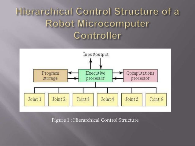
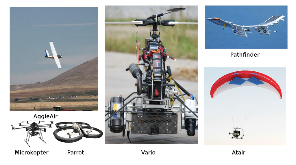
The miniaturization of electronics, computers and sensors has created new opportunities for remote sensing applications.
++++++++++++++++++++++++++++++++++++++++++++++++++++++++++++++++++++++++

+++++++++++++++++++++++++++++++++++++++++++++++++++++++++++++++++++++++++