Ultra-thin chips for high-performance flexible electronics


Flexible electronics has significantly advanced over the last few years, as devices and circuits from nano scale structures to printed thin films have started to appear. Simultaneously, the demand for high-performance electronics has also increased because flexible and compact integrated circuits are needed to obtain fully flexible electronic systems. It is challenging to obtain flexible and compact integrated circuits as the silicon based CMOS electronics, which is currently the industry standard for high-performance, is planar and the brittle nature of silicon makes bend ability difficult. For this reason, the ultra-thin chips from silicon is gaining interest. This review provides an in-depth analysis of various approaches for obtaining ultra-thin chips from rigid silicon wafer. The comprehensive study presented here includes analysis of ultra-thin chips properties such as the electrical, thermal, optical and mechanical properties, stress modelling, and packaging techniques. The underpinning advances in areas such as sensing, computing, data storage, and energy have been discussed along with several emerging applications (e.g., wearable systems, m-Health, smart cities and Internet of Things etc.) they will enable. This paper is targeted to the readers working in the field of integrated circuits on thin and bendable silicon; but it can be of broad interest to everyone working in the field of flexible electronics.
INTRODUCTION

Flexible electronics is changing the way we make and use electronics.
Many existing applications such as implantable systems that require
bend ability to conform to the curved surface of tisues1
are driving the progress in the field, which in turn is the enabler for
numerous futuristic applications such as mHealth, wearable systems,
smart cities, and Internet-of-Things (IoT). Several initiatives from
governments and industry have also contributed to the progress and it is
now estimated that the market for flexible electronics will reach $300
billion by 2028,2,3 with growth from $29.28 billion in 2017 to over $63 billion in 20234
for printed, flexible and organic electronics alone. The
high-performance, at par with today’s complementary metal oxide
semiconductor (CMOS) electronics, will be critical to this growth in
flexible electronics as several current and future electronics would
need fast communication and computation. For example, large drive
currents and fast readout is needed in application such as interactive
flexible displays. Likewise, wireless communication in mHealth or IoT
(where wearable sensors patches are needed for continuous measurements)
will require data handling in frequency bands up to ultra-high
frequencies (0.3 – 3 GHz).5
The faster communication, higher bandwidth, and efficient distributed
computation with very high clock speed will make the high-performance
requirement inevitable in connected objects. This high-performance
requirement calls for investigations into new materials, fabrication
technology, methodologies, and design techniques6—all
of which influence the device performance. For example, the transistor
switching frequency is influenced by the mobility and channel
length—while mobility is a material property, the channel length depends
on the technology. To demonstrate how various materials link to
performance, we have compared in Table 1 some of the materials used in flexible electronics. This comparison is in terms of carrier mobility (µ), channel length (L), transit frequency (f
t
), and the Ion/Ioff
ratio of transistors that use these semiconducting materials as current
channel. Assuming fixed FET parameters such as channel width, oxide
capacitance etc. and the voltages such as terminal and threshold
voltage, the dependency of transit frequency (which is a measure of
transistor speed) boils down to mobility and channel length.
The technology readiness to obtain devices down to nanoscale dimensions
and the possibility to exponentially scale the device densities up to
billions of devices per mm2, makes silicon based
microelectronics a good candidate for addressing immediate
high-performance needs in flexible electronics. For this the first issue
that need to be overcome is the lack of flexibility (and hence
conformability) of silicon wafers. This has been achieved by thinning
the wafers down to <50 µm using a range of technologies, which are
discussed here. Silicon chips from such thinned wafers, or ultra-thin
chips (UTCs), are ideal for high-performance flexible electronics as
they are physically bendable and have stable electronic response for
particular bending state.13
The excellent form factor of UTCs make their integration on flexible
substrates better than the conventional thick chips. Further, due to
reduced package volume and lower parasitic capacitance, the UTCs have
better high-frequency performances and lower power consumption. With
these features UTCs can underpin advances in areas such as sensing,
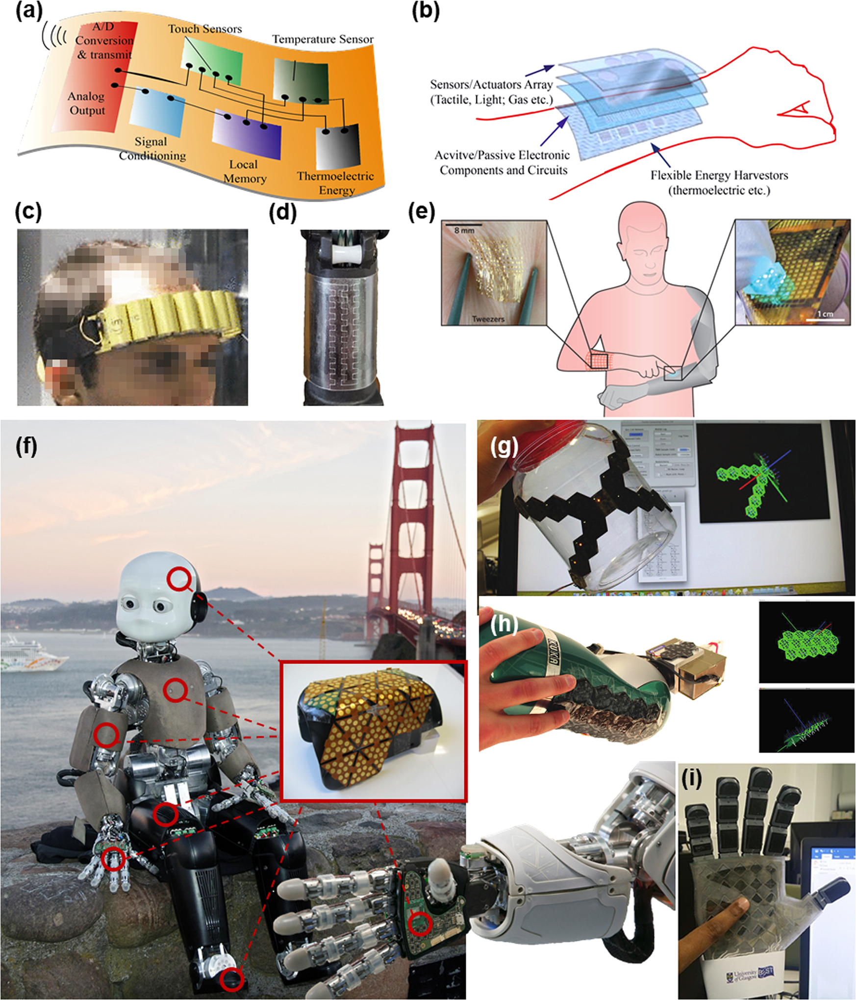
computing, data storage, and energy (Fig. 1)
and several emerging applications (e.g., robotics, wearable systems,
m-Health, smart cities and Internet of Things etc.) they will enable.
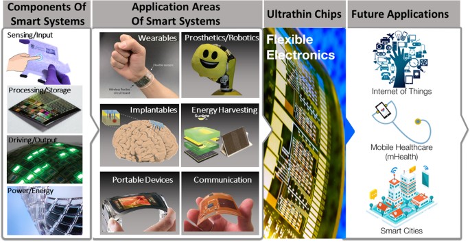
Applications enabled by UTCs through underpinning research in areas such as sensing, computing, data storage, and energy.
Given the wide scope of UTCs, a comprehensive review of various
technological and applied aspects will complement several other reviews
that have mainly focussed on organic semiconductors and their processing
techniques such as printing or vacuum deposition etc. A few review articles have also discussed layer transfer processes and thin film silicon for solar cells.
Related to UTCs, only a few review articles have been published and
they have covered limited areas such as wafer thinning methods such as
back grinding and integration on flexible substrate using stretchable
interconnects.
The analysis of UTCs covering topics such as changes in
electrical-mechanical-optical-thermal properties, packaging, and
stress-induced response variations, and comparison of various thinning
methods has not been reported thus far.
UTC properties
The physical dimensions could influence the material properties and
carrier transport mechanism and therefore could affect the performance
of electronics devices. Compared to their bulk counterparts, the UTCs
exhibit different behavior in terms of mechanical flexibility, optical
transmittance, and carrier surface mobility (e.g., upon experiencing
stress) etc. These variations can be challenging to handle, for example
when one attempts to apply on UTCs the methods and designs developed for
conventional bulk silicon. At the same time, such variations also offer
multiple new opportunities, which are otherwise difficult with bulk
silicon. For example, Si starts to become optically transparent for
thicknesses below 10 µm—starting in the red region and progressing
towards blue region as the wafer gets thinner. Such thinning led
variations in optical transparency of Si could be exploited to improve
photodetectors and solar cells etc., as explained later in this section.
An extensive analysis of variations in properties with respect to
thickness has not been reported and this section should fill the gap in
literature.
Mechanical properties
The thinning process impacts the mechanical properties of thinned electronic substrate. For example, during thinning by back grinding, the sub-surface damage (SSD) and deep cracks in Si result in poor bendability and eventually lead to early breakage of UTCs. Likewise, the etch pits and hillocks produced during thinning by wet etching could lead to localized stress and can decrease the breaking strength of Si. The localised stress or stress distribution at different locations in UTCs are typically studied with Finite Element Analysis and Micro-Raman Spectroscopy. The FEM analysis can provide an estimate of the residual stress at critical position like hinge and centre and the shift in Raman peak could provide deep insight into localised mechanical stresses. The mechanical strength of UTCs is also influenced by their thickness and the stress generated during the bending .Thermal properties
Temperature is known to have significant impact on the performance and reliable operation of electronics and therefore discussion on thermal properties of UTCs gain importance. The heat dissipation, particularly in the UTCs realized from SOI wafers having top Si thickness in the nanoscale, significantly differ from conventional bulk Si based chips. For example, the thermal conductivity of <100 nm Si is half the value of undoped bulk Si (~148 Wm−1 K−1). The lower thermal conductivity means the heat generated is not easily transferred to the package and therefore appropriate heat management may also be needed for UTCs, especially for high-performance flexible electronics. Another important factor is the dependence of mobility on temperature, which is determined by four types of scattering (phonon scattering, surface roughness scattering, bulk charge coulombic scattering, and interface charge coulombic scattering). The net effect of this complex dependence is that higher the temperature, lower is the mobility and therefore increase in the temperature due to low thermal conductivity of UTCs could degrade the system performance. Likewise, the threshold voltage decreases because the metal to semiconductor work function and fermi potential decrease with temperature. The thermal issues can be overcome by incorporating on-chip cooling architecture such as micro-coolers and thermo-electric fluidic cooler. However, this is cumbersome process and will typically require a liquid cooling mechanism. A potential alternative is to use large size UTCs. As an example, with COMSOL simulation . it has been shown that a 1 mm × 1 mm conventional chip (0.5 mm thick) on a 0.5 mm thick polyimide can heat up the substrate to 40 °C even with a small power density of 1 Wcm−2. However, in larger chips, the heat is distributed over larger area and therefore local heating is reduced. Applying the same argument to thin chips (~100 µm thick) on polyimide substrates, with same power but bigger area (10 mm × 10 mm), the simulation result show only 2 °C more temperature than ambient. This much increase in the local temperature is within acceptable limit for applications such as biomedical implants and wearables where higher temperatures can damage tissues. Embedding of air-channels in thin chips could alleviate the issue as it helps in the cooling of the chip. However, such solutions put a restriction on the type of methodology used to develop UTCs.Optical properties
Owing to varying absorption coefficients at different wavelengths, Si starts to become optically transparent as the thickness decreases—starting with the red region and progressing towards blue region.Electrical behaviour
The fundamental electrical properties of Si such as its bandgap, dielectric constant, density of states, will not change until the thickness reaches nanoscale. For most of the flexible electronics applications, the flexibility requirements could be fulfilled with UTCs having thickness in the range of 5–50 µm. Therefore, for practical purposes the fundamental electrical properties of ultra thin Si remains unchanged when they are realized by thinning bulk Si. To reach <50 µm, the thickness of a conventional bulk wafer or SOI wafer undergoes thinning process, which is known to induce stress in Si. The Si chip could also be stressed by various fabrication steps such as deposition of different material layers like oxide, dielectrics, and metal etc., which have different elastic modulus. On top of these, there is additional stress when the UTCs are externally loaded or strained, for example, during bending. Whereas the thinning and process induced stress are intrinsic to chip, the bending induced stress during usage is external. These stresses induce changes in the band structure and the piezoresistive property of Si, which eventually show up as variation in the electrical response of devices on UTCs. Through electromechanical tests and modelling, a few works have attempted to capture the stress induced changes in electrical response of devices. For example, in the case of uniaxial bending, n-type MOSFETs show increase in mobility with increase in bending stress. In n-type MOSFETs, this behaviour is independent of the direction of bending, but variations in the response of p-type MOSFETs is direction dependent. The models in these works have taken into account the process strategies, dimensions of the structure (active Si, dielectric, metal thicknesses, etc.), initial substrate (e.g., Si, SOI, UTSOI, ETSOI etc.), mechanical strain etc. The stressed induced changes could lead to significant deviations in the response of device and circuits from their specified value , where bending induced changes in device and circuit parameters are reported. For complex circuit design in flexible electronics and to predict their response under different bending condition precisely, it is necessary to understand these variations and implement predictive models in electronics design tools. The variations in device response could be reduced by using suitable compensation techniques in the layout. On other hand, these changes in the device parameters could also be seen as the signature for a particular bending state and therefore could be used to predict or sense the state/shape of bending.Technologies for realizing UTC
A wide range of technologies have been explored for realizing UTCs . For the sake of completeness, the technologies involving either bulk Si wafer or SOI wafer are briefly discussed in this section. Figure 4 also gives a summary of these technologies, classified based on the fabrication stage at which the thinning is carried out. For example, when the thinning is carried out after the fabrication of electronic devices it is termed as post-processing, and when wafer undergoes some processing before the device fabrication then it is termed as pre-processing. Generally, the thinning is carried out after the device fabrication is completed. the choice of technological approach to realize UTC requires careful consideration.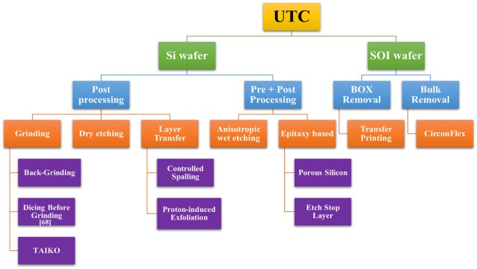
Classification of various thinning methodologies for realizing UTC
Using Si Wafer
UTC via post-processing techniques
In post-processing approaches, the UTCs are typically obtained by physical removal of electronic substrate such as Si through either grinding, dry etching, chemical reaction or combination of these. In these techniques, the crystal structure of active Si area (for example, in the case of MOSFETs, the area up to well-depth) is unaffected and therefore their electrical response is at par with their bulk counterparts. However, as discussed in previous section the possibility of mechanical degradation cannot be ruled out. The techniques used as post-processing step can be broadly divided into: (i) grinding, (ii) dry etching, and (iii) layer transfer.Grinding
Back grinding is a popular and well established method for wafer thinning. The protective tape, which holds the wafer to chuck during grinding, plays a significant role in determining the total thickness variation (TTV) as the wafer gets thinner. Wafers with thickness as low as 3 µm have been obtained with this technique. Back grinding is faster with respect to other techniques, but it is also known to damage the crystal structure deep inside the material. The sub surface damage could induce high stress in the thinned wafer and can cause thin wafer or UTCs to warp. This type of stress concentration can also lead to breakage during handling, for example, while removing the thin wafer from chuck or during dicing of thin wafer. Therefore, stress-relieving techniques such as slow ion etching and chemical-mechanical polishing are recommended after back grinding. Dicing before grinding (DBG) is also sometime used to prevent breakage of thinned wafers during dicing. In DBG, the wafers are first partially-grooved and then grinded .occurring when the wafer is thinned below the level of this cut. A major problem with grinding is that there is high potential for the thin wafer getting damaged while it is being delaminated from the protection tape. This issues could be overcome by TAIKO technique in which back-grinding is done only for non-peripheral part of the rear side of wafer and the periphery is left intact as a ring . The ring-shaped periphery strengthens the overall structure and significantly reduces the issue of warpage during handling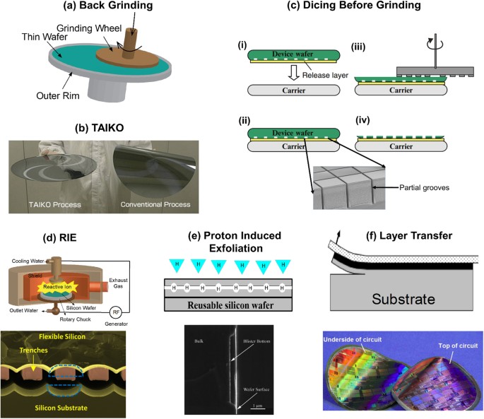
A Illustration of Back Grinding. b TAIKO wafer vs. conventionally thinned wafer. c Steps involved in Dicing Before Grinding . d Illustration of RIE and SEM image of trenches etched between released top layer and bulk substrate. e Proton-Induced Exfoliation technique and blister created after heating hydrogen implanted wafer. f Illustration of controlled spalling and flexible wafer over polyimide .
Dry etching
Physical dislodging of Si atoms from the bulk could also be achieved with high-energy ions and gaseous reactive species. Depending on the mechanism, the process can be classified as: (i) physical ion etching (PIE), and (ii) reactive ion etching (RIE). In PIE, the atoms from the back of the substrate are removed by bombarding it with energetic ions or gas assisted etching. The etch rate depends on parameters such as scanning style, substrate chuck table angle, beam angle etc. There is always some re-deposition in this process, which reduces the effective etch rate and selectivity. In the case of RIE, the high-energy ions impacting the substrate remove the atoms physically and open-up the area for chemical reaction as illustrated in Figure . RIE gives high anisotropic behaviour but it comes with low level of selectivity (in absence of any additive) and surface damage. A few examples of RIE based UTCs include a 18 µm thick Si based thermoelectric energy generators and Si probes of thickness 20 µm for floating chronic implantation in the cortex.Layer transfer processes
This method involves removal or exfoliation of the top processed layer. Two major processes developed based on this technique are: (i) proton-induced exfoliation and (ii) controlled spalling. In the case of proton-induced exfoliation, wafer is placed in a vacuum chamber after device fabrication and exposed to a beam of hydrogen ions. When heated, these ions which were implanted beneath the surface, expand as microscopic hydrogen bubbles—thus causing a very thin Si layer to detach from the surface, as shown in Figure. The wafer can be reused to exfoliate another layer of ultra-thin Si. However, this method is not suitable for post-processing as electronic devices may be damaged because of high-energy proton exposure. Another layer transfer process is the controlled spalling technique, which takes advantage of strained conditions to obtain thin Si layer. Under specific strain conditions, a fracture on the edge of a brittle substrate can propagate parallel to the surface, as shown in Figure . This results in the detachment of thin slice of the brittle. This process can be carried out at room temperature and therefore it has advantages in terms of integration on flexible substrates. The techniques has been demonstrated with nanoscale flexible circuits (functional ring oscillators and memory cells) on 60 Å thick ultra thin Si over the oxide of SOI. One of the challenges with controlled spalling is that it requires pre-calculation and monitoring of stress level to minimize the spontaneous fracture. This can be overcome with appropriate material and thickness of top film used as stress layer.UTC via pre-processing techniques
Some technologies for UTCs require processing of wafers before initiating the device fabrication. These steps are termed as pre-processing steps and the front-end fabrication follows thereafter. The techniques for realizing UTCs which require pre-processing are discussed below:Anisotropic wet etching
This well-established technology has been used traditionally to realize MEMS (microelectromechanical systems) structures. The pre-processing steps for realizing UTCs involve depositing suitable mask layers (usually a combination of high quality SiO2 and Si3N4) at defined locations on the back side of the wafer . This is followed by the device-processing steps on the front-side, and then etching of wafer from backside. The commonly used etchants for Si are hydrazine, EDP (Ethylene-Diamine-Pyrocatechol), TMAH (Tetra methyl ammonium hydroxide), and KOH (potassium hydroxide). The etching duration can be in hours depending on the concentration of etchant, the temperature and thickness of the wafer. The contamination from etchant and their CMOS compatibility is an important requirement, among others including modulating etching with dopants or electrical bias, surface roughness, availability of suitable masking films, health hazards, and disposal issues. TMAH is the most commonly used etchant as it is IC-compatible, nontoxic, and has very good anisotropic etching characteristics. One drawback with TMAH is that it leads to higher undercutting than other etchants such as KOH. To overcome this issue the isopropyl alcohol (IPA) and surfactants are generally added to TMAH. The wet etching can provide thin wafers at batch scale since many wafers can be processed at once. The wafer scale UTCs with TMAH etching and transfer to flexible substrate has been reported in literature. The protection of front-side of the wafer from etchant is a critical for this route to obtain UTCs as otherwise the etchant may render the devices on the front side useless. To provide front-side protection, a custom wafer holder made from etchant resistant material or polymeric protection layer are used. The concentration of etchant is maintained regularly during this process to have better control over the total etch time leading to UTCs with desired thickness. A potential solution for monitoring the etch process is to exploit the change in optical transmittance with thickness, as discussed in the section “Ultra-thin chip properties”.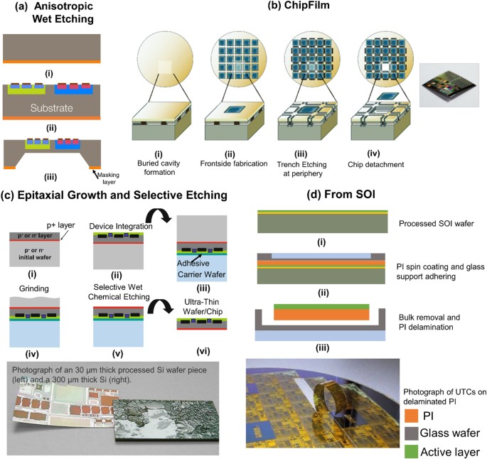
Illustration of pre-processing and post-processing modules of a Wet Etching, b ChipFilm, c various steps in epitaxial growth and selective etching approach and d CirconFlex technique using SOI wafer.
Epitaxial Si based UTCs
The UTCs with devices having higher operating speed and better bipolar performance can be obtained by lifting-off Si epitaxial layer from the substrate. The two key approaches used for this purpose are: (a) Porous Si Approach, and (b) Etch Stop Layer Approach. The porous Si method, developed in 1990s, involves creation of a porous layer between substrate and the epitaxial layer. Examples for this approach included the ChipFilm technology , which uses two layers of porous Si with different porosity and results in ~15 µm thick UTCs. This technology allows good dimensional control and the mother wafer can be used repeatedly until exhausted. The yield of this technology heavily depends on the design and pitch of pillars in porous structure and hence the pre-processing step is critical. While this method is well suited for die-size UTCs needed in 3D ICs, the large area UTCs may not be practical due to cost considerations and risk of breaking due to warpage. One possible solution to address this issue is to use double transfer technique (i.e., using flexible carrier and substrate) instead of pick-place tool.The etch stop layer method, typically used in a MEMS, takes advantage of the fact that doping could be used to stop etching. It involves developing a highly doped (p++ type) film at certain depth (roughly equal to desired thickness of UTCs) on the front side of wafer, followed by lightly doped epitaxial layer which act as active layer for device fabrication. Post device fabrication the wafer is chemically etched from back side until the chemical hits the p++ layer, which stops the etch process. The final thickness of UTC is the equivalent to the thicknesses of the epitaxial and p++ layer. With a good control over the final thickness and uniformity of UTCs, this method . offers an alternative solution to the SOI wafer based approach. During growth process, the diffusion of impurities between Si wafer and p++ film may prevent the fabrication of an ideal step junction, which may lead to lower switching current ratio and hence the poor performance of electronics on UTCs. One way to control the impurity diffusion is to adopt low temperature epitaxial growth with a trade-off between high quality epitaxial film and higher impurity diffusion.
Using SOI wafer
SOI wafers provide a range of benefits relative to conventional wafer, such as, lower parasitic capacitance, resistance to latch up, lower leakage current, and immunity to radiation induced soft errors. While these features of SOI wafers enable high-performance electronics, their higher cost (~$1000 vs. ~$25 for a 6-inch bulk Si wafer) is a barrier. Nonetheless, despite this cost-performance trade-off, the SOI wafers are used in many niche applications such as low power high performance RF chipsand commercial devices such as IBM’s PowerPC,Global Foundry’s 22FDX, AMD’s dual core module. SOI wafer could also be used for high performance UTCs with precise thickness. This is achieved by fabricating electronic devices on the top active layer of SOI wafer, followed either by: (a) etching the buried oxide layer (i.e., BOX removal), or (b) thinning the backside of the wafer up to the required thickness or buried oxide (i.e., bulk removal) in which case the oxide acts as the etch stop layer.BOX removal
In this method, the trenches are etched around the chip on the front side and then etchant such as HF or XeF2 is passed through these trenches to etch the oxide layer underneath, eventually detaching the top chip from the mother wafer. Since the trench formation is critical, the area available for device realization is limited and therefore well laid out design scheme is needed. Moreover, it calls for proper support of top Si layer as soon as it is detached from the bulk. Such challenges can be overcome through transfer printing using PDMS or similar intermediate carrier. Transfer printing of UTC based devices such as transistors, logic gates, RF components has been demonstrated for numerous applications.Bulk removal
In this process, the bulk Si is removed from backside by wet etching until the etchant reaches the buried oxide. In this case, the buried oxide acts as the etch stop layer and UTC thickness is sum of active layer and BOX thicknesses. A variant of this technique developed by Philips is named as Circonflex. Based on substrate transfer technology, this process enables the transfer of top functional layer of SOI wafer to practically any flexible substrate . The method has been demonstrated for realizing 10 µm thick RF-ID tag chipsIntegration of UTCs on flexible substrates
For fully flexible systems with reliable operation, the UTCs need to be
packaged over flexible substrates, sometimes with more than one chip on
the same substrate. The choice of substrate is critical and depends on
the inherent material properties and the intended application. The
materials which have been used as flexible substrate can be broadly
divided into two categories, i.e., polymeric and metallic .
An insulation coating is generally needed for electrical isolation of
UTCs and to connect them to various components on flexible substrate and
external connections. However, there are some exceptions such as solar
cells where the required common back contact is achieved by transferring
UTSi (Ultra-Thin Si) on flexible metallic or conductive-material-coated
polymeric substrates.
The metallic substrates for flexible electronics have an added
advantage as they can serve as heat sink or means for thermal reliefs.
Further, they can be useful in applications such as electrical wave guide
or where electromagnetic shielding is required. This can also be
achieved with polymeric substrates coated with a thin conductive
material including metals .
However, metallic substrates have inherent tendency towards retaining
the shape on deformation, which may not be desirable. In this regard,
thin polymeric substrates are advantageous as they are inherently
elastic and flexible with ability to regain their normal shape. An
alternative approach is to use a stack of both polymeric and metallic
substrates and engineer the structure to realize smart substrates with
desired properties. Thermal properties of substrate such as coefficient
of thermal expansion and thermal conductivity should also be considered
as they influence integration and thermal management of UTCs. As the
stress level in UTCs is influenced by elastic properties of the
substrate, generally a material with lower Young’s Modulus is preferred.
With the increasing interest in health or bio related applications such
as implantable systems, bio-compatibility of substrate is also an
important parameter to consider. Bacterial cellulose membrane, collagen,
silicone gel and silk fibroin etc. have been used in such applications
as they also offer better integration with tissues.
The most challenging task in the packaging of UTCs comes when the contact pads on the chip are to be connected to the extended pads on the substrates. Wire bonding technique, which is widely used for traditional packaging is not suitable for UTCs, which are fragile and can crack due to the impact of bonding head-tool. Further, the bond wires protruding out of plane of UTCs add to the thickness and affect the form factor. These challenges are driving the search for suitable materials and techniques for UTC packaging. The integration of UTCs on flexible substrate have been achieved mainly by the following three techniques.
Flip chip assembly on flexible substrate
In this style of packaging, UTCs in face down configuration are assembled on polyimide or liquid crystal polymer (LCP) substrate through flip chip bonder . In the case of polyimide substrate, the solder bumped die are reflow soldered to the patterned flex. In the case of LCP, vias are etched through to expose the underside of contact pads. However, these solder bumps become coarse due to ageing and the growth of intermetallic compound, which eventually results in a changing shear mode and increase of resistance. A right combination of temperature and pressure at the curing step is needed during flip chip technique to get reliable electrical joints from bumps. The major limitation of flip chip techniques is seen in the case of packaging of sensors requiring their sensing area to be exposed, as in the case of POSFET (Piezoelectric oxide semiconductor field effect transistor), ISFET (ion sensitive field effect transistor) etc.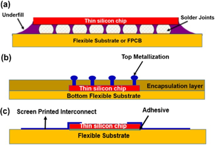
Major schemes of packaging UTC: a Flip-Chip packaging of UTC, b UTC lamination between two flexible layers and c UTC on flexible substrate with screen-printed connection
Laminating UTCs between two flexible layers
This type of packaging generally aims to put UTCs in the neutral plane by embedding it between the substrate and encapsulation layer . The advantage of this approach is that it leads to a reduced stress on UTCs and as a result the electrical response of UTC is minimally affected by bending. The integration of UTCs between two polyimide layers has been demonstrated for conformable and wearable wireless ECG monitoring system. A challenge with this type of packaging is that the heat produced during device operation cannot escape to ambient. This could lead to high local temperature and can damage or degrade the device performance, as also discussed in the section “Ultra-thin chip properties”. Moreover, the adhesion between the polyimide and the Si may vary due to localized area of high temperatures and this could lead to uneven adhesion of package or air bubbles formation within the package. In this direction, the on-chip cooling mechanism could be explored. For example, the nanostructured super lattice-based thin-film thermoelectric material (e.g., Be2Te3) integrated with Si based electronics results in reduction of temperature by ~14.9 °C at target site. Similar advances could be explored for UTCs to improve the reliability of package. Recently, embedding of micro-air vertical channels in UTCs have been reported for faster cooling and lower constant load saturation temperature. Use of flexible materials with high thermal conductivity (e.g., copper, graphene, etc.) and structuring them as fins to act as a heat sink or using commercial thermal conductive tape outside the package are other potential solution.UTCs on foil with printed connections
In this approach, UTC are placed in the face-up configuration on the flexible substrate using epoxy based adhesive. Conductive wires are printed-on top of flexible substrate to realize electrical connections between the chip and the substrate . Screen printing or ink-jet printing is used to connect the contact pads on chip to the external connections on the flexible substrate. Silver based conductive ink and polymer based conductive material like Poly (3,4-ethylenedioxythiophene): polystyrene sulfonate (PEDOT:PSS) have been used for this purpose. The silver ink provides much higher conductivity than PEDOT:PSS but it is susceptible to cracking during bending. On other hand, PEDOT:PSS provides more flexibility than silver ink but shows low conductivity. A durable connection by combining screen printed silver grid with PEDOT:PSS could be a potential solution. Although printing is simple and can be extended to large area, due to poor resolution of printers the contact pads and wires realized through printing are usually big in comparison to contact pads on the chip. This issue will be overcome with advances in printing technologies.For fully flexible electronics system other materials may also be used in conjunction with UTCs. For example a:Si/Poly-Si, inkjet or transfer printed nanowires, 3,3‴-didodecylquarterthiophene (PQT), solution processed organic/inorganic materials such as peri-xanthenoxanthene (PXX), Lithium Super Ionic CONductor (LISICON), pentacene, dinaphthothienothiophene (DNTT), copper hexadecafluorophthalocyanine (F16CuPc), PEDOT, and thixotropy materials, etc. could be used to obtain advanced multifunctional flexible electronics systems.
Energy autonomous electronic skin
Design UTC in e- S H I N to A/ D / S Tour Route
Applications of UTCs
A
wide range of applications require UTCs as through underpinning
high-performance electronics they enable advances in several areas, as
illustrated in Fig. 1.
The UTCs form the key components of various smart systems as sensing
units, data processing or storage unit, driving or output unit and power
or energy management units etc. Depending on the application
requirements, the specification of electronics/sensing components on
UTCs may vary. Some of the applications where UTCs are used as sensing
units, data processing or storage unit, driving or output unit, and
power or energy management units are described below.
In order to achieve biomimetic tactile sensing, about 250 MRs/cm2 are required in the fingertip of prosthetic limb, which could be achieved by high density tactile sensors such as flexible POSFET that can conform to fingertips.Further, UTCs could be useful for large area tactile skin based on planar off-the-shelf electronics integrated on FPCBs. Lack of bendability of electronics has often limited the use of large area skin to body parts with large curvature. UTCs are ideal to address such applications as besides high-performance sensing they could also conform to the curved surface of prosthesis.
Implantable systems have brought a distinctive transformation in the field of medical diagnosis and treatments. Flexible microchips with integrated sensors or microelectrodes are advantageous for applications such as brain interfaces as they can conform to soft tissues and hence allow recording of reliable data. Flexible UTCs with RFIDs encapsulated with biocompatible liquid crystal polymers has been successfully implanted and tested. UTCs also find application in video endoscopy, smart catheters, diagnostic pills, sub-retinal implants, neural interfaces,swallowable smart pill and tactile functional prosthetics etc. In the field of medical diagnosis, UTCs find application as conformal retinal implant for blind vision, electromyographic and/or neural prosthetic implant, and blast sensor patch in sports/military helmets to detect trauma injury. Neurotechnology is another area which will greatly benefit from electronics that bends, stretches and conforms to curved surfaces. For example, complementing current in vivo studies, the flexible and conformal microelectrode arrays will offer powerful new tool in traumatic brain injury research. UTCs are attractive for such applications as in addition to the active microelectrodes they could also offer functionalities such as wireless communication. Thanks to the flexibility and conformability, the UTCs will be far more comfortable for people using them.
In applications for health monitoring where the devices are worn or wrapped around the body the high-performance and compact electronics on UTCs could provide solutions such as measuring human pulses on wrist, and orthodontic forces of invisible aligners for dental treatment. The convergence of soft and deformable textiles technologies with high-speed computational capacity of UTCs is another application. The rough and uneven surface of fabric makes it difficult to have seamless integration of UTC, which could be solved by using smoother intermediate layer between textile and UTC. The UTCs can have sensors, interconnects and processor for on-chip processing of the data. This type of arrangement will greatly influence the applications such as military garment devices, antibacterial textiles, and personal electronics like MP3 jacket and smart carpet.
Flexible portable devices, smart contact lenses or augmented reality systems are some other areas where UTCs could trigger advances as they could enable high-speed computation at lower power and high-density storage. The Ferroelectric Random Access Memory (FeRAM) based on flexible silicon shows superior performance and can be good choice for flexible memory applications for IoT. Emerging memory devices such as RRAM (Resistive random-access memory), memristors, and other high density nanoelectronic non-volatile memories could also be integrated with UTC technology.
In applications such as bidirectional prosthesis at par with human hand, the electronics on e-skin should process data from 18k mechanoreceptors (MRs) to mimic the glabrous palm area of a hand. As number of sensory components increase, there is demand to handle large data. The on-site processing and signal conditioning of the raw data can be fulfilled by UTCs integrated on the e-skin. While the active tactile layer could comprise of large area flexible material such as graphene, the sensory data from array of taxels should be processed locally by a tactile interface IC before it is fed into the computing chip. The high-performance UTC serve are ideal for such task. They could also reduce the load on the computing block or could enable new features such as multitouch input, 2D and 3D gestures, handwriting recognition, pen/stylus input, pressure sensitivity, fingerprint recognition, and security operations. In areas such as wearable systems, where different modules need to communicate within and outside the system, the UTCs could be used to develop components for body area networks, and RF communication such as Bluetooth 4.0 low energy communication etc.
In applications such as smart portable display, there is a growing interest in manufacturing portable devices with flexible display that can undergo bending, flexing and rolling. While flexible AMOLED display are commercially available, for flexible smartphone various components such as battery, driving unit, communication chip etc. are not bendable yet. Some of these form the areas of active research, for example, flexible batteries. With high performance flexible circuits, UTC could remove the current bottlenecks for flexible displays.
Thus, with several applications, the UTCs could bridge the gap between CMOS technology and several of the above mentioned emerging applications of flexible electronics.
Sensing/input
UTCs smart sensing units offer interesting solution for several existing applications such as implantable systems, neurotechnology, wearables, robotics and prosthetics etc. Futuristic applications such as body area network, body-dust, neural interfaces, bidirectional prosthesis, internet of everything and smart homes etc. will also benefit from UTCs based sensing units. As tactile interface chip for flexible touch panel, the UTCs will bring transformation in flexible portable devices and e-skin for prosthesis or robotics (a flexible and transparent electronic skin as illustration for sensing/input in Portable devices such as smartphones are expected to be flexible in the future, and for this to happen various components including touch panel should be flexible. In such cases, the active tactile layer could comprise of large area flexible material such as graphene, but the sensory data from array of taxels will be processed locally by a tactile interface IC or neuromorphic ICs before the data is transferred to complex computing hardware. UTCs will strengthen the capability of such systems by enabling features that require high-performance such as multitouch sensing, 2D/3D gestures, handwriting recognition, pen/stylus input, pressure sensitivity, fingerprint recognition, and security operations.In order to achieve biomimetic tactile sensing, about 250 MRs/cm2 are required in the fingertip of prosthetic limb, which could be achieved by high density tactile sensors such as flexible POSFET that can conform to fingertips.Further, UTCs could be useful for large area tactile skin based on planar off-the-shelf electronics integrated on FPCBs. Lack of bendability of electronics has often limited the use of large area skin to body parts with large curvature. UTCs are ideal to address such applications as besides high-performance sensing they could also conform to the curved surface of prosthesis.
Implantable systems have brought a distinctive transformation in the field of medical diagnosis and treatments. Flexible microchips with integrated sensors or microelectrodes are advantageous for applications such as brain interfaces as they can conform to soft tissues and hence allow recording of reliable data. Flexible UTCs with RFIDs encapsulated with biocompatible liquid crystal polymers has been successfully implanted and tested. UTCs also find application in video endoscopy, smart catheters, diagnostic pills, sub-retinal implants, neural interfaces,swallowable smart pill and tactile functional prosthetics etc. In the field of medical diagnosis, UTCs find application as conformal retinal implant for blind vision, electromyographic and/or neural prosthetic implant, and blast sensor patch in sports/military helmets to detect trauma injury. Neurotechnology is another area which will greatly benefit from electronics that bends, stretches and conforms to curved surfaces. For example, complementing current in vivo studies, the flexible and conformal microelectrode arrays will offer powerful new tool in traumatic brain injury research. UTCs are attractive for such applications as in addition to the active microelectrodes they could also offer functionalities such as wireless communication. Thanks to the flexibility and conformability, the UTCs will be far more comfortable for people using them.
In applications for health monitoring where the devices are worn or wrapped around the body the high-performance and compact electronics on UTCs could provide solutions such as measuring human pulses on wrist, and orthodontic forces of invisible aligners for dental treatment. The convergence of soft and deformable textiles technologies with high-speed computational capacity of UTCs is another application. The rough and uneven surface of fabric makes it difficult to have seamless integration of UTC, which could be solved by using smoother intermediate layer between textile and UTC. The UTCs can have sensors, interconnects and processor for on-chip processing of the data. This type of arrangement will greatly influence the applications such as military garment devices, antibacterial textiles, and personal electronics like MP3 jacket and smart carpet.
Data processing/storage
The consumer electronic devices such as smart phones, mobile gaming systems, and ultrabook computers etc. have fueled the growth of semiconductor industry in recent years. Consumer prefer smaller, thinner, and lighter systems with additional features such as wearable to meet their mobile lifestyles. Thanks to Moore’s law and ITRS roadmaps, CMOS technology has come a long way breaking many challenges with many material and technology innovation leading to the current state-of-the-art. Commercially, 14 nm technology FinFET based microprocessors are available which operates at >4 GHz and now gearing to 10 nm. Considering the huge number of objects, with different size, shape and rigidity, which will be connected in IoT environment, high performance, and mechanical flexibility of devices employed in these objects is inevitable. As discussed in the section “Introduction”, the wireless communication in IoT will require data handling ultra-high frequency range. UTCs will be useful here as they could support faster communication, high bandwidth, and efficient distributed computation with very high switching speed. With interconnect schemes such as through-silicon-vias, low power consumption and excellent high performance, the UTCs have potential for 3D integrated circuits (3D ICs) to handle large amount of data and processing in IoT concept.Flexible portable devices, smart contact lenses or augmented reality systems are some other areas where UTCs could trigger advances as they could enable high-speed computation at lower power and high-density storage. The Ferroelectric Random Access Memory (FeRAM) based on flexible silicon shows superior performance and can be good choice for flexible memory applications for IoT. Emerging memory devices such as RRAM (Resistive random-access memory), memristors, and other high density nanoelectronic non-volatile memories could also be integrated with UTC technology.
In applications such as bidirectional prosthesis at par with human hand, the electronics on e-skin should process data from 18k mechanoreceptors (MRs) to mimic the glabrous palm area of a hand. As number of sensory components increase, there is demand to handle large data. The on-site processing and signal conditioning of the raw data can be fulfilled by UTCs integrated on the e-skin. While the active tactile layer could comprise of large area flexible material such as graphene, the sensory data from array of taxels should be processed locally by a tactile interface IC before it is fed into the computing chip. The high-performance UTC serve are ideal for such task. They could also reduce the load on the computing block or could enable new features such as multitouch input, 2D and 3D gestures, handwriting recognition, pen/stylus input, pressure sensitivity, fingerprint recognition, and security operations. In areas such as wearable systems, where different modules need to communicate within and outside the system, the UTCs could be used to develop components for body area networks, and RF communication such as Bluetooth 4.0 low energy communication etc.
Driving/output
The UTCs could also offer solution for efficient driving or output unit for many applications such as optogenetics, flexible portable devices, antenna, actuators. The drive units should provide precise control on current and/or power and/or voltage and/or timing. As an example, in optogenetics pulses of light with spatiotemporal precision are needed to stimulate the neurons and UTCs could be used to achieve this. Typically, optogenetic stimulation is carried out by external light source with fiber-optics to deliver the light to the targeted location. Typical driving requirements is such application are precise temporal requirement i.e., rise time and fall time (10–90% and vice-versa) of current pulses <100 µs and in some specific applications <1 µs and current level up to 1.5 A. Such an arrangement is cumbersome and involves tether. Tether-free implantable miniaturized optogenetic systems are preferred in such cases and UTCs based drivers could provide the required temporal and spatial resolution. Further, with UTCs it will be possible to achieve multi-wavelength and multi-array microLEDs (µLED) targeting various optogenetic channels (corresponding to various opsins) such as channelrhodopsin, halorhodopsin, archaerhodopsin,bacteriorhodopsin. The typical current requirement for such µLED driving is 2–5 mA. Depending on the requirements, the compound semiconductor layers for µLEDs could also be grown or transfer printed on Si, from which UTC is fabricated. Such implantable optogenetic chips can communicate with external transceivers through RF communication in which case UTCs could drive the antennas. Similarly the UTCs could provide the drive/output unit in bidirectional prosthesis, treatments for epilepsy, cardio-arrhythmias, drug addiction, and brain/neural circuit mapping. UTC could also find application in driving flexible pacemakers and defibrillators. For example, the UTC chips integrated with EMG sensing electrodes could process the signal in real-time to identify potential arrhythmia. Wherever needed, they could drive the electrodes to provide stimulus for pacing, cardioversion or defibrillation. UTCs could also drive various components in wearable systems such as LED drivers for pulse oximetry, electro-tactile stimulation, haptic communication gloves for deaf-blind, bendable oral systems (for example to control prosthesis or wheelchair,) smart insole for health monitoring and prosthesis control.In applications such as smart portable display, there is a growing interest in manufacturing portable devices with flexible display that can undergo bending, flexing and rolling. While flexible AMOLED display are commercially available, for flexible smartphone various components such as battery, driving unit, communication chip etc. are not bendable yet. Some of these form the areas of active research, for example, flexible batteries. With high performance flexible circuits, UTC could remove the current bottlenecks for flexible displays.
Power management and energy harvesting
Optimizing battery life for portable systems presents a significant engineering challenge for system designers. While low power high efficiency FETs help in achieving this goal to some extent, alternative approaches are being explored by researchers to harvest energy to develop energy autonomy. Current solutions such as batteries require charging at regular intervals. However, for applications such as health monitoring devices it is advantageous to power the device with energy harvested from the ambient, such as light, heat or motion. UTSi and UTC technology could help in addressing the need for power management and energy harvesting using high efficient flexible solar cells, buck or boost DC-to-DC convertors, power electronics drivers. Photovoltaic technology is one area where thin Si was initially used as explained in the section “Historical perspective”. Due to continuous growth rate over the last decade, the cumulative installed capacity of photovoltaics have exceeded 303 GW-peak by the end of 2016. Monocrystalline silicon based PV with their long life span (up to 40 years) and high conversion efficiency (15–26%) is a better choice. However, the higher cost of monocrystalline silicon (compared to amorphous or micro-crystalline silicon) makes it expensive. In this scenario, UTCs present an interesting avenue. The solar grade large wafers (>8” diameter) are best choice for manufacturing solar panels with ultra-thin Si as active material. However, with lesser thickness the special optical trapping techniques are required to harvest maximum light energy as explained in the section “Ultra-thin chip properties”. The energy harvesting component shows array of micro photovoltaic cells made of monocrystalline Si. Further, a graphene based transparent coplanar capacitive touch sensor combined with solar cells forming a smart energy autonomous electronic skin system . Thermal energy harvesting is another possibility, where a flexible harvester realized on the top of thin Si has been reported to produce around 30% more output power than that of realized on bulk Si.Thus, with several applications, the UTCs could bridge the gap between CMOS technology and several of the above mentioned emerging applications of flexible electronics.
Area Working
The international roadmap for semiconductors (ITRS) highlighted the need for thin chips almost 15 years ago in context with 3D IC staking for system-in-package. In fact, the 2005 ITRS report laid emphasis on UTCs thinner than 20 μm as well as wafer thinning and handling, small and thin die assembly and packaging of thin chips. Until few years ago the demand for UTCs was primarily for 3D system integration, where multiple active dies having active and lateral interconnects are vertically connected through silicon vias. However, this is changing with emerging applications such as mHealth, wearable systems, smart cities, and IoT. The high-performance and flexibility of electronics needed in these applications are primarily pushing the interest in UTCs. In fact, these requirements have fuelled the research for high-mobility materials such as graphene, which owing to excellent electrical, mechanical and optical properties holds the promise for high-performance flexible electronics. However, the technology for these new high-mobility materials is not mature yet for large-scale integration. The limited success of electronics from these high-mobility materials and well-established Si based high-performance electronics respectively act as the push and pull factors of UTC research. A range of silicon based non-bendable devices are already being used in ad hoc arrangements in a wide ranging applications. With this background, this review article has presented and compared the ways to make bendable Si and variations in the response of devices on UTCs because of changes in electrical, optical and mechanical behaviour. Tremendous progress has been made for obtaining UTCs and a range of thinning methods.Going forward, the major hurdles for UTCs will be in the areas related to packaging, modelling and dealing with the effect of stress and strain on electrical response of UTCs. The handling of thin fragile wafers and packaging of UTCs needs more attention. Unlike conventional chips, UTCs cannot be bonded easily with wire-bonder because of high chances of cracks when the bonder tip hits the bonding pad. Reliable and durable connection from chip to the substrate is a challenging task because of the bumps coarsening (in the case of flip-chip bonding) and chances of electrical discontinuity (in the case of screen-printing). With suitable thermal management and embedding the chip between two layers of pre-patterned electrical connection it is possible to overcome the bonding related issues. While much has been done to realize UTCs, the stress induced effects and related models are scarcely researched. A major reason behind the success of Si technology was the availability of accurate models to predict device response. However, this is challenging in the case of UTCs as they experience stress because of external bending. The modelling and simulation of devices on UTCs has not received sufficient attention and this will pose major challenge to the circuit designers. The cost of fabrication of UTCs is also argued as an area that requires attention, especially when they are realized from SOI wafer. However, with mass manufacturing of UTCs the costs will come down and this is likely to be a non-issue. In conclusion, despite many challenges the UTCs hold great promise for advances in many areas where high-performance flexible or conformable electronics are needed.
________________________________________________________________________________
The development of flexible integrated circuits based on thin-film transistors
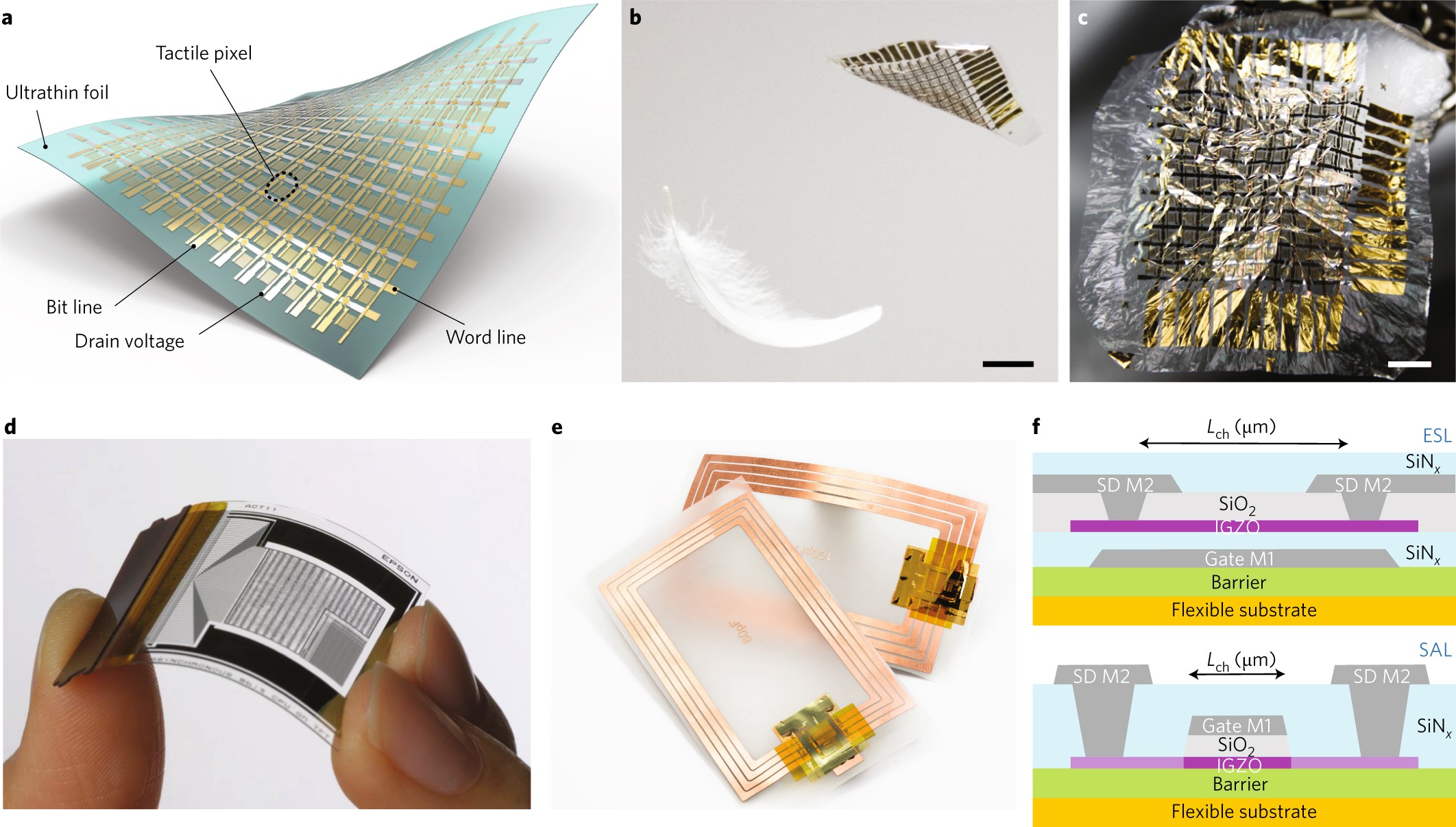
The use of thin-film transistors in liquid-crystal display applications
was commercialized about 30 years ago. The key advantages of thin-film
transistor technologies compared with traditional silicon complementary
metal–oxide–semiconductor(CMOS) transistors are their ability to be
manufactured on large substrates at low-cost per unit area and at low
processing temperatures, which allows them to be directly integrated
onto a variety of flexible substrates. Here, I discuss the potential of
thin-film transistor technologies in the development of low-cost,
flexible integrated circuits for applications beyond flat-panel
displays, including the Internet of Things and lightweight wearable
electronics. Focusing on the relatively mature thin-film transistor
technologies that are available in semiconductor fabrication plants
today, the different technologies are evaluated in terms of their
potential circuit applications and the implications they will have in
the design of integrated circuits, from basic logic gates to more
complex digital and analogue systems. I also discuss microprocessors and
non-silicon, near-field communication tags that can communicate with
smartphones, and I propose the concept of a Moore’s law for flexible
electronics.
_________________________________________________________________________________
Energy autonomous electronic skin
Energy autonomy is key to the next generation portable and wearable
systems for several applications. Among these, the electronic-skin or e-skin
is currently a matter of intensive investigations due to its wider
applicability in areas, ranging from robotics to digital health, fashion
and internet of things (IoT). The high density of multiple types of
electronic components (e.g. sensors, actuators, electronics, etc.)
required in e-skin, and the need to power them without adding
heavy batteries, have fuelled the development of compact flexible energy
systems to realize self-powered or energy-autonomous e-skin. The
compact and wearable energy systems consisting of energy harvesters,
energy storage devices, low-power electronics and efficient/wireless
power transfer-based technologies, are expected to revolutionize the
market for wearable systems and in particular for e-skin. This paper reviews the development in the field of self-powered e-skin,
particularly focussing on the available energy-harvesting technologies,
high capacity energy storage devices, and high efficiency power
transmission systems. The paper highlights the key challenges, critical
design strategies, and most promising materials for the development of
an energy-autonomous e-skin for robotics, prosthetics and wearable systems. This paper will complement other reviews on e-skin, which have focussed on the type of sensors and electronics components.
bionic skin for cyborg
An electronic-skin or e-skin is an artificial smart skin consisting of multiple sensors distributed either along the same surface or stacked . With various sensors spread over a large area, mimicking some of the features of human skin, the e-skin could bestow robots and prostheses with sense of touch.Moreover, the e-skin can also act as a ‘second skin’ in humans i.e. sticking onto the body surface, with sensors augmenting the natural sensory capacity by measuring various body parameters (e.g. blood pressure, body temperature, heartbeat, etc.) or ambient parameters (e.g. gases, chemical, materials, radiation, etc.). The e-skin also require integration of large number of sensing/electronic components on flexible and conformal surfaces, as evident from the growing trend of high density of sensors in medical patches, active-matrix for touch screens and tactile sensitive artificial skins for robots/prosthesis. This also leads to a higher demand of energy, requiring energy harvesting/storage devices with high energy densities and capacities. In addition, the development of high-performance energy transfer technologies is also needed, comprising new strategies to deliver energy, e.g. wireless protocols. A self-powered e-skin, also called here as energy-autonomous e-skin, can harvest sufficient energy from the ambient to power all its sensors and electronic components, and storing the excess of energy for future use. In this scenario, e-skin could have continuous and stable operation, even during short absence of energy sources. In this sense, the energy autonomy of e-skin will also improve the acceptance of flexible and wearable systems using this technology.

Multi-sensing and flexible electronic skin for robots and humans. 3D schema of a flexible e-skin with multiple electronic components (sensors, electronics, memory, energy harvesters, etc.)
Currently, the energy requirements of e-skin are met with bulky batteries or energy harvesters . that do not always produce sufficient energy, and also affect the portability and overall wearability of the e-skin. The batteries offer a limited life span and short charging/discharging cyclic stability and durability, risky over-heating effects, and are often heavy . Because of the need, and currently the lack of suitable solutions, significant efforts have been devoted during the last decades to develop alternative solutions such as light-weight e-skin with wearable energy harvesters (e.g. photovoltaics, thermo-electricity, piezo-electricity and tribo-electricity) and energy storage devices (e.g. flexible batteries and supercapacitors). Considering the key role of energy, this paper focuses on the e-skin requirements and potential solutions with integrated energy harvesting/storing technologies. Among all potential energy sources, light, thermal and mechanical energies, have demonstrated excellent performance for powering e-skin due to abundance in the environments where the e-skin could be used. In addition, the chemical energy from various human body fluids (e.g. tears, saliva, sweat, etc.) and biofuels are attracting interest as promising energy sources for powering e-skin in wearables. The progresses in the field of energy-harvesting technologies include the fabrication of energy harvesters on rigid as well as non-conventional flexible/stretchable substrates, e.g. stretchable PV cells, light thermocouple energy generators, or flexible triboelectric energy nanogenerators.In this regard, the future of e-skin is sometimes subjected to the success of energy harvesters and storage technologies developed on flexible/stretchable substrates. The performance of some of the above technologies is still far from the requirements for fully autonomous e-skin, i.e. an e-skin that can work continuous for 24 h with high stability and reliability. Low power conversion efficiency of technology developed on flexible substrates and discontinued energy supply are the two main drawbacks observed in energy harvesters based on light, mechanical and thermal energies. Although there are already some examples of continuous powering of e-skin, the latest progress reported on multi-sensing e-skin and the reduction of the sensors and electronics size, have drastically increased the energy requirements for this technology. Therefore, current challenges on energy-autonomous e-skin are not focused only on the discovery of new sources of energy (e.g. chemical and electrochemical energy) and high-efficient energy-harvesting mechanisms (e.g. triboelectrics), but also on the integration of different energy harvesting and storage technologies, resulting in a portable power pack.
Prior to the discussion about the potential strategies to harvest, store and deliver energy to e-skin, it is important to mention the power requirements of this technology so that suitable energy could be explored. A large number of sensors and electronic components, made from different materials (e.g. graphene . piezoelectric polymers such as polyvinylidene fluoride (PVDF) or transparent conductive oxides such as indium tin oxide (ITO) are needed for various sensors in large-area e-skin for robots. The power requirement multiplies with the increasing number of sensing and associated electronic components. For example, the flexible printed circuit boards based e-skin, developed through ROBOSKIN research project . to cover the body of a humanoid robot ‘iCub’ has about 1000 capacitive touch sensors, requiring about 7.5 W to power the e-skin. This calculation considers the macroscopic sensing modules only. In reality the power consumption will be much higher if we reduce the size of sensors down to the micro- or even nano-scale, to mimic the touch sensitivity of human body (where an estimated 4.5 × 10⁴ mechanoreceptors are present in about 1.5 m2 area) with increased the number of touch sensors. This number of sensors will be further going up if we also consider thermo-sensors, and chemical-sensors, etc. Likewise, the Hex-O-Skin made with off-the-self components requires 4.5 W. For continuous operation of e-skin, the energy requirements can be high—particularly when robots are battery powered. In this regard, new materials such as graphene or ITO have demonstrated great potential as they require much lower power (~20 nW/cm2 for graphene1 and ~100 μW/cm2 for ITO8). With these conditions, the power consumption of graphene-based e-skin to cover the 1.5 m2 surface of a robot body will be of 3.9 μW, which is about six order of magnitude less than the off-the-shelf components based on large-area tactile skins discussed above. This significantly low energy needed by latest e-skin makes it feasible to use ambient energy sources such as light, mechanical or thermal energies as potential sources to power e-skin
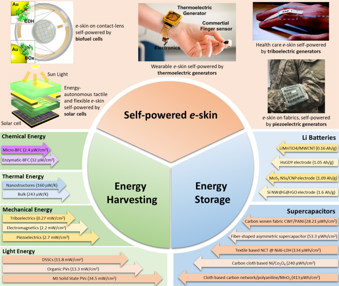
Energy-autonomous electronic skin: potential energy sources. The schematic diagram of self-powered e-skin,
comprising: (i) energy harvesting (light, mechanical, chemical and
thermal energy), (ii) energy storage (batteries and supercapacitors) and
(iii) examples of self-powered e-skin solutions. Energy
harvesting: the illustration compiles the best performance energy
harvesters and their corresponding energy outcome (i.e. power density)
depending on the energy source (light, mechanical, chemical and thermal energy),
highlighting successful devices exhibiting features including
stretchability, lightweight, output powers and wearability. Energy
storage: highlighting various flexible active electrodes that enhance
the performance of LiBs and textile/fibre/cloth-based supercapacitors for wearable systems. Examples of self-powered e-skin
solutions: the illustration shows representative examples of electronic
devices continuously self-powered by various energy sources, including
tactile e-skin for robots self-powered by sunlight.
summarizes the state-of-the art energy harvesting and storage technologies successfully utilized in e-skin-like systems such as graphene-based tactile skin powered by sunlight, a pulse oximeter powered by thermal energy from human body, healthcare e-patch powered by human finger vibrations and multi-sensing e-skin on fabrics powered by human arm actions.The best reported performances (e.g. power density and capacity) . The energy harvesting, and storage solutions on their suitability for a wide range of e-skin applications.
The following section presents the advances in the energy harvesting with particular focus on the solutions relevant to e-skin.
This is followed by a discussion in the section 'Towards continuous
energy supply: technologies for energy storage and wireless charging' on
the energy storage and transmission technologies, including wireless
energy transfer. Few examples of self-powered e-skin systems are presented in the section 'Self-powered e-skin'.
The key challenges and potential solutions, critical design strategies,
and most promising materials for the development of energy-autonomous e-skin have been discussed in the section 'Key challenges and potential solutions for future self-powered e-skin' . With several reviews on e-skin focussing on the sensing and electronics components only,
the most promising energy sources available in the ambient for self-powering of e-skin and other similar technologies presented in the section 'Self-powered e-skin'.
The fundamental mechanism behind each type energy-harvesting method,
their approximate energy budget, i.e. power conversion efficiency (PCE)
and power density (PD), etc. are thoroughly discussed. Since several
applications require e-skin to be flexible or to conform to 3D
surfaces, the discussion here considers the energy-harvesting solutions
with features such as bendability, conformability, wearability,
stretchability, and compatibility to low-temperature fabrication
procedures.
Light energy
Among all, solar energy is one of the most abundant renewable energies available from the environment. The solar energy that is provided to the earth surface during 1 h exceeds by far the energy consumed globally by humans in 1 year. This is the main reason to consider light energy as a potential source for self-powered systems. A solar-powered e-skin integrated on the body of a robot would allow the robot to execute tasks in wide ranging environments, either on the Earth or in space, thanks to the great amount of energy supplied by the sun.Photovoltaic (PV) materials that are typically used to transform sunlight energy into electricity are based on semiconductor solid-state thin films made of crystalline Si (c-Si), amorphous-Si (a-Si), polycrystalline-Si (poly-Si) and monocrystalline Si (mc-Si).Flexible PV cells, which could meet the conformability requirements of e-skin, have also been fabricated successfully using a-Si (PCE ~ 8%), and enormous effort is being put to fabricate the new generation of low-cost PV cells with higher PCE, lightweight, and using print technology. These technologies mainly include dye-sensitized PV cells and the PV cells based on organic materials, quantum dots and perovskites. The lightweight, conformability, compatibility to low-temperature processing and to textile/fabrics like substrates of PV cells, mechanical strength, low-cost fabrication process, and biocompatibility (e.g. for e-skin applications on humans or animals) are also crucial properties for the use of PVs as energy source in portable and wearable self-powered e-skin.61 For the sake of comparison, the PCE (obtained using an A.M. 1.5 solar illumination with 100 mW/cm2 intensity) of various PV technologies
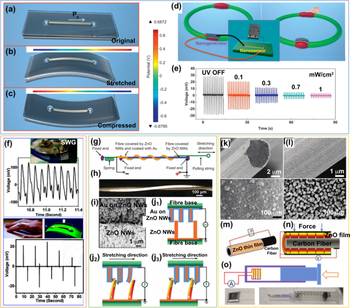
Piezoelectric energy generators. a 3D schema of a single NW-based piezoelectric nanogenerator fabricated on a flexible substrate and subjected to b stretching and c compression conditions. d 3D schema presenting the working principle of a self-powered touch nano-sensors powered by a piezoelectric nanogenerator .
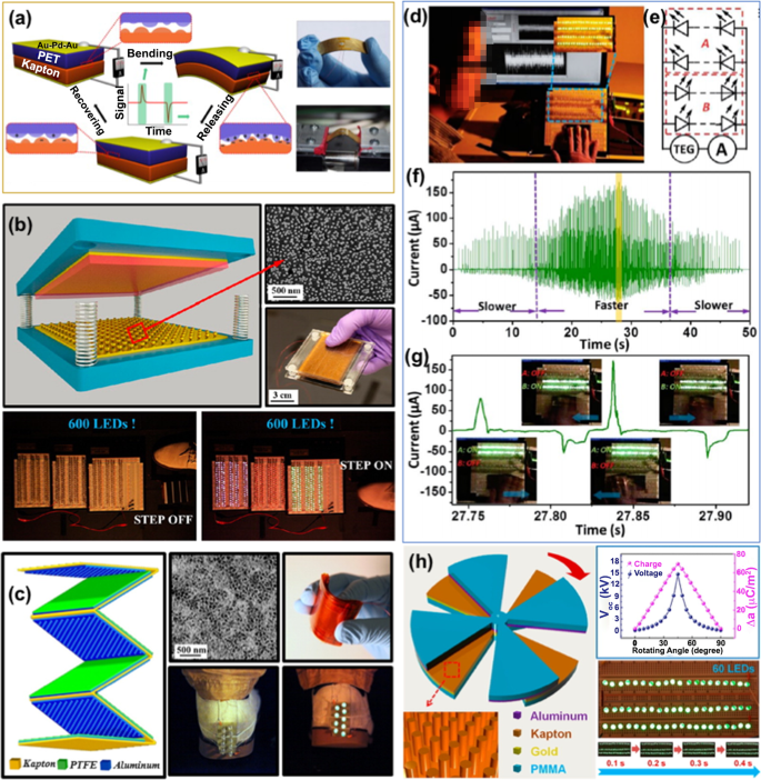
Triboelectric energy generators. a 3D schema (left) and photograph (right) of flexible TEG under bending conditions.
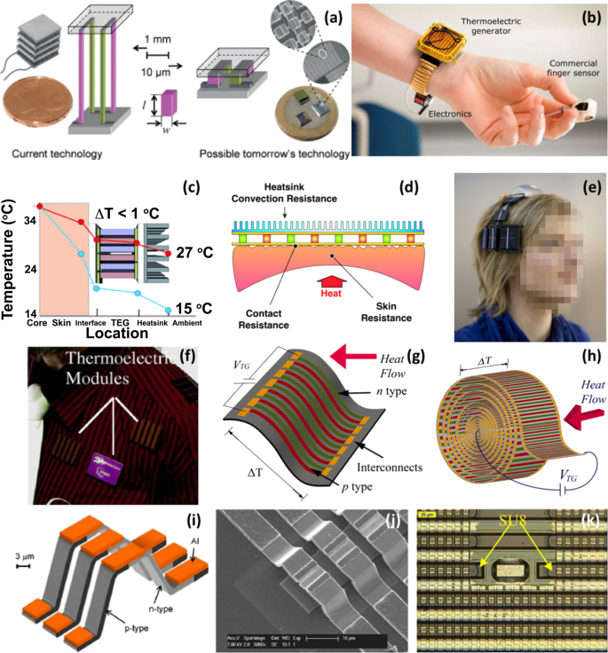
Thermal energy generators. a Current (left) and futuristic (right) view of TE generators. b Body-powered wireless pulse oximeter. c Temperature difference from core body to the ambient air.
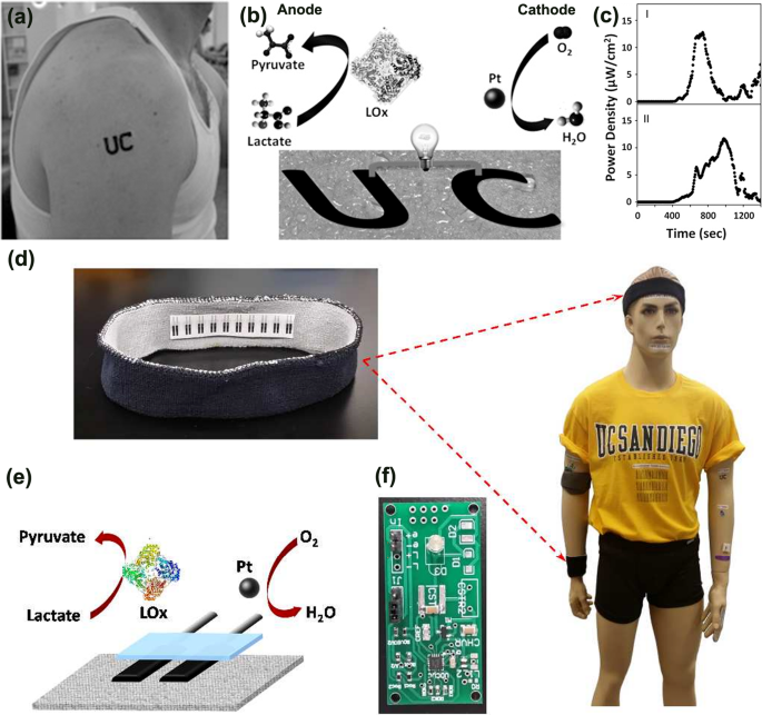
Chemical energy generators. a Photograph of a UC-inspired tBFC integrated on the deltoid of a volunteer.
In e-skin applications, the use of soft and stretchable electronics is common because it improves the conformability. BFCs have also demonstrated great applicability as they meet such requirements due to their biocompatibility, flexibility/stretchability, and scalability towards high-power-density generation, compatibility to soft substrate to minimize the impact on skin irritation and wearers comfort. For such wearable systems, an alternative approach consisting of a layered flexible biofuel based on biobattery with bioanode fabrics for fructose oxidation, hydrogel sheets containing fructose as fuel, and O2-diffusion biocathode fabrics, has also been reported with maximum power of 0.64 mW at 1.21 V. High energy density and stretchability are the key challenges for this type of biofuels. Highly stretchable textile BFCs have been fabricated by screen printing of stretchable inks with CNT and Ag2O/Ag electrodes, exhibiting stable power outputs after 100 cycles of 100% stretching. The fabricated BFCs produces power densities of 160 and 250 mW/cm2 with single-enzyme and membrane-free configurations, respectively, and potential application for self-powered biosensors. In this regard, stretchability feature is currently a matter of intensive investigations in BFCs due to the possibility to complement other technologies such as energy storage devices and sensors currently fabricated on stretchable substrates.
Towards continuous energy supply: technologies for energy storage and wireless charging
While the efficient harvesting and management of renewable energy sources available in the environment (see the section 'Sources of electrical energy'), are key to the development of self-powered systems (see the section 'Self-powered e-skin'), ensuring the continuous supply of energy is also important. To this end, the e-skin should also have suitable scheme for energy storage and among various solutions available today the flexible batteries and supercapacitors are the most promising as summarized . The integration of both energy harvesting and storage technologies forming a self-powered pack (SPP), is currently an intensive subject of investigation due to its tremendous potential for wearable systems.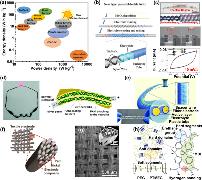
Energy storage devices. a Comparison between batteries and SC technologies performance. b 3D schema of wire-shaped SCs. c Flexible wire-shaped SC characterized under different bending conditions.
One of the main drawbacks of the current portable energy storage technology for e-skin
and wearable systems is the high dependence on bulky wires for energy
transfer, which hinders the portability and autonomy. The wearable
systems including sensors for health monitoring electronic patches, and e-skin
for robots and artificial limbs, require a drastic reduction of wires
density (and size), or even the development of a wireless energy
transfer technology. Electric vehicles, robots, or artificial limbs are
good examples of applications that would strongly benefit by flexible
and low-weight energy storage and wireless energy transfer technologies.
Supercapacitors
Supercapacitors (SCs) have emerged as a promising energy storage alternative to the conventional Li-batteries (LiB), mainly due to properties such as high energy density (17.6 Wh/kg), power density (98 kW/kg), specific capacitance (790 F/g), volumetric capacitance (205.4 F/cm3), lightweight (10 mg), flexibility (capacitance change <1% under bending angles of 180°) , cyclic stability (98.3% capacitance retention after 5000 charge/discharge cycles) and stretchability (~30%) , State-of-art SCs are generally made of conductive polymers , metal oxides nanostructures, carbon-based materials (carbon nanotubes (CNTs) and graphene), or hybrid combination of these materials . In addition to their excellent energy storage capacity, the SCs are also exceptional because of their quick energy delivery (charging/discharging rates ~50 V/s).This is an attractive feature as in addition to enabling continuous operation of e-skin, the SCs could also allow provide energy to operate actuators in artificial limbs in prosthesis and robotics. Further, the fabrication of SCs on non-conventional substrates such as clothes, glove, woven and fabric materials, make them a promising candidate for application such as wearable systems or e-skin for fashion industry. In this regard, the fabrication of flexible SCs has been demonstrated by integrating electrochemically active materials such as metal oxides and conducting polymers with flexible fibres made of graphene, carbon, metal and plastic.Wearable batteries
Conventional batteries present drawbacks such as lack of flexibility/stretchability, bulkiness, heavy weight and generation of heat, which have encouraged researchers to investigate alternative energy storage devices such SCs described in previous section. However, due to significantly higher energy density than the state-of-art SCs (e.g. LiCoO2 // Graphite: 387 Wh/kg, R-Na2Fe2(CN) // Cu: 336 Wh/kg, LiMn2O4 // Graphite: 300 Wh/kg), there is still a strong belief that next generation of batteries with flexible and stretchable form factors is possible. Accordingly, the strategies that are being followed today include using new materials and configurations of the battery components, i.e. current collector, binder and separator, and their role into the mechanical endurance of the battery electrodes, to preserve or enhance the resulting energy storage capacity. For example, a battery consisting of a current collector made of Ni-coated polyester yarn, and binder and separator made of polyurethane (PU) has shown a great enhancement of the electrode mechanical strength, also exhibiting good flexibility . The PU separator consists of hard and soft domains that prove mechanical strength and flexibility, respectively, to the overall structure of the battery, which are desirable features for its use in the wearable systems. In addition, the PU separators have also demonstrated a significant enhancement of the ionic exchange for the electronic reaction, benefiting the energy storage mechanism. PU also exhibits a superior resistance against thermal shrinkage at high temperatures, which expands further the thermal breakage window of the battery.The use of CNTs has also been probed for flexible batteries. For example, CNTs-based thin films have been utilized either as current collector with plain paper as a separator (108 mAh/g), or in hybrid electrodes consisting of ultra-long CNTs and V2O5 NWs (169 mAh/g), or in LiMnTiO4/MWCNT-based electrodes (161 mAh/g), and in sodium 1,4-dioxonaphthalene-2-sulfonate and MWNTs electrodes (155 mAh/g).
The conventional LiBs do not offer good alternative to above solutions for continuous powering of e-skin as, in addition to the mechanical rigidity, they use toxic and/or environment unfriendly electrolytes, which drastically hinder their practical applicability in wearable systems. A common issue observed in LiBs is related to the uncontrolled growth of dendritic Li on the anode surface during the over-charge process, causing the undesired both the short-circuiting of battery electrodes, and the generation of heat. To overcome these drawbacks, more stable materials such as Li4Ti5O12 (LTO) and LiMn2O4 (LMO), have been investigated as they exhibit minor volume changes under several charging/discharging cycles. LiBs have also been made from LTO and LMO nanoparticles integrated into two aligned MWCNT yarns, which act as anode and cathode. The fabricated wire-shaped LiBs exhibit energy densities of 27 Wh/kg (17.7 mWh/cm3), power densities of 880 W/kg (0.56 W/cm3), and 97% of capacity retention after 1000 bending cycles.
Recently, Zn–air batteries (ZAB) have emerged as a potential environmental friendly alternative of LiBs, mainly due to their high theoretical energy densities (1084 Wh/kg) which are about an order of magnitude higher than LiBs. Flexible fibre-shaped ZAB knitted into clothes and textiles have been successfully reported to exhibit energy densities of around 649 mWh/g. The connection of three fibre-shaped ZABs knitted in series holds a potential of 3.59 V which is sufficient for powering micro- and nano-devices.
Future advances in the e-skin will focus on the complex integration of active/passive components such as sensors, actuators, diodes, transistors, integrated circuits on stretchable substrates. In this scenario, the conformability of the e-skin constituents will be crucial for their applicability as artificial skin in a wide range of applications. In spite of the extensive efforts to advance stretchable electronics, there is still no great solutions for integrating durable/stable energy storage devices on stretchable substrates. In this regard, the works on dry gel cells based on arrays of batteries embedded in a single elastomer matrix could be interesting direction. These batteries have been demonstrated to withstand stretch ratio up to 100% before failure, delivering open-circuit voltage close to 1.5 V and short-circuit currents up to 30 mA. In addition, these dry gel cells have shown lifetimes above 1000 h and high capacities of 3.5 mAh/cm2. The experimental process employed to fabricate these cells are compatible with roll-to-roll techniques, which makes this technology promising for the low-cost production of self-powered stretchable systems.
Wireless energy transfer
For future advances in the field of self-powered systems, there is a growing interest on wireless power transfer (WPT) technologies, to allow the wireless charging of energy storage devices and also the wireless use of the stored energy by wearable electronics such as multi-sensing devices in e-skin. The magnetic resonate coupling and near-field inductive technologies, also known as near-field communication (NFC), are the two key approaches for WPT. The excellent progress achieved in the field is evident from the WPT-based low-cost and portable modules already available in the market and the growing number of intellectual properties. However, much progress is required, especially to design high energy density devices for implantable applications and for high transfer efficiency. The possibility of charging batteries or SCs through WPT technologies will have tremendous advantage for portable and autonomous systems in a broad number of applications and high commerciality in the market of near-future wearable systems.Recently, some works have been reported in the area of wireless energy transfer, including SCs directly charged through WPT technologies. For example, nerve simulator applications consisting of a SC with an energy of 860 mJ and a maximum capacitance of 0.2 F, which can be quickly (<2 min) and fully charged through a WPT, and then continuously utilized for 33 h (when connecting micro- and nano-devices loads). Furthermore, a wearable textile antenna has exhibited reasonable good performance in WPT through magnetic resonance mechanism. With four planar spiral coils embroidered with conductive threads, this WPT system could transfer a total power of 12.75 mW with an amplitude of 5.51 dB along a large distance of 15 cm. Nowadays, WPT technology is moving towards the development of high-performance systems with great transfer efficiency and along longer energy transfer distances. In this scenario, much progress will be required in WPT research area, especially in designing architectures (e.g. discovering new materials), high energy density energy storage devices for implantable applications.
Great efforts have been dedicated on the optimization of WPT. Accordingly, NFC technologies has emerged as a promising alternative to achieve the effective transfer of power, e.g. between the energy harvester and energy storage device (charging) or between the energy storage device and the e-skin active and passive elements (powering). Both impedance and resonant frequency characteristic of NFC power transfer systems have been investigated to improve the coupling distance resulting in the minor loss of power. As examples of achievements in the field, WPT based on NFC have been successfully utilized in both bio-implantable chips and electric vehicles. These achievements are promising for the self-powered e-skin applications covered in this work, where distance between different elements distributed/stacked along the structure of the e-skin (sensors, harvesters, storage devices, etc.) are in the typical range of NFC technology.
Wireless powering of sensors is currently an intensive matter of investigation. The current advances related to the design and development of sensors on non-conventional flexible/stretchable substrates, have opened promising alternatives to distribute more number of thin, soft and skin-like sensors along human or robotic body. The distribution of these sensors along either robotic or human bodies would a continuous measurement of interactions of robot with the environment (touch sensors, proximity sensors, etc.) or spatiotemporal mapping of physiological health of humans—the latter being relevant for healthcare (electrochemical sensors, temperature sensors, etc.). However, the greater number of skin-like sensors distributed along the body, the more challenging it becomes to deliver the required power. In order to overcome this challenge, new materials and designs are being studied theoretically and experimentally to reduce the total power consumption of sensors and to allow the wireless delivery of power to acquire sensors data. These investigations have focused on the development of free-battery autonomous multi-sensing e-skin (i.e. network of electronic devices sensitive to different stimulus in the environment) covering a human body with low-power pressure and temperature sensors (total of 65 sensors distributed along the subject body). The skin is capable of monitoring wirelessly the local pressure and temperature of human subjects sleeping in a hospital bed. Multiple large-scale loop antennas interfaced to radio-frequency (RF) power delivery and data acquisition electronics allow multiplexed operation with a range of tens of centimetres. Output of these sensors were compared with computational modelling, offering a spatiotemporal mapping of physiological processes. Such energy-autonomous sensing e-skin could reduce the nursing labour required in a hospital and allow monitoring of multiple patients without the need of expensive beds or complex instrumentation.
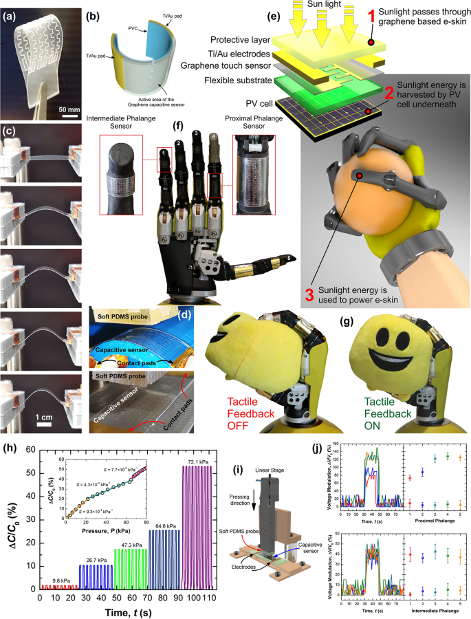
Touch sensitive e-skin powered by light energy
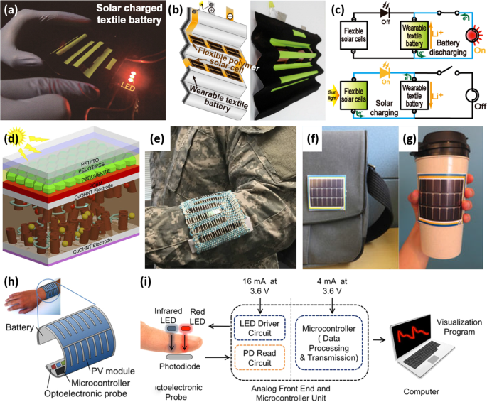
Self-powered packs (SPP).
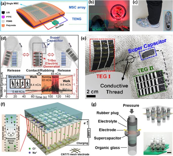
Self-powered wearable e-skin: self-charging devices
This
review analyses the most promising energy harvesting and storage
technologies to highlight the development of a compact energy system for
energy-autonomous e-skin. The in-depth discussion on various
energy sources (e.g. sunlight, mechanical, thermal, and chemical) and
storage methods (batteries, supercapacitors, etc.), as well as, energy
transfer through wireless technologies, highlights suitable options for
continuous operation of multiple electronic devices and sensors
distributed along the e-skin. As explained in this review, the
use of hybrid energy systems made from the combination of two or more
energy-harvesting mechanisms, will result in a new advanced technology
capable to work continuously with stability, even during the short
absence of some of energy sources.
Advanced new materials and structures leading to higher power conversion efficiencies from light, mechanical, thermal, and chemical energy sources to electricity, are likely to appear next, which will allow reduction of cost, size and weight of next generation of energy harvesters. In this scenario, both organic and inorganic materials with the shape of nanostructures are promising candidates for the development of near-future PVs, piezoelectronics, triboelectronics, thermoelectric generators, etc. Some of the above energy-harvesting technologies, which were covered in this review, have already reached the market, and have been successfully developed on flexible/stretchable and light-weight substrates. This new technology will offer an excellent opportunity for the development of self-powered systems, e.g. for e-skin, wearable patches, smart-devices, etc. for different applications (robotics, human health monitoring, environmental monitoring, etc.). Apart from above energy sources, tremendous potential lies in the field of biofuels to power e-skin used for human health monitoring.
These new technologies combined with a rapid development in the field of energy storage devices such as supercapacitors or ultracapacitors combined with progresses in the field of wireless energy transmission, will produce a significant growth in the field of self-powered systems. Especially for e-skin applications, where the energy requirements of distributed sensing/electronic components are in the range of hundreds of nanowatts. Finally, the integration of energy systems (i.e. harvester, storage, and transmitter) with e-skin will allow continuous powering of various components, thus improving the user acceptability of this interesting technology.
__________________________________________________________________________________
Artificial intelligence and the future of work

Automation, artificial intelligence, and the essential role of humans
that artificial
intelligence threatens to automate away all the work that people do. But
what if there's a way to rethink the concept of "work" that not only
makes humans essential, but allows them to take fuller advantage of
their uniquely human abilities?
Will
pessimistic predictions of the rise of the robots come true? Will
humans be made redundant by artificial intelligence (AI) and robots,
unable to find work and left to face a future defined by an absence of
jobs? Or will the optimists be right? Will historical norms reassert
themselves and technology create more jobs than it destroys, resulting
in new occupations that require new skills and knowledge and new ways of
working?
It is possible that the most effective use of AI is not simply as a means to automate more tasks, but as an enabler to achieve higher-level goals, to create more value. The advent of AI makes it possible—indeed, desirable—to reconceptualize work, not as a set of discrete tasks laid end to end in a predefined process, but as a collaborative problem-solving effort where humans define the problems, machines help find the solutions, and humans verify the acceptability of those solutions.
Constructing work
Pre-industrial work was constructed around the product, with skilled artisans taking responsibility for each aspect of its creation. Early factories (commonly called manufactories at the time) were essentially collections of artisans, all making the same product to realize sourcing and distribution benefits. In contrast, our current approach to work is based on Adam Smith’s division of labor,1 in the form of the task. Indeed, if we were to pick one idea as the foundation of the Industrial Revolution it would be this division of labor: Make the coil spring rather than the entire watch.Specialization in a particular task made it worthwhile for workers to develop superior skills and techniques to improve their productivity. It also provided the environment for the task to be mechanized, capturing the worker’s physical actions in a machine to improve precision and reduce costs. Mechanization then begat automation when we replaced human power with water, then steam, and finally electric power, all of which increased capacity. Handlooms were replaced with power looms, and the artisanal occupation shifted from weaving to managing a collection of machines. Human computers responsible for calculating gunnery and astronomical tables were similarly replaced with analog and then digital computers and the teams of engineers required to develop the computer’s hardware and software. Word processors shifted responsibility for document production from the typing pool to the author, resulting in the growth of departmental IT. More recently, doctors responsible for interpreting medical images are being replaced by AI and its attendant team of technical specialists.
This impressive history of industrial automation has resulted not only from the march of technology, but from the conception of work as a set of specialized tasks. Without specialization, problems wouldn’t have been formalized as processes, processes wouldn’t have been broken into well-defined tasks, and tasks wouldn’t have been mechanized and then automated. Because of this atomization of work into tasks (conceptually and culturally), jobs have come to be viewed largely as compartmentalized collections of tasks. (Typical corporate job descriptions and skills matrices take the form of lists of tasks.) Job candidates are selected based on their knowledge and skills, their ability to prosecute the tasks in the job description. A contemporary manifestation of this is the rise of task-based crowdsourcing sites—such as TaskRabbit3 and Kaggle,4 to name only two—that enable tasks to be commoditized and treated as piecework.
Does automation destroy or create jobs?
AI demonstrates the potential to replicate even highly complex, specialized tasks that only humans were once thought able to perform (while finding seemingly easy but more general tasks, such as walking or common sense reasoning, incredibly challenging). Unsurprisingly, some pundits worry that the age of automation is approaching its logical conclusion, with virtually all work residing in the ever-expanding domain of machines. These pessimists think that robotic process automation (RPA) and such AI solutions as autonomous vehicles will destroy jobs, relegating people to filling the few gaps left in the economy that AI cannot occupy. There may well be more jobs created in the short term to build, maintain, and enhance the technology, but not everyone will be able to gain the necessary knowledge, skills, and experience.For example, it seems unlikely that the majority of truck, bus, or taxi drivers supplanted by robots will be able to learn the software development skills required to build or maintain the algorithms replacing them.Further, these pessimists continue, we must consider a near future where many (if not all) low-level jobs, such as the administrative and process-oriented tasks that graduates typically perform as the first step in their career, are automated. If the lower levels of the career ladder are removed, they will likely struggle to enter professions, leaving a diminishing pool of human workers to compete for a growing number of jobs. Recent advances in AI prompt many to wonder just how long it will be before AI catches up with the majority of us. How far are we from a future where the only humans involved with a firm are its owners?
Of course, there is an alternative view. History teaches that automation, far from destroying jobs, can and usually does create net new jobs, and not just those for building the technology or training others in its use. This is because increased productivity and efficiency, and the consequent lowering of prices, has historically led to greater demand for goods and services. For example, as the 19th century unfolded, new technology (such as power looms) enabled more goods (cloth, for instance) to be produced with less effort; as a consequence, prices dropped considerably, thus increasing demand from consumers. Rising consumer demand not only drove further productivity improvements through progressive technological refinements, but also significantly increased demand for workers with the right skills.8 The optimistic view holds that AI, like other automation technologies before it, will operate in much the same way. By automating more and more complex tasks, AI could potentially reduce costs, lower prices, and generate more demand—and, in doing so, create more jobs.
The productivity problem and the end of a paradigm
Often overlooked in this debate is the assumption made by both camps that automation is about using machines to perform tasks traditionally performed by humans. And indeed, the technologies introduced during the Industrial Revolution progressively (though not entirely) did displace human workers from particular tasks.9 Measured in productivity terms, by the end of the Industrial Revolution, technology had enabled a weaver to increase by a factor of 50 the amount of cloth produced per day;10 yet a modern power loom, however more efficient, executes the work in essentially the same way a human weaver does. This is a pattern that continues today: For example, we have continually introduced more sophisticated technology into the finance function (spreadsheets, word processing, and business intelligence tools are some common examples), but even the bots of modern-day robotic process automation complete tasks in the conventional way, filling in forms and sending emails as if a person were at the keyboard, while “exceptions” are still handled by human workers.We are so used to viewing work as a series of tasks, automation as the progressive mechanization of those tasks, and jobs as collections of tasks requiring corresponding skills, that it is difficult to conceive of them otherwise. But there are signs that this conceptualization of work may be nearing the end of its useful life. One such major indication is the documented fact that technology, despite continuing advances, no longer seems to be achieving the productivity gains that characterized the years after the Industrial Revolution. Short-run productivity growth, in fact, has dropped from 2.82 (1920–1970) to 1.62 percent (1970–2014). Many explanations for this have been proposed, including measurement problems, our inability to keep up with the rapid pace of technological change, and the idea that the tasks being automated today are inherently “low productivity.”12 In The Rise and Fall of American Growth, Robert Gordon argues that today’s low-productivity growth environment is due to a material difference in the technologies invented between 1850 and 1980 and those invented more recently. Gordon notes that prior to the Industrial Revolution mean growth was 1.79 percent (1870–1920), and proposes that what we’re seeing today is a reversion to this mean.
None of these explanations is entirely satisfying. Measurement questions have been debated to little avail. And there is little evidence that technology is developing more rapidly today than in the past.15 Nor is there a clear reason for why, say, a finance professional managing a team of bots should not realize a similar productivity boost as a weaver managing a collection of power looms. Even Robert Gordon’s idea of one-time technologies, while attractive, must be taken with a grain of salt: It is always risky to underestimate human ingenuity.
One explanation that hasn’t been considered, however, is that the industrial paradigm itself—where jobs are constructed from well-defined tasks—has simply run its course. We forget that jobs are a social construct, and our view of what a job is, is the result of a dialogue between capital and labor early in the Industrial Revolution. But what if we’re heading toward a future where work is different, rather than an evolution of what we have today?
Suitable for neither human nor machine
Constructing work around a predefined set of tasks suits neither human nor machine. On one hand, we have workers complaining of monotonous work,16 unreasonable schedules, and unstable jobs.17 Cost pressure and a belief that humans are simply one way to prosecute a task leads many firms to slice the salami ever more finely, turning to contingent labor and using smaller (and therefore more flexible) units of time to schedule their staff. The reaction to this has been a growing desire to recut jobs and make them more human, designing new jobs that make the most of our human advantages (and thereby make us humans more productive). On the other hand, we have automation being deployed in a manner similar to human labor, which may also not be optimal.The conundrum of low productivity growth might well be due to both under-utilized staff and under-utilized technology. Treating humans as task-performers, and a cost to be minimized, might be conventional wisdom, but Zeynep Ton found (and documented in her book The Good Jobs Strategy) that a number of firms across a range of industries—including well-known organizations such as Southwest Airlines, Toyota, Zappos, Wegmans, Costco, QuikTrip, and Trader Joe’s—were all able to realize above-average service, profit, and growth by crafting jobs that made the most of their employees’ inherent nature to be social animals and creative problem-solvers.18 Similarly, our inability to realize the potential of many AI technologies might not be due to the limitations of the technologies themselves, but, instead, our insistence on treating them as independent mechanized task performers. To be sure, AI can be used to automate tasks. But its full potential may lie in putting it to a more substantial use.
There are historical examples of new technologies being used in a suboptimal fashion for years, sometimes decades, before their more effective use was realized.19 For example, using electricity in place of steam in the factory initially resulted only in a cleaner and quieter work environment. It drove a productivity increase only 30 years later, when engineers realized that electrical power was easier to distribute (via wires) than mechanical power (via shafts, belts, and pulleys). The single, centralized engine (and mechanical power distribution), which was a legacy of the steam age, was swapped for small engines directly attached to each machine (and electrical power distribution). This enabled the shop floor to be optimized for workflow rather than power distribution, delivering a sudden productivity boost.
A new line between human and machine
The question then arises: If AI’s full potential doesn’t lie in automating tasks designed for humans, what is its most appropriate use? Here, our best guidance comes from evidence that suggests human and machine intelligence are best viewed as complements rather than substitutes20—and that humans and AI, working together, can achieve better outcomes than either alone.21 The classic example is freestyle chess. When IBM’s Deep Blue defeated chess grandmaster Garry Kasparov in 1997, it was declared to be “the brain’s last stand.” Eight years later, it became clear that the story is considerably more interesting than “machine vanquishes man.” A competition called “freestyle chess” was held, allowing any combination of human and computer chess players to compete. The competition resulted in an upset victory that Kasparov later reflected upon:
The surprise came at the conclusion of the
event. The winner was revealed to be not a grandmaster with a
state-of-the-art PC but a pair of amateur American chess players using
three computers at the same time. Their skill at manipulating and
“coaching” their computers to look very deeply into positions
effectively counteracted the superior chess understanding of their
grandmaster opponents and the greater computational power of other
participants. Weak human + machine + better process was superior to a
strong computer alone and, more remarkably, superior to a strong human +
machine + inferior process… Human strategic guidance combined with the
tactical acuity of a computer was overwhelming.
The lesson here is that human and machine intelligence are different
in complementary, rather than conflicting, ways. While they might solve
the same problems, they approach these problems from different
directions. Machines find highly complex tasks easy, but stumble over
seemingly simple tasks that any human can do. While the two might use
the same knowledge, how they use it is different. To realize the most
from pairing human and machine, we need to focus on how the two
interact, rather than on their individual capabilities.Tasks versus knowledge
Rather than focusing on the task, should we conceptualize work to focus on the knowledge, the raw material common to human and machine? To answer this question, we must first recognize that knowledge is predominantly a social construct, one that is treated in different ways by humans and machines.Consider the group of things labeled “kitten.” Both human and robot learn to recognize “kitten” the same way: by considering a labeled set of exemplars (images). However, although kittens are clearly things in the world, the concept of “kitten”—the knowledge, the identification of the category, its boundaries, and label—is the result of a dialogue within a community .
Much of what we consider to be common sense is defined socially. Polite behavior, for example, is simply common convention among one’s culture, and different people and cultures can have quite different views on what is correct behavior (and what is inexcusable). How we segment customers; the metric system along with other standards and measures; how we decompose problems into business processes and the tasks they contain; measure business performance; define the rules of the road and drive cars; regulation and legislation in general; and the cliché of Eskimos having dozens, if not hundreds, of words for snow, all exemplify knowledge that is socially constructed. Even walking—and the act of making a robot walk—is a social construct, as it was the community that identified “walking” as a phenomenon and gave it a name, ultimately motivating engineers to create a walking robot, and it’s something we and robots learn by observation and encouragement. There are many possible ways of representing the world and dividing up reality, to understand the nature and relation of things, and to interact with the world around us, and the representation we use is simply the one that we agreed on. Choosing one word or meaning above the others has as much to do with societal convention as ontological necessity.
Socially constructed knowledge can be described as encultured knowledge, as it is our culture that determines what is (and what isn’t) a kitten, just as it is culture that determines what is and isn’t a good job. (We might even say that knowledge is created between people, rather than within them.) Encultured knowledge extends all the way up to formal logic, math, and hard science. Identifying and defining a phenomenon for investigation is thus a social process, something researchers must do before practical work can begin. Similarly, the rules, structures, and norms that are used in math and logic are conventions that have been agreed upon over time. A fish is a fish insofar as we all call it a fish. Our concept of “fish” was developed in dialogue within the community. Consequently, our concept of fish drifts over time: In the past “fish” included squid (and some other, but not all, cephalopods), but not in current usage. The concepts that we use to think, theorize, decide, and command are defined socially, by our community, by the group, and evolve with the group.
Knowledge and understanding
How is this discussion of knowledge related to AI? Consider again the challenge of recognizing images containing kittens. Before either human or machine can recognize kittens, we need to agree on what a “kitten” is. Only then can we collect the set of labeled images required for learning.The distinction between human and machine intelligence, then, is that the human community is constantly constructing new knowledge (labeled exemplars in the case of kittens) and tearing down the old, as part of an ongoing dialogue within the community. When a new phenomenon is identified that breaks the mold, new features and relationships are isolated and discussed, old ones reviewed, concepts shuffled, unlearning happens, and our knowledge evolves. The European discovery of the platypus in 1798 is a case in point. When Captain John Hunter sent a platypus pelt to Great Britain, many scientists’ initial hunch was that it was a hoax. One pundit even proposed that it might have been a novelty created by an Asian taxidermist (and invested time in trying to find the stitches). The European community didn’t know how to describe or classify the new thing. A discussion ensued, new evidence was sought, and features identified, with the community eventually deciding that the platypus wasn’t a fake, and our understanding of animal classification evolved in response.
Humans experience the world in all its gloriously messy and poorly defined nature, where concepts are ill-defined and evolving and relationships fluid. Humans are quite capable of operating in this confusing and noisy world; of reading between the lines; tapping into weak signals; observing the unusual and unnamed; and using their curiosity, understanding, and intuition to balance conflicting priorities and determine what someone actually meant or what is the most important thing to do. Indeed, as Zeynep Ton documented in The Good Jobs Strategy, empowering employees to use their judgment, to draw on their own experience and observations, to look outside the box, and to consider the context of the problem they are trying to understand (and solve), as well as the formal metrics, policies, and rules of the firm, enabled them to make wiser decisions and consequentially deliver higher performance. Unfortunately, AI doesn’t factor in the unstated implications and repercussions, the context and nuance, of a decision or action in the way humans do.
It is this ability to refer to the context around an idea or problem—to craft more appropriate solutions, or to discover new knowledge to create (and learn)—that is uniquely human. Technology cannot operate in such an environment: It needs its terms specified and objectives clearly articulated, a well-defined and fully contextualized environment within which it can reliably operate. The problem must be identified and formalized, the inputs and outputs articulated, before technology can be leveraged. Before an AI can recognize kittens, for instance, we must define what a kitten is (by exemplar or via a formal description) and find a way to represent potential kittens that the AI can work with. Similarly, the recent boom in autonomous vehicles is due more to the development of improved sensors and hyper-accurate maps, which provide the AI with the dials and knobs it needs to operate, than the development of vastly superior algorithms.
It is through the social process of knowledge construction that we work together to identify a problem, define its boundaries and dependences, and discover and eliminate the unknowns until we reach the point where a problem has been defined sufficiently for knowledge and skills to be brought to bear.
A bridge between human and machine
Consider the question of what a “happy retirement” is: We all want one, but we typically can’t articulate what it is. It’s a vague and subjective concept with a circular definition: A happy retirement is one in which you’re happy. Before we can use an AI-powered robo-advisor to create our investment portfolio, we need to take our concept of a “happy retirement” through grounding the concept (“what will actually make me happy, as opposed to what I think will make me happy”), establishing reasonable expectations (“what can I expect to fund”), to attitudes and behaviors (“how much can I change my habits, how and where I spend my money, to free up cash to invest”), before we reach the quantifiable data against which a robo-advisor can operate (investment goals, income streams, and appetite for risk). Above quantifiable investment goals and income streams is the social world, where we need to work with other people to discover what our happy retirement might be, to define the problem and create the knowledge. Below is where automation—with its greater precision and capacity for consuming data—can craft our ultimate investment strategy. Ideally there is interaction between the two layers—as with freestyle chess—with automation enabling the humans to play what-if games and explore how the solution space changes depending on how they shape the problem definition.
Reconstructing work
The foundation of work in the pre-industrial, craft era was the product. In the industrial era it is the task, specialized knowledge, and skills required to execute a step in a production process. Logically, the foundation of post-industrial work will be the problem—the goal to be achieved —one step up from the solution provided by a process.If we’re to organize work around problems and successfully integrate humans and AI into the same organization, then it is management of the problem definition—rather than the task as part of a process to deliver a solution—that becomes our main concern. Humans take responsibility for shaping the problem—the data to consider, what good looks like, the choices to act—which they do in collaboration with those around them and their skill in doing this will determine how much additional value the solution creates. Automation (including AI) will support the humans by augmenting them with a set of digital behaviors (where a behavior is the way in which one acts in response to a particular situation or stimulus) that replicate specific human behaviors, but with the ability to leverage more data and provide more precise answers while not falling prey to the various cognitive biases to which we humans are prone. Finally, humans will evaluate the appropriateness and completeness of the solution provided and will act accordingly.
Indeed, if automation in the industrial era was the replication of tasks previously isolated and defined for humans, then in the post-industrial era, automation might be the replication of isolated and well-defined behaviors that were previously unique to humans.
Integrating humans and AI
Consider the challenge of eldercare. A recent initiative in the United Kingdom is attempting to break down the silos in which specialized health care professionals currently work. Each week, the specialists involved with a single patient—health care assistant, physiotherapist, occupational therapist, and so on—gather to discuss the patient. Each specialist brings his or her own point of view and domain knowledge to the table, but as a group they can build a more comprehensive picture of how best to help the patient by integrating observations from their various specialties as well as discussing more tacit observations that they might have made when interacting with the patient. By moving the focus from the tasks to be performed to the problem to be defined―how to improve the patient’s quality of life―the first phase of the project saw significant improvements in patient outcomes over the first nine months.Integrating AI (and other digital) tools into this environment to augment the humans might benefit the patient even more by providing better and more timely decisions and avoiding cognitive biases, resulting in an even higher quality of care. To do this, we could create a common digital workspace where the team can capture its discussions; a whiteboard (or blackboard) provides a suitable metaphor, as it’s easy to picture the team standing in front of the board discussing the patient while using the board to capture important points or share images, charts, and other data. A collection of AI (and non-AI) digital behaviors would also be integrated directly into this environment. While the human team stands in front of the whiteboard, the digital behaviors stand behind it, listening to the team’s discussion and watching as notes and data are captured, and reacting appropriately, or even responding to direct requests.
Data from tests and medical monitors could be fed directly to the board, with predictive behaviors keeping a watchful eye on data streams to determine if something unfortunate is about to happen (similar to how electrical failures can be predicted by looking for characteristic fluctuations in power consumption, or how AI can be used to provide early warning of struggling students by observing patterns in communication, attendance, and assignment submission), flagging possible problems to enable the team to step in before an event and prevent it, rather than after. A speech-to-text behavior creates a transcription of the ensuing discussion so that what was discussed is easily searchable and referenceable. A medical image—an MRI perhaps—is ordered to explore a potential problem further, with the resulting image delivered directly to the board, where it is picked up by a cancer-detection behavior to highlight possible problems for the team’s specialist to review. With a diagnosis in hand, the team works with a genetic drug-compatibility behavior to find the best possible response for this patient and a drug-conflict behavior that studies the patient’s history, prescriptions, and the suggested interventions to determine how they will fit in the current care regime, and explore the effectiveness of different possible treatment strategies. Once a treatment strategy has been agreed on, a planning behavior converts the strategy into a detailed plan—taking into account the urgency, sequencing, and preferred providers for each intervention—listing the interventions to take place and when and where each should take place, along with the data to be collected, updating the plan should circumstances change, such as a medical imaging resource becoming available early due to a cancellation.
Ideally, we want to populate this problem-solving environment with a comprehensive collection of behaviors. These behaviors might be predictive, flagging possible events before they happen. They might enable humans to explore the problem space, as the chess computer is used in freestyle chess, or the drug-compatibility and drug-conflict AIs in the example above. They might be analytical, helping us avoid our cognitive biases. They might be used to solve the problem, such as when the AI planning engine takes the requirements from the treatment strategy and the availability constraints from the resources the strategy requires, and creates a detailed plan for execution. Or they might be a combination of all of these. These behaviors could also include non-AI technologies, such as calculators, enterprise applications such as customer relationship management (CRM) (to determine insurance options for the patient), or even physical automations and non-technological solutions such as checklists.
Uniquely human
It’s important to note that scenarios similar to the eldercare example just mentioned exist across a wide range of both blue- and white-collar jobs. The Toyota Production System is a particularly good blue-collar example, where work on the production line is oriented around the problem of improving the process used to manufacture cars, rather than the tasks required to assemble a car.One might assume that the creation of knowledge is the responsibility of academy-anointed experts. In practice, as Toyota found, it is the people at the coalface, finding and chipping away at problems, who create the bulk of new knowledge. It is our inquisitive nature that leads us to try and explain the world around us, creating new knowledge and improving the world in the process. Selling investment products, as we’ve discussed, can be reframed to focus on determining what a happy retirement might look like for this particular client, and guiding the client to his or her goal. Electric power distribution might be better thought of as the challenge of improving a household’s ability to manage its power consumption. The general shift from buying products to consuming services provides a wealth of similar opportunities to help individuals improve how they consume these services, be they anything from toilet paper subscriptions through cars and eldercare (or other medical and health services) to jet engines, while internally these same firms will have teams focused on improving how these services are created.
Advances (and productivity improvements) are typically made by skilled and curious practitioners solving problems, whether it was weavers in a mill finding and sharing a faster (but more complex) method of joining a broken thread in a power loom or diagnosticians in the clinic noticing that white patches sometimes appear on the skin when melanomas regress spontaneously. The chain of discovery starts at the coalface with our human ability to notice the unusual or problematic—to swim through the stream of the unknowns and of fuzzy concepts that cannot be fully articulated. This is where we collaborate to make sense of the world and create knowledge, whether it be the intimate knowledge of what a happy retirement means for an individual, or grander concepts that help shape the world around us. It is this ability to collectively make sense of the world that makes us uniquely human and separates us from the robots—and it cuts across all levels of society.
If we persist in considering a job to be little more than a collection of related tasks, where value is determined by the knowledge and skill required to prosecute them, then we should expect that automation will eventually consume all available work, as we must assume that any well-defined task, no matter how complex, will be eventually automated. This comes at a high cost, as while machines can learn, they don’t in themselves, create new knowledge. An AI tool might discover patterns in data, but it is the humans who noticed that the data set was interesting and then inferred meaning into the patterns discovered by the machine. As we relegate more and more tasks to machines, we are also eroding the connection between the problems to be discovered and the humans who can find and define them. Our machines might be able to learn, getting better at doing what they do, but they won’t be able to reconceive what ought to be done, and think outside their algorithmic box.
Conclusion
At the beginning , we asked if the pessimists or optimists would be right. Will the future of work be defined by a lack of suitable jobs for much of the population? Or will historical norms reassert themselves, with automation creating more work than it destroys? Both of these options are quite possible since, as we often forget, work is a social construct, and it is up to us to decide how it should be constructed.There is a third option, though: one where we move from building jobs around processes and tasks, a solution that is optimal for neither human nor machine, to building jobs around problems. The difficulty is in defining production as a problem to be solved, rather than a process to be streamlined. To do this, we must first establish the context for the problem (or contexts, should we decompose a large production into a set of smaller interrelated problems). Within each context, we need to identify what is known and what is unknown and needs to be discovered. Only then can we determine for each problem whether human or machine, or human and machine, is best placed to move the problem forward.
Reframing work, changing the foundation of how we organize work from task to be done to problem to be solved (and the consequent reframing of automation from the replication of tasks to the replication of behaviors) might provide us with the opportunity to jump from the industrial productivity improvement S-curve to a post-industrial one. What drove us up the industrial S-curve was the incremental development of automation for more and more complex tasks. The path up the post-industrial S-curve might be the incremental development of automation for more and more complex behaviors.
The challenge, though, is to create not just jobs, but good jobs that make the most of our human nature as creative problem identifiers. It was not clear what a good job was at the start of the Industrial Revolution. Henry Ford’s early plants were experiencing nearly 380 percent turnover and 10 percent daily absenteeism from work, and it took a negotiation between capital and labor to determine what a good job should look like, and then a significant amount of effort to create the infrastructure, policies, and social institutions to support these good jobs. If we’re to change the path we’re on, if we’re to choose the third option and construct work around problems whereby we can make the most of our own human abilities and those of the robots, then we need a conscious decision to engage in a similar dialogue.

___________________________________________________________________________________

New system uses low-power Wi-Fi signal to track moving humans — even behind walls
Researchers have long attempted to build a device capable of seeing people through walls. However, previous efforts to develop such a system have involved the use of expensive and bulky radar technology that uses a part of the electromagnetic spectrum only available to the military.could give all of us the ability to spot people in different rooms using low-cost Wi-Fi technology. “We wanted to create a device that is low-power, portable and simple enough for anyone to use, to give people the ability to see through walls and closed doors .
The system, called “Wi-Vi,” is based on a concept similar to radar and sonar imaging. But in contrast to radar and sonar, it transmits a low-power Wi-Fi signal and uses its reflections to track moving humans. It can do so even if the humans are in closed rooms or hiding behind a wall.
As a Wi-Fi signal is transmitted at a wall, a portion of the signal penetrates through it, reflecting off any humans on the other side. However, only a tiny fraction of the signal makes it through to the other room, with the rest being reflected by the wall, or by other objects. “So we had to come up with a technology that could cancel out all these other reflections, and keep only those from the moving human body .
Motion detector
To do this, the system uses two transmit antennas and a single receiver. The two antennas transmit almost identical signals, except that the signal from the second antenna is the inverse of the first. As a result, the two signals interfere with each other in such a way as to cancel each other out. Since any static objects that the signals hit — including the wall — create identical reflections, they too are cancelled out by this nulling effect.
In this way, only those reflections that change between the two signals, such as those from a moving object, arrive back at the receiver, if the person moves behind the wall, all reflections from static objects are cancelled out, and the only thing registered by the device is the moving human.”
Once the system has cancelled out all of the reflections from static objects, it can then concentrate on tracking the person as he or she moves around the room. Most previous attempts to track moving targets through walls have done so using an array of spaced antennas, which each capture the signal reflected off a person moving through the environment. But this would be too expensive and bulky for use in a handheld device.
So instead Wi-Vi uses just one receiver. As the person moves through the room, his or her distance from the receiver changes, meaning the time it takes for the reflected signal to make its way back to the receiver changes too. The system then uses this information to calculate where the person is at any one time.
___________________________________________________________________________________

New multifunctional robotic ‘skins’ can assist in Mars exploration
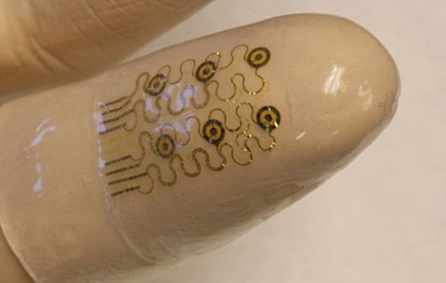
A developed a new “robotic skins” technology that allows users to turn
everyday objects into robots as well as help astronauts for Mars
exploration where the environment is unpredictable.
The skins,
developed and designed by researchers at the Yale University in
partnership with NASA, could be used for everything from
search-and-rescue robots to animate the inanimate everyday objects to
wearable technologies.The technology can also be reused to help astronauts accomplish an array of tasks with the same reconfigurable material.
The same skins used to make a robotic arm out of a piece of foam could be removed and applied to create a soft Mars rover that can roll over rough terrain.
With the robotic skins on board, anything from balloons to balls of crumpled paper could potentially be made into a robot with a purpose.
“One of the main things I considered was the importance of multifunctionality, especially for deep space exploration where the environment is unpredictable .
The skins are made from elastic sheets embedded with sensors and actuators. They are placed on a deformable object — a stuffed animal or a foam tube, for instance — then the skins animate these objects from their surfaces.
The makeshift robots can perform different tasks depending on the properties of the soft objects and how the skins are applied.
“We can take the skins and wrap them around one object to perform a task — locomotion, for example — and then take them off and put them on a different object to perform a different task, such as grasping and moving an object .
“We can then take those same skins off that object and put them on a shirt to make an active wearable device,”.
To demonstrate the robotic skins in action, the team created a handful of prototypes. These include foam cylinders that move like an inchworm, a shirt-like wearable device designed to correct poor posture, and a device with a gripper that can grasp and move objects

_______________________________________________________________________________
An upper-body exoskeleton that elevates and supports a worker’s arms to
assist them with chest-height and overhead tasks, the EksoVest is made
of lightweight materials, including carbon fiber mesh and a metal-tube
frame.
Wearable devices bestow incredible abilities, enable warehouse workers to lift great weights, gain extraordinary endurance and allow the disabled to recover some of their lost capabilities. These devices, called exoskeletons (exos) work with the user, augmenting, reinforcing and restoring human performance. Exos can consist of rigid materials, like steel, and soft parts such as elastic fabric. These devices can be active—powered by actuators and batteries—or passive, they can be mobile or stationary, and cover the entire body or just a single body segment.
The relationship between exos and the human body—with all of the operating variables and the need for seamless interplay—poses great challenges for design engineers. Additional complexities compound these difficulties, forcing development teams to face issues like usability, affordability and design flexibility.
These challenges are, to an extent, simply reflections of the technology’s evolution. Exos represent different things to different users and industries, and the technology’s complexity precludes a single clear definition. The fact is that exokeleton technology is continuously evolving and reinventing itself.
Forces Driving Exo Momentum
Many factors are promoting increased exo adoption. For example, startups have significantly enhanced these systems by improving drives, materials and power sub-systems. New battery technology now promises to power exo-suits for as long as eight hours.Furthermore, overall market conditions are improving. Changes in government policies have created an increasingly friendly regulatory environment. Equally important, the aging workforce and systemic skills shortage in developed countries has put pressure on companies to invest more in their employees, with exos becoming a force-multiplier to improve productivity.
As appealing as these benefits are, in this age of growing automation why deploy exos when you can use robots?
The answer is that the industrial sector isn’t ready to take humans out of its operations. Although exos enable humans to more efficiently perform physical tasks in industrial environments, humans provide an ingredient that current machine technology cannot match: agile intelligence. Industrial processes are often just too complex to automate with current systems.
This is where exo technology comes into play. Exos can act as a bridge between the extremes of fully manual, nontechnology-enabled tasks and those processes that demand traditional industrial robots. The exo-human hybrid provides a solution that leverages the intelligence of human operators and the strength, precision and endurance of machines.