Electronic switching system
In telecommunications, an electronic switching system (ESS) is a telephone switch that uses digital electronics and computerized control to interconnect telephone circuits for the purpose of establishing telephone calls.
The generations of telephone switches before the advent of electronic switching in the 1950s used purely electro-mechanical relay systems and analog voice paths. These early machines typically utilized the step-by-step technique. The first generation of electronic switching systems in the 1960s were not entirely digital in nature, but used reed relay-operated metallic paths or crossbar switches operated by stored program control (SPC) systems.
First announced in 1955, the first customer trial installation of an all-electronic central office commenced in Morris, Illinois in November 1960 by Bell Laboratories.[1] The first prominent large-scale electronic switching system was the Number One Electronic Switching System (1ESS) of the Bell System in the United States, introduced in Succasunna, New Jersey, in May 1965.
Later electronic switching systems implemented the digital representation of the electrical audio signals on subscriber loops by digitizing the analog signals and processing the resulting data for transmission between central offices. Time-division multiplexing (TDM) technology permitted the simultaneous transmission of multiple telephone calls on a single wire connection between central offices or other electronic switches, resulting in dramatic capacity improvements of the telephone network.
With the advances of digital electronics starting in the 1960s telephone switches employed semiconductor device components in increasing measure.
In the late 20th century most telephone exchanges without TDM processing were eliminated and the term electronic switching system became largely a historical distinction for the older SPC systems.
Transistor as a Switch
When used as an AC signal amplifier, the transistors Base biasing voltage is applied in such a way that it always operates within its “active” region, that is the linear part of the output characteristics curves are used.
However, both the NPN & PNP type bipolar transistors can be made to operate as “ON/OFF” type solid state switch by biasing the transistors Base terminal differently to that for a signal amplifier.
Solid state switches are one of the main applications for the use of transistor to switch a DC output “ON” or “OFF”. Some output devices, such as LED’s only require a few milliamps at logic level DC voltages and can therefore be driven directly by the output of a logic gate. However, high power devices such as motors, solenoids or lamps, often require more power than that supplied by an ordinary logic gate so transistor switches are used.
If the circuit uses the Bipolar Transistor as a Switch, then the biasing of the transistor, either NPN or PNP is arranged to operate the transistor at both sides of the “ I-V ” characteristics curves we have seen previously.
The areas of operation for a transistor switch are known as the Saturation Region and the Cut-off Region. This means then that we can ignore the operating Q-point biasing and voltage divider circuitry required for amplification, and use the transistor as a switch by driving it back and forth between its “fully-OFF” (cut-off) and “fully-ON” (saturation) regions as shown below.
Operating Regions

The pink shaded area at the bottom of the curves represents the “Cut-off” region while the blue area to the left represents the “Saturation” region of the transistor. Both these transistor regions are defined as:
1. Cut-off Region
Here the operating conditions of the transistor are zero input base current ( IB ), zero output collector current ( IC ) and maximum collector voltage ( VCE ) which results in a large depletion layer and no current flowing through the device. Therefore the transistor is switched “Fully-OFF”.
Cut-off Characteristics
 |
|
Then we can define the “cut-off region” or “OFF mode” when using a bipolar transistor as a switch as being, both junctions reverse biased, VB < 0.7v and IC = 0. For a PNP transistor, the Emitter potential must be negative with respect to the Base.
2. Saturation Region
Here the transistor will be biased so that the maximum amount of base current is applied, resulting in maximum collector current resulting in the minimum collector emitter voltage drop which results in the depletion layer being as small as possible and maximum current flowing through the transistor. Therefore the transistor is switched “Fully-ON”.
Saturation Characteristics
 |
|
Then we can define the “saturation region” or “ON mode” when using a bipolar transistor as a switch as being, both junctions forward biased, VB > 0.7v and IC = Maximum. For a PNP transistor, the Emitter potential must be positive with respect to the Base.
Then the transistor operates as a “single-pole single-throw” (SPST) solid state switch. With a zero signal applied to the Base of the transistor it turns “OFF” acting like an open switch and zero collector current flows. With a positive signal applied to the Base of the transistor it turns “ON” acting like a closed switch and maximum circuit current flows through the device.
The simplest way to switch moderate to high amounts of power is to use the transistor with an open-collector output and the transistors Emitter terminal connected directly to ground. When used in this way, the transistors open collector output can thus “sink” an externally supplied voltage to ground thereby controlling any connected load.
An example of an NPN Transistor as a switch being used to operate a relay is given below. With inductive loads such as relays or solenoids a flywheel diode is placed across the load to dissipate the back EMF generated by the inductive load when the transistor switches “OFF” and so protect the transistor from damage. If the load is of a very high current or voltage nature, such as motors, heaters etc, then the load current can be controlled via a suitable relay as shown.
Basic NPN Transistor Switching Circuit

The circuit resembles that of the Common Emitter circuit we looked at in the previous tutorials. The difference this time is that to operate the transistor as a switch the transistor needs to be turned either fully “OFF” (cut-off) or fully “ON” (saturated). An ideal transistor switch would have infinite circuit resistance between the Collector and Emitter when turned “fully-OFF” resulting in zero current flowing through it and zero resistance between the Collector and Emitter when turned “fully-ON”, resulting in maximum current flow.
In practice when the transistor is turned “OFF”, small leakage currents flow through the transistor and when fully “ON” the device has a low resistance value causing a small saturation voltage ( VCE ) across it. Even though the transistor is not a perfect switch, in both the cut-off and saturation regions the power dissipated by the transistor is at its minimum.
In order for the Base current to flow, the Base input terminal must be made more positive than the Emitter by increasing it above the 0.7 volts needed for a silicon device. By varying this Base-Emitter voltage VBE, the Base current is also altered and which in turn controls the amount of Collector current flowing through the transistor as previously discussed.
When maximum Collector current flows the transistor is said to be Saturated. The value of the Base resistor determines how much input voltage is required and corresponding Base current to switch the transistor fully “ON”.
Transistor as a Switch Example No1
Using the transistor values from the previous tutorials of: β = 200, Ic = 4mA and Ib = 20uA, find the value of the Base resistor (Rb) required to switch the load fully “ON” when the input terminal voltage exceeds 2.5v.

The next lowest preferred value is: 82kΩ, this guarantees the transistor switch is always saturated.
Transistor as a Switch Example No2
Again using the same values, find the minimum Base current required to turn the transistor “fully-ON” (saturated) for a load that requires 200mA of current when the input voltage is increased to 5.0V. Also calculate the new value of Rb.
Transistor Base current:

Transistor Base resistance:

Transistor switches are used for a wide variety of applications such as interfacing large current or high voltage devices like motors, relays or lamps to low voltage digital IC’s or logic gates like AND gates or OR gates. Here, the output from a digital logic gate is only +5v but the device to be controlled may require a 12 or even 24 volts supply. Or the load such as a DC Motor may need to have its speed controlled using a series of pulses (Pulse Width Modulation). transistor switches will allow us to do this faster and more easily than with conventional mechanical switches.
Digital Logic Transistor Switch

The base resistor, Rb is required to limit the output current from the logic gate.
PNP Transistor Switch
We can also use the PNP Transistors as a switch, the difference this time is that the load is connected to ground (0v) and the PNP transistor switches the power to it. To turn the PNP transistor operating as a switch “ON”, the Base terminal is connected to ground or zero volts (LOW) as shown.
PNP Transistor Switching Circuit

The equations for calculating the Base resistance, Collector current and voltages are exactly the same as for the previous NPN transistor switch. The difference this time is that we are switching power with a PNP transistor (sourcing current) instead of switching ground with an NPN transistor (sinking current).
Darlington Transistor Switch
Sometimes the DC current gain of the bipolar transistor is too low to directly switch the load current or voltage, so multiple switching transistors are used. Here, one small input transistor is used to switch “ON” or “OFF” a much larger current handling output transistor. To maximise the signal gain, the two transistors are connected in a “Complementary Gain Compounding Configuration” or what is more commonly called a “Darlington Configuration” were the amplification factor is the product of the two individual transistors.
Darlington Transistors simply contain two individual bipolar NPN or PNP type transistors connected together so that the current gain of the first transistor is multiplied with that of the current gain of the second transistor to produce a device which acts like a single transistor with a very high current gain for a much smaller Base current. The overall current gain Beta (β) or hfe value of a Darlington device is the product of the two individual gains of the transistors and is given as:
So Darlington Transistors with very high β values and high Collector currents are possible compared to a single transistor switch. For example, if the first input transistor has a current gain of 100 and the second switching transistor has a current gain of 50 then the total current gain will be 100 * 50 = 5000. So for example, if our load current from above is 200mA, then the darlington base current is only 200mA/5000 = 40uA. A huge reduction from the previous 1mA for a single transistor.
An example of the two basic types of Darlington transistor configurations are given below.
Darlington Transistor Configurations

The above NPN Darlington transistor switch configuration shows the Collectors of the two transistors connected together with the Emitter of the first transistor connected to the Base terminal of the second transistor therefore, the Emitter current of the first transistor becomes the Base current of the second transistor switching it “ON”.
The first or “input” transistor receives the input signal to its Base. This transistor amplifies it in the usual way and uses it to drive the second larger “output” transistors. The second transistor amplifies the signal again resulting in a very high current gain. One of the main characteristics of Darlington Transistors is their high current gains compared to single bipolar transistors.
As well as its high increased current and voltage switching capabilities, another advantage of a “Darlington Transistor Switch” is in its high switching speeds making them ideal for use in inverter circuits, lighting circuits and DC motor or stepper motor control applications.
One difference to consider when using Darlington transistors over the conventional single bipolar types when using the transistor as a switch is that the Base-Emitter input voltage ( VBE ) needs to be higher at approx 1.4v for silicon devices, due to the series connection of the two PN junctions.
Transistor as a Switch Summary
Then to summarise when using a Transistor as a Switch the following conditions apply:
- Transistor switches can be used to switch and control lamps, relays or even motors.
- When using the bipolar transistor as a switch they must be either “fully-OFF” or “fully-ON”.
- Transistors that are fully “ON” are said to be in their Saturation region.
- Transistors that are fully “OFF” are said to be in their Cut-off region.
- When using the transistor as a switch, a small Base current controls a much larger Collector load current.
- When using transistors to switch inductive loads such as relays and solenoids, a “Flywheel Diode” is used.
- When large currents or voltages need to be controlled, Darlington Transistors can be used.
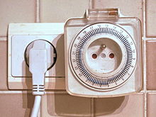
Time switch
A time switch (also called a timer switch, or simply timer) is a timer that operates an electric switch controlled by the timing mechanism.
The switch may be connected to an electric circuit operating from mains power, including via a relay or contactor; or low voltage, including battery-operated equipment in vehicles. It may be built into power circuits (as with a central heating or water heater timer), plugged into a wall outlet with equipment plugged into the timer instead of directly into the power point; or built into equipment as, for example, a sleep timer that turns off a television receiver after a set period.
The mechanism may be mechanical (e.g., clockwork; rarely used nowadays), electromechanical (e.g., a slowly rotating geared motor that mechanically operates switches) or electronic, with semiconductor timing circuitry and switching devices and no moving parts.
The timer may switch equipment on, off, or both, at a preset time or times, after a preset interval, or cyclically. A countdown time switch switches power, usually off, after a preset time. A cyclical timer switches equipment both on and off at preset times over a period, then repeats the cycle; the period is usually 24 hours or 7 days.
For example, a central heating timer may supply heat for a specified period during the morning and evening every weekday, and all day on weekends. A timer for an unattended slow cooker may switch on automatically at a time and for a period suitable to have food ready at mealtime. Likewise, a coffee maker may turn itself on early in the morning in time for awakening residents to have fresh coffee already brewed for them.
Timers may do other processing or have sensors; for example, a timer may switch on lights only during hours of darkness, using a seasonal algorithm[1] or light sensor. Combining the two allows a light to come on at sundown and go off at midnight, for example.
An astronomical (or astronomic) timer calculates dawn and dusk times for each day of the year based on the latitude and longitude (or just north/central/south and time zone on more cheaply made ones), and the day of the year (month and date), programmed by the user upon installation in addition to the usual time of day. This eliminates the need for a photocell (which may be repeatedly triggered on and off by the light which it operates) or for repeatedly re-setting a regular timer for seasonal changes in the length of day or for daylight-saving time. This allows exterior lighting like a porch light fixture to be controlled by simply replacing its indoor wall switch, or doing the same for a lamp in a dark interior corner (away from a window) by simply plugging-in a self-adjusting lamp timer.
Time switches can be used for many purposes, including saving electric energy by consuming it only when required, switching equipment on, off, or both at times required by some process, and home security (for example switching lights in a pattern that gives the impression that premises are attended) to reduce the likelihood of burglary or prowling.
Among applications are lighting (interior, exterior, and street lighting), cooking devices such as ovens, washing machines, and heating and cooling of buildings and vehicles.[2] Built-in automatic washing machine controllers are examples of very complex electromechanical and electronic timers cycles, starting and stopping many processes including pumps and valves to fill and empty the drum with water, heating, and rotating at different speeds, with different combinations of settings for different fabrics.


Solid-state electronics
Solid-state electronics means semiconductor electronics; electronic equipment using semiconductor devices such as semiconductor diodes, transistors, and integrated circuits (ICs).[1][2][3][4][5] The term is also used for devices in which semiconductor electronics which have no moving parts replace devices with moving parts, such as the solid-state relay in which transistor switches are used in place of a moving-arm electromechanical relay, or the solid state disk (SSD) a type of semiconductor memory used in computers to replace hard disk drives, which store data on a rotating disk.[6]
The term "solid state" became popular in the beginning of the semiconductor era in the 1960s to distinguish this new technology based on the transistor, in which the electronic action of devices occurred in a solid state, from previous electronic equipment that used vacuum tubes, in which the electronic action occurred in a gaseous state. A semiconductor device works by controlling an electric current consisting of electrons or holes moving within a solid crystalline piece of semiconducting material such as silicon, while the thermionic vacuum tubes it replaced worked by controlling current conducted by a gas of particles, electrons or ions, moving in a vacuum within a sealed tube. Although the first solid state electronic device was the cat's whisker detector, a crude semiconductor diode invented around 1904, solid state electronics really started with the invention of the transistor in 1947.[7] Before that, all electronic equipment used vacuum tubes, because vacuum tubes were the only electronic components which could amplify, an essential capability in all electronics. The replacement of bulky, fragile, energy-wasting vacuum tubes with transistors in the 1960s-70s created a revolution not just in technology but in people's habits, making possible the first truly portable consumer electronics such as the transistor radio, cassette tape player, walkie-talkie and quartz watch, as well as the first practical computers and mobile phones.
Today almost all electronics is solid state, except in some applications such as radio transmitters in which vacuum tubes are still used, and some power industrial control circuits which use electro mechanical devices such as relays. Additional examples of solid state electronic devices are the microprocessor chip, LED lamp, solar cell, charge coupled device (CCD) image sensor used in cameras, and semiconductor laser.

Time-division multiplexing (TDM) is a method of transmitting and receiving independent signals over a common signal path by means of synchronized switches at each end of the transmission line so that each signal appears on the line only a fraction of time in an alternating pattern. It is used when the bit rate of the transmission medium exceeds that of the signal to be transmitted. This form of signal multiplexing was developed in telecommunications for telegraphy systems in the late 19th century, but found its most common application in digital telephony in the second half of the 20th century.
XXX . XXX Multiplexing
In telecommunications and computer networks, multiplexing (sometimes contracted to muxing) is a method by which multiple analog or digital signals are combined into one signal over a shared medium. The aim is to share a scarce resource. For example, in telecommunications, several telephone calls may be carried using one wire. Multiplexing originated in telegraphy in the 1870s, and is now widely applied in communications. In telephony, George Owen Squier is credited with the development of telephone carrier multiplexing in 1910.
The multiplexed signal is transmitted over a communication channel such as a cable. The multiplexing divides the capacity of the communication channel into several logical channels, one for each message signal or data stream to be transferred. A reverse process, known as demultiplexing, extracts the original channels on the receiver end.
A device that performs the multiplexing is called a multiplexer (MUX), and a device that performs the reverse process is called a demultiplexer (DEMUX or DMX).
Inverse multiplexing (IMUX) has the opposite aim as multiplexing, namely to break one data stream into several streams, transfer them simultaneously over several communication channels, and recreate the original data stream.

Multiple variable bit rate digital bit streams may be transferred efficiently over a single fixed bandwidth channel by means of statistical multiplexing. This is an asynchronous mode time-domain multiplexing which is a form of time-division multiplexing.
Digital bit streams can be transferred over an analog channel by means of code-division multiplexing techniques such as frequency-hopping spread spectrum (FHSS) and direct-sequence spread spectrum (DSSS).
In wireless communications, multiplexing can also be accomplished through alternating polarization (horizontal/vertical or clockwise/counterclockwise) on each adjacent channel and satellite, or through phased multi-antenna array combined with a multiple-input multiple-output communications (MIMO) scheme.
Space-division multiplexing
In wired communication, space-division multiplexing, also known as Space-division multiple access is the use of separate point-to-point electrical conductors for each transmitted channel. Examples include an analogue stereo audio cable, with one pair of wires for the left channel and another for the right channel, and a multi-pair telephone cable, a switched star network such as a telephone access network, a switched Ethernet network, and a mesh network.
In wireless communication, space-division multiplexing is achieved with multiple antenna elements forming a phased array antenna. Examples are multiple-input and multiple-output (MIMO), single-input and multiple-output (SIMO) and multiple-input and single-output (MISO) multiplexing. An IEEE 802.11n wireless router with k antennas makes it in principle possible to communicate with k multiplexed channels, each with a peak bit rate of 54 Mbit/s, thus increasing the total peak bit rate by the factor k. Different antennas would give different multi-path propagation (echo) signatures, making it possible for digital signal processing techniques to separate different signals from each other. These techniques may also be utilized for space diversity (improved robustness to fading) or beamforming (improved selectivity) rather than multiplexing
Frequency-division multiplexing

Frequency-division multiplexing (FDM) is inherently an analog technology. FDM achieves the combining of several signals into one medium by sending signals in several distinct frequency ranges over a single medium. In FDM the signals are electrical signals. One of the most common applications for FDM is traditional radio and television broadcasting from terrestrial, mobile or satellite stations, or cable television. Only one cable reaches a customer's residential area, but the service provider can send multiple television channels or signals simultaneously over that cable to all subscribers without interference. Receivers must tune to the appropriate frequency (channel) to access the desired signal.[1]
A variant technology, called wavelength-division multiplexing (WDM) is used in optical communications.
Time-division multiplexing

Time-division multiplexing (TDM) is a digital (or in rare cases, analog) technology which uses time, instead of space or frequency, to separate the different data streams. TDM involves sequencing groups of a few bits or bytes from each individual input stream, one after the other, and in such a way that they can be associated with the appropriate receiver. If done sufficiently quickly, the receiving devices will not detect that some of the circuit time was used to serve another logical communication path.
Consider an application requiring four terminals at an airport to reach a central computer. Each terminal communicated at 2400 baud, so rather than acquire four individual circuits to carry such a low-speed transmission, the airline has installed a pair of multiplexers. A pair of 9600 baud modems and one dedicated analog communications circuit from the airport ticket desk back to the airline data center are also installed.[1] Some web proxy servers (e.g. polipo) use TDM in HTTP pipelining of multiple HTTP transactions onto the same TCP/IP connection.
Carrier sense multiple access and multidrop communication methods are similar to time-division multiplexing in that multiple data streams are separated by time on the same medium, but because the signals have separate origins instead of being combined into a single signal, are best viewed as channel access methods, rather than a form of multiplexing.
Polarization-division multiplexing
Polarization-division multiplexing uses the polarization of electromagnetic radiation to separate orthogonal channels. It is in practical use in both radio and optical communications, particularly in 100 Gbit/s per channel fiber optic transmission systems.
Orbital angular momentum multiplexing
Orbital angular momentum multiplexing is a relatively new and experimental technique for multiplexing multiple channels of signals carried using electromagnetic radiation over a single path. It can potentially be used in addition to other physical multiplexing methods to greatly expand the transmission capacity of such systems. As of 2012 it is still in its early research phase, with small-scale laboratory demonstrations of bandwidths of up to 2.5 Tbit/s over a single light path. This is a controversial subject in the academic community, with many claiming it is not a new method of multiplexing, but rather a special case of space-division multiplexing.
Code-division multiplexing
Code division multiplexing (CDM), Code division multiple access (CDMA) or spread spectrum is a class of techniques where several channels simultaneously share the same frequency spectrum, and this spectral bandwidth is much higher than the bit rate or symbol rate. One form is frequency hopping, another is direct sequence spread spectrum. In the latter case, each channel transmits its bits as a coded channel-specific sequence of pulses called chips. Number of chips per bit, or chips per symbol, is the spreading factor. This coded transmission typically is accomplished by transmitting a unique time-dependent series of short pulses, which are placed within chip times within the larger bit time. All channels, each with a different code, can be transmitted on the same fiber or radio channel or other medium, and asynchronously demultiplexed. Advantages over conventional techniques are that variable bandwidth is possible (just as in statistical multiplexing), that the wide bandwidth allows poor signal-to-noise ratio according to Shannon-Hartley theorem, and that multi-path propagation in wireless communication can be combated by rake receivers.
A significant application of CDMA is the Global Positioning System (GPS).

Multiple access method
A multiplexing technique may be further extended into a multiple access method or channel access method, for example, TDM into time-division multiple access (TDMA) and statistical multiplexing into carrier-sense multiple access (CSMA). A multiple access method makes it possible for several transmitters connected to the same physical medium to share its capacity.
Multiplexing is provided by the Physical Layer of the OSI model, while multiple access also involves a media access control protocol, which is part of the Data Link Layer.
The Transport layer in the OSI model, as well as TCP/IP model, provides statistical multiplexing of several application layer data flows to/from the same computer.
Code-division multiplexing (CDM) is a technique in which each channel transmits its bits as a coded channel-specific sequence of pulses. This coded transmission typically is accomplished by transmitting a unique time-dependent series of short pulses, which are placed within chip times within the larger bit time. All channels, each with a different code, can be transmitted on the same fiber and asynchronously demultiplexed. Other widely used multiple access techniques are time-division multiple access (TDMA) and frequency-division multiple access (FDMA). Code-division multiplex techniques are used as an access technology, namely code-division multiple access (CDMA), in Universal Mobile Telecommunications System (UMTS) standard for the third-generation (3G) mobile communication identified by the ITU.
Application areas
Telegraphy
The earliest communication technology using electrical wires, and therefore sharing an interest in the economies afforded by multiplexing, was the electric telegraph. Early experiments allowed two separate messages to travel in opposite directions simultaneously, first using an electric battery at both ends, then at only one end.
- Émile Baudot developed a time-multiplexing system of multiple Hughes machines in the 1870s.
- In 1874, the quadruplex telegraph developed by Thomas Edison transmitted two messages in each direction simultaneously, for a total of four messages transiting the same wire at the same time.
- Several workers were investigating acoustic telegraphy, a frequency-division multiplexing technique, which led to the invention of the telephone.
Telephony
In telephony, a customer's telephone line now typically ends at the remote concentrator box, where it is multiplexed along with other telephone lines for that neighborhood or other similar area. The multiplexed signal is then carried to the central switching office on significantly fewer wires and for much further distances than a customer's line can practically go. This is likewise also true for digital subscriber lines (DSL).
Fiber in the loop (FITL) is a common method of multiplexing, which uses optical fiber as the backbone. It not only connects POTS phone lines with the rest of the PSTN, but also replaces DSL by connecting directly to Ethernet wired into the home. Asynchronous Transfer Mode is often the communications protocol used.
Because all the phone (and data) lines have been clumped together, none of them can be accessed except through a demultiplexer. Where such demultiplexers are uncommon, this provides for more-secure communications, though the connections are not typically encrypted.
Cable TV has long carried multiplexed television channels, and late in the 20th century began offering the same services as telephone companies. IPTV also depends on multiplexing.
Video processing
In video editing and processing systems, multiplexing refers to the process of interleaving audio and video into one coherent data stream.
In digital video, such a transport stream is normally a feature of a container format which may include metadata and other information, such as subtitles. The audio and video streams may have variable bit rate. Software that produces such a transport stream and/or container is commonly called a statistical multiplexer or muxer. A demuxer is software that extracts or otherwise makes available for separate processing the components of such a stream or container.
Digital broadcasting
In digital television and digital radio systems, several variable bit-rate data streams are multiplexed together to a fixed bitrate transport stream by means of statistical multiplexing. This makes it possible to transfer several video and audio channels simultaneously over the same frequency channel, together with various services.
In the digital television systems, this may involve several standard definition television (SDTV) programmes (particularly on DVB-T, DVB-S2, ISDB and ATSC-C), or one HDTV, possibly with a single SDTV companion channel over one 6 to 8 MHz-wide TV channel. The device that accomplishes this is called a statistical multiplexer. In several of these systems, the multiplexing results in an MPEG transport stream. The newer DVB standards DVB-S2 and DVB-T2 has the capacity to carry several HDTV channels in one multiplex. Even the original DVB standards can carry more HDTV channels in a multiplex if the most advanced MPEG-4 compressions hardware is used.
On communications satellites which carry broadcast television networks and radio networks, this is known as multiple channel per carrier or MCPC. Where multiplexing is not practical (such as where there are different sources using a single transponder), single channel per carrier mode is used.
Signal multiplexing of satellite TV and radio channels is typically carried out in a central signal playout and uplink centre, such as SES Platform Services in Germany, which provides playout, digital archiving, encryption, and satellite uplinks, as well as multiplexing, for hundreds of digital TV and radio channels.
In digital radio, both the Digital Audio Broadcasting (DAB) Eureka 147 system of digital audio broadcasting and the in-band on-channel HD Radio, FMeXtra, and Digital Radio Mondiale systems can multiplex channels. This is essentially required with DAB-type transmissions (where a multiplex is called a DAB ensemble), but is entirely optional with IBOC systems.
Analog broadcasting
In FM broadcasting and other analog radio media, multiplexing is a term commonly given to the process of adding subcarriers to the audio signal before it enters the transmitter, where modulation occurs. (In fact, the stereo multiplex signal can be generated using time-division multiplexing, by switching between the two (left channel and right channel) input signals at an ultrasonic rate (the subcarrier), and then filtering out the higher harmonics.) Multiplexing in this sense is sometimes known as MPX, which in turn is also an old term for stereophonic FM, seen on stereo systems since the 1960s.
Other meanings
In spectroscopy the term is used to indicate that the experiment is performed with a mixture of frequencies at once and their respective response unravelled afterwards using the Fourier transform principle.
In computer programming, it may refer to using a single in-memory resource (such as a file handle) to handle multiple external resources (such as on-disk files).[6]
Some electrical multiplexing techniques do not require a physical "multiplexer" device, they refer to a "keyboard matrix" or "Charlieplexing" design style:
- Multiplexing may refer to the design of a multiplexed display (non-multiplexed displays are immune to break up).
- Multiplexing may refer to the design of a "switch matrix" (non-multiplexed buttons are immune to "phantom keys" and also immune to "phantom key blocking").
In high-throughput DNA sequencing, the term is used to indicate that some artificial sequences (often called barcodes or indexes) have been added to link given sequence reads to a given sample, and thus allow for the sequencing of multiple samples in the same reaction.
Electronic Switching System (ESS)
In an electronic switching system, control of switching functions are programmatically added to the memory and the related actions are run with help of the controlling processor. There are mainly two types of electronic switching systems: centralized stored program control and distributed stored program control. In centralized stored program control, a single processor is used for the exchange functionality. In distributed stored program control, there is no single or central processor for the overall function. It rather makes use of a small number of processors to perform the task.
Electronic switching systems make use of the concepts of the electronic data processor and operate with the help of high-speed switching networks and under the instructions from a stored-control program. The stored-control program controls the sequencing and call routing of operations for creating a call in the electronic switching system.
Before the advent of electronic switching, manual switching was used in telephone switches. The first generation of electronic switching systems, in the 1950s, used reed relay-operated metallic paths operated with the help of stored-program control systems. The later generation of electronic switching systems digitized analog signals and processed the resulting output for transmission between the central offices. The time-division-multiplexing technology allowed significant capacity improvements for the telephone network. The Number One Electronic Switching system of the Bell system was the first large-scale electronic switching system and was introduced in Succasunna, New Jersey, Unites States in 1965.
Manual switching had the big disadvantages of limited lifetime as well as slow operational speed for the electro mechanical component. These were overcome with the advent of the electronic switching system .
MOSFET as a Switch
We saw previously, that the N-channel, Enhancement-mode MOSFET (e-MOSFET) operates using a positive input voltage and has an extremely high input resistance (almost infinite) making it possible to interface with nearly any logic gate or driver capable of producing a positive output.
We also saw that due to this very high input (Gate) resistance we can safely parallel together many different MOSFETS until we achieve the current handling capacity that we required.
While connecting together various MOSFETS in parallel may enable us to switch high currents or high voltage loads, doing so becomes expensive and impractical in both components and circuit board space. To overcome this problem Power Field Effect Transistors or Power FET’s where developed.V
We now know that there are two main differences between field effect transistors, depletion-mode only for JFET’s and both enhancement-mode and depletion-mode for MOSFETs. In this tutorial we will look at using the Enhancement-mode MOSFET as a Switchas these transistors require a positive gate voltage to turn “ON” and a zero voltage to turn “OFF” making them easily understood as switches and also easy to interface with logic gates.
The operation of the enhancement-mode MOSFET, or e-MOSFET, can best be described using its I-V characteristics curves shown below. When the input voltage, ( VIN ) to the gate of the transistor is zero, the MOSFET conducts virtually no current and the output voltage ( VOUT ) is equal to the supply voltage VDD. So the MOSFET is “OFF” operating within its “cut-off” region.
MOSFET Characteristics Curves

The minimum ON-state gate voltage required to ensure that the MOSFET remains “ON” when carrying the selected drain current can be determined from the V-I transfer curves above. When VIN is HIGH or equal to VDD, the MOSFET Q-point moves to point A along the load line.
The drain current ID increases to its maximum value due to a reduction in the channel resistance. ID becomes a constant value independent of VDD, and is dependent only on VGS. Therefore, the transistor behaves like a closed switch but the channel ON-resistance does not reduce fully to zero due to its RDS(on) value, but gets very small.
Likewise, when VIN is LOW or reduced to zero, the MOSFET Q-point moves from point A to point B along the load line. The channel resistance is very high so the transistor acts like an open circuit and no current flows through the channel. So if the gate voltage of the MOSFET toggles between two values, HIGH and LOW the MOSFET will behave as a “single-pole single-throw” (SPST) solid state switch and this action is defined as:
1. Cut-off Region
Here the operating conditions of the transistor are zero input gate voltage ( VIN ), zero drain current ID and output voltage VDS = VDD. Therefore for an enhancement type MOSFET the conductive channel is closed and the device is switched “OFF”.
Cut-off Characteristics
 |
|
Then we can define the cut-off region or “OFF mode” when using an e-MOSFET as a switch as being, gate voltage, VGS < VTH and ID = 0. For a P-channel enhancement MOSFET, the Gate potential must be more positive with respect to the Source.
2. Saturation Region
In the saturation or linear region, the transistor will be biased so that the maximum amount of gate voltage is applied to the device which results in the channel resistance RDS(on being as small as possible with maximum drain current flowing through the MOSFET switch. Therefore for the enhancement type MOSFET the conductive channel is open and the device is switched “ON”.
Saturation Characteristics
 |
|
Then we can define the saturation region or “ON mode” when using an e-MOSFET as a switch as gate-source voltage, VGS > VTH and ID = Maximum. For a P-channel enhancement MOSFET, the Gate potential must be more negative with respect to the Source.
By applying a suitable drive voltage to the gate of an FET, the resistance of the drain-source channel, RDS(on) can be varied from an “OFF-resistance” of many hundreds of kΩ, effectively an open circuit, to an “ON-resistance” of less than 1Ω, effectively acting as a short circuit.
When using the MOSFET as a switch we can drive the MOSFET to turn “ON” faster or slower, or pass high or low currents. This ability to turn the power MOSFET “ON” and “OFF” allows the device to be used as a very efficient switch with switching speeds much faster than standard bipolar junction transistors.
An example of using the MOSFET as a switch

In this circuit arrangement an Enhancement-mode N-channel MOSFET is being used to switch a simple lamp “ON” and “OFF” (could also be an LED).
The gate input voltage VGS is taken to an appropriate positive voltage level to turn the device and therefore the lamp load either “ON”, ( VGS = +ve ) or at a zero voltage level that turns the device “OFF”, ( VGS = 0V ).
If the resistive load of the lamp was to be replaced by an inductive load such as a coil, solenoid or relay a “flywheel diode” would be required in parallel with the load to protect the MOSFET from any self generated back-emf.
Above shows a very simple circuit for switching a resistive load such as a lamp or LED. But when using power MOSFETs to switch either inductive or capacitive loads some form of protection is required to prevent the MOSFET device from becoming damaged. Driving an inductive load has the opposite effect from driving a capacitive load.
For example, a capacitor without an electrical charge is a short circuit, resulting in a high “inrush” of current and when we remove the voltage from an inductive load we have a large reverse voltage build up as the magnetic field collapses, resulting in an induced back-emf in the windings of the inductor.
Then we can summarise the switching characteristics of both the N-channel and P-channel type MOSFET within the following table.
| MOSFET Type | VGS (+ve) | VGS (0V) | VGS (-ve) |
| N-channel Enhancement | ON | OFF | OFF |
| N-channel Depletion | ON | ON | OFF |
| P-channel Enhancement | OFF | OFF | ON |
| P-channel Depletion | OFF | ON | ON |
Note that unlike the N-channel MOSFET whose gate terminal must be made more positive (attracting electrons) than the source to allow current to flow through the channel, the conduction through the P-channel MOSFET is due to the flow of holes. That is the gate terminal of a P-channel MOSFET must be made more negative than the source and will only stop conducting (cut-off) until the gate is more positive than the source.
So for the enhancement type power MOSFET to operate as an analogue switching device, it needs to be switched between its “Cut-off Region” where: VGS = 0V (or VGS = -ve) and its “Saturation Region” where: VGS(on) = +ve. The power dissipated in the MOSFET ( PD ) depends upon the current flowing through the channel ID at saturation and also the “ON-resistance” of the channel given as RDS(on). For example.
MOSFET as a Switch Example No1
Lets assume that the lamp is rated at 6v, 24W and is fully “ON”, the standard MOSFET has a channel on-resistance ( RDS(on) ) value of 0.1ohms. Calculate the power dissipated in the MOSFET switching device.
The current flowing through the lamp is calculated as:

Then the power dissipated in the MOSFET will be given as:

You may be sat there thinking, well so what!, but when using the MOSFET as a switch to control DC motors or electrical loads with high inrush currents the “ON” Channel resistance ( RDS(on) ) between the drain and the source is very important. For example, MOSFETs that control DC motors, are subjected to a high in-rush current when the motor first begins to rotate, because the motors starting current is only limited by the very low resistance value of the motors windings.
As the basic power relationship is: P = I2R, then a high RDS(on) channel resistance value would simply result in large amounts of power being dissipated and wasted within the MOSFET itself resulting in an excessive temperature rise, which if not controlled could result in the MOSFET becoming very hot and damaged due to a thermal overload.
A lower RDS(on) value for the channel resistance is also a desirable parameter as it helps to reduce the channels effective saturation voltage ( VDS(sat) = ID*RDS(on) ) across the MOSFET and will therefore operate at a cooler temperature. Power MOSFETs generally have a RDS(on) value of less than 0.01Ω which allows them to run cooler, extending their operational life span.
One of the main limitations when using a MOSFET as a switching device is the maximum drain current it can handle. So the RDS(on) parameter is an important guide to the switching efficiency of the MOSFET and is simply given as the ratio of VDS / ID when the transistor is switched “ON”.
When using a MOSFET or any type of field effect transistor for that matter as a solid-state switching device it is always advisable to select ones that have a very low RDS(on) value or at least mount them onto a suitable heatsink to help reduce any thermal runaway and damage. Power MOSFETs used as a switch generally have surge-current protection built into their design, but for high-current applications the bipolar junction transistor is a better choice.
Power MOSFET Motor Control
Because of the extremely high input or gate resistance that the MOSFET has, its very fast switching speeds and the ease at which they can be driven makes them ideal to interface with op-amps or standard logic gates. However, care must be taken to ensure that the gate-source input voltage is correctly chosen because when using the MOSFET as a switch the device must obtain a low RDS(on) channel resistance in proportion to this input gate voltage.
Low threshold type power MOSFETs may not switch “ON” until a least 3V or 4V has been applied to its gate and if the output from the logic gate is only +5V logic it may be insufficient to fully drive the MOSFET into saturation. Using lower threshold MOSFETs designed for interfacing with TTL and CMOS logic gates that have thresholds as low as 1.5V to 2.0V are available.
Power MOSFETs can be used to control the movement of DC motors or brushless stepper motors directly from computer logic or by using pulse-width modulation (PWM) type controllers. As a DC motor offers high starting torque and which is also proportional to the armature current, MOSFET switches along with a PWM can be used as a very good speed controller that would provide smooth and quiet motor operation.
Simple Power MOSFET Motor Controller

As the motor load is inductive, a simple flywheel diode is connected across the inductive load to dissipate any back emf generated by the motor when the MOSFET turns it “OFF”. A clamping network formed by a zener diode in series with the diode can also be used to allow for faster switching and better control of the peak reverse voltage and drop-out time.
For added security an additional silicon or zener diode D1 can also be placed across the channel of a MOSFET switch when using inductive loads, such as motors, relays, solenoids, etc, for suppressing over voltage switching transients and noise giving extra protection to the MOSFET switch if required. Resistor RGS is used as a pull-down resistor to help pull the TTL output voltage down to 0V when the MOSFET is switched “OFF”.
P-channel MOSFET Switch
Thus far we have looked at the N-channel MOSFET as a switch were the MOSFET is placed between the load and the ground. This also allows for the MOSFET’s gate drive or switching signal to be referenced to ground (low-side switching).

P-channel
MOSFET Switch
MOSFET Switch
But in some applications we require the use of P-channel enhancement-mode MOSFET were the load is connected directly to ground. In this instance the MOSFET switch is connected between the load and the positive supply rail (high-side switching) as we do with PNP transistors.
In a P-channel device the conventional flow of drain current is in the negative direction so a negative gate-source voltage is applied to switch the transistor “ON”.
This is achieved because the P-channel MOSFET is “upside down” with its source terminal tied to the positive supply +VDD. Then when the switch goes LOW, the MOSFET turns “ON” and when the switch goes HIGH the MOSFET turns “OFF”.
This upside down connection of a P-channel enhancement mode MOSFET switch allows us to connect it in series with a N-channel enhancement mode MOSFET to produce a complementary or CMOS switching device as shown across a dual supply.
Complementary MOSFET Motor Controller

The two MOSFETs are configured to produce a bi-directional switch from a dual supply with the motor connected between the common drain connection and ground reference. When the input is LOW the P-channel MOSFET is switched-ON as its gate-source junction is negatively biased so the motor rotates in one direction. Only the positive +VDDsupply rail is used to drive the motor.
When the input is HIGH, the P-channel device switches-OFF and the N-channel device switches-ON as its gate-source junction is positively biased. The motor now rotates in the opposite direction because the motors terminal voltage has been reversed as it is now supplied by the negative -VDD supply rail.
Then the P-channel MOSFET is used to switch the positive supply to the motor for forward direction (high-side switching) while the N-channel MOSFET is used to switch the negative supply to the motor for reverse direction (low-side switching).
There are a variety of configurations for driving the two MOSFETs with many different applications. Both the P-channel and the N-channel devices can be driven by a single gate drive IC as shown.
However, to avoid cross conduction with both MOSFETS conducting at the same time across the two polarities of the dual supply, fast switching devices are required to provide some time difference between them turning “OFF” and the other turning “ON”. One way to overcome this problem is to drive both MOSFETS gates separately. This then produces a third option of “STOP” to the motor when both MOSFETS are “OFF”.
Complementary MOSFET Motor Control Table
| MOSFET 1 | MOSFET 2 | Motor Function |
| OFF | OFF | Motor Stopped (OFF) |
| ON | OFF | Motor Rotates Forward |
| OFF | ON | Motor Rotates Reverse |
| ON | ON | NOT ALLOWED |
Please note it is important that there are no other combination of inputs allowed at the same time as this may cause the power supply to become shorted out, as both MOSFETS, FET1 and FET2 could be switched “ON” together resulting in: ( fuse = bang! ), be warned.
Relay Switch Circuit
The advantage of relays is that it takes a relatively small amount of power to operate the relay coil, but the relay itself can be used to control motors, heaters, lamps or AC circuits which themselves can draw a lot more electrical power.
The electro-mechanical relay is an output device (actuator) which come in a whole host of shapes, sizes and designs, and have many uses and applications in electronic circuits. But while electrical relays can be used to allow low power electronic or computer type circuits to switch relatively high currents or voltages both “ON” or “OFF”, some form of relay switch circuit is required to control it.
The design and types of relay switching circuits is huge, but many small electronic projects use transistors and MOSFETs as their main switching device as the transistor can provide fast DC switching (ON-OFF) control of the relay coil from a variety of input sources so here is a small collection of some of the more common ways of switching relays.
NPN Relay Switch Circuit
A typical relay switch circuit has the coil driven by a NPN transistor switch, TR1 as shown depending on the input voltage level. When the Base voltage of the transistor is zero (or negative), the transistor is cut-off and acts as an open switch. In this condition no Collector current flows and the relay coil is de-energised because being current devices, if no current flows into the Base, then no current will flow through the relay coil.
If a large enough positive current is now driven into the Base to saturate the NPN transistor, the current flowing from Base to Emitter (B to E) controls the larger relay coil current flowing through the transistor from the Collector to Emitter.
For most bipolar switching transistors, the amount of relay coil current flowing into the Collector would be somewhere between 50 to 800 times that of the required Base current to drive the transistor into saturation. The current gain, or beta value ( β ) of the general purpose BC109 shown is typically about 290 at 2mA (Datasheet).
NPN Relay Switch Circuit

Note that the relay coil is not only an electromagnet but it is also an inductor. When power is applied to the coil due to the switching action of the transistor, a maximum current will flow as a result of the DC resistance of the coil as defined by Ohms Law, (I = V/R). Some of this electrical energy is stored within the relay coil’s magnetic field.
When the transistor switches “OFF”, the current flowing through the relay coil decreases and the magnetic field collapses. However the stored energy within the magnetic field has to go some where and a reverse voltage is developed across the coil as it tries to maintain the current in the relay coil. This action produces a high voltage spike across the relays coil that can damage the switching NPN transistor if allowed to build up.
So in order to prevent damage to the semiconductor transistor, a “flywheel diode”, also known as a freewheeling diode, is connected across the relay coil. This flywheel diode clamps the reverse voltage across the coil to about 0.7V dissipating the stored energy and protecting the switching transistor. Flywheel diodes are only applicable when the supply is a polarized DC voltage. An AC coil requires a different protection method, and for this an RC snubber circuit is used.
NPN Darlington Relay Switch Circuit
The previous NPN transistor relay switch circuit is ideal for switching small loads such as LED’s and miniature relays. But sometimes it is required to switch larger relay coils or currents beyond the range of a BC109 general purpose transistor and this can be achieved using Darlington Transistors.
The sensitivity and current gain of a relay switch circuit can be greatly increased by using a Darlington pair of transistors in place of a single switching transistor. Darlington Transistor pairs can be made from two individually connected Bipolar Transistors as shown or available as one single device with standard: Base, Emitter and Collector connecting leads.
The two NPN transistors are connected as shown so that the Collector current of the first transistor, TR1 becomes the Base current of the second transistor TR2. The application of a positive base current to TR1 automatically turns “ON” the switching transistor, TR2.
NPN Darlington Relay Switch Circuit

If two individual transistors are configured as a Darlington switching pair, then a small value resistor (100 to 1,000Ω’s) is usually placed between the Base and Emitter of the main switching transistor, TR2 to ensure that it turns fully OFF. Again a flywheel diode is used to protect TR2 from the back emf generated when the relay coil is de-energised.
Emitter Follower Relay Switch Circuit
As well as the standard Common Emitter configuration for a relay switch circuit, the relay coil can also be connected to the Emitter terminal of the transistor to form an Emitter Follower circuit. The input signal is connected directly to the Base, while the output is taken from the Emitter load as shown.
Emitter Follower Relay Switch Circuit

The Common Collector, or Emitter Follower configuration is very useful for impedance matching applications because of the very high input impedance, in the region of hundreds of thousands of Ohms while having a relatively low output impedance to switch the relays coil. As with the previous NPN relay switch circuit, switching occurs by applying a positive current to the base of the transistor.
Emitter Darlington Relay Switch Circuit
This is the Darlington transistor version of the previous Emitter Follower circuit. A very small positive Base current applied to TR1 causes a much greater Collector current to flow through TR2 due to the multiplication of the two Beta values.
Emitter Darlington Relay Switch Circuit

The Common Emitter Darlington relay switch circuit is useful to provide current gain and power gain with the voltage gain approximately equal to unity. Another important characteristic of this type of Emitter Follower circuit is that it has a high input impedance and a low output impedance, which make it ideal for impedance matching to large relay coils.
PNP Relay Switch Circuit
As well as switching relay coils and other such loads with NPN Bipolar Transistors, we can also switch them using PNP Bipolar Transistors. The PNP relay switch circuit is no different to the NPN relay switching circuit in terms of its ability to control the relays coil. However, it does require different polarities of operating voltages. For example, the Collector-Emitter voltage, Vce , must be negative for the PNP type to cause current flow from the Emitter to the Collector.
PNP Relay Switch Circuit

The PNP transistor circuit works in opposite to the NPN relay switching circuit. Load current flows from the Emitter to the Collector when the Base is forward biased with a voltage that is more negative than that at the Emitter. For the relays load current to flow through the Emitter to the Collector, both the Base and the Collector must be negative in respect to the Emitter.
In other words, when Vin is HIGH the PNP transistor is switched “OFF” and so too is the relay coil. When Vin is LOW, the Base voltage is less than the Emitter voltage, (more negative) and the PNP transistor turns “ON”. The Base resistor value sets the Base current, which sets the Collector current that drives the relay coil.
PNP transistor switches can be used when the switching signal is the reverse for an NPN transistor, for example the output of a CMOS NAND gate or other such logic device. A CMOS logic output has the drive strength at logic 0 to sink sufficient current to turn the PNP transistor “ON”. Then current sinks can be turned into current sources by using PNP transistors and a power supply of opposite polarity.
PNP Collector Relay Switch Circuit
The operation of this circuit is the same as the previous relay switching circuit. In this relay switch circuit, the relay load has been connected to the PNP transistors Collector. The ON-OFF switching action of the transistor and coil occurs when Vin is LOW, transistor “ON” and when Vin is HIGH, transistor “OFF”.
PNP Collector Relay Switch Circuit

We have seen that either an NPN bipolar transistor or an PNP bipolar transistor can operate as a switch for relay switching, or any other load for that matter. But that there are two different conditions that need to be understood as the current flows in two different directions.
So in an NPN transistor, a HIGH voltage with respect to the Emitter is applied to the Base, current flows from the Collector to the Emitter and the NPN transistor switches “ON”. For a PNP transistor, a LOW voltage with respect to the Emitter is applied to the Base, current flows from the Emitter to the Collector and the PNP transistor switches “ON”.
N-channel MOSFET Relay Switch Circuit
MOSFET relay switching operation is very similar to Bipolar Junction Transistor (BJT) switch operation seen above, and any of the previous circuits can be implemented using MOSFETs. However, there are some major differences in the operation of the MOSFET circuits with the main ones being that MOSFETs are voltage operated devices, and as the Gate is electrically isolated from the Drain-Source channel, they have very high input impedances so the Gate current for a MOSFET is zero, therefore a base resistor is unnecessary.
MOSFETs conduct through a conductive channel with the channel initially being closed, transistor “OFF”. This channel gradually increasing in conductive width as the voltage applied to the Gate terminal is slowly increased. In other words, the transistor operates by enhancing the channel as the Gate voltage increases and for this reason the this type of MOSFET is called an Enhancement MOSFET, or E-MOSFET.
N-channel Enhancement MOSFETs (NMOS) are the most commonly used type of MOSFET as a positive voltage on the Gate terminal switches the MOSFET “ON” and zero or a negative voltage on the Gate switches it “OFF”, making ideal as MOSFET relay switch. Complementary P-channel Enhancement MOSFETs are also available which, like the PNP BJT work with opposite voltages.
N-channel MOSFET Relay Switch Circuit

The above MOSFET relay switch circuit is connected in a common-source configuration. With zero voltage input, LOW condition, the value of VGS, there is insufficient Gate drive to open the channel and the transistor is “OFF”. But when VGS is increased above the MOSFETs lower threshold voltage VT, the channel opens, current flows and the relay coil is operated.
Then the enhancement mode MOSFET operates as a normally open switch making it ideal for switching small loads such as relays. E-type MOSFETs have high “OFF” resistance but moderate “ON” resistance (OK for most applications), so when selecting one for a particular switching application, its RDS value needs to be taken into consideration.
P-channel MOSFET Relay Switch Circuit
The P-channel Enhancement MOSFET (PMOS) is constructed the same as for the N-channel Enhancement MOSFET except that it operates with negative Gate voltages only. In other words, A P-channel MOSFET operates in the same fashion but with opposite polarities as the Gate must be more negative than the Source to turn “ON” the transistor by being forward-biased as shown.
P-channel MOSFET Relay Switch Circuit

In this configuration, the P-channels Source terminal is connected to +Vdd and the Drain terminal is connected to ground via the relays coil. When a HIGH voltage level is applied to the Gate, the P-channel MOSFET will be turned “OFF”. The turned “OFF” E-MOSFET will have a very high channel resistance and acts nearly like an open circuit.
When a LOW voltage level is applied to the Gate, the P-channel MOSFET will be turned “ON”. This will cause current to flow through the low resistance path of e-MOSFETs channel operating the relay coil. Both N-channel and P-channel e-MOSFETs make excellent low voltage relay switching circuits and can easily be interfaced to a wide variety of digital logic gates and micro-processor applications.
Logic Controlled Relay Switch Circuit
The N-channel, enhancement-type MOSFET is extremely useful as a transistor switch because in its “OFF” state (with zero Gate bias) its channel has a very high resistance blocking current flow. However, a relatively small positive voltage greater than the threshold voltage VT, on its high impedance Gate causes it to begin conducting current from its Drain terminal to its Source terminal.
Unlike the Bipolar Junction Transistor which requires a Base current to turn it “ON”, the e-MOSFET only requires a voltage on the Gate as due to its insulated Gate construction, zero current flows into the Gate. Then this makes the e-MOSFET, either N-channel or P-channel ideal to be driven directly by typical TTL or CMOS logic gates as shown.
Logic Controlled Relay Switch Circuit

Here the N-channel E-MOSFET is being driven by a digital logic gate. The output pins of most logic gates can only supply a limited amount of current, typically no more than about 20 mA. As e-MOSFETs are voltage operated devices and consume no Gate current, we can use a MOSFET relay switch circuit to control high power loads.
Micro-controller Relay Switch Circuit
As well as digital logic gates, we can also use the output pins and channels of micro-controllers, PIC’s and processors to control the outside world. The circuit below shows how to interface a relay using a MOSFET switch.
Micro-controller Relay Switch Circuit

Relay Switching Circuit Summary
In this tutorial we have seen how we can use both Bipolar Junction Transistors, either NPN or PNP and Enhancement MOSFETs, either N-channel or P-channel as a transistor switching circuit.
Sometimes when building Electronic or Micro-controller circuits we want to use a transistor switch to control a high-power device, such as motors, lamps, heating elements or AC circuits. Generally these devices require larger currents or higher voltages than a single power transistor can handle then we can use a relay switching circuit to do this.
Bipolar transistors (BJT’s) make very good and cheap relay switching circuits, but BJT’s are current operated devices as they convert a small Base current into a larger load current to energise the relay coil.
However, the MOSFET switch is ideal as an electrical switch as it takes virtually no Gate current to turn “ON”, converting a Gate voltage into a load current. Therefore, a MOSFET can be operated as a voltage-controlled switch.
In many applications bipolar transistors can be substituted with enhancement-type MOSFETs offering faster switching action, much higher input impedance, and probably less power dissipation. The combination of a very high Gate impedance, very low power consumption in its “OFF” state, and very fast switching capability makes the MOSFET suitable for many digital switching applications. Also with zero Gate current its switching action can not overload the output circuit of a digital gate or micro-controller.
However, because the gate of an E-MOSFET is insulated from the rest of the component, it is especially sensitive to static electricity which could destroy the thin oxide layer on the Gate. Then special care should be taken either when handling the component, or when it is in use and that any circuit using e-MOSFETs includes appropriate protection from static and voltage spikes.
Also for additional protection of either BJT’s or MOSFETs, always use a flywheel diode across and relay coil to safely dissipate the back emf generated by the transistors switching action.
Single-IC-based electronic circuit replaces mechanical switch
A simple and inexpensive electronic circuit uses a low-cost pushbutton switch to toggle the electrical power on and off. The circuit replaces a more costly and bulky push-push mechanical switch. The pushbutton switch triggers a monoshot circuit. The monoshot circuit’s output triggers a toggle flip-flop, which inverts its output state and controls power to the load.
Figure 1 A pair of flip-flops configured as a monoshot and a toggle flip-flop
debounce a simple, inexpensive push button switch.
Several implementations of the scheme are possible. Figure 1 shows a single-IC implementation. The circuit uses two flip-flops, IC1 and IC2, in the same IC, CD4027B. You configure IC1 as a monoshot circuit by feeding its output back to its reset pin through an RC network. IC1 outputs a high on the rising edge of the clock by tying its J input high and its K input low. The pushbutton switch connects between the clock input of IC1 and ground. The switch can also connect between the clock input and the positive supply, VDD. By tying IC2’s J and K inputs high, IC2becomes a toggle flip-flop. The output of IC1 clocks IC2 and toggles its output on the rising edge of the IC1 output.
Figure 2 Trace 1 is the voltage across the clock of IC1, Trace 2 is the output of
IC1, Trace 3 is the voltage on capacitor C1, and Trace 4 is the output of IC2
You can understand the operation of the circuit by observing the waveform at different points of the circuit (Figure 2). When you press the pushbutton switch, due to debouncing, IC1’s output goes high on the clock’s rising edge. Capacitor C1 starts charging through R1 toward high voltage. At the same instant, IC2 receives a rising-edge transition at its clock and toggles its output. When capacitor C1’s voltage exceeds the threshold of the IC1 reset pin, IC1 resets, and its output goes low. C1 now discharges through R1 to low voltage. The charging and discharging rate of C1 are equal. The duration of the monoshot circuit’s output pulse handles the switch-press time and the debouncing period. Varying the value of R1 varies the pulse period, and you can set R1 for different types of pushbutton switches. Complementary outputs of IC2 are available, and you can use them to drive power switches, such as transistors, MOSFETs, relays, and shutdown pins of switching regulators. The circuit operates over a supply voltage of 3 to 15V and can control power to analog and digital circuits
What are relays?
A relay is an electromagnetic switch operated by a relatively small electric current that can turn on or off a much larger electric current. The heart of a relay is an electromagnet (a coil of wire that becomes a temporary magnet when electricity flows through it). You can think of a relay as a kind of electric lever: switch it on with a tiny current and it switches on ("leverages") another appliance using a much bigger current. Why is that useful? As the name suggests, many sensors are incredibly sensitive pieces of electronic equipment and produce only small electric currents. But often we need them to drive bigger pieces of apparatus that use bigger currents. Relays bridge the gap, making it possible for small currents to activate larger ones. That means relays can work either as switches (turning things on and off) or as amplifiers (converting small currents into larger ones).
How relays work
Here are two simple animations illustrating how relays use one circuit to switch on a second circuit.
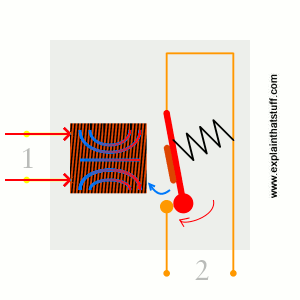
When power flows through the first circuit (1), it activates the electromagnet (brown), generating a magnetic field (blue) that attracts a contact (red) and activates the second circuit (2). When the power is switched off, a spring pulls the contact back up to its original position, switching the second circuit off again.
This is an example of a "normally open" (NO) relay: the contacts in the second circuit are not connected by default, and switch on only when a current flows through the magnet. Other relays are "normally closed" (NC; the contacts are connected so a current flows through them by default) and switch off only when the magnet is activated, pulling or pushing the contacts apart. Normally open relays are the most common.
Here's another animation showing how a relay links two circuits together. It's essentially the same thing drawn in a slightly different way. On the left side, there's an input circuit powered by a switch or a sensor of some kind. When this circuit is activated, it feeds current to an electromagnet that pulls a metal switch closed and activates the second, output circuit (on the right side). The relatively small current in the input circuit thus activates the larger current in the output circuit:
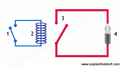
- The input circuit (black loop) is switched off and no current flows through it until something (either a sensor or a switch closing) turns it on. The output circuit (blue loop) is also switched off.
- When a small current flows in the input circuit, it activates the electromagnet (shown here as a red coil), which produces a magnetic field all around it.
- The energized electromagnet pulls the metal bar in the output circuit toward it, closing the switch and allowing a much bigger current to flow through the output circuit.
- The output circuit operates a high-current appliance such as a lamp or an electric motor.
Relays in practice

Photo: Another look at relays. Top: Looking straight down, you can see the spring contacts on the left, the switch mechanism in the middle, and the electromagnet coil on the right. Bottom: The same relay photographed from the front.
Suppose you want to build an electronically operated cooling system that switches a fan on or off as your room temperature changes. You could use some kind of electronic thermometer circuit to sense the temperature, but it would produce only small electric currents—far too tiny to power the electric motor in a great big fan. Instead, you could connect the thermometer circuit to the input circuit of a relay. When a small current flows in this circuit, the relay will activate its output circuit, allowing a much bigger current to flow and turning on the fan.
Who invented relays?
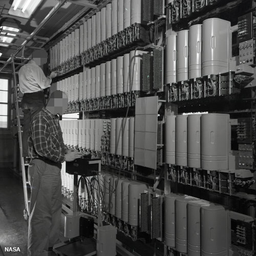
Photo: Relays were widely used for switching and routing calls in telephone exchanges such as this one, pictured in 1952.
Relays were invented in 1835 by American electromagnetism pioneer Joseph Henry; in a demonstration at the College of New Jersey, Henry used a small electromagnet to switch a larger one on and off, and speculated that relays could be used to control electrical machines over very long distances. Henry applied this idea to another invention he was working on at the time, the electric telegraph (the forerunner of the telephone), which was successfully developed by William Cooke and Charles Wheatstone in England and (much more famously) by Samuel F. B. Morse in the United States. Relays were later used in telephone switching and early electronic computers and remained hugely popular until transistors came along in the late 1940s; according to Bancroft Gherardi, marking the 100th anniversary of Henry's work on electromagnetism, there were an estimated 70 million relays in operation in the United States alone by that time. Transistors are tiny electronic components that can do a similar job to relays, working as either amplifiers or switches. Although they switch faster, use far less electricity, take up a fraction of the space, and cost much less than relays, they generally work with only tiny currents so relays are still used in many applications. It was the development of transistors that spurred on the computer revolution from the mid-20th century onward. But without relays, there would have been no transistors, so relays—and pioneers like Joseph Henry—deserve some of the credit too!
Types of Switches- Special Applications by Touch Control

Types of Switches- Special Applications by Touch Control
The switch is an electrical device that is used to break or make an electrical circuit manually or automatically. The working principle of switch depends on ON/ OFF mechanism. Various electrical or electronic circuits use switches to control or trigger the owl circuit. The types of switches depend on the connections of the circuit they make. Two essential components such as pole and through can confirm what types of connections a switch can make. These two components are also used to define variations of switch contact.
Here, the poles and throws can be defined as; when the number of circuits is controlled by a switch is called poles, whereas throws can be defined as the number of positions that the switch can adopt. A single throw switch consists one pair of contacts like open or close. A double throw switch includes a contact, which can be connected to two other contacts. When the switch is activated, then the current flows through between the two terminals of the switch. When the switch is OFF, then the current doesn’t flow between the two terminals of the switch.
Types of Switches
The types of switches are classified into four types namely:
- SPST (Single Pole Single through)
- SPDT (single pole double throw)
- DPST (double pole, single throw)
- DPDT (double pole double throw)

Types of Switches
SPST (Single Pole Single Through)
The SPST is a basic ON/OFF switch, that is used to connect or break the connection between two terminals. The power supply for the owl circuit is given by this switch. A simple PST switch is shown below.

SPST
The application of SPST switch is light switch given below and it is also called as a toggle switch. This type of switch has one input and one output. This light switch circuit controls one wire and makes one connection. This is an ON/OFF switch, when the switch in the below circuit is ON or closed, then the current flows through the two terminals and the bulb in the circuit will blink. When the switch is OFF or open, then the current doesn’t flow through the two terminals.

SPST-Circuit
SPDT (Single Pole Double Throw)
The SPDT switch is a three terminal switch, one terminal is used as input and remaining two terminals are used as outputs. It joins a mutual terminal to one or the other of two terminals.In the SPDT switch, instead of other terminals, just use COM terminal. For example, we can use COM & A or COM & B.

SPDT
The application of SPDT switch is mainly involved in a three-way circuit to turn ON/OFF a light from two locations like from the top & bottom of a stairway. In the circuit below, when the switch A is closed, then the current flows through the terminals, but only light A will glow and light B will OFF. When the switch B is closed, then the current flows through the terminals and only light B will glow and light ‘A’ will OFF. Her two circuits will be controlled through one source or one way.

SPDT-Circuit
DPST (Double Pole, Single Throw)
The DPST switch consists of two poles that means it includes two identical switches located on side by side. This switch is operated by one single toggle, which means that two discrete circuits are controlled at a time through one push.

DPST
This switch is used to turn two circuits ON/OFF and it consists of four terminals namely two inputs and two o/ps. The main purpose of this switch is to regulate a 240V appliance, where both supply voltages must be ON whereas the unbiased wire may be always connected. When this switch is ON then the current starts flowing through two circuits and when it is turned OFF then it is turned OFF.
DPDT (Double Pole Double Throw)
This switch is equal to two SPDT switches, it means two separate circuits, connecting two inputs of each circuit to one of two outputs. The switch position controls the number of ways and from the two contacts each contact can be routed.

DPDT
When it is in ON-ON mode or ON-OFF-ON mode they work like two discrete SPDT switches worked by the similar actuator. At a time only two loads can be ON. A DPDT switch can be used in any application that needs an open & closed wiring system.

DPDT-Circuit
The best example of this is, modeling of the railroad, that makes use of small scaled railways and trains, cars and bridges. The closed permits for the system to be switched at all times, whereas open permits for extra piece to be switched ON or triggered through the relay. From the following circuit, A, B and C connections from one pole of the switch and D, E and F connections from the other pole of the switch. Connections B and E are mutual in each of the poles.
If the +Vs enters at connection B & the switch is fixed to the top most position, then the connection A becomes +ve and the motor will rotate in one direction. If the switch is set to the lowest position, the power supply is inverted and connection D becomes +ve then the motor will rotate in the opposite direction. In the middle position, the power supply is not linked to the motor and it does not rotate. This kind of switch is mainly used in several motor controllers where speed of that motor is to be inverted.
Special Applications by Touch Control
Touch Controlled Load Switch
The main objective of this project is to design a touch controlled load switch. This project uses a 555 timer in monostable mode to drive a relay to turn ON a load for a fixed time duration.
Touch Controlled Load Switch Project
The 555 timer IC is activated by a touch plate attached to its trigger pin. The output of 555 delivers high for a fixed time interval as decided by the RC time constant connected to the timer.
This output drives a relay which in turn switches ON the load for that duration after which is turned OFF automatically. Human body induced mains supply advances a voltage on the touch plate to activate the timer.
Touch Controlled Musical Bell
This circuit generates a musical tone when somebody touches the touch panel in the circuit, This circuit uses two AA cells and produces plenty sound.
The proposed circuit uses an IC UM3481 which is used in musical circuits. This integrated circuit includes a ROM with 512 musical tones, tone generator, ROM with 512 musical notes, rhythm generator, runoff control, modulator, oscillators, pre-amplifiers and frequency divider.
Touch Controlled Load Switch Project Kit
To design this circuit a few of the basic components are required. In this circuit, R1 and C1 works as the timing components for the oscillator. The Q1 transistor is used for driving the loudspeaker. The base terminal of the Q2 transistor is used as the touch panel display to activate the musical bell.
Thus, this is all about types of switches and special applications with touch control. We hope that you have got a better understanding of this concept.Furthermore, any queries regarding this topic or applications of touch controlled switch projects please give your feedback by commenting in the comment section below. Here is a question for you, what are the some more applications of touch controlled switch?


++++++++++++++++++++++++++++++++++++++++++++++++++++++++++++++++++
Electronic Switching System = Trans I C
++++++++++++++++++++++++++++++++++++++++++++++++++++++++++++++++++
Really thanks for sharing this useful post !! This post is very informative about electronic switching system . keep sharing.
BalasHapusTechbasha