karnaugh map and combined and compared with KWH meter
karnaugh map is a method for solving problem problems in digital combination circuits and sequential circuits in digital, when digital concepts are applied in a series of electronics it is necessary to simplify the simplification of the concept of the whole circuit especially in consideration:
1. efficient use of components
2. ease in soldering component
3. the fewer components are used but the output of the circuit is the same
4. Performance tool more flexible
5. make it easy in trouble shooting circuit
6. More easily damped oscillation system
7. Comparison of output and input more can be defined
8. Allows controlling K W H meter with karnaugh ( Car Now Ugh ) map concept
( Allows Difference Application To Re Steady State )
XXX . XXX 4%zero Sum and Product Notation

Don’t Care Cells in the Karnaugh Map
Up to this point we have considered logic reduction problems where the input conditions were completely specified. That is, a 3-variable truth table or Karnaugh map had 2n = 23 or 8-entries, a full table or map. It is not always necessary to fill in the complete truth table for some real-world problems. We may have a choice to not fill in the complete table.
For example, when dealing with BCD (Binary Coded Decimal) numbers encoded as four bits, we may not care about any codes above the BCD range of (0, 1, 2…9). The 4-bit binary codes for the hexadecimal numbers (Ah, Bh, Ch, Eh, Fh) are not valid BCD codes. Thus, we do not have to fill in those codes at the end of a truth table, or K-map, if we do not care to. We would not normally care to fill in those codes because those codes (1010, 1011, 1100, 1101, 1110, 1111) will never exist as long as we are dealing only with BCD encoded numbers. These six invalid codes are don’t cares as far as we are concerned. That is, we do not care what output our logic circuit produces for these don’t cares.
Don’t cares in a Karnaugh map, or truth table, may be either 1s or 0s, as long as we don’t care what the output is for an input condition we never expect to see. We plot these cells with an asterisk, *, among the normal 1s and 0s. When forming groups of cells, treat the don’t care cell as either a 1 or a 0, or ignore the don’t cares. This is helpful if it allows us to form a larger group than would otherwise be possible without the don’t cares. There is no requirement to group all or any of the don’t cares. Only use them in a group if it simplifies the logic.

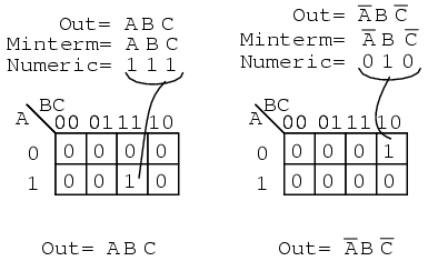
Above is an example of a logic function where the desired output is 1 for input ABC = 101 over the range from 000 to 101. We do not care what the output is for the other possible inputs (110, 111). Map those two as don’t cares. We show two solutions. The solution on the right Out = AB’C is the more complex solution since we did not use the don’t care cells. The solution in the middle, Out=AC, is less complex because we grouped a don’t care cell with the single 1 to form a group of two. The third solution, a Product-Of-Sums on the right, results from grouping a don’t care with three zeros forming a group of four 0s. This is the same, less complex, Out=AC. We have illustrated that the don’t care cells may be used as either 1s or 0s, whichever is useful.

The electronics class of Lightning State College has been asked to build the lamp logic for a stationary bicycle exhibit at the local science museum. As a rider increases his pedaling speed, lamps will light on a bar graph display. No lamps will light for no motion. As speed increases, the lower lamp, L1 lights, then L1 and L2, then, L1, L2, and L3, until all lamps light at the highest speed. Once all the lamps illuminate, no further increase in speed will have any effect on the display.
A small DC generator coupled to the bicycle tire outputs a voltage proportional to speed. It drives a tachometer board which limits the voltage at the high end of speed where all lamps light. No further increase in speed can increase the voltage beyond this level. This is crucial because the downstream A to D (Analog to Digital) converter puts out a 3-bit code, ABC, 23 or 8-codes, but we only have five lamps. A is the most significant bit, C the least significant bit.
The lamp logic needs to respond to the six codes out of the A to D. For ABC=000, no motion, no lamps light. For the five codes (001 to 101) lamps L1, L1&L2, L1&L2&L3, up to all lamps will light, as speed, voltage, and the A to D code (ABC) increases. We do not care about the response to input codes (110, 111) because these codes will never come out of the A to D due to the limiting in the tachometer block. We need to design five logic circuits to drive the five lamps.
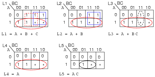
Since, none of the lamps light for ABC=000 out of the A to D, enter a 0 in all K-maps for cell ABC=000. Since we don’t care about the never to be encountered codes (110, 111), enter asterisks into those two cells in all five K-maps.
Lamp L5 will only light for code ABC=101. Enter a 1 in that cell and five 0s into the remaining empty cells of L5 K-map.
L4 will light initially for code ABC=100, and will remain illuminated for any code greater, ABC=101, because all lamps below L5 will light when L5 lights. Enter 1s into cells 100 and 101 of the L4 map so that it will light for those codes. Four 0‘s fill the remaining L4 cells
L3 will initially light for code ABC=011. It will also light whenever L5 and L4 illuminate. Enter three 1s into cells 011, 100, 101 for L3 map. Fill three 0s into the remaining L3 cells.
L2 lights for ABC=010 and codes greater. Fill 1s into cells 010, 011, 100, 101, and two 0s in the remaining cells.
The only time L1 is not lighted is for no motion. There is already a 0 in cell ABC=000. All the other five cells receive 1s.
Group the 1‘s as shown above, using don’t cares whenever a larger group results. The L1 map shows three product terms, corresponding to three groups of 4-cells. We used both don’t cares in two of the groups and one don’t care on the third group. The don’t cares allowed us to form groups of four.
In a similar manner, the L2 and L4 maps both produce groups of 4-cells with the aid of the don’t care cells. The L4 reduction is striking in that the L4 lamp is controlled by the most significant bit from the A to D converter, L5=A. No logic gates are required for lamp L4. In the L3 and L5 maps, single cells form groups of two with don’t care cells. In all five maps, the reduced Boolean equation is less complex than without the don’t cares.
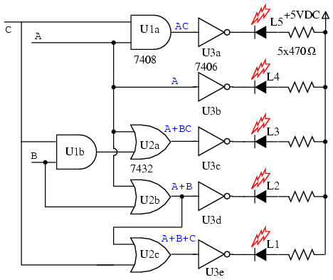
The gate diagram for the circuit is above. The outputs of the five K-map equations drive inverters. Note that the L1 OR gate is not a 3-input gate but a 2-input gate having inputs (A+B), C, outputting A+B+C The open collector inverters, 7406, are desirable for driving LEDs, though, not part of the K-map logic design. The output of an open collecter gate or inverter is open circuited at the collector internal to the integrated circuit package so that all collector current may flow through an external load. An active high into any of the inverters pulls the output low, drawing current through the LED and the current limiting resistor. The LEDs would likely be part of a solid state relay driving 120VAC lamps for a museum exhibit, not shown here.
Larger Karnaugh maps reduce larger logic designs. How large is large enough? That depends on the number of inputs, fan-ins, to the logic circuit under consideration. One of the large programmable logic companies has an answer.
Altera’s own data, extracted from its library of customer designs, supports the value of heterogeneity. By examining logic cones, mapping them onto LUT-based nodes and sorting them by the number of inputs that would be best at each node, Altera found that the distribution of fan-ins was nearly flat between two and six inputs, with a nice peak at five.
The answer is no more than six inputs for most all designs, and five inputs for the average logic design. The five variable Karnaugh map follows.
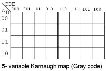
The older version of the five variable K-map, a Gray Code map or reflection map, is shown above. The top (and side for a 6-variable map) of the map is numbered in full Gray code. The Gray code reflects about the middle of the code. This style map is found in older texts. The newer preferred style is below.
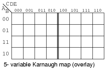
The overlay version of the Karnaugh map, shown above, is simply two (four for a 6-variable map) identical maps except for the most significant bit of the 3-bit address across the top. If we look at the top of the map, we will see that the numbering is different from the previous Gray code map. If we ignore the most significant digit of the 3-digit numbers, the sequence 00, 01, 11, 10 is at the heading of both sub maps of the overlay map. The sequence of eight 3-digit numbers is not Gray code. Though the sequence of four of the least significant two bits is.
Let’s put our 5-variable Karnaugh Map to use. Design a circuit which has a 5-bit binary input (A, B, C, D, E), with A being the MSB (Most Significant Bit). It must produce an output logic High for any prime number detected in the input data.
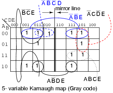
We show the solution above on the older Gray code (reflection) map for reference. The prime numbers are (1,2,3,5,7,11,13,17,19,23,29,31). Plot a 1 in each corresponding cell. Then, proceed with grouping of the cells. Finish by writing the simplified result. Note that 4-cell group A’B’E consists of two pairs of cell on both sides of the mirror line. The same is true of the 2-cell group AB’DE. It is a group of 2-cells by being reflected about the mirror line. When using this version of the K-map look for mirror images in the other half of the map.
Out = A’B’E + B’C’E + A’C’DE + A’CD’E + ABCE + AB’DE + A’B’C’D
Below we show the more common version of the 5-variable map, the overlay map.
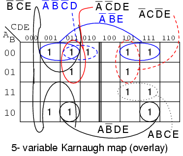
If we compare the patterns in the two maps, some of the cells in the right half of the map are moved around since the addressing across the top of the map is different. We also need to take a different approach at spotting commonality between the two halves of the map. Overlay one half of the map atop the other half. Any overlap from the top map to the lower map is a potential group. The figure below shows that group AB’DE is composed of two stacked cells. Group A’B’E consists of two stacked pairs of cells.
For the A’B’E group of 4-cells ABCDE = 00xx1 for the group. That is A,B,E are the same 001 respectively for the group. And, CD=xx that is it varies, no commonality in CD=xx for the group of 4-cells. Since ABCDE = 00xx1, the group of 4-cells is covered by A’B’XXE = A’B’E.
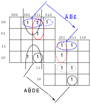
The above 5-variable overlay map is shown stacked.
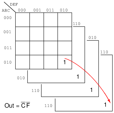
An example of a six variable Karnaugh map follows. We have mentally stacked the four sub maps to see the group of 4-cells corresponding to Out = C’F’
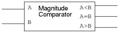
A magnitude comparator (used to illustrate a 6-variable K-map) compares two binary numbers, indicating if they are equal, greater than, or less than each other on three respective outputs. A three bit magnitude comparator has two inputs A2A1A0 and B2B1B0 An integrated circuit magnitude comparator (7485) would actually have four inputs, But, the Karnaugh map below needs to be kept to a reasonable size. We will only solve for the A>B output.
Below, a 6-variable Karnaugh map aids simplification of the logic for a 3-bit magnitude comparator. This is an overlay type of map. The binary address code across the top and down the left side of the map is not a full 3-bit Gray code. Though the 2-bit address codes of the four sub maps is Gray code. Find redundant expressions by stacking the four sub maps atop one another (shown above). There could be cells common to all four maps, though not in the example below. It does have cells common to pairs of sub maps.
The A>B output above is ABC>XYZ on the map below.
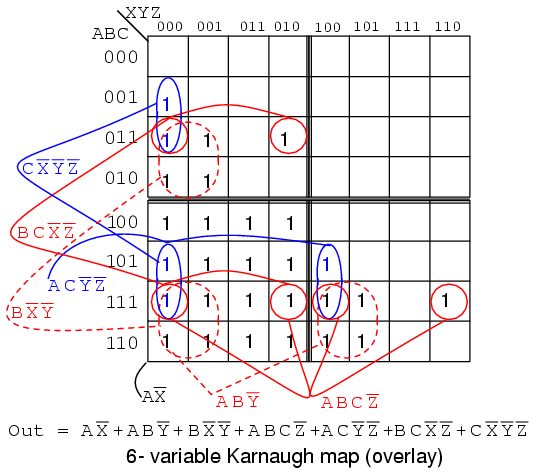
Where ever ABC is greater than XYZ, a 1 is plotted. In the first line ABC=000 cannot be greater than any of the values of XYZ. No 1s in this line. In the second line, ABC=001, only the first cell ABCXYZ= 001000 is ABC greater than XYZ. A single 1 is entered in the first cell of the second line. The fourth line, ABC=010, has a pair of 1s. The third line, ABC=011 has three 1s. Thus, the map is filled with 1s in any cells where ABC is greater than XXZ.
In grouping cells, form groups with adjacent sub maps if possible. All but one group of 16-cells involves cells from pairs of the sub maps. Look for the following groups:
- 1 group of 16-cells
- 2 groups of 8-cells
- 4 groups of 4-cells
The group of 16-cells, AX’ occupies all of the lower right sub map; though, we don’t circle it on the figure above.
One group of 8-cells is composed of a group of 4-cells in the upper sub map overlaying a similar group in the lower left map. The second group of 8-cells is composed of a similar group of 4-cells in the right sub map overlaying the same group of 4-cells in the lower left map.
The four groups of 4-cells are shown on the Karnaugh map above with the associated product terms. Along with the product terms for the two groups of 8-cells and the group of 16-cells, the final Sum-Of-Products reduction is shown, all seven terms. Counting the 1s in the map, there is a total of 16+6+6=28 ones. Before the K-map logic reduction there would have been 28 product terms in our SOP output, each with 6-inputs. The Karnaugh map yielded seven product terms of four or less inputs. This is really what Karnaugh maps are all about!
The wiring diagram is not shown. However, here is the parts list for the 3-bit magnitude comparator for ABC>XYZ using 4 TTL logic family parts:
- 1 ea 7410 triple 3-input NAND gate AX’, ABY’, BX’Y’
- 2 ea 7420 dual 4-input NAND gate ABCZ’, ACY’Z’, BCX’Z’, CX’Y’Z’
- 1 ea 7430 8-input NAND gate for output of 7-P-terms
- REVIEW:
- Boolean algebra, Karnaugh maps, and CAD (Computer Aided Design) are methods of logic simplification. The goal of logic simplification is a minimal cost solution.
- A minimal cost solution is a valid logic reduction with the minimum number of gates with the minimum number of inputs.
- Venn diagrams allow us to visualize Boolean expressions, easing the transition to Karnaugh maps.
- Karnaugh map cells are organized in Gray code order so that we may visualize redundancy in Boolean expressions which results in simplification.
- The more common Sum-Of-Products (Sum of Minters) expressions are implemented as AND gates (products) feeding a single OR gate (sum).
- Sum-Of-Products expressions (AND-OR logic) are equivalent to a NAND-NAND implementation. All AND gates and OR gates are replaced by NAND gates.
- Less often used, Product-Of-Sums expressions are implemented as OR gates (sums) feeding into a single AND gate (product). Product-Of-Sums expressions are based on the 0s, maxterms, in a Karnaugh map.
XXX . XXX 4%zero null 0 Karnaugh Maps - Rules of Simplification
The Karnaugh map uses the following rules for the simplification of expressions by grouping together adjacent cells containing ones
- Groups may not include any cell containing a zero

- Groups may be horizontal or vertical, but not diagonal.

- Groups must contain 1, 2, 4, 8, or in general 2n cells.
That is if n = 1, a group will contain two 1's since 21 = 2.
If n = 2, a group will contain four 1's since 22 = 4.
- Each group should be as large as possible.

- Each cell containing a one must be in at least one group.

- Groups may overlap.

- Groups may wrap around the table. The leftmost cell in a row may be grouped with the rightmost cell and the top cell in a column may be grouped with the bottom cell.

- There should be as few groups as possible, as long as this does not contradict any of the previous rules.

Summmary:
- No zeros allowed.
- No diagonals.
- Only power of 2 number of cells in each group.
- Groups should be as large as possible.
- Every one must be in at least one group.
- Overlapping allowed.
- Wrap around allowed.
- Fewest number of groups possible.
Minterm vs Maxterm Solution
So far we have been finding Sum-Of-Product (SOP) solutions to logic reduction problems. For each of these SOP solutions, there is also a Product-Of-Sums solution (POS), which could be more useful, depending on the application. Before working a Product-Of-Sums solution, we need to introduce some new terminology. The procedure below for mapping product terms is not new to this chapter. We just want to establish a formal procedure for minterms for comparison to the new procedure for maxterms.
A minterm is a Boolean expression resulting in 1 for the output of a single cell, and 0s for all other cells in a Karnaugh map, or truth table. If a minterm has a single 1 and the remaining cells as 0s, it would appear to cover a minimum area of 1s. The illustration above left shows the minterm ABC, a single product term, as a single 1 in a map that is otherwise 0s. We have not shown the 0s in our Karnaugh maps up to this point, as it is customary to omit them unless specifically needed. Another minterm A’BC’ is shown above right. The point to review is that the address of the cell corresponds directly to the minterm being mapped. That is, the cell 111 corresponds to the minterm ABC above left. Above right we see that the minterm A’BC’ corresponds directly to the cell 010. A Boolean expression or map may have multiple minterms.
Referring to the above figure, Let’s summarize the procedure for placing a minterm in a K-map:
- Identify the minterm (product term) term to be mapped.
- Write the corresponding binary numeric value.
- Use binary value as an address to place a 1 in the K-map
- Repeat steps for other minterms (P-terms within a Sum-Of-Products).
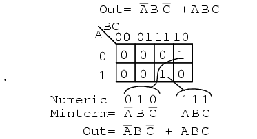
A Boolean expression will more often than not consist of multiple minterms corresponding to multiple cells in a Karnaugh map as shown above. The multiple minterms in this map are the individual minterms which we examined in the previous figure above. The point we review for reference is that the 1s come out of the K-map as a binary cell address which converts directly to one or more product terms. By directly we mean that a 0corresponds to a complemented variable, and a 1 corresponds to a true variable. Example: 010 converts directly to A’BC’. There was no reduction in this example. Though, we do have a Sum-Of-Products result from the minterms.
Referring to the above figure, Let’s summarize the procedure for writing the Sum-Of-Products reduced Boolean equation from a K-map:
- Form largest groups of 1s possible covering all minterms. Groups must be a power of 2.
- Write binary numeric value for groups.
- Convert binary value to a product term.
- Repeat steps for other groups. Each group yields a p-terms within a Sum-Of-Products.
Nothing new so far, a formal procedure has been written down for dealing with minterms. This serves as a pattern for dealing with maxterms.
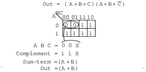
Next we attack the Boolean function which is 0 for a single cell and 1s for all others.
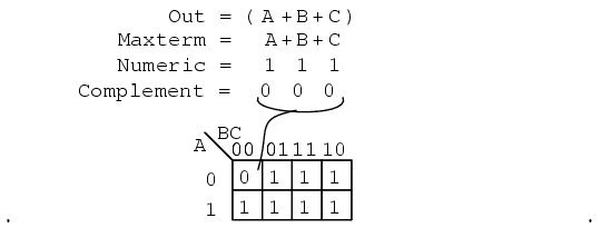
A maxterm is a Boolean expression resulting in a 0 for the output of a single cell expression, and 1s for all other cells in the Karnaugh map, or truth table. The illustration above left shows the maxterm (A+B+C), a single sum term, as a single 0 in a map that is otherwise 1s. If a maxterm has a single 0 and the remaining cells as 1s, it would appear to cover a maximum area of 1s.
There are some differences now that we are dealing with something new, maxterms. The maxterm is a 0, not a1 in the Karnaugh map. A maxterm is a sum term, (A+B+C) in our example, not a product term.
It also looks strange that (A+B+C) is mapped into the cell 000. For the equation Out=(A+B+C)=0, all three variables (A, B, C) must individually be equal to 0. Only (0+0+0)=0 will equal 0. Thus we place our sole 0 for minterm (A+B+C) in cell A,B,C=000 in the K-map, where the inputs are all0 . This is the only case which will give us a 0 for our maxterm. All other cells contain 1s because any input values other than ((0,0,0) for (A+B+C)yields 1s upon evaluation.
Referring to the above figure, the procedure for placing a maxterm in the K-map is:
- Identify the Sum term to be mapped.
- Write corresponding binary numeric value.
- Form the complement
- Use the complement as an address to place a 0 in the K-map
- Repeat for other maxterms (Sum terms within Product-of-Sums expression).
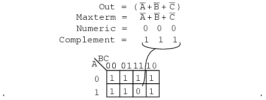
Another maxterm A’+B’+C’ is shown above. Numeric 000 corresponds to A’+B’+C’. The complement is 111. Place a 0 for maxterm (A’+B’+C’) in this cell (1,1,1) of the K-map as shown above.
Why should (A’+B’+C’) cause a 0 to be in cell 111? When A’+B’+C’ is (1’+1’+1’), all 1s in, which is (0+0+0)after taking complements, we have the only condition that will give us a 0. All the 1s are complemented to all 0s, which is 0 when ORed.
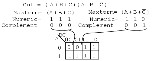
A Boolean Product-Of-Sums expression or map may have multiple maxterms as shown above. Maxterm(A+B+C) yields numeric 111 which complements to 000, placing a 0 in cell (0,0,0). Maxterm (A+B+C’) yields numeric 110 which complements to 001, placing a 0 in cell (0,0,1).
Now that we have the k-map setup, what we are really interested in is showing how to write a Product-Of-Sums reduction. Form the 0s into groups. That would be a group of two below. Write the binary value corresponding to the sum-term which is (0,0,X). Both A and B are 0 for the group. But, C is both 0 and 1 so we write an X as a place holder for C. Form the complement (1,1,X). Write the Sum-term (A+B) discarding the C and the X which held its’ place. In general, expect to have more sum-terms multiplied together in the Product-Of-Sums result. Though, we have a simple example here.
Let’s summarize the procedure for writing the Product-Of-Sums Boolean reduction for a K-map:
- Form largest groups of 0s possible, covering all maxterms. Groups must be a power of 2.
- Write binary numeric value for group.
- Complement binary numeric value for group.
- Convert complement value to a sum-term.
- Repeat steps for other groups. Each group yields a sum-term within a Product-Of-Sums result.
Example:
Simplify the Product-Of-Sums Boolean expression below, providing a result in POS form.

Solution:
Transfer the seven maxterms to the map below as 0s. Be sure to complement the input variables in finding the proper cell location.
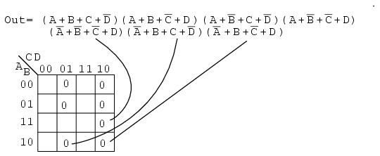
We map the 0s as they appear left to right top to bottom on the map above. We locate the last three maxterms with leader lines..
Once the cells are in place above, form groups of cells as shown below. Larger groups will give a sum-term with fewer inputs. Fewer groups will yield fewer sum-terms in the result.
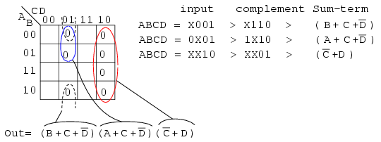
We have three groups, so we expect to have three sum-terms in our POS result above. The group of 4-cells yields a 2-variable sum-term. The two groups of 2-cells give us two 3-variable sum-terms. Details are shown for how we arrived at the Sum-terms above. For a group, write the binary group input address, then complement it, converting that to the Boolean sum-term. The final result is product of the three sums.
Example:
Simplify the Product-Of-Sums Boolean expression below, providing a result in SOP form.
Solution:
This looks like a repeat of the last problem. It is except that we ask for a Sum-Of-Products Solution instead of the Product-Of-Sums which we just finished. Map the maxterm 0s from the Product-Of-Sums given as in the previous problem, below left.
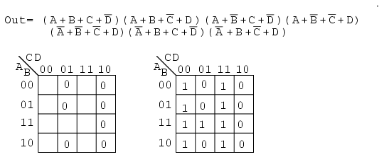
Then fill in the implied 1s in the remaining cells of the map above right.
Form groups of 1s to cover all 1s. Then write the Sum-Of-Products simplified result as in the previous section of this chapter. This is identical to a previous problem.
Above we show both the Product-Of-Sums solution, from the previous example, and the Sum-Of-Products solution from the current problem for comparison. Which is the simpler solution? The POS uses 3-OR gates and 1-AND gate, while the SOP uses 3-AND gates and 1-OR gate. Both use four gates each. Taking a closer look, we count the number of gate inputs. The POS uses 8-inputs; the SOP uses 7-inputs. By the definition of minimal cost solution, the SOP solution is simpler. This is an example of a technically correct answer that is of little use in the real world.
The better solution depends on complexity and the logic family being used. The SOP solution is usually better if using the TTL logic family, as NAND gates are the basic building block, which works well with SOP implementations. On the other hand, A POS solution would be acceptable when using the CMOS logic family since all sizes of NOR gates are available.
The gate diagrams for both cases are shown above, Product-Of-Sums left, and Sum-Of-Products right.
Below, we take a closer look at the Sum-Of-Products version of our example logic, which is repeated at left.
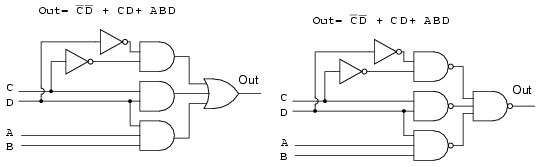
Above all AND gates at left have been replaced by NAND gates at right.. The OR gate at the output is replaced by a NAND gate. To prove that AND-OR logic is equivalent to NAND-NAND logic, move the inverter invert bubbles at the output of the 3-NAND gates to the input of the final NAND as shown in going from above right to below left.
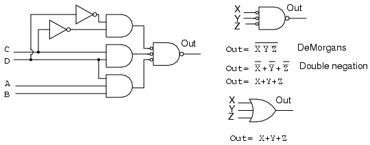
Above right we see that the output NAND gate with inverted inputs is logically equivalent to an OR gate by DeMorgan’s theorem and double negation. This information is useful in building digital logic in a laboratory setting where TTL logic family NAND gates are more readily available in a wide variety of configurations than other types.
The Procedure for constructing NAND-NAND logic, in place of AND-OR logic is as follows:
- Produce a reduced Sum-Of-Products logic design.
- When drawing the wiring diagram of the SOP, replace all gates (both AND and OR) with NAND gates.
- Unused inputs should be tied to logic High.
- In case of troubleshooting, internal nodes at the first level of NAND gate outputs do NOT match AND-OR diagram logic levels, but are inverted. Use the NAND-NAND logic diagram. Inputs and final output are identical, though.
- Label any multiple packages U1, U2,.. etc.
- Use data sheet to assign pin numbers to inputs and outputs of all gates.
Example:
Let us revisit a previous problem involving an SOP minimization. Produce a Product-Of-Sums solution. Compare the POS solution to the previous SOP.
Solution:
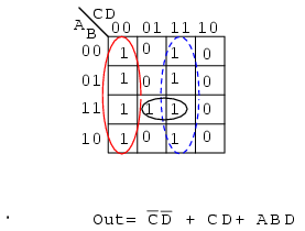
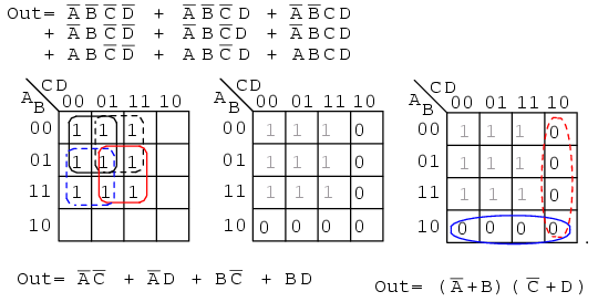
Above left we have the original problem starting with a 9-minterm Boolean unsimplified expression. Reviewing, we formed four groups of 4-cells to yield a 4-product-term SOP result, lower left.
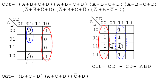
In the middle figure, above, we fill in the empty spaces with the implied 0s. The 0s form two groups of 4-cells. The solid blue group is (A’+B), the dashed red group is (C’+D). This yields two sum-terms in the Product-Of-Sums result, above right Out = (A’+B)(C’+D)
Comparing the previous SOP simplification, left, to the POS simplification, right, shows that the POS is the least cost solution. The SOP uses 5-gates total, the POS uses only 3-gates. This POS solution even looks attractive when using TTL logic due to simplicity of the result. We can find AND gates and an OR gate with 2-inputs.
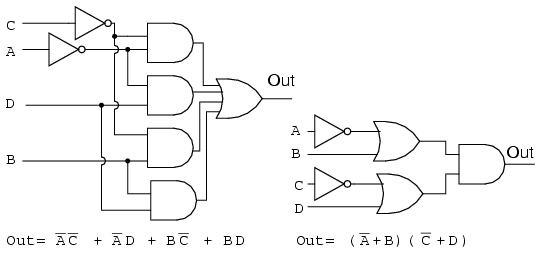
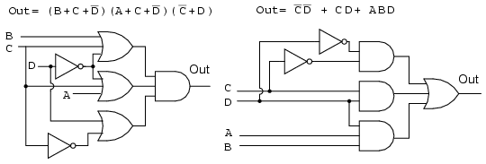
The SOP and POS gate diagrams are shown above for our comparison problem.
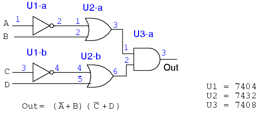
Given the pin-outs for the TTL logic family integrated circuit gates below, label the maxterm diagram above right with Circuit designators (U1-a, U1-b, U2-a, etc), and pin numbers.
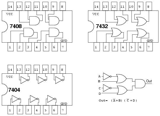
Each integrated circuit package that we use will receive a circuit designator: U1, U2, U3. To distinguish between the individual gates within the package, they are identified as a, b, c, d, etc. The 7404 hex-inverter package is U1. The individual inverters in it are are U1-a, U1-b, U1-c, etc. U2 is assigned to the 7432 quad OR gate. U3 is assigned to the 7408 quad AND gate. With reference to the pin numbers on the package diagram above, we assign pin numbers to all gate inputs and outputs on the schematic diagram below.
We can now build this circuit in a laboratory setting. Or, we could design a printed circuit board for it. A printed circuit board contains copper foil “wiring” backed by a non conductive substrate of phenolic, or epoxy-fiberglass. Printed circuit boards are used to mass produce electronic circuits. Ground the inputs of unused gates.
Label the previous POS solution diagram above left (third figure back) with Circuit designators and pin numbers. This will be similar to what we just did.
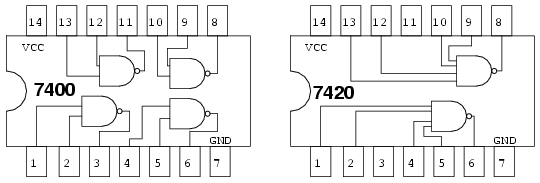
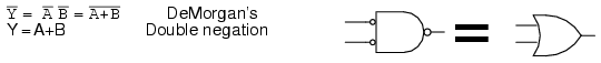
We can find 2-input AND gates, 7408 in the previous example. However, we have trouble finding a 4-input OR gate in our TTL catalog. The only kind of gate with 4-inputs is the 7420 NAND gate shown above right.
We can make the 4-input NAND gate into a 4-input OR gate by inverting the inputs to the NAND gate as shown below. So we will use the 7420 4-input NAND gate as an OR gate by inverting the inputs.
We will not use discrete inverters to invert the inputs to the 7420 4-input NAND gate, but will drive it with 2-input NAND gates in place of the AND gates called for in the SOP, minterm, solution. The inversion at the output of the 2-input NAND gates supply the inversion for the 4-input OR gate.
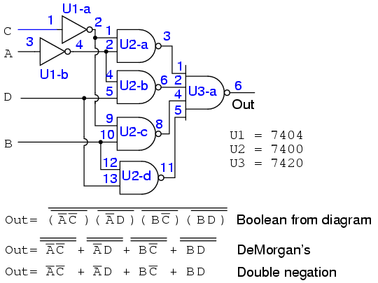
The result is shown above. It is the only practical way to actually build it with TTL gates by using NAND-NAND logic replacing AND-OR logic.
XXX . XXX 4%zero null 0 1 2 Synchronization
Synchronization is the coordination of events to operate asystem in unison. The conductor of an orchestra keeps the orchestra synchronized or in time. Systems that operate with all parts in synchrony are said to be synchronous or in sync—and those that are not are asynchronous.
Today, time synchronization can occur between systems around the world through satellite navigation signals.
The primary focus of this article is asynchronous control in digital electronic systems. In a synchronous system, operations (instructions, calculations, logic, etc.) are coordinated by one, or more, centralized clock signals. An asynchronous digital system, in contrast, has no global clock. Asynchronous systems do not depend on strict arrival times of signals or messages for reliable operation. Coordination is achieved viaevents such as: packet arrival, changes (transitions) of signals, handshake protocols, and other methods.
A system is a regularly interacting or interdependent group of items forming a unified whole. Every system is delineated by its spatial and temporal boundaries, surrounded and influenced by its environment, described by its structure and purpose and expressed in its functioning.
Etymology
The term "system" comes from the Latin word systēma, in turn from Greek σύστημα systēma: "whole concept made of several parts or members, system", literary "composition".
A satellite navigation or satnav system is a system that uses satellites to provide autonomous geo-spatial positioning. It allows small electronic receivers to determine their location (longitude, latitude, andaltitude/elevation) to high precision (within a few metres) using time signals transmitted along a line of sight by radio from satellites. The system can be used for providing position, navigation or for tracking the position of something fitted with a receiver (satellite tracking). The signals also allow the electronic receiver to calculate the current local time to high precision, which allows time synchronisation. Satnav systems operate independently of any telephonic or internet reception, though these technologies can enhance the


launched GNSS satellites 1978 to 2014

Open systems have input and output flows, representing exchanges of matter, energy or information with their surroundings.

close all
Transport
Time-keeping and synchronization of clocks has been a critical problem in long-distance ocean navigation. Before global positioning systems, navigators required accurate time in conjunction with astronomical observations to determine how far east or west their vessel traveled. The invention of an accurate marine chronometer revolutionized marine navigation. By the end of the 19th century, important ports provided time signals in the form of a signal gun, flag, or dropping time ball so that mariners could check their chronometers for error.
Synchronization was important in the operation of 19th century railways, these being the first major means of transport fast enough for differences in local time between adjacent towns to be noticeable. Each line handled the problem by synchronizing all its stations to headquarters as a standard railroad time. In some territories, sharing of single railroad tracks was controlled by the timetable.[citation needed]The need for strict timekeeping led the companies to settle on one standard, and civil authorities eventually abandoned local mean solar time in favor of that standard.
Communication
In electrical engineering terms, for digital logic and data transfer, a synchronous circuit requires aclock signal. However, the use of the word "clock" in this sense is different from the typical sense of a clock as a device that keeps track of time-of-day; the clock signal simply signals the start and/or end of some time period, often very minute (measured in microseconds or nanoseconds), that has an arbitrary relationship to sidereal, solar, or lunar time, or to any other system of measurement of the passage of minutes, hours, and days.
In a different sense, electronic systems are sometimes synchronized to make events at points far apart appear simultaneous or near-simultaneous from a certain perspective. (Albert Einstein proved in 1905 in his first relativity paper that there actually are no such things as absolutely simultaneous events.) Timekeeping technologies such as the GPS satellites and Network Time Protocol (NTP) provide real-time access to a close approximation to the UTC timescale and are used for many terrestrial synchronization applications of this kind.
Synchronization is an important concept in the following fields:
- Computer science (In computer science, especially parallel computing, synchronization refers to the coordination of simultaneous threads or processes to complete a task with correct runtime order and no unexpected race conditions.)
- Cryptography
- Multimedia
- Music (rhythm)
- Neuroscience
- Photography
- Physics (The idea of simultaneity has many difficulties, both in practice and theory.)
- Synthesizers
- Telecommunication
Dynamical systems
Synchronization of multiple interacting dynamical systems can occur when the systems areautonomous oscillators. For instance, integrate-and-fire oscillators with either two-way (symmetric) or one-way coupling can synchronize when the strength of the coupling (in frequency units) is greater than the differences among the free-running natural oscillator frequencies. Poincare phase oscillators are model systems that can interact and partially synchronize within random or regular networks.[1] In the case of global synchronization of phase oscillators, an abrupt transition from unsynchronized to full synchronization takes place when the coupling strength exceeds a critical threshold. This is known as the Kuramoto model phase transition. Synchronization is an emergent property that occurs in a broad range of dynamical systems, including neural signaling, the beating of the heart and the synchronization of fire-fly light waves.
Human movement
Synchronization of movement is defined as similar movements between two or more people who are temporally aligned.[2] This is different to mimicry, as these movements occur after a short delay.[3]Muscular bonding is the idea that moving in time evokes particular emotions.[4] This sparked some of the first research into movement synchronization and its effects on human emotion.
In groups, synchronization of movement has been shown to increase conformity,[5] cooperation and trust[6] however more research on group synchronization is needed to determine its effects on the group as a whole and on individuals within a group. In dyads, groups of two people, synchronization has been demonstrated to increase affiliation,[7] self-esteem,[8] compassion and altruistic behaviour[9]and increase rapport.[10] During arguments, synchrony between the arguing pair has been noted to decrease, however it is not clear whether this is due to the change in emotion or other factors.[11]There is evidence to show that movement synchronization requires other people to cause its beneficial effects, as the effect on affiliation does not occur when one of the dyad is synchronizing their movements to something outside the dyad.[7] This is known as interpersonal synchrony.
There has been dispute regarding the true effect of synchrony in these studies. Research in this area detailing the positive effects of synchrony, have attributed this to synchrony alone; however, many of the experiments incorporate a shared intention to achieve synchrony. Indeed, the Reinforcement of Cooperation Model suggests that perception of synchrony leads to reinforcement that cooperation is occurring, which leads to the pro-social effects of synchrony.[12] More research is required to separate the effect of intentionality from the beneficial effect of synchrony.[13]
Uses
- Film synchronization of image and sound in sound film.
- Synchronization is important in fields such as digital telephony, video and digital audio where streams of sampled data are manipulated.
- In electric power systems, alternator synchronization is required when multiple generators are connected to an electrical grid.
- Arbiters are needed in digital electronic systems such as microprocessors to deal with asynchronous inputs. There are also electronic digital circuits called synchronizers that attempt to perform arbitration in one clock cycle. Synchronizers, unlike arbiters, are prone to failure. (Seemetastability in electronics).
- Encryption systems usually require some synchronization mechanism to ensure that the receiving cipher is decoding the right bits at the right time.
- Automotive transmissions contain synchronizers that bring the toothed rotating parts (gears and splined shaft) to the same rotational velocity before engaging the teeth.
- Film, video, and audio applications use time code to synchronize audio and video.
- Flash photography, see Flash synchronization
Some systems may be only approximately synchronized, or plesiochronous. Some applications require that relative offsets between events be determined. For others, only the order of the event is important.
Metastability in electronics is the ability of a digital electronics system to persist for an unbounded time in an unstable equilibrium or metastable state. In digital logic circuits, a digital signal is required to be within certain voltage or current limits to represent a '0' or '1' logic level for correct circuit operation; if the signal is within a forbidden intermediate range it may cause faulty behavior in logic gates the signal is applied to. In metastable states, the circuit may be unable to settle into a stable '0' or '1' logic level within the time required for proper circuit operation. As a result, the circuit can act in unpredictable ways, and may lead to a system failure, sometimes referred to as a "glitch". Metastability is an instance of Buridan's paradox.
Metastable states are inherent

An illustration of metastability in a synchronizer, where data crosses between clock domains. In the worst case, depending on timing, the metastable condition at Ds can propagate to Dout and through the following logic into more of the system, causing undefined and inconsistent behavior.

The Set–Reset NOR latch example
In an alternating current electric power system, synchronization is the process of matching the speed and frequency of a generator or other source to a running network. An AC generator cannot deliver power to an electrical grid unless it is running at the samefrequency as the network. If two segments of a grid are disconnected, they cannot exchange AC power again until they are brought back into exact synchronization.
A direct current (DC) generator can be connected to a power network by adjusting its open-circuit terminal voltage to match the network voltage, by either adjusting its speed or its field excitation. The exact engine speed is not critical. However, an AC generator must match both the amplitude and the timing of the network voltage, which requires both speed and excitation to be systematically controlled for synchronization. This extra complexity was one of the arguments against AC operation during the War of Currents in the 1880s. In modern grids, synchronization of

From top to bottom:synchroscope, voltmeter, frequency meter. When the two systems are synchronized, the pointer on the synchrosope is stationary and points straight up.
In a camera, flash synchronization is defined as synchronizing the firing of a photographic flash with the opening of the shutter admitting light to photographic film or electronic image sensor. It is often shortened to flash sync or flash synch.
In cameras with mechanical (clockwork) shutters synchronization is supported by an electrical contactwithin the shutter mechanism, which closes the circuit at the appropriate moment in the shutter opening process. In electronic digital cameras, the mechanism is usually a programmable electronic timing circuit, which may, in some cameras, take input from a mechanical shutter contact. The flash is connected electrically to the camera either by

PC-socket

Improper synch: Flash firing too late or the shutter speed being too high (shutter moving vertically); note the different light levels.
A timecode (alternatively, time code) is a sequence of numeric codes generated at regular intervals by atiming synchronization system. Timecode is used invideo production, show control and other application which require temporal coordination or logging of recording or actions.
Video and film timecode
In video production and filmmaking, SMPTE timecodeis used extensively for synchronization, and for logging and identifying material in recorded media. Duringfilmmaking or video production shoot, the camera assistant will typically log the
A transmission is a machine in a power transmission system, which provides controlled application of thepower. Often the term transmission refers simply to the gearbox that uses gears and gear trains to providespeed and torque conversions from a rotating power source to another device.
In British English, the term transmission refers to the whole drivetrain, including clutch, gearbox, prop shaft (for rear-wheel drive), differential, and final drive shafts. In American English, however, the term refers more
.png/250px-Interior_view_Pantigo_Windmill_East_Hampton_Suffolk_County_New_York(2).png)
Interior view of Pantigo Windmill, looking up into cap from floor—cap rack, brake wheel, brake and wallower. Pantigo Windmill is located on James Lane, East...

The main gearbox and rotor of aBristol Sycamore helicopter
Tractor transmission with 16 forward and 8 backward gears

Amphicar gearbox cutaway w/optional shift for water going propellers
In telecommunications, a plesiochronous system is one where different parts of the system are almost, but not quite, perfectly synchronised. According to ITU-Tstandards, a pair of signals are plesiochronous if their significant instants occur at nominally the same rate, with any variation in rate being constrained within specified limits. A sender and receiver operate plesiosynchronously if they operate at the same nominal frequency but may have a slight frequency mismatch, which leads to a drifting phase. The mismatch between the two systems' clocks is known as the plesiochronous difference.
In general, plesiochronous systems behave similarly tosynchronous systems, except they must employ some means in order to cope with "sync slips", which will happen at intervals due to the
In mathematics, especially order theory, a partially ordered set (also poset) formalizes and generalizes the intuitive concept of an ordering, sequencing, or arrangement of the elements of a set. A poset consists of a set together with a binary relation indicating that, for certain pairs of elements in the set, one of the elements precedes the other in the ordering. The word "partial" in the names "partial order" or "partially ordered set" is used as an indication that not every pair of elements need be comparable. That is, there may be pairs of elements for which neither element precedes the other in the poset. Partial orders thus generalizetotal orders, in which every pair is comparable.
To be a partial order, a binary relation must be reflexive(each element is comparable to itself), antisymmetric(no two different elements precede each other), andtransitive (the start

Nonnegative integers, ordered by divisibility

Lexicographic order on ℕ×ℕ

Product order on ℕ×ℕ


Tidak ada komentar:
Posting Komentar