electronics engineering is an engineering science that has a very pure concept because life begins with the concept of electronics as well as the invention of brilliant inventions beginning from rene descartes to newton and EINSTEIN; electronics science is a concept of thinking technique is very eternal until now because all the equipment on earth today using the concept of electronics engineering thus our daily life must be aided by the concepts and tools and materials made of components electronic components. Electronic engineering stands highest above the concept of other fields of engineering both civil engineering and machinery and engineering informatics; at home ; in the office ; at the factory ; in the car ; in communications equipment; and also day to day activities we must come into contact with the components of electronic components in the form of instrumentation and control equipment that we always use and use such as: clock, hand phone, TV, computer, refrigerator, air conditioner, car, airplane, ship, electrical installation of house and building and factories, traffic lights, GPS (global positioning system), oil and gas well detector techniques, LED lights, radio and monitoring room in buildings and factories, video tron, running text and so forth. that's why let's learn the technique of electronics because of the highest purity and technical concepts.
XXX . XXX 4%zero null 0 1 Atomic Structure of Matter

Matter is anything that occupies space and has weight. It may exist in any one of three states: solid, liquid or gas. Matter includes the air we breathe, the food we eat, all the objects around us and even ourselves. Since matter includes so much, it is better to divide matter into some sub divisions as shown in Fig. 1.0.1.
Elements Mixtures and Compounds
An element is a basic building block of matter. It is a substance that can't be reduced to a simpler state by chemical means. There are 103 known elements, including 16 man made elements. Examples are: copper, gold, silver, hydrogen and silicon.
When two or more elements are combined, the combination is called a compound. Compounds are formed when two or more atoms share part of their structure. They can be separated by chemical means, such as distillation but not by any physical means. Examples of compounds are: water (hydrogen + oxygen) and salt (sodium + chlorine). The smallest part of a compound which still retains the properties of the compounds (the combination of atoms) is called a molecule. A molecule is the chemical combination of two or more atoms, and an atom is the smallest part of a single element which retains the properties of that element.
When elements and compounds are combined they are called a mixture. Examples of mixtures include air, (oxygen + nitrogen + carbon dioxide and other gases) and salt water (salt + water).
Atoms
Atoms are characteristic of particular elements, so as there are over 100 known elements, then there are over 100 different known atoms
Every atom has a nucleus located at the centre of the atom. In nearly all atoms the nucleus contains two types of particles called protons and neutrons. The neutrons have a neutral electric charge (no charge). Protons each have a positive electric charge. Orbiting around the nucleus are much smaller, negatively charged particles called electrons. Electrons are much smaller than protons or neutrons and have a mass of only 1/1845 of that of a proton, but each electron has an electrically negative charge the same strength, but opposite polarity to the charge on a proton. This structure means that for every proton there is an electron and as they both have equal and opposite electric charges the electrical charges balance out and the atom is electrically neutral, that is, overall neither positive nor negative.
Ions
It is possible for an atom to gain or lose electrons, and when this happens materials become electrically charged. This is what happens when a plastic pen or balloon is rubbed on certain fabrics. Electrons are ‘rubbed off’ the balloon by friction and the balloon becomes electrically charged.
When an atom has an imbalance of protons and electrons it will try to get back into balance by attracting electrons from other atoms in the vicinity, or if it has more electrons than protons it will try to share its surplus electrons with any neighbouring atoms that are short of electrons. An atom that is short of electrons is called a positive ion, and one which has too many electrons is called a negative ion. An ion is simply an atom in which the numbers of protons and electrons are unequal.
It is this action of positive and negative ions exchanging electrons to cancel out their electric charges, which makes small pieces of paper etc. stick to the electrically charged balloon. Notice that, after a while the paper falls off the balloon. This happens because eventually the atoms in the balloon and in the paper have exchanged enough electrons to lose most of their electrical attraction. In some cases this exchange of electrons is surprising, such as getting a small electric shock on touching a lift (elevator) button after walking across a carpet - an electric charge builds up on a person due to the friction between their shoes and the carpet fabric. Consequently a current flows when the metal (and electrically neutral) lift button is touched. In other examples the effect can be devastating, for example a lightning strike, where giant clouds of water droplets become charged to fantastically high voltages by friction, as they are churned up by air currents, then discharge suddenly when the insulation between the cloud and the ground (the air), breaks down.
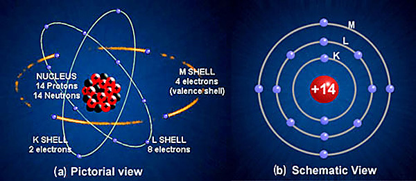
Figure 1.0.2. Two ways of Illustrating The Silicon Atom
Silicon Atom
Figure 1.0.2 Illustrates the structure of an atom of silicon, a very common element widely used in electronics. Figure 1.0.2(a) shows how the basic (simplified) structure of the atom may be imagined, with a nucleus consisting of 14 protons (shown in red) and 14 neutrons (shown in black), surrounded by 14 (blue) electrons orbiting the nucleus in a number of ‘electron shells’. A pictorial diagram like this gives an understandable impression of the atom, a system not unlike a planetary one with orbiting satellites. However in this view it is not easy to show important features of any but the simplest atoms. Different branches of science illustrate atoms in different ways depending on what features are important to the explanation being illustrated. In electronics a simplified ‘Schematic’ diagram like that in Figure 1.0.2(b) is often used. Here the electrically important characteristics of the silicon atom are shown. The 14 electrons in their various shells with the 14 protons of the nucleus, are shown simply as one large ball having a positive charge of +14, balancing the 14 negative charges of the electrons. Because the Neutrons have no electric charge they are ignored.
Figure 1.0.2(b) shows a 2 dimensional view of the electrons orbiting the nucleus in a strict pattern of electron shells. Any particular electron can move around the nucleus in 3 dimensions and can at any time be at any point around the nucleus, rather like a satellite orbiting the earth. However it must orbit at a certain distance from the nucleus. To orbit further out from the nucleus would mean that the electron must gain energy from somewhere, and to orbit closer to the nucleus would mean that the electron would have to lose energy to somewhere.
Electron Shells

Figure 1.0.3
Electron Shells
Each electron shell is a fixed distance from the nucleus, between each shell is a ‘forbidden gap’. For an electron to move to another shell it must gain or lose sufficient energy to move to the next shell in one ‘jump’. When an electron loses energy and jumps to a lower shell (energy level) the energy may be given out as heat or light; it is this loss of energy as light that makes a light emitting diode (LED) glow.
There are up to seven electron shells around an atom and are named using the letters K (for the shell closest to the nucleus) L, M, N, O, P and Q. Some atoms (e.g. hydrogen and helium) have only one shell (the K shell) whereas very complex atoms such as uranium have electrons in all seven shells. The maximum number of electrons each shell can hold is also fixed as shown in Fig. 1.0.3.
The total number of electrons in a particular atom will equal the number of protons and is constant for each element. The distribution of the electrons between shells is also always the same for any particular element. Each shell can hold less electrons than its maximum number, but not more.
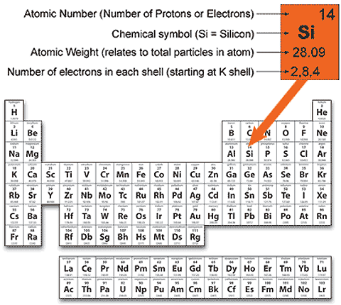
Figure 1.0.4. Silicon described in a Periodic Table
Electrons per Shell
The distribution of protons, neutrons and electrons in each of the elements found in nature is given in a Periodic Table of Elements (Fig.1.0.4). Many different versions of this table can be found in textbooks on physics and science. It is a table setting out the important properties of all known elements, mostly natural, but some man-made elements too. The elements are usually arranged in sequence beginning with hydrogen, which has the smallest atomic weight (atomic weight is a measure of the total mass of all the particles in an atom) and the simplest structure, and ending with a series of elements (some man made) which are very complex and have the largest number of particles in their structure. Each element is illustrated by the information in one box within the table. Of particular interest to electronics engineers are the numbers of electrons in the various electron shells, given at the bottom of each box. Silicon, for example has the maximum number of 2 electrons in its K shell, 8 in its L shell, but only 4 out of a possible 18 electrons in its (outer) M shell. These outer electrons are also called valence electrons and it is these electrons that can be made to migrate from atom to atom when an electric current flows through the silicon. (The inclusion of the number of electrons per shell is often omitted in periodic tables but is useful for electronics purposes).
The Electrical Properties of Materials
Any material can be considered as belonging to one of three groups, depending on its ability to pass an electric current.
1. Conductors pass current readily.
An electric potential applied across a conducting material will cause valence electrons to become detached from their atoms and move (as they are negatively charged) towards the positive potential. As an electron leaves its atom, that atom is of course deficient of negative charge and becomes a positively charged ion. This makes it attractive to another electron which takes the place of the one just attracted away, and so on. Thus a flow of electrons moves, atom by atom towards the positive terminal, being replaced by an excess of electrons at the negative terminal.
The effects of temperature on a conductor.
Heating a conductor causes a vibration within the atomic structure of the material, and this vibration ‘shakes loose’ some of the more easily detached electrons allowing them to migrate randomly from atom to atom. As temperature rises within the conductor, the vibration of the atomic structure increases, and so there are more free electrons being shaken loose from their orbits. This gives rise to more collisions between the randomly moving electrons and the electrons moving under the influence of the electric potential. This makes the flow of electrons towards the positive electrical potential more difficult. Therefore the resistance of a conductor slightly increases as its temperature rises.
In a conductor there are a large number of easily detached electrons within the structure. Some of these electrons are already moving randomly about the structure due to thermal energy (heat) at room temperature, and are called free electrons. Applying an electric potential across the conductor greatly increases the number of free electrons as they move from the negative to positive terminal as previously described. As these free electrons travel through the structure however, they are bound to collide with some of the electrons moving under the influence of heat, as well as being attracted to individual atoms as they jump from one atom´s valence shell to the next. It is these collisions and the pull of individual atomic nuclei, which give the material the electrical property of resistance. The resistance of a material indicates how well or how badly the material conducts (i.e. allows the movement of electrons under the influence of an electric potential or voltage). The higher the value of resistance, the more difficult it is to move the electrons. Materials with higher resistance will therefore need a higher potential (higher voltage) applied to cause a given amount of current, (movement of electrons).
2. Insulators
An insulator has all its electrons tightly bonded to the nucleus and so it takes very large forces of either heat or potential to dislodge them. Insulators do not normally pass current. In some cases, for example at high temperatures or with very high voltages applied, some insulating materials will conduct. In these circumstances the insulating material is said to have ‘Broken down’ and usually the structure of the material is permanently damaged. In some insulators (glass for example) heating the material to a high temperature will vibrate the atoms so violently that enough electrons will be shaken free for conduction to occur. Allowing the glass to cool again stops conduction. In most insulators however, conduction, whether caused by excessive heat or by excessive voltage, will permanently destroy the material. For this reason any material used for electrical insulators, will have a safe working limit quoted by the manufacturer of the insulator,for both voltage and temperature.
3. Semiconductors
Semiconductors fall between groups 1 and 2. They do not normally pass current easily at room temperature, having a resistivity higher than conductors, but lower than insulators. They have properties however which make them very useful for the manufacture of electronic devices such as transistors and diodes.
The difference between the three groups of materials lies in the number of easily detached electrons within the atomic structure. The electrons concerned are more or less loosely held in the outermost electron shells called valence shells and so these electrons are called valence electrons.
In a semiconductor the bond between the valence electrons and their nucleus is much stronger than in a conductor, so far fewer electrons are free to move when a potential is applied. When current does flow, the chances of a collision between the electrons moving due to the electric potential, and randomly moving electrons due to heat, is much less. Additionally the heating of the material frees electrons previously held by their atoms and so these electrons are also free to add to the current flow. Although of course the total current flow is much less than in a conductor, the amount by which current flow increases due to heat is proportionally greater. In use therefore, it is important to keep components made from semiconductor materials, such as transistors, cool. Otherwise an effect called thermal runaway can occur. This is when an increase in temperature causes an increase in current, which in turn causes a further increase in temperature, leading to further increasing current. A process that can escalate until the material passes so much current it is destroyed.
Semiconductor Materials
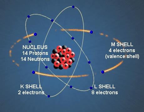
Fig.1.1.1 A Silcon Atom.
Some materials, such as copper, aluminium and brass pass electric currents very easily. As they conduct electricity readily, their ability to resist the flow of current is low. They therefore have very low resistivity and so are classed as conductors.
Other materials such as plastics or glass have extremely high resistivity so do not conduct electricity. These materials are called insulators.
Materials that have a resistivity mid-way between the conductors and insulators do conduct current, but very poorly at normal room temperatures, and so these are called semi-conductors.
How well or poorly any material conducts electricity depends on the atomic structure of the material. For an explanation of the atomic structure of materials as applied to electronics, see our page on The Atomic Structure of Matter.
Silicon and Germanium, as well as a number of other materials and mixtures of materials in the semiconductor group are widely used in the manufacture of transistors and diodes, as well as integrated circuits such as microprocessors.
Semiconductor Doping
To make such semiconductor materials suitable for use in transistors and diodes, the resistivity of the material is modified in a controlled way by first making very pure crystals of the semiconductor material. These crystals contain only atoms of one type (for example silicon) arranged in a regular lattice formation. This very pure material is then ‘doped’ by adding tiny amounts of impurity atoms (about 1 impurity atom in every 10 million).
The idea is that pure semiconductors conduct poorly, because the electrons in their lattice structure are mostly bound very tightly to their atoms, leaving only a few electrons free to move, from atom to atom, through the material, so forming a very weak electric current. By adding impurities with different atomic structures either more or in other cases less, free electrons are added. This controls the ability of the semiconductor to pass current, by effectively changing the resistivity of the material.
Some impurities such as Arsenic and Phosphorus add extra free electrons (negative charge carriers) to the material. This is called N type semiconductor.
Other impurities such as Aluminium and Boron can be added in order to remove free electrons, so that the resulting material has fewer free electrons than before. Each missing electron within the crystal structure is called a "hole". As free electrons are negative charge carriers, these holes in the structure are really positive charge carriers. Material doped in this way is called P type semiconductor. Putting P type and N type materials next to each other in a circuit creates a PN junction, and makes a useful device that is called a diode. When a voltage is applied across a diode a current will flow through the diode in one direction but not the other.
Making a three-part sandwich (PNP or NPN) and carefully controlling the levels of doping in the three layers creates a transistor capable of amplification, as well as many other useful functions.
Semiconductor Materials in Electronic Devices.
Transistors, diodes and integrated circuits can all be classified as semiconductor devices because they are made from semiconductor materials. Early types of transistors and diodes were made from Germanium (Ge), but Silicon (Si) is used today for the vast majority of devices. Germanium is very rarely used in modern transistors however, but does possess some properties that make it useful for devices such as photovoltaic cells to produce electricity in the presence of light. Gallium(Ga) is also used in electronic devices such as light emitting diodes (LEDs), usually as a compound material, i.e. in combination with other materials such as Gallium Arsenide(GaAs) or Gallium Arsenide Phosphide (GaAsP)
Opto Coupled Devices
Opto Devices & Photo transistors
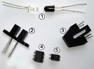
Fig. 5.0.1 Transistor Optocouplers
& Opto Sensors
Optocouplers or opto isolators consisting of a combination of an infrared LED (also IRED or ILED) and an infra red sensitive device such as a photo diode or a photo transistor are widely used to pass information between two parts of a circuit that operate at very different voltage levels. Their main purpose is to provide electrical isolation between two parts of a circuit, increasing safety for users by reducing the risk of electric shocks, and preventing damage to equipment by potential short circuits between high-energy output and low-energy input circuits.
They are also used in a number of sensor applications to sense the presence of physical objects.
Transistor Optocouplers
The devices shown in Fig. 5.0.1 use photo transistors as their sensing elements as they are many times more sensitive than photo diodes and can therefore produce higher values of current at their outputs.
Example 1 in Fig. 5.0.1 illustrates the simplest form of opto coupling consisting of an infrared LED (with a clear plastic case) and an infrared photo transistor with a black plastic case that shields the photo transistor from light in the visible spectrum whilst allowing infrared light to pass through. Notice that the photo transistor has only two connections, collector and emitter, the input to the base being infrared light.
Examples 2 and 3 in Fig 5.0.1 are typical opto coupled devices widely used as position and proximity sensors, these are used as optically activated switches and are described in more detail in Module 5.4.

Fig. 5.0.2 The 4N25 Optocoupler
Example 4 in Fig. 5.0.1 is a 4N25 opto coupler in a 6 pin DIL integrated circuit from Vishay. It uses an output photo transistor with a base connection that is also connected to an external pin for applying an external circuit if required. This allows the opto coupler to have a DC bias applied to prevent the transistor from producing current at very low light levels. Biasing the photo transistor can also enable it to be used with signals such as analogue audio, as described in Module 5.3. In this case the emitter connection can be left unconnected and the base connection used as an output, then the output photo transistor collector/base junction operates as a photo diode, greatly increasing the frequency range of the opto coupler, but at the expense of greatly reducing the available signal amplitude at the output. The 4N25 can also operate as a digital opto coupler with logic 1 and logic 0 inputs. The isolation between input and output on the 4N25 is a minimum of 5.3 kV.
Example 5 in Fig. 5.0.1 is a PC817 4 pin single channel opto isolator chip from Sharp, which uses an integral infra red LED and a photo transistor to produce an output of up 50mA and provides electrical isolation up to 5kV. It is also available in 2, 3 and 4 channel versions.

Fig. 5.0.3 Basic Photo transistor Structure
Photo transistors
Fig. 5.0.3 shows the basic structure of a photo transistor Its operation is similar to the photo diodes described in Diodes Module 2.7. However because the conversion from light to current takes place in a transistor, the tiny current produced by a particular level of photon input to the base can be amplified to produce a collector current 200 times greater or more, depending on the hfe of the transistor, making the photo transistor much more efficient than a photo diode However, because of the large junction area (and therefore much higher junction capacitance) of a photo transistor, its response at high frequencies is poor, and the switching time is much slower, compared to a photo diode Also the relationship between changes in light input and changes in output voltage is not as linear as in photo diodes Consequently photo transistors, though less useful than photo diodes for high frequency data transmission, are widely used in control applications such as opto couplers/isolators, and position sensors.
Photo transistor Operation
In a photo transistor, light, in the form of photons is collected in the base layer, which occupies the major part of the visible window on the top surface of the device, as illustrated in Fig. 5.0.3. The emitter area is therefore reduced in size to maximise light absorption in the base.
The conversion between photons and current takes place largely in the depletion region around the base/collector PN junction where photons absorbed via the anti-reflective layer into the base layer dislodge electrons to create electron/hole pairs in a similar manner to that in photo diodes, but now the free electrons created by this process are the source of base current in the transistor, and are now amplified by an amount equal to the hfe of the transistor.
The N type collector immediately beneath the depletion layer has a higher resistance than the N+ layer next to the collector terminal. Because of this higher resistance close to the PN junction, there is a large voltage gradient in the collector close to the base/collector junction. This provides a higher positive voltage close to the depletion layer to attract and accelerate the negatively charged electrons in the depletion layer towards the collector terminal.
Compared to photo diodes however, photo transistors do have some drawbacks; their response to varying levels of light is not quite so linear, making photo transistors less suitable than photo diodes for accurate light measurement.
Although photo transistors can be used to detect light sources across the visible light spectrum, they are most sensitive to wavelengths in the near infrared range around 800 to 900nm, and are most often used with infrared emitting sources such as infrared emitting LEDs (also called IREDs or ILEDs) as their light source.
Photo transistors are generally not as fast as photo diodes at reacting to abrupt changes in light levels. For example, the time taken for the photo transistor output to change between 10% and 90% in response to a sudden change in light level at the input can be between 30 and 250µs whereas high speed photo diodes can have rise and fall times as low as 20ps (pico seconds) or less. Manufacturers normally quote these figures for rise time (tr) and fall time (tf) under particular conditions of temperature and collector current.
The main reason for the much slower response in photo transistors is due to the much larger area of the base/collector junction, and the fact that the capacitance that exists across this junction is further magnified by the 'Miller Effect', which causes the junction capacitance to be magnified by the current gain (hfe) of the transistor. In practice this means that the more sensitive the transistor (i.e. the larger the base area) and/or the higher the current gain of the transistor, the longer the rise and fall times will be. For these reasons photo transistors are mostly used for switching DC or low frequency AC applications.
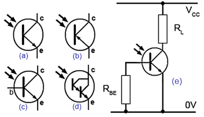
Fig. 5.0.4 Photo transistor Connections
Photo transistor Connections
Photo transistors are available in several forms such as NPN (Fig. 5.0.4a) or PNP (Fig. 5.0.4b). Many photo transistors only have connections for the emitter and collector, as the base input is provided by light; however a base connection is provided on some types (Fig. 5.0.4c).
Darlington photo transistors (Fig. 5.0.4d) are also available; using a Darlington pair transistor configuration gives even greater current gain.
At low or even no light levels, photo transistors can still produce a small amount of current due to random collisions in the depletion layer. Applying base bias as shown in Fig. 5.0.4e can have the effect of preventing this 'Dark Current', so reducing the effect of random noise and giving a better defined on/off level to the output current.
Optocouplers have many uses and are available in many varied types, a few examples are illustrated in Fig. 5.0.5. Use the type numbers to search for data sheets and use them to identify the purpose of each design.
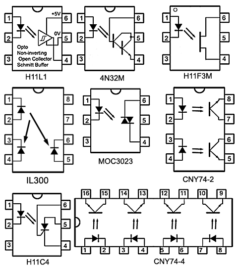
Fig. 5.0.5 Opto coupler Examples
Optocoupler Operation
Optocouplers/OptoIsolators
Optocouplers or opto isolators are used for passing signals between two isolated circuits using different methods, depending mainly on the types of signals being linked. A computer system and its peripheral devices may need a digital signal, such as pulse width modulation signal driving a motor. In this case the optocoupler will be used in Saturation Mode.
A switched mode power supply may need a DC sample voltage of varying value to be fed back from the output to a voltage control system in the input circuit of the power supplywhilst maintaining complete electrical isolation between the input and output circuits. In this case Linear Mode will be used, as the control circuit will need to detect small changes in DC voltage.
To link circuits such as audio amplifiers where signal voltages are rapidly changing, but saturation and distortion need to be avoided, optocouplers can transfer signals using Analogue Mode so that audio can be safely transmitted, for example from an audio input device to a high powered amplifier.

Fig. 5.1.1 Saturation Mode
Saturation Mode
In saturation mode, the optocoupler output transistor is either turned fully 'on' (saturation conditions), or fully 'off' (non-conducting). Optocouplers working in saturation mode are widely used to protect the output pins of micro controllers for example, where they may be used to drive output devices such as motors that may need more current and/or higher voltages than can be supplied directly from the micro controller port.
The micro controller is then effectively only driving an infrared LED, either with signals such as pulse width modulation, stepper motor data or simple on and off signals. The isolation provided by the optocoupler means that the micro controller is also protected from any externally produced high voltages, such as the back emf that may be produced when switching off an inductive load such as a motor. Optocouplers also find uses in modems providing isolation between computers and the external phone lines.

Fig. 5.1.2 Linear Mode
Linear Mode
Optocouplers can be used for voltage feedback in circuits such as switched mode power supplies, where the LED is illuminated by a sample of the output voltage so that any voltage variations cause a variation in the illumination of the optocoupler LED and therefore a variation in the conduction of the optocoupler's output transistor, that can be used to signify an error to the power supply control circuitry, allowing it to compensate for the output variation. A practical example of this feedback and the electrical isolation it provides by using an optocoupler in linear mode can be seen in our Power Supplies Module 3.4 where IC3 (a 4N25) provides a sample of the output voltage to be fed back to an error amplifier controlling the voltage regulator circuit within IC1, providing automatic voltage control, whilst giving complete electrical isolation between the 5V DC output circuit and the higher voltage input circuit.

Fig. 5.1.3 Audio Input in Analogue Mode
Analogue Mode
Like linear mode, the phototransistors used in analogue mode are not allowed to saturate, but a steady DC bias voltage of around half of the supply voltage is modulated by an audio, as shown in Fig. 5.1.3, or some other rapidly varying signal. This produces a varying current in the LED, which in turn produces a varying current in the output component of the optocoupler. This may be a phototransistor or very often a photodiode. The phototransistors used in optocouplers for audio purposes may also make use of a base connection available on some optocouplers to apply a suitable bias to the phototransistor to enable an undistorted audio signal output to be obtained. Specialised audio optocouplers duch as the IL300 shown in Fig. 5.1.4 may use one or more photodiodes in order to provide a more linear response than those using only phototransistors.

Fig. 5.1.4 The IL300 Audio
Optocoupler
In addition to providing a more linear (less distortion) response the second diode is used to provide (isolated) feedback to the input circuit so that the IL300 can automatically compensate for variations in CTR due to changes in temperature and/or aging of the input LED.

Fig. 5.1.5 Audio Input in Analogue Mode
Phototransistor vs. Photodiode Optocouplers
Optocouplers using phototransistor outputs can pass analogue audio signals up to a frequency of a few tens of kHz. Varying the infra red light beam from the LED at these frequencies then causes the amount of current generated at the base of an output phototransistor to vary, with the transistor output following and amplifying the variations at the input.
However optocouplers using phototransistors do not have such as good a linear relationship between the changes in light input and output current as photodiode types, as illustrated in Fig. 5.1.5 therefore some distortion of the signal may occur. Photodiode output devices are preferred for use in most audio (and some digital) applications, even though their output signal amplitudes are much less than is possible with the amplification provided by a phototransistor; the reason for this is the phototransistor's distortion and poor performance at high frequencies.
This is due to the phototransistor having a much-enlarged base area, which whilst increasing the light sensitivity, also greatly increases the capacitance of the base/emitter junction. This increased capacitance is also made much worse because of the 'Miller Effect', which causes the base/emitter capacitance of a transistor to be multiplied by the current gain (hfe) of the transistor. Therefore higher frequencies are progressively reduced in amplitude, because the reactance of the base/emitter capacitance reduces as frequency increases much above the audio range.
Digital signals are also affected by this effect because the square waveforms of digital signals will contain many high frequency harmonics that contribute to the fast rise and fall times of the square wave, so that the rising edges of the signal become rounded and the switching time between 0 and 1 becomes longer.
High speed digital optocouplers, usable at frequencies in the hundreds of kHz and those used for audio operation usually use photodiodes as their sensing element because although some extra amplification must be provided, either externally or within the optocoupler chip itself, this is offset by having fast rise and fall times for digital operation, and a more linear response, producing less distortion when used with analogue audio.
The main function of an optocoupler, whatever type of signal is used, is to provide complete electrical isolation between the input and output circuits. An important advantage of optocouplers, compared with transformers, also often used for isolation purposes, is that optocouplers can be used with either AC or DC signals whereas transformers can only operate with AC.
Using Optocouplers
There are many different applications for optocoupler circuits, so there are many different design requirements, but a basic design for an optocoupler providing isolation for example between two circuits, simply involves the choice of appropriate resistor values for the two resistors R1 and R2 shown in Fig. 5.2.1.
In this example a PC817 optocoupler is shown isolating a circuit using HCT logic via a 7414 Schmitt inverter gate. The Schmitt inverter at the output performs several functions; it ensures that the output conforms to HCT voltage and current specifications, it also provides very fast rise and fall times for the output, and corrects the signal inversion caused by the phototransistor being operated in common emitter mode. Each logic family (e.g. LSTTL or CMOS types) may have different logic voltage levels and different input and output current requirements, and optocouplers can provide a convenient way of interfacing two circuits with different logic levels. What is necessary is to ensure that R1 creates an appropriate current level from the input circuit to correctly drive the LED side of the optocoupler, and that R2 creates appropriate voltage and current levels to supply the output circuit via the inverter.

Fig. 5.2.1 A Simple Optocoupler Interface for HCT
Designing Optocoupler Interfaces
The main purpose of an optocoupler interface is to completely isolate the input circuit from the output circuit, which normally means there will be two completely separate power supplies, one for the input circuit and one for the output. In this simple example the input and output supplies will most likely be the same in voltage and current capabilities, so the interface is just providing isolation without any major shift in voltage or current levels.
In choosing appropriate values for R1, the value for the current limiting resistor is set to produce the correct forward current (IF) through the infrared LED in the optocoupler. R2 is the load resistor for the phototransistor and the values of both resistors will depend on a number of factors.
Current Transfer Ratio
The current in each half of the circuit is linked by the Current Transfer Ratio or CTR, which is simply the ratio of output current to the input current (IC/IF) usually expressed as a percentage. Each optocoupler type will have a range of CTR values set out in the manufacturer's datasheet. The value of CTR also depends on a number of factors, first of all is the type of optocoupler, simple types may have a CTR value of between 20% and 100%, whilst special types, such as those that use a Darlington transistor configuration for their output phototransistor, may have CTR values of several hundred percent. Also the CTR of any particular device may vary considerably from that device's typical value by anything up to +/-30%. Manufacturers will normally quote a range of CTR values for different output phototransistor collector voltages (VC) and different ambient temperatures (TA) The CTR will also vary with the age of the optocoupler, as the efficiency of LEDs decreases with age (over 1000s of operating hours). Because the CTR of an optocoupler can be expected to reduce over time, it is common practice to choose a value for IF somewhat lower than the maximum, so that the intended performance can still be achieved over the intended lifetime of the circuit.
Although this example describes the design of a simple interface linking two HCT logic circuits, the difference between the results achieved here and those needed for any other optocoupler are that similar calculations can be made just using data appropriate to other voltages and currents and other optocouplers.
Calculating the Optocoupler Resistor Values

Fig. 5.2.2 CTR vs. Forward Current for a PC817
The start of the design process is to specify the input and output conditions the optocoupler is to link. Typical optocouplers can handle input and output currents from a few microamps to tens of milliamps. There are many optocouplers on the market and to find the most appropriate for a particular purpose, vendor's catalogues and manufacturers datasheets should be studied.
In this case however, a popular PC817 optocoupler from Sharp will use voltages and currents available from HCT logic. Assuming that a single HCT output is only feeding this optocoupler, a logic 1 voltage of about 4.9V can be presumed.
The output current available from a HCT gate to drive the optocoupler input is limited to 4mA, which is quite low for driving an optocoupler. The PC817 must then be capable of producing the necessary output from this low input current.
The graph in Fig. 5.2.2 shows, the CTR for a PC817 with a forward (input) current IF of 4mA will be around about 80 to 150% allowing ±30% for all the variables mentioned above). Ideally the optocoupler should in this case act as though it is invisible, that is the HCT gate connected to the optocoupler output should see an available current of up to 4mA, just as though it was connected to the output of another HCT gate. Therefore the output current of the PC817 needs also to be ideally about 4mA, with the forward current (IF) driving the input LED at 4mA (assuming a 100% CTR).
Having found an approximate figure for the CTR, which suggests that input and output conditions should be similar, at 4mA, the next task is to calculate the values of R1 and R2.

Using the data in Table 5.2.1 and assuming minimum 4.9V to 5V input at the HCT gate output, it is possible to calculate a suitable resistance value for R1 in Fig. 5.2.3.

Fig. 5.2.3 HCT to HCT Optocoupler
The forward Voltage across the infrared LED with a forward current of only 4mA should be about 1.2V
5V − 1.2V = 3.8V to be developed across R1
Therefore R1 = 3.8V÷4mA = 950Ω
Using the next higher preferred resistor value R1 = 1KΩ
The graph of CTR vs. IF in Fig. 5.2.2 shows that ideally the CTR for the PC817 will be about 115% with a forward current of 4mA, which suggests that the opto output current should be about 4mA x 115% = 4.6mA
To saturate the phototransistor and produce a logic 0 (less than 0.2V) at the output, R2 must develop a voltage of 4.9 to 5V when passing a current of 4.6mA (assuming 115% CTR value).
R2 must therefore be at least 5V÷4.6mA = 1087Ω or R2 = 1.2kΩ (next preferred value).

Fig. 5.2.4a Output with R2 = 1.2KΩ
If a higher value than 1.2KΩ is used, increasing this value by a few kΩ could ensure that the output has the maximum voltage swing, however increasing this value reduces the speed with which the optocoupler can can respond to fast voltage changes, due to the combination of a high resistance load and a high junction capacitance of the phototransistor, which results in a rounding of the output waveform, as can be seen by comparing the waveforms in Fig. 5.2.4 a & b.
Both of the waveforms shown were taken with the same input, a square wave with a frequency of 2kHz, but with two different values for R2, 1.2kΩ in Fig. 5.2.4a and 10kΩ in Fig. 5.2.4b.
The rounding effect on the rise time of the pulses can be clearly seen in Fig. 5.2.4b. Also at higher frequencies amplitude of the output signal reduces markedly. Therefore for best performance the value of R2 should be kept as low as possible, but above 1kΩ.

Fig. 5.2.4b Output with R2 = 10KΩ
The performance of the optocoupler circuit showing the result of using the calculated values is shown in Fig. 5.2.4. Note also the effect of using a 74HCT14 Schmitt inverter at the output; any rounding of the square pulses is eliminated and although the optocoupler output only falls to 0.18V when the phototransistor saturates, the output of the Schmitt gate actually changes between +5V and 0v.
Adding a Schmitt inverter also re-inverts the output waveform, which was an inverted version of the input waveform at the collector of the phototransistor.
There are of course, more useful applications for an optocoupler than simply isolating one logic IC from another. A common problem is driving a load from a computer's output port. Computers are expensive and easily damaged by mistakes made when connecting them to external circuitry. The problem is lessened by ensuring that the external circuit is fully isolated from the computer and an optocoupler such as the PC817 is a cheap and effective (assuming no major user errors) solution.

Fig. 5.2.5 PC817 Motor Drive Circuit
PC817 Motor Drive Circuit
Fig. 5.2.6 illustrates a typical example where it is required to drive a 12V DC motor requiring 40mA of current from a logic circuit (or typical computer port) that can only support a few mA of current at 5V or less.
As the current available from typical computer input/output ports may only be a few µA, as computer port lines are usually designed to drive some type of logic input, the input to this motor drive circuit is via a HCT Schmitt inverter gate, which only requires an input current of 1µA, with the 12V 40mA motor being driven by a 2N3904 transistor. The optocoupler infrared LED is driven at about 4mA via a 1kΩ resistor from IC1 output. As the CTR of the PC817 is around 115% the phototransistor can supply about 9mA as the supply to the phototransistor output is now taken from the 12V motor supply. This is more than the 5mA minimum required to drive the 2N3904 into saturation. It is important that the transistor is fully saturated in order to reduce the power dissipation in the 2N3904 to a minimum, therefore although the transistor current (ICE) is 40mA there will only be about 0.3V across the saturated transistor, so the power dissipation in the transistor will be 0.3V x 40mA = 12mW and the maximum dissipation for the 2N3904 is 1.5W. Although this basic interface only allows for switching the motor on or off, it could easily be adapted by changing IC1 to include a pulse width modulated speed control either from a computer, or hardware generated as described in Oscillators Module 4.6.
This simple interface has one more safety feature; diode D1 connected across the motor will effectively prevent any nasty back EMF spikes generated by the inductive load (the motor) from causing damage to the interface.
Motor Drive Circuit Video
Audio Optocouplers
Using Audio Optocouplers
Fig. 5.3.1 IL300 Optocoupler
In audio systems isolation between inputs and higher voltage/current equipment is usually provided by audio transformers, however it is also possible to use specialised audio optocouplers such as the IL300, which uses an infra red LED to illuminate one photodiode as an output device and a second photodiode to provide feedback, ensuring improved linearity and wider frequency range than phototransistor or photoresistor alternatives. Using feedback from a second photodiode with characteristics closely matched to those of the output photodiode also overcomes a basic problem with optocouplers. Without some sort of feedback, variations in the current transfer ratio will affect the performance of the optocoupler. Variations can occur due to changes in ambient temperature and to ageing of the infrared LED. Optocouplers such as the IL300 from Vishay illustrated in Fig. 5.3.1 can therefore claim both better performance and stability over the lifetime of the circuit. Consequently these specialised devices are considerably more expensive than simple general-purpose optocouplers.
Fig. 5.3.2 4N25 Optocoupler
Using the 4N25 for Audio
However it is also possible to use some of the much cheaper, general purpose phototransistor optocouplers for audio applications, such as the popular 4N25 illustrated in Fig. 5.3.2 also from Vishay, which is normally used for low frequency digital signals (in saturation mode) or DC applications (in linear mode) for limited audio applications.
This is because the 4N25 has a connection for the phototransistor base available, as well as collector and emitter. This allows the three different methods of connection shown in Fig 5.3.3 where the phototransistor can be operated in common emitter mode (a), common collector (emitter follower) mode (b), or used as a photodiode (c).

Fig. 5.3.3 4N25 Connection Choices
When the phototransistor output is taken from the base connection (with the emitter left unconnected) as shown in Fig. 5.3.3(c) the base/collector junction is being used as a photodiode. As the phototransistor now does not function as an amplifier the 'Miller Effect' (where the value of the junction capacitance is multiplied by the current gain of the transistor) does not apply, so the effectively large capacitance of the base/collector junction is greatly reduced, allowing the optocoupler to work at higher speeds, which means in the case of audio applications, a wider bandwidth is available, although this mode of operation greatly reduces the output signal amplitude.
In any of the configurations shown in Fig 5.3.3, the choice of load resistor has a significant effect on the output signal; the higher the value of RL the greater the amplitude of the output signal but the narrower the bandwidth, so the value of RL chosen is a compromise that depends on the purpose of the circuit.
For the 4N25 to provide isolation for audio signals the input to the infrared LED must be appropriately biased with a DC voltage, so that when a modulating AC (audio) signal is applied, the current through the LED can be varied without the optocoupler output reaching either saturation or cut off. This is really an extension of the linear mode of operation, and can be applied using either one of two basic configurations, phototransistor or photodiode.

Fig. 5.3.4 Audio Isolator Using Phototransistor Mode
Method 1. Basic Audio Optocoupler.
The circuit shown in Fig. 5.3.4, adapted from a design in Newnes Electronic Circuits Pocket Book by Ray Marston (ISBN 10:1-4832-9192-8) uses the 4N25 connected as a phototransistor to pass audio signals whilst isolating the input and output circuits.
An LM324 op amp is used here to drive the LED input of the 4N25. R1 and R2 form a potential divider to set pin 3 (the non-inverting input of the op amp) to half of the supply voltage and the audio input signal is superimposed on this DC bias voltage via C1 to modulate the current through the LED.
Because the LM324 is connected in voltage follower mode with the LED forming part of the negative feedback loop, pin 1 exactly follows the voltage variations at pin 3, so varying the current though the LED. With no signal applied the standing current though the LED is about 0.5 to 1mA depending on the value of R3 and the supply voltage used for the input circuit.

Fig. 5.3.5 Audio Bandwidth Using Phototransistor Mode
With separate input and output supplies set at 12V and an AC input signal of 3Vpp, an output signal of around 6Vpp is obtained when RV1 is adjusted to set pin 4 of the 4N25 to about half supply (6V). Depending on supply voltages and the amplitude of signals used, fine adjustment of RV1 also provides a means of achieving minimum distortion.
However, because Fig. 5.3.4 uses a 4N25 in phototransistor mode, the useful bandwidth of the circuit is rather limited, as shown in Fig. 5.3.5 making it useful for speech, but lacking gain at frequencies above 8kHz, a typical effect due to the large base/emitter junction capacitance of the phototransistor.

Fig. 5.3.6 Audio Isolator Using a 4N25 in Photodiode Mode
Method 2 Wide Bandwidth Audio
Fig. 5.3.6 shows an improved circuit with a full audio bandwidth, achieved by using the 4N25 in photodiode mode where only the collector base junction is used, forming a photodiode with much less capacitance than with the full phototransistor. The downside of this method is that the 4N25 output is now reduced to milli-volts rather than volts. For this reason it is necessary to add a buffer amplifier (IC3a) having high input impedance, immediately after the optocoupler.

Fig. 5.3.7 Audio Bandwidth Using Photodiode Mode
No voltage amplification takes place in the buffer stage, but this is followed by a x100 voltage amplifier to produce an output of approximately 7.5Vpp from an original input of 1.5Vpp. The audio bandwidth of the circuit is now increased to cover a useful range from about 400Hz to 18kHz as shown in Fig. 5.3.7; still not hi-fi but quite useful as part of an audio amplifier for many isolation purposes.
In the experimental (breadboard) version of this circuit different supply voltages between +5V and +24V were used for both input and output sections of the circuit without any problems apart from the lower supply voltages requiring signals of reduced amplitude to avoid distortion.
Noise generated around the optocoupler on the breadboard could be a problem but may be reduced or eliminated by careful PCB design, and extra decoupling of the supply lines close to the ICs.

Fig. 5.3.8 4N25 Audio Isolator Tests
Opto Activated Switches
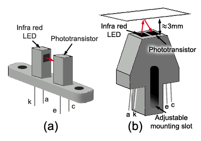
Fig. 5.4.1 Slotted Optical Switch (a)
and Reflective Object Sensor (b
Two typical opto activated switches are illustrated in Fig. 5.4.1. Example (a) is a slotted switch where a beam of infrared light from the LED illuminates a phototransistor, causing it to conduct. When an object is moved into the slot between the LED and phototransistor the light is interrupted and the phototransistor switches off. Opto activated switches are normally operated in saturation mode to provide definite on and off signals.
Another common application for slotted switches is to have a rotating disc, with slots or holes around its rim to spin within the light path of the switch, thereby creating a series of on/off pulses that can be used to indicate (and electronically control) the speed of the spinning disc.
In the reflective object sensor illustrated in Fig. 5.4.1(b) the infrared LED and the phototransistor are mounted side by side in the narrow end of the switch. Here, a beam of infrared light is emitted at an angle by the LED and if some reflective material is placed about 3 to 4mm from the sensor, the light beam from the LED is reflected back onto the phototransistor causing it to conduct and produce an output current. This arrangement is often used as a proximity sensor.
The phototransistor in proximity sensors also operates in 'saturation mode' where the phototransistor is caused to be either off (passing no current) or on (fully saturated, passing its maximum current) by the action of the reflected infrared light.
Slotted Optical Switch Example
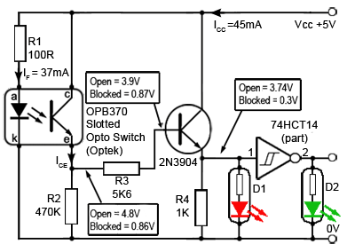
Fig. 5.4.3 Slotted Optical Switch
Circuit
A simple example of a slotted optical switch is shown in Fig 5.4.2, with its schematic diagram in Fig. 5.4.3. When an object such as a ticket, or a small tab that is part of some mechanical system is placed in the sensor slot, the beam of infrared light from the LED to the phototransistor is blocked, turning off the phototransistor. Its emitter terminal, which has been at a high voltage of about 4.8V because the phototransistor has been in saturation and therefore conducting heavily, turns off and the emitter voltage falls to a low value of around 0.8V.
This turns off the 2N3904, which causes its emitter to fall to around 0.3V. This is seen as a logic 0 at pin 1 of IC2 (the input of one of the 6 Schmitt inverters in the IC) and its output at pin 2 changes to logic 1, lighting the green 5V LED. Removing the object from the slotted switch allows the infrared light to reach the base of the phototransistor causing it to conduct and saturate again, which now has a voltage of nearly 5V at its emitter. This switches on the 2N3904 causing a logic 1 (a voltage greater than 2V) to appear at its emitter and the Schmitt inverter input. This turns on the red LED and turns the green LED off.
Fig. 5.4.2 Slotted Opto Switch Sensing a Ticket
The Opto Slotted Switch Interface
The input LED of the slotted OPB370 switch chosen for this demonstration has a maximum current rating of 50mA and the data sheet for the OPB370 shows that at 20mA the forward voltage of the LED will be about 1.3V. To provide a reasonably bright illumination from the LED, it is driven via R1 with IF at about 37mA.
The aim of this design is to drive a single input of a HCT Schmitt inverter gate, which will be responsible for ultimately providing an output that will have very fast rise and fall times and standard HCT voltage and current parameters.
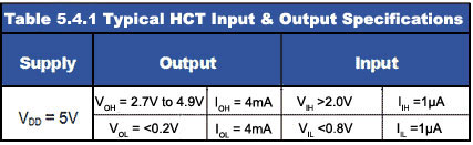
As can be seen in Table 5.4.1, the HCT Schmitt gate will recognise a voltage above 2.0V (VIH) as logic 1 and a low voltage (VIL) below 0.8Vas logic 0. The output current from the 2N3904 must also be sufficient to drive the HCT inverter input, and anything between 1µA and 4mA will be enough.
R1 in the circuit is the current limiting resistor for the input LED and is chosen here to provide a current of about 37mA through the infrared input LED. Note also that the optional 5V LEDs (D1 and D2) used here have an internal current limiting resistor, but a 'normal' LED with appropriate external current limiting resistor could also be used.
Although phototransistor optocouplers produce many times the current produced by photodiode types the output from the phototransistor is still very small and is therefore further amplified by the 2N3904. In addition the 7414 Schmitt inverter provides further conditioning to make the output rise and fall times very fast, and the voltage and current levels ideal for driving HCT digital circuitry. The voltages shown in Fig. 5.4.4 were taken from the working breadboard example shown in Fig. 5.4.2.
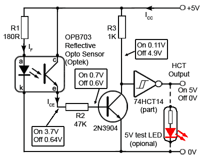
Fig. 5.4.4 Opto Proximity Sensor Circuit
Reflective Object (Proximity) Sensor
These optical sensors work in a similar way to the slotted opto sensor but rely on infra red light reflected from an object (e.g. a sheet of paper in a printer) placed about 2mm to 8mm from the sensor to produce an output. The current produced by the sensor is even smaller than the output currents of the Slotted Switch and therefore also needs to be amplified by a transistor buffer stage to be useful, as shown in Fig. 5.4.4.
A Schmitt Inverter is also added to the output to ensure rapid changes in logic level as a reflective object is detected within the detection range. To avoid sensing errors these sensors work best in low ambient light levels, where the only light sensed by the phototransistor is the reflected light from the infra red LED.
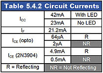
Notice also in both of these switching circuits that only one power source is being used, as electrical isolation between input and output is normally less important. The input to these sensors is light rather than some electrical property. The output is HCT logic, making it suitably conditioned for input to many computer or logic circuit applications. Typical voltages are shown in Fig.5.4.4 and current values in Table 5.4.2
Proximity Detector Circuit Operation
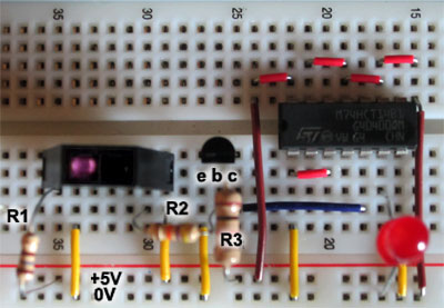
Fig. 5.4.5 Opto Proximity Sensor
Breadboard Layout
R1 is the current limiting resistor for the infrared LED and sets the LED current (IF)at approximately 20mA. The infra red light produced is reflected from an object (plain white printer paper was used in tests) and when in the detection range of about 2mm to 8mm produces a current though R2 of up to about 64µA, dropping to almost zero with no object present (and low ambient light levels).
This current is sufficient to turn on the 2N3904 buffer amplifier transistor and its collector voltage falls from nearly Vcc to almost 0V.
These changes depend on the amount of light reflected into the sensor so may not be fast to change and can be of variable amplitude, however the Schmitt inverter will provide a very fast transition from low to high or high to low at any time the collector voltage of the 2N3904 transistor passes the inverter's threshold values.
Where only a single sensor is required, the use of only 1 out of 6 inverters in the 7414 IC may seem wasteful. The circuit will work without the 7414 inverter, but the switching is much less definite and the output is high without a reflective object being present and low when reflection occurs.
For test purposes, a 5V red LED (with internal current limiting resistor) was used to give a clear indication of the circuit operation. However this can be left out when the circuit is used as an input to another circuit as this will considerably reduce the supply current required, as shown in Table 5.4.2.
The original test circuit is shown in Fig. 5.4.5. Notice that the normally invisible infra red LED shows up as visible (purple) light on a digital camera. Also note that as only the inverter connected between pins 5 and 6 of the IC are being used, the five other unused inputs on the 7414 IC are all connected to 0V to prevent excessive noise being injected into the circuit.
Proximity Detector in Operation
Optocoupler Quiz
Try this quiz based on optocouplers. Hopefully it'll be easy. Submit your answers but don't be disappointed if you get answers wrong. All the information you need is on this website. Find the right answer and learn about transistors as you go.
1.
Amplifier Circuits
Introduction to Impedance and Bandwidth Control
Modified Response Curves
Previous modules have concentrated on producing a flat frequency response over the required audio frequency range. It is sometimes necessary however, to modify the flat response of an audio amplifier by making particular stages of the amplifier frequency dependent. This can be achieved by modifying either the response of one or more of the amplifier stages, or the response of a negative feedback path.
Fig. 4.0.1 shows (shaded green) stages where such modification will take place, the remaining stages having a flat response curve.

Fig. 4.0.1 Controlled Stages of an Audio Amplifier
Input Selection
The input select, or input compensation stage is used to match the input impedance of the amplifier to particular input device types, each of which may have different output impedances, signal levels and frequency ranges. The output of the select stage should therefore give fully compensated signal characteristics and a standard audio signal for any connected input device. It is possible however for a user to connect an input device that does not conform to the manufacturer's recommended specifications, especially as these may differ from one manufacturer to another. The most noticeable result is then, that a change in signal level may be heard when switching between different input devices.
Tone Control
Tone control is used to boost or reduce the high or low frequencies of the audio signal to suit the user's requirements and/or the acoustics of listening environment. Placing this stage immediately before the power amplifier minimises any internally generated noise, which may occur if, for example a treble cut (HF reduction) circuit was followed by a number of full bandwidth amplifiers.
Modifying Input and Output Impedance.
The importance of an amplifier’s input and output impedance is discussed in AC Theory Module 7, and using NFB to control impedance is described in Amplifiers Module 3.2.
This module therefore describes some typical circuits used to control the values of input and output impedance and frequency characteristics of amplifier circuits.

Amplifier Controls


Fig. 4.2.1 Simple Tone Control
Tone Control
Tone Control, shown in its most basic form in Fig. 4.2.1 provides a simple means of regulating the amount of higher frequencies present in the output signal fed to the loudspeakers. a simple method of achieving this is to place a variable CR network between the voltage amplifier and the power amplifier stages, The value of C1 is chosen to pass the higher audio frequencies, this has the effect of progressively reducing the higher frequencies as the variable resistor slider is adjusted towards the bottom end of the tone control, The minimum level of attenuation of the higher (treble) frequencies is limited by R1, which prevents C1 being connected directly to ground. As the circuit only reduces the high frequency content of the signal it could be called a simple Treble Cut control. The use of these simple circuits is normally restricted to guitar applications or inexpensive radios.
In hi-fi amplifiers, tone control refers to the boosting or reduction of particular audio frequencies. This may be done to suit the preferences of the listener, not everyone perceives sound in exactly the same way, for example the frequency response of the human ear changes with age. The room or hall in which the sound is reproduced will also affect the nature of the sound. many techniques are used to alter the sound, and in particular the frequency response of the amplifiers producing the sound. These range from simple RC filters, through passive and active frequency control networks to complex digital signal processing.
The Baxandall Tone Control Circuit

Fig. 4.2.2 Baxandall Tone Control Circuit
The circuit discussed here is an example of the Baxandall tone control circuit, illustrated in Fig. 4.2.2, which is an analogue circuit providing independent control of bass and treble frequencies; both bass and treble can be boosted or cut and with both controls at their mid positions, provides a relatively flat frequency response, as illustrated by the blue ‘Level response’ graph line in Fig. 4.2.5. The original design, proposed by P. J. Baxandall in 1952, used a valve (tube) amplifier and feedback as part of the circuit to reduce the considerable attenuation (about −20dB) introduced by the passive network, and to provide true bass and treble boost. There are still many variants of the circuit in use, both as active circuits (with amplification as originally proposed), and as passive networks without an incorporated amplifier. In passive variants of the Baxandall circuit, extra stages of amplification may be used to make up for the approximately −20bB attenuation caused by the circuit.
Read the original 1952 paper "Negative-Feedback Tone Control" by P. J. Baxandall B.Sc.(Eng.) published in "Wireless World" (Now Electronics World)
How the Baxandall Circuit Works.
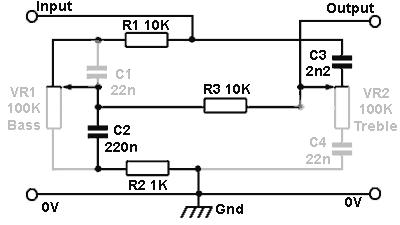
Fig. 4.2.3 Maximum Bass & Treble Boost
With bass and treble controls set to maximum boost (both wipers at the top of resistors VR1 and VR2), and the inactive components greyed out, the circuit will look like Fig. 4.2.3. Both bass and treble potentiometers that may have either linear or logarithmic tracks depending on the circuit design, are much higher values than other components in the circuit, and so with the VR1 and VR2 wipers set to maximum resistance both potentiometers can be considered to be open circuit. Nor does C4 contribute to the operation of the circuit because of the high resistance of VR2, and C1 is effectively shorted out by the wiper of VR1 being at the top end of its resistance track.
The full bandwidth of signal frequencies is applied to the input from an amplifier having low output impedance, and the higher frequency components of the signal are fed directly to the output of the tone control circuit via the 2.2nF capacitor C3, which has a reactance of about 3.6KΩ at 20kHz but over 3.6MΩ at 20Hz, so blocks the lower frequencies.
The full band of frequencies also appear at the junction of R1 and C2, which together form a low pass filter with a corner frequency of around 70 to 75 Hz and so frequencies appreciably higher than this (the mid and high frequencies) are conducted to ground via R2.
Having R2 in series with C2 prevents the attenuation of the mid band frequencies exceeding about -20dB. The lower frequencies are fed to the output via R3. Because R3 has quite a large value (to effectively isolate the effects of the two variable controls from each other, the input impedance (Zin) of the circuit following the tone control must be very high to avoid excessive signal loss due to the potential divider effect of R3 and the Zin of the following stage.
Bass and Treble Cut.
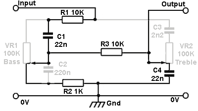
Fig. 4.2.4 The Circuit with VR1 and VR2 at Minimum
With the bass and treble controls both set to maximum cut (Fig. 4.2.4), the full bandwidth signal passes through R1 but with the slider of VR1 at the bottom end of its resistance track, C1/R2 now form a high pass filter having a corner frequency of around 7 to 7.5kHz so only frequencies appreciably higher than this are allowed to pass un-attenuated. The mid and higher frequencies are therefore fed to R3 and C4, which now form a low pass filter to progressively attenuate frequencies above about 70 Hz, the mid-band frequencies (about 600Hz) are reduced by approximately −20dB, and at 20kHz by as much as −43dB, as can be seen from the response curve in Fig 4.2.5.
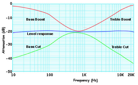
Fig. 4.2.5 The Baxandall Modified Response Curve
Notice that although the circuit provides what is called bass boost and treble boost, with the passive version of the Baxandall circuit (with no amplification), all frequencies are in fact reduced.
The attenuation of the circuit at mid-band is typically around −20dB and with full ‘boost’ applied at either the low or high end of the bandwidth, attenuation at these frequencies would be around −1 to −3dB.
Active Baxandall Circuit
To overcome the substantial losses in the passive version of this circuit, which give a level response (with both controls at mid way setting) but at -20dB below the input voltage, it is common to incorporate an amplifier in the designs. Nowadays an op-amp would be a reasonable choice, with the Baxandall network forming a negative feedback loop to give the required gain figures over the necessary bandwidth. Various designs are possible with different values for resistors R1 to R4 and C1 to C4 in the network, depending to some extent on the output impedance of the previous, and input impedance of the following circuits.
With active circuits such as that shown in Fig. 4.2.6 the aim is to have the level response at 0dB so there is no gain and no loss due to the tone control circuit. The maximum amount of boost possible should not be sufficient to overload any stage following the tone control if distortion is to be avoided. The design of such control circuits is usually therefore, an integral part of the overall design of an amplifier system.

Fig. 4.2.6 An active tone control using a Baxandall network and op-amp with NFB.
Tone Control ICs

Fig. 4.2.7 The LM1036 Audio Control IC
In modern amplifiers the tendency is to use integrated circuit controls that may be operated by either digital or analogue circuitry. A simple solution for bass, treble, balance and volume control in analogue stereo amplifiers is offered by such chips as the LM1036 from National Instruments.
The block diagram and an application circuit is shown in Fig. 4.2.7. Each of the four controls is adjusted by applying a variable voltage of between 5.4V (which is supplied by pin 17 of the IC), and 0V. Half the voltage applied to the control pins 4, 9, 12 and 14 gives a level frequency response, central balance between left and right channels, and half volume.
The LM1036 also has provision for a loudness compensation switch. When ‘on’ this changes the action of the controls to boost the bass and treble frequencies when the volume is at a low setting. The purpose of this is to compensate for the fall off in the function of human hearing at high and low frequencies with quiet sounds.
Amplifiers & Impedance
The input and output impedances of an amplifier are very important parameters that affect the overall gain in multi-stage amplifiers. AC Theory Module 7.2 describes how correct matching reduces signal loss between the output of one amplifier and the input of the next in multi stage amplifiers. This section looks at practical methods of obtaining suitable input and output impedances where amplifiers interface with typical input and output devices such as microphones and loudspeakers.
Audio input sources, such as microphones, pick-ups, radio tuners etc. can have impedances ranging from a few hundred ohms to several thousand ohms. Where audio amplifier inputs may have to cater for a number of different input sources, switch selectable inputs to compensate for specific input devices, as described in Amplifiers Module 4.1.
The final (output) stage in a multi-stage amplifier has to drive a ‘transducer’, which will convert the electrical signal energy produced by the amplifier into some other useful form. For example the electrical waves produced by an audio amplifier will be converted into sound (air pressure) waves by a loudspeaker. A radio frequency (RF) amplifier in a transmitter may be used to drive an antenna (aerial), or a DC amplifier may be driving an electric motor or a relay. Any or all of these transducers may have quite low impedances and require considerable amounts of signal current or power, rather than large signal voltages to operate them. Therefore the output stage of an amplifier may need to have a low output impedance, much lower than would be possible using the common emitter voltage amplifiers described in Amplifiers Module 4.1 to 4.3.
This section describes some types of current and voltage amplifier circuits commonly used to modify input and output impedances. Power output stages are described in Amplifiers Module 5 .
FET Input Stage

Fig. 4.3.2 High Impedance JFET Input Stage
Where very high impedance and low noise is required in an amplifier input, it is common to use a field effect transistor (FET) in an amplifier's input stage. Very high input impedance is obtainable with JFETs as its gate is voltage, rather than current operated. Therefore the JFET takes hardly any current from the device connected to the amplifier input. Even higher input impedances are available where MOSFETs with insulated gate construction (IGFETs) are used. Although FETs generally have less voltage gain and less bandwidth than BJT transistors they also create much less internally generated noise, which makes them ideally suited for use in the early stages of an amplifier, where good signal to noise ratio is important.
Operation
Because the input resistance of the JFET is extremely high, the input impedance of the circuit is approximately the value of R1, and as practically no current is flowing into the input, there is no potential across R1, therefore the gate of Tr1 is effectively at zero volts. To operate correctly, the gate of the N channel JFET must be more negative than the source, this is achieved by making the source of Tr1 positive. The signal applied to the gate will then vary the gate voltage and so vary the drain current through the JFET. The biasing of the JFET is set by R2 and R3. As JFET gain is not particularly high, extra gain is provided by the PNP transistor Tr2. The overall gain of the two-stage amplifier is set at approximately 11 by the negative feedback provided by R4 and R5.
Decoupling

Fig. 4.3.3 Supply Decoupling
(From Fig 4.3.2)
In Fig 4.3.2, R3 is decoupled by C2 so that the bottom end of R4 is effectively at ground potential as far as AC is concerned, the value of C2 is not particularly large in this circuit, as the larger the value of electrolytic capacitor the more noise it will produce, and the aim of the circuit is to keep internally generated noise to a minimum. C1 and C4 coupling capacitors, (also relatively small values) provide isolation from any DC voltages present on any connected circuits. Using a very high value for R1 produces a high input impedance but the higher the value, the more prone the circuit will be to instability and oscillation. To prevent this possibility, effective decoupling from other circuits and the supply is necessary, decoupling here is provided by R6 and C3 as shown in Fig. 4.3.3.
The Emitter Follower

Fig. 4.3.4 Emitter Follower
Common emitter amplifiers generally have a medium to high output impedance, the value depending mainly on the value of load resistor in the final stage of amplification. Many typical transducers, such as loudspeakers, relays, motors etc. are inductive devices having a low impedance of only a few ohms.
Connecting such devices to the output of a voltage amplifier with a load resistance of several thousand ohms will result in poor impedance matching with practically the whole of the output being developed across the load resistor instead of across the load. One answer to this problem is to reduce the output impedance by using an emitter follower, which is a single transistor connected in common collector mode.
Common Collector Mode
This configuration uses the collector lead as the common connection for input and output. In the circuit (Fig. 4.3.4) the input to the transistor is connected between base and ground, and the output is connected across the load resistor between emitter and ground. Remember that with the collector connected directly to the supply, the collector is at ground potential as far as AC is concerned, because of the presence of large decoupling capacitors connected between supply and ground.
The common collector amplifier is called an emitter follower because the output, taken from the emitter is in phase with and ‘follows’ the input voltage at the base. In fact the base and emitter voltages are almost identical so the emitter follower has a voltage gain of 1 (in practice, slightly less) because of the 100% negative feedback created by the emitter load resistor not being decoupled, as would be the normal case in a common emitter amplifier. This causes the full amplitude of the output signal to be fed back to the base, giving a closed loop gain β of 1.
The emitter follower is therefore of no use as a voltage amplifier. It does however, have other very useful properties. Its current gain is large, and approximately equals the current gain (hfe) of the transistor. The input impedance of the circuit is high, 100KΩ or more being typical, although this will depend to some extent on the value of the base bias resistor R1 in Fig. 4.3.4, which is in parallel with the input resistance of the transistor, but this shunting effect can be reduced by ‘Bootstrapping’. The output impedance of the circuit is very low, typically in the region of 50Ω. Because of its use in matching relatively high output impedance voltage amplifiers to low impedance loads, the emitter follower may also be called a ‘Buffer Amplifier’.
The Emitter Follower as a Voltage Regulator

Fig. 4.3.5 Emitter Follower Voltage Regulator
Another use for the emitter follower is as a voltage regulator, and is useful in power supplies where a small voltage can be used to regulate a large current., as shown in Fig. 4.3.5. This circuit ensures that the regulated 5 volt supply remains at the correct voltage even if the 12 volt supply changes. An accurate five volts is also maintained for a range of currents drawn by the circuit being supplied. Regulation can be achieved just using a resistor and Zener diode combination but much higher currents can be handled when an emitter follower is used.
Notice in Fig.4.3.5 that the Zener diode has a voltage rating of 5V6 (meaning 5.6volts), this will maintain the base of the transistor at that voltage, and the emitter of the transistor at 0.6V below the base voltage, will be maintained at 5 volts. A small current maintaining the base voltage at 5.6V is therefore able to accurately control a much larger current flowing through the collector and emitter.
The emitter follower circuit is also the basis of many push-pull class B and class AB power output amplifier stages described in Amplifiers Module 5
The Emitter Follower Converted to a Darlington Pair

Fig. 4.3.6 The Darlington Pair
The effect of a high input impedance is to reduce the input current to the amplifier. If the input current for a given input voltage is reduced by whatever method, the effect is to increase the input impedance. The emitter follower has a high input impedance, but this may be reduced to an unacceptable level by the presence of the base bias resistor.
However another circuit, the compound or Darlington pair shown in Fig. 4.3.6 can greatly increase input impedance. By using one emitter follower (Tr1) to drive another (Tr2) the overall current gain becomes the product of the individual gains, hfe1 x hfe2 and can be typically 1000 or more. This greatly reduces the signal current required by the base of Tr1 and thereby dramatically increases the input impedance.
The Darlington Pair using Common Emitter Amplifiers

Fig. 4.3.7 Common Emitter Arrangement
The Darlington pair can also be used in common emitter mode, as shown in Fig. 4.3.7. Darlington transistors are also available as combined packages in both PNP and NPN types, complete with back emf protection diodes typically required when the Darlington configuration is used as a high current gain output device for switching high current inductive loads.

Fig. 4.3.8 The Darlington Integrated Circuit ULN2803
Darlington amplifiers are also available in integrated circuit form, such as the ULN2803, which contains eight high current, Darlington amplifiers with open collector outputs, for interfacing between TTL (5V) logic circuits and high current/high voltage (up to 500mA and 50V) devices. When pin 10 is connected to +V each output is diode protected for driving inductive loads against back e.m.f.
Bootstrapping
Bootstrapping (Using positive feedback to feed part of the output back to the input, but without causing oscillation) is a method of apparently increasing the value of a fixed resistor as it appears to A.C. signals, and thereby increasing input impedance. A basic bootstrap amplifier is shown in Fig. 4.3.8 where capacitor CB is the ‘Bootstrap Capacitor’, which provides A.C. feedback to a resistor in series with the base. The value of CB will be large, about 10 x the lowest frequency handled x the value of the series resistor (10ƒminR3).

Fig. 4.3.8 Bootstrapping applied to an Emitter Follower
Although positive feedback is being used, which would normally cause an amplifier to oscillate, the voltage gain of the emitter follower is less than 1, which prevents oscillation.
In Fig. 4.3.8 the base of the emitter follower is biased from a potential divider via R3. By feeding the output waveform back to the left hand side of R3 the voltage at this end of R3 is made to rise and fall in phase with the input signal at the base end of R3.
Because the output waveform of the emitter follower is a slightly less amplitude than the base waveform (due to the less than 1 gain of the transistor) there will be a very small signal current waveform across R3. Such a small current waveform suggests a very small current is flowing; therefore the resistance of R3 must be very high, much higher than in fact it is. The input impedance of the amplifier has therefore been increased.
The effective A.C. value of R3 is increased by R3 ÷ (1 −Ao) where Ao is the open loop gain of the amplifier.
For example a 47KΩ resistor with bootstrapping would appear to be:

So if AO = 0.98 the apparent value of R3 would be 47 x 103 ÷ (1- 0.98) = 2,35MΩ
The main drawback of this method of increasing input impedance compared with other methods is that the use of positive feedback is likely to increase noise and distortion.
Introduction to Power Amplifiers

Power Amplifiers
Amplifier circuits form the basis of most electronic systems, many of which need to produce high power to drive some output device. Audio amplifier output power may be anything from less than 1 Watt to several hundred Watts. Radio frequency amplifiers used in transmitters can be required to produce thousands of kilowatts of output power, and DC amplifiers used in electronic control systems may also need high power outputs to drive motors or actuators of many different types. This module describes some commonly encountered classes of power output circuits and techniques used to improve performance.
The voltage amplifiers described in Amplifiers Module 1, Module 2, Module 3, & Module 4 can increase the amplitude of a signal many times but may not, on their own, be able to drive an output device such as a loudspeaker or motor.
For example a voltage amplifier may have a gain of 100 and be able to amplify a 150mV signal to an amplitude of 15V and it is quite possible that the amplifier can feed that 15V signal into a load of say 10KΩ, but if the load is changed to a value of 10Ω, the voltage amplifier would not be able to provide the extra current needed to maintain an output voltage of 15V across 10Ω.
Likewise, a current amplifier may have a gain of 100 and be able to amplify a 10µA signal to 1mA at a very low output voltage, but be unable to supply a 1mA signal at say 10V.
In either case the voltage or current amplifier does not have sufficient POWER (volts V x current I). Voltage and current amplifiers can make use of small transistors and do not draw large amounts of power from the power supply in order to amplify signals by often, very large amounts. However the small transistors they use have very tiny junction areas and so cannot handle the power needed to drive some output devices without overheating.
Power Transistors and Heat Sinks
Power Transistors
There is not a clear cut difference between ‘ordinary’ transistors used in voltage amplifiers and power transistors, but generally Power transistors can be categorised as those than can handle more than 1 Ampere of collector (or Drain in the case of FETs) current.
Because power transistors, such as those shown in Fig. 5.1.1 handle larger currents and higher voltages, they have a different construction to small signal devices. They must have low output resistances so that they can deliver large currents to the load, and good junction insulation to withstand high voltages. They must also be able to dissipate heat very quickly so they do not overheat. As most heat is generated at the collector/base junction, the area of this junction is made as large as possible.
Power and Temperature
The maximum power rating of a transistor is largely governed by the temperature of the collector/base junction as can be seen from the power de-rating graph in Fig. 5.1.2. If too much power is dissipated, this junction gets too hot and the transistor will be destroyed, a typical maximum temperature is between 100°C and 150°C, although some devices can withstand higher maximum junction temperatures. The maximum power output available from a power transistor is closely linked to temperature, and above 25°C falls in a linear manner to zero power output as the maximum permissible temperature is reached.
Power De-rating

Fig 5.1.2 Power de-rating Graph for the TIP31
For example, a transistor such as the TIP31 having a quoted maximum power output PTOT of 40W can only handle 40W of power IF the case temperature (slightly less than the junction temperature) is kept below 25°C. The performance of a power transistor is closely dependant on its ability to dissipate the heat generated at the collector base junction.
Minimising the problem of heat is approached in two main ways:
- 1. By operating the transistor in the most efficient way possible, that is by choosing a class of biasing that gives high efficiency and is least wasteful of power.
- 2. By ensuring that the heat produced by the transistor can be removed and effectively transferred to the surrounding air as quickly as possible.
Method 2 above, highlights the importance of the relationship between a power transistor and its heat sink, a device attached to the transistor for the purpose of removing heat. The physical construction of power transistors is therefore designed to maximise the transfer of heat to the heat sink. In addition to the usual collector lead-out wire, the collector of a power transistor, which has a much larger area than that of a small signal transistor, is normally in direct contact with the metal case of the transistor, or a metal mounting pad, which may then be bolted or clipped directly on to a heat-sink. Typical metal cased and metal body power transistors are shown in Fig. 5.1.1
Because power amplifiers generate substantial amounts of heat, which is wasted power, they are made to be as efficient as possible. With voltage amplifiers, low distortion is of greater importance than efficiency, but with power amplifiers, although distortion cannot be ignored, efficiency is vital.
Heat Sinks

Fig 5.1.3 Heat-sinks
A heat-sink is designed to remove heat from a transistor and dissipate it into the surrounding air as efficiently as possible. Heat-sinks take many different forms, such as finned aluminium or copper sheets or blocks, often painted or anodised matt black to help dissipate heat more quickly. A selection of heat-sinks is illustrated in Fig. 5.1.3.
Good physical contact between the transistor and heat-sink is essential, and a heat transmitting grease (heat-sink compound) is smeared on the contact area before clamping the transistor to the heat-sink.
Where it is necessary to maintain electrical insulation between transistor and heat-sink a mica layer is used between the heat-sink and transistor. Mica has excellent insulation and very good heat conducting properties.
Choosing the Right Heat-sink

Fig 5.1.4 Fitting a TO220 Heat-sink
Many heat-sinks are available to fit specific transistor package types, (‘package’ refers to the shape and dimensions of the transistor). Fig 5.1.4 shows the various stages in fitting a typical clip on heat-sink.
(a) shows a tube of heat-sink compound.
(b) shows a TO220 clip on heat-sink.
(c) shows a TIP31 transistor, which has a TO220 package type, ready for mounting.
(d) shows the metal body of the transistor smeared with heat-sink compound. This is essential to create efficient heat transfer between the transistor and heat-sink.
(e) shows the transistor fitted to the heat-sink.
(f) shows an alternative method of mounting, used when the metal body of the transistor, (which is usually also the collector terminal), must be insulated from the heat-sink. This example uses a TO220 shaped mica washer, and the transistor is clamped to the heat-sink with a bolt fitted through the small insulating bush.
Typical Rth Calculation for:
- A TIP31 transistor (TO220 package) required to dissipate 5 Watts.
- Maximum Junction Temperature = 150°C
- Ambient (air) temperature = 25°C.
- Thermal resistance between junction and case calculated from power de-rating graph Fig. 5.1.2.
- Rth j-c = (150°C − 25°C) / 40W = 3.125°C/W.
- Max. case temperature when dissipating 5W = 150 − (5 x 3.125) = 134°C (approx).
- Thermal resistance Rth c-hs between case and heat-sink (allowing for mica washer) = 2°C/W.
- Max. heat-sink temperature = 134 - (5 x 2) = 124°C.
- To reach ambient air temperature = 25°C Thermal resistance of heat-sink must be better than (124 − 25) / 5 = 19.8°C/W
- A better choice, to avoid operating the transistor at its maximum permitted temperature, would be to choose a heat-sink with a thermal resistance of about 10 to 15°C/W.
Calculating the Required Thermal Resistance Rth for a Heat-sink
The heat-sink chosen must be able to dissipate heat from the transistor to the surrounding air, quickly enough to prevent the junction temperature of the transistor exceeding its maximum permitted value (usually quoted on the transistor’s data sheet), typically 100 to 150°C.
Each heat-sink has a parameter called its Thermal Resistance (Rth) measured in °C/Watt and the lower the value of Rth the faster heat is dissipated. Other factors affecting heat dissipation include the power (in Watts) being dissipated by the transistor, the efficiency of heat transfer between the internal transistor junction and the transistor case, and the case to the heat-sink.
The difference between the temperature of the heat-sink and the air temperature surrounding the heat-sink (the ambient temperature) must also be taken into account. The main criteria is that the heat-sink should be efficient enough, too efficient is not a problem.
Therefore any heat-sink with a thermal resistance lower or equal to the calculated value should be OK, but to avoid continually running the transistor at, or close to the maximum permitted temperature, which is almost guaranteed to shorten the life of the transistor, it is advisable to use a heat-sink with a lower thermal resistance where possible.
The power de-rating graph for a TIP31 transistor shown in Fig. 5.1.2 illustrates the relationship between the power dissipated by the transistor and the case temperature. When the transistor is dissipating 5W, it can be estimated from the graph that the maximum safe case temperature, for a junction temperature of 150°C would be about 134 to 135°C, confirming the above calculation of max. case temperature.
The TIP31 transistor has a maximum power dissipation PTOT of 40W but it can be seen from the graph in Fig. 5.1.2 that this is only attainable if the case temperature of the transistor can be held at 25°C. The case temperature can only be allowed to rise to 150°C (the same as the maximum junction temperature) if the power dissipation is zero.
Parallel Transistors for High Power Applications

Fig 5.1.5 Power Transistors Connected in Parallel
With high power applications it may be impossible to find a suitable heat-sink for a particular transistor, then one solution would be to use a different power transistor, or different case (package) type if available. Another alternative is to use two or more transistors connected in parallel, sharing the total power between them. This can be a cheaper option than a single very expensive heat-sink.
Thermal Runaway
In many modern circuits power MOSFETs are preferred to BJTs because of the BJTs problem of thermal runaway. This is a process where current flow rises as a natural effect in semiconductors as the temperature of the device increases. This rise in temperature then leads to a further increase in current flow and a subsequent further rise in temperature, until the rise in temperature and current, spirals out of control and the device is destroyed.
When several poorly matched transistors are connected in parallel, the transistor initially passing the most current will get hotter, whilst the others, passing less current get cooler. Therefore the hotter transistor can be in danger of thermal runaway, however BJTs, carefully matched may still be preferable to MOSFETs for some high voltage applications.
Class AB Power Amplifiers
Class AB Power Amplifiers
The class AB push-pull output circuit is slightly less efficient than class B because it uses a small quiescent current flowing, to bias the transistors just above cut off as shown in Fig. 5.5.1, but the crossover distortion created by the non-linear section of the transistor’s input characteristic curve, near to cut off in class B is overcome. In class AB each of the push-pull transistors is conducting for slightly more than the half cycle of conduction in class B, but much less than the full cycle of conduction of class A.
As each cycle of the waveform crosses zero volts, both transistors are conducting momentarily and the bend in the characteristic of each one cancels out.
Another advantage of class AB is that, using a complementary matched pair of transistors in emitter follower mode, also gives cheaper construction. No phase splitter circuit is needed, as the opposite polarity of the NPN and PNP pair means that each transistor will conduct on opposite half cycles of the waveform. The low output impedance provided by the emitter follower connection also eliminates the need for an impedance matching output transformer.
Matching of current gain and temperature characteristics of complementary (NPN/PNP) transistors however, is more difficult than with just the single transistor type as used in class B operation. Also with no emitter resistors, due to the use of emitter follower mode, temperature stability is more difficult to maintain. Class AB therefore, can have a greater tendency towards thermal runaway.

Fig 5.5.2 Applying Class AB Bias
Fig 5.5.2 illustrates the method of applying the class AB bias to a complementary pair of transistors. The two resistors R1 and R2 apply voltages to the output transistor bases so that Trl (NPN) base is about 0.6V more positive than its emitter, and Tr2 (PNP) base is about 0.6V more negative than its emitter, which is at half of VCC.
To overcome crossover distortion, the bias on the base of each transistor needs to be accurately set so that the transistors will begin to conduct as soon as their respective half cycle begins, it is therefore common for R2 to be made adjustable.
Class AB Complementary Push Pull Output Stage
The output circuit shown in Fig 5.5.3 includes many of the features and techniques described throughout Amplifier Modules 1 to 5. It shows a class AB output stage (Tr2 and Tr3) and a class A audio driver (voltage amplifier) Trl. The circuit features both AC negative feedback to reduce distortion and noise, and widen bandwidth, as well as DC negative feedback to stabilise the DC biasing. There is also some positive feedback, ‘Bootstrapping’ applied to increase input impedance and improve efficiency. Other essential features include the use of diodes to provide thermal stability, and some bias adjustments to give minimum distortion.

Fig 5.5.3 Class AB Output Stage
Operation
Tr1 driver transistor is a class A voltage amplifier fed with a variable amplitude audio signal from the input via the volume control VR1. Bias for Tr1 is provided via the potential divider R2, Vr2 & R3 from the junction of Tr2 & Tr3 emitters, which will be at half of the supply voltage.
DC Bias Stabilisation
Biasing for Tr2 and Tr3 is provided by the current flowing through the loudspeaker (which is also the output load for the amplifier), R5 and VR3. This provides an appropriate base current on Tr2 and Tr3 to make the emitters of Tr2 and Tr3 (the mid-point), half of the supply voltage. Because the base bias for Tr1 (via R2, VR2 and R3) is taken from the emitters of Tr2 and Tr3, if the voltage at the mid-point increases, the bias on Tr1 base will also increase, causing Tr1 to conduct more heavily. The collector voltage on Tr1 would therefore fall, also causing the voltages on the bases of Tr2 and Tr3 to fall. As Tr2 is NPN and Tr3 is PNP this would tend to turn Tr2 off and Tr3 on, reducing the voltage at the mid-point until it returns to its correct value of half supply.
If the voltage at the mid-point falls too far, this will result in a lowering of the bias voltage on Tr1, turning it off and increasing its collector voltage, and also the base voltages of Tr2 and Tr3. This action will increase the conduction in (NPN transistor) Tr2 and decrease conduction in (PNP transistor) Tr3, raising the mid-point to its correct voltage once more.
Temperature Compensation
Dl & D2 are two silicon diodes having a similar junction potential as Tr2 and Tr3. They are connected across the output transistors base/emitter junctions to improve thermal stability. As Tr2 and Tr3 warm up, their base/emitter junction potentials will naturally fall. This would lead to over biasing and more current flow in the transistors, leading eventually to thermal runaway. D1 & D2 are usually mounted on the same heat-sinks as the output transistors. Therefore as Tr2 and Tr3 heat up, so will D1 and D2.
The junction potential of the diodes also falls, and they begin to conduct. Because the voltage between the two output transistor bases is set by VR1 to 1.2V under cold conditions, Dl and D2 are initially just cut off. However if these diode junction potentials fall due to heating, they will begin to conduct and reduce to voltage between Tr1 and Tr2 bases. This will therefore reduce the bias on the output transistors and so maintain correct class AB bias conditions.
Mid-Point Adjustment
It is important that the mid-point voltage is kept accurately at half supply in order to obtain the maximum peak to peak output signal without clipping either peak of the waveform. VR2 is made variable so that the mid point voltage can be accurately set. This adjustment should only be needed after manufacture or when any components have been replaced. With no signal applied, a voltmeter connected to the mid point and VR2 is adjusted for half supply voltage.
Crossover Adjustment
VR3 is the ‘Crossover Control’ and it is adjusted with a sine wave signal applied to the amplifier input and observed on an oscilloscope connected across the output load, to give minimum crossover distortion. VR3 would be adjusted, either during manufacture or after component replacement, so that the voltage difference between the bases of Tr2 and Tr3 is such that a small standing (quiescent) current is flowing in to the bases of both Tr2 and Tr3. The voltage across VR3 will therefore be about 0.6 x 2 = 1.2V.
Because the effects of VR2 and VR3 interact with each other the adjustments would normally need to be repeated a number of times, each time with decreasing amounts of adjustment until both are correct, with the mid point voltage at half supply and crossover distortion minimised.
In commercial equipment, the correct method for adjusting VR2 and VR3 would normally be given in the manufacturers manual and these instructions should be followed precisely. The mid point and crossover controls are preset controls and once adjusted during manufacture should not normally be re-adjusted except where components have been replaced.
AC Negative Feedback
AC negative feedback is provided by C2 to increase bandwidth and especially to reduce distortion. This is important, as it is not possible to entirely eliminate crossover distortion by careful biasing alone.
Bootstrapping
Tr2 & Tr3 are biased in class AB, and so must be biased just before cut off (i.e. with 0.6V between base and emitter). The bias resistor network for these transistors also forms the resistive load for Tr1. Therefore the value of R5 and VR3 is governed by the DC voltages required for correct base biasing of TR2 and Tr3.
To provide a high gain in the class A driver stage Tr1 the collector load should have as high a resistance as possible; this conflicts with the DC requirements for biasing Tr2 and Tr3. However the collector load resistor of Tr1 actually only needs to have a high resistance to AC signals; if a way can be found to give R5 and VR3 a high impedance at audio frequencies and yet retain an appropriate (much lower) resistance at DC the gain in the driver stage Tr1 can be increased.
To achieve this increase in gain, AC positive feedback (bootstrapping) is provided by C2, which feeds back the AC output signal to the top of R5. This AC signal is in phase with the signal on Tr2 and Tr3 bases, and positive feedback would normally cause oscillation, but this is prevented by the fact that Tr2 and Tr3 are operating in emitter follower mode and the voltage gain of an emitter follower is less than 1 (typically about 0.9).

Fig 5.5.4 Quasi Class AB
This means that whatever the amplitude of the signal voltage is on Tr1 collector, about 0.9 of this signal appears at the top of R5, so the AC voltage developed across VR3 and R5 appears to be only one tenth of the signal on Tr1 collector, therefore the (AC) value of resistance of VR3 and R5 appears to be ten times higher than it actually is, giving a x10 increase in the gain of Tr1 without any change in the DC resistance of VR3 and R5.
Quasi Class AB
Complementary output stages can be used effectively for power amplifiers, but as power increases above a few watts it becomes increasingly difficult to find PNP and NPN transistors with characteristics sufficiently closely matched to provide equal amplification of positive and negative half cycles. One solution is to use a quasi-complementary output stage as illustrated in Fig. 5.5.4. In this circuit a low power complementary pair (Tr1 and Tr2) are used to drive a pair of high power NPN output transistors (Tr3 and Tr4).
Amplifier Classes C to H
Alternative Amplifier Classes
The class A Common Emitter Voltage Amplifier described in Amplifier Module 1, Module 2 and Module 3 has some excellent properties that make it useful for many amplification tasks, however it is not suitable for every purpose. Class A biasing is good at preserving the original wave shape as the transistor is biased using the most linear part of the transistor’s characteristics. However the big problem with class A is its poor efficiency. Amplifiers Module 5.3 explains how push-pull class B power amplifiers improve efficiency at the expense of added crossover distortion.
Class AB power amplifiers, described in Module 5.5 largely address the problem of crossover distortion by combining elements of both class B and class A design but in doing so, again reduces efficiency. Although class AB is fine for what today would be considered low, or at best medium power amplifiers, the trend in recent years has been to make amplifiers more and more powerful, and where once 30W would have been considered quite adequate to fill a fairly large auditorium, it is now hardly enough for the car stereo! As a result, new classes of amplifier have been created to cope with this high power requirement.

Fig. 5.6.1 Class C Bias
Class C Bias
In Class C, the bias point is placed well below cut-off as shown in Fig.5.6.1 and so the transistor is cut-off for most of the cycle of the wave. This gives much improved efficiency to the amplifier, but very heavy distortion of the output signal. Class C is therefore not suitable for audio amplifiers. It is however commonly used in high frequency sine wave oscillators and certain types of RF amplifiers, where the pulses of current produced at the amplifier output can be converted to complete sine waves of a particular frequency by the use of LCR resonant circuits.
Class D Amplifiers

Fig. 5.6.2 Basic Principles of Class D
In class D audio amplifiers, the basic operation of which is shown in Fig. 5.6.2, the audio signal is first converted to a type of digital signal called ‘Pulse Width Modulation’. This is not a digital signal within the normally accepted definition of ‘Digital’ regarding recognised logic 1 and 0 levels, but only in that it has two levels, high and low. When such a signal is amplified, very little power is dissipated in the amplifier, as when the output transistors are ‘on’ and passing their maximum current, there is practically no voltage drop across them and therefore (as Power = Voltage x Current) there is practically zero Power. Likewise, when the transistors are ‘off’, a large voltage is present but no current is flowing. This results in much greater efficiency than in conventional analogue amplifiers. The PWM output signal is finally converted back into analogue form at the output.
Pulse Width Modulation

Fig. 5.6.3 Class D Operation
Fig. 5.6.3 illustrates how the audio signal is converted into a ‘pulse width modulated’ form using a comparator, which compares the audio signal, made up of relatively low frequency sine waves, with a much higher frequency triangular waveform. The output of the comparator switches to a high level if the instantaneous voltage of the triangular wave is higher than that of the audio wave, or to a low level if it is lower.
The comparator output therefore consists of a series of pulses whose widths vary in relation to the instantaneous voltage of the sine wave. The average level of the PWM signal has the same shape (though inverted in this case) as the original audio signal.
Fast Power Switching
This PWM output then drives a switching circuit that uses fast switching MOSFET power transistors to switch the output between the full supply voltage (+V) and zero volts (0V). Representing the audio by a series of square pulses dramatically reduces power consumption. When the square wave is at its high level, the transistor is cut-off and although a high voltage is present, virtually no current is flowing, and as power is voltage x current, power is just about zero. During the time when the square wave signal is at its low level, there will be a large current flowing but the signal voltage is practically zero, so again, very little power dissipation. The only time when significant power is dissipated by the MOSFET transistors is during the change from high to low or low to high states. Because high speed switching MOSFETs are used, this period is extremely short, so average power dissipation is kept to a very low level.
Output Filtering
Finally the high frequency, large amplitude PWM pulses are applied to a low pass filter, which removes the high frequency components of the waveform, leaving just the average level of the PWM wave, which because of the varying ‘on’ time of the pulses produces a large amplitude replica of the original sine wave audio input.
Class D operation makes the output circuit extremely efficient (around 90%) allowing high power output without the need for such high power transistors and elaborate heat-sinks. However this big increase in efficiency is only achieved at the expense of some increase in distortion and especially of noise, in the form of electromagnetic interference (EMI).
Because class D produces high frequency, large amplitude PWM ‘square’ waves at the output of the switching module, there will be many large amplitude odd harmonics present, which are a natural component of square waves. The frequencies of these harmonics can extend well into the radio frequency spectrum, and if not carefully controlled can cause radio interference radiated both directly, and conducted via the power supply.
As shown in Fig. 5.6.2 the PWM output is fed to the load via a low pass filter, which should remove the interference causing harmonics, however even with a good quality low pass filter all the harmonics causing interference cannot be removed from the square wave, as this would distort the square wave, and consequently the audio output.
Nevertheless, class D is a very efficient class of amplifier suited to both high power audio and RF amplifiers and low power portable amplifiers, where battery life can be considerably extended because of the amplifier’s high efficiency. The increased interest in class D amplifiers has led to a number of class D integrated circuits becoming available, such as the 25 watts per channel stereo power amplifier TPA3120D2 from Texas Instruments and the 2 watts per channel digital input audio amplifier SSM2518 from Analogue Devices, suitable for mobile phones and portable mp3 players.
Classes E to H
Amplifier classes such as E and F are basically enhancements of class D, offering more complex and improved output filtering, including some additional wave shaping of the PWM signal to prevent audio distortion. Classes G and H offer enhancements to the basic class AB design. Class G uses multiple power supply rails of various voltages, rapidly switching to a higher voltage when the audio signal wave has a peak value that is a higher voltage than the level of supply voltage, and switching back to a lower supply voltage when the peak value of the audio signal reduces. By switching the supply voltage to a higher level only when the largest output signals are present and then switching back to a lower level, average power consumption, and therefore heat caused by wasted power is reduced. Class H improves on class G by continually varying the supply voltage at any time where the audio signal exceeds a particular threshold level. The power supply voltage tracks the peak level of the signal to be only slightly higher than the instantaneous value of the audio wave, returning to its lower level once the signal peak value falls below the threshold level again. Both classes G and H therefore require considerably more complex power supplies, which adds to the cost of implementing these features.
Tidak ada komentar:
Posting Komentar