electronics engineering is an engineering science that has a very pure concept because life begins with the concept of electronics as well as the invention of brilliant inventions beginning from rene descartes to newton and EINSTEIN; electronics science is a concept of thinking technique is very eternal until now because all the equipment on earth today using the concept of electronics engineering thus our daily life must be aided by the concepts and tools and materials made of components electronic components. Electronic engineering stands highest above the concept of other fields of engineering both civil engineering and machinery and engineering informatics; at home ; in the office ; at the factory ; in the car ; in communications equipment; and also day to day activities we must come into contact with the components of electronic components in the form of instrumentation and control equipment that we always use and use such as: clock, hand phone, TV, computer, refrigerator, air conditioner, car, airplane, ship, electrical installation of house and building and factories, traffic lights, GPS (global positioning system), oil and gas well detector techniques, LED lights, radio and monitoring room in buildings and factories, video tron, running text and so forth. that's why let's learn the technique of electronics because of the highest purity and technical concepts.
XXX . XXX 4%zero null 0 1 2 3 4 digitally
Introduction to Number Systems
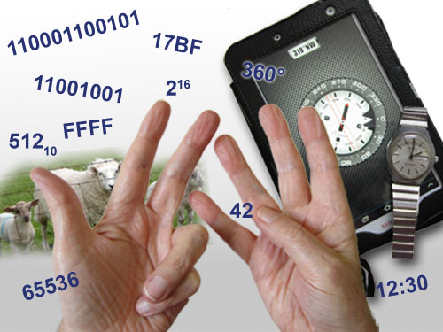
Why so many Number Systems?
Ask most people what the most commonly used number system is, and they would probably reply (after a bit of thought), the decimal system. But actually many number systems, and counting systems are used, without the users thinking much about it. For example clocks and compasses use the ancient Babylonian number system based on 60 rather than the decimal system based on 10. Why? Because 60 is easier to divide into equal segments, it can be evenly divided by 1,2,3,4,5,6,10,12,15, 20 and 30. This is much better for applications such as time, or degrees of angle than a base of 10, which can only be divided into equal parts by 1, 2 and 5.
Many counting systems are ancient in origin and are still in use because they are useful for particular purposes.
Using the decimal system it is easy to count up to ten fingers, using just the fingers on two hands. In northern Britain farmers, for centuries, used an ancient Celtic counting system, based on 20 (also called a score), to count their animals, and its use still persisted even into the second half of the twentieth century.
The binary system, based on 2, is just another special number system, and is used by digital electronic devices because digital circuits work on an electrical ‘on or off’ two state system, a number system based on 2 is therefore much easier for electronic devices to use. However binary is not a natural choice for human counting or calculation.
This module explains how binary, and some other number systems used in electronics work, and how computers and calculators use different forms of binary to carry out calculations. The important thing about this module is to get you to think about how the number systems work .
Binary Coded Decimal (BCD)
Representing Decimal Numbers
When calculations are carried out electronically they will usually be in binary or twos complement notation, but the result will very probably need to be displayed in decimal form. A binary number with its bits representing values of 1, 2, 4, 8, 16 etc. presents problems. It would be better if a particular number of binary bits could represent the numbers 0 to 9, but this doesn’t happen in pure binary, a 3 bit binary number represents the values 0 to 7 and 4 bit represents 0 to 15. What is needed is a system where a group of binary digits can represent the decimal numbers 0-9, and the next group 10-90 etc.
To make this possible, binary codes are used that have ten values, but where each value is represented by the 1s and 0s of a binary code. These special ‘half way’ codes are called BINARY CODED DECIMAL or BCD. There are several different BCD codes, but they have a basic similarity. Each of the ten decimal digits 0 to 9 is represented by a group of 4 binary bits, but in codes the binary equivalents of the 10 decimal numbers do not necessarily need to be in a consecutive order. Any group of 4 bits can represent any decimal value, so long as the relationship for that particular code is known.
In fact any ten of the 16 available four bit combinations could be used to represent 10 decimal numbers, and this is where different BCD codes vary. There can be advantages in some specialist applications in using some particular variation of BCD. For example it may be useful to have a BCD code that can be used for calculations, which means having positive and negative values, similar to the twos complement system, but BCD codes are most often used for the display of decimal digits. The most commonly encountered version of BCD binary code is the BCD8421 code. In this version the numbers 0 to 9 are represented by their pure binary equivalents, 4 bits per decimal number, in consecutive order.
BCD Codes
The BCD8421 code is so called because each of the four bits is given a ‘weighting’ according to its column value in the binary system. The least significant bit (lsb) has the weight or value 1, the next bit, going left, the value 2. The next bit has the value 4, and the most significant bit (msb) the value 8, as shown in Table 1.6.1.

So the 8421BCD code for the decimal number 610 is 01108421. Check this from Table 1.6.1.
For numbers greater than 9 the system is extended by using a second block of 4 bits to represent tens and a third block to represent hundreds etc.
2410 in 8 bit binary would be 00011000 but in BCD8421 is 0010 0100.
99210 in 16 bit binary would be 00000011111000002 but in BCD8421 is 1001 1001 0010.
Therefore BCD acts as a half way stage between binary and true decimal representation, often preparing the result of a pure binary calculation for display on a decimal numerical display. Although BCD can be used in calculation, the values are not the same as pure binary and must be treated differently if correct results are to be obtained. The facility to make calculations in BCD is included in some microprocessors.
One of the main drawbacks of BCD is that, because sixteen values are available from four bits, but only ten are used, there are several redundant values whichever BCD system is used. This is wasteful in terms of circuitry, as the fourth bit (the 8s column) is under used.
Try some simple conversions between Decimal and BCD8421
32110 to BCD8421
6523110 to BCD8421
001101110110 BCD8421 to decimal.
0011001011000110 BCD8421 to decimal.

Fig. 1.6.1 Seven Segment Display
Display Decoder/Drivers
Depending on the type of display some further code conversion may also be needed. One popular type of decimal display is the 7 segment display used in LED and LCD numerical displays, where any decimal digit is made up of 7 segments arranged as a figure 8, with an extra LED or LCD dot that can be used as a decimal point, as shown in Fig 1.6.1. These displays therefore require 7 inputs, one to each of the LEDs a to g (the decimal point is usually driven separately). Therefore the 4 bit output in BCD must be converted to supply the correct 7 bit pattern of outputs to drive the display.

Fig. 1.6.2 Driving a 7 Segment Display
The four BCD bits are usually converted (decoded) to provide the correct logic for driving the 7 inputs of the display by integrated circuits such as the HEF4511B BCD to 7 segment decoder/driver from NXP Semiconductors and the 7466 BCD to 7 segment decoder.

Question
BCD to 7 segment decoders implement a logic truth table such as the one illustrated in Table 1.6.2. There are different types of display implemented by different types of decoder, notice in table 1.6.2 that some of the output digits* may be either 1 or 0 (depending on the IC used). Why would this be, and what effect would it have on the display?
Notice that the 4 bit input to the decoder illustrated in Table 1.6.2 can, in this case, be in either BCD8421 or in 4 bit binary as any binary number over 9 will result in a blank display.
Alternative BCD Codes

Although BCD8421 is the most commonly used version of BCD, a number of other codes exist using other values of weighting. Some of the more common variations are shown in Table 1.6.3. The weighting values in these codes are not randomly chosen, but each has particular merits for specific applications. Some codes are more useful for displaying decimal results with fractions, as with financial data. With others it is easier to assign positive and negative values to numbers. For example with Excess 3 code, 310 is added to the original BCD value and this makes the code ‘reflexive’, that is the top half of the code is a mirror image and the complement of the bottom half, 5211 code is also self-complementing in this way. Some values in these BCD codes can also have alternative 1 and 0 combinations using the same weighting and are designed to improve calculation or error detection in specific systems.
Gray Code

Fig. 1.6.3 Four Bit Gray Code Disk
Binary codes are not only used for data output. Another special binary code that is extensively used for reading positional information on mechanical devices such as rotating shafts is Gray Code. This is a 4 bit code that uses all 16 values, and as the values change through 0-1510 the code‘s binary values change only 1 bit at a time, (see Table 1.6.4). The binary values are encoded onto a rotating disk (Fig. 1.6.3) and as it rotates the light and dark areas are read by optical sensors.
As only one sensor sees a change at any one time, this reduces errors that may be created as the sensors pass from light to dark (0 to 1) or back again. The problem with this kind of sensing is that if two or more sensors are allowed to change simultaneously, it cannot be guaranteed that the data from the sensors would change at exactly the same time. If this happened there would be a brief time when a wrong binary code may be generated, suggesting that the disk is in a different position to its actual position. The one bit at a time feature of gray code effectively eliminates such errors. Notice also that the sequence of binary values also rotates continually, with the code for 15 changing back to 0 with only 1 bit changing. With a 4 bit coded disk as illustrated in Fig. 1.6.3, the position is read every 22.5° but with more bits, greater accuracy can be achieved.
Introduction Logic Families
the differences and similarities between the various families of logic ICs available are described, along with their important operating conditions.
Logic 1 and Logic 0 are a bit more complex that 5V and 0V because these digital ICs are really little analogue circuits posing as ‘Digital’. A sort of sheep in wolves clothing!
Find out how logic gates actually work, and learn about the parameters that govern how the chips should be used. Special versions of the basic logic gates are also explained, such as Schmitt gates, open collectors, and buffers.
The 74 series of logic ICs introduced in this module, has been the backbone of digital electronics for about the last 50 years. Although nowadays they have been replaced in many applications by bigger, faster smarter chips, the 74 series families continue to play an important role in electronics, and learning about them is a sound basis for understanding the vital basics of digital electronics.
Logic Families Compared
Power, Speed and Compatibility
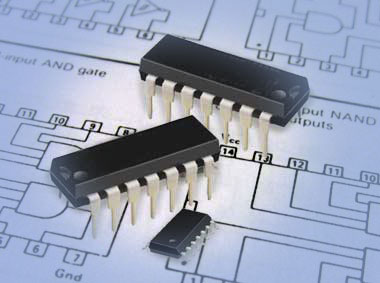
The logic gates are available in different combinations within I/C packages. As well as the basic logic functions, compatible ICs are available, which contain particular useful combinations of gates providing a convenient way of constructing more complex circuits. Hundreds of different, but directly inter-connectable logic ICs are available. The most commonly available logic ICs are the 74 series family and its sub−families, identifiable because their type numbers all start with the number 74.
the number 74.

Fig.3.1.1 Logic IC Device Numbering
74 Series Device Identification
A typical 74 series IC is shown in Fig 3.1.1 and can be identified by the number MC74HC04N, which is a common structure for 74 series logic ICs, which breaks down into several sections as follows:
MC − One to three letter manufacturer’s ID code. (e.g. National Semiconductor/Texas Instruments)
74 − Commercial grade, IC plastic package with temperature range of 0°C to +70°C although some sub families have an extended range of − 40°C to +125°C.
(Also 54 Military/Aerospace grade, IC ceramic package with temperature range of −55°C to +125°C).
HC − Two to three letter code indicating sub-family (HC = High speed CMOS, HCT = High speed CMOS, TTL compatible).
04 − Two to four digit type number, indicates the type of circuit or gates with IC. 04 = Hex (6 per IC) Inverters.
N − One or two letter code for package type, e.g. N = DIP - Dual Inline Package. The codes used vary between manufacturers, but package details are usually included on the IC datasheet.
Compatibility between Logic ICs
The use of a single family within a circuit design with direct connections between ICs enables circuit designers to produce circuits consisting mainly of ICs, with few extra coupling or biasing components. This greatly reduces the component count of a circuit, which among other benefits, reduces size and increases reliability.
ICs of a particular family generally use a common technology, but ICs in other families, using different technologies, usually have different input and output requirements, different supply voltages, and other parameters that affect the use of digital ICs. Making direct connections between ICs of a single family or sub family is usually very simple. ICs of different families can sometimes also be directly connected together, but may require some extra circuitry at the interface of the two IC families to maintain compatibility.
Why these different families exist dates back to the 1960s when groups of logic ICs using different technologies first became available.
Scale of Integration

Fig. 3.1.2 Original CMOS and TTL Pinouts for Comparable NAND gate ICs
RTL (resistor-transistor logic) and DTL (diode-transistor logic), successfully used in early computers were superseded by TTL (transistor-transistor logic), which became the dominant technology. However as these ICs developed, at first as SSI (small scale integrated) devices, with just a few transistors per chip, and then as MSI (medium scale integrated) devices with 100 or more transistors, a problem arose that as more gates (and therefore more transistors) were packed into a single IC, the scale of integration would be limited by the power dissipation of the device.
Although each gate only dissipates a few milliWatts, the heat generated within a single large-scale integrated (LSI) circuit containing tens of thousands of transistors could potentially quickly destroy the IC.
It was therefore necessary to develop gates with much lower power consumption, so in the 1970s a series of CMOS (Complimentary Metal Oxide Semiconductor) ICs, called the 4000 series was developed, in which the power consumed by each gate was about 1/1000th of the power consumed by a similar TTL gate, making very large scale integration (VLSI) with millions, and more recently billions of transistors per chip possible. CMOS chips were also more flexible in their supply voltage requirements, working from supplies between 3V to 18V, compared with the TTL requirement for supplies of 5V +/- 0.25V. This made CMOS devices ideal for battery operation. However the speed at which these early CMOS devices operated was about 10 times slower than TTL.
These two logic families were not readily compatible; apart from the differences in supply voltage and speed, they were not particularly pin compatible, as illustrated in Fig. 3.1.2 so TTL chips, even simple ICs with the same types of gates as CMOS, could not be directly interchanged.
Power vs. Speed
Ideally logic gates should be able to change state immediately and consume little or no power. However the laws of physics, as presently understood, say that this is not possible. All electrical circuits must consume some power, and any change in the voltages and currents in that circuit must take at least some time.
Chip designers therefore had to try and reconcile the fact that higher speeds meant more power consumption, and so some families developed, using optimum speed whilst others were developed to use the minimum of power.
CMOS (Complimentary Metal Oxide Semiconductor) chips, designed for minimum power, got faster and TTL families, using bipolar transistors for optimum speed, were developed that not only increased speed but also reduced power consumption.

Fig 3.1.3 Logic Families Power vs Speed
As the overall performance of these families increased they also became more compatible. The increase in portable (battery powered) electronic devices along with the ability of chip manufacturers to make the component parts of ICs much smaller also meant that power could be reduced and speed increased.
Some of the main TTL and CMOS sub-families currently in use are compared in Fig. 3.1.3. Note how CMOS speed has been increased and power reduced with the introduction of the 74HC (High-speed CMOS) although (as the laws of physics demand), power consumption still increases, as the frequency at which they operate increases.
Because CMOS and TTL families can now operate at similar speeds and similar power consumption, the 74HCT (a CMOS sub-family compatible with TTL pinouts and voltage levels) now makes it possible to easily interface both families within in a single design, so enabling the use of the best features of each family.
74HC (and 74HCT for interfacing with the larger 74TTL families) are now recommended for most new designs.
The ECL Families
The ECL (Emitter Coupled Logic) families, originated in the late 1950s and remain the fastest chips available, but consume more power, and because they use a negative power supply (of −5.2V) have been difficult to interface with other families. This has changed with the introduction of PECL (Positive ECL) using a +5V supply, and LVPECL (Low Voltage Positive ECL) using a +3.3V supply. This now offers the opportunity of using mixed CMOS and TTL families at various power levels for logic operations and interfacing with ECL for high frequency digital communications.
How Logic Gates Work

Fig 3.2.1 Typical Logic IC Packages
Logic Technologies
Small and medium scale (SSI and MSI) Logic IC families are currently made in a wide range of sub-families and a variety of package types, using three basically different technologies:
• TTL (Transistor Transistor Logic)
• CMOS (Complimentary Metal Oxide Semiconductor)
• ECL (Emitter Coupled Logic)
Transistor Transistor Logic (TTL)
TTL gates use a 5V(±0.25V) supply, and are capable of high-speed operation. Over 600 different logic ICs are available, covering a very wide range of digital functions. Due to the use of bipolar transistors, TTL has much higher power consumption than similar CMOS types, when working at relatively low frequencies. As the frequency of signals handled increases however, this difference decreases as the power consumption of CMOS increases and TTL power consumption remains nearly constant.
TTL NAND Gate Operation

Fig. 3.2.2 Schematic diagram of a TTL NAND Gate
Notice that this circuit looks similar to those found in analogue push pull amplifiers, except that the transistors here are driven either into cut-off or saturation, rather than working in their linear operating condition. Also, being constucted within an IC, it can use a device not normally found in conventional analogue amplifiers, a multi emitter transistor.
Fig. 3.2.2 shows a typical schematic for a TTL NAND gate. R1 is a low value resistor (about 4K) and as the base current of T1 is small, the base voltage is about +5V. If both emitters of T1 are at logic 1, (also around +5V), there will be very little potential difference between base and emitter, and T1 will be turned off. As T1 is not conducting, its collector will also be at about 5V, and due to this high potential, T2 base will have a higher potential than its emitter, which will cause T2 to conduct heavily and go into saturation.
T2 collector will therefore fall to a low potential, and the emitter voltage of T2 will rise due to the current flow through R3. The voltage across R3 will rise to a sufficient level (about 0.7V) to fully turn on T3. As T3 saturates, its collector voltage will fall to about 0.2V, thus giving a logic 0 state at the output terminal.
T4 emitter voltage is made up of T3 VCE (about 0.2V) plus the forward voltage drop across D1, which will be about 0.7V, giving an emitter potential of 0.2V + 0.7V = 0.9V, the same as its base voltage.
The base potential of T4 is made up of T3 base/emitter potential VBE (about 0.7V), plus the collector/emitter, potential (VCE) of T2, (about 0.2V), giving a base voltage for T4 of about 0.9V. Therefore the base and emitter voltages on T4 are approximately equal, so T4 will be turned off.
With BOTH input terminals are at logic 1 therefore, the output terminal will be at logic 0, the correct operation for a NAND gate.
If either one of the inputs is taken to logic 0 however, this will make T1 conduct, as the emitter that is at logic 0 will be at a lower voltage than that supplied to the base by R1. This will cause T1 to saturate, taking its collector to a low potential (less than 0.8V) and as this is also connected to T2 base T2 will turn off, making its collector voltage and T4 base voltage, rise to very nearly +Vcc.
As virtually no current (ICE) is flowing through T2 collector/emitter circuit, practically no voltage is developed across the emitter resistor R3, reducing T3 base voltage to 0V, and so T3 is turned off. However, sufficient current will be flowing out of the output terminal (feeding the next gate input circuit) to cause T4 emitter to be held at about 4.1V. This is 0.9V below +Vcc, made up of the voltage across D1 (0.7V) plus the saturation voltage VCE of T4 (0.2V). This places about 4V or logic 1 (between 2.4V and 5V) on the output terminal.

Fig. 3.2.3 CMOS NAND Gate
Complimentary Metal Oxide Semiconductor (CMOS)
CMOS ICs can operate from a wide range of supply voltages (typically 3 to 18V, and lower with some sub families), with very low power consumption. The name CMOS (COMPLIMENTARY Metal Oxide Semiconductor) is used because opposite types, both P type and N type MOSFETs are used in the construction of these gates. Fig 3.2.3 shows a theoretical schematic circuit for a NAND gate.
CMOS NAND Gate Operation
T1 and T2 are P channel MOSFETs and either of these transistors will be turned on when logic 0 is applied to its gate. T3 and T4 are N channel MOSFETs and either of these transistors will be turned on by applying a logic 1 to its gate.
T1 and T2 are connected in parallel from supply to the output X, so switching either of them on will result in a logic 1 at output X.
T3 and T4 are connected in series between X and ground so when both are switched on, a logic 0 will appear at output X. The eventual logic state at X depends of course on the on or off state of the combination of all four transistors, and these are controlled by the logic states applied to the inputs A and B as can be seen in Table 3.2.1.
Input A controls T2 and T3 so that when logic 0 is applied, T2 is on and T3 is off. Logic 1 on input A reverses this condition.
Input B controls T1 and T4 so that logic 0 applied to B turns T1 on and T4 off. Logic 1 on input B reverses the condition.

Anti-Static Protection
Because MOSFETs, have a gate that is insulated from the transistor’s conducting channel, they can also be called Insulated Gate Field Effect Transistors (IGFETs) and have practically no current flowing into their inputs, therefore any high voltages due to static electricity are not reduced by current flow so can easily destroy the very thin insulating layer between the gate and the conducting channel of the transistor. To minimise such damage and protect the gates from any high voltage static electricity spikes that may appear across the IC during handling, CMOS ICs should always be stored in anti static packaging, and handled in accordance with manufacturers handling procedures.

Fig. 3.2.4 Anti Static Packaging
To protect the ICs from high voltage spikes when in circuit, protection diodes (see Fig. 3.2.3) are used at the gate inputs. Protection diode D3 is connected between input A and +Vcc so that if any voltage higher than Vcc appears at input A, D3 will become forward biased and conduct, limiting the input voltage to +Vcc.
Similarly, if a negative voltage appears at input A, D4 will conduct, limiting the input voltage to no less than 0V.
Input B is protected in a similar manner by D1 and D2. Note however, that although the diodes offer protection, it is still possible that very large static voltages may still damage these devices, so anti-static precautions should always be used when handling CMOS devices.
Capacitance in CMOS devices
Because CMOS transistors are IGFETs with insulating layers between electrodes, they naturally act as capacitors. The value of these capacitors is of course small because the electrodes either side of the insulating layer are extremely small. However the combined capacitance between the various sections of the several IGFETs that make up a CMOS gate, added to any capacitance between lead-out wires etc. is sufficient to have an effect on the overall gate performance. When a change in logic state occurs, ideally it should complete its transition from 0 to 1, or 1 to 0 immediately. However because of the gate capacitance and internal resistances that are present, the change cannot happen in less time than the CR time constant of the circuit. The output of a gate cannot complete its change until the input has completed its transition, and the output must similarly take some additional time, before reaching its new value.

Fig. 3.2.5 Propagation Delay
Propagation Delay
Any gate introduces some delay between when its input changes and when a resulting change takes place at its output. This is called the propagation delay of the gate, and is made up of two, often different delays, as shown in Fig. 3.2.5 using a simple inverter gate as an example.
The High to Low Propagation Time (tPHL) is measured from the time (usually in nanoseconds) when the input rises past the 50% level, to the time when the output falls past the 50% level. A similar, but usually longer delay (tPLH) is measured from when the input falls past the 50% level, to when the output rises past the 50% level. Therefore the average propagation delay of the gate is:
(tPHL + tPLH) / 2
Typical average propagation delay for a 74HC04 inverter is about 8ns.
Emitter Coupled Logic (ECL)

Fig. 3.2.6 ECL OR/NOR Gate
Because the early designs of ECL ICs needed a negative supply voltage of -5.2V they were not particularly compatible with either CMOS or TTL circuits, even though, like TTL, they use bipolar transistors. However there are now newer ECL sub families available that use positive supplies such as PECL (+5V) and LVPECL (+3.3V). Although the supply voltages for these ECL gates are now more compatible with CMOS and TTL, the logic levels used in ECL are quite different to other logic families. ECL is extremely fast in operation with propagation delays of less than 1 nanosecond available.
ECL was extensively used in early super computers, but because of its high power requirement (up to 40mW per gate) fell out of general use. Today modern ECL sub families such as PECL or LVPECL are now mainly used for interfacing CMOS or TTL digital systems to high frequency signal communication (up to several GHz) circuits. The two opposite logic state outputs (VOUTand VOUT) means that the ECL OR gate illustrated in Fig. 3.2.6 can operate as an OR gate or a NOR gate and also makes ECL ideal for interfacing with differential (two conductor) transmission lines possible. This method of transferring high speed digital data uses a pair of high frequency anti-phase signals as a method of cancelling out electromagnetic interference that may be picked up during transmission.
Operation
The basis of the ECL circuit is a differential amplifier (T3 and T4 in Fig. 3.2.6), which is ideal for high frequency use and reducing noise on the amplified signals. This amplifier compares the voltage at the inputs (the bases of T1 and T3) with a steady reference voltage produced by T5, D1 and D2. To avoid any delay caused by the transistors saturating, the differential amplifier is designed to always be in a linear amplifying mode, approximately half way between saturation and cut off.
The voltage change between logic 1 and logic 0 is between −0.9 and −1.75 respectively. Power consumption is considerably higher than CMOS or TTL because the transistors in the differential amplifier are always conducting, rather than switching on and off as in TTL and CMOS.
ECL and PECL use differential transmission, a pair of conductors with opposite polarity signals, along which data can be transmitted for around 50m. The technique reduces interference in the transmission lines when passing data from one digital system to another, and was used in many data transmission links in computing up to the 1990s, but for many uses, such as USB, HDMI etc. ECL has now been largely superseded by LVDS (Low Voltage Differential Signalling), a CMOS based high frequency digital transmission system. This system uses much less power than ECL and can transfer data over distances of up to 10m at a rate of several hundred Megabits per second.
Logic IC Parameters
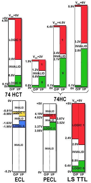
Logic 1 and Logic 0 are not simply 5V and 0V or even Vcc and Ground. Within any family of ICs the voltages and currents indicating 1 and 0 cover defined ranges unique to that logic family. The range of voltages allowed for a particular logic level depends on the amount of current flowing into or out of the logic gate inputs or output, the larger the current the output is supplying, the lower the output voltage will be.
Each output will supply a certain amount of current before the output voltage falls too far to be called logic 1, and each gate input will need to be supplied with a certain amount of current to raise the input voltage sufficiently to be recognised as logic 1.
Examples of typical logic levels at inputs and outputs in a range of logic families are illustrated in Fig. 3.3.1. These levels are fairly standard throughout a particular family, although there can be minor differences in these and other parameters, between products from different manufacturers. In addition there are sub families within these families that may have different defined levels. When designing digital circuits, or replacing ICs in critical equipment, it is therefore essential to consult the appropriate manufacturer’s data sheets.
Logic 1 levels for inputs and outputs are shown in red and logic 0 in green. To highlight the fact that true ECL gates, have negative logic levels, these colours have been changed to yellow and blue respectively.
Notice that the logic levels for outputs (left column) and inputs (right column) in all of the families are different. This ensures that provided that the output voltage of a gate is within its defined logic limits for 1 or 0, any compatible gate input connected to that output will recognise the correct 1 or 0 levels. The difference between levels at the output and input in any particular family is called the ‘Noise Margin’.

Fig. 3.3.2 Logic IC Decoupling
Noise Margin
Because voltages in digital circuits can be continually changing very rapidly between logic 1 and logic 0, (virtually between supply voltage and ground), they have the potential to produce a lot of noise, in the form of high frequency voltage spikes on the IC power supply lines.
To counteract this it is important to include effective decoupling, not only at the power supply unit, but also by connecting decoupling capacitors across the VDD and 0V connections at each IC. These capacitors are normally connected as physically close to the IC as possible, as shown in Fig. 3.3.2.

Fig. 3.3.3 Noise Margin
Despite these measures, it is possible that some noise will remain that could disturb the logic levels of digital signals. However logic ICs have a built in ‘Noise Margin’, illustrated in Fig. 3.3.3, This is the difference between the worst-case voltage ( VOH) for logic 1 at the output , which is 2.4V in the case of 74HCT, and the minimum voltage required for logic 1 to be recognised at the input (VIH), 2.0V in 74HCT. This difference (0.4V) should be enough to ensure that noise does not cause a wrong logic level to be seen by the 74HCT input; a similar noise margin is provided for logic 0 (VIL−VOL) as shown in Fig. 3.3.3.
It can be seen from Fig. 3.3.1 that different logic families have very different noise margins. The CMOS 74HC gates have a much wider noise margin than LS TTL or the TTL compatible 74HCT series, making them much more tolerant of noise. This is because the CMOS outputs are normally driven very close to VDD or 0V as very little current is drawn from a CMOS output to drive any CMOS inputs connected to it.
Minimising Power Consumption
In both CMOS and TTL ranges it is important that the central (white) range of voltages in Fig. 3.3.1 is avoided as much as possible. This is done by ensuring that switching between 1 and 0 is as fast as possible. If the IC is operating within the ‘invalid range’, power consumption increases dramatically. When the output voltage is close to the supply voltage, current is almost zero and therefore power (V x I) is very low. Similarly when the output is close to 0V but maximum current is flowing, V x I is again very low. Power consumption is at its highest when both voltage and current are around the mid range, and operating the ICs in this range would substantially increase the heat dissipated by the IC.
However, any unused inputs on CMOS ICs will tend to float to a mid voltage level, causing power dissipation to increase. To avoid problems with floating CMOS inputs, they should therefore be connected to either supply or ground, either directly or via a resistor, so they are not allowed to ‘float’ and cause excessive power consumption. This is not absolutely necessary, (though good practice), with TTL ICs as any unused TTL inputs will float up to logic 1.
Notice that ECL/PECL gates operate exclusively in this mid range area; this is why power consumption in these families is higher than in TTL or CMOS. However the close proximity of the logic 1 and logic 0 values in ECL allows for much higher switching speeds. This operation also gives ECL a much narrower noise margin however, making these chips more susceptible to noise. This is the reason for ECL having its positive supply tied to 0V, which is generally less noisy than sharing a positive supply with many other ICs.
Mixing Logic Families
The differences in the output voltage and/or current levels for TTL and the CMOS gates can affect circuit operation if both bipolar and CMOS logic families are used in the same circuit (e.g. LS TTL and HCT or CMOS), or if an older TTL IC is replaced by an ‘equivalent’ HCT chip during repairs or upgrading.
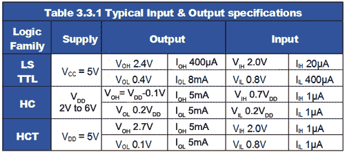
When mixing logic families it is important to consult input and output specifications such as those listed in Table 3.3.1 to ensure that the input and output conditions are compatible. The data in Table 3.3.1 shows typical input and output values for logic families, but particular ICs within a family or sub-family, and ICs from different suppliers will differ. The only way to be sure of complete compatibility is to consult the manufacturers data sheets for the ICs concerned.
Generally TTL outputs will interface to other TTL family inputs, and to 74HCT, which has TTL level inputs and CMOS level outputs.
The 74HCT outputs will interface to CMOS inputs provided both ICs are working from a common +VDD supply. This should not be a problem with the 74HC series, as it will operate on 5V supplies.

Fig. 3.3.4 Interfacing TTL to 74HC
Connecting a TTL output to a CMOS HC input may work if TTL input is not heavily loaded. A problem occurs however when more current is sourced by the TTL logic 1 output. Its output voltage (VOH) depends on the current being drawn from it and will vary from around 3.3V with no load current, down to about 2.4V when the output is sourcing around 400µA. As the HC gate input requires a minimum input voltage (VIH) of 3.2V there is a chance that at some output current between 0 and 400µA the TTL output will fall below 3.2V, and fail to be recognised as logic 1 by an HC input using its maximum supply voltage of 16V. Even if the HC supply is reduced to 4.5V there will still be a chance of mismatch.
The remedy is to fit a pull up resistor from the TTL output to Vcc as shown in Fig 3.3.4, which will increase the TTL output voltage (VOH) sufficiently to ensure correct interfacing. The value of the resistor should be between 1K and 2K ohms, the optimum value depending on the Fan out factor of the TTL gate and the number of gates being driven, the less current the output is sourcing, the lower the value of pull-up resistor needed.
Level Translation
With the older +5V TTL and +3V to +18V 4000 CMOS families the logic levels must be shifted considerably. For this purpose, a level translator IC such as the MC14504B from ON Semiconductor will provide level shifting for up to six ICs with VCC or VDD at any value between +0.5V and +18V. An alternative solution to level translation is to use Open Collector ICs.
ECL to TTL interfacing is carried out by ICs such as the MC10ELT25 from ON Semiconductor.
Sinking and Sourcing

Fig.3.3.5 Sinking and Sourcing
Because the output circuits of logic gates are a type of push-pull or ‘Totem Pole’ output with only one of its two output transistors conducting at any one time, when the output terminal is at logic 1 T4 is turned on the output terminal of Gate 1 will supply (or SOURCE) current via T4 and D1 to the input of Gate 2. This will cause gate 2 input to also be at its logic 1 state as shown in Fig. 3.3.5 (a).
When gate 1 output is at logic 0, T4 is turned off and T3 is turned on, and output current will now flow in the opposite direction, from the input of Gate 2 in Fig 3.3.5 (b) and via T3 collector and emitter to ground; this is called SINKING the current.
When a LS TTL gate output acts as a source, a maximum source current of -400µA is available to be drawn from the output terminal. Note that the minus sign used in this case signifies a current that is flowing FROM the gate output. When the output is sinking current, the LS TTL gate is able to sink 8mA. Notice the sink current has no minus sign as it flows into the output terminal.
Fan Out
A standard LS TTL gate is therefore able to sink 20 times the amount of current it is able to source. This ratio between sinking and sourcing current is typical with bipolar gates. The above conditions mean that the output of a standard LS TTL gate is capable of driving up to 20 LS TTL inputs without its output voltage falling below the minimum specified for logic 1. This is described as a FAN OUT FACTOR of 20, but each logic family has its own particular ratio of sinking to sourcing currents, so the fan out factor of 20 is only correct where a standard LS TTL gate is driving one or more gates of the same (LS TTL) family.
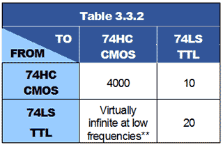
Because gates of other families have different input and output currents the actual fan out factor will be different when logic families are mixed within a circuit. For example, Table 3.3.2 shows how mixing LS TTL and CMOS HC gates affects their fan out factors.
A 74HC output can feed up to 4000 74HC inputs, because the input currents of 74HC gates are extremely low, but only 10 74LS TTL inputs.
A Standard LS TTL gate output can drive up to 20 LS TTL inputs, but one LS TTL gate output can drive a virtually infinite number of 74HC CMOS gates because of the low current requirement of 74HC CMOS gates.
High Frequency AC Fan Out **
However, although a standard LS TTL output will apparently feed an infinite number of 74HC inputs (** in Table 3.3.2), when high frequency signals are used, additional limits need to be considered. Each CMOS input and output has a capacitance of several pF, and if a CMOS output is to feed a number of inputs, the individual input capacitances are in effect connected in parallel (and so add) to form a larger capacitance across any output driving the CMOS inputs.
The effect of this capacitance, as well as any capacitance due to connecting lines on the printed circuit board will combine with the output impedance of the gate to form a low pass filter. The effect of this filter will be to remove some of the higher frequencies in the signal, increasing rise and fall times, lengthening propagation delay and potentially causing timing errors in the system, therefore large fan outs are best avoided. These effects make the design of high-speed digital systems similar in some respects to high frequency RF circuits where stray capacitance, cable routing and interference play a large part in the circuit design.
Special Purpose Logic ICs
Open Collector Gates
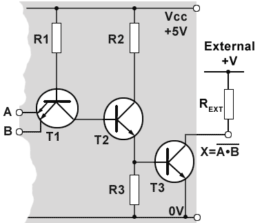
Fig. 3.4.1 shows the internal circuit of an open collector NAND gate. The grey area illustrates a single gate within an IC. Instead of the normal Totem Pole output stage, the single output transistor T3 has its collector brought out to an external pin, which can be connected to an external power supply, at a different voltage to the VCC supply of the IC, via an external load resistor REXT.
In Fig. 3.4.1, when both inputs A and B are at logic 0, the high voltage applied to T1 base will cause it to turn on, so that T1 collector will go to near 0V and T2 will turn off.
As T2 is off there will be virtually no current through R3 so the voltage at T3 gate will be around 0V. T3 will therefore be turned off and the external pull up resistor REXT will pull the collector voltage of T3 up to +V, which will be at the valid logic 1 level of the next gate.
Logic Level Translation
Open collector and open drain gates can therefore be used for changing the levels of an output to match the higher or lower logic levels of an input on a different family of gates, when gates of mixed families are used.
Open collector gates can be used with external collector VCC supplies having a voltage typically somewhere between +1.5V to +5.5V for logic gates, Buffer ICs are also available that can operate on collector VCC supplies up to +30V. The maximum value of collector voltage is set by the VOH parameter of the open collector gate.

Fig 3.4.2 Wired AND Function
Wired Logic Functions
Open collector ICs are available in most of the logic types, AND, NAND etc, with the exception of OR gates. However open collector gates can be used to make both wired AND and wired OR functions as shown in Figs. 3.4.2 and 3.4.3. The outputs of gates without open collectors must not be connected together, because if the outputs happen to be at opposite logic states, the gate with a logic 0 output will try to sink more current than the logic 1 gate can source, and damage will most probably occur. However with open collector (or drain) gates, a gate output at logic 0 will be sinking current drawn from the external pull up resistor REXT, and any other connected open collector gate trying to output a logic 1 will have its output transistor turned off and so will not be sourcing any current.
Wired AND
If two or more open collector gate outputs are connected together, any gate with a logic 0 output will pull all other connected outputs to logic 0, giving an output of logic 0 at output X, but if all the connected outputs are at logic 1, then X will be at logic 1, the action of an ‘invisible’ AND gate.

Fig 3.4.3 Wired OR Function
Wired OR
It is also possible to implement a wired OR function using open collector (or drain) gates as shown in Fig. 3.4.3, although the explanation here is a little more complex as it involves using Negative Logic.
The circuit in Fig. 3.4.3 is used to obtain the Boolean function (A•B)+(C•D) without using a physical OR gate.
Notice that the circuit in Fig. 3.4.3 is similar to the wired AND circuit in Fig. 3.4.2, except that the two open collector AND gates have been replaced by two open collector NAND gates. The main difference with this circuit however is that to obtain an OR function from what appears to be a wired AND function, Negative Logic is applied.

Fig 3.4.4 Active Zero
Negative Logic
In Digital Electronics it is usual to explain the operation of a circuit theoretically in terms of 1 and 0, but the actual gates are really just specialised analogue circuits. As explained in Module 3.3, the outputs normally thought of as 1s and 0s are really ranges of voltage and current, 1 and 0 are no more than convenient names given to these voltages and currents. It is also usually assumed that logic 1 refers to the higher of the two voltage ranges − but that need not be so! Also logic 1 is normally the active state of an output, and logic 0 is the inactive state, but this is not always what is required.
The source current available from an open collector gate output when it is at logic 1 is very small, compared to the current the gate will sink when its output transistor is turned on, giving an output of logic 0.
It is quite reasonable therefore, to drive some output device, such as a lamp or relay for example, using the higher current available from a logic 0 output, as shown in Fig. 3.4.4.

In negative logic it is assumed that the active state is the low voltage state and that this is called logic 1. What this does to the familiar truth tables used in positive logic is to replace all the logic 1s (previously assumed to be the active state) with logic 0s and vice versa.
The effect of this reversal of logic states can be seen in Table 3.4.1. The X column for the positive AND gate is as would be expected; a logic 1 when both A and B are 1, otherwise logic 0s. However using negative logic on the same physical AND gate, simply swapping the 1s and 0s in both the input and output columns has changed the X output column from three 0s and a 1, to three 1s and a 0, so that X = 1 whenever A or B is 1. The AND gate has been transformed to an OR gate!
Using negative logic will change the function of any of the six two input logic gates, if you want to see what happens, try re-writing the truth tables for AND, OR, NAND, NOR, XOR, and XNOR in a similar manner to Table 3.4.1. However, negative logic is not widely used and so unless a logic circuit is actually described as using negative logic, it can be assumed that positive logic is being applied.

Fig. 3.4.5 How the Wired OR Circuit Works
Negative Logic and the Wired OR Circuit
Fig. 3.4.5 shows how the wired AND circuit shown in Fig. 3.4.2 is made to work as the wired OR in Fig. 3.4.3. The only physical change is that the two AND gates have been replaced by two NAND gates; this has the effect of inverting the inputs of the ‘invisible’ wired AND gate. According to De Morgan’s Theorem, this has the effect of converting an AND gate into a NOR gate.
To implement negative logic however, and change the invisible AND gate to an OR gate, both the inputs and the outputs must be inverted, changing all the 1s to 0s and 0s to 1s. The inversion ‘bubble’ is shown at the output of the wired OR gate because the active state of the output is chosen to be the low voltage output normally called the logic 0 inactive state, but now using negative logic as shown in Fig. 3.4.5, the low voltage output is considered to be the ‘active logic 1’ state using negative logic.
If positive logic is used however, and logic the low voltage output from the invisible wired AND gate called the inactive logic 0 state, the output of the wired gate is logic of the circuit is that of a wired NOR gate.

Fig 3.4.6 Open Collector/Drain Buffer ICs
Buffers
Buffers in digital electronics are special gates inserted between one circuit and another to reduce any unwanted interaction between the two. The gates in buffer ICs typically have high impedance inputs and low impedance outputs, giving larger fan out factors than standard gates. Another common use is to enable a logic circuit having a low voltage and/or low current output to drive a circuit or output device requiring higher voltage or current than is available for standard logic ICs.
Open Collector Buffers
Typical ICs using buffered output gates are shown in Fig. 3.4.6. Buffered inverters and non-inverters are common, but there are also gates with other logic functions that have buffered outputs, including some open collector gates, such as the 74HC03 Quad 2 input NAND with open drain from NXP Semiconductors.
Open collector buffers such as the SN74LS06 Hex inverter buffer/driver IC, and the non-inverting buffer SN7407 from Texas Instruments, allow devices such as lamps, motors and relays for example, that normally require higher currents and voltages, to be driven directly from a low voltage logic circuit.
Schmitt Gates

Fig. 3.4.7 Schmitt Gates
The digital signals processed by logic gates need to have fast rising and falling edges. Taking too much time to change logic states, spending too long in the ‘invalid’ zone between states, can cause unreliable logic levels, timing problems and excessive power dissipation, even shortening the life of logic ICs. Standard gate inputs change from 0 to 1 or 1 to 0 at a voltage of about 2.0V. If there is any noise on the input signal, it may be rapidly changing its voltage above and below this level, so causing the gate to rapidly change state if the noise exceeds the noise margin. These rapid and uncertain changes in the gate’s input circuit will also cause the output to oscillate between 1 and 0, transmitting the problem to any subsequent gates in the digital system.
To avoid these problems, gates with Schmitt inputs such as those shown in Fig. 3.4.7 are often used, especially at the input to a system where noise may be expected, as signals arrive from an external source.
Schmitt gates use positive feedback, which causes the gate to switch between logic states extremely quickly. They also have a hysteresis effect, which only allows a change of state to occur as the input voltage passes two specific and different voltages, the Positive-going input threshold voltage (VT+) and the Negative-going input threshold voltage (VT-).

Fig. 3.4.8 Schmitt Gate Action
As the input voltage passes VT+ during a positive going transition, the gate input changes very rapidly to its high state. It then cannot return to its low state until the input voltage falls to the lower level of VT-.
This action has several beneficial effects on poor input signals, as illustrated in Fig. 3.4.8.
(a) It can be used to change slowly changing signals to square waves having very fast transitions.
(b) Noise can be removed from signals, provided that the amplitude of the noise is not greater than ΔVT.
(c) Slow rise and fall times can be restored to practically instant transitions by feeding the signal through a Schmitt trigger.
74 Series Schmitt Gates
Typical Schmitt Hex inverter and Quad NAND gate ICs from the 74 series are illustrated in Fig. 3.4.9.

Fig 3.4.9 Schmitt Input ICs
Sequential Logic
Introduction
The logic circuits discussed in Digital Electronics Module 4 had output states that depended on the particular combination of logic states at the input connections to the circuit. For this reason these circuits are called combinational logic circuits.
Use Module 5 to learn about digital circuits that use SEQUENTIAL LOGIC.
In these circuits the output depends, not only on the combination of logic states at its inputs, but also on the logic states that existed previously. In other words the output depends on a SEQUENCE of events occurring at the circuit inputs. Examples of such circuits include clocks, flip-flops, bi-stables, counters, memories, and registers. The actions of these circuits depend on a range of basic sub-circuits.
Clock Circuits

Module 5.1 deals with clock oscillators, which are basically types of square wave generators or oscillators that produce a continuous stream of square waves or a continuous train of pulses (a "square" wave whose mark to space ratio is NOT 1:1). These pulses are used to sequence the actions of other devices in the sequential logic circuit so that all the actions taking place in the circuit are properly synchronised.
Bi-Stable Logic Devices

Bi-stable devices (popularly called Flip-flops) described in Modules 5.2 to 5.4, are sub-circuits, usually contained within ICs, and are the most basic type of 1-bit memory. They have outputs that can take up one of two stable states, Logic 1 or logic 0 or off. Once the device is triggered into one of these two states by an external input pulse, the output remains in that state until another pulse is used to reverse that state, so that a logic 1 output becomes logic 0 or vice versa. Again the circuit remains stable in this state until an input signal is used to reverse the output state. Hence the circuit is said to have Bi (two) stable output states.

Counters
Various types of digital counters are described in Module 5.6. Consisting of arrangements of bi-stables, they are very widely used in many types of digital systems from computer arithmetic to TV screens, as well as many digital timing and measurement devices.

Registers
Also consisting of arrays of bi-stable elements, the shift registers described in Module 5.7 are temporary storage devices (memories) for multi-bit digital data. The data can be stored in the register either one bit at a time (serial input) or as one or more bytes at a time (parallel input).
The register can then output the data in either serial or parallel form. Shift registers are vital to receiving or transmitting data in digital communications systems. They can also be used in digital arithmetic for operations such as multiplication and division.

A Simple ALU
A simple arithmetic and logic unit (ALU) is described in Module 5.8 and combines many of the combinational and sequential logic circuits described in modules 4 and 5 to demonstrate how a very complex application is built by combining a number of much simpler digital sub circuits.
Clocks and Timing Signals
Most sequential logic circuits are driven by a clock oscillator. This usually consists of an astable circuit producing regular pulses that should ideally:
1. Be constant in frequency
Many clock oscillators use a crystal to control the frequency. Because crystal oscillators generate normally high frequencies, where lower frequencies are required the original oscillator frequency is divided down from a very high frequency to a lower one using counter circuits.
2. Have fast rising and falling edges to its pulses.
It is the edges of the pulses that are important in timing the operation of many sequential circuits, the rise and fall times are usually be less than 100ns. The outputs of clock circuits will typically have to drive more gates than any other output in a given system. To prevent this load distorting the clock signal, it is usual for clock oscillator outputs to be fed via a buffer amplifier.
3. Have the correct logic levels
The signals produced by the clock circuits must have appropriate the logic levels for the circuits being supplied.
Simple Clock Oscillator

Fig. 5.1.1 Simple Schmitt Inverter Clock Oscillator
Fig 5.1.1 is probably the simplest oscillator possible, having only three components. Notice that the gate is a Schmitt inverter. This device has an extremely fast change over between logic states. Also the level at which it responds to an input change from 0 to 1 (Vt+) is higher than the level at which it changes from 1 to 0 (Vt-). The operation of the circuit is as follows.
Suppose the gate input is at logic 0, because the gate is an inverter, the output must be at logic 1, and C will therefore charge up via R from the output. This will happen with the normal CR charging curve. Once Vt+ is reached at the gate input, the gate output will rapidly switch to 0. The resistor is now connected effectively between the positive plate of C and zero volts. Thus the capacitor now discharges via R until the gate input voltage reduces to Vt- when the output will change to logic 1 once more, starting the charging and discharging cycle over again.
Fig. 5.1.2 Typical Basic Schmitt Oscillator Output
This Schmitt RC oscillator can produce a pulse waveform with an excellent wave shape and very fast rise and fall times. The mark to space ratio, as shown in Fig 5.1.2 is approximately 1:3.
The frequency of oscillation depends on the time constant of R and C, but is also affected by the characteristics of the logic family used. For the 74HC14 the frequency (ƒ)is calculated by:

When using the 74HCT14 the 0.8 correction factor is replaced by 0.67, however either of these formulae will give an approximate frequency. Whichever logic family is used, the frequency will vary with changes in supply voltage. Although this basic oscillator gives an excellent performance in many simple applications, if a stable frequency is an important factor in the choice of clock oscillator, there are of course better options.
Crystal Controlled Clock Oscillator

Fig. 5.1.3 Crystal Controlled Clock Oscillator
Fig. 5.1.3 uses three gates from a 74HCT04 IC, and a crystal to provide an accurate frequency of oscillation. Here, the oscillator is running at 3.276MHz but this can be reduced by dividing the output frequency down to a lower value by dividing it by 2 a number of times using a series of flip-flops.
The top waveform in Fig 5.1.4 shows the clock signal generated by Fig 5.1.3, and beneath it is the clock signal frequency divided by 4 after passing it through two flip-flops. Notice that after passing the signal through flip-flops, as well as being reduced in frequency, the wave shape is considerably squarer and now has a 1:1 mark to space ratio.

Fig. 5.1.4 Clock Frequency Divided by 4
The 555 Timer Clock Generator
Another option in circuits not requiring very high frequency clock signals is to use the 555 Timer in astable mode as a clock generator. This IC is able to produce good quality pulse or square wave signals over a wide range of frequencies, lower than those possible with crystal oscillators, also the frequency stability will not be as good as with crystal controlled oscillators. Several oscillator design options are discussed in Oscillators Module 4.4
Two Phase Clock Signals
Some older microprocessor systems required two-phase clock signals which, provided that the source clock signal operated at twice the frequency required by the microprocessor, saved processing time as the microprocessor was able to carry out two actions per clock cycle instead of one.
Producing a Two-Phase Clock Signal
If a clock signal with a 1:1 mark space ratio is used, two non-overlapping clock pulses can be created, using the circuit shown in Fig 5.1.5. These signals are usually called Φ01 and Φ02 (Φ the Greek letter Phi is used to indicate phase).

Fig. 5.1.5 Two-Phase Clock Generator
In Fig 5.1.5 a single clock signal having a 1:1 mark to space ratio is fed into a JK flip-flop working in toggle mode. This is achieved by making both J and K logic 1. The active low PR and CLR inputs take no part in the operation of this circuit so are also tied to logic 1. In toggle mode the Q output of the JK flip-flop inverts the logic levels at Q and Q at every falling edge of the clock(CK) input, also Q and Q output always remaing at opposite logic states.
Each of the NAND gates will then produce a logic 0 output whenever both its inputs are at logic 1. The NAND gate producing Φ01 therefore creates a logic 0 pulse whenever CK and Q are at logic 1, and the NAND gate producing Φ02 creates a logic 0 pulse whenever CK and Q are at logic 1.

Fig. 5.1.6 Two-Phase Clock Signal
Fig. 5.1.6 illustrates the operation of Fig 5.1.5. Each of the NAND gates will produce a logic 0 output whenever both its inputs are at logic 1. The NAND gate producing Φ01 therefore creates a logic 0 pulse whenever CK and Q are at logic 1, and the NAND gate producing Φ02 creates a logic 0 pulse whenever CK and Q are at logic 1. Typical output waveforms are illustrated in Fig. 5.1.7.
If positive going clock pulses are required, the outputs from the NAND gates may be inverted using Schmitt inverters, which will also help to sharpen the rise and fall times of the clock waveforms.
Distributing Clock Signals
For more demanding applications there are very many specialised clock oscillator ICs available that are typically optimised for a particular range of applications, such as computer hardware, wireless communications, automotive or medical applications etc.
Clock Fan-out
Whatever circuit is used to generate a clock signal, it is important that its output has sufficient fan-out capability to drive the necessary number of ICs requiring a clock input, and that the clock signal is not degraded in amplitude, speed of its rise and fall times or accuracy of its frequency. Also, by maintaining fast rise and fall times, ringing on the waveform can become a problem. The waveform should be kept as close as possible to a perfect square wave shape.

Fig. 5.1.7 Two Phase Clock Waveforms
Circuit Capacitance
Because the clock must feed many gates, the small capacitance of each of these gates will add, to become an appreciable capacitance, which loads the clock output tending to slow the rise and fall time of the clock signal. To avoid this, the clock output must have a low enough impedance to rapidly charge and discharge any natural capacitance in the circuit. The usual way to achieve this is to feed the clock signal via a special clock buffer gate, which will have the necessary low output impedance and a large fan out factor. Schmitt trigger gates may also be used to restore the shape and integrity of clock signals before they are applied to gates in different parts of the circuit.
Cross-talk
Where the clock signal has to be distributed around large circuits, there is a greater chance of introducing noise, and possible ‘cross-talk’ where data in one conductor is radiated into another nearby conductor. Problems such as this will increase the likelihood of ‘skew’ errors, i.e. clock signals arriving at different parts of the circuit at slightly different times, due to small changes in the phase of some of the distributed clock signals. Miniaturisation brought about by surface mount technology can help minimise these problems. Also when clock signals need to be sent from one system to another over an external wired or wireless link it is common to use one of the several ECL or LVDS logic families with their differential outputs to minimise interference, and there are many application specific ICs (ASICS) using these technologies for high frequency clock distribution.
Digital Counters

Fig. 5.6.1 Four-bit Asynchronous Up Counter

Fig. 5.6.2 Four-bit Asynchronous Up Counter Waveforms
Asynchronous Counters.
Counters, consisting of a number of flip-flops, count a stream of pulses applied to the counter’s CK input. The output is a binary value whose value is equal to the number of pulses received at the CK input.
Each output represents one bit of the output word, which, in 74 series counter ICs is usually 4 bits long, and the size of the output word depends on the number of flip-flops that make up the counter. The output lines of a 4-bit counter represent the values 20, 21, 22 and 23, or 1,2,4 and 8 respectively. They are normally shown in schematic diagrams in reverse order, with the least significant bit at the left, this is to enable the schematic diagram to show the circuit following the convention that signals flow from left to right, therefore in this case the CK input is at the left.
Four Bit Asynchronous Up Counter
Fig. 5.6.1 shows a 4 bit asynchronous up counter built from four positive edge triggered D type flip-flops connected in toggle mode. Clock pulses are fed into the CK input of FF0 whose output, Q0 provides the 20 output for FF1 after one CK pulse.
The rising edge of the Q output of each flip-flop triggers the CK input of the next flip-flop at half the frequency of the CK pulses applied to its input.
The Q outputs then represent a four-bit binary count with Q0 to Q3 representing 20 (1) to 23 (8) respectively.
Assuming that the four Q outputs are initially at 0000, the rising edge of the first CK pulse applied will cause the output Q0 to go to logic 1, and the next CK pulse will make Q0 output return to logic 0, and at the same time Q0 will go from 0 to 1.
As Q0 (and the CK input of FF1 goes high) this will now make Q1 high, indicating a value of 21 (210) on the Q outputs.
The next (third) CK pulse will cause Q0 to go to logic 1 again, so both Q0 and Q1 will now be high, making the 4-bit output 11002 (310 remembering that Q0 is the least significant bit).
The fourth CK pulse will make both Q0 and Q1 return to 0 and as Q1 will go high at this time, this will toggle FF2, making Q2 high and indicating 00102 (410) at the outputs.
Reading the output word from right to left, the Q outputs therefore continue to represent a binary number equalling the number of input pulses received at the CK input of FF0. As this is a four-stage counter the flip-flops will continue to toggle in sequence and the four Q outputs will output a sequence of binary values from 00002 to 11112 (0 to 1510) before the output returns to 00002 and begins to count up again as illustrated by the waveforms in Fig 5.6.2.

Fig. 5.6.3 Four-bit Asynchronous Down Counter
Four Bit Asynchronous Down Counter
To convert the up counter in Fig. 5.6.1 to count DOWN instead, is simply a matter of modifying the connections between the flip-flops. By taking both the output lines and the CK pulse for the next flip-flop in sequence from the Q output as shown in Fig. 5.6.3, a positive edge triggered counter will count down from 11112 to 00002.
Although both up and down counters can be built, using the asynchronous method for propagating the clock, they are not widely used as counters as they become unreliable at high clock speeds, or when a large number of flip-flops are connected together to give larger counts, due to the clock ripple effect.

Fig.5.6.4 Timing Diagram Detail Showing Clock Ripple
Clock Ripple
The effect of clock ripple in asynchronous counters is illustrated in Fig. 5.6.4, which is a magnified section (pulse 8) of Fig. 5.6.2.
Fig. 5.6.4 shows how the propagation delays created by the gates in each flip-flop (indicated by the blue vertical lines) add, over a number of flip-flops, to form a significant amount of delay between the time at which the output changes at the first flip flop (the least significant bit), and the last flip flop (the most significant bit).
As the Q0 to Q3 outputs each change at different times, a number of different output states occur as any particular clock pulse causes a new value to appear at the outputs.
At CK pulse 8 for example, the outputs Q0 to Q3 should change from 11102 (710) to 00012 (810), however what really happens (reading the vertical columns of 1s and 0s in Fig. 5.6.4) is that the outputs change, over a period of around 400 to 700ns, in the following sequence:
- 11102 = 710
- 01102 = 610
- 00102 = 410
- 00002 = 010
- 00012 = 810
At CK pulses other that pulse 8 of course, different sequences will occur, therefore there will be periods, as a change of value ripples through the chain of flip-flops, when unexpected values appear at the Q outputs for a very short time. However this can cause problems when a particular binary value is to be selected, as in the case of a decade counter, which must count from 00002 to 10012 (910) and then reset to 00002 on a count of 10102 (1010).
These short-lived logic values will also cause a series of very short spikes on the Q outputs, as the propagation delay of a single flip-flop is only about 100 to 150ns. These spikes are called ‘runt spikes’ and although they may not all reach to full logic 1 value every time, as well as possibly causing false counter triggering, they must also be considered as a possible cause of interference to other parts of the circuit.
Although this problem prevents the circuit being used as a reliable counter, it is still valuable as a simple and effective frequency divider, where a high frequency oscillator provides the input and each flip-flop in the chain divides the frequency by two.
Synchronous Counters
The synchronous counter provides a more reliable circuit for counting purposes, and for high-speed operation, as the clock pulses in this circuit are fed to every flip-flop in the chain at exactly the same time. Synchronous counters use JK flip-flops, as the programmable J and K inputs allow the toggling of individual flip-flops to be enabled or disabled at various stages of the count. Synchronous counters therefore eliminate the clock ripple problem, as the operation of the circuit is synchronised to the CK pulses, rather than flip-flop outputs.
Synchronous Up Counter

Fig.5.6.5 Synchronous Clock Connection
Fig. 5.6.5 shows how the clock pulses are applied in a synchronous counter. Notice that the CK input is applied to all the flip-flops in parallel. Therefore, as all the flip-flops receive a clock pulse at the same instant, some method must be used to prevent all the flip-flops changing state at the same time. This of course would result in the counter outputs simply toggling from all ones to all zeros, and back again with each clock pulse.
However, with JK flip-flops, when both J and K inputs are logic 1 the output toggles on each CK pulse, but when J and K are both at logic 0 no change takes place.

Fig. 5.6.6 The First Two Stages of a Synchronous Counter
Fig. 5.6.6 shows two stages of a synchronous counter. The binary output is taken from the Q outputs of the flip-flops. Note that on FF0 the J and K inputs are permanently wired to logic 1, so Q0 will change state (toggle) on each clock pulse. This provides the ‘ones’ count for the least significant bit.
On FF1 the J1 and K1 inputs are both connected to Q0so that FF1 output will only be in toggle mode when Q0is also at logic 1. As this only happens on alternate clock pulses, Q1 will only toggle on even numbered clock pulses giving a ‘twos’ count on the Q1 output.

Table 5.6.1 shows this action, where it can be seen that Q1 toggles on the clock pulse only when J1 and K1 are high, giving a two bit binary count on the Q outputs, (where Q0 is the least significant bit).
In adding a third flip flop to the counter however, direct connection from J and K to the previous Q1 output would not give the correct count. Because Q1 is high at a count of 210 this would mean that FF2 would toggle on clock pulse three, as J2 and K2 would be high. Therefore clock pulse 3 would give a binary count of 1112 or 710 instead of 410.

Fig. 5.6.7 Adding a Third Stage
To prevent this problem an AND gate is used, as shown in Fig. 5.6.7 to ensure that J2 and K2 are high only when both Q0and Q1 are at logic 1 (i.e. at a count of three). Only when the outputs are in this state will the next clock pulse toggle Q2 to logic 1. The outputs Q0 and Q1 will of course return to logic 0 on this pulse, so giving a count of 0012 or 410 (with Q0 being the least significant bit).

Fig. 5.6.8 Four Bit Synchronous Up Counter
Fig. 5.6.8 shows the additional gating for a four stage synchronous counter. Here FF3 is put into toggle mode by making J3 and K3 logic 1, only when Q0 Q1 and Q2 are all at logic 1.
Q3 therefore will not toggle to its high state until the eighth clock pulse, and will remain high until the sixteenth clock pulse. After this pulse, all the Q outputs will return to zero.
Note that for this basic form of the synchronous counter to work, the PR and CLR inputs must also be all at logic 1, (their inactive state) as shown in Fig. 5.6.8.

Synchronous Down Counter
Converting the synchronous up counter to count down is simply a matter of reversing the count. If all of the ones and zeros in the 0 to 1510 sequence shown in Table 5.6.2 are complemented, (shown with a pink background) the sequence becomes 1510 to 0.

Fig. 5.6.9 Four Bit Synchronous Down Counter
Down Counter Circuit
As every Q output on the JK flip-flops has its complement on Q, all that is needed to convert the up counter in Fig. 5.6.8 to the down counter shown in Fig 5.6.9 is to take the JK inputs for FF1 from the Q output of FF0 instead of the Q output. Gate TC2 now takes its inputs from the Q outputs of FF0 and FF1, and TC3 also takes its input from FF2 Q output.

Fig. Fig. 5.6.10 Four-bit Synchronous Up/Down Counter
Up/Down Counter
Fig. 5.6.10 illustrates how a single input, called (UP/DOWN) can be used to make a single counter count either up or down, depending on the logic state at the UP/DOWN input.
Each group of gates between successive flip-flops is in fact a modified data select circuit described in Combinational Logic Module 4.2, but in this version an AND/OR combination is used in preference to its DeMorgan equivalent NAND gate circuit. This is necessary to provide the correct logic state for the next data selector.
The Q and Q outputs of flip-flops FF0, FF1 and FF2 are connected to what are, in effect, the A and B data inputs of the data selectors. If the control input is at logic 1 then the CK pulse to the next flip-flop is fed from the Q output, making the counter an UP counter, but if the control input is 0 then CK pulses are fed from Q and the counter is a DOWN counter.

Fig. Fig. 5.6.11 Four-bit BCD Up Counter
Synchronous BCD Up Counter
A typical use of the CLR inputs is illustrated in the BCD Up Counter in Fig 5.6.11. The counter outputs Q1 and Q3 are connected to the inputs of a NAND gate, the output of which is taken to the CLR inputs of all four flip-flops. When Q1 and Q3are both at logic 1, the output terminal of the limit detection NAND gate (LD1) will become logic 0 and reset all the flip-flop outputs to logic 0.
Because the first time Q1 and Q3 are both at logic 1 during a 0 to 1510 count is at a count of ten (10102), this will cause the counter to count from 0 to 910 and then reset to 0, omitting 1010 to 1510.
The circuit is therefore a BCD8421 counter, an extremely useful device for driving numeric displays via a BCD to 7-segment decoder etc. However by re-designing the gating system to produce logic 0 at the CLR inputs for a different maximum value, any count other than 0 to 15 can be achieved.
If you already have a simulator such as Logisim installed on your computer, why not try designing an Octal up counter for example.

Fig. 5.6.12 Counter IC Inputs and Outputs
Counter IC Inputs and Outputs
Although synchronous counters can be, and are built from individual JK flip-flops, in many circuits they will be ether built into dedicated counter ICs, or into other large scale integrated circuits (LSICs).
For many applications the counters contained within ICs have extra inputs and outputs added to increase the counters versatility. The differences between many commercial counter ICs are basically the different input and output facilities offered. Some of which are described below. Notice that many of these inputs are active low; this derives from the fact that in earlier TTL devices any unconnected input would float up to logic 1 and hence become inactive. However leaving inputs un-connected is not good practice, especially CMOS inputs, which float between logic states, and could easily be activated to either valid logic state by random noise in the circuit, therefore ANY unused input should be permanently connected to its inactive logic state.
Enable Inputs

Fig. 5.6.13 Synchronous Up Counter with Count Enable and Clear Inputs
ENABLE (EN) inputs on counter ICs may have a number of different names, e.g. Chip Enable (CE), Count Enable (CTEN), Output Enable (ON) etc., each denoting the same or similar functions.
Count Enable (CTEN) for example, is a feature on counter integrated circuits, and in the synchronous counter illustrated in Fig 5.6.13, is an active low input. When it is set to logic 1, it will prevent the count from progressing, even in the presence of clock pulses, but the count will continue normally when CTEN is at logic 0.
A common way of disabling the counter, whilst retaining any current data on the Q outputs, is to inhibit the toggle action of the JK flip-flops whilst CTEN is inactive (logic 1), by making the JK inputs of all the flip-flops logic 0. However, as the logic states of the JK inputs of FF1, FF2 and FF3 depend on the state of the previous Q output, either directly or via gates T2 and T3, in order to preserve the output data, the Q outputs must be isolated from the JK inputs whenever CTEN is logic 1, but the Q outputs must connect to the JK inputs when CTEN is at logic 0 (the count enabled state).
This is achieved by using the extra (AND) enable gates, E1, E2 and E3, each of which have one of their inputs connected to CTEN (the inverse of CTEN). When the count is disabled, CTEN and therefore one of the inputs on each of , E1, E2 and E3 will be at logic 0, which will cause these enable gate outputs, and the flip-flop JK inputs to also be at logic 0, whatever logic states are present on the Q outputs, and also at the other enable gate inputs. Therefore whenever CTEN is at logic 1 the count is disabled.
When CTEN is at logic 0 however, CTEN will be logic 1 and E1, E2 and E3 will be enabled, causing whatever logic state is present on the Q outputs to be passed to the JK inputs. In this condition, when the next clock pulse is received at the CK input the flip-flops will toggle, following their normal sequence.

Fig. 5.6.14 Asynchronous Parallel Load
Asynchronous Parallel Load
While common PR and CLR inputs can produce outputs of 0000 or 1111, a PARALLEL LOAD (PL) input will allow any value to be loaded into the counter. Using a separate DATA input for each flip-flop, and a small amount of extra logic, a logic 0 on the PL will load the counter with any pre-determined binary value before the start of, or during the count. A method of achieving asynchronous parallel loading on a synchronous counter is shown in Fig. 5.6.14.
Load Operation
The binary value to be loaded into the counter is applied to inputs D0 to D3 and a logic 0 pulse is applied to the PL input. This logic 0 is inverted and applied to one input of each of the eight NAND gates to enable them. If the value to be loaded into a particular flip-flop is logic 1, this makes the inputs of the right hand NAND gate 1,1 and due to the inverter between the pair of NAND gates for that particular input, the left hand NAND gate inputs will be 1,0.
The result of this is that logic 0 is applied to the flip-flop PR input and logic 1 is applied to the CLR input. This combination sets the Q output to logic 1, the same value that was applied to the D input. Similarly if a D input is at logic 0 the output of the left hand NAND gate of the pair will be Logic 0 and the right hand gate output will be logic 1, which will clear the Q output of the flip-flop. Because the PL input is common to each pair of load NAND gates, all four flip-flops are loaded simultaneously with the value, either 1 or 0 present at its particular D input.

Fig. 5.6.15 Synchronous Up/Down Counter with Multiple Inputs and Outputs
Multiple Inputs and Outputs
Modifications such as those described in this module make the basic synchronous counter much more versatile. Both TTL and CMOS synchronous counters are available in the 74 series of ICs containing usually 4-bit counters with these and other modifications for a wide variety of applications. Fig 5.6.15 shows how all the input functions described above, plus some important outputs such as Ripple Carry (RC) and Terminal Count (TC) can be combined to form a single synchronous counter IC.
A typical single synchronous IC such as the 74HC191 four-bit binary up/down counter also uses these input and output functions, which are designated on NXP versions (Fig. 5.6.16) as follows:
Inputs
• D0, D1, D2 and D3 (Load inputs) - A 4 bit binary number may be loaded into the counter via these inputs when the Parallel Load input PL is at logic 0.
• CE (Count Enable) - Allows the count to proceed when at 0. Stops count without resetting when at logic 1.
• U/D (Up/Down) - Counts up when 0, down when at logic 1.
• CP - Clock Pulse input.

Fig. 5.6.16 74HC191 Pinout
Outputs
• Q0, Q1, Q2 and Q3 - Four bit binary output.
• TC (Terminal Count) - Also called MAX/MIN in some versions, gives a logic 1 pulse, equal in width to one full clock cycle, at each change over of the most significant bit (signifying that the count has overflowed beyond the end of an up or down count). TC can be used to detect the end of an up or down count, and as well as being available as an output, TC is used internally to generate the Ripple Carry output.
• RC (Ripple Carry) - Outputs a logic 0 pulse, equal in width to the low portion of the clock cycle at the end of a count, and when connected to the clock input of another 74HC191 IC it acts as a ‘carry’ to the next counter.
Cascading Synchronous Counters

Fig. 5.6.17 Connecting the 74HC191 in Cascade
Connecting Synchronous counters in cascade, to obtain greater count ranges, is made simple in ICs such as the 74HC191 by using the ripple carry (RC) output of the IC counting the least significant 4 bits, to drive the clock input of the next most significant IC, as show in red in Fig. 5.6.17.
Although it may appear that either the TC or the RC outputs could drive the next clock input, the TC output is not intended for this purpose, as timing issues can occur.
Synchronous vs. Asynchronous Counters
Although synchronous counters have a great advantage over asynchronous or ripple counters in regard to reducing timing problems, there are situations where ripple counters have an advantage over synchronous counters.
When used at high speeds, only the first flip-flop in the ripple counter chain runs at the clock frequency. Each subsequent flip-flop runs at half the frequency of the previous one. In synchronous counters, with every stage operating at very high clock frequencies, stray capacitive coupling between the counter and other components and within the counter itself is more likely occur, so that in synchronous counters interference can be transferred between different stages of the counter, upsetting the count if adequate decoupling is not provided. This problem is reduced in ripple counters due to the lower frequencies in most of the stages.
Also, because the clock pulses applied to synchronous counters must charge, and discharge the input capacitance of every flip-flop simultaneously; synchronous counters having many flip-flops will cause large pulses of charge and discharge current in the clock driver circuits every time the clock changes logic state. This can also cause unwelcome spikes on the supply lines that could cause problems elsewhere in the digital circuitry. This is less of a problem with asynchronous counters, as the clock is only driving the first flip-flop in the counter chain.
Asynchronous counters are mostly used for frequency division applications and for generating time delays. In either of these applications the timing of individual outputs is not likely to cause a problem to external circuitry, and the fact that most of the stages in the counter run at much lower frequencies than the input clock, greatly reduces any problem of high frequency noise interference to surrounding components.
Counter ICs
synchronous (Ripple) Counters:
- 74HC390 - Dual decade ripple counter from NXP.
- 74HC393 - Dual 4-stage binary ripple counter from ON Semiconductor.
- 74HC4040 - 12-Stage binary ripple counter from Fairchild Semiconductor.
- 74HC93 - 4-Bit binary ripple counter from Texas Instruments.
- CD4060 - 14-Stage binary counter plus oscillator from ST Microelectronics.
- HEF4042B - 7-Stage binary ripple counter from NXP.
Synchronous Counters:
- 74HC160 - Pre-settable synchronous BCD counter with asynchronous reset from NXP.
- 74HC161 - 4-Bit synchronous BCD counter with asynchronous reset and synchronous load from Texas Instruments.
- 74HC163 - 4-Bit synchronous binary counter with asynchronous reset and synchronous load from Texas Instruments.
- 74HC191 - 4-bit synchronous binary up/down counter with asynchronous reset and load from NXP.
- 74HC192 - 4-Bit synchronous BCD counter with asynchronous reset and load from Texas Instruments.
- 74HC193 - 4-Bit synchronous binary counter with asynchronous reset and load from Texas Instruments.
- CD4017/4022B - 4-Stage synchronous counters with Decade (1 of 10) or Octal (1 of 8) outputs from Texas Instrumentss.
Registers
Parallel In - Parallel Out (PIPO) Registers
 Register")
Fig. 5.7.1 Parallel In/Parallel Out (PIPO) Register
An electronic register is a form of memory that uses a series of flip-flops to store the individual bits of a binary word, such as a byte (8 bits) of data. The length of the stored binary word depends on the number of flip-flops that make up the register. A simple 4-bit register is illustrated in Fig. 5.7.1 and consists of four D Type flip-flops, sharing a common clock input, providing synchronous operation ensuring all bits are stored at exactly the same time.
The binary word to be stored is applied to the four D inputs and is remembered by the flip-flops at the rising edge of the next clock (CK) pulse. The stored data can then be read from the Q outputs at any time, as long as power is maintained, or until a change of data on the D inputs is stored by a further clock pulse, which overwrites the previous data.
Different types of register are generally classified by the method of storage and readout used; this basic form of register is therefore classified as a ‘Parallel In/Parallel Out’ (PIPO) register.
Shift Registers.
Shift registers have a similar structure to the PIPO register but have the added ability to shift the stored binary word left or right, one bit at a time. This makes them extremely useful for many applications. They are used in handling serial data and converting it to parallel form or back again to serial form, and therefore are an essential component in communication systems. Shift registers are also essential in arithmetic circuits where binary numbers may be shifted right (and so divided by two), or left (multiplied by two) as part of a calculation. Shift registers can be used to delay the passage of data at a particular point in a circuit. As the data is shifted one bit at a time from input to output, the amount of delay will depend on the number of flip-flops in the register and the frequency of the clock pulses driving the shift register. Because a number of serial bits of data are stored as they enter the input, and are then recovered from the output at some later time, this action can also be described as a serial memory, or as a digital delay line.
 Shift Register")
Fig. 5.7.2 Serial In/Serial Out (SISO) Shift Register
The simple storage register shown in Fig. 5.7.1 can be modified to a shift register by connecting the output of one flip-flop into the input of the next, as shown in Fig. 5.7.2. The basis of shift register circuits is the D-type flip-flop, but the clocked SR or the JK flip-flop may also be converted to D-types by the inclusion of an inverter between S and R or between J and K. In all cases the clock input is in synchronous mode.
The serial input of the shift register in Fig. 5.7.2 is the D input of the first flip-flop, and the serial output is the Q output of the last flip-flop in the chain. The logic state at the serial input appears at the output, a number of clock pulses (equal to the number of flip flops) later.
 Shift Register")
Fig. 5.7.3 Timing Diagram and State Table for SISO Operation
Modes of Shift Register Operation.
SISO
A State Table and Timing Diagram illustrating the operation of Fig.5.7.2 is shown in Fig. 5.7.3 where the timing diagram shows the time relationship between the CK pulses and changes at the Q outputs of the circuit. It can be seen that if the serial input goes from 0 to 1 just before CK pulse 1, the Q output of flip-flop FF0 will go high at the rising edge of CK pulse 1. At the next clock pulse rising edge, the logic 1 will be transferred to FF1 and so on until it reaches FF3, and the serial output.
The same action can also be illustrated by a State Table, which, rather than showing timing data, shows the states of the four Q outputs after each clock pulse. After each CK pulse one more flip-flop output is set to 1 until, after 4 pulses, column 4 shows that all Q outputs, including the serial output, are at logic 1. This form of operation is called ‘serial in/serial out’ or SISO.
SIPO
 Shift Register")
Fig. 5.7.4 Serial In/Parallel Out (SISO/SIPO) Shift Register
In Fig. 5.7.4 the shift register is modified to include additional Q outputs from each flip-flop, so allowing the register to input serial data, and output it in both serial and parallel form. The register could therefore now be called both a ‘Serial In/Serial Out and Serial In/Parallel Out’ (SISO/SIPO) register. This format is the basis for converting serial data to parallel data.
PISO
 Shift Register")
Fig. 5.7.5 Multiple Mode (SISO, SIPO, PISO, PIPO) Shift Register
If use is also made of the Q output, and the additional preset (PR) and clear (CLR) inputs available on many flip-flops, the shift register could be made more versatile still.
Fig. 5.7.5 shows a shift register modified to enable it to be loaded with a 4-bit parallel number, which may then be shifted right to appear at the serial output one bit at a time. As the ‘Parallel In/Serial Out’ or PISO register also has a serial input, it can also be used as a SISO register, and if extra outputs from each Q output were also included, the register would also have Serial In/Parallel Out (SIPO) operation.
Loading Parallel Data
If the LOAD input is taken to logic 0, the LOAD control line connected to the four pairs of NAND gates associated with the four flip-flops will be at logic 1, and all four pairs of NAND gates will be enabled. Therefore a logic 1 appearing on any of the D inputs will be inverted by the NOT gate connected to the D input, making the inputs to the left hand NAND gate of the relevant pair of gates, logic 1 and logic 0. This will cause logic 1 to be applied to the CLR input of the flip-flop.
The right hand NAND gate of the pair will have both inputs at logic 1, due to the logic 1 on LOAD line and logic 1 on the D input, and so will output logic 0 (NAND gate rules) to the PR input of the flip-flop, setting the Q output to logic 1.
If the D input is at logic 0, the left hand gate of the NAND gate pair will output logic 0 and the right hand NAND gate will output logic 1, causing the CLR input to clear the Q output of the relevant flip-flop to logic 0.
Notice that as JK flip-flops are being used in this design, a NOT gate is connected between J and K of the first flip-flop of the chain to make the JK flip-flop mimic a D Type. The remaining flip-flops of the shift register have J and K connected to the previous Q and Q outputs, so will also be at opposite logic states.
A 4-bit reversible shift register.
The shift register in Fig 5.7.5 could be operated as:
- A parallel in/parallel out register. (PIPO)
- A Serial in/serial out register. (SISO)
- A serial in/parallel out register. (SIPO)
- A parallel in/serial out register. (PISO)
However Fig 5.7.5 can only shift data in one direction, i.e. left to right. To be truly versatile it could be an advantage to be able to shift data in both directions and in any of the four shift register operating modes. Fig. 5.7.6 achieves this by adding data steering circuitry.

Fig. 5.7.6 4-Bit Reversible PIPO/PISO/SISO/SIPO Shift Register
The gating arrangement at the bottom of Fig 5.7.6 (gates G1 to G13) is exactly the same as that described above in Fig. 5.7.5, and these gates control the loading of parallel data.
Gates G14 to G28 in Fig 5.7.6 control the direction of data flow through the register. The JK flip-flops use the inverter gates G29 to G32 to ensure that J and K are at opposite logic states, so the flip-flops are mimicking D Type operation, with J being used as the data input. Notice also that the clock is connected in the familiar synchronous mode.
Operation.
In any of the modes involving serial operation, data may be shifted left or shifted right by the application of a suitable logic level at the shift control (R/L) input.
With a logic 1 at this input the register is in the shift right mode, and data is taken into the ‘Serial in R’ input to be shifted right by application of successive clock pulses, appearing as parallel data, changing with each clock pulse, on the flip flop Q outputs. After four clock pulses the data begins to appear in serial form on the Q3output, which is also the ‘Serial Out R’ output.
The logic 1 on the shift control (R/L) enables gates G18, 20, 22 & 24, but because the logic 1 is inverted by G27, gates G19, 21, 23 & 25 are disabled.
The path of serial data (e.g. a logic 1) from left to right is as follows; the logic 1 appearing at the input to G26 is inverted and passes through G18 which re-inverts it to logic 1 and, as G19 is disabled its output must also be at logic 1. Both inputs to the AND gate G14 are at logic 1 and therefore so is its output, (AND gate rules) making the J input of FF0 logic 1.
On the arrival of a clock pulse, the logic 1 input to FF0 will appear on the output Q0. Its inverse (logic 0) will also appear on the Q output of FF0. This logic 0 forms the input to the next multiplexer arrangement, gates G20, 21 & 15. As G20 is enabled (and G21 disabled) the logic 0 becomes logic 1 at G15 output and so is fed to the J input of FF1. This method is used to transfer data to each flip-flop in the chain.
To achieve shift left operation, the shift control (R/L) is set to logic 0 and so enables gates G19, 21, 23 & 25 while disabling gates G18, 20, 22 & 24. Therefore the Q output of FF3 is connected via G23 and G16 to the D input of FF2, the Q output of FF2 is connected to the J input of FF1 via G21 and G15 (remember that G24 is disabled, so FF3 is isolated from this path). Finally, the Q output of FF1 is connected via G19 and G14 to the J input of FF0, the Q0 output of which is also the ‘Serial Out L’ output. The ability to shift data in either direction, together with the parallel input and output facilities make this register a very versatile device.
It is common to connect shift register ICs in cascade, using the serial output of one register to connect to the serial input of the next register in the chain. For this reason both the data and clock inputs and outputs of register ICs are normally buffered.
Some examples from the many commercially available IC registers using these and similar methods, available in both CMOS and TTL versions, are listed below.
- 74HC164 8-Bit SIPO Shift register from NXP
- 74HC594 8-Bit SIPO/SISO with PIPO output storage register and dual clocks - from NXP.
- 74HC595 8-Bit SIPO/SISO with tri-state output PIPO storage register and dual clocks - from NXP.
- HEF4014B PISO Register with 8-bit synchronous parallel LOAD and outputs from Q5, Q6 & Q7 only - from NXP.
- CD4031B 64 Stage SISO shift register with re-circulation mode - from Texas Instruments.
An Arithmetic and Logic Unit
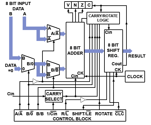
Connecting Digital Circuits Together.
Digital Electronics Modules 2 to 5 have described how basic logic gates may be combined, not only to perform standard logic functions, but to build circuits that can perform complex logic tasks. Both small scale integrated (SSI) and medium scale integrated (MSI) chips are available in many forms, that can be directly connected together to make very complex circuits. It is this inter-connectivity that makes digital electronics so powerful and so versatile.
The standard circuits described in modules 2 to 5, both combinational and sequential, can be used to perform arithmetic operations such as addition, subtraction and counting, as well as logical operations such as combining data sources (multiplexing) and shifting bits left or right within a binary word.
As explained in Module 1, binary arithmetic is normally carried out electronically by using twos complement notation. The most common and versatile method of carrying out such operations is in an Arithmetic and Logic Unit (ALU), a circuit that forms the heart of any calculating or computing system.
The Arithmetic and Logic Unit
A simplified ALU is illustrated in Fig 5.8.1, which uses an arrangement of both combinational and sequential circuits from those described in modules 2 to 5. Their purpose is to perform the basic (though still complex) binary arithmetic described in Module 1.
Data passing through the ALU circuit does so on a system of buses, shown by the broad arrows in Fig. 5.8.1. These buses consist of groups of wires (usually as 8 parallel bits in simple systems) each carrying a single byte of binary data. In this system, data word A is the primary data source, and data word B is the secondary data source that may be added to, or subtracted from word A.
The ALU can also perform other operations. It can increment, add 1 to word A, or decrement, subtract 1 from it. By complementing (inverting) the logic value of individual bits of the data word A and adding 1 to the result, it is possible to use twos complement arithmetic to perform subtractions.
The shift register at the ALU output can also perform a ‘logical shift-left’ on word A by shifting the 8 bits consecutively into the carry bit, alternatively the shift register can create a rotating pattern of bits, rotating left, and using the carry bit as a ninth bit in the sequence, or rotate the 8 bits right ignoring the carry bit. Any of these functions can be selected by the control block, using various combinations of the eight control lines shown in Fig. 5.8.1.
Putting the correct pattern of 1s and 0s (the control word) on the control lines will cause the ALU to perform the required arithmetic or logical operation on the data being input at A and B. With a control word of 8-bits, this could potentially allow up to 256 different combinations, or control words, which would be more than ample, even for very complex microprocessors or micro controllers. However this basic ALU needs only eight control words to control the different operations available.
To see the ALU operate as described below, you can download our free, fully interactive Logisim ALU circuit (assuming you have the free Logisim Digital Simulator installed on your desktop or laptop computer), see our extra Logisim page for details.

Fig. 5.8.2 Basic Arithmetic and Logic Unit - Logisim Simulation
The Component Parts
Any of the component parts of the Logisim design can be examined in detail by double clicking on the component (in simulation mode). To return to the main document, click ‘main’ in the component menu at the left of the screen.
Note: In this section the tilde character ~ is used where necessary to indicate NOT (e.g. ~LE = LE) to match the usage in the Logisim simulations.
")
Fig. 5.8.4 MUX 2

Fig. 5.8.3 MUX 1 and MUX 3
Multiplexers
MUX 1 and MUX 3 are identical 8 bit multiplexers that select either the input data word A (MUX 1) or data word B (MUX 3) or their internally generated complement, as shown in Fig. 5.8.3.
MUX 2 is a similar design but selects either the data word B or the zero value 00HEX , as shown in Fig. 5.8.4.

Fig. 5.8.5 The ALU Adder Component
8-Bit Adder
The adder component is an 8-bit ripple carry adder; real ALUs would normally feature a ‘carry-look-ahead’ adder, allowing for high-speed operation. However for this example the much simpler ripple carry adder is adequate, as the operation is totally manual.
The adder component is illustrated in Fig. 5.8.5 and consists of eight full-adder circuits with additional logic consisting of an XOR gate to detect overflow errors, and an 8-input NOR gate to detect a zero result.
Negative results are indicated by sampling the most significant bit of the ‘sum’ output, and a ‘carry’ is indicated by sampling the carry output of the most significant full adder.
Four D type flip-flops are used as ‘flag’ outputs to indicate the current state of the ALU after each operation.

Fig. 5.8.6 The ALU Shift Register Component
The Shift Register
This component uses two 4-bit shift registers (from Module 5.7) connected in cascade as shown in Fig. 5.8.6. Inputs are provided for clock pulses, (CK), a right/left shift control (R/~L) and an input to control whether the shift register is in shift, or load-enable modes (SHIFT/~LE).
If ~LE is chosen temporarily during shift operations, the shift register can be reloaded from the data placed on the 8-bit ‘Data A’ and ‘carry-in’ (CIN) inputs. This action is synchronised to the CK pulse by the external NAND and NOT gates connecting the SHIFT/~LE input to the two ~LOAD inputs of the 4-bit shift registers.
An additional JK flip-flop (mimicking a D type flip-flop) is placed between the ‘serial-right’ output of the shift register and COUT to allow the ‘clear carry’ input (~CLC) to clear the carry flag.

Fig.5.8.7 ALU Carry Logic
Carry Logic and Rotate Select
The carry logic circuit shown in Fig. 5.8.7 prevents the carry flag being set in rotate right mode, as bits rotate from bit 0 and re-enter the shift register at bit 7, therefore allowing correct carry flag operation in both left and right rotate modes.
When the ROTATE input is at logic 1, the Rotate Select circuit in Fig 5.8.7 allows COUT from the shift register to be fed back to the shift register CIN input for continuous bit rotation.
ALU Operation
Addition
To perform an addition, input data B is added to A. This is achieved by putting logic 1 on the control inputs of multiplexers 1, 2 and 3. This causes data A and B to be applied to the adder inputs. Also, to allow any carry bit from the CIN input to be included in the addition, the 1 bit carry multiplexer must have logic 0 on its control input. The shift register is only used as a PIPO register in addition mode, so its input lines R/~L and ROTATE must be at logic 0. SHIFT/~LE must also be at logic 0 to enable parallel loading of the shift register, which will hold the result of the addition (A plus B) after the application of a single CK pulse.
The Status Flags
The Flag flip-flops are special outputs from the adder circuit. They consist of four separate D type flip-flops, each of which can be set to 1 or cleared to 0. They are set or cleared by the result in the adder. They signal, or ‘flag’ to the user, that a particular event has occurred.
The Carry flag (C)
The carry flag will be set if the result of any arithmetic or logic event causes a logic 1 to be carried over from bit 7 into the ‘carry bit’, (which is the carry flag). The carry flag can be cleared at any time by making the ‘clear carry’ input (~CLC) logic 0.
The Overflow flag (V)
When carrying out twos complement arithmetic, errors can occur if large numbers are involved. For example if two positive numbers less than 12710 are added and produce a negative result (any value greater than 12710). This would cause the sign of the result (indicated by bit 7) to be wrong. The overflow flag gives an indication that an error has occurred by being set to 1 to indicate an ‘overflow error’. An error is sensed and the overflow flag is set when either of two conditions occurs.
There is a carry of logic 1 from bit 6 to bit 7 of the result, but the carry flip-flop is not at logic 1.
There is no carry from bit 6 to bit 7 of the result, but the carry flip-flop is at logic 1.
By using the carry-out from bit 6 and the carry-out from bit 7 of the result as inputs to an XOR gate, the output of the gate will be set to logic 1 for either of the above error conditions, signalling an overflow error at the overflow (V) flag.
The Zero flag (Z)
This flip-flop is set when every bit of the result is zero.
The Negative flag (N)
A negative result, i.e. bit 7 = 1 sets this flip-flop to logic 1.
The Flag Register
The status flags are individual bits of a register called the Flag Register, and are operative not only when the ALU is in addition mode, but also in all other arithmetic modes, the C flag is also operative in shift and rotate left modes. In microprocessors the flag register not only indicates ALU results, but can also be used in decision-making. For example the ALU can be used to compare (by subtracting) two values and take various actions depending on the state of particular flags; e.g. after comparing two values, A and B, an action may be taken if A = B, indicated by the zero flag being set to 1, otherwise (if the zero flag is set to 0) take no action.
Subtraction.
Subtraction is performed using twos complement arithmetic. That is, to subtract B from A, input B is complemented and 1 added to the complemented value to form the twos complement. Then the twos complement of B is added to A in the adder to find the result. To achieve this action with data A and data B present at the inputs, logic 1 is applied to the control inputs of MUX 1 and MUX 2. MUX 3 has logic 0 applied to its control input to complement data B, while the CARRY MUX has a logic 1 applied to its control line so that the carry-in (CIN) to the adder is forced to logic 1. This adds 1 to the result so that the twos complement of data B is added to data A. The result at the adder output is a twos complement number representing A - B. The flags are again set by the result as in the addition operation.
Counting with the ALU
Although the ALU does not include a binary counter circuit, it can also be used to count, by INCREMENTING or DECREMENTING, i.e. to add 1 to data A (incrementing), or subtract 1 from data A (decrementing). To count using this method would normally be carried out using (machine code or assembly language)software. A typical use could be to initiate a time delay by loading the ALU with some number, and then execute a looping routine to count down to zero by repeatedly decrementing data A. The zero result would be detected from the zero flag being set. However this would not be a common method, as the ALU (and therefore the CPU) would be occupied during the delay, and therefore not usable for other purposes. Most computer systems would also have dedicated counters for implementing similar time delays.
Incrementing.
Data A can be incremented if logic 1 is applied to the control inputs of MUX 1 and MUX 3. This will add B to A, with data B made zero by applying logic 0 to the control input of MUX 2. The 1 that must be added to data A is supplied by making the control input of the CARRY SELECT block logic 1, causing the carry input to the adder to be logic 1. The result at the adder output is therefore A + 1, again the flags are set by the result.
Decrementing.
To decrement data A, 1 must be subtracted from A. Because the ALU uses twos complement arithmetic, the twos complement of 1 added to A will in effect subtract 1 from A.
The twos complement of 1 is minus 1, which in 8-bit twos complement notation is 111111112. Therefore to subtract 1 from data A, data B must equal minus 1 (all bits = 1). To do this, and to make sure that the correct result is not changed by any data appearing on the data B input, logic 0 is applied to the control input of MUX 2 to make sure all data B bits = 0.
Logic 0 is also applied to the control input of MUX 3. This inverts data B, (which is 000000002) to give 111111112 at the adder input.
MUX 1 must have logic 1 on its control line, to apply data A to the other adder input. The adder’s carry input is set to 1 by applying logic 0 to the control line of the CARRY MUX. This ensures that, provided there is no carry-in on the CIN input, the correct result at the adder output will be A − 1.
Negation
Negation is simply the inverse of a value; therefore any value and its inverse will add to produce zero. In binary arithmetic the additive inverse of a value is its twos complement. The ALU can be used to negate (find the twos complement of) data A by complementing data A and then adding 1. This involves a similar process to decrementing, except that data B is treated differently, as follows:
The control input of MUX 1 is set to logic 0, which complements data A, also data B is made zero by putting logic 0 on MUX 2 control, and logic 1 on MUX 3. The Carry Select control input is set at logic 1, to add 1 to data A in the adder.
The shift register is used as a simple PIPO register by applying logic 0 to the three shift controls and logic 1 to the ~CLC input to make sure the carry is not cleared. This gives a final result of A+1, which is the twos complement of A.
The Shift Operations
Shift operations are controlled by the four lower order control lines, R/~L controls the direction of shift or rotation, SHIFT/~LE has the dual purpose of enabling the shift operations if logic 1 is applied, or acting as a LOAD ENABLE when at logic 0, allowing the shift register to be loaded or reloaded with appropriate data. Each action of the shift register (shift, rotate or load) is actuated by a single CK pulse. Also note that the shift register in this design does not affect the V, N or Z flags.
Shift Left (with Carry)
In this mode (with control word 10100101) input data B is kept at zero and, after the shift register is loaded by temporarily making SHIFT/~LE logic 0 to move data from input A into the shift register, shift is enabled by returning SHIFT/~LE to logic 1, and both ROTATE and ~CLC are disabled. The data in the shift register will now shift one bit to the left with each CK pulse applied. This appears to multiply the value of the data by two for each shift left, but it is a very limited multiplication operation, because the result is reduced each time the left most bit is lost as it passes through the carry bit. This action is therefore considered a logical, rather than an arithmetic shift.
Rotate Left (with Carry)
If rotate is activated by applying logic 1 to the ROTATE control input with SHIFT/~LE and ~CLC also at logic 1, the data being shifted left from bit 7 and through the carry flag, is returned via the CIN input of the shift register to re-enter at bit 0 by the action of the ROTATE MODE SELECT data selector.
Rotate Right
When data in the shift register is rotated right, it leaves the register via bit 0 and is returned directly to bit 7 via an internal link, without passing through the carry flag.
There are a number of other operations, such as performing 8 bit logic functions, commonly found on microprocessors that this ALU is not designed to do. The purpose of this design is to illustrate how the circuits described in Digital Electronics Modules 1 to 5 are really just part of a bigger picture, they can be inter-connected in many ways to make many different circuits.
Sequential Logic Quiz
Try our quiz, based on the information you can find in Digital Electronics Module 5 - Sequential Logic. Submit your answers and see how many you get right. If you get any answers wrong. Just follow the hints to find the right answer and learn more about sequential logic circuits as you go.
1.
Which of the listed flip-flops is also known as a programmable flip-flop?Power Supply Basics
Parts of a Power Supply
Ideally, a DC Power Supply Unit (commonly called a PSU) deriving power from the AC mains (line) supply performs a number of tasks:
- 1. It changes (in most cases reduces) the level of supply to a value suitable for driving the load circuit.
- 2. It produces a DC supply from the mains (or line) supply AC sine wave.
- 3. It prevents any AC from appearing at the supply output.
- 4. It will ensure that the output voltage is kept at a constant level, independent of changes in:
- a. The AC supply voltage at the supply input.
- b. The Load current drawn from the supply output.
- c. Temperature.
To do these things the basic PSU has four main stages, illustrated in Fig. 1.0.1

Fig. 1.0.1 Power Supply Block Diagram
Power supplies in recent times have greatly improved in reliability but, because they have to handle considerably higher voltages and currents than any or most of the circuitry they supply, they are often the most susceptible to failure of any part of an electronic system.
Modern power supplies have also increased greatly in their complexity, and can supply very stable output voltages controlled by feedback systems. Many power supply circuits also contain automatic safety circuits to prevent dangerous over voltage or over current situations.
The power modules on Learnabout-electronics therefore introduce many of the techniques used in modern power supplies, the study of which is essential to an understanding of electronic systems.
Warning

If you are considering building or repairing a power supply, especially one that is powered from mains (line) voltages the power supply modules on this site will help you understand how many commonly encountered circuits work. However you must realise that the voltages and currents present in many power supplies are, at best dangerous, and can be present even when the power supply is switched off! At worst, the high voltages present in power supplies can, and from time to time do KILL.
The Transformer


Fig. 1.1.1 Typical Input Transformer
In a basic power supply the input power transformer has its primary winding connected to the mains (line) supply. A secondary winding, electro-magnetically coupled but electrically isolated from the primary is used to obtain an AC voltage of suitable amplitude, and after further processing by the PSU, to drive the electronics circuit it is to supply.
The transformer stage must be able to supply the current needed. If too small a transformer is used, it is likely that the power supply's ability to maintain full output voltage at full output current will be impaired. With too small a transformer, the losses will increase dramatically as full load is placed on the transformer.
As the transformer is likely to be the most costly item in the power supply unit, careful consideration must be given to balancing cost with likely current requirement. There may also be a need for safety devices such as thermal fuses to disconnect the transformer if overheating occurs, and electrical isolation between primary and secondary windings, for electrical safety.
The Rectifier Stage

Three types of silicon diode rectifier circuit may be used, each having a different action in the way that the AC input is converted to DC. These differences are illustrated in Figs. 1.1.2 to 1.1.6
Half Wave Rectification

Fig. 1.1.2 Half Wave Rectification

Fig. 1.1.3 Full Wave Rectification

Fig. 1.1.4 The Bridge Rectifier

Fig. 1.1.5 Current Flow on the Positive Half Cycle

Fig. 1.1.6 Current Flow on the Negative Half Cycle
A single silicon rectifier diode may be used to obtain a DC voltage from the AC input as shown in Fig 1.1.2. This system is cheap but is only suitable for fairly non-demanding uses. The DC voltage produced by the single diode is less than with the other systems, limiting the efficiency of the power supply, and the amount of AC ripple left on the DC supply is generally greater.
The half wave rectifier conducts on only half of each cycle of the AC input wave, effectively blocking the other half cycle, leaving the output wave shown in Fig. 1.1.2. As the average DC value of one half cycle of a sine wave is 0.637 of the peak value, the average DC value of the whole cycle after half wave rectification will be 0.637 divided by 2, because the average value of every alternate half cycle where the diode does not conduct, will of course be zero. This gives an output of:
Vpk x 0.318
This figure is approximate, as the amplitude of the half cycles for which the diode conducts will also be reduced by about 0.6V due to the forward voltage drop (or Forward Junction Potential) of the silicon rectifier diode. This additional voltage drop may be insignificant when large voltages are rectified, but in low voltage power supplies where the AC from the secondary winding of the mains transformer may be only a few volts, this 0.6V drop across the diode junction may have to be compensated for, by having a slightly higher transformer secondary voltage.
Half wave rectification is not very efficient at producing DC from a 50Hz or 60Hz AC input. In addition the gaps between the 50 or 60Hz diode output pulses make it more difficult to remove the AC ripple remaining after rectification.
Full Wave Rectification
If a transformer with a centre tapped secondary winding is used, more efficient full wave rectification can be used. The centre-tapped secondary produces two anti-phase outputs, as shown in Fig 1.1.3.
If each of these outputs is ‘half wave rectified’ by one of the two diodes, with each diode conducting on alternate half cycles, two pulses of current occur at every cycle, instead of once per cycle in half wave rectification. The output frequency of the full wave rectifier is therefore twice the input frequency. This effectively provides twice the output voltage of the half wave circuit, Vpk x 0.637 instead of Vpk x 0.318 as the ‘missing’ half cycle is now rectified, reducing the power wasted in the half wave circuit. The higher output frequency also makes the smoothing of any remaining AC ripple easier.
Although this full wave design is more efficient than the half wave, it requires a centre tapped (and therefore more expensive) transformer.
The Bridge Rectifier
The full wave bridge rectifier uses four diodes arranged in a bridge circuit as shown in Fig. 1.1.4 to give full wave rectification without the need for a centre-tapped transformer. An additional advantage is that, as two diodes (effectively in series) are conducting at any one time, the diodes need only half the reverse breakdown voltage i.e the 'Maximum Working Peak Reverse Voltage (VRWM)' capability of diodes used for half and conventional full wave rectification. The bridge rectifier can be built from separate diodes or a combined bridge rectifier can be used.
The current paths on positive and negative half cycles of the input wave are shown in Fig. 1.1.5 and Fig. 1.1.6. It can be seen that on each half cycle, opposite pairs of diodes conduct, but the current through the load remains in the same polarity for both half cycles.
Filter Components
A typical power supply filter circuit can be best understood by dividing the circuit into two parts, the reservoir capacitor and the low pass filter. Each of these parts contributes to removing the remaining AC pulses, but in different ways.
The Reservoir Capacitor

Fig. 1.2.1 The Reservoir Capacitor
Fig. 1.2.1 shows an electrolytic capacitor used as a reservoir capacitor, so called because it acts as a temporary storage for the power supply output current. The rectifier diode supplies current to charge a reservoir capacitor on each cycle of the input wave. The reservoir capacitor is a large electrolytic, usually of several hundred or even a thousand or more microfarads, especially in mains frequency PSUs. This very large value of capacitance is required because the reservoir capacitor, when charged, must provide enough DC to maintain a steady PSU output in the absence of an input current; i.e. during the gaps between the positive half cycles when the rectifier is not conducting.
The action of the reservoir capacitor on a half wave rectified sine wave is shown in Fig. 1.2.2. During each cycle, the rectifier anode AC voltage increases towards Vpk. At some point close to Vpk the anode voltage exceeds the cathode voltage, the rectifier conducts and a pulse of current flows, charging the reservoir capacitor to the value of Vpk.

Fig. 1.2.2 Reservoir Capacitor Action
Once the input wave passes Vpk the rectifier anode falls below the capacitor voltage, the rectifier becomes reverse biased and conduction stops. The load circuit is now supplied by the reservoir capacitor alone (hence the need for a large capacitor).
Of course, even though the reservoir capacitor has large value, it discharges as it supplies the load, and its voltage falls, but not by very much. At some point during the next cycle of the mains input, the rectifier input voltage rises above the voltage on the partly discharged capacitor and the reservoir is re-charged to the peak value Vpk again.
AC Ripple
The amount by which the reservoir capacitor discharges on each half cycle is determined by the current drawn by the load. The higher the load current, the more the discharge, but provided that the current drawn is not excessive, the amount of the AC present in the output is much reduced. Typically the peak-to-peak amplitude of the remaining AC (called ripple as the AC waves are now much reduced) would be no more than 10% of the DC output voltage.
The DC output of the rectifier, without the reservoir capacitor, is either 0.637 Vpk for full wave rectifiers, or 0.317 Vpk for half wave. Adding the capacitor increases the DC level of the output wave to nearly the peak value of the input wave, as can be seen from Fig. 1.1.9.
To obtain the least AC ripple and the highest DC level it would seem sensible to use the largest reservoir capacitor possible. There is a snag however. The capacitor supplies the load current for most of the time (when the diode is not conducting). This current partly discharges the capacitor, so all of the energy used by the load during most of the cycle must be made up in the very short remaining time during which the diode conducts in each cycle.
The formula relating charge, time and current states that:
Q = It
The charge (Q) on a capacitor depends on the amount of current (I) flowing for a time (t).
Therefore the shorter the charging time, the larger current the diode must supply to charge it. If the capacitor is very large, its voltage will hardly fall at all between charging pulses; this will produce a very small amount of ripple, but require very short pulses of much higher current to charge the reservoir capacitor. Both the input transformer and the rectifier diodes must be capable of supplying this current. This means using a higher current rating for the diodes and the transformer than would be necessary with a smaller reservoir capacitor.
There is an advantage therefore in reducing the value of the reservoir capacitor, thereby allowing an increase in the ripple present, but this can be effectively removed by using a low pass filter and regulator stages between the reservoir capacitor and the load.
This effect of increasing reservoir size on diode and transformer current should be born in mind during any servicing operations; replacing the reservoir capacitor with a larger value than in the original design "to reduce mains hum" may seem like a good idea, but could risk damaging the rectifier diode and/or the transformer.
With full wave rectification the performance of the reservoir capacitor in removing AC ripple is significantly better than with half wave, for the same size of reservoir capacitor, the ripple is about half the amplitude of that in half wave supplies, because in full wave circuits, discharge periods are shorter with the reservoir capacitor being recharged at twice the frequency of the half wave design.
Low Pass Filters
Although a useable power supply can be made using only a reservoir capacitor to remove AC ripple, it is usually necessary to also include a low pass filter and/or a regulator stage after the reservoir capacitor to remove any remaining AC ripple and improve the stabilisation of the DC output voltage under variable load conditions.

Fig. 1.2.3 LC Filter

Fig. 1.2.4 RC Filter
Either LC or RC low pass filters can be used to remove the ripple remaining after the reservoir capacitor. The LC filter shown in Fig. 1.2.3 is more efficient and gives better results than the RC filter shown in Fig. 1.2.4 but for basic power supplies, LC designs are less popular than RC, as the inductors needed for the filter to work efficiently at 50 to 120Hz need to be large and expensive laminated or toroidal core types. However modern designs using switch mode supplies, where any AC ripple is at much higher frequencies, much smaller ferrite core inductors can be used.
The low pass filter passes low frequency, in this case DC (0Hz) and blocks higher frequencies, whether 50Hz or 120Hz in basic circuits or tens of kHz in switch mode designs.
The reactance(XC) of the capacitor in the either of the filters is very low compared with the resistance of resistor R or the reactance of the choke XL at the ripple frequency. In RC designs the resistance of R must be a fairly low value as the entire load current, maybe several amperes, must pass through it, generating a considerable amount of heat. A typical value would therefore be 50 ohms or less, and even at this value, a large wire wound resistor would normally need to be used. This limits the efficiency of the filter as the ratio between the resistance of R and the capacitor reactance will not be greater than about 25:1. This then would be the typical reduction ratio of the ripple amplitude. By including the low pass filter some voltage is lost across the resistor, but this disadvantage is offset by the better ripple performance than by using the reservoir capacitor alone.
The LC filter performs much better than the RC filter because it is possible to make the ratio between XC and XLmuch bigger than the ratio between XC and R. Typically the ratio in a LC filter could be 1:4000 giving much better ripple rejection than the RC filter. Also, since the DC resistance of the inductor in the LC filter is much less than the resistance of R in the RC filter, the problem of heat being generated by the large DC current is very much reduced in LC filters.
With a combined reservoir capacitor and low pass filter it is possible to remove 95% or more of the AC ripple and obtain an output voltage of about the peak voltage of the input wave. A simple power supply consisting of only transformer, rectifier, reservoir and low pass filter however, does have some drawbacks.

Fig. 1.2.5 DC Adaptor
The output voltage of the PSU tends to fall as more current is drawn from the output. This is due to:
a. The reservoir capacitor being discharged more on each cycle.
b. Greater voltage drop across the resistor or choke in the low pass filter as current increases.
These problems can be largely overcome by including a regulator stage at the power supply output as described in Power Supplies Module 2.
The basic power supply circuits described here in Module 1 however, are commonly used in the common ‘wall wart’ type DC adaptors supplied with many electronics products. The most common versions comprise a transformer, bridge rectifier and sometimes a reservoir capacitor. Additional filtering and regulation/stabilisation being usually performed in the circuit supplied by the adaptor.
Power Supply Basics Quiz
Try this quiz, based on the information you can find in Power Supplies Module 1. Submit your answers and see how many you get right. If you get any answers wrong, just follow the hints to find the right answer and learn about Power Supplies as you go.
1.
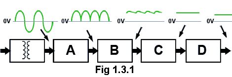
Switched Mode Power Supplies
Introduction
Switched Mode Power Supplies, (often abbreviated to SMPS) are consider . The main advantage of this added complexity is that switched mode operation gives regulated DC supplies that can deliver more power for a given size, cost and weight of power unit.
Switched Mode Designs
A number of different design types are used. Where the input is the AC mains (line) supply the AC is rectified and smoothed by a reservoir capacitor before being processed by what is in effect a DC to DC converter, to produce a regulated DC output at the required level. Hence a SMPS can be used as an AC to DC converter, for use in many mains powered circuits, or DC to DC, either stepping the DC voltage up or down as required, in battery powered systems.
Switched Mode Block Diagram

Fig. 3.0.1 Typical SMPS Block Diagram
Fig. 3.0.1 shows a block diagram example of a typical SMPS with an AC Mains (line) input and a regulated DC output. The output rectification and filter are isolated from the High Frequency switching section by a high frequency transformer, and voltage control feedback is via an opto isolator. The control circuit block is typical of specialist ICs containing the high frequency oscillator, pulse width modulation, voltage and current control and output shut down sections.
Whatever the purpose of a SMPS, a common feature (after conversion of AC to DC if required) is the use of a high frequency square wave to drive an electronic power switching circuit. This circuit is used to convert the DC supply into high frequency, high current AC, which by various means, depending on the design of the circuit, is reconverted into a regulated DC output. The reason for this double conversion process is that, by changing the DC or mains frequency AC to a high frequency AC, the components, such as transformers, inductors and capacitors, needed for conversion back to a regulated DC supply, can be much smaller and cheaper than those needed to do the same job at mains (line) frequency.
The high frequency AC produced during the conversion process is a square wave, which provides a means of controlling the output voltage by means of pulse width modulation. This allows the regulation of the output to be much more efficient than is possible in linear regulated supplies.
The combination of a square wave oscillator and switch used in switched mode supplies can also be used to convert DC to AC. In this way the switched mode technique also be used as an ‘inverter’ to create an AC supply at mains potential from DC supplies such as batteries, solar panels etc.
Voltage Regulation
In most switched mode supplies, regulation of both line (input voltage) and load (output voltage) is normally provided. This is achieved by altering the mark to space ratio of the oscillator waveform before applying it to the switches. Control of the mark to space ratio is achieved by comparing voltage feedback from the output of the supply with a stable reference voltage. By using this feedback to control the mark to space ratio of the oscillator, the duty cycle and therefore the average DC output of the circuit can be controlled. In this way, protection from both over voltage and over current may be provided.
Where it is important to maintain electrical isolation from the mains supply, this is provided by using a transformer, either at the AC input where it may also be used to alter the AC voltage prior to rectification, or between the control section of the power supply and the output section where, as well as providing isolation, a transformer with multiple secondary windings can produce several different voltage outputs.
To provide a well regulated output, a sample of the DC output voltage is normally fed back to the control circuitry and compared with a stable reference voltage. Any error produced is used to control the output voltage. To maintain electrical isolation between input and output, feedback will usually be via a device such as an opto-isolator.
HF Switching
Using high frequency for the switching drive gives several advantages:
• The transformer will be of a HF type, which is much smaller than a standard mains transformer.
• The ripple frequency will be much higher (e.g. 100kHz) than in a linear supply, and so it needs a smaller value of smoothing capacitor.
• Also using a square wave to drive the switching transistors (switched mode operation) ensures that they dissipate much less power than a conventional series regulator transistor. Again this means that, for a given amount of power output, smaller and cheaper transistors can be used, than in similarly rated linear power supplies.
• The use of smaller transformers and smoothing capacitors makes switched mode power supplies lighter and less bulky. The added cost of the complex control circuitry is also offset by the smaller, and therefore cheaper transformers and smoothing capacitors, making some switched mode designs less expensive than equivalent linear supplies.
Although linear supplies can provide better regulation and better ripple rejection at low power levels than switched mode supplies, the above advantages make the SMPS the most common choice for power supply units in any equipment where a stabilised supply is needed to deliver medium to large amounts of power.
A disadvantage of using such a high frequency square wave in a powerful circuit such as a SMPS is that many powerful high frequency harmonics are created, so that without very effective RF screening and filtering, there is a danger of the SMPS creating RF interference.
Push-Pull Switched Mode Power Supplies
Fig. 3.4.1 shows a block diagram of a switched mode power supply designed around a UC3524 Advanced Regulating Pulse Width Modulator by Texas Instruments.
The circuit is a DC to DC converter using a DC input voltage of 15V to 30V and produces a regulated 5V output at a current up to about 250mA. The circuit uses push pull power switching driving a high frequency transformer, which fully isolates the output circuit from the input. The output is short circuit protected, and the output voltage can be manually adjusted. Maximum current can be also manually set using adjustable current limiting.
Primary Circuit.
A 100kHz oscillator within IC1 (UC3524) generates pulses, which are processed by the pulse width modulator (within IC1)used to drive the power switching transistors. The width of the processed drive pulses controls the length of time for which the power switching transistors conduct, and therefore the amount of power delivered to the transformer.
The pulse width and therefore the output voltage is controlled by the error amplifier in IC1. This measures the difference between a sample of the output voltage, fedback via the opto-isolator, and a reference voltage set by Vr1. When these two voltages are equal, the circuit output voltage is correct. If there is a difference, the width of the pulses produced by the pulse width modulator is increased or decreased to correct the error.
Over current protection is provided to ensure that the supply is shut down in the event of too high a current demand at the output. The output terminals can even be shorted together without damaging the supply.
Each pulse of current in the power switching transistors produces a voltage pulse across the sensing resistor R12. The amplitude of these pulses is proportional to the current being delivered to the transformer by the switching circuit. If the peak value of any of these pulses exceeds the DC voltage set by Vr2 (Current limit) then the output from IC2 will cause pulse width modulator input to reduce the width of the pulse being produced by the modulator at that time, momentarily reducing the output voltage. If the over current condition disappears, the output voltage will be restored to its normal level, but if the load current remains high, the current limiter will continue to reduce the pulse width, dependent on the amount of over current, even down to zero in the case of a short circuit output.
The Secondary Circuit
The push pull switching transistors create an AC waveform across the transformer primary winding, and the secondary winding feeds a conventional full wave rectifier and LC low pass filter to supply the load with a stable 5V at the output terminals. Negative feedback to the voltage regulating circuit in IC1 is via the opto-isolator (IC3). The higher the output voltage, the brighter the glow from an LED sealed within the secondary side, and the larger the DC output voltage derived from pin 4 of IC3 in the primary side of the device. This voltage is used as a sample at the inverting input of the error amplifier in IC1 where it is compared with a voltage from the ‘set voltage’ control VR1, to control the pulse width modulator.
Circuit Description
The full schematic diagram for the circuit is shown in Fig. 3.4.2.

Fig. 3.4.2 Circuit diagram of a push-pull SMPS using the Texas Instruments UC3524 I.C.

Fig. 3.4.3 The UC3524N (part detail)
The oscillator within IC1 produces narrow 100kHz (approx) pulses that are used as clock pulses for the Switch Logic within IC1. The timing components for the oscillator are R3 and C2. The ramp waveform produced as C2 charges is also used as an input to the inverting input of the comparator in IC1.
The pulse width modulator comprises the comparator within IC1 and the switching logic, which consists of a bistable and two three input NOR gates. The outputs of this block supply variable width pulses to the two transistors Qa and Qb.
The error amplifier compares a stable reference voltage on pin 1 (set by Vr1 supplied from an internally regulated 5V from pin 16) with a sample of the load voltage developed across the opto-isolator emitter resistor, R11. The resulting error voltage is used as the non-inverting input to the PWM comparator.
The facilities of the UC3524 that are used in this circuit are shown in more detail in Fig. 3.4.3 (Note: Some unused facilities of the UC3524 have been omitted for clarity, for more information see the Texas Instruments UC3524 data sheet).
Pulse Width Modulator

Fig. 3.4.4 UC3524N and Transformer Primary Waveforms
The action of the pulse width modulator, described by the waveforms shown in Fig. 3.4 4 is as follows:
Clock pulses (CK) from the oscillator are fed to the Bi-stable (flip-flop), which produces a square wave with a 1:1 mark/space ratio and a frequency of 50kHz, (half that of the oscillator) at its Q output, and an inverted version of this wave at its Q output.
Output Q provides an input to NOR gate a, and output Q (the opposite of Q) provides an input to NOR gates b. The logic rule for a NOR gate is that its output will be high, only when all its three inputs are low. Notice that the Q and Q signals go low at the start of alternate clock pulse low states. The clock signal also provides an input to both NOR gates.
The third input to each of the NOR gates is provided by the comparator output, which is a series of variable width low state pulses, produced by comparing the DC error voltage from the error amplifier in IC1 with the ramp produced by the oscillator timing capacitor C2.
As each NOR gate output goes high, only when all of its three input signals are low, alternate high state pulses, whose width depends on the value of the error voltage, are fed to the bases of the internal transistors Qa and Qb. The lower the value of the error voltage (due to a higher value of "sample" voltage at pin 1) the narrower the pulses produced. These narrower pulses, when used to turn on the power switching transistors TR3 and Tr4, will lead to a reduction in power in the transformer and a reduction in load voltage.
Power Switching Circuits

Fig. 3.4.5 Speeding up the Power Switch Turn Off
The internal drive transistors Qa and Qb each produces a series of pulses at its collector, and an a series of anti-phase pulses at its emitter. The emitter signals a and b drive the power switching transistors Tr3 and Tr4 respectively, and the collector signals drive the speed up circuits Tr1/Tr2.
The reason for including the speed up circuits is to overcome the delay that would normally happen because while the power switching transistors Tr3 andTr4 are conducting, their base/emitter junction (which naturally forms a small capacitor due to the depletion layer between the base and emitter layers in the transistor) is charged up, and must be discharged before the transistor will fully turn off.
The power transistor junctions are rapidly discharged by momentarily turning on Tr1 or Tr2 using a differentiated pulse generated from the rising edge of the waveform from the collector of Qa or Qb in IC1, which of course happens at exactly the same instant as Tr3 or Tr4 is turning off, as illustrated in Fig 3.4.5.
Because the transformer primary centre tap is connected to the main (+VIN) supply, it will always be at the supply potential. The collector voltages of Tr3 and Tr4 will also be at +VIN during the periods when both transistors are turned off.
During the ‘on’ pulse of Tr3, its collector will be at approximately 0V, and due to the centre tapping of the transformer primary winding the bottom half of the primary will be in anti-phase to the top half, so the collector of Tr4 will be positive at twice the value of +VIN for the period of the Tr3 ‘on’ pulse. This situation is reversed during the ‘on’ pulse of Tr4. This action produces a stepped type of waveform with an amplitude of +VIN x 2 across the transformer primary as shown in Fig 3.4.4.
The Secondary Circuit
The resulting secondary voltage is rectified by D1 and D2, and smoothed by the low pass filter L1/C10 before being supplied to the load. A sample of the load voltage is fed back to the LED within opto-isolator IC3 via the LED current limiting resistor R13.

Fig. 3.4.6 Typical High Frequency
Multi-Secondary Transformer
Because of the push pull design used by this circuit, it is a simple matter to arrange for such a circuit to have multiple outputs. Different (higher or lower) voltages can be obtained by using a transformer similar to the one illustrated in Fig. 3.4.6, which has multiple secondary windings with appropriate turns ratios.
The total current supplied to the multiple outputs however, must not exceed the maximum current rating of the SMPS. Each supply line will have its own rectifier and filter system, and may also include some extra point of load regulation. A voltage sample will normally be taken from only one of the outputs to provide feedback to the pulse width modulator however, as controlling the power applied to the transformer primary will control all the voltage outputs.
Current limiting
Current limiting, which is capable of completely shutting down the circuit under extreme overload conditions is provided by the action of IC2 and the shut down transistor between pins 9 and 10 within IC1.
Pin 3 of IC2 is provided with a stable reference voltage derived from the shunt voltage regulator R7/ZD1 via the current limit control Vr2. The non-inverting input of IC2 is connected to a low resistance current sensing resistor R12 in the emitter lead common to both switching transistors Tr3/Tr4.
Every time either transistor conducts, the resulting large emitter current produces a voltage pulse across R12. The peak voltage of this pulse will be proportional to the emitter current flowing in Tr3/Tr4 and therefore, also to the output current.
If the peak voltage of any of these pulses applied to the non-inverting input of IC2 exceeds the stabilised DC voltage at the inverting input, a positive pulse will be produced at the output, and therefore at the base of Qc within IC1. This will cause the collector voltage of this transistor to fall, also reducing the error amplifier output that is controlling the pulse width modulator. This action has the effect of reducing the width of the pulse presently being produced, thus instantly reducing output voltage. If the current overload disappears, the pulse width modulator will return to normal operation. If not, subsequent pulses will be further reduced until the output voltage falls (if necessary) to zero.
The action of the current limit circuit is not absolutely instant however, due to the presence of C4 on the shut down compensation pin (9) of IC1. This capacitor tends to integrate the voltage changes on the collector of the shut down transistor so that very rapid (cycle by cycle) variations of the output voltage during current limiter action are avoided.
What is an Oscillator
An oscillator provides a source of repetitive A.C. signal across its output terminals without needing any input (except a D.C. supply). The signal generated by the oscillator is usually of constant amplitude.
The wave shape and amplitude are determined by the design of the oscillator circuit and choice of component values.
The frequency of the output wave may be fixed or variable, depending on the oscillator design.
Types of Oscillator
 Circuit Symbol")
Fig. 1.0.1 Oscillator
(AC Source)
Circuit Symbol
Oscillators may be classified by the type of signal they produce.
- SINE WAVE OSCILLATORS produce a sine wave output.
- RELAXATION OSCILLATORS and ASTABLE MULTIVIBRATORS produce Square waves and rectangular pulses.
- SWEEP OSCILLATORS produce sawtooth waves.
Sine wave oscillators can also be classified by frequency, or the type of frequency control they use. RF (radio frequency) oscillators working at frequencies above about 30 to 50kHz use LC (inductors and capacitors) or Crystals to control their frequency. These may also be classified as HF, VHF, and UHF oscillators, depending on their frequency.
LF (low frequency) oscillators are generally used for generating frequencies below about 30kHz and are usually RC oscillators, as they use resistors and capacitors to control their frequency.
Square wave oscillators such as relaxation and astable oscillators may be used at any frequency from less than 1Hz up to several GHz and are very often implemented in integrated circuit form.
Sine Wave Oscillators.

Fig. 1.0.2 Frequency Control Networks
These circuits ideally produce a pure sine wave output having a constant amplitude and stable frequency. The type of circuit used depends on a number of factors, including the frequency required. Designs based on LC resonant circuits or on crystal resonators are used for ultrasonic and radio frequency applications, but at audio and very low frequencies the physical size of the resonating components, L and C would be too big to be practical.
For this reason a combination of R and C is used to a control frequency. The circuit symbols used for these frequency control networks are shown in Fig. 1.0.2
LC oscillators

Inductors and capacitors are combined in a resonating circuit that produces a very good shape of sine wave and has quite good frequency stability. That is, the frequency does not alter very much for changes in the D.C. supply voltage or in ambient temperature, but it is relatively simple, by using variable inductors or capacitors, to make a variable frequency (tuneable) oscillator. LC oscillators are extensively used in generating and receiving RF signals where a variable frequency is required.
RC (or CR) oscillators

At low frequencies such as audio the values of L and C needed to produce a resonating circuit would be too large and bulky to be practical. Therefore resistors and capacitors are used in RC filter type combinations to generate sine waves at these frequencies, however it is more difficult to produce a pure sine wave shape using R and C. These low frequency sine wave oscillators are used in many audio applications and different designs are used having either a fixed or variable frequency.
Crystal oscillators

At radio frequencies and higher, whenever a fixed frequency with very high degree of frequency stability is needed, the component that determines the frequency of oscillation is usually a quartz crystal, which when subjected to an alternating voltage, vibrates at a very precise frequency. The frequency depends on the physical dimensions of the crystal, therefore once the crystal has been manufactured to specific dimensions, the frequency of oscillation is extremely accurate. Crystal oscillator designs can produce either sine wave or square wave signals, and as well as being used to generate very accurate frequency carrier waves in radio transmitters, they also form the basis of the very accurate timing elements in clocks, watches, and computer systems.
Relaxation oscillators

These oscillators work on a different principle to sine wave oscillators. They produce a square wave or pulsed output and generally use two amplifiers, and a frequency control network that simply produces a timing delay between two actions. The two amplifiers operate in switch mode, switching fully on or fully off alternately, and as the time, during which the transistors are actually switching, only lasts for a very small fraction of each cycle of the wave, the rest of the cycle they "relax" while the timing network produces the remainder of the wave. An alternative name for this type of oscillator is an "astable multivibrator", this name comes from the fact that they contain more than one oscillating element. There are basically two oscillators, i.e. ''vibrators'', each feeding part of its signal back to the other, and the output changes from a high to a low state and back again continually, i.e. it has no stable state, hence it is astable. Relaxation oscillators can be built using several different designs and can work at many different frequencies. Astables may typically be chosen for such tasks as producing high frequency digital signals. They are also used to produce the relatively low frequency on-off signals for flashing lights.
Sweep oscillators

A sweep waveform is another name for a saw-tooth wave. This has a linearly changing (e.g increasing) voltage for almost the whole of one cycle followed by a fast return to the wave’s original value. This wave shape is useful for changing (sweeping) the frequency of a voltage-controlled oscillator, which is an oscillator that can have its frequency varied over a set range by having a variable ‘sweep’ voltage applied to its control input. Sweep oscillators often consist of a ramp generator that is basically a capacitor charged by a constant value of current. Keeping the charging current constant whilst the charging voltage increases, causes the capacitor to charge in a linear fashion rather than its normal exponential curve. At a given point the capacitor is rapidly discharged to return the signal voltage to its original value. These two sections of a saw-tooth wave cycle are called the sweep and the fly-back.
Parts of an Oscillator
Most oscillators consist of three basic parts:
1. An amplifier. This will usually be a voltage amplifier and may be biased in class A, B or C.
2. A wave shaping network. This consists of passive components such as filter circuits that are responsible for the shape and frequency of the wave produced.
3. A POSITIVE feedback path. Part of the output signal is fed back to the amplifier input in such a way that the feed back signal is regenerated, re-amplified and fed back again to maintain a constant output signal.
Commonly an oscillator is constructed from an amplifier that has part of its output signal fed back to its input. This is done in such a way as to keep the amplifier producing a signal without the need for any external signal input as shown in Fig. 1.1.1. It can also be thought of as a way of converting a DC supply into an AC signal.
Positive feedback.
The feedback in the amplifier section of an oscillator must be POSITIVE FEEDBACK. This is the condition where a fraction of the amplifier's output signal is fed back to be in phase with the input, and by adding together the feedback and input signals, the amplitude of the input signal is increased. For example, a common emitter amplifier creates a phase change of 180° between its input and output, the positive feedback loop must therefore also produce a 180° phase change in the signal fed back from output to input for positive feedback to occur.
The result of a small amount of positive feedback in amplifiers is higher gain, though at the cost of increased noise and distortion. If the amount of positive feedback is large enough however, the result is oscillation, where the amplifier circuit produces its own signal.
Using Positive Feedback.
When an amplifier is operated without feedback it is operating in "open loop" mode. With feedback (either positive or negative) it is in "closed loop" mode. In ordinary amplifiers negative feedback is used to provide advantages in bandwidth, distortion and noise generation, and in these circuits the closed loop gain of the amplifier is much less than the open loop gain. However when positive feedback is used in an amplifier system the closed loop gain (with feedback) will be greater than the open loop gain, the amplifier gain is now increased by the feedback. Additional effects of positive feedback are reduced bandwidth, (but this does not matter in an oscillator producing a sine wave having a single freqency), and increased distortion. However even quite severe distortion in the amplifier is allowed in some sine wave oscillator designs, where it does not affect the shape of the output wave.
In oscillators using positive feedback it is important that amplitude of the oscillator output remains stable. Therefore the closed loop gain must be 1 (unity). In other words, the gain within the loop (provided by the amplifier) should exactly match the losses (caused by the feedback circuit) within the loop. In this way there will be no increase or decrease in the amplitude of the output signal, as illustrated in Fig. 1.1.2.
The conditions for oscillation.
Positive feedback must occur at a frequency where the voltage gain of the amplifier is equal to the losses (attenuation) occurring in the feedback path. For example if 1/30th of the output signal is fed back to be in phase with the input at a particular frequency, and the gain of the amplifier (without feedback) is 30 times or more, oscillation will take place.
The oscillations should take place at one particular frequency.
The amplitude of the oscillations should be constant.
There are many different oscillator designs in use, each design achieving the above criteria in different ways. Some designs are particularly suited to producing certain wave shapes, or work best within a certain band of frequencies. Whatever design is used however, the way of achieving a signal of constant frequency and constant amplitude is by using one or more of three basic methods
.
Method 1
Make sure that positive feedback occurs only at one frequency, the required frequency of oscillation. This may be achieved by ensuring that only signals of the required frequency are fed back, or by ensuring the feedback signal is in the correct phase at only one frequency.
Method 2
Make sure that sufficient amplification for oscillation can take place only at the required frequency, by using an amplifier that has an extremely narrow bandwidth, extending to the frequency of oscillation only.
Method 3
Use amplifiers in "switch mode" to switch the output between two set voltage levels, together with some form of time delay to control the time at which the amplifiers switch on or off, thus controlling the periodic time of the signal produced.

Fig. 1.1.2 The Need For Amplitude Stability
Methods 1 and 2 are used extensively in sine wave oscillators, while method 3 is useful in square wave generators, sometimes called aperiodic (untuned) oscillators. Oscillators using method 3 often use more than one amplifier and timing circuit, and so are called multivibrators (more than one oscillator).
Constant Amplitude
As shown in Fig. 1.1.1 oscillators must have an amplifier, a positive feedback loop and some method of controlling the frequency of oscillation. In RF sine wave oscillators the frequency may be controlled by an LC tuned circuit, but as well as controlling the frequency of oscillation, there must also be some means, such as negative feedback, of stabilising the amplitude of the signal produced.
Without this stabilisation the oscillations would either die away and stop (damped oscillation) or rapidly increase in amplitude until the amplifier produces severe distortion due to the transistors within the amplifier becoming "saturated" as shown in Fig. 1.1.2. To produce a constant amplitude output the gain of the amplifier is automatically controlled during oscillation.
CR Relaxation (Square Wave) Oscillators
Introduction
There are a number of oscillator designs that produce square waves at frequencies from less than 1Hz to several GHz. Square waves are used to control the timing of operations in digital systems, such as clock generators for microprocessors. They also have many uses in analogue circuits from simple lamp flashers to complex control systems as well as pulse width control systems for audio and radio applications.
These different circuits go under a variety of names, such as:
Astable oscillators
This name comes from the fact that these oscillators have no stable state; their output changes repeatedly from high to low and back to high.
Astable multivibrators
Some astables consist of more than one (e.g. two oscillating amplifiers).
Aperiodic Oscillators
Because they are untuned oscillators.
Clock Oscillators
In digital applications the main function of these oscillators is the production of square wave outputs, or pulse trains.
Square wave oscillators can also be used as the basis for sawtooth oscillators or sweep generators.
Properties of Square Waves

Fig. 4.0.1 Mark to Space Ratio
Square waves may be perfectly symmetrical with the height and width of both the mark and the space being equal, but this is not necessarily the case. Where the mark and the space are of equal width (time), the waveform is said to have a mark to space ratio of 1:1 but in the lower waveform in Fig. 1 the mark is twice the width of the space and so the mark to space ratio is 2:1.
The height (Voltage) of the mark does not need to be equivalent to its width, provided that the voltage and timing of the waveform is known.
Waveforms of a rectangular rather than square shape can also be considered square waves.
Where the time of the mark is much shorter than that of the space however, the waveform is more properly called a series of pulses or a pulse train as shown in Fig. 4.0.2.

Fig. 4.0.2 Pulse Train
With pulses the frequency of the wave is more usually referred to as the “Pulse repetition frequency” (p.r.f.), which refers to the number of pulses occurring in one second rather than the more usual Hz or cycles per second.
A square wave is a complex wave, meaning that unlike the sine wave, which has only a single sine component, it is made up of many sine wave components. It has a ‘fundamental’, a sine wave of the same amplitude and frequency as the square wave, plus, in a perfect square wave, an infinite number of odd harmonics. This means that to produce a perfect square wave, the oscillator and any circuits being fed by it, must have an infinitely wide bandwidth, with constant gain over the whole bandwidth. As this level of perfection is not practicable, it is to be expected that some distortion of the square wave will be present. Figs 4.0.3, 4 and 5 illustrate some commonly encountered distortions to square waves.
Rise and Fall Time

Fig. 4.0.3 Slow Rise & Fall Times
Fig. 4.0.3 shows a square wave in which the vertical edges are not vertical. The rise and fall in voltage should be instantaneous but here there is a distinct lengthening of the rise and fall times plus a certain amount of rounding of the waveform. This is typical of poor high frequency response in an oscillator or amplifier circuit, the higher frequency harmonics are reduced or missing, also causing a ‘rounding’ of the waveform. A similar effect, but without the rounding can be evident at higher frequencies in op amp astables due to slew rate limiting.
Ringing

Fig. 4.0.4 Ringing
Fig. 4.0.4 Illustrates ‘Ringing’ following the vertical transitions of the wave, this may be caused by the presence of stray inductance and capacitance in the circuit causing damped oscillations to begin at some high frequency, together with large high frequency gain.
Overshoot

Fig. 4.0.5 Overshoot
Fig. 4.0.5 illustrates ‘Overshoot’ where the rising and falling edges of the wave continue above and below the maximum amplitude of the wave. Overshoot is generally measured as a percentage of the total (normal) amplitude of the wave. It may be caused by the presence of stray inductance creating excessive high frequency gain.
Tidak ada komentar:
Posting Komentar