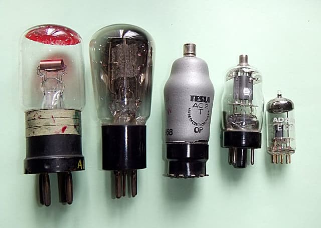
Vacuum Tubes: The World Before Transistors
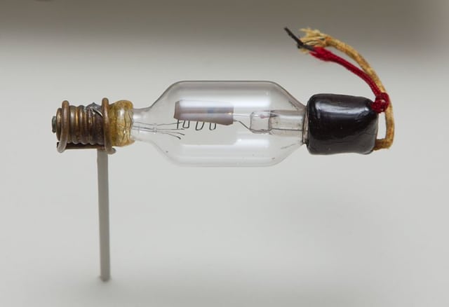
The original triode vacuum tube, the Audion, invented by Lee de Forest in 1906
In any modern-day electrical device—from alarm clocks to phones to computers to televisions—you’ll find a device called a transistor. In fact, you’ll find billions of them. Transistors are the atoms of modern-day computing, combining to create the logic gates that enable computation. The invention of the transistor in 1947 opened the door to the information age as we know it.
But computers existed before transistors did, albeit in a rather rudimentary form. These massive systems took up entire rooms, weighed thousands of pounds, and for all that, were nowhere near as powerful as the computers that we can fit in our pockets today.
Rather than being built out of transistors, these behemoth computers were made up of something called thermionic valves, aka vacuum tubes. These light bulb-looking devices are now more or less obsolete (with one or two notable exceptions), but in their heyday, they were critical to the design of many electronic systems, from radios to telephones to computers. In this article, we’ll take a look at how vacuum tubes work, why they went away, and why they didn’t go away entirely.
Thermionic EmissionThe basic working principle of a vacuum tube is a phenomenon called thermionic emission. It works like this: you heat up a metal, and the thermal energy knocks some electrons loose. In 1904, English physicist John Ambrose Fleming took advantage of this effect to create the first vacuum tube device, which he called an oscillation valve.
Fleming’s device consisted of two electrodes, a cathode and an anode, placed on either end of an encapsulated glass tube.When the cathode is heated, it gives off electrons via thermionic emission. Then, by applying a positive voltage to the anode (also called the plate), these electrons are attracted to the plate and can flow across the gap. By removing the air from the tube to create a vacuum, the electrons have a clear path from the anode to the cathode, and a current is created.
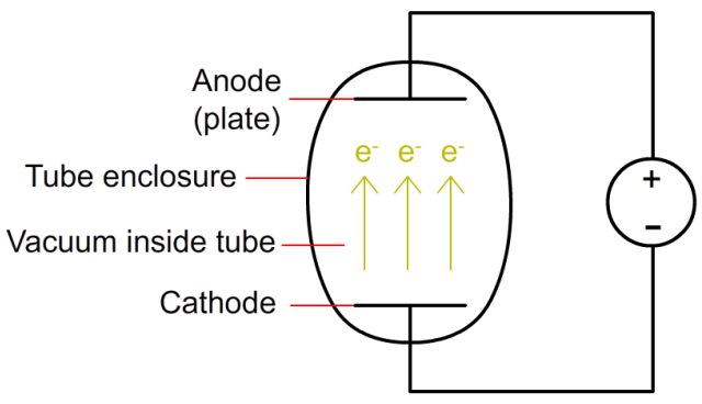
A simplified diagram of a vacuum tube diode. When the cathode is heated, and a positive voltage is applied to the anode, electrons can flow from the cathode to the anode. Note: A separate power source (not shown) is required to heat the cathode.
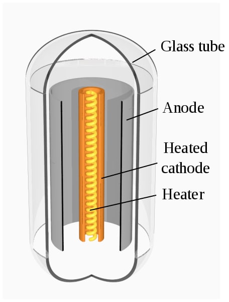
A more realistic representation of a vacuum tube diode. The electrodes are arranged as concentric cylinders within the tube, maximizing the surface area for electrons. Here, the cathode is heated by a separate heating filament, labeled Heater. (Image courtesy of Wikipedia user Svjo.)
Third Electrode’s the Charm
While diodes are quite a handy device to have around, they did not set the limit for vacuum tube functionality. In 1907, American inventor Lee de Forest added a third electrode to the mix, creating the first triode tube. This third electrode, called the control grid, enabled the vacuum tube to be used not just as a rectifier, but as an amplifier of electrical signals.
The control grid is placed between the cathode and anode, and is in the shape of a mesh (the holes allow electrons to pass through it). By adjusting the voltage applied to the grid, you can control the number of electrons flowing from the cathode to the anode. If the grid is given a strong negative voltage, it repels the electrons from the cathode and chokes the flow of current. The more you increase the grid voltage, the more electrons can pass through it, and the higher your current. In this way, the triode can serve as an on/off switch for an electrical current, as well as a signal amplifier.
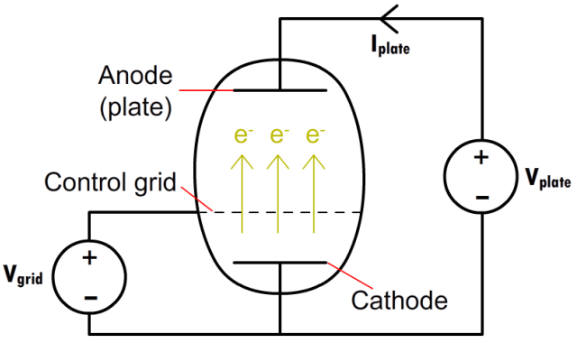
A simplified diagram of a vacuum tube triode. A minute adjustment to the grid voltage has a comparatively large effect on the plate current, allowing the triode to be used for amplification.
The evolution of triode vacuum tubes from a 1916 model (left) to one from the 1960s. (Image courtesy of Wikipedia user RJB1.)
The Transistor Is Born, but the Tube Lives On
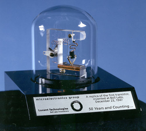
A replica of the first transistor created in 1947.
Once the transistor cat was let out of the bag, vacuum tubes were on their way to extinction in all but the most specific of applications. Transistors are much more durable (vacuum tubes, like light bulbs, will eventually need to be replaced), much smaller (imagine fitting 2 billion tubes inside an iPhone), and require much less voltage than tubes in order to function (for one thing, transistors don’t have a filament that needs heating).
Despite the emergence of the transistor, vacuum tubes aren’t completely extinct, and they remain useful in a handful of niche applications. For example, vacuum tubes are still used in high power RF transmitters, as they can generate more power than modern semiconductor equivalents. For this reason, you’ll find vacuum tubes in particle accelerators, MRI scanners, and even microwave ovens.
But perhaps the most charming modern application of vacuum tubes is in the musical community. Audiophiles swear by the quality of vacuum tube amplifiers, preferring their sound to semiconductor amps, and many professional musicians won’t consider using anything in their place.
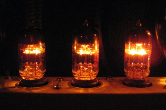
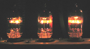
Vacuum tubes being used in a modern guitar amplifier.
 There was a time when the vacuum tube was practically synonymous with electronics. Then, about sixty years ago, semiconductors began to replace tubes in one application after another until tubes became museum pieces. But there were a few applications where tubes never fully disappeared. And recently they have been making a comeback.
When semiconductors became widely available, their advantages were immediately clear to engineers and technicians. They were smaller and lighter. They took far less power to function. They had better reliability. And probably most importantly, their characteristics were far more linear and stable.
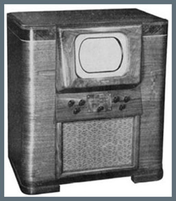 Early TV sets were large pieces of furniture with dozens of controls on them, front and back. Those controls, with odd labels such as horizontal hold and vertical linearity, were all needed in the course of an evening's viewing, since the capabilities of their components would drift with heat and time. Many a breaking news event had no video feed because it took 20 minutes to warm up and tune the cameras. In those years, TV took skill and patience, whether you were on the production side or just trying to watch.
 Transistors and integrated circuits quickly replaced tubes in consumer electronics and industrial systems until recently when something unexpected happened; certain niches began to extol the virtues of tubes. The first group was musicians and audiophiles. They claimed that tube-based amplifiers provided a sound more to their liking. Upon closer analysis, it seemed that these people had fallen in love with certain characteristics that others would term distortion; that is, the amplifier signal out was not quite the same as signal in, but instead provided the overtones that they had come to expect and value in their listening experience.
There are other areas where tubes are coming back or never totally went away. In applications where high power output is required, tubes can usually be deployed more easily that semiconductors. In applications where high radiation is present, tubes have proven more rugged. Perhaps the strangest argument in favor of tube-based apparatus is an aesthetic one. Tube equipment seems to have a distinct effect on certain technology professionals who work with them. When a vacuum tube-based chassis is in operation, its filaments produce a purposeful glow – they LOOK like they are working.
XXX . XXX Electronics/Vacuum Tubes
Flash Back
The first vacuum tube diodes were created by Thomas Edison in 1904. These initial tubes could only be used for rectification. The triode, which allowed for voltage and power amplification, was invented 3 years later in 1907 by Lee De Forest.Vacuum tubes are also referred to as thermionic tubes, thermionic valves, electron tubes, valves and just plain tubes.
While, for most electronics, vacuum tubes have been replaced by transistors, there are still some uses for which vacuum tubes are desired. Vacuum tubes are frequently used in high end Hi Fi amplifiers and are generally desirable over transistors for their "warmer" tone. They are also generally preferred in guitar amplifiers both for their smoother clipping in overdrive and the warmer tone.
Finally, vacuum tubes are used in high frequency communications (at frequencies that would destroy solid state components) as well as satellite and military communications due to their durability (they stand up to solar radiation better than solid state and are immune to electromagnetic pulse).
Passive Versus Active Components
Passive components have no gain and are not valves- Voltage Regulator: an active component which accepts a range of voltages and outputs one constant voltage.
Vacuum Tube Basics
A Vacuum Tube is a container (usually of glass) from which the air is removed. Inside the tube are two or more "Elements".- Cathode: (electron emitter) has an electrically heated filament (which you can usually see glow red ) which spits out electrons that travel through the vacuum to the Anode (electron acceptor).
- Anode (a.k.a. Plate): Is a conductive (usually metal) plate that is connected to a positive voltage. The negative electrons flow from the Cathode to the Anode.
A vacuum tube with just Cathode and Anode elements is a DIODE. Current will flow only when the Anode has a positive voltage relative to the Cathode.
- Grid(s): metal gratings or grids are placed between the Cathode and Anode to produce devices that can amplify signals.
NOTE: A tube with 3 elements (one grid) is a TRIODE, with 2 grids a TETRODE, with 3 grids a PENTODE.
A Grid between the cathode and anode controls the flow of electrons. By applying a negative voltage to the grid it is possible to control the flow of electrons. This is the basis of the Vacuum Tube amplifier.
Vacuum tubes contain heater filaments. These are similar to the filaments one would find in a standard light bulb. The filaments usually run at low voltages (6V and 12V are common, though tubes can be found with a variety of filament voltages). The filament is surrounded by a cathode. The filaments are constructed of heat the cathode to about 800 degree Celsius, at which point the cathode begins to emit electrons. The electrons normally float on the surface of the cathode and this is called a space charge. The anode is generally kept more positive than the cathode and so it draws the electrons off of the cathode.
The voltage difference in the direction from the cathode to the anode is known as the forward bias and is the normal operating mode. If the voltage applied to the Anode becomes negative relative to the Cathode, no electrons will flow. In electronics vacuum electron tube or valve is a device that controls current. Through a vacuum in sealed container. Vacuum tubes rely on thermionic emission of electrons from hot filament.
Tube Characteristics
Below is an explanation of various tube parameters:| Name | Description |
|---|---|
| Va (or Vp) | Anode(Plate) voltage (more accurately, Vak or Vpk, as it is the voltage relative to the cathode) |
| Ia (or Ip) | Anode current |
| Ra (or Rp) | Anode load resistor |
| ra (or rp) | Anode resistance (internal. Separate from and not to be confused with Ra/Rp) |
| Vg | Control grid voltage (more accurately Vgk, as it is also relative to the cathode) |
| Vk | Cathode voltage |
| Ik | Cathode current |
| Vg2 | Screen grid voltages |
| Ig2 | Screen grid current |
Diodes


As with silicon diodes, vacuum tube diodes can be used for various functions. They can be used in voltage multipliers, envelope detectors, and rectifiers, for example.
Common rectifier tubes are: 5AR4/GZ-34, 5V4-GA, GZ37, 5U4-G/GA/GB, 5Y3-G/GA, 5R4GYB, and 5R4-G/GY/GYA. Different rectifier tubes have different maximum voltages, current ratings and forward voltage drops. Some have 5V filaments and others 6.3V. And some draw more filament current than others.
Some rectifiers are half-wave (single diode) and some are full-wave, containing a single cathode, but two anodes, one for each half of the wave, as shown in the Full-wave rectifier image to the right.

Rectifier Tube Chart
| Tube Type | Max ACV | PIV | Max DCV | Max DC mA | Vf | Fil. V | Fil. mA |
|---|---|---|---|---|---|---|---|
| 5AR4-G/GY/GYA | 750 | 3100 | 358 | 250 | 67 | 5 | 2000 |
| 5AR4-GYB | 900 | 3100 | 362 | 250 | 63 | 5 | 2000 |
| 5Y3-G/GA | 350 | 1400 | 365 | 125 | 60 | 5 | 2000 |
| 5U4-GB | 450 | 1550 | 375 | 275 | 50 | 5 | 3000 |
| 5U4-G | 450 | 1550 | 381 | 225 | 44 | 5 | 3000 |
| 5U4-GA | 450 | 1550 | 381 | 250 | 44 | 5 | 3000 |
| GZ37 | 450 | 1000 | 388 | 350 | 37 | 5 | 2800 |
| 5V4-GA | 375 | 1400 | 400 | 175 | 25 | 5 | 2000 |
| 5AR4/GZ-34 | 425 | 1500 | 415 | 250 | 10 | 5 | 1900 |
| 6CA4/EZ81 | 450 | 1300 | 500 | 150 | 20 | 6.3 | 1000 |
Klystron
A klystron is a vacuum tube used for production of microwave energy. This device is related to but not the same as a magnetron. The klystron was invented after the magnetron.Klystrons work using a principle known as velocity modulation.
The klystron is a long narrow vacuum tube. There is an electron gun (heater, cathode, beam former) at one end and an anode at the other. In between is a series of donut shaped resonant cavity structures positioned so that the electron beam passes through the hole.
The first and last of the resonant cavities are electrically wired together.
At the cathode the electron beam is relatively smooth. There are natural slight increases and decreases in the electron density of the beam. As the beam passes through the holes of the resonant cavities, any changes in the electron beam cause some changes in the resting electro magnetic (EM) field of the cavities. The EM fields of the cavities begin to oscillate. The oscillating EM field of the cavities then has an effect on the electrons passing through, either slowing down or speeding up their passage.
As electrons are affected by the EM field of the first cavity they change their speed. This change in speed is called velocity modulation. By the time the electrons arrive at the last cavity there are definite groups in the beam. The groups interact strongly with the last cavity causing it to oscillate in a more pronounced way. Some of the last cavity's energy is tapped off and fed back to the first cavity to increase its oscillations. The stronger first cavity oscillations produce even stronger grouping of the electrons in the beam causing stronger oscillations in that last cavity and so on. This is positive feedback.
The output microwave energy is tapped of for use in high power microwave devices such as long range primary RADAR systems.
The klystron is a coherent microwave source in that it is possible to produce an output with a constant phase. This is a useful attribute when combined with signal processing to measure RADAR target attributes like Doppler shift.
Related microwave vacuum tubes are the Travelling Wave Tube (TWT) and the Travelling Wave Amplifier (TWA). A Hybrid device, which combines some aspects of these devices and the klystron, is a device called a Twicetron.
Magnetron
Magnetrons are used to produce microwaves.This is the original device used for production of microwaves and was invented during the Second World War for use in RADAR equipment.
Magnetrons work using a principle known as velocity modulation.
A circular chamber, containing the cathode, is surrounded by and connected to a number of resonant cavities. The walls of the chamber are the anode. The cavity dimensions determine the frequency of the output signal. A strong magnetic field is passed through the chamber, produced by a powerful magnet. The cathode is similar to most thermionic valves, except heavy, rigid construction is necessary for power levels used in most Magnetrons. Early, experimental designs used directly heated cathodes. Modern, high powered designs use a rigid, tubular cathode enclosing a heater element.
Naturally excited electrons on the surface of the cathode are drawn off, into the chamber, toward the outer walls or anode. As the electrons move out, they pass through a magnetic field that produces a force perpendicular to the direction of motion and direction of the magnetic field. The faster the electrons move, the more sideways force is produced. The result is that the electrons rotate around the central cathode as they move toward the outside of the chamber.
As electrons move past the entrances to the resonant cavities a disturbance is made to the electro magnetic (EM) field that is at rest in the cavities. The cavity begins to oscillate. When another electron moves past the cavities, it also interacts with the internal EM field. The motion of the electron can be slowed or sped up by the cavity field. As more electrons interact with the cavity EM fields, the internal cavity oscillations increase and the effect on the passing electrons is more pronounced.
Eventually, bands of electrons rotating together develop within the central chamber. Any electrons that fall behind a band are given a kick by the resonant cavity fields. Any electrons going too fast have their excess energy absorbed by the cavities. This is the velocity modulation effect. The frequency of the resonance and electron interaction is in the order of GHz. (10^9 cycles per second)
In order to have a signal output from the magnetron, one of the cavities is taped with a slot or a probe to direct energy out into a waveguide for distribution.
Magnetrons for RADARs are pulsed with short duration and high current. Magnetrons for microwave ovens are driven with a continuous lower current.
The magnetrons for WWII bombers, operated by the RAF, were sometimes taped into a shielded box so that the aircrew could heat their in-flight meals, hence the first microwave ovens.
Cathode Ray Tube
A cathode ray tube or CRT is a specialized vacuum tube in which images are produced when an electron beam strikes a phosphorescent surface. Television sets, computers, automated teller machines, video game machines, video cameras, monitors, oscilloscopes and radar displays all contain cathode-ray tubes. Phosphor screens using multiple beams of electrons have allowed CRTs to display millions of colors.The first cathode ray tube scanning device was invented by the German scientist Karl Ferdinand Braun in 1897. Braun introduced a CRT with a fluorescent screen, known as the cathode ray oscilloscope. The screen would emit a visible light when struck by a beam of electrons.
TV Tubes
TV tubes are basically cathode ray tubes. An electron beam is produced by an electrically-heated filament, and that beam is guided by two magnetic fields to a particular spot on the screen. The beam is moved so very quickly, that the eye can see not just one particular spot, but all the spots on the screen at once, forming a variable picture.- Colours are produced by having 3 or more differently coloured screen spots activated at once to a variable degree.
Oscilloscope Tubes
Oscilloscope tubes are basically the same as TV tubes, but the beam is guided by two electrostatic fields provided by internal pieces of metal. It is a necessity because an oscilloscope uses a very large range of synchronization frequencies for the deflection, when a TV set uses fixed frequencies, and it would be too difficult to drive large coils on a so large band of frequency. They are much deeper for the same screen size as a TV tube because the deflection angle is little. A TV tube has a deflection angle of 90° for the beXXX . XXX 4% zero What does solid-state mean in relation to electronics?

Three common solid state components are displayed. Clockwise from the top: inch-long circuit chip, red light-emitting diode and a transistor.
One of the first solid-state devices was a crystal radio. In a crystal radio, a piece of wire positioned on a crystal's surface is able to separate the lower-frequency audio from the higher-frequency transmitted radio carrier wave. This form of signal detection is due to the crystal's ability to pass a current in only one direction.
Solid-state gets its name from the path that electrical signals take through solid pieces of semi-conductor material. Prior to the use of solid-state devices, such as the common transistor, electricity passed through the various elements inside of a heated vacuum tube. Solid-state devices, such as a transistor, use conductors to control the flow of signals through a circuit.
- In a transistor amplifier, a small change on the input signal's amplitude is immediately reflected in larger amplitude in the output within a transistor.
- In a vacuum tube amplifier, after the tube warms up, a signal is applied to the "grid" of a tube and the resultant output of the same frequency is at a much higher amplitude.
Solid state devices called diodes have a replaced rectifier vacuum tubes, used to transform alternating current (AC) to direct current (DC). Cool-running light-emitting diodes (LEDs), another solid-state device used for indicators on the front panel of your computer and monitor, have replaced the earlier incandescent bulbs. Multiple bright LEDs are also used for the third stoplight on many U.S. vehicles and for traffic signals.
Solid-state miniature electronic components are in many places:
- Mounted on flexible thin film printed circuits in cameras and disk drives.
- The beeping sound made by a cell phone, page or auto dashboard alarm.
- The voice chip in an answering machine.
- TV remote control.
- Laser pointer.
- The inside of an MP3 player.
- A quartz watch.
- The image sensor in a digital camera and a camcorder.
- The computer monitor you are viewing.
- The mouse you will click to the next HSW screen!
XXX . XXX 4%zero null case study compare of Nano generators Work

What if we could produce electricity from the power we generate just by being alive? Imagine if you could keep your iPod charged just by tapping your fingers to the beat of the music or by wearing a hoodie with a tiny embedded circuit board that senses your pulse. Though it might sound like science fiction, nanogenerators are bringing such power sources into reality.
Nano generator is the term researchers use to describe a small electronic chip that can use mechanical movements of the body, such as a gentle finger pinch, to generate electricity . The chip has an integrated circuit etched onto a flexible surface, similar to components on the circuit boards inside your computer. As the "nano-" prefix implies, these generators are a piece of nanotechnology, or technology so small its size is measured by the nanometer (one billionth of a meter). So, even the most complex and powerful nanogenerators in existence today are small enough to be held between two fingers.
The key components inside a nanogenerator are nanowires or a similar structure made from a piezoelectric ceramic material. Piezoelectric materials can generate an electric current just by being bent or stressed. As described in How Nanowires Work, hundreds of nanowires can be packed side by side in a space less than the width of a human hair. At that scale, and with the combined flexibility of the nanogenerator's components, even the slightest movement can generate current.
Besides being incredibly small and responsive, nanogenerators are increasingly powerful. In March 2011, researchers measured the output of five nanogenerators stacked together. This tiny stack produced a current of about one microampere, which produced three volts of energy, about the same as two AA batteries .
Want to take a closer look at nano generator technology and how the practical application of nano generators will affect our lives? Let's start with some of the research behind nanogenerators.
In "The Matrix," computer-based life forms had enslaved humans on Earth and used their bodies as a power source. The humans served as the computers' limited-life batteries (batteries which can be recharged, but not indefinitely), similar to the way we'd use AA batteries in a TV remote control. Though "The Matrix" is fiction, researchers developing nanogenerators are finding reality in harnessing the body's energy to power electronic devices. that researchers must use microscopes to see what they're working on and instruments that can create and manipulate microscopic electronic components and measure their output . the first researcher using zinc oxide (ZnO) as the piezoelectric material used in the nanogenerators . the use of ZnO for their continued success in improving nanogenerators . We know piezoelectric material is the key component of a nanogenerator .
What's Happening Inside the Nanogenerator

This is a microscopic look at one of the processes used to grow ZnO nanowires. The nanowires are in the middle, growing from a chromium electrode on the left toward a gold electrode on the right.
The electricity is generated in the piezoelectric material. As mentioned before, Wang's team has used ZnO to develop nanowires. Each nanowire measures between 100 and 300 nanometers in diameter (the width of the wire). Each nanowire's length is about 100 microns; one micron = 100,000 nanometers. To put this in perspective, note that the length of the wire (not the width) is about the same as the width of two human hairs. an array of nanowires to the substrate and places a silicone electrode at the other end of the wires. The electrode has a zigzag pattern on its surface. When a small physical pressure is applied to the nanogenerator, each nanowire flexes and generates an electrical charge. The electrode captures that charge and carries it through the rest of the nanogenerator circuit. The entire nanogenerator might have several electrodes capturing power from millions of nanowires
By using nanogenerators, doctors could implant a new generation of these devices with the capacity to stay powered and last a long time with minimal body invasion . Such devices would harness the energy of involuntary movement like a heartbeat or lung expansion. In short, you could be using your body to keep alive a device that helps keep you alive in return. In addition, by using non-toxic materials like ZnO as the piezoelectric material, there is a better chance of implanting a nanogenerator without harming the body . So what's beyond medicine for nanogenerators? Researchers believe that nanogenerators could soon be powering your iPod or smartphone. Because nanogenerators are so small, they could easily be embedded in the cloth of a T-shirt or hoodie, so your iPod could use your pulse to keep its internal battery charged. Wang expects the nanogenerators his group has developed to be part of such products and available for purchase within three years .
A side benefit of using nanogenerators is their potential positive impact on the environment. Nanogenerators use a renewable resource: kinetic energy from body movement. They're created from more environmentally friendly materials than batteries, and they have the potential to reduce the waste associated with battery production and disposal. Still, the impact is small, literally, due to the size and limited power of nanogenerators. Time will tell if the nanogenerators will be viable in powering larger devices such as laptops.
Nanogenerators probably won't replace batteries, at least not in the near future. You still need battery backups for devices with which you're not in regular physical contact, such as alarm clocks. You also want to ensure that some devices continue to run idly even when you're not using or touching them, such as your smartphone. Perhaps in the future, manufacturers will pair nanogenerators with some type of rechargeable battery system to create a dependable power source with reduced environmental impact
XXX . XXX 4%zero null 0 1 From Tubes To Transistors
From UNIVAC to the latest desktop PCs, computer evolution has moved very rapidly. The first-generation computers were known for using vacuum tubes in their construction. The generation to follow would use the much smaller and more efficient transistor.
From Tubes...
Any modern digital computer is largely a collection of electronic switches. These switches are used to represent and control the routing of data elements called binary digits (or bits).Because of the on-or-off nature of the binary information and signal routing the computer uses, an efficient electronic switch was required. The first electronic computers used vacuum tubes as switches, and although the tubes worked, they had many problems.


The type of tube used in early computers was called a triode and was invented by Lee De Forest in 1906. It consists of a cathode and a plate, separated by a control grid, suspended in a glass vacuum tube. The cathode is heated by a red-hot electric filament, which causes it to emit electrons that are attracted to the plate. The control grid in the middle can control this flow of electrons. By making it negative, you cause the electrons to be repelled back to the cathode; by making it positive, you cause them to be attracted toward the plate. Thus, by controlling the grid current, you can control the on/off output of the plate.
Unfortunately, the tube was inefficient as a switch. It consumed a great deal of electrical power and gave off enormous heat—a significant problem in the earlier systems. Primarily because of the heat they generated, tubes were notoriously unreliable—in larger systems, one failed every couple of hours or so.
...To Transistors
The invention of the transistor was one of the most important developments leading to the personal computer revolution.The transistor was invented in 1947 and announced in 1948 by Bell Laboratory engineers John Bardeen and Walter Brattain. Bell associate William Shockley invented the junction transistor a few months later, and all three jointly shared the Nobel Prize in Physics in 1956 for inventing the transistor. The transistor, which essentially functions as a solid-state electronic switch, replaced the less-suitable vacuum tube. Because the transistor was so much smaller and consumed significantly less power, a computer system built with transistors was also much smaller, faster, and more efficient than a computer system built with vacuum tubes.
The conversion from tubes to transistors began the trend toward miniaturization that continues to this day. Today’s small laptop PC (or netbook, if you prefer) and even Tablet PC systems, which run on batteries, have more computing power than many earlier systems that filled rooms and consumed huge amounts of electrical power.
Although there have been many designs for transistors over the years, the transistors used in modern computers are normally Metal Oxide Semiconductor Field Effect Transistors (MOSFETs). MOSFETs are made from layers of materials deposited on a silicon substrate. Some of the layers contain silicon with certain impurities added by a process called doping or ion bombardment, whereas other layers include silicon dioxide (which acts as an insulator), polysilicon (which acts as an electrode), and metal to act as the wires to connect the transistor to other components. The composition and arrangement of the different types of doped silicon allow them to act both as a conductor or an insulator, which is why silicon is called a semiconductor.
MOSFETs can be constructed as either NMOS or PMOS types, based on the arrangement of doped silicon used. Silicon doped with boron is called P-type (positive) because it lacks electrons, whereas silicon doped with phosphorus is called N-type (negative) because it has an excess of free electrons.
MOSFETs have three connections, called the source, gate, and drain. An NMOS transistor is made by using N-type silicon for the source and drain, with P-type silicon placed in between. The gate is positioned above the P-type silicon, separating the source and drain, and is separated from the P-type silicon by an insulating layer of silicon dioxide. Normally there is no current flow between N-type and P-type silicon, thus preventing electron flow between the source and drain. When a positive voltage is placed on the gate, the gate electrode creates a field that attracts electrons to the P-type silicon between the source and drain. That in turn changes that area to behave as if it were N-type silicon, creating a path for current to flow and turning the transistor “on.”
 Cutaway view of an NMOS transistor.
A PMOS transistor works in a similar but opposite fashion. P-type silicon is used for the source and drain, with N-type silicon positioned between them. When a negative voltage is placed on the gate, the gate electrode creates a field that repels electrons from the N-type silicon between the source and drain. That in turn changes that area to behave as if it were P-type silicon, creating a path for current to flow and turning the transistor “on.”
When both NMOS and PMOS field-effect transistors are combined in a complementary arrangement, power is used only when the transistors are switching, making dense, low-power circuit designs possible. Because of this, virtually all modern processors are designed using CMOS (Complementary Metal Oxide Semiconductor) technology.
Compared to a tube, a transistor is much more efficient as a switch and can be miniaturized to microscopic scale. Since the transistor was invented, engineers have strived to make it smaller and smaller. In 2003, NEC researchers unveiled a silicon transistor only 5 nanometers (billionths of a meter) in size. Other technology, such as Graphene and carbon nanotubes, are being explored to produce even smaller transistors, down to the molecular or even atomic scale. In 2008, British researchers unveiled a Graphene-based transistor only 1 atom thick and 10 atoms (1 nm) across, and in 2010, IBM researchers created Graphene transistors switching at a rate of 100 gigahertz, thus paving the way for future chips denser and faster than possible with silicon-based designs.
Integrated Circuits: The Next Generation
The third generation of modern computers is known for using integrated circuits instead of individual transistors. Jack Kilby at Texas Instruments and Robert Noyce at Fairchild are both credited with having invented the integrated circuit (IC) in 1958 and 1959. An IC is a semiconductor circuit that contains more than one component on the same base (or substrate material), which are usually interconnected without wires. The first prototype IC constructed by Kilby at TI in 1958 contained only one transistor, several resistors, and a capacitor on a single slab of germanium, and it featured fine gold “flying wires” to interconnect them. However, because the flying wires had to be individually attached, this type of design was not practical to manufacture. By comparison, Noyce patented the “planar” IC design in 1959, where all the components are diffused in or etched on a silicon base, including a layer of aluminum metal interconnects. In 1960, Fairchild constructed the first planar IC, consisting of a flip-flop circuit with four transistors and five resistors on a circular die only about 20 mm2 in size. By comparison, the Intel Core i7 quad-core processor incorporates 731 million transistors (and numerous other components) on a single 263 mm2 die!
Birth Of The Personal Computer
The fourth generation of the modern computer includes those that incorporate microprocessors in their designs.Of course, part of this fourth generation of computers is the personal computer, which itself was made possible by the advent of low-cost microprocessors and memory.Birth of the Personal Computer
In 1973, some of the first microcomputer kits based on the 8008 chip were developed. These kits were little more than demonstration tools and didn’t do much except blink lights. In April 1974, Intel introduced the 8080 microprocessor, which was 10 times faster than the earlier 8008 chip and addressed 64 KB of memory. This was the breakthrough that the personal computer industry had been waiting for.
A company called MITS introduced the Altair 8800 kit in a cover story in the January 1975 issue of Popular Electronics. The Altair kit, considered by many to be the first personal computer, included an 8080 processor, a power supply, a front panel with a large number of lights, and 256 bytes (not kilobytes) of memory. The kit sold for $395 and had to be assembled. Assembly back then meant you got out your soldering iron to actually finish the circuit boards—not like today, where you can assemble a system of premade components with nothing more than a screwdriver.
Ed Roberts, The "Father Of The Personal Computer"
Micro Instrumentation and Telemetry Systems was the original name of the company founded in 1969 by Ed Roberts and several associates to manufacture and sell instruments and transmitters for model rockets. Ed Roberts became the sole owner in the early 1970s, after which he designed the Altair. By January 1975, when the Altair was introduced, the company was called MITS, Inc., which then stood for nothing more than the name of the company. In 1977, Roberts sold MITS to Pertec, moved to Georgia, went to medical school, and became a practicing physician. Considered by many to be the “father of the personal computer,” Roberts passed away in 2010 after a long bout with pneumonia.
The Altair included an open architecture system bus later called the S-100 bus, so named because it became an industry standard and had 100 pins per slot. The S-100 bus was widely adopted by other computers that were similar to the Altair, such as the IMSAI 8080, which was featured in the movie WarGames. The S-100 bus open architecture meant that anybody could develop boards to fit in these slots and interface to the system, and it ensured a high level of cross-compatibility between different boards and systems.The popularity of 8080 processor–based systems inspired software companies to write programs, including the CP/M (control program for microprocessors) OS and the first version of the Microsoft BASIC (Beginners All-purpose Symbolic Instruction Code) programming language.
IBM's First Personal Computer (But Not PC Compatible)
IBM introduced what can be called its first personal computer in 1975.The Model 5100 had 16 KB of memory, a built-in 16-line-by-64-character display, a built-in BASIC language interpreter, and a built-in DC-300 cartridge tape drive for storage. The system’s $8975 price placed it out of the mainstream personal computer marketplace, which was dominated by experimenters (affectionately referred to as hackers) who built low-cost kits ($500 or so) as a hobby. Obviously, the IBM system was not in competition for this low-cost market and did not sell as well by comparison.
The Model 5100 was succeeded by the 5110 and 5120 before IBM introduced what we know as the IBM Personal Computer (Model 5150). Although the 5100 series preceded the IBM PC, the older systems and the 5150 IBM PC had nothing in common. The PC that IBM turned out was more closely related to the IBM System/23 DataMaster, an office computer system introduced in 1980.In fact, many of the engineers who developed the IBM PC had originally worked on the DataMaster.
Apple's First Personal Computer (But Not Macintosh Compatible)
In 1976, a new company called Apple Computer introduced the Apple I, which originally sold for $666.66. The selling price was an arbitrary number selected by one of Apple’s cofounders, Steve Jobs. This system consisted of a main circuit board screwed to a piece of plywood; a case and power supply were not included. Only a few of these computers were made, and they reportedly have sold to collectors for more than $20 000. The Apple II, introduced in 1977, helped set the standard for nearly all the important microcomputers to follow, including the IBM PC.
The microcomputer world was dominated in 1980 by two types of computer systems. One type, the Apple II, claimed a large following of loyal users and a gigantic software base that was growing at a fantastic rate. The other type, CP/M systems, consisted not of a single system but of all the many systems that evolved from the original MITS Altair. These systems were compatible with one another and were distinguished by their use of the CP/M OS and expansion slots, which followed the S-100 standard. All these systems were built by a variety of companies and sold under various names. For the most part, however, these systems used the same software and plug-in hardware.It is interesting to note that none of these systems was PC compatible or Macintosh compatible, the two primary standards in place today.
A new competitor looming on the horizon was able to see that to be successful, a personal computer needed to have an open architecture, slots for expansion, a modular design, and healthy support from both hardware and software companies other than the original manufacturer of the system. This competitor turned out to be IBM, which was quite surprising at the time because IBM was not known for systems with these open-architecture attributes. IBM, in essence, became more like the early Apple, whereas Apple became like everybody expected IBM to be. The open architecture of the forthcoming IBM PC and the closed architecture of the forthcoming Macintosh caused a complete turnaround in the industry.
The IBM Personal Computer
At the end of 1980, IBM decided to truly compete in the rapidly growing low-cost personal computer market. The company established the Entry Systems Division, located in Boca Raton, Florida, to develop the new system. The division was intentionally located far away from IBM’s main headquarters in New York, or any other IBM facilities, so that it would be able to operate independently as a separate unit. This small group consisted of 12 engineers and designers under the direction of Don Estridge and was charged with developing IBM’s first real PC. (IBM considered the previous 5100 system, developed in 1975, to be an intelligent programmable terminal rather than a genuine computer, even though it truly was a computer.) Nearly all these engineers had come to the new division from the System/23 DataMaster project, which was a small office computer system introduced in 1980 and the direct predecessor of the IBM PC.Enter The First PC-Compatible System, Using Intel's 8088 CPU
Much of the PC’s design was influenced by the DataMaster design. In the DataMaster’s single-piece design, the display and keyboard were integrated into the unit. Because these features were limiting, they became external units on the PC, although the PC keyboard layout and electrical designs were copied from the DataMaster.
Several other parts of the IBM PC system also were copied from the DataMaster, including the expansion bus (or input/output slots), which included not only the same physical 62-pin connector, but also almost identical pin specifications. This copying of the bus design was possible because the PC used the same interrupt controller as the DataMaster and a similar direct memory access (DMA) controller. Also, expansion cards already designed for the DataMaster could easily be redesigned to function in the PC.
The DataMaster used an Intel 8085 CPU, which had a 64 KB address limit and an 8-bit internal and external data bus. This arrangement prompted the PC design team to use the Intel 8088 CPU, which offered a much larger (1 MB) memory address limit and an internal 16-bit data bus, but only an 8-bit external data bus. The 8-bit external data bus and similar instruction set enabled the 8088 to be easily interfaced into the earlier DataMaster designs.
IBM brought its system from idea to delivery of functioning systems in one year by using existing designs and purchasing as many components as possible from outside vendors. The Entry Systems Division was granted autonomy from IBM’s other divisions and could tap resources outside the company, rather than go through the bureaucratic procedures that required exclusive use of IBM resources. IBM contracted out the PC’s languages and OS to a small company named Microsoft. That decision was the major factor in establishing Microsoft as the dominant force in PC software.
Digital Research Makes Way For Microsoft
It is interesting to note that IBM had originally contacted Digital Research (the company that created CP/M, then the most popular personal computer OS) to have it develop an OS for the new IBM PC. However, Digital was leery of working with IBM and especially balked at the nondisclosure agreement IBM wanted Digital to sign. Microsoft jumped on the opportunity left open by Digital Research and, consequently, became the largest software company in the world. IBM’s use of outside vendors in developing the PC was an open invitation for the after-market to jump in and support the system—and it did.
On August 12, 1981, a new standard was established in the microcomputer industry with the debut of the IBM PC. Since then, hundreds of millions of PC-compatible systems have been sold, as the original PC has grown into an enormous family of computers and peripherals. More software has been written for this computer family than for any other system on the market.
The PC Industry 30 Years Later
In the 30 years since the original IBM PC was introduced, many changes have occurred. The IBM-compatible computer, for example, advanced from a 4.77 MHz 8088-based system to 3 GHz (3000MHz) or faster systems—about 100 000 or more times faster than the original IBM PC (in actual processing speed, not just clock speed). The original PC had only one or two single-sided floppy drives that stored 160 KB each using DOS 1.0, whereas modern systems can have several terabytes (trillion bytes) or more of hard disk storage.
A rule of thumb in the computer industry (called Moore’s Law, originally set forth by Intel cofounder Gordon Moore) is that available processor performance and disk-storage capacity doubles every one and a half to two years, give or take.
Since the beginning of the PC industry, this pattern has held steady and, if anything, seems to be accelerating.
Moore’s Law
In 1965, Gordon Moore was preparing a speech about the growth trends in computer memory and made an interesting observation. When he began to graph the data, he realized a striking trend existed. Each new chip contained roughly twice as much capacity as its predecessor, and each chip was released within 18–24 months of the previous chip. If this trend continued, he reasoned, computing power would rise exponentially over relatively brief periods.
Moore’s observation, now known as Moore’s Law, described a trend that has continued to this day and is still remarkably accurate. It was found to not only describe memory chips, but also accurately describe the growth of processor power and disk drive storage capacity. It has become the basis for many industry performance forecasts. As an example, in less than 40 years the number of transistors on a processor chip increased more than half a million fold, from 2300 transistors in the 4004 processor in 1971 to 1.17 billion transistors in the six-core versions of the Core i-series processors released in 2010.
The PC-Compatible Open Standard
In addition to performance and storage capacity, another major change since the original IBM PC was introduced is that IBM is not the only manufacturer of PC-compatible systems. IBM originated the PC-compatible standard, of course, but today it no longer sets the standards for the system it originated. More often than not, new standards in the PC industry are developed by companies and organizations other than IBM.
Today, Intel, Microsoft, and AMD are primarily responsible for developing and extending the PC hardware and software standards. Some have even taken to calling PCs “Wintel” systems, owing to the dominance of the first two companies. Although AMD originally produced Intel processors under license and later produced low-cost, pin-compatible counterparts to Intel’s 486 and Pentium processors (AMD 486, K5/K6), starting with the Athlon AMD has created completely unique processors that are worthy rivals to Intel’s own models.
In more recent years, the introduction of hardware standards such as the universal serial bus (USB), Peripheral Component Interconnect (PCI) bus, Accelerated Graphics Port (AGP) bus, PCI Express bus, ATX motherboard form factor, as well as processor socket and slot interfaces show that Intel is the driving force behind PC hardware design. Intel’s ability to design and produce motherboard chipsets as well as complete motherboards has enabled Intel processor–based systems to first adopt newer memory and bus architectures as well as system form factors. Although in the past AMD has on occasion made chipsets for its own processors, the company’s acquisition of ATI has allowed it to become more aggressive in the chipset marketplace.
PC-compatible systems have thrived not only because compatible hardware can be assembled easily, but also because the most popular OS was available not from IBM but from a third party (Microsoft). The core of the system software is the basic input/output system (BIOS); this was also available from third-party companies, such as AMI, Phoenix, and others. This situation enabled other manufacturers to license the OS and BIOS software and sell their own compatible systems. The fact that DOS borrowed the functionality and user interface from both CP/M and UNIX probably had a lot to do with the amount of software that became available. Later, with the success of Windows, even more reasons would exist for software developers to write programs for PC-compatible systems.
The Apple Macintosh Closed Standard
One reason Apple’s Macintosh systems have never enjoyed the market success of PC systems is that Apple has often used proprietary hardware and software designs that it was unwilling to license to other companies. This proprietary nature has unfortunately relegated Apple to a meager 5% market share in personal computers.
One fortunate development for Mac enthusiasts was Apple’s shift to Intel x86 processors and PC architecture in 2006, resulting in greatly improved performance and standardization as compared to the previous non-PC-compatible Mac systems. Although Apple has failed to adopt some of the industry-standard component form factors used in PCs (rendering major components such as motherboards noninterchangeable), the PC-based Macs truly are PCs from a hardware standpoint, using all the same processors, chipsets, memory, buses, and other system architectures that PCs have been using for years. I’ve had people ask me, “Is there a book like Upgrading and Repairing PCs that covers Macs instead?” Well, since 2006 Macs have essentially become PCs, they are now covered in this book by default! The move to a PC-based architecture is without a doubt the smartest move Apple has made in years—besides reducing Apple’s component costs, it allows Macs to finally perform on par with PCs.
Apple could even become a real contender in the OS arena (taking market share from Microsoft) if the company would only sell its OS in an unlocked version that would run on non-Apple PCs. Unfortunately for now, even though Apple’s OS X operating system is designed to run on PC hardware, it is coded to check for a security chip found only on Apple motherboards. There are ways to work around the check (see OSx86project.org), but Apple does not support them.
Apple’s shift to a PC-based architecture is one more indication of just how popular the PC has become. After 30 years the PC continues to thrive and prosper. With far-reaching industry support and an architecture that is continuously evolving, I would say it is a safe bet that PC-compatible systems will continue to dominate the personal computer marketplace for the foreseeable future.
Mechanical To Modern
Many discoveries and inventions have directly and indirectly contributed to the development of the PC and other personal computers as we know them today. Examining a few important developmental landmarks can help bring the entire picture into focus.The Timeline Of Computer Advancements:
The following is a timeline of significant events in computer history. It is not meant to be complete, just a representation of some of the major landmarks in computer development:
Pre-1900s: Mechanical Computers
1617: John Napier creates “Napier’s Bones,” wooden or ivory rods used for calculating.
1642: Blaise Pascal introduces the Pascaline digital adding machine.
1822: Charles Babbage introduces the Difference Engine and later the Analytical Engine, a true general-purpose computing machine.
The Early 1900s: The Vacuum Tube Era
1906: Lee De Forest patents the vacuum tube triode, used as an electronic switch in the first electronic computers.
1936: Alan Turing publishes “On Computable Numbers,” a paper in which he conceives an imaginary computer called the Turing Machine, considered one of the foundations of modern computing. Turing later worked on breaking the German Enigma code.
1936: Konrad Zuse begins work on a series of computers that will culminate in 1941 when he finishes work on the Z3. These are considered the first working electric binary computers, using electromechanical switches and relays.
1937: John V. Atanasoff begins work on the Atanasoff-Berry Computer (ABC), which would later be officially credited as the first electronic computer. Note that an electronic computer uses tubes, transistors, or other solid-state switching devices, whereas an electric computer uses electric motors, solenoids, or relays (electromechanical switches).
1943: Thomas (Tommy) Flowers develops the Colossus, a secret British code-breaking computer designed to decode teleprinter messages encrypted by the German army.
1945: John von Neumann writes “First Draft of a Report on the EDVAC,” in which he outlines the architecture of the modern stored-program computer.
1946: ENIAC is introduced, an electronic computing machine built by John Mauchly and J. Presper Eckert.
1947: On December 23, William Shockley, Walter Brattain, and John Bardeen successfully test the point-contact transistor, setting off the semiconductor revolution.
1949: Maurice Wilkes assembles the EDSAC, the first practical stored-program computer, at Cambridge University.
1950: Engineering Research Associates of Minneapolis builds the ERA 1101, one of the first commercially produced computers.
1952: The UNIVAC I delivered to the U.S. Census Bureau is the first commercial computer to attract widespread public attention.
1953: IBM ships its first electronic computer, the 701.
1954: A silicon-based junction transistor, perfected by Gordon Teal of Texas Instruments, Inc., brings a tremendous reduction in costs.
1954: The IBM 650 magnetic drum calculator establishes itself as the first mass-produced computer, with the company selling 450 in one year.
1955-1981: From Transistors In Labs, To Integrated Circuits In The Home
1955: Bell Laboratories announces the first fully transistorized computer, TRADIC.
1956: MIT researchers build the TX-0, the first general-purpose, programmable computer built with transistors.
1956: The era of magnetic disk storage dawns with IBM’s shipment of a 305 RAMAC to Zellerbach Paper in San Francisco.
1958: Jack Kilby creates the first integrated circuit at Texas Instruments to prove that resistors and capacitors can exist on the same piece of semiconductor material.
1959: IBM’s 7000 series mainframes are the company’s first transistorized computers.
1959: Robert Noyce’s practical integrated circuit, invented at Fairchild Camera and Instrument Corp., allows printing of conducting channels directly on the silicon surface.
1960: Bell Labs designs its Dataphone, the first commercial modem, specifically for converting digital computer data to analog signals for transmission across its long-distance network.
1961: According to Datamation magazine, IBM has an 81.2% share of the computer market in 1961, the year in which it introduces the 1400 series.
1964: IBM announces System/360, a family of six mutually compatible computers and 40 peripherals that can work together.
1964: Online transaction processing makes its debut in IBM’s SABRE reservation system, set up for American Airlines.
1965: Digital Equipment Corp. introduces the PDP-8, the first commercially successful minicomputer.
1969: The root of what is to become the Internet begins when the Department of Defense establishes four nodes on the ARPAnet: two at University of California campuses (one at Santa Barbara and one at Los Angeles) and one each at Stanford Research Institute and the University of Utah.
1971: A team at IBM’s San Jose Laboratories invents the 8-inch floppy disk drive.
1971: The first advertisement for a microprocessor, the Intel 4004, appears in Electronic News.
1971: The Kenbak-1, one of the first personal computers, is advertised for $750 in Scientific American.
1972: Intel’s 8008 microprocessor makes its debut.
1973: Robert Metcalfe devises the Ethernet method of network connection at the Xerox Palo Alto Research Center.
1973: The Micral is the earliest commercial, nonkit personal computer based on a microprocessor, the Intel 8008.
1973: The TV Typewriter, designed by Don Lancaster, provides the first display of alphanumeric information on an ordinary television set.
1974: Researchers at the Xerox Palo Alto Research Center design the Alto, the first workstation with a built-in mouse for input.
1974: Scelbi advertises its 8H computer, the first commercially advertised U.S. computer based on a microprocessor, Intel’s 8008.
1975: Telenet, the first commercial packet-switching network and civilian equivalent of ARPAnet, is born.
1975: The January edition of Popular Electronics features the Altair 8800, which is based on Intel’s 8080 microprocessor, on its cover.
1976: Steve Wozniak designs the Apple I, a single-board computer.
1976: The 5 1/4-inch floppy disk drive is introduced by Shugart Associates.
1977: Tandy RadioShack introduces the TRS-80.
1977: Apple Computer introduces the Apple II.
1977: Commodore introduces the PET (Personal Electronic Transactor).
1979: Motorola introduces the 68000 microprocessor.
1980: Seagate Technology creates the first hard disk drive for microcomputers, the ST-506.
1981-1995: The PC-Compatible Standard Is Entrenched
1981: Xerox introduces the Star, the first personal computer with a graphical user interface (GUI).
1981: Adam Osborne completes the first portable computer, the Osborne I, which weighs 24 pounds and costs $1795.
1981: IBM introduces its PC, igniting a fast growth of the personal computer market. The IBM PC is the grandfather of all modern PCs.
1981: Sony introduces and ships the first 3 1/2-inch floppy disk drive.
1981: Philips and Sony introduce the CD-DA (compact disc digital audio) format.
1983: Apple introduces its Lisa, which incorporates a GUI that’s similar to the one introduced on the Xerox Star.
1983: Compaq Computer Corp. introduces its first PC clone that uses the same software as the IBM PC.
1984: Apple Computer launches the Macintosh, the first successful mouse-driven computer with a GUI, with a single $1.5 million commercial during the 1984 Super Bowl.
1984: IBM releases the PC-AT (PC Advanced Technology), three times faster than original PCs and based on the Intel 286 chip. The AT introduces the 16-bit ISA bus and is the computer on which all modern PCs are based.
1985: Philips introduces the first CD-ROM drive.
1986: Compaq announces the Deskpro 386, the first computer on the market to use Intel’s 32-bit 386 chip.
1987: IBM introduces its PS/2 machines, which make the 3 1/2-inch floppy disk drive and VGA video standard for PCs. The PS/2 also introduces the MicroChannel Architecture (MCA) bus, the first plug-and-play bus for PCs.
1988: Apple cofounder Steve Jobs, who left Apple to form his own company, unveils the NeXT Computer.
1988: Compaq and other PC-clone makers develop Enhanced Industry Standard Architecture (EISA), which unlike MicroChannel retains backward compatibility with the existing ISA bus.
1988 Robert Morris’s worm floods the ARPAnet. The 23-year-old Morris, the son of a computer security expert for the National Security Agency, sends a nondestructive worm through the Internet, causing problems for about 6,000 of the 60,000 hosts linked to the network.
1989 Intel releases the 486 (P4) microprocessor, which contains more than one million transistors. Intel also introduces 486 motherboard chipsets.
1990 The World Wide Web (WWW) is born when Tim Berners-Lee, a researcher at CERN—the high-energy physics laboratory in Geneva—develops Hypertext Markup Language (HTML).
1993-2005: Windows 95 to XP, Pentiums, And Athlons
1993 Intel releases the Pentium (P5) processor. Intel shifts from numbers to names for its chips after the company learns it’s impossible to trademark a number. Intel also releases motherboard chipsets and, for the first time, complete motherboards.
1995: Intel releases the Pentium Pro processor, the first in the P6 processor family.
1995: Microsoft releases Windows 95 in a huge rollout.
1997: Intel releases the Pentium II processor, essentially a Pentium Pro with MMX instructions added.
1997: AMD introduces the K6, which is compatible with the Intel P5 (Pentium).
1998: Microsoft releases Windows 98.
1998: Intel releases the Celeron, a low-cost version of the Pentium II processor. Initial versions have no cache, but within a few months Intel introduces versions with a smaller but faster L2 cache.
1999: Intel releases the Pentium III, essentially a Pentium II with SSE (Streaming SIMD Extensions) added.
1999: AMD introduces the Athlon.
1999: The IEEE officially approves the 5 GHz band 802.11a 54 Mb/s and 2.4 GHz band 802.11b 11 Mb/s wireless networking standards. The Wi-Fi Alliance is formed to certify 802.11b products, ensuring interoperability.
2000: The first 802.11b Wi-Fi-certified products are introduced, and wireless networking rapidly builds momentum.
2000: Microsoft releases Windows Me (Millennium Edition) and Windows 2000.
2000: Both Intel and AMD introduce processors running at 1GHz.
2000: AMD introduces the Duron, a low-cost Athlon with reduced L2 cache.
2000: Intel introduces the Pentium 4, the latest processor in the Intel Architecture 32-bit (IA-32) family.
2001: The industry celebrates the 20th anniversary of the release of the original IBM PC.
2001: Intel introduces the first 2 GHz processor, a version of the Pentium 4. It takes the industry 28 1/2 years to go from 108 KHz to 1 GHz but only 18 months to go from 1 GHz to 2 GHz.
2001: Microsoft releases Windows XP, the first mainstream 32-bit operating system (OS), merging the consumer and business OS lines under the same code base (NT 5.1).
2001: Atheros introduces the first 802.11a 54 Mb/s high-speed wireless chips, allowing 802.11a products to finally reach the market.
2002: Intel releases the first 3 GHz-class processor, a 3.06 GHz version of the Pentium 4. This processor also introduces Intel’s Hyper-Threading (HT) technology, appearing as two processors to the OS.
2003-Present: Multiple CPU Cores And 64-bits
2003: Intel releases the Pentium M, a processor designed specifically for mobile systems, offering extremely low power consumption that results in dramatically increased battery life while still offering relatively high performance.
2003: AMD releases the Athlon 64, the first x86-64 (64-bit) processor for PCs, which also includes integrated memory controllers.
2003: The IEEE officially approves the 802.11g 54 Mb/s high-speed wireless networking standard.
2004: Intel introduces a version of the Pentium 4 codenamed Prescott, the first PC processor built on 90-nanometer technology.
2004: Intel introduces EM64T (Extended Memory 64 Technology), which is a 64-bit extension to Intel’s IA-32 architecture based on (and virtually identical to) the x86-64 (AMD64) technology first released by AMD.
2005: Microsoft releases Windows XP x64 Edition, which supports processors with 64-bit AMD64 and EM64T extensions.
2005: The era of multicore PC processors begins as Intel introduces the Pentium D 8xx and Pentium Extreme Edition 8xx dual-core processors. AMD soon follows with the dual-core Athlon 64 X2.
2006: Apple introduces the first Macintosh systems based on PC architecture, stating they are four times faster than previous non-PC-based Macs.
2006: Intel introduces the Core 2 Extreme, the first quad-core processor for PCs.
2006: Microsoft releases the long-awaited Windows Vista to business users. The PC OEM and consumer market releases would follow in early 2007:
2007: Intel releases the 3x series chipsets with support for DDR3 memory and PCI Express 2.0, which doubles the available bandwidth.
2007: AMD releases the Phenom processors, the first quad-core processors for PCs with all four cores on a single die.
2008: Intel releases the Core i-series (Nehalem) processors, which are dual- or quad-core chips with optional Hyper-Threading (appearing as four or eight cores to the OS) that include an integrated memory controller.
2008: Intel releases the 4x and 5x-series chipsets, the latter of which supports Core i-series processors with integrated memory controllers.
2009: Microsoft releases Windows 7, a highly anticipated successor to Vista.
2009: AMD releases the Phenom II processors in 2-, 3-, and 4-core versions.
2010: Intel releases six-core versions of the Core i-series processor (Gulftown) and a dual-core version with integrated graphics (Clarkdale). The Gulftown is the first PC processor with more than 1 billion transistors.
2010: AMD releases six-core versions of the Phenom II processor.
2011: Intel releases the second-generation Core i-series processors along with new 6-series motherboard chipsets. The chipsets and motherboards are quickly recalled due to a bug in the SATA host adapter. The recall costs Intel nearly a billion dollars and results in a several month delay in the processors and chipsets reaching the market.
XXX . XXX 4%zero null do example 6V6 6J5 Class A Vacuum Tube (Valve) Amplifier Circuit

This project involves a single ended audio amplifier, which consists of a resistive input network, a driver stage, and an output stage to a typical 8 ohm loudspeaker load, all the while, using a minimum of supportive passive components for biasing and coupling duties. Power-supply voltage is provided by full wave diode rectification of 230 VAC by a magnetic transformer. This design provides a quality audio amplifier.
Valve amplifier circuit diagram
 Amplifier Circuit Wiring Diagram")
| PARTS LIST | |
| R1 | 470Ω 1W |
| R2 | 4.7KΩ 1W |
| R3 | 1MΩ ¼W |
| R4 | 100KΩ 2W |
| R5 | 15KΩ 2W |
| R6 | 10KΩ Volume Control |
| R7 | 1kΩ ¼W |
| C1 | 33µF 250V |
| C2 | 33µF 250V |
| C3 | 0.1µF 400V |
| C4 | 10µF 250V |
| C5 | 1µF 100V |
| V1 | 6V6GT Tube |
| V2 | 6J5GT Tube |
| T1 | Audio Output Transformer, Primary 5KΩ; Secondary 8Ω |
| LS1 | 10W 8Ω Speaker |
The major factor involving the design of this single ended output stage is matching an available output tube to an available output transformer (OT) , which can provide the proper impedance matching. Using typical operating parameters, the 6V6 power tube, operating in triode mode, has an ideal load impedance of 5k Ohm, and generates about 4.5 watts of power. An OT was used, handling 8 watts and providing impedance matching from a 5k primary to an 8 ohm secondary, which is a common loudspeaker impedance.
Tube amplifier power supply

| PARTS LIST | |
| R1 | 100KΩ 3W |
| C1 | 0.047µF 400V |
| C2 | 0.047µF 400V |
| C3 | 0.22µF 1000V |
| C4 | 220µF 450V |
| D1-D4 | 1N4007 |
| F1 | 500mA Fuse |
| S1 | Switch |
| DS1 | Neon Lamp |
| T1 | Mains Transformer, Secondaries 230V, 150mA; 6.3V 3.5A |
The amplifier uses a simple linear power supply to develop 300VDC. Heater voltages are supplied directly from the 6.3VAC taps on the secondary of the power transformer. The other secondary windings, rated at 230VAC are used for the DC supply. It consists of a 4 rectifiers, variety of smoothing capacitors and resistor.
Tube Datasheets
Several construction issues were considered in the building of this amplifier. High power supply voltages, large and leaky inductive components, and high temperatures are among these considerations. I used old tube amplifier chassis.
Magnetic flux is expelled from the transformers as shown by the red arrows above. By placing the output transformer (OT) and power transformer (PT) at opposite ends of the chassis, and rotating their axes 90° from one another, induction noise from PT to OT is reduced. Although this configuration sees flux from the OT directed at the 6V6, OT flux interference into the sensitive preamp stage tube is avoided. Beneath the chassis hum reduction is further achieved by winding all pairs of wire containing AC (filament heater wires, PT primary, and secondary wiring to the diode rectifier).
Due to the 300V power supply voltages used, components were carefully chosen to withstand peak conditions.
Connect amplifier ground and power supply ground to the chassis ground point.
Mullard el84 vacuum tube

Electronic Tube Symbols
In reading or drawing radio schematic wiring diagrams, the tendency to ignore the drawn symbol and to rely upon the written designation to. explain the tube's function is very strongly manifested.
The reason for this is obvious. Many technicians and engineers lack the practice to fully interpret tube symbols and thus gain the greatest efficiency and speed in working with blueprints.
It is not always true that a tube symbol indicating a diode's function should be drawn as a diode. If the tube used is a 6Q7 and only the diode portion is used in the circuit application, the tube symbol must, none the less, be drawn representative of the 6Q7 tube.
If a tube possesses two plates for full wave rectification and only one is used as shown by the schematic, the other cannot merely be left out of the symbol, it must be shown so that the engineer or technician can tell at a glance what type of tube is actually used and can quickly estimate its operating characteristics and circuit requirements. The unconnected elements of the tube should be terminated at the circle indicating the tube's envelope.
By adhering to this method of direct representation, the possibility of errors getting by all concerned is greatly reduced.
Careful use of tube symbols will also simplify the drawing of the necessary correlated tube socket, tube base, and wiring diagrams.
If, for example, a 6X5 rectifier is drawn as a diode and marked 6X5, the reader of a schematic can usually identify the tube as possessing two plates. But if, by some error the legend "6X5" is not shown or is, accidentally written as "6Q7", the tube socket drawings, tube base diagrams and wiring diagrams may all be prepared for the 6Q7 tube's connections. Many headaches follow when eventually the error is discovered. If a tube symbol is drawn to represent a ,particular tube such confusion is reduced to a minimum.
Many tubes which have their elements internally connected are used in present day circuits. Similarly, only certain elements of other tubes are actually wired to circuit components. These are factors which must not be ignored in drawing schematics.
While it may not be essential to show unused elements and connections in a schematic they are definitely needed in wiring diagrams and tube socket drawings.
As in most things this principle of adhering too rigidly to graphical symbolism can be overdone, There are only a few basic types of tubes although the tubes of each type may run well into the hundreds. The basic types have generally recognized symbols to represent them and if these few are studied and known they will serve to reduce the major problems arising from tube symbolism in radio circuit diagrams.
The use of graphical tube symbols in actual wiring diagrams is not general practice. It is customary in this type of drawing to layout pictorially the tube socket with its pin -indicating numerals and draw the wires leading to them.
In this pictorial work the possibility of confusion is very small. Wiring diagrams are usually used in conjunction with schematics and tube socket drawings.
Tube socket drawings picture the tube base itself with call outs to indicate which prongs are "hot" and which are not used.
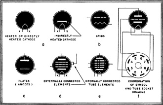
 Fig. 2 - Symbols for the commonest types of tubes. Slight modifications are needed for others. The cathode-ray tube is also shown. |
Because of the diversity of types of drawings required on various blueprints to indicate a given tube, it follows that a graphical tube symbol is a cross between a pictorial portrayal of the tube and a symbolic semi-wiring diagram of the tube itself.
At present we are concerned only with representative drawings of tube elements as they appear on a graphical symbol within the glass or metal vacuum envelope of the tube itself.
This envelope is usually indicated by a circular or oval outline and the leads from each element are carried through this circle into the wiring of the schematic itself. It is not customary procedure to indicate on the schematic that the tube is either metal or glass.
Many engineers, in drawing rough circuits, or to illustrate a point during discussions, will leave the enveloping circle of the tube's case off entirely, but in drawing a schematic to be used for production or design it is best to encircle the tube elements to avoid confusion.
As any tube will contain at least two elements and even the most complex will be confined to grids, plates, cathodes and heaters in various quantities and positions, a primary requisite is the ability to identify each tube element as shown in the symbol.
The "heaters" are usually drawn with no direct connections to their cathode. Standard methods of showing heaters are given on this page. Cathodes used in conjunction with heaters, and directly heated cathodes are also shown (Fig. 1-a).
Plates (anodes) may be drawn in any one of several ways but the illustrations given here are customary methods of representation. The commonest of these are shown in Figs. 1-b and 1-c.
A gas tube is always drawn with a distinguishing dot or circle within the tube outline and pilot lights or neon bulbs are drawn in such manner that confusion is impossible.
When tube elements are connected within the tube the symbol is drawn as indicated in Fig. 1-d, but if elements are interconnected outside of the tube's envelope, even if the interconnections are in the pins, they must be drawn external to the tube symbol, as in Fig. 1-e.
Television tubes are in a class by themselves. An example of a symbol for a television tube is shown in Fig. 2. The elements of these tubes, while similar to those of receiving and transmitting tubes, serve different purposes. Consequently the drawing of graphical symbols for television tubes should be treated and studied as a separate subject.
In graphical tube symbolism, as in all schematic drawings of radio circuits, the important thing is to standardize. Standardization of all graphical symbols and of tube symbols in particular will repay the radio engineer, draftsman or technician a hundredfold in eliminated errors and in quicker, more ready interpretation of schematic drawings.
XXX . XXX 4%zero null 0 1 2 3 4 Electronic switch
Electronic switches are devices that can stop or start an electric current as a result of the absence (or presence) of a control signal. Their invention was important in the history of computing for their use in the earliest electronic computers. In computers, electronic switches are combined to implement logic gates such as AND, OR, and NOT. These logic gates are then combined to build intermediate-level structures such as adders, multiplexors, encoders, decoders, and registers. The intermediate-level structures are then combined to create a computer processor. Besides computers, electronic switches are also used in many other devices. Three generations of electronic switches have been used in the digital computer industry.
Electromechanical relays
The earliest digital switch was the electromechanical relay, consisting of a solenoid with mechanical contact points. Relays provide a physical switch that closes when electricity animates a magnet. Early relays were slow and prone to failure due to dust in the contacts or bending of moving metal parts. Modern relays are more resilient because they are encased in housings that prevent dirt or dust from clogging the contacts, or accidental bending of armatures. However, relays are still prone to failure over time due to mechanical stress. Compared to transistors (below), they are slower, larger, and consume more power.Vacuum tubes
The vacuum tube, also called a triode, was invented in 1906 by American inventor Lee de Forest. The triode resulted from the introduction of a third electrode (called a grid) into the diode (an earlier form of vacuum tube similar to an incandescent light bulb). The triode could be used both as an amplifier (for radios) and a switch (for computers). Many of the early radio transmitters were built by de Forest using triodes, which revolutionized the field of broadcasting at the time. Radio transmission used vacuum tubes as analog devices, to modify (but not stop and start) an electrical current. Invention of the triode built upon several previous developments in physics or engineering, including the diode and the Edison effect.The ability of triode vacuum tubes to act as switches (on/off devices that stop or start an electrical current) would later be important in the building of the first electronic computers. When used as an "on/off" switch in a computer, vacuum tubes were also sometimes called electron valves, or just valves. Unlike relays, vacuum tubes expose no physical armature contacts to break or get dirty, and they are faster than relays. But they also cost a lot to manufacture, consume a lot of power, give off a great deal of heat, and tend to burn out often.
Gas tubes
Tubes filled with gas rather than evacuated to vacuum are used for specialized applications, typically involving high power, such as the krytron.Transistors
In the 1950's the Bipolar junction transistor (or BJT) was invented at AT&T Bell Laboratories in 1948 by John Bardeen, Walter Brattain, and William Shockley (all of whom shared the Nobel prize for physics in 1956 for the transistor's invention). This type of transistor still is widely used today. Today's most-used transistor is the Metal Oxide Semiconductor Field Effect Transistor (MOSFET), present by the millions in integrated circuits. This transistor was invented by Dawon Khang and Martin Atalla in 1960, another Bell Labs research team.
Transistors perform operations earlier provided by vacuum tubes, but are smaller, cheaper, require less power, and obtain faster switching times. The first transistor was made from materials that included a paper clip and a razor blade.
Although transistors can be manufactured as stand-alone devices, more often they are encapsulated inside small, semiconductor chips (often called integrated circuits, or simply IC's). When technology advanced to the point where millions of transistors could be packed onto an IC the size of a fingernail, the density of transistors on the chip came to be called VLSI (Very Large Scale Integration). The density of transistors in silicon chips has been predicted effectively by Moore's law, illustrated by the density of switching elements in these computer processors:
Eniac (room sized):  19,500 vacuum tubes and relays
Intel 8088 processor (2 inches long):  29,000 transistors
Intel Pentium II processor (5 inches long):   7  million transistors
Intel Pentium III processor:  28 million transistors
Intel Pentium 4 processor:  42 million transistors
XXX . XXX 4%zero null 0 1 2 3 4 5 Slapper detonator
One of the attractions of slapper detonators, which evolved from exploding bridge wire (EBW) detonators, first designed by Luis Alvarez duing the Manhattan Project, is that they are both extremely fast, and multiple detonators can be exploded in synchrony, or after controlled delays. They were developed at Lawrence Livermore National Laboratory as a second step built on the EBW detonator. The slapper uses the expanding foil plasma to drive a second foil or plastic film to "slap" the actual detonator, at extreme speed, into the explosive surface. It may be propelled completely by the plasma, but advanced designs use a magnetic field to supplement its speed. "Slappers are fairly efficient at converting electrical energy into flyer kinetic energy, it is not hard to achieve 25-30% energy transfer.
The heart of a slapper detonator is a high-density explosive pellet, possibly a plastic bonded explosive, pressed against an insulating disk with a hole in its center.
Against the disk is place the flying "slapper", made of a strong plastic such as Kapton or Mylar, covered with etched metal foil on one side. "A necked down section of the etched foil acts as the bridgewire. The high current firing pulse causes vaporization of the necked down section of the foil. This then shears the insulated flyer which accelerates down the barrel of the disk and impacts the explosive pellet. This impact energy transmits a shock wave into the explosive causing it to detonate."
Since the slapper has appreciable two-dimensional aspects compared to an exploding wire, it can initiate an area, not a line or point, of the explosive.
Industrial and military uses are growing increasingly widespread. Versions, packaged in common integrated circuit containers and suitable for inclusion in military-grade printed circuit boards, are used in such applications as anti-tank missiles.
A slapper detonator has been used as part of a high-speed, one-shot electronic switch
+++++++++++++++++++++++++++++++++++++++++++++++++++++++++++++++++++++++
ELECTRONIC SWITCH ( Short Wave Interaction To Couple Highway ) ingredients :
++++++++++++++++++++++++++++++++++++++++++++++++++++++++++++++++++++++
Tidak ada komentar:
Posting Komentar