A WORD FROM ME
when I studied in electronics engineering at the undergraduate level there I knew and could understand that electronic engineering is a pure technique that I have learned myself from the analysis and evidence of self-taught practice in my home; at that time I saw that electronics science can not be understood only from a technical drawing and its symbol symbol on the drawing paper but an electronics engineer is forced to and can and is able to engineer a device and electronic engineering material that is structured to fit the desired function and requirement by us as individuals, groups or wider needs of the earth; in the field of electronics engineering unlike other fields of the field such as building or civil engineering --- architectural engineering --- mapping techniques (geodesy and geology) --- mechanical engineering ---- and new electrical engineering branches of informatics engineering; in engineering electronics engineering drawing --- components --- raw materials --- design process --- analysis of both software and brainware --- scale comparison --- component replacement (component equation) --- installation of components on PCB (both with the latest solder or technique that is SMT technique until nano technology) --- the quality of the component materials used --- the installation robotic versus humans -----> it is interrelated and determine the results of the process and performance of tools and materials desired by user. when I graduate college and even college hardware design equivalent Post-graduate (S-2) for 1 year I researched by using existing equipment at that time in my study and work at home that the performance of an electronic device can not be done only from the above count paper drawing design but after we compute in theory electronics circuit theory studied in lectures and books electronic books such as electronic principles principles (Malvino) as well as integrated electronic circuit (milmann halkias) there we are constrained in placing components of electronic components according to the image or design that we make as you wish or user; in which the installed component must be exactly the same as the drawing of the design we made - numerical analysis - as well as the circuit count theory (node - mesh - norton - thevenin - superposition - lineiritas Analysis etc) - function of mathematical function of transformation analysis like laplace - fourier - differential - integral - jacobian - etc as comparative study we have to install component good and ideal maybe according to count and circuit design analysis .
Design of electronic devices (Hardware design) = Performance of components and materials of electronics .
Electronic Engineering = Pure Technique
XXX . XXX stack pointer
A stack pointer is a small register that stores the address of the last program request in a stack. A stack is a specialized buffer which stores data from the top down. As new requests come in, they "push down" the older ones. The most recently entered request always resides at the top of the stack, and the program always takes requests from the top.
A stack (also called a pushdown stack) operates in a last-in/first-out sense. When a new data item is entered or "pushed" onto the top of a stack, the stack pointer increments to the next physical memory address, and the new item is copied to that address. When a data item is "pulled" or "popped" from the top of a stack, the item is copied from the address of the stack pointer, and the stack pointer decrements to the next available item at the top of the stack.
A stack is a LIFO (last in, first out - the last entry you push on to the stack is the first one you get back when you pop) data structure that is typically used to hold stack frames (bits of the stack that belong to the current function).
This includes, but is not limited to:
- the return address.
- a place for a return value.
- passed parameters.
- local variables.
The actual implementation of a stack depends on the microprocessor architecture. It can grow up or down in memory and can move either before or after the push/pop operations.
Operation which typically affect the stack are:
- subroutine calls and returns.
- interrupt calls and returns.
- code explicitly pushing and popping entries.
- direct manipulation of the SP register.
Consider the following program in my (fictional) assembly language:
Addr  Opcodes   Instructions    ; Comments
----  --------  --------------  ----------
                                ; 1: pc<-0000, sp<-8000
0000  01 00 07  load r0,7       ; 2: pc<-0003, r0<-7
0003  02 00     push r0         ; 3: pc<-0005, sp<-7ffe, (sp:7ffe)<-0007
0005  03 00 00  call 000b       ; 4: pc<-000b, sp<-7ffc, (sp:7ffc)<-0008
0008  04 00     pop r0          ; 7: pc<-000a, r0<-(sp:7ffe[0007]), sp<-8000
000a  05        halt            ; 8: pc<-000a
000b  06 01 02  load r1,[sp+2]  ; 5: pc<-000e, r1<-(sp+2:7ffe[0007])
000e  07        ret             ; 6: pc<-(sp:7ffc[0008]), sp<-7ffe
- This is the starting condition where the program counter is zero and the stack pointer is 8000 (all these numbers are hexadecimal).
- This simply loads register r0 with the immediate value 7 and moves to the next step (I'll assume that you understand the default behavior will be to move to the next step unless otherwise specified).
- This pushes r0 onto the stack by reducing the stack pointer by two then storing the value of the register to that location.
- This calls a subroutine. What would have been the program counter is pushed on to the stack in a similar fashion to r0 in the previous step and then the program counter is set to its new value. This is no different to a user-level push other than the fact it's done more as a system-level thing.
- This loads r1 from a memory location calculated from the stack pointer - it shows a way to pass parameters to functions.
- The return statement extracts the value from where the stack pointer points and loads it into the program counter, adjusting the stack pointer up at the same time. This is like a system-level pop (see next step).
- Popping r0 off the stack involves extracting the value from where the stack pointer points then adjusting that stack pointer up.
- Halt instruction simply leaves program counter where it is, an infinite loop of sorts
Hopefully from that description, it will become clear. Bottom line is: a stack is useful for storing state in a LIFO way and this is generally ideal for the way most microprocessors do subroutine calls.
Just to clarify the steps taken when pushing and popping values in the above example (whether explicitly or by call/return), see the following examples:
LOAD R0,7
PUSH R0
                     Adjust sp       Store val
sp-> +--------+      +--------+      +--------+
     |  xxxx  |  sp->|  xxxx  |  sp->|  0007  |
     |        |      |        |      |        |
     |        |      |        |      |        |
     |        |      |        |      |        |
     +--------+      +--------+      +--------+

POP R0
                     Get value       Adjust sp
     +--------+      +--------+  sp->+--------+
sp-> |  0007  |  sp->|  0007  |      |  0007  |
     |        |      |        |      |        |
     |        |      |        |      |        |
     |        |      |        |      |        |
     +--------+      +--------+      +--------+
To push a value onto the stack, the stack pointer is incremented to point to the next physical memory address, and the new value is copied to that address in memory.
To pop a value from the stack, the value is copied from the address of the stack pointer, and the stack pointer is decremented, pointing it to the next available item in the stack.
The most typical use of a hardware stack is to store the return address of a subroutine call. When the subroutine is finished executing, the return address is popped off the top of the stack and placed in the Program Counter register, causing the processor to resume execution at the next instruction following the call to the subroutine.
The Stack Pointer is a register which holds the address of the next available spot on the stack.
The stack is a area in memory which is reserved to store a stack, that is a LIFO (Last In First Out) type of container, where we store the local variables and return address, allowing a simple management of the nesting of function calls in a typical program.
For 8085: Stack pointer is a special purpose 16-bit register in the Microprocessor, which holds the address of the top of the stack.
The stack pointer register in a computer is made available for general purpose use by programs executing at lower privilege levels than interrupt handlers. A set of instructions in such programs, excluding stack operations, stores data other than the stack pointer, such as operands, and the like, in the stack pointer register. When switching execution to an interrupt handler on an interrupt, return address data for the currently executing program is pushed onto a stack at the interrupt handler's privilege level. Thus, storing other data in the stack pointer register does not result in stack corruption. Also, these instructions can store data in a scratch portion of a stack segment beyond the current stack pointer.
The Stack is an area of memory for keeping temporary data. Stack is used by the CALL instruction to keep the return address for procedures The return RET instruction gets this value from the stack and returns to that offset. The same thing happens when an INT instruction calls an interrupt. It stores in the Stack the flag register, code segment and offset. The IRET instruction is used to return from interrupt call.
The Stack is a Last In First Out (LIFO) memory. Data is placed onto the Stack with a PUSH instruction and removed with a POP instruction. The Stack memory is maintained by two registers: the Stack Pointer (SP) and the Stack Segment (SS) register. When a word of data is PUSHED onto the stack the the High order 8-bit Byte is placed in location SP-1 and the Low 8-bit Byte is placed in location SP-2. The SP is then decremented by 2. The SP addds to the (SS x 10H) register, to form the physical stack memory address. The reverse sequence occurs when data is POPPED from the Stack. When a word of data is POPPED from the stack the the High order 8-bit Byte is obtained in location SP-1 and the Low 8-bit Byte is obtained in location SP-2. The SP is then incremented by 2.
The stack pointer holds the address to the top of the stack. A stack allows functions to pass arguments stored on the stack to each other, and to create scoped variables. Scope in this context means that the variable is popped of the stack when the stack frame is gone, and/or when the function returns. Without a stack, you would need to use explicit memory addresses for everything. That would make it impossible (or at least severely difficult) to design high-level programming languages for the architecture. Also, each CPU mode usually have its own banked stack pointer. So when exceptions occur (interrupts for example), the exception handler routine can use its own stack without corrupting the user process.
On some CPUs, there is a dedicated set of registers for the stack. When a call instruction is executed, one register is loaded with the program counter at the same time as a second register is loaded with the contents of the first, a third register is be loaded with the second, and a fourth with the third, etc. When a return instruction is executed, the program counter is latched with the contents of the first stack register and the same time as that register is latched from the second; that second register is loaded from a third, etc. Note that such hardware stacks tend to be rather small (many the smaller PIC series micros, for example, have a two-level stack).
While a hardware stack does have some advantages (push and pop don't add any time to a call/return, for example) having registers which can be loaded with two sources adds cost. If the stack gets very big, it will be cheaper to replace the push-pull registers with an addressable memory. Even if a small dedicated memory is used for this, it's cheaper to have 32 addressable registers and a 5-bit pointer register with increment/decrement logic, than it is to have 32 registers each with two inputs. If an application might need more stack than would easily fit on the CPU, it's possible to use a stack pointer along with logic to store/fetch stack data from main RAM.
Stack register A stack register is a computer central processor register whose purpose is to keep track of a call stack. On an accumulator-based architecture machine, this may be a dedicated register such as SP on an Intel x86 machine. On a general register machine, it may be a register which is reserved by convention, such as on the PDP-11 or RISC machines. Some designs such as the Data General Eclipse had no dedicated register, but used a reserved hardware memory address for this function.
Machines before the late 1960s—such as the PDP-8 and HP 2100—did not have compilers which supported recursion. Their subroutine instructions typically would save the current location in the jump address, and then set the program counter to the next address. While this is simpler than maintaining a stack, since there is only one return location per subroutine code section, there cannot be recursion without considerable effort on the part of the programmer.
A stack machine has 2 or more stack registers — one of them keeps track of a call stack, the other(s) keep track of other stack(s).
Stack registers in x86
In 8086, the main stack register is called stack pointer - SP. The stack segment register (SS) is usually used to store information about the memory segment that stores the call stack of currently executed program. SP points to current stack top. By default, the stack grows downward in memory, so newer values are placed at lower memory addresses. To push a value to the stack, thePUSH instruction is used. To pop a value from the stack, the POP instruction is used.Example: Assuming that SS = 1000h and SP = 0xF820. This means that current stack top is the physical address 0x1F820 (this is due to memory segmentation in 8086). The next two machine instructions of the program are:
PUSH AX
PUSH BX
- These first instruction shall push the value stored in AX (16-bit register) to the stack. This is done by subtracting a value of 2 (2 bytes) from SP.
- The new value of SP becomes 0xF81E. The CPU then copies the value of AX to the memory word whose physical address is 0x1F81E.
- When "PUSH BX" is executed, SP is set to 0xF81C and BX is copied to 0x1F81C.
POP BX
POP AX
POP BXcopies the word at 0x1F81C (which is the old value of BX) to BX, then increases SP by 2. SP now is 0xF81E.POP AXcopies the word at 0x1F81E to AX, then sets SP to 0xF820.
NOTE: In 8086,
PUSH & POP instructions can only work with 16-bit elements.Stack engine
Simpler processors store the stack pointer in a regular hardware register and use the arithmetic logic unit (ALU) to manipulate its value. Typically push and pop are translated into multiple micro-ops, to separately add/subtract the stack pointer, and perform the load/store in memory.Newer processors contain a dedicated stack engine to optimize stack operations. Pentium M was the first x86 processor to introduce a stack engine. In its implementation, the stack pointer is split among two registers: ESPO, which is a 32-bit register, and ESPd, an 8-bit delta value that is updated directly by stack operations. PUSH, POP, CALL and RET opcodes operate directly with the ESPd register. If ESPd is near overflow or the ESP register is referenced from other instructions (when ESPd ≠ 0), a synchronisation micro-op is inserted that updates the ESPO using the ALU and resets ESPd to 0. This design has remained largely unmodified in later Intel processors, although ESPO has been expanded to 64 bits.
A stack engine similar to Intel's was also adopted in the AMD K8 microarchitecture. In Bulldozer, the need for synchronization micro-ops was removed, but the internal design of the stack engine is not known
What is a “stack pointer” in a microprocessor?
the “stack” is a block of random-access memory (RAM) for storage of data or addresses, and is usually organized as a series of either “top-down” or “bottom-up” locations. The “stack pointer” is a special function register that “points to” (contains the address of) a location within the block, and is used along with special instructions to access the stack contents:
- The PUSH instruction places data into the location pointed to by the stack pointer, and then causes the stack pointer’s value to be incremented (for a “bottom-up” stack) or decremented (for a “top-down”) stack.
- The POP instruction takes data from the location pointed to by the stack pointer, and then causes the stack pointer’s value to be decremented (for a “bottom-up” stack) or incremented (for a “top-down” stack).
Other instructions (particularly those associated with interrupt handling) may modify the stack pointer’s value, so programmers using low-level (i.e. assembly) languages to program the microprocessor must be careful when performing stack operations. Some microprocessors will set an error flag if the stack pointer goes above (stack overflow) or below (stack underflow) pre-defined values, but the implementation of these - and other - flags is specific to the particular microprocessor. For many systems the stack is a relatively small amount of the total amount of RAM, so additional care is required to guard against stack errors. This can be important for programs that require recursive operations, so stack size is often a critical factor in determining maximum recursion depth in many systems.
There is so much more that can be said about stacks, even though their operation is fundamentally quite simple
a stack is an abstract data type that serves as a collection of elements, with two principal operations:
- push, which adds an element to the collection, and
- pop, which removes the most recently added element that was not yet removed.
The order in which elements come off a stack gives rise to its alternative name, LIFO (last in, first out).
You can consider it as extra space to store your register data when you get short with the limited number of general purpose registers.
Similarly,
With respect to the Intel 8085 microprocessor, a Stack Pointer points to the top of the Stack. The Physical address of Stack(SP) is declared by the programmer using the LXI SP command in Intel 8085.
LXI SP, 4000 H. (H - Hexadecimal)
SP is a 16-bit register in Intel 8085 microprocessor and hence takes 2 bytes of data as input.
At times, you may feel that the number of general purpose registers is not sufficient to calculate your answer and you have to free some of the general purpose registers for your further calculation or you immediately want to store a important data then you can store your registers information in the stack(using PUSH) and also retrieve the information from the stack(using POP) when needed.
PUSH Operation in Intel 8085 takes 2 bytes as input and always occurs in register pairs( PSW & Accumulator, B & C, D & E, H & L). First the data of the Higher byte is stored then the Lower byte.
LXI SP, 4000 H
PUSH B
The data stored in Register B is stored in the Stack(4000 H) first then the value of Stack Pointer is decremented(3FFF H) and data stored in Register C is stored in Stack.
Similarly in the POP command of Intel 8085.
XXX . XXX 4% zero AVR Stack & Stack Pointer
What is a stack?
A stack is a consecutive block of data memory allocated by the programmer. This block of memory can be use both by the microcontroller internal control as well as the programmer to store data temporarily. The stack operates with a Last In First Out (LIFO) mechanism, i.e the last thing store on the stack is the first thing to be retrieved from the stack.What is the Stack Pointer?
The stack pointer is basically a register or registers that holds either "the memory address of the last location on that stack where data was stored" or "the memory address of the next available location on the stack to store data." The definition of the stack pointer depends on the design of the microcontroller.In AVR microcontrollers, such as the ATMega8515, ATMega16, ATTiny13, etc., the stack pointer holds the address on the next available location on the stack available to store data.
The AVR Stack Pointer
The AVR 8-bits microcontroller stack pointer can either consist of a single I/O register SPL (Stack Pointer Low) or two (2) I/O registers SPL and SPH (Stack Pointer High). The size of the stack pointer depends on the amount of data memory a microntroller contains. If the entire data memory can be addressed using 8-bits then the stack pointer is 8-bits wide i.e. SPL only, otherwise the stack pointer is consist of SPL and SPH.
Setting-up the AVR Stack
A programmer set up the stack on a microcontroller by loading the start address of the stack into the microcontroller stack pointer. The code below shows how to set up the stack in an AVR ATMega8515 microcontroller. Here the address being loaded is that of the last memory location in SRAM. This code could also be used for the ATMega16 , ATMega32 or any one of the AVR microcontrooler with a 16-bits stack pointer, you just of the replace the "m8515def.inc" include file with "m16def.inc" or "m32def.inc" respectively.
Notes:
- RAMEND is a label that represents the address of the last memory location in SRAM. To use this label you MUST ensure that you include the definition header file for the specific microcontroller.
- The functions low() and high() are use by the assembler to return the low byte and high byte respectively of a 16-bit word. Remember we are dealing with a 8-bit microcontroller which can only handle only 8-bits at a time. RAMEND is a 16-bit word and so we use the functions to split it.
.include "m8515def.inc"

		LDI	R16, low(RAMEND)
		OUT	SPL, R16
		LDI	R16, high(RAMEND)
		OUT	SPH, R16
AVR Microcontroller's Stack Operation
As mentioned earlier the stack can be use by both the microcontroller internal control and the programmer. The programmer accesses the stack using the PUSH and POP instructions. The PUSH instruction is use to store data on the stack while the POP instruction is used to retrieve data from the stack. The operation of the AVR stack will be discussed using the code that follows.
Notes:
Notice here the microcontroller being used in the code below is the Atmel ATTiny2313 AVR microcontroller. This AVR microcontroller's data memory can be addressed using 8-bits and therefore its stack pointer is defined only by the SPL.
/*
 *  Compatibly in both AVR Studio 5 & AVR Studio 6
 *
 *  Created: 10/15/2011 2:44:24 PM
 *  Author: AVR Tutorials
 */

.include "tn2313def.inc"

	;Set up AVR ATTiny2313 stack
	LDI	R16, RAMEND
	OUT	SPL, R16

	LDI	R16, 0x33
	LDI	R17, 0x25
	LDI	R18, 0x0A

	PUSH	R16
	PUSH	R17
	POP	R17
	PUSH	R18


end:	RJMP	end
 Figure 1 - Initial Stack |  Figure 2 - Stack After First PUSH |
 Figure 3 - Stack After Second PUSH |  Figure 4 - Stack After POP |
 Figure 5 - Stack After Third PUSH |  |
stack pointer Often used in computer programming, the stack pointer refers to a cutoff point for relevance in a stack of memory. This point is the smallest address, anything smaller is seen as garbage and higher, valid data.
How do you transform that Idea into a product that you can market and sell? How do you make the hardware? Create a schematic symbol and capture the design? What is PCB layout, and why do I need a Gerber file? Can I simulate the design before I build it? How long does it take to design a simple board? How much does it cost to fabricate a PCB? How much to assemble it with the components?There are a lot of questions in the design process .

Creating An Assembled Board
The flowchart below shows the basic stages an Idea goes through to becoming a tangible reality. In this article, we focus on the Hardware part of product development. Please refer to the other articles in this series for explanations of Software, User Application and Testing.
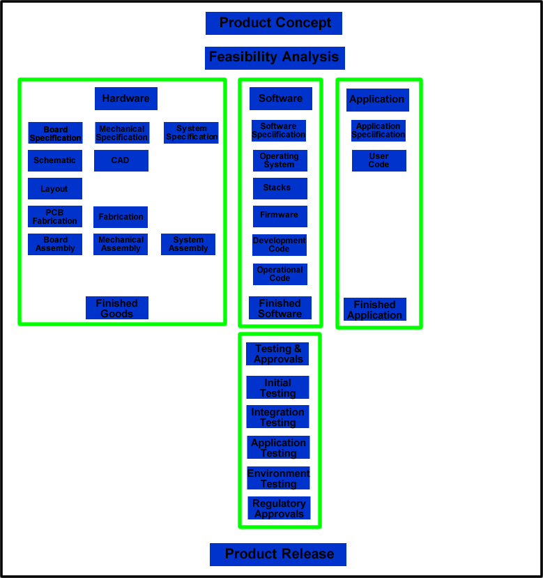
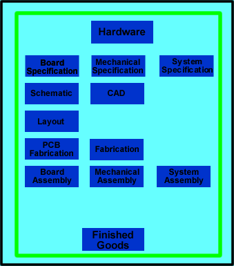
The Hardware block is expanded below for easier reference. This is a high-level diagram of the basic flow to create electronics; The nearly a dozen stages indicated in the diagram could have multiple sub-stages, depending on the design complexity and requirements.
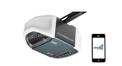
To illustrate this process, we’ll use the Idea of a smart garage door opener. The idea is that a homeowner wants to use a smart-phone to check if the home garage door is opened or closed. The homeowner would also like to be able to remotely open or close the door with the smart-phone. For example, to let a guest in or a child that forgot/lost a key.
Referring back to the flow chart diagram at the beginning of this article, the Idea needs to be conceptualized so that it can be shared with everyone that will be working on it. The Concept set out what the idea is, what it does, who will use it and in what context. Even if it’s just you, it still important to write out and document the Concept so you can focus on specifics. This is the starting point for the requirements of the idea.
The Concept is very similar to the idea, but with added details and refinement: A garage door opener that is powered with standard US 120V, 10A circuit. It should have a wired push-button to open/close manually, an integrated light fixture and safety sensor inputs (e.g., doesn’t close if something/someone is in the way). Should be able to handle single wide and double wide doors. It connects wirelessly with a smart-phone (Apple/iOs or Android, no Windows, Blackberry or Others). As this is a fairly generalized description, it shouldn’t take more than 1 hour to write out a Concept of a thought out Idea.
Next is to do an Analysis or Feasibility study. This is where you investigate all the possible (and even the impossible) ways you can realize the idea. It’s best to partition the concept in various blocks or modules to make the analysis more cohesive. Some major blocks in this Concept for a smart garage door opener are Motor, Lighting, Power, Communications, Enclosure, Controls.
It’s worth emphasizing that at this initial stage, all the various possibilities should be taken into account, researched and explored. Nothing should be dismissed. The Feasibility process is to document the findings, and then rank them; Pick the top candidate as the “recommendation” for going forward.
Let’s dive into the Communications: Should the device have wired or wireless capabilities? There are many wireless communications methods available including Cellular, Radio, WiFi, WiMax, Bluetooth, Zigbee and others. Wired solutions could include standard Ethernet or Ethernet-Over-Powerline. Each of these should be examined to determine if it would meet the requirements, what are the advantages and disadvantages for each, the availability and cost. Other things for consideration may include the size, weight, power usage, and regulatory compliances.
For a smaller, not too complicated product (and these metrics of course depend on your background, experience with similar products, and many other factors) budget about 45 hours for the Feasibility study. This may seem like a large up-front time investment, but being thorough at the beginning pays off huge dividends as the project progresses. The cost for making changes at this stage is also very low; The cost increases exponentially with each stage.
As an example: Imagine the scenario where you launch the product – Yay! A happy homeowner buys your smart garage door opener and has just paid the installer to put it. The homeowner launches the smart-phone app but can’t “find” the garage door opener. After a long talk with your (expensive) help support tech, the problem is found out that opener is “too far away” to communicate.
No longer a happy homeowner when it comes to your product (and you can be sure you’ll hear about it on Twitter, Facebook and Yelp). You have to take a return on the opener and reimburse the owner for the cost of the installation/removal. Expensive! And you find out that as more customers buy and install the open, more than half have the same problem. This means a recall and redesign. Which could have been avoided by a thorough and detailed investigation during the Feasibility stage.
Having completed the Feasibility study and defined solid recommendations for how to meet the Concept requirements, the next phase involves defining the Hardware, Software and User Application.
These items can be put into sub-groups under hardware: Board Specification, Mechanical Specification and System Specification. Now let’s look at each of these in a little more detail.
From this specification, a System Bill Of Materials (BOM) is created which lists every unique item: a description of what it is, the vendor, the vendor part number, an optional internal part number and a placement designator. The BOM is used by the purchasing department to buy the necessary amount of materials to build the unit, and by the manufacturing group to know how to assemble it. For some products there literally no items that would be included in this specification, and for other products this is the only specification when they are built completely using COTS. I budget 15 hours on average for developing this specification.
The CAD files are sent to the fabricator who cuts, bends, stamps, drills and otherwise works on the metal to create what is on the drawings. Similarly, a product may use a 3-D Printing (an additive process) or a CNC milling-machine (a subtractive process) to create pieces of the product. Rapid prototype companies can provide quick turn-around of low volumes in 1 to 3 days, but creating mechanical pieces can often take 1 to 3 weeks.
If you are not familiar with all the types of components available to you as a designer, there is a helpful 3-Volume Encyclopedia of Electronic Components that set includes key information on electronics parts for your projects—complete with photographs, schematics, and diagrams.
Once you understand the components, here is an excellent reference provides the essential information that every circuit designer needs to produce a working circuit, as well as information on how to make a design that is robust, tolerant to noise and temperature, and able to operate in the system for which it is intended. It looks at best practices, design guidelines, and engineering knowledge gained from years of experience, and includes practical, real-world considerations for components and printed circuit boards (PCBs) as well as their manufacturability, reliability, and cost:
Of particular importance is the pin-out (e.g., what each pin or connection of a device actual does) for the components. Also included is the power usage and timing information. It’s also useful to include the device sizes (e.g., width, length, height and weight) for reference. How each device is used and how it connects with other devices on the board is described in this document. As such, the board specification is used as the guidelines for the schematics.
This is a rather detailed document; It can take 40 hours to read through data sheets and determine how devices work together. In the case of our garage door opener example, how does the processor on the board control the motor to turn the gears which opens/closes the door? How does the door status get read from a sensor and sent to the communications chip? All of the signals travel on wires / board traces to the pins of chips and the designer has to determine which pins and wires are connected.
The Hardware block is expanded below for easier reference. This is a high-level diagram of the basic flow to create electronics; The nearly a dozen stages indicated in the diagram could have multiple sub-stages, depending on the design complexity and requirements.
To illustrate this process, we’ll use the Idea of a smart garage door opener. The idea is that a homeowner wants to use a smart-phone to check if the home garage door is opened or closed. The homeowner would also like to be able to remotely open or close the door with the smart-phone. For example, to let a guest in or a child that forgot/lost a key.
Referring back to the flow chart diagram at the beginning of this article, the Idea needs to be conceptualized so that it can be shared with everyone that will be working on it. The Concept set out what the idea is, what it does, who will use it and in what context. Even if it’s just you, it still important to write out and document the Concept so you can focus on specifics. This is the starting point for the requirements of the idea.
The Concept is very similar to the idea, but with added details and refinement: A garage door opener that is powered with standard US 120V, 10A circuit. It should have a wired push-button to open/close manually, an integrated light fixture and safety sensor inputs (e.g., doesn’t close if something/someone is in the way). Should be able to handle single wide and double wide doors. It connects wirelessly with a smart-phone (Apple/iOs or Android, no Windows, Blackberry or Others). As this is a fairly generalized description, it shouldn’t take more than 1 hour to write out a Concept of a thought out Idea.
Next is to do an Analysis or Feasibility study. This is where you investigate all the possible (and even the impossible) ways you can realize the idea. It’s best to partition the concept in various blocks or modules to make the analysis more cohesive. Some major blocks in this Concept for a smart garage door opener are Motor, Lighting, Power, Communications, Enclosure, Controls.
It’s worth emphasizing that at this initial stage, all the various possibilities should be taken into account, researched and explored. Nothing should be dismissed. The Feasibility process is to document the findings, and then rank them; Pick the top candidate as the “recommendation” for going forward.
Let’s dive into the Communications: Should the device have wired or wireless capabilities? There are many wireless communications methods available including Cellular, Radio, WiFi, WiMax, Bluetooth, Zigbee and others. Wired solutions could include standard Ethernet or Ethernet-Over-Powerline. Each of these should be examined to determine if it would meet the requirements, what are the advantages and disadvantages for each, the availability and cost. Other things for consideration may include the size, weight, power usage, and regulatory compliances.
For a smaller, not too complicated product (and these metrics of course depend on your background, experience with similar products, and many other factors) budget about 45 hours for the Feasibility study. This may seem like a large up-front time investment, but being thorough at the beginning pays off huge dividends as the project progresses. The cost for making changes at this stage is also very low; The cost increases exponentially with each stage.
As an example: Imagine the scenario where you launch the product – Yay! A happy homeowner buys your smart garage door opener and has just paid the installer to put it. The homeowner launches the smart-phone app but can’t “find” the garage door opener. After a long talk with your (expensive) help support tech, the problem is found out that opener is “too far away” to communicate.
No longer a happy homeowner when it comes to your product (and you can be sure you’ll hear about it on Twitter, Facebook and Yelp). You have to take a return on the opener and reimburse the owner for the cost of the installation/removal. Expensive! And you find out that as more customers buy and install the open, more than half have the same problem. This means a recall and redesign. Which could have been avoided by a thorough and detailed investigation during the Feasibility stage.
Having completed the Feasibility study and defined solid recommendations for how to meet the Concept requirements, the next phase involves defining the Hardware, Software and User Application.
Hardware
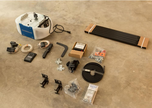
Let’s start with Hardware. This is the physical, tangible “thing” that you are going to produce. In the case of the smart garage door opener, there is a motor, gears, a metal case and a clear plastic light cover. A three-prong power cord plugs into an outlet and connects to the power supply inside the opener. Cables and wires connect all the printed circuit boards (PCB) together. Each board has chips, connectors, heat-sinks and other components. There are nuts, bolts, grommets and fasteners holding everything together. All of this is “hardware”. You can see some of this in the picture below.These items can be put into sub-groups under hardware: Board Specification, Mechanical Specification and System Specification. Now let’s look at each of these in a little more detail.
System Specification
The System Specification is where the “custom-off-the-shelf” (COTS) or “third-party” pieces are called out. In this case, the power supply (for converting the 120V AC from the house receptacle into 5V DC in the opener), the cable harnesses (connect the AC/DC power supply to each board), the gears, the screws and fasteners.From this specification, a System Bill Of Materials (BOM) is created which lists every unique item: a description of what it is, the vendor, the vendor part number, an optional internal part number and a placement designator. The BOM is used by the purchasing department to buy the necessary amount of materials to build the unit, and by the manufacturing group to know how to assemble it. For some products there literally no items that would be included in this specification, and for other products this is the only specification when they are built completely using COTS. I budget 15 hours on average for developing this specification.
Mechanical Specification
The Mechanical Specification defines the brackets, the metal case that houses everything, the clear plastic light cover, etc.. This specification provides the detail drawings of each piece with all dimensions, holes, hole diameters, bend lines and stamp areas. The designer uses a CAD (Computer Aided Design) program to create all the documents. The CAD files are used by the metal and plastic fabricators to create the housing. The specification can be created fairly easily as the bulk of the work is in the actual CAD file creation. Figure on 3 hours for the specification; but the CAD work can take from a few hours to many 10’s of hours depending on what is being designed. For a garage door housing and brackets, 10 hours should be sufficient.The CAD files are sent to the fabricator who cuts, bends, stamps, drills and otherwise works on the metal to create what is on the drawings. Similarly, a product may use a 3-D Printing (an additive process) or a CNC milling-machine (a subtractive process) to create pieces of the product. Rapid prototype companies can provide quick turn-around of low volumes in 1 to 3 days, but creating mechanical pieces can often take 1 to 3 weeks.
Hardware Board Specification
The Board Specification, also referred to as the Hardware Specification, contains all of the information about the various modules, chips, resistors, capacitors, antennae, heat sinks and other electronics, interconnect and passive components on a board. If there are multiple boards in a design, then there would typically be a specification for each board. This specification has the basic characteristics and implementation details for each component, and is a very condensed summary of the data sheet. This document focuses on the electrical parameters and connectivity of the components.If you are not familiar with all the types of components available to you as a designer, there is a helpful 3-Volume Encyclopedia of Electronic Components that set includes key information on electronics parts for your projects—complete with photographs, schematics, and diagrams.
Once you understand the components, here is an excellent reference provides the essential information that every circuit designer needs to produce a working circuit, as well as information on how to make a design that is robust, tolerant to noise and temperature, and able to operate in the system for which it is intended. It looks at best practices, design guidelines, and engineering knowledge gained from years of experience, and includes practical, real-world considerations for components and printed circuit boards (PCBs) as well as their manufacturability, reliability, and cost:
Of particular importance is the pin-out (e.g., what each pin or connection of a device actual does) for the components. Also included is the power usage and timing information. It’s also useful to include the device sizes (e.g., width, length, height and weight) for reference. How each device is used and how it connects with other devices on the board is described in this document. As such, the board specification is used as the guidelines for the schematics.
This is a rather detailed document; It can take 40 hours to read through data sheets and determine how devices work together. In the case of our garage door opener example, how does the processor on the board control the motor to turn the gears which opens/closes the door? How does the door status get read from a sensor and sent to the communications chip? All of the signals travel on wires / board traces to the pins of chips and the designer has to determine which pins and wires are connected.
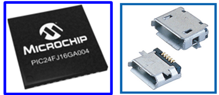
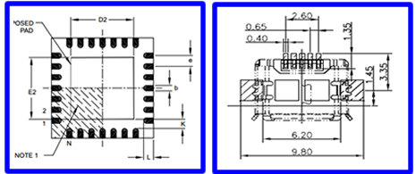
For an illustrative example of what occurs in the next stages let’s look at the PIC24FJ16GA004 microcontroller from Microchip, and a USB Micro-B connector from Assmann WSW Components. The microcontroller is an “active” component, where as the USB connector is a “passive” component.
This is what the actual components looks like (not to scale), and what would be soldered to the Printed Circuit Board (PCB):
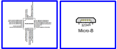
This is the pin-out diagram, which would be included in the Hardware Board Specification:
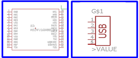
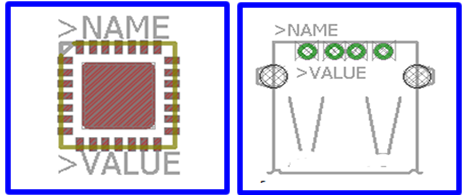
The schematic symbol created for the schematic library:
The physical dimensions of the device, along with the solder areas:
The layout symbol created for the PCB library:
You’ll need some tools to get started at this stage. The “Eagle” tools from Cadsoft (a division of Autodesk) are excellent for beginners, hobbyists, entrepreneurs as well as full scale industry engineering firms. The software scales from simple designs to very complex ones. Another tool vendor to consider is Altium. Most of the vendors have fully functional free version that are typically limited by either the number of components, the number of schematic pages, the physical board dimensions, number of board layers or some combination of all of these.
It’s also helpful to have a physical book to refer to as you are working with the these tools. The online materials available in .pdf format are extensive, but printing them can be costly and reading online can be straining.
Many schematic tools vendors include the most often used components in a packaged library, and vendors also have symbol libraries for their devices. However, there are many different schematic tools, and many different components; It is often the case that schematic symbols for major components in the design will need to be created. Once all the symbols are available, the engineer can connect the pins together as required for the design.
At this stage, all of the interconnects, passives, electromagnetic and active components for the design are accounted for on the schematic. The library for each of these contains a description, a vendor, a vendor part number and an optional internal part number. When a symbol is placed on the schematic, it is assigned a unique reference number which is used in the board assembly process. Once all of the parts are placed on the schematic, a parts Bill Of Materials (BOM) can be generated. This is used by the purchasing group to know how many of which item to buy.
Also, once all of the components have been connected or “wired” together on the schematic, a “netlist” can be created. This is a file which lists the network of connections between the components on the board and is used in creating the physical layout of the board.
This entire process is referred to the “Hardware Design” or “Schematic Capture”. For a small design with only a few components, budget about 15 hours for this step.
Depending on the selected components and their functionality, it may be possible to simulate the operational characteristics of the design. Many manufacturers provide simulation models for their components, and it is also possible to develop models “in-house” (or pay a third-party developer to create them). A first level simulation may only use simple static timing analysis (STA) models and generate cycle-based results. This is generally a less computationally intensive method to validate and verify basic operations .
For example, are address and data lines connected properly? Is combinatorial logic generating the expected output for a given input. At the other extreme, a fully simulated schematic will have parameters for all of the input buffer circuits, output driver circuits and internal times.
This timing parameters includes such things as:
Similar to the schematic capture library, there must e PCB library element for each component. Whereas the schematic symbol was a conceptual representation of the electrical connections of the component, the PCB symbol is an exact physical representation (width, length, height). The layout symbol shows the solder areas for the pins and pads for surface-mount parts, as well as where the holes are for through-hole components.
The PCB engineer places the components on the board and begins the process of placing metal traces to create the netlist connections indicated in the schematic. The “nets” in the schematic are virtual, abstracted connections, and the PCB connections are where the actual metal will be on the board. This is the stage where the ground (e.g., GND) and power (e.g., VCC or VDD) planes and connections are created.
The “writing” for the part outlines, component numbering, company name / logo, product information, etc. is put into a “silk screen” on either/both the top and bottom sides of the PCB.
PCB design is both a science and an art, especially for analog designs and high speed designs. For a simple, low-frequency, digital design the PCB layout can take at least as long as the schematic capture stage. In this example, would budget about 15 hours.
At the end of the board layout phase, the CAD software will generate a file to be used for the physical PCB creation. This file is commonly called a “Gerber” file. Each Gerber file represents only one PCB layer. That means you will usually get seven files for a two-layer board :
At a minimum, the physical connection netlist from the PCB layout should be compared to the netlist from the schematic capture. There should be a one-to-one correspondence between the two netlists. If they don’t match up, there is either a trace missing on the board, a trace added on the board or an incorrect trace routing on the board.
Simulations can become more accurate at this stage since the connections between components is defined. The characteristics of the connections depend on such things as the length, width and amount of material (e.g., the copper pour) used in the trace; The number of connections between different layers of the PCB (e.g., the vias), the dielectric / type of PCB material (e.g., FR4) and other factors.
It is also possible to simulate more than just the electrical signal characteristics of this virtual board. Heat maps and temperature profiles can be created; Electromagnetic interference (EMI) and electromagnetic radiation (EMR) – essentially how much “noise” does the system create at various frequencies – scans can be generated.
At this point, the actual design process is complete.
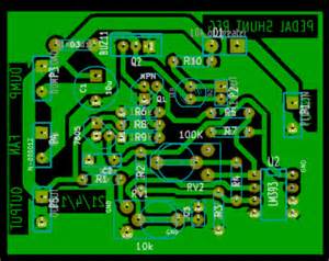
Here is an example of a “bare” board:

For reference, a small, 2-sided board with low number of components can be assembled in under 2 days for less than $50 per board. The cost drops significantly for a 1- to 2-week delivery. Per unit costs also decrease when ordered in volume, so the final production costs will considerably less than the initial prototype.
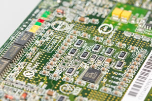
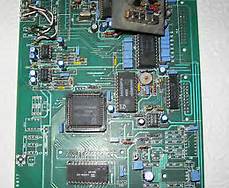
The final example, an assembled PCB:
This is what the actual components looks like (not to scale), and what would be soldered to the Printed Circuit Board (PCB):
This is the pin-out diagram, which would be included in the Hardware Board Specification:
The schematic symbol created for the schematic library:
The physical dimensions of the device, along with the solder areas:
The layout symbol created for the PCB library:
Hardware Design / Schematic Capture
With a comprehensive board specification and the relevant datasheets, a schematic can be created. The first step is to make a diagram or symbol for each component. These are also called “library elements”. This is a representation that shows the electrical connection for the device. This also has Power and Ground pins, which are often not shown on the schematic as these are common to many devices (the exception is when there are specific, non-common power and/or ground connections, often the case with communications or precision components).You’ll need some tools to get started at this stage. The “Eagle” tools from Cadsoft (a division of Autodesk) are excellent for beginners, hobbyists, entrepreneurs as well as full scale industry engineering firms. The software scales from simple designs to very complex ones. Another tool vendor to consider is Altium. Most of the vendors have fully functional free version that are typically limited by either the number of components, the number of schematic pages, the physical board dimensions, number of board layers or some combination of all of these.
It’s also helpful to have a physical book to refer to as you are working with the these tools. The online materials available in .pdf format are extensive, but printing them can be costly and reading online can be straining.
Many schematic tools vendors include the most often used components in a packaged library, and vendors also have symbol libraries for their devices. However, there are many different schematic tools, and many different components; It is often the case that schematic symbols for major components in the design will need to be created. Once all the symbols are available, the engineer can connect the pins together as required for the design.
At this stage, all of the interconnects, passives, electromagnetic and active components for the design are accounted for on the schematic. The library for each of these contains a description, a vendor, a vendor part number and an optional internal part number. When a symbol is placed on the schematic, it is assigned a unique reference number which is used in the board assembly process. Once all of the parts are placed on the schematic, a parts Bill Of Materials (BOM) can be generated. This is used by the purchasing group to know how many of which item to buy.
Also, once all of the components have been connected or “wired” together on the schematic, a “netlist” can be created. This is a file which lists the network of connections between the components on the board and is used in creating the physical layout of the board.
This entire process is referred to the “Hardware Design” or “Schematic Capture”. For a small design with only a few components, budget about 15 hours for this step.
Depending on the selected components and their functionality, it may be possible to simulate the operational characteristics of the design. Many manufacturers provide simulation models for their components, and it is also possible to develop models “in-house” (or pay a third-party developer to create them). A first level simulation may only use simple static timing analysis (STA) models and generate cycle-based results. This is generally a less computationally intensive method to validate and verify basic operations .
For example, are address and data lines connected properly? Is combinatorial logic generating the expected output for a given input. At the other extreme, a fully simulated schematic will have parameters for all of the input buffer circuits, output driver circuits and internal times.
This timing parameters includes such things as:
- Input Delay
- Output Delay
- Min/Max/Typical Input Skew
- Min/Max/Typical Output Skew
- Internal Propagation Delay
PCB Design / Board Layout
In the Printed Circuit Board (PCB) Design, also called “Board Layout”, stage the engineer determines how the physical board will look with all of the components in place. Using another software tool (although usually from the same vendor as the schematic capture tools), the designer creates a 2-dimensional shape of a board (e.g., a 3 inch x 5 inch rectangle or 4.5 inch diameter circle) to represent the PCB.Similar to the schematic capture library, there must e PCB library element for each component. Whereas the schematic symbol was a conceptual representation of the electrical connections of the component, the PCB symbol is an exact physical representation (width, length, height). The layout symbol shows the solder areas for the pins and pads for surface-mount parts, as well as where the holes are for through-hole components.
The PCB engineer places the components on the board and begins the process of placing metal traces to create the netlist connections indicated in the schematic. The “nets” in the schematic are virtual, abstracted connections, and the PCB connections are where the actual metal will be on the board. This is the stage where the ground (e.g., GND) and power (e.g., VCC or VDD) planes and connections are created.
The “writing” for the part outlines, component numbering, company name / logo, product information, etc. is put into a “silk screen” on either/both the top and bottom sides of the PCB.
PCB design is both a science and an art, especially for analog designs and high speed designs. For a simple, low-frequency, digital design the PCB layout can take at least as long as the schematic capture stage. In this example, would budget about 15 hours.
At the end of the board layout phase, the CAD software will generate a file to be used for the physical PCB creation. This file is commonly called a “Gerber” file. Each Gerber file represents only one PCB layer. That means you will usually get seven files for a two-layer board :
- Top layer
- Bottom layer
- Solder Stop Mask
- Solder Stop Mask
- Silk Top
- Silk Bottom
- Drill – some PCB fabricators may want a different format file named “excellon.cam”
At a minimum, the physical connection netlist from the PCB layout should be compared to the netlist from the schematic capture. There should be a one-to-one correspondence between the two netlists. If they don’t match up, there is either a trace missing on the board, a trace added on the board or an incorrect trace routing on the board.
Simulations can become more accurate at this stage since the connections between components is defined. The characteristics of the connections depend on such things as the length, width and amount of material (e.g., the copper pour) used in the trace; The number of connections between different layers of the PCB (e.g., the vias), the dielectric / type of PCB material (e.g., FR4) and other factors.
It is also possible to simulate more than just the electrical signal characteristics of this virtual board. Heat maps and temperature profiles can be created; Electromagnetic interference (EMI) and electromagnetic radiation (EMR) – essentially how much “noise” does the system create at various frequencies – scans can be generated.
At this point, the actual design process is complete.
PCB Fabrication
There are many places which will create the green (sometimes red) glass-reinforced epoxy laminate sheets that are the printed circuit board. A small, rectangular, 2-sided PCB can be produced very quickly for nominal cost. Many companies can quick-turn up to 10 PCBs in under 2 days for $25 to $50 each.Here is an example of a “bare” board:
Board Assembly /PCB Stuffing
With the components you ordered during the specification stage and the boards back from the fabricator, it’s time to “assemble” everything. Also called “stuffing” the board, this is where the parts are soldering to the board to create a finished product. Many designers will use the same company for fabrication and assembly. This can save on costs, since it’s a packaged price to include both services. And it can also save on time since there is no delay in mailing the PCB to you, and then you mailing the PCB plus components to the assembler.For reference, a small, 2-sided board with low number of components can be assembled in under 2 days for less than $50 per board. The cost drops significantly for a 1- to 2-week delivery. Per unit costs also decrease when ordered in volume, so the final production costs will considerably less than the initial prototype.
The final example, an assembled PCB:
The process for taking a concept through to a product starts with software to create a physical description for the various components, their placement and their connections. The output of the software program is used by the manufacturing / assembly house to make the PCB which is ready to accept the components.
There are many options available for PCB manufacturing, and these depend on your specific needs:
- Number of Boards (prototypes, development, pre-production, small production, large production)
- Turn-around time (overnight, days, 1-2 weeks)
- Price
- Component Type / Size
- Trace Widths
- Number of layers
- Number of Components
- Market (hobby, commercial, military, avionics, medical, etc.)
- Location (USA, China, Mexico)
A prototype is defined as ‘an original model on which something is patterned’.
A prototype circuit board is a working model of a printed circuit board (PCB) that has been created especially to check the functionality of the final PCB. A prototype can be created prior to a small as well as large-volume production requirement. In some cases, prototyping is also carried out for a single PCB requirement.
Why is a prototype needed?
Just as a circuit diagram of a PCB cannot serve as an effective base for manufacturing of the final product, it is imperative to first turn the diagram into an actual PCB and check its feasibility. Once the feasibility has been established and improvements have been analyzed, the actual working model can be manufactured.
There are several advantages to making prototype circuit boards::
- Once a prototype has been manufactured and tested, there are very few hurdles in the actual PCB manufacturing process.
- With a prototype, the customer gets a clear idea of how their end product would function. Risks and weak points, if any, can be easily identified at an early stage.
- Once a product goes into production, making changes to the product becomes very costly and time consuming; especially when large volume production is involved. Typically, production doesn\’t begin until the prototype circuit board has been approved by the customer.
There are several different types of PCBs that can be prototyped before they are put into production. These include single or multi-layer PCBs, flex or rigid PCBs, PCBs with IMS insulated metal substrate, and PF Rogers PCB. Prototyping can also be carried out for Flexible printed circuits (FPCs) which are used in several different applications. There are different types of FPCs such as single-sided FPC, dual access FPC, double-sided FPC and multilayer FPC.
Most PCB manufacturers offer prototyping services.. They will likely provide customers with several packages from which they can choose. A few manufacturers also give add-on services such as electrical testing and standard tooling for free. Such firms should be preferred as these free services give added value.
It typically takes a couple of days to manufacture prototype circuit boards. Experts recommend choosing a firm that specializes in PCB manufacturing and has a proven track record in the field. Before finalizing a prototyping project, ask the firm to provide some samples or references of their previous projects. Many firms also provide services to tweak and improve your existing prototype circuit board for better results.
The Program Counter (PC) is a register structure that contains the address pointer value of the current instruction. Each cycle, the value at the pointer is read into the instruction decoder and the program counter is updated to point to the next instruction. For RISC computers updating the PC register is as simple as adding the machine word length (in bytes) to the PC. In a CISC machine, however, the length of the current instruction needs to be calculated, and that length value needs to be added to the PC.
Updating the PC
The PC can be updated by making the enable signal high. After each instruction cycle the PC needs to be updated to point to the next instruction in memory. It is important to know how the memory is arranged before constructing your PC update circuit.Harvard-based systems tend to store one machine word per memory location. This means that every cycle the PC needs to be incremented by 1. Computers that share data and instruction memory together typically are byte addressable, which is to say that each byte has its own address, as opposed to each machine word having its own address. In these situations, the PC needs to be incremented by the number of bytes in the machine word.

Example: MIPS
The MIPS architecture uses a byte-addressable instruction memory unit. MIPS is a RISC computer, and that means that all the instructions are the same length: 32-bits. Every cycle, therefore, the PC needs to be incremented by 4 (32 bits = 4 bytes).
The MIPS architecture uses a byte-addressable instruction memory unit. MIPS is a RISC computer, and that means that all the instructions are the same length: 32-bits. Every cycle, therefore, the PC needs to be incremented by 4 (32 bits = 4 bytes).
Example: Intel IA32
The Intel IA32 (better known by some as "x86") is a CISC architecture, which means that each instruction can be a different length. The Intel memory is byte-addressable. Each cycle the instruction decoder needs to determine the length of the instruction, in bytes, and it needs to output that value to the PC. The PC unit increments itself by the value received from the instruction decoder.
The Intel IA32 (better known by some as "x86") is a CISC architecture, which means that each instruction can be a different length. The Intel memory is byte-addressable. Each cycle the instruction decoder needs to determine the length of the instruction, in bytes, and it needs to output that value to the PC. The PC unit increments itself by the value received from the instruction decoder.
Branching
Branching occurs at one of a set of special instructions known collectively as "branch" or "jump" instructions. In a branch or a jump, control is moved to a different instruction at a different location in instruction memory.During a branch, a new address for the PC is loaded, typically from the instruction or from a register. This new value is loaded into the PC, and future instructions are loaded from that location.
Non-Offset Branching
A non-offset branch, frequently referred to as a "jump" is a branch where the previous PC value is discarded and a new PC value is loaded from an external source.
Offset Branching
An offset branch is a branch where a value is added (or subtracted) to the current PC value to produce the new value. This is typically used in systems where the PC value is larger then a register value or an immediate value, and it is not possible to load a complete value into the PC. It is also commonly used to support relocatable binaries which may be loaded at an arbitrary base address.

Offset and Non-Offset Branching
Many systems have capabilities to use both offset and non-offset branching. Some systems may differentiate between the two as "near jump" and "far jump" respectively, although this terminology is archaic.
Program counter
The program counter (PC), commonly called the instruction pointer (IP) in Intel x86 and Itanium microprocessors, and sometimes called the instruction address register (IAR), the instruction counter, or just part of the instruction sequencer, is a processor register that indicates where a computer is in its program sequence.
In most processors, the PC is incremented after fetching an instruction, and holds the memory address of ("points to") the next instruction that would be executed. (In a processor where the incrementation precedes the fetch, the PC points to the current instruction being executed.)
Processors usually fetch instructions sequentially from memory, but control transfer instructions change the sequence by placing a new value in the PC. These include branches (sometimes called jumps), subroutine calls, and returns. A transfer that is conditional on the truth of some assertion lets the computer follow a different sequence under different conditions.
A branch provides that the next instruction is fetched from somewhere else in memory. A subroutine call not only branches but saves the preceding contents of the PC somewhere. A return retrieves the saved contents of the PC and places it back in the PC, resuming sequential execution with the instruction following the subroutine call.

Front panel of an IBM 701 computer introduced in 1952. Lights in the middle display the contents of various registers. The instruction counter is at the lower left.
Hardware implementation
In a typical central processing unit (CPU), the PC is a digital counter (which is the origin of the term "program counter") that may be one of many registers in the CPU hardware. The instruction cycle[4] begins with a fetch, in which the CPU places the value of the PC on the address bus to send it to the memory. The memory responds by sending the contents of that memory location on the data bus. (This is the stored-program computer model, in which executable instructions are stored alongside ordinary data in memory, and handled identically by it[5]). Following the fetch, the CPU proceeds to execution, taking some action based on the memory contents that it obtained. At some point in this cycle, the PC will be modified so that the next instruction executed is a different one (typically, incremented so that the next instruction is the one starting at the memory address immediately following the last memory location of the current instruction).Like other processor registers, the PC may be a bank of binary latches, each one representing one bit of the value of the PC.[6] The number of bits (the width of the PC) relates to the processor architecture. For instance, a “32-bit” CPU may use 32 bits to be able to address 232 units of memory. If the PC is a binary counter, it may increment when a pulse is applied to its COUNT UP input, or the CPU may compute some other value and load it into the PC by a pulse to its LOAD input.[7]
To identify the current instruction, the PC may be combined with other registers that identify a segment or page. This approach permits a PC with fewer bits by assuming that most memory units of interest are within the current vicinity.
Consequences in machine architecture
Use of a PC that normally increments assumes that what a computer does is execute a usually linear sequence of instructions. Such a PC is central to the von Neumann architecture. Thus programmers write a sequential control flow even for algorithms that do not have to be sequential. The resulting “von Neumann bottleneck” led to research into parallel computing, including non-von Neumann or dataflow models that did not use a PC; for example, rather than specifying sequential steps, the high-level programmer might specify desired function and the low-level programmer might specify this using combinatory logic.This research also led to ways to making conventional, PC-based, CPUs run faster, including:
- Pipelining, in which different hardware in the CPU executes different phases of multiple instructions simultaneously.
- The very long instruction word (VLIW) architecture, where a single instruction can achieve multiple effects.
- Techniques to predict out-of-order execution and prepare subsequent instructions for execution outside the regular sequence.
Consequences in high-level programming
Modern high-level programming languages still follow the sequential-execution model and, indeed, a common way of identifying programming errors is with a “procedure execution” in which the programmer's finger identifies the point of execution as a PC would. The high-level language is essentially the machine language of a virtual machine, too complex to be built as hardware but instead emulated or interpreted by software.However, new programming models transcend sequential-execution programming:
- When writing a multi-threaded program, the programmer may write each thread as a sequence of instructions without specifying the timing of any instruction relative to instructions in other threads.
- In event-driven programming, the programmer may write sequences of instructions to respond to events without specifying an overall sequence for the program.
- In dataflow programming, the programmer may write each section of a computing pipeline without specifying the timing relative to other sections.

Typical use of CR3 in address translation with 4 KiB pages
program counter is a register in a computer processor that contains the address (location) of the instruction being executed at the current time. As each instruction gets fetched, the program counter increases its stored value by 1.
Program counter(PC) , also called instruction pointer .
A branch provides that the next instruction is fetched from somewhere else in memory. A subroutine call not only branches but saves the preceding contents of the PC somewhere. A return retrieves the saved contents of the PC and places it back in the PC, resuming sequential execution with the instruction following the subroutine call.
A program counter is also known as an instruction counter, instruction pointer, instruction address register or sequence control register.
we will need both always. The program counter (PC) holds the address of the next instruction to be executed, while the instruction register (IR) holds the encoded instruction. Upon fetching the instruction, the program counter is incremented by one "address value" (to the location of the next instruction). The instruction is then decoded and executed appropriately.
The reason why you need both is because if you only had a program counter and used it for both purposes you would get the following troublesome system:
[Beginning of program execution]
- PC contains 0x00000000 (say this is start address of program in memory)
- Encoded instruction is fetched from the memory and placed into PC.
- The instruction is decoded and executed.
- Now it is time to move onto the next instruction so we go back to the PC to see what the address of the next instruction is. However, we have a problem because PC's previous address was removed so we have no idea where the next instruction is.
P.S. the width of the registers varies depending on the architecture's word size. For example, for a 32-bit processor, the word size is 32-bits. Therefore, the registers on the CPU would be 32 bits. Instruction registers are no different in dimensions. The difference is in the behavior and interpretation. Instructions are encoded in various forms, however, they still occupy a 32-bit register. For example, the Nios II processor from Altera contains 3 different instruction types, each encoded differently.
the Program Counter
What is the program counter?
The Program Counter (PC) is a register that is apart of all central processing unit (CPU) or microprocessor. All microcontrollers contains a microprocessor and thus has a program counter. The purpose of the program counter is to hold/store the address of the next instruction to be executed by the microcontroller's microprocessor.The size (width) of the program counter of a microcontroller is measured in bits and is directly related to the size of the microcontroller's program memory.
Determining the size of the AVR Program Counter
As mentioned above the purpose of the program counter (PC) is to hold the address of the next instruction to be executed by the CPU. Instructions are stores in the program memory of a microcontroller and thus the PC width is directly related to the size of the micorcontroller program memory. As an example lets determine the width of the program counter for the ATMega16 and ATMega32 AVR microcontrollers.
The width(size) of the program counter (PC) is basically the smallest possibly number of bits necessary to address the microcontroller program memory based on its organisation. Lets say n is the width of the PC then n would be related to the size of the program memory by the following equation:
2n = size of program memory
n = log(size of program memory)/(log2)
For the ATMega8515 microcontroller the program memory is 8k-Bytes organised as 4k-Words. As such the width of the ATMega8515 microcontroller Program Counter n is given by:
2n = 4k = 4x1024
n = log(4096)/log(2) = 12bits
For the ATMega16 microcontroller the program memory is 16k-Bytes organised as 8k-Words. As such the width of the ATMega16 microcontroller Program Counter n is given by:
2n = 8k = 8x1024
n = log(8192)/log(2) = 13bits
THE PROGRAM COUNTER AND ROM SPACE IN THE 8051
the role of the program counter (PC) register in executing an 8051 program. We also discuss ROM memory space for various 8051 family members.
Program counter in the 8051
Another important register in the 8051 is the PC (program counter). The program counter points to the address of the next instruction to be executed. As the CPU fetches the opcode from the program ROM, the program counter is incremented to point to the next instruction. The program counter in the 8051 is 16 bits wide. This means that the 8051 can access program addresses 0000 to FFFFH, a total of 64K bytes of code. However, not all members of the 8051 have the entire 64K bytes of on-chip ROM installed, as we will see soon. Where does the 8051 wake up when it is powered? We will discuss this important topic next.
Where the 8051 wakes up when it is powered up
One question that we must ask about any microcontroller (or microprocessor) is: At what address does the CPU wake up upon applying power to it? Each microprocessor is different. In the case of the 8051 family (that is, all members regardless of the maker and variation), the microcontroller wakes up at memory address 0000 when it is powered up. By powering up we mean applying Vcc to the RESET pin as discussed in Chapter 4. In other words, when the 8051 is powered up,.the PC (program counter) has the value of 0000 in it. This means that it expects the first opcode to be stored at ROM address OOOOH. For this reason in the 8051 system, the first opcode must be burned into memory location OOOOH of program ROM since this is where it looks for the first instruction when it is booted. We achieve this by the ORG statement in the source program as shown earlier. Next, we discuss the step-by-step action of the program counter in fetching and executing a sample program.
Placing code in program ROM
To get a better understanding of the role of the program counter in fetching and executing a program, we examine the action of the program counter as each instruction is fetched and executed. First, we examine once more the list file
of the sample program and how the code is placed in the ROM of an 8051 chip. As we can see, the opcode and operand for each instruction are listed on the left side of the list file.

Program21:ListFile

ROM Address
After the prografn is burned into ROM of an 8051 family member such as 8751 or AT8951 or DS5000, the opcode and operand are placed in ROM memory locations starting at 0000 as shown in the list below.

The list shows that address 0000 contains 7D, which is the opcode for moving a value into register R5, and address 0001 contains the operand (in this case 25H) to be moved to R5. Therefore, the instruction “MOV R5,#25H” has a machine code of “7D25″, where 7D is the opcode and 25 is the operand. Similarly, the machine code “7F34″ is located in memory locations 0002 and 0003 and represents the opcode and the operand for the instruction “MOV R7,#34H”. In the same way, machine code “7400″ is located in memory locations 0004 and 0005 and represents the opcode and the operand for the instruction “MOV A, #0″. The memory location 0006 has the opcode of 2D, which is the opcode for the
instruction “ADD A, R5″ and memory location 0007 has the content 2F, which is the opcode for the “ADD A, R7″ instruction. The opcode for the instruction “ADD A, #12H” is located at address 0008 and the operand 12H at address 0009. The memory location OOOA has the opcode for the SJMP instruction and its target address is located in location OOOB. The reason the target address is FE is explained in the next chapter.
Executing a program byte by byte
Assuming that the above program is burned into the ROM of an 8051 chip (or 8751, AT8951, or DS5000), the following is a step-by-step description of the action of the 8051 upon applying power to it.
- When the 8051 is powered up, the PC (program counter) has 0000 and starts
to fetch the first opcode from location 0000 of the program ROM. In the case
of the above program the first opcode is 7D, which is the code for moving an
operand to R5. Upon executing the opcode, the CPU fetches the value 25 and
places it in R5. Now one instruction is finished. Then the program counter is
incremented to point to 0002 (PC = 0002), which contains opcode 7F, the
opcode for the instruction “MOV R7 , . .”. - Upon executing the opcode 7F, the value 34H is moved into R7. Then the pro
gram counter is incremented to 0004. - ROM location 0004 has the opcode for the instruction “MOV A, #0″. This
instruction is executed and now PC = 0006. Notice that all the above instruc
tions are 2-byte instructions; that is, each one takes two memory locations. - Now PC = 0006 points to the next instruction, which is “ADD A, R5″. This is
a 1-byte instruction. After the execution of this instruction, PC = 0007. - The location 0007 has the opcode 2F, which belongs to the instruction “ADD
A,R7″. This also is a 1-byte instruction. Upon execution of this instruction,
PC is incremented to 0008. This process goes on until all the instructions are
fetched and executed. The fact that the program counter points at the next
instruction to be executed explains why some microprocessors (notably the
x86) call the program counter the instruction pointer.
ROM memory map in the 8051 family
As we saw in the last chapter, some family members have only 4K bytes of on-chip ROM (e.g., 8751, AT8951) and some, such as the AT89C52, have 8K bytes of ROM. Dallas Semiconductor’s DS5000-32 has 32K bytes of on-chip ROM. Dallas Semiconductor also has an 8051 with 64K bytes of on-chip ROM. The point to remember is that no member of the 8051 family can access more than 64K bytes of opcode since the program counter in the 8051 is a 16-bit register (0000 to FFFF address range). It must be noted that while the first location of program ROM inside the 8051 has the address of 0000, the last location can be different depending on the size of the ROM on the chip. Among the 8051 family members, the 8751 and AT8951 have 4K bytes of on-chip ROM. This 4K bytes of ROM memory has memory addresses of 0000 to OFFFH. Therefore, the first location of on-chip ROM of this 8051 has an address of 0000 and the last location has the address of OFFFH. Look at Example 2-1 to see how this is computed.
Example 2-1
Find the ROM memory address of each of the following 8051 chips.
(a) AT89C51 with 4KB (b) DS89C420 with 16KB (c) DS5000-32 with 32KB
Solution:

Figure 2-3. 8051 On-Chip ROM Address Range
(a) With 4K bytes of on-chip ROM memory space, we have 4096 bytes (4 x 1024 = 4096). This maps to address locations of 0000 to OFFFH. Notice that 0 is always the first location, (b) With 16K bytes of on-chip ROM memory space, we have 16,384 bytes (16 x 1024 = 16,384), which gives 0000 – 3FFFH. (c) With 32K bytes we have 32,768 bytes (32 x 1024 = 32,768). Converting 32,768 to hex, we get 8000H; therefore, the memory space is 0000 to 7FFFH.
8051 data type and directives
The 8051 microcontroller has only one data type. It is 8 bits, and the size of each register is also 8 bits. It is the job of the programmer to break down data larger than 8 bits (00 to FFH, or 0 to 255 in decimal) to be processed by the CPU. For examples of how to process data larger than 8 bits, see Chapter 6. The data types used by the 8051 can be positive or negative. A discussion of signed numbers is given in Chapter 6.
DB (define byte)
The DB directive is the most widely used data directive in the assembler. It is used to define the 8-bit data. When DB is used to define data, the numbers can be in decimal, binary, hex, or ASCII formats. For decimal, the “D” after the decimal number is optional, but using “B” (binary) and “H” (hexadecimal) for the others is required. Regardless of which is used, the assembler will convert the numbers into hex. To indicate ASCII, simply place the characters in quotation marks (‘like this’). The assembler will assign the ASCII code for the numbers or characters automatically. The DB directive is the only directive that can be used to define ASCII strings larger than two characters; therefore, it should be used for all ASCII data definitions. Following are some DB examples:

Either single or double quotes can be used around ASCII strings. This can be useful for strings, which contain a single quote such as “O’Leary”. DB is also used to allocate memory in byte-sized chunks.
Assembler directives
The following are some more widely used directives of the 8051.
ORG (origin)
The ORG directive is used to indicate the beginning of the address. The number that comes after ORG can be either in hex or in decimal. If the number is not followed by H, it is decimal and the assembler will convert it to hex. Some assemblers use “. ORG” (notice the dot) instead of “ORG” for the origin directive. Check your assembler.
EQU (equate)
This is used to define a constant without occupying a memory location. The EQU directive does not set aside storage for a data item but associates a constant value with a data label so that when the label appears in the program, itp constant value will be substituted for the label. The following uses EQU for the counter constant and then the constant is used to load the R3 register.

When executing the instruction “MOV R3, ttCOUNT”, the register R3 will be loaded with the value 25 (notice the # sign). What is the advantage of using EQU? Assume that there is a constant (a fixed value) used in many different places in the program, and the programmer wants to change its value throughout. By the use of EQU, the programmer can change it once and the assembler will change* all of its occurrences, rather than search the entire program trying to find every occurrence.
END directive
Another important pseudocode is the END directive. This indicates to the assembler the end of the source (asm) file. The END directive is the last line of an 8051 program, meaning that in the source code anything after the END directive is ignored by the assembler. Some assemblers use “. END” (notice the dot) instead
of “END”.
Rules for labels in Assembly language
By choosing label names that are meaningful, a programmer can make a program much easier to read and maintain. There are several rules that names must follow. First, each label name must be unique. The names used for labels in Assembly language programming consist of alphabetic letters in both uppercase and lowercase, the digits 0 through 9, and the special characters question mark (?), period (.), at (@), underline (_), and dollar sign ($). The first character of the label must be an alphabetic character. In other words it cannot be a number. Every assembler has some reserved words that must not be used as labels in the program. Foremost among the reserved words are the mnemonics for the instructions. For example, “MOV” and “ADD” are reserved since they are instruction mnemonics. In addition to the mnemonics there are some other reserved words
we look at the inside of the 8051. We demonstrate some of the widely used registers of the 8051 with simple instructions such as MOV and ADD. In Section 2.2 we examine. Assembly language and machine language programming and define terms such as mnemonics, opcode, operand, etc. The process of assembling and creating a ready-to-run program for the 8051 is discussed in Section 2.3. Step-by-step execution of an 8051 program and the role of the program counter are examined in Section 2.4. In Section 2.5 we look at some widely used Assembly language directives, pseudocode, and data types related to the 8051. In Section 2.6 we discuss the flag bits and how they are affected by arithmetic instructions. Allocation of RAM memory inside the 8051 plus the stack and register banks of the 8051 are discussed in Section 2.7.
SECTION 2.1: INSIDE THE 8051
In this section we examine the major registers of the 8051 and show their use with the simple instructions MOV and ADD.
Registers

In the CPU, registers are used to store
information temporarily. That information could be a byte of data to be processed, or an address pointing to the data to be fetched. The vast majority of 8051 registers are 8-bit registers. In the 8051 there is only one data type: 8 bits. The 8 bits of a register are shown in the diagram from the MSB (most significant bit) D7 to the LSB (least significant bit) DO. With an 8-bit data type, any data larger than 8 bits must be broken into 8-bit chunks before it is processed. Since there are a large number of registers in the 8051, we will concentrate on some of the widely used general-purpose registers and cover special registers in future chapters. See
Appendix A.2 for a complete list of 8051 registers.

Figure 2-1 (a). Some 8-bit Registers of the 8051

Figure 2-1 (b). Some 8051 16-bit Registers
The most widely used registers of the 8051 are A (accumulator), B, RO, Rl, R2, R3, R4, R5, R6, R7, DPTR (data pointer), and PC (program counter). All of the above registers are 8-bits, except DPTR and the program counter. The accumulator, register A, is used for all arithmetic and logic instructions. To understand the use of these registers, we will show them in the context of two simple instructions, MOV and ADD.
MOV instruction
Simply stated, the MOV instruction copies data from one location to another. It has the following format:
MOV destination,source ;copy source to dest.
This instruction tells the CPU to move (in reality, copy) the source operand to the destination operand. For example, the instruction “MOV A, RO” copies the contents of register RO to register A. After this instruction is executed, register A will have the same value as register RO. The MOV instruction does not affect the source operand. The following program first loads register A with value 55H (that is 55 in hex), then moves this value around to various registers inside the CPU. Notice the “#” in the instruction. This signifies that it is a value. The importance of this will be discussed soon.
MOV A,#55H ;load value 55H into reg. A
MOV RO,A ;copy contents of A into RO
;(now A=RO=55H)
MOV R1,A ,-copy contents of A into Rl
;(now A=RO=R1=55H)
MOV R2,A ;copy contents of A into R2
;now A=RO=R1=R2=55H)
MOV R3,#95H ;load value 95H into R3
;(now R3=95H)
MOV A,R3 /copy contents of R3 into A
;now A=R3=95H)
When programming the 8051 microcontroller, the following points should be noted: 1. Values can be loaded directly into any of registers A, B, or RO – R7. However,
to indicate that it is an immediate value it must be preceded with a pound sign
(#). This is shown next.
MOV A,#23H ;load 23H into A (A=23H)
MOV RO,#12H ;load 12H into RO (RO=12H)
MOV R1,#1FH ;load 1FH into Rl (R1=1FH)
MOV R2,#2BH ;load 2BH into R2 (R2=2BH)
MOV B,#3CH ;load 3CH into B (B=3CH)
MOV R7,#9DH ;load 9DH into R7 (R7=9DH)
MOV R5,#OF9H ;load F9H into R5 (R5=F9H)
MOV R6,#12 ,-load 12 decimal (OCH)
,-into reg. R6 (R6 = OCH)
Notice in instruction “MOV R5 , #0F9H” that a 0 is used between the # and F to indicate that F is a hex number and not a letter. In other words “MOV R5 , #F9H” will cause an error.- If values 0 to F are moved into an 8-bit register, the rest of the bits are assumed
to be all zeros. For example, in “MOV A, #5″ the result will be A = 05; that
is, A = 00000101 in binary.
- Moving a value that is too large into a register will cause an error.MOV A,#7F2H ;ILLEGAL: 7F2H > 8 bits (FFH) MOV R2,#456 ;ILLEGAL: 456 > 255 decimal (FFH)4. A value to be loaded into a register must be preceded with a pound sign (#).
Otherwise it means to load from a memory location. For example “MOV
A, 17H” means to move into A the value held in memory location 17H, which
could have any value. In order to load the value 17H into the accumulator we
must write “MOV A, #17H” with the # preceding the number. Notice that the
absence of the pound sign will not cause an error by the assembler since it is a
valid instruction. However, the result would not be what the programmer
intended. This is a common error for beginning programmers in the 8051.
ADD instruction
The ADD instruction has the following format:
ADD A,source ;ADD the source operand
;to the accumulator
The ADD instruction tells the CPU to add the source byte to register A and put the result in register A. To add two numbers such as 25H and 34H, each can be moved to a register and then added together:
MOV A,#25H /load 25H into A MOV R2,#34H ;load 34H into R2 ADD A,R2 /add R2 to accumulator
; (A = A + R2)
Executing the. program above results in A – 59H (25H + 34H = 59H) and R2 = 34H. Notice that the content of R2 does not change. The program above can be written in many ways, depending on the registers used. Another way might be:
MOV R5,#25H ;load 25H into R5 (R5=25H) MOV R7,#34H ;load 34H into R7 (R7=34H) MOV A,#0 /load 0 into A (A=0,clear A) ADD A,R5 ;add to A content of R5
; where A = A + R5 ADD A,R7 /add to A content of R7
; where A = A + R7
The program above results in A = 59H. There are always many ways to write the same program. One question that might come to mind after looking at the program above, is whether it is necessary to move both data items into registers before adding them together. The answer is no, it is not necessary. Look at the following variation of the same program:
MOV A,#25H ;load one operand into A (A=25H)
ADD A,#34H ;add the second operand 34H to A
In the above case, while one register contained one value, the second value followed the instruction as an operand. This is called an immediate operand. The examples shown so far for the ADD instruction indicate that the source operand can be either a register or immediate data, but the destination must always be register A, the accumulator. In other words, an instruction such as “ADD R2 , #12H” is invalid since register A (accumulator) must be involved in any arithmetic operation. Notice that “ADD R4, A” is also invalid for the reason that A must be the destination of any arithmetic operation. To put it simply: In the 8051, register A must be involved and be the destination for all arithmetic operations. The foregoing discussion explains why register A is referred to as the accumulator. The format for Assembly language instructions, descriptions of their use, and a listing of legal operand types are provided in Appendix A. 1.
There are two 16-bit registers in the 8051: PC (program counter) and DPTR (data pointer).
THE 8051 FAMILY
In this section we first look at the various members of the 8051 family of microcontrollers and their internal features. Plus we see who are the different manufacturers of the 8051 and what kind of products they offer.
A brief history of the 8051
In 1981, Intel Corporation introduced an 8-bit microcontroller called the 8051. This microcontroller had 128 bytes of RAM, 4K bytes of on-chip ROM, two timers, one serial port, and four ports (each 8-bits wide) all on a single chip. At the time it was also referred to as a “system on a chip.” The 8051 is an 8-bit processor, meaning that the CPU can work on only 8 bits of data at a time. Data larger than 8 bits has to be broken into 8-bit pieces to be processed by the CPU. The 8051 has a total of four I/O ports, each 8 bits wide. See Figure 1-2. Although the 8051 can have a maximum of 64K bytes of on-chip ROM, many manufacturers have put only 4K bytes on the chip. This will be discussed in more detail later.
Features of the 8051
The 8051 became widely popular after Intel allowed other manufacturers to make and market any flavors of the 8051 they please with the condition that they remain code-compatible with the 8051. This has led to many, versions of the 8051 with different speeds and amounts of on-chip ROM marketed by more than half a dozen manufacturers. Next we review some of them. It is important to note that although there are different flavors of the 8051 in terms of speed and amount of on-chip ROM, they are all compatible with the original 8051 as far as the instructions are concerned. This means that if you write your program for one, it will run on any of them regardless of the manufacturer.
8051 microcontroller
The 8051 is the original member of the 8051 family. Intel refers to it as MCS-51. Table 1-3 shows the main features of the 8051.
Figure 1-2. Inside the 8051 Microcontroller Block Diagram
Other members of the 8051 family
There are two other members in the 8051 family of microcontrollers. They are the 8052 and the 8031.
8052 microcontroller
The 8052 is another member of the 8051 family. The 8052 has all the standard features of the 8051 as well as an extra 128 bytes of RAM and an extra timer. In other words, the 8052 has 256 bytes of RAM and 3 timers. It also has 8K bytes of on-chip program ROM instead of 4K bytes. See Table 1 -4.
Table 1-4: Comparison of 8051 Family Members

8031 microcontroller
Another member of the 8051 family is the 8031 chip. This chip is often referred to as a ROM-less 8051 since it has OK bytes of on-chip ROM. To use this chip you must add external ROM to it. This external ROM must contain the program that the 8031 will fetch and execute. Contrast that to the 8051 in which the on-chip ROM contains the program to be fetched and executed but is limited to only 4K bytes of code. The ROM containing the program attached to the 8031 can be as large as 64K bytes. In the process of adding external ROM to the 8031, you lose two ports. That leaves only 2 ports (of the 4 ports) for I/O operations. To solve this problem, you can add external I/O to the 8031. Interfacing the 8031 with memory and I/O ports such as the 8255 chip is discussed in Chapter 14. There are also various speed versions of the 8031 available from different companies..
Various 8051 microcontrollers
Although the 8051 is the most popular member of the 8051 family, you will not see “8051″ in the part number. This is because the 8051 is available in different memory types, such as UV-EPROM, flash, and NV-RAM, all of which have different part numbers. A discussion of the various types of ROM will be given in Chapter 14. The UV-EPROM version of the 8051 is the 8751. The flash ROM version is marketed by many companies including Atmel Corp. and Dallas Semiconductor. The Atmel Flash 8051 is called AT89C51, while Dallas Semiconductor calls theirs DS89C4xO (DS89C420/430/440). The NV-RAM version of the 8051 made by Dallas Semiconductor is called DS5000. There is also an OTP (one-time programmable) version of the 8051 made by various manufacturers. Next we discuss briefly each of the above chips and describe applications where they are used.
8751 microcontroller
This 8751 chip has only 4K bytes of on-chip UV-EPROM. Using this chip for development requires access to a PROM burner, as well as a UV-EPROM eraser to erase the contents of UV-EPROM inside the 8751 chip before you can program it again. Because the on-chip ROM for the 8751 is UV-EPROM, it takes around 20 minutes to erase the 8751 before it can be programmed again. This has led many manufacturers to introduce flash and NV-RAM versions of the 8051, as we will discuss next. There are also various speed versions of the 8751 available from different companies.
DS89C4xO from Dallas Semiconductor (Maxim)
Many popular 8051 chips have on-chip ROM in the form of flash memory. The AT89C51 from Atmel Corp. is one example of an 8051 with flash ROM. This is ideal for fast development since flash memory can be erased in seconds compared to the twenty minutes or more needed for the 8751. For this reason the AT89C51 is used in place of the 8751 to eliminate the waiting time needed to erase the chip and thereby speed up the development time. Using the AT89C51 to develop a microcontroller-based system requires a ROM burner that supports flash memory; however, a ROM eraser is not needed. Notice that in flash memory you must erase the entire contents of ROM in order to program it again. This erasing of flash is done by the PROM burner itself, which is why a separate eraser is not needed. To eliminate the need for a PROM burner, Dallas Semiconductor, now part of the Maxim Corp., has a version of the 8051/52 called DS89C4xO (DS89C420/430/…) that can be programmed via the serial COM port of an IBM
PC-Notice that the on-chip ROM for the DS89C4xO is in the form of flash.
The DS89C4xO (420/430/440/450) comes with an on-chip loader, which allows the program to be loaded into the on-chip flash ROM while it is in the system. This can be done via the serial COM port of an IBM PC. This in-system program loading of the DS89C4xO via a PC serial COM port makes it an ideal home development system. Dallas Semiconductor also has an NV-RAM version of the 8051 called DS5000. The advantage of NV-RAM is the ability to change the ROM contents one byte at a time. The DS5000 also comes with a loader, allowing it to be programmed via the PC’s COM port. See Table 1-5. From Table 1-5, notice that the DS89C4xO is a really an 8052 chip since it has 256 bytes of RAM and 3 timers.

X
Source: www.maxim-ic.com/products/microcontrollers/805 l_drop_in.cfm
DS89C4xO Trainer
In Chapter 8, we discuss the design of DS89C4xO Trainer extensively. The MDE8051 Trainer is available from www.MicroDigitalEd.com. This Trainer allows you to program the DS89C4xO chip from the COM port of the x86 IBM PC, with no need for a ROM burner.
For a DS89C4xO-based trainer see www.MicroDigitalEd.com.
AT89C51 from Atmel Corporation
The Atmel Corp. has a wide selection of 8051 chips, as shown in Tables 1-6 and 1-7. For example, the AT89C51 is a popular and inexpensive chip used in many small projects. It has 4K bytes of flash ROM. Notice the AT89C51-12PC, where “C” before the 51 stands for CMOS, which has a low power consumption, “12″ indicates 12 MHz, “P” is for plastic DIP package, “C” is for commercial.
Table 1-6: Versions of 8051 From Atmel (All ROM Flash)

Note: “C” in the part number indicates CMOS.
Table 1-7: Various Speeds of 8051 From Atmel

OTP version of the 8051
There are also OTP (one-time-programmable) versions of the 8051 available from different sources. Flash and NV-RAM versions are typically used for product development. When a product is designed and absolutely finalized, the OTP version of the 8051 is used for mass production since it is much cheaper in terms of price per unit.
8051 family from Philips
Another major producer of the 8051 family is Philips Corporation. Indeed, they have one of the largest selections of 8051 microcontrollers. Many of their products include features such as A-to-D converters, D-to-A converters, extended I/O, and both OTP and flash
ASSEMBLING AND RUNNING AN 8051 PROGRAM
Now that the basic form of an Assembly language program has been given, the next question is: How it is created, assembled, and made ready to run? The steps to create an executable Assembly language program are outlined as follows.
- First we use an editor to type in a program similar to Program 2-1.Many excellent editors or word processors are available that can be used to create and/or edit the program. A widely used editor is the MS-DOS EDIT program (or Notepad in Windows), which comes with all Microsoft operating systems.Notice that the editor must be able to produce an ASCII file. For many assemblers, the file names follow the usual DOS conventions, but the source file has the extension “asm” or “src”, depending on which assembler you are using. Check your assembler for the convention. The “asm” extension for the source file is used by an assembler in the next step.
- The “asm” source file containing the program code created in step 1 is fed to an 8051 assembler. The assembler converts the instructions into

Figure 2-2. Steps to Create a Program
machine code. The assembler will produce an object file and a list file. The extension for the object file is “obj” while the extension for the list file is “1st”.
- Assemblers require a third step called linking. The link program takes one or
more object files and produces an absolute object file with the extension “abs”
This abs file is used by 8051 trainers that have a monitor program. - Next, the “abs” file is fed into a program called “OH” (object to hex convert
er), which creates a file with extension “hex” that is ready to burn into ROM.
This program comes with all 8051 assemblers. Recent Windows-based assem
blers combine steps 2 through 4 into one step.
More about “asm” and “obj” files
The “asm” file is also called the source file and for this reason some assemblers require that this file have the “src” extension. Check your 8051 assembler to see which extension it requires. As mentioned earlier, this file is created with an editor such as DOS EDIT or Windows Notepad. The 8051 assembler converts the asm file’s Assembly language instructions into machine language and provides the obj (object) file. In addition to creating the object file, the assembler also produces the 1st file (list file).
1st file
The 1st (list) file, which is optional, is very useful to the programmer because it lists all the opcodes and addresses as well as errors that the assembler detected. Many assemblers assume that the list file is not wanted unless you indicate that you want to produce it. This file can be accessed by an editor such as DOS EDIT and displayed on the monitor or sent to the printer to produce a hard copy. The programmer uses the list file to find syntax errors. It is only after fixing all the errors indicated in the 1st file that the obj file is ready to be input to the linker program.

8051 Microcontroller
A micro controller is an integrated circuit or a chip with a processor and other support devices like program memory, data memory, I/O ports, serial communication interface etc integrated together. Unlike a microprocessor (ex: Intel 8085), a microcontroller does not require any external interfacing of support devices. Intel 8051 is the most popular microcontroller ever produced in the world market. Now lets talk about 8051 microcontroller in detail.
Before going further, it will be interesting for you to understand the difference between a Microprocessor and Microcontroller. We have a detailed article which describes the basic difference between both.
Here is a Quick Access to various sections of this article:-
Pin Diagram :- Internal Architecture :- Program Memory Organization :- Data Memory Organization :-8051 System Clock :- 8051 Reset Circuit
Introduction
Intel first produced a microcontroller in 1976 under the name MCS-48, which was an 8 bit microcontroller. Later in 1980 they released a further improved version (which is also 8 bit), under the name MCS-51. The most popular microcontroller 8051 belongs to the MCS-51 family of microcontrollers by Intel. Following the success of 8051, many other semiconductor manufacturers released microcontrollers under their own brand name but using the MCS-51 core. Global companies and giants in semiconductor industry like Microchip, Zilog, Atmel, Philips, Siemens released products under their brand name. The specialty was that all these devices could be programmed using the same MCS-51 instruction sets. They basically differed in support device configurations like improved memory, presence of an ADC or DAC etc. Intel then released its first 16 bit microcontroller in 1982, under name MCS-96
Note:- Read the Story and History about Intel – the making of first Micro processor and more!
8051 Microcontroller Packaging
There is no need of explaining what each package means, you already know it. So I will skim through mainly used packaging for 8051. See, availability of various packages change from device to device. The most commonly used is Dual Inline Package (40 pins) – known popularly as DIP. 8051 is also available in QFP (Quad Flat Package), TQFP (Thin Quad Flat Package), PQFP (Plastic Quad Flat Package) etc. For explaining the pin diagram, we have used a 40 pin DIP IC as model.
8051 Microcontroller Architecture
Its possible to explain microcontroller architecture to a great detail, but we are limiting scope of this article to internal architecture, pin configuration, program memory and data memory organization. The basic architecture remains same for the MCS-51 family. In general all microcontrollers in MCS- 51 family are represented by XX51, where XX can take values like 80, 89 etc.
Schematic and Features

The general schematic diagram of 8051 microcontroller is shown above. We can see 3 system inputs, 3 control signals and 4 ports (for external interfacing). A Vcc power supply and ground is also shown. Now lets explain and go through each in detail. System inputs are necessary to make the micro controller functional. So the first and most important of this is power, marked as Vcc with a GND (ground potential). Without proper power supply, no electronic system would work. XTAL 1 and XTAL 2 are for the system clock inputs from crystal clock circuit. RESET input is required to initialize microcontroller to default/desired values and to make a new start.
There are 3 control signals, EA,PSEN and ALE. These signals known as External Access (EA), Program Store Enable (PSEN), and Address Latch Enable (ALE) are used for external memory interfacing.
Take a look at the schematic diagram below (a functional microcontroller)

As mentioned above, control signals are used for external memory interfacing. If there is no requirement of external memory interfacing then, EA pin is pulled high (connected to Vcc) and two others PSEN and ALE are left alone. You can also see a 0.1 micro farad decoupling capacitor connected to Vcc (to avoid HF oscillations at input).
There are four ports numbered 0,1,2,3 and called as Port 0, Port 1, Port 2 and Port 3 which are used for external interfacing of devices like DAC, ADC, 7 segment display, LED etc. Each port has 8 I/O lines and they all are bit programmable.
8051 Pin Diagram & Description

For describing pin diagram and pin configuration of 8051, we are taking into consideration a 40 pin DIP (Dual inline package). Now lets go through pin configuration in detail.
Pin-40 : Named as Vcc is the main power source. Usually its +5V DC.
You may note some pins are designated with two signals (shown in brackets).
Pins 32-39: Known as Port 0 (P0.0 to P0.7) – In addition to serving as I/O port, lower order address and data bus signals are multiplexed with this port (to serve the purpose of external memory interfacing). This is a bi directional I/O port (the only one in 8051) and external pull up resistors are required to function this port as I/O.
Pin-31:- ALE aka Address Latch Enable is used to demultiplex the address-data signal of port 0 (for external memory interfacing.) 2 ALE pulses are available for each machine cycle.
Pin-30:- EA/ External Access input is used to enable or disallow external memory interfacing. If there is no external memory requirement, this pin is pulled high by connecting it to Vcc.
Pin- 29:- PSEN or Program Store Enable is used to read signal from external program memory.
Pins- 21-28:- Known as Port 2 (P 2.0 to P 2.7) – in addition to serving as I/O port, higher order address bus signals are multiplexed with this quasi bi directional port.
Pin 20:- Named as Vss – it represents ground (0 V) connection.
Pins 18 and 19:- Used for interfacing an external crystal to provide system clock.
Pins 10 – 17:- Known as Port 3. This port also serves some other functions like interrupts, timer input, control signals for external memory interfacing RD and WR , serial communication signals RxD and TxD etc. This is a quasi bi directional port with internal pull up.
Pin 9:- As explained before RESET pin is used to set the 8051 microcontroller to its initial values, while the microcontroller is working or at the initial start of application. The RESET pin must be set high for 2 machine cycles.
Pins 1 – 8:- Known as Port 1. Unlike other ports, this port does not serve any other functions. Port 1 is an internally pulled up, quasi bi directional I/O port.
8051 Internal Architecture

There is no need of any detailed explanation to understand internal architecture of 8051 micro controller. Just look at the diagram above and you observer it carefully. The system bus connects all the support devices with the central processing unit. 8051 system bus composes of an 8 bit data bus and a 16 bit address bus and bus control signals. From the figure you can understand that all other devices like program memory, ports, data memory, serial interface, interrupt control, timers, and the central processing unit are all interfaced together through the system bus. RxD and TxD (serial port input and output) are interfaced with port 3.
8051 Memory Organization
Before going deep into the memory architecture of 8051, lets talk a little bit about two variations available for the same. They are Princeton architecture and Harvard architecture. Princeton architecture treats address memory and data memory as a single unit (does not distinguish between two) where as Harvard architecture treats program memory and data memory as separate entities. Thus Harvard architecture demands address, data and control bus for accessing them separately where as Princeton architecture does not demand any such separate bus.
Example:- 8051 micro controller is based on Harvard architecture and 8085 micro processor is based on Princeton architecture.
Thus 8051 has two memories :- Program memory and Data memory
Program memory organization

Now lets dive into the program memory organization 0f 8051. It has an internal program of 4K size and if needed an external memory can be added (by interfacing ) of size 60K maximum. So in total 64K size memory is available for 8051 micro controller. By default, the External Access (EA) pin should be connected Vcc so that instructions are fetched from internal memory initially. When the limit of internal memory (4K) is crossed, control will automatically move to external memory to fetch remaining instructions. If the programmer wants to fetch instruction from external memory only (bypassing the internal memory), then he must connect External Access (EA) pin to ground (GND).
You may already know that 8051 has a special feature of locking the program memory (internal) and hence protecting against software piracy. This feature is enable by program lock bits. Once these bits are programmed, contents of internal memory can not be accessed using an external circuitry. How ever locking the software is not possible if external memory is also used to store the software code. Only internal memory can be locked and protected. Once locked, these bits can be unlocked only by a memory-erase operation, which in turn will erase the programs in internal memory too.
8051 is capable of pipelining. Pipelining makes a processor capable of fetching the next instruction while executing previous instruction. Its some thing like multi tasking, doing more than one operation at a time. 8051 is capable of fetching first byte of the next instruction while executing the previous instruction.
Data memory organization

In the MCS-51 family, 8051 has 128 bytes of internal data memory and it allows interfacing external data memory of maximum size up to 64K. So the total size of data memory in 8051 can be upto 64K (external) + 128 bytes (internal). Observe the diagram carefully to get more understanding. So there are 3 separations/divisions of the data memory:- 1) Register banks 2) Bit addressable area 3) Scratch pad area.

Register banks form the lowest 32 bytes on internal memory and there are 4 register banks designated bank #0,#1, #2 and #3. Each bank has 8 registers which are designated as R0,R1…R7. At a time only one register bank is selected for operations and the registers inside the selected bank are accessed using mnemonics R0..R1.. etc. Other registers can be accessed simultaneously only by direct addressing. Registers are used to store data or operands during executions. By default register bank #0 is selected (after a system reset).
The bit addressable ares of 8051 is usually used to store bit variables. The bit addressable area is formed by the 16 bytes next to register banks. They are designated from address 20H to 2FH (total 128 bits). Each bits can be accessed from 00H to 7FH within this 128 bits from 20H to 2FH. Bit addressable area is mainly used to store bit variables from application program, like status of an output device like LED or Motor (ON/OFF) etc. We need only a bit to store this status and using a complete byte addressable area for storing this is really bad programming practice, since it results in wastage of memory.
The scratch pad area is the upper 80 bytes which is used for general purpose storage. Scratch pad area is from 30H to 7FH and this includes stack too.
8051 System Clock

An 8051 clock circuit is shown above. In general cases, a quartz crystal is used to make the clock circuit. The connection is shown in figure (a) and note the connections to XTAL 1 and XTAL 2. In some cases external clock sources are used and you can see the various connections above. Clock frequency limits (maximum and minimum) may change from device to device. Standard practice is to use 12MHz frequency. If serial communications are involved then its best to use 11.0592 MHz frequency.

Okay, take a look at the above machine cycle waveform. One complete oscillation of the clock source is called a pulse. Two pulses forms a state and six states forms one machine cycle. Also note that, two pulses of ALE are available for 1 machine cycle.
8051 Reset Circuit

8051 can be reset in two ways 1) is power-on reset – which resets the 8051 when power is turned ON and 2) manual reset – in which a reset happens only when a push button is pressed manually. Two different reset circuits are shown above. A reset doesn’t affect contents of internal RAM. For reset to happen, the reset input pin (pin 9) must be active high for atleast 2 machine cycles. During a reset operation :- Program counter is cleared and it starts from 00H, register bank #0 is selected as default, Stack pointer is initialized to 07H, all ports are written with FFH.
XXX . XXX 4%zero null 0 1 2 3 4 Hardware architecture
Hardware architecture
In engineering, hardware architecture refers to the identification of a system's physical components and their interrelationships. This description, often called a hardware design model, allows hardware designers to understand how their components fit into a system architecture and provides to software component designers important information needed for software development and integration. Clear definition of a hardware architecture allows the various traditional engineering disciplines (e.g., electrical and mechanical engineering) to work more effectively together to develop and manufacture new machines, devices and components.[1]
Hardware is also an expression used within the computer engineering industry to explicitly distinguish the (electronic computer) hardware from the software that runs on it. But hardware, within the automation and software engineering disciplines, need not simply be a computer of some sort. A modern automobile runs vastly more software than the Apollo spacecraft. Also, modern aircraft cannot function without running tens of millions of computer instructions embedded and distributed throughout the aircraft and resident in both standard computer hardware and in specialized hardward components such as IC wired logic gates, analog and hybrid devices, and other digital components. The need to effectively model how separate physical components combine to form complex systems is important over a wide range of applications, including computers, personal digital assistants (PDAs), cell phones, surgical instrumentation, satellites, and submarines.
Hardware architecture is the representation of an engineered (or to be engineered) electronic or electromechanical hardware system, and the process and discipline for effectively implementing the design(s) for such a system. It is generally part of a larger integrated system encompassing information, software, and device prototyping.[2]
It is a representation because it is used to convey information about the related elements comprising a hardware system, the relationships among those elements, and the rules governing those relationships.
It is a process because a sequence of steps is prescribed to produce or change the architecture, and/or a design from that architecture, of a hardware system within a set of constraints.
It is a discipline because a body of knowledge is used to inform practitioners as to the most effective way to design the system within a set of constraints.
A hardware architecture is primarily concerned with the internal electrical (and, more rarely, the mechanical) interfaces among the system's components or subsystems, and the interface between the system and its external environment, especially the devices operated by or the electronic displays viewed by a user. (This latter, special interface, is known as the computer human interface, AKA human computer interface, or HCI; formerly called the man-machine interface.)[3] Integrated circuit (IC) designers are driving current technologies into innovative approaches for new products. Hence, multiple layers of active devices are being proposed as single chip, opening up opportunities for disruptive microelectronic, optoelectronic, and new microelectromechanical hardware implementation.
Prior to the advent of digital computers, the electronics and other engineering disciplines used the terms system and hardware as they are still commonly used today. However, with the arrival of digital computers on the scene and the development of software engineering as a separate discipline, it was often necessary to distinguish among engineered hardware artifacts, software artifacts, and the combined artifacts.
A programmable hardware artifact, or machine, that lacks its computer program is impotent; even as a software artifact, or program, is equally impotent unless it can be used to alter the sequential states of a suitable (hardware) machine. However, a hardware machine and its programming can be designed to perform an almost illimitable number of abstract and physical tasks. Within the computer and software engineering disciplines (and, often, other engineering disciplines, such as communications), then, the terms hardware, software, and system came to distinguish between the hardware that runs a computer program, the software, and the hardware device complete with its program.
The hardware engineer or architect deals (more or less) exclusively with the hardware device; the software engineer or architect deals (more or less) exclusively with the program; and the systems engineer or systems architect is responsible for seeing that the programming is capable of properly running within the hardware device, and that the system composed of the two entities is capable of properly interacting with its external environment, especially the user, and performing its intended function.
A hardware architecture, then, is an abstract representation of an electronic or an electromechanical device capable of running a fixed or changeable program.
A hardware architecture generally includes some form of analog, digital, or hybrid electronic computer, along with electronic and mechanical sensors and actuators. Hardware design may be viewed as a 'partitioning scheme,' or algorithm, which considers all of the system's present and foreseeable requirements and arranges the necessary hardware components into a workable set of cleanly bounded subsystems with no more parts than are required. That is, it is a partitioning scheme that is exclusive, inclusive, and exhaustive. A major purpose of the partitioning is to arrange the elements in the hardware subsystems so that there is a minimum of electrical connections and electronic communications needed among them. In both software and hardware, a good subsystem tends to be seen as a meaningful "object." Moreover, a clear allocation of user requirements to the architecture (hardware and software) provides an effective basis for validation tests of the user's requirements in the as-built system


Hardware is also an expression used within the computer engineering industry to explicitly distinguish the (electronic computer) hardware from the software that runs on it. But hardware, within the automation and software engineering disciplines, need not simply be a computer of some sort. A modern automobile runs vastly more software than the Apollo spacecraft. Also, modern aircraft cannot function without running tens of millions of computer instructions embedded and distributed throughout the aircraft and resident in both standard computer hardware and in specialized hardward components such as IC wired logic gates, analog and hybrid devices, and other digital components. The need to effectively model how separate physical components combine to form complex systems is important over a wide range of applications, including computers, personal digital assistants (PDAs), cell phones, surgical instrumentation, satellites, and submarines.
Hardware architecture is the representation of an engineered (or to be engineered) electronic or electromechanical hardware system, and the process and discipline for effectively implementing the design(s) for such a system. It is generally part of a larger integrated system encompassing information, software, and device prototyping.[2]
It is a representation because it is used to convey information about the related elements comprising a hardware system, the relationships among those elements, and the rules governing those relationships.
It is a process because a sequence of steps is prescribed to produce or change the architecture, and/or a design from that architecture, of a hardware system within a set of constraints.

It is a discipline because a body of knowledge is used to inform practitioners as to the most effective way to design the system within a set of constraints.
A hardware architecture is primarily concerned with the internal electrical (and, more rarely, the mechanical) interfaces among the system's components or subsystems, and the interface between the system and its external environment, especially the devices operated by or the electronic displays viewed by a user. (This latter, special interface, is known as the computer human interface, AKA human computer interface, or HCI; formerly called the man-machine interface.)[3] Integrated circuit (IC) designers are driving current technologies into innovative approaches for new products. Hence, multiple layers of active devices are being proposed as single chip, opening up opportunities for disruptive microelectronic, optoelectronic, and new microelectromechanical hardware implementation.
Background


A programmable hardware artifact, or machine, that lacks its computer program is impotent; even as a software artifact, or program, is equally impotent unless it can be used to alter the sequential states of a suitable (hardware) machine. However, a hardware machine and its programming can be designed to perform an almost illimitable number of abstract and physical tasks. Within the computer and software engineering disciplines (and, often, other engineering disciplines, such as communications), then, the terms hardware, software, and system came to distinguish between the hardware that runs a computer program, the software, and the hardware device complete with its program.
The hardware engineer or architect deals (more or less) exclusively with the hardware device; the software engineer or architect deals (more or less) exclusively with the program; and the systems engineer or systems architect is responsible for seeing that the programming is capable of properly running within the hardware device, and that the system composed of the two entities is capable of properly interacting with its external environment, especially the user, and performing its intended function.
A hardware architecture, then, is an abstract representation of an electronic or an electromechanical device capable of running a fixed or changeable program.
A hardware architecture generally includes some form of analog, digital, or hybrid electronic computer, along with electronic and mechanical sensors and actuators. Hardware design may be viewed as a 'partitioning scheme,' or algorithm, which considers all of the system's present and foreseeable requirements and arranges the necessary hardware components into a workable set of cleanly bounded subsystems with no more parts than are required. That is, it is a partitioning scheme that is exclusive, inclusive, and exhaustive. A major purpose of the partitioning is to arrange the elements in the hardware subsystems so that there is a minimum of electrical connections and electronic communications needed among them. In both software and hardware, a good subsystem tends to be seen as a meaningful "object." Moreover, a clear allocation of user requirements to the architecture (hardware and software) provides an effective basis for validation tests of the user's requirements in the as-built system
The hardware systems architect or hardware architect is responsible for:
- Interfacing with a systems architect or client stakeholders. It is extraordinarily rare nowadays for sufficiently large and/or complex hardware systems that require a hardware architect not to require substantial software and a systems architect. The hardware architect will therefore normally interface with a systems architect, rather than directly with user(s), sponsor(s), or other client stakeholders. However, in the absence of a systems architect, the hardware systems architect must be prepared to interface directly with the client stakeholders in order to determine their (evolving) needs to be realized in hardware. The hardware architect may also need to interface directly with a software architect or engineer(s), or with other mechanical or electrical engineers.
- Generating the highest level of hardware requirements, based on the user's needs and other constraints such as cost and schedule.
- Ensuring that this set of high level requirements is consistent, complete, correct, and operationally defined.
- Performing cost–benefit analyses to determine the best methods or approaches for meeting the hardware requirements; making maximum use of commercial off-the-shelf or already developed components.
- Developing partitioning algorithms (and other processes) to allocate all present and foreseeable (hardware) requirements into discrete hardware partitions such that a minimum of communications is needed among partitions, and between the user and the system.
- Partitioning large hardware systems into (successive layers of) subsystems and components each of which can be handled by a single hardware engineer or team of engineers.
- Ensuring that maximally robust hardware architecture is developed.
- Generating a set of acceptance test requirements, together with the designers, test engineers, and the user, which determine that all of the high level hardware requirements have been met, especially for the computer-human-interface.
- Generating products such as sketches, models, an early user's manual, and prototypes to keep the user and the engineers constantly up to date and in agreement on the system to be provided as it is evolving
The user/sponsor should view the architect as the user's representative and provide all input through the architect. Direct interaction with project engineers is generally discouraged as the chance of mutual misunderstanding is very high. The user requirements' specification should be a joint product of the user and hardware architect (or, the systems and hardware architects): the user brings his needs and wish list, the architect brings knowledge of what is likely to prove doable within cost and time constraints. When the user needs are translated into a set of high level requirements is also the best time to write the first version of the acceptance test, which should, thereafter, be religiously kept up to date with the requirements. That way, the user will be absolutely clear about what s/he is getting. It is also a safeguard against untestable requirements, misunderstandings, and requirements creep.
The development of the first level of hardware engineering requirements is not a purely analytical exercise and should also involve both the hardware architect and engineer. If any compromises are to be made—to meet constraints like cost, schedule, power, or space, the architect must ensure that the final product and overall look and feel do not stray very far from the user's intent. The engineer should focus on developing a design that optimizes the constraints but ensures a workable and reliable product. The architect is primarily concerned with the comfort and usability of the product; the engineer is primarily concerned with the producibility and utility of the product.
The provision of needed services to the user is the true function of an engineered system. However, as systems become ever larger and more complex, and as their emphases move away from simple hardware components, the narrow application of traditional hardware development principles is found to be insufficient—the application of the more general principles of hardware architecture to the design of (sub) systems is seen to be needed. A Hardware architecture is also a simplified model of the finished end product—its primary function is to define the hardware components and their relationships to each other so that the whole can be seen to be a consistent, complete, and correct representation of what the user had in mind—especially for the computer–human interface. It is also used to ensure that the components fit together and relate in the desired way.
It is necessary to distinguish between the architecture of the user's world and the engineered hardware architecture. The former represents and addresses problems and solutions in the user's world. It is principally captured in the computer–human interfaces (CHI) of the engineered system. The engineered system represents the engineering solutions—how the engineer proposes to develop and/or select and combine the components of the technical infrastructure to support the CHI. In the absence of an architect, there is an unfortunate tendency to confuse the two architectures, since the engineer thinks in terms of hardware, but the user may be thinking in terms of solving a problem of getting people from point A to point B in a reasonable amount of time and with a reasonable expenditure of energy, or of getting needed information to customers and staff. A hardware architect is expected to combine knowledge of both the architecture of the user's world and of (all potentially useful) hardware engineering architectures. The former is a joint activity with the user; the latter is a joint activity with the engineers. The product is a set of high level requirements reflecting the user's requirements which can be used by the engineers to develop hardware systems design requirements.
Because requirements evolve over the course of a project, especially a long one, an architect is needed until the hardware system is accepted by the user: the architect is the best insurance that no changes and interpretations made during the course of development compromise the user's viewpoint.
+++++++++++++++++++++++++++++++++++++++++++++++++++++++++++++++++++++++
Design of electronic devices (Hardware design) = Performance of components and materials of electronics
+++++++++++++++++++++++++++++++++++++++++++++++++++++++++++++++++++++++
Given article is useful and informative.The article shared more informations
BalasHapusHire structural engineer online