electronics lamp lamp for modern design AMNIMARJESLOW GOVERNMENT 91220017 XI XA PIN PING HUNG CHOP 02096010014 LJBUSAF LIGHT SPEED IN LAMP 2020
The Fluorescent Lamp Fluorescents are a large family of light sources. There are three main types of fluorescent lamps: cold cathode, hot cathode, and electroluminescent. They all use phosphors excited by electrons to create light. On this page we will discuss the cold and hot cathode lamps. Electroluminescent lamps use "fluorescence" but are so different they are covered on another page. From this point when we refer to 'fluorescent lamp' we will be talking about a lamp with a glass discharge tube and fluorescent coating on the inside, this is how the cold and hot cathode type of lamps are designed. Induction lamps are a form of fluorescent lamps but they don't have electrodes . The idea of the fluorescent lamp had been around since the 1880's however it took steady work over the decades to finally create a working commercially viable model. This work was done by many, not one single inventor.
Common uses: lamps both outdoor and indoor, backlight for LCD displays, decorative lighting and signs, both high bay and small area general lighting. Not used for lighting from afar due to diffused nature of the light.
Advantages
-Energy efficient, so far the best light for interior lighting -Low production cost (of tubes, not of the ballasts) -Long life of tubes -Good selection of desired color temperature (cool whites to warm whites) -Diffused Light (good for general, even lighting, reducing harsh shadows)
Disadvantages
-Flicker of the high frequency can be irritating to humans (eye strain, headaches, migraines) -Flicker of common fluorescent light looks poor on video, and creates an ugly greenish or yellow hue on camera -Diffused Light (not good when you need a focused beam such as in a headlight or flashlight) -Poorly/cheaply designed ballasts can create radio interference that disturbs other electronics -Poorly/cheaply designed ballasts can create fires when they overheat -There is a small amount of mercury in the tubes -Irritating flicker at the end of the life cycle
Statistics -CRI 74-90 -Color Temperature - comes in all variations, 5600 K for normal indoor applications -46 - 105 lumens per watt -Lamp life: 10,000 - 45,000 hours (does not take into account ballast life) Left: Early fluorescent tubes, available in various color temperatures
How the Fluorescent Lamp Works
two types of fluorescent lamps: Hot Cathode, Cold Cathode Simple Explanation Hot and Cold Cathode Lamps: Fluorescent lamps work by ionizing mercury vapor in a glass tube. This causes electrons in the gas to emit photons at UV frequencies. The UV light is converted into standard visible light using a phosphor coating on the inside of the tube.
How it works: Hot Cathode
The most common fluorescent lamp is the hot cathode: Parts: This lamp consists of a glass tube filled with an inert gas (usually argon) at low pressure. On each side of the tube you will find a tungsten electrode. The ballast regulates AC power to the electrodes. Older lamps used a starter to get the lamp going. Modern lamps use pulse start which is done by components within the ballast. How it works: Step by step explanation of a standard 4 foot long 40 watt straight tube lamps (this is the most popular size of fluorescent lamp in the world since the 1940s). Note: There are two kinds of ballasts, the magnetic ballast which uses copper coils (transformers), and the electronic ballast. Electronic ballasts are favored today because they use a lot less material and are lower cost to produce. 1.) AC electric current passes through the ballast. The ballast will step up 120 AC volts (in the US) to 216 V, next the power passed through a 'choke' or 'reactor', this limits current and prevents the lamp from creating a type of short circuit which would destroy the lamp. All arc discharge lamps need a choke to limit current.
2.) The lamp's glass tube is called a discharge tube and it works by having electrons pass from one electrode to the other. This forms what is called an "arc". Getting this started is a real challenge. To get the lamp started you need a spike of high voltage to get the arc started. The colder the lamp is, the higher voltage you need to get a start. The voltage 'forces' current through the argon gas. Gas has a resistance, the colder the gas, the higher the resistance, therefore you need a higher voltage with colder temperatures. Since creating a high voltage is a challenge and dangerous, engineers figured out ways to 'preheat' the lamp, that way less of a high voltage is required. There are different ways to start a lamp including: preheat, instant start, rapid start, quick start, semi-resonant start and programmed start. We will tell you about the main two ways to make it start.
2a. Use a Starter (startswitch) - This method is the first and arguably the most reliable type of way to start a lamp according to some. Many facilities still have older fixtures with startingswitch preheat fluorescents. Watch an animated schematic on our YouTube video below:
1.) In the early systems the starter contained a small neon or argon lamp. When the starter was cool at first, current ran through the starterswitch through the neon lamp. The 1 W lamp would warm a bimetallic strip in the starter, while in the main arc tube the current passed through the tungsten electrodes which would make them heat up and ionize some of the gas. This 'preheated' the lamp.
2.) Current passes through the tungsten electrodes on each end of the lamp. The electrodes are like a filament on an incandescent lamp, when current passes through they heat up and give off free electrons. This process of letting off free electrons is called thermionic emission. The free electrons ionize the argon gas in the tube. The first gas to be ionized is right around the filament, you can see it clearly in the photo above. An ionized gas is called a plasma.
3.) When the starter switch (with the little neon or argon lamp inside) gets warm enough, the bimetallic strip flips the other way, completes the circuit, bypassing the small lamp. The lamp goes out and the entire circuit shorts. During the short the voltage falls to zero. The bimetallic strip cools and pops back open, opening the circuit. In the ballast the transformer had a magnetic field, when the circuit is cut the magnetic field collapses and forms an 'inductive kick' from the ballast. Suddenly this kick of high voltage is sent through the lamp and this starts the arc. If it didn't work, if the lamp is still too cold, then the starter switch will light again and repeat the process.
2b. Rapid Start - This modern type of starting method constantly preheats the electrode (cathode) using low voltage AC power. The arc is started by passing through a grounded reflector or starting strip on the outside of the glass tube. The arc starts between the electrode and the starting strip first and rapidly propagates through the entire discharge tube. The schematic for this and other modern start methods is much more complex.
3.) So now your arc has started and current passes from your cathode to your anode (electrode to electrode) through the argon gas. Because your dealing with AC power, the cathode switches back and forth. AC power is good for the lamp because if the lamp was DC, the cathode side would be brighter and more intense since there are more free electrons spewing off of the tungsten electrode there. Also if the lamp was on DC power, the electrode which is acting as the cathode would become weaker as it lost tungsten atoms and the lamp would not last as long. Since we use AC the electrons or ions break off one side, reach the other, then on the next cycle are sent back. Also the lamp tube has a nice uniform brightness on both ends.
Powdered phosphors on the inside of the tube absorb the UV light. Here you can see the UV light as a purplish light. The quartz lamp used in this experiment is the same as a compact fluorescent lamp except that it has no phosphor. 4.) Vaporizing mercury and making light: The normal fluorescent lamp has a small amount of mercury in the tube. On a cold tube you would see it as a couple of pinhead sized dots if you were to break the tube so you can see inside. The arc which started in argon gas quickly warms up the mercury liquid stuck to the side of the tube. The mercury boils or vaporizes into the arc stream. The arc easily passes through vaporized mercury. This creates UV light. That light is emitted and strikes the phosphors on the inside of the glass tube. The phosphors convert the light into useful visible light.
Phosphors are chemically designed to give off a certain color. Here you see a warm white at 3000 Kelvin (color temperature) and cool white which is closer to daylight at 6000 Kelvin
1. Filament electrodes are preheated and glow red 2. The Cathode begins to ionize argon gas surrounding it 3. This lamp is powered by AC power, so the cathode switches to the other side and you see the left side begin to ionize, the other side (now the anode) stays warm and ionized 4. The left side cathode warms to full and both sides are warmed up 5. The ballast provides a high voltage kick which instantly ionizes the entire tube to a high level of brightness 6. The lamp returns to normal voltage and its warmth has vaporized all the mercury, the lamp operates as normal
More on the Science: Why does electricity flow through the gas? In a solid metal wire electrons jump freely from atom to atom, while the atoms stand stationary. In a gas there are also free electrons "jumping" their way from the negative electrode to the positive at the other side. What is different is that you also have ions moving as well. What is an ion? An ion is an atom with positive or negative charge. If an atom has one extra, or one less electron than normal, it will have a + or - charge. In an ionized gas the negative ions will flow/move towards the positive electrode. How do you get gas ionized? Normally you could not send current through a gas, but if you introduce free electrons and ions into the glass tube you can ionize the gas. This is done by have a filament electrode, current heats up the filament which boils off electrons into the tube, this ionizes the gas
the Magnetic Ballast The transformer which is called a "choke" in a ballast is a coil of wire called an inductor. It creates a magnetic field. The more current you put through, the bigger the magnetic field, however the larger magnetic field opposes change in current flow. This slows the current growth. Since we are dealing with AC power, the current flows in one direction for only 1/60th or 1/50th of a second, then drops to zero before flowing in the opposite direction. Therefore the transformer only has to slow current flow for a moment.
Weaknesses: The magnetic ballast operates at lower frequencies than an electronic ballast, it also rarely can fail and drip hot tar. Tar is used to insulate the transformers in the ballast and reduce the humming noise. Some older fixtures have a capacitor with PCBs inside, but it is a very small amount, about one teaspoon. Equally electronic ballasts have phenol, arsenic and their own set of contaminants.
Above: electronic ballast in a CFL Electronic Ballasts: The electronic ballasts use semiconductors to limit power to a fluorescent lamp. First the ballast rectifies the AC power, then it chops it to make a high frequency for improved efficiency. The ballast can more precisely control power than a magnetic ballast but does have a number of problems.
The design is quite different for each lamp. Some lamps only need a simple resistor to control power. LEDs need a low power resistor for current control. The resistor is not acceptable for larger power lamps because it creates a lot of waste heat and therefore reduces efficiency. Electronic ballasts usually change the frequency of power to a lamp from 50/60 Hz to 20kHz+. Electronic ballasts are usually viewed as being more efficient because by running a lamp at a higher frequency you get more efficacy or brightness from the lamp above 10kHz. This is in theory, however poorly or cheaply constructed ballasts will ruin the advantage of the electronic ballast. Most electronic ballasts are cheaply constructed in China.
Manufacturers use as little copper and other expensive materials as possible. Components have less ability to deal with heat and rigors of long life. Regular fluorescent lamps (discharge tube assemblies) have the ability to be highly efficient, but poorly made ballasts are the limiting factor. Electronic ballasts also have a way of failing prematurely due to overheating and this limits the great life of the lamp. The stated life of a lamp on the box usually is not to be believed.
1B. How it works: Cold Cathode Fluorescent Lamps The Cold Cathode Lamp is different from a Hot Cathode in that it has an interior coating that more easily creates free electrons when used with higher voltages. The Cold Cathode device was not born as a light source. It is an evacuated tube filled with gas with an electrode at each end. The earliest cold cathode tubes included the Geissler tube (1857) which was used for science and entertainment (provided an amusing glow depending on the gas within). Over the years cold cathode tubes were developed to perform a variety of functions including counting, voltage regulation, radio detection, phase angle control in AC, computer memory, radio frequency transmission, high voltage control switches, and more. Early devices were called: the Geissler Tube, Plucker Tube, Cathode Ray Tube, thyratron, krytron, and dekatron. Cold Cathode Lamps Neon Lamps and Cold Cathode Fluorescent Lamps (CCFLs) create light as their primary function. Neon Lamp is a term describing lamps with a tube smaller than 15 mm in diameter. Applications of CCFLs: -Back lighting for LCD screens -Computer monitors (tube) -Television Screens (LCD, CRT) -Alcove lighting and background diffused indirect lighting -Nixie Tubes - early form of numeric display, they are small glass tubes shaped as numbers, activated by a wire mesh anode and multiple cathodes, replaced by LEDs in the 1970s
Advantages
-CCFLs come on instantly at full brightness -They are more reliable starting in cold weather -They have a long life -They are dimmable to some degree -Light created is easier on the human eye Disadvantages -They use a complex ballast -Not a full range in dim ability -New devices in LCD screens are not as energy efficient as Cathode Ray Tubes of the past when used as a Television/Monitor
2. Design Variations Right: A giant compact fluorescent along with a U-shaped configuration, "twisty" bulb CFLs, Circline, and other shapes. All of these variations are on display at the Edison Tech Center in Schenectady, New York. Contact us for public hours. See the video below: History of Consumer Fluorescent Lamps where Rick DeLair shows us the various designs along with years and companies. (Hot Cathode Lamps)
XXX . XXX LED lamp
An LED lamp is an electric light or light bulb for use in light fixtures that produces light using light-emitting diodes (LEDs). LED lamps have a lifespan and electrical efficiency which are several times greater than incandescent lamps, and are significantly more efficient than most fluorescent lamps, with some chips able to emit more than 300 lumens per watt (as claimed by Cree and some other LED manufacturers). The LED lamp market is projected to grow by more than twelve-fold over the next decade, from $2 billion in the beginning of 2014 to $25 billion in 2023, a compound annual growth rate (CAGR) of 25%. As of 2016, LEDs use only about 10% of the energy an incandescent lamp requires. Like incandescent lamps and unlike most fluorescent lamps (e.g. tubes and compact fluorescent lamps or CFLs), LEDs come to full brightness without need for a warm-up time; the life of fluorescent lighting is also reduced by frequent switching on and off. The initial cost of LED is usually higher. Degradation of LED dye and packaging materials reduces light output to some extent over time. Some LED lamps are made to be a directly compatible drop-in replacement for incandescent or fluorescent lamps. An LED lamp packaging may show the lumen output, power consumption in watts, color temperature in kelvins or description (e.g. "warm white"), operating temperature range, and sometimes the equivalent wattage of an incandescent lamp of similar luminous output. Most LEDs do not emit light in all directions, and their directional characteristics affect the design of lamps, although omnidirectional lamps which radiate light over a 360° angle are becoming more common. The light output of single LED is less than that of incandescent and compact fluorescent lamps; in most applications multiple LEDs are used to form a lamp, although high-power versions (see below) are becoming available. LEDs, as their name suggests operate as diodes, and run on DC, whereas mains current is AC and usually at much higher voltage than the LED can accept. Although low voltage LED lamps are available LED lamps can contain a circuit for converting the mains AC into DC at the correct voltage. These circuits contain rectifiers, capacitors and may have other active electronic components, which may or may not permit the lamp to be dimmed. Reliability prediction for a system of elements functioning jointly concerns identification of causes for failures in this system and also detecting the elements that can cause failures. This type of prediction is known as fault tree analysis and involves identification of the failure rate at a lower level of the system examined. Such type of analysis will be applied in the reliability study of driver circuit for LED Lamp.
A 230-volt LED light bulb, with an E27 base (10 watts, 806 lumens).
A 230-volt LED filament light bulb, with an E27 base. The filament is visible as the eight yellow vertical lines
A 230-volt LED filament light bulb, with an E27 base. The filament is visible as the eight yellow vertical lines.
An assortment of LED lamps commercially available as of 2010 as replacements for screw-in bulbs, including floodlight fixtures (left), reading light (center), household lamps (center right and bottom), and low-power accent light (right) applications.
An 80W COB (Chip-On-Board) LED Module from an industrial light luminaire, thermally bonded to the heat sink.
Before the introduction of LED lamps, three types of lamps were used for the bulk of general (white) lighting:
Incandescent lights, which produce light with a glowing filament heated by electric current. These are very inefficient, having a luminous efficacy of 10-17 lumens/W, and also have a short lifetime of 1000 hours. They are being phased out of general lighting applications. Incandescent lamps produce a continuous black body spectrum of light similar to sunlight, and so produce high Color rendering index (CRI).
Fluorescent lamps, which produce ultraviolet light by a glow discharge between two electrodes in a low pressure tube of mercury vapor, which is converted to visible light by a fluorescent coating on the inside of the tube. These are more efficient than incandescent lights, having a luminous efficacy of around 60 lumens/W, and have a longer lifetime 6,000-15,000 hours, and are widely used for residential and office lighting. However their mercury content makes them a hazard to the environment, and they have to be disposed of as hazardous waste.
Metal-halide lamps, which produce light by an arc between two electrodes in an atmosphere of argon, mercury and other metals, and iodine or bromine. These were the most efficient white electric lights before LEDs, having a luminous efficacy of 75–100 lumens/W and have a relatively long bulb lifetime of 6,000-15,000 hours, but because they require a 5 - 7 minute warmup period before turning on, are not used for residential lighting, but for commercial and industrial wide area lighting, and outdoor security lights and streetlights.
Considered as electric energy converters, all these existing lamps are inefficient, emitting more of their input energy as waste heat than as visible light. Global electric lighting in 1997 consumed 2016 terawatthours of energy. Lighting consumes roughly 12% of electrical energy produced by industrialized countries. The increasing scarcity of energy resources, and the environmental costs of producing energy, particularly the discovery of global warming due to carbon emitted by the burning of fossil fuels, which are the largest source of energy for electric power generation, created an increased incentive to develop more energy-efficient electric lights. The first low-powered LEDs were developed in the early 1960s, and only produced light in the low, red frequencies of the spectrum. The first high-brightness blue LED was demonstrated by Shuji Nakamura of Nichia Corporation in 1994.[8] The existence of blue LEDs and high-efficiency LEDs led to the development of the first 'white LED', which employed a phosphor coating to partially convert the emitted blue light to red and green frequencies creating a light that appears white.Isamu Akasaki, Hiroshi Amano and Nakamura were later awarded the 2014 Nobel Prize in Physics for the invention of the blue LED. China further boosted LED research and development in 1995 and demonstrated its first LED Christmas tree in 1998. The new LED technology application then became prevalent at the start of the 21st century by US (Cree) and Japan (Nichia, Panasonic, Toshiba, etc.) and then starting 2004 by Korea and China (Samsung, Kingsun, Solstice, Hoyol, etc.) In the USA, the Energy Independence and Security Act (EISA) of 2007 authorized the Department of Energy (DOE) to establish the Bright Tomorrow Lighting Prize competition, known as the "L Prize", the first government-sponsored technology competition designed to challenge industry to develop replacements for 60 W incandescent lamps and PAR 38 halogen lamps. The EISA legislation established basic requirements and prize amounts for each of the two competition categories, and authorized up to $20 million in cash prizes. The competition also included the possibility for winners to obtain federal purchasing agreements, utility programs, and other incentives. In May 2008, they announced details of the competition and technical requirements for each category. Lighting products meeting the competition requirements could use just 17% of the energy used by most incandescent lamps in use today. That same year the DOE also launched the Energy Star program for solid-state lighting products. The EISA legislation also authorized an additional L Prize program for developing a new "21st Century Lamp". Philips Lighting ceased research on compact fluorescents in 2008 and began devoting the bulk of its research and development budget to solid-state lighting. On 24 September 2009, Philips Lighting North America became the first to submit lamps in the category to replace the standard 60 W A-19 "Edison screw fixture" light bulb, with a design based on their earlier "AmbientLED" consumer product. On 3 August 2011, DOE awarded the prize in the 60 W replacement category to a Philips' LED lamp after 18 months of extensive testing. Early LED lamps varied greatly in chromaticity from the incandescent lamps they were replacing. A standard was developed, ANSI C78.377-2008, that specified the recommended color ranges for solid-state lighting products using cool to warm white LEDs with various correlated color temperatures.In June 2008, NIST announced the first two standards for solid-state lighting in the United States. These standards detail performance specifications for LED light sources and prescribe test methods for solid-state lighting products. Also in 2008 in the United States and Canada, the Energy Star program began to label lamps that meet a set of standards for starting time, life expectancy, color, and consistency of performance. The intent of the program is to reduce consumer concerns due to variable quality of products, by providing transparency and standards for the labeling and usability of products available in the market.[19]Energy Star Certified Light Bulbs is a resource for finding and comparing Energy Star qualified lamps. A similar program in the United Kingdom (run by the Energy Saving Trust) was launched to identify lighting products that meet energy conservation and performance guidelines. The Illuminating Engineering Society of North America (IESNA) in 2008 published a documentary standard LM-79, which describes the methods for testing solid-state lighting products for their light output (lumens), efficacy (lumens per watt) and chromaticity. In January 2009, it was reported that researchers at University of Cambridge had developed an LED lamp that costs £2 (about $3 U.S.), is 12 times as energy efficient as a tungsten lamp, and lasts for 100,000 hours. As of 2016, in the opinion of Noah Horowitz of the Natural Resources Defense Council, new standards proposed by the United States Department of Energy would likely mean most light bulbs used in the future would be LED.
In 2008 Sentry Equipment Corporation in Oconomowoc, Wisconsin, US, was able to light its new factory interior and exterior almost solely with LEDs. Initial cost was three times that of a traditional mix of incandescent and fluorescent lamps, but the extra cost was recovered within two years via electricity savings, and the lamps should not need replacing for 20 years. In 2009 the Manapakkam, Chennai office of the Indian IT company, iGate, spent 3,700,000 (US$80,000) to light 57,000 sq ft (5,300 m2) of office space with LEDs. The firm expected the new lighting to pay for itself within 5 years.[23] In 2009 the exceptionally large Christmas tree standing in front of the Turku Cathedral in Finland was hung with 710 LED lamps, each using 2 watts. It has been calculated that these LED lamps paid for themselves in three and a half years, even though the lights run for only 48 days per year. In 2009 a new highway (A29) was inaugurated in Aveiro, Portugal, it included the first European public LED-based lighting highway. By 2010 mass installations of LED lighting for commercial and public uses were becoming common. LED lamps were used for a number of demonstration projects for outdoor lighting and LED street lights. The United States Department of Energy made several reports available on the results of many pilot projects for municipal outdoor lighting, and many additional streetlight and municipal outdoor lighting projects soon followed.
Technology overview
LED lamps are often made with arrays of surface mount LED modules (SMD modules) that replace incandescent or compact fluorescent lamps, mostly replacing incandescent lamps rated from 5 to 60 watts. A significant difference from other light sources is that the light is more directional, i.e., emitted as a narrower beam.
White light
LED light used in photography
General-purpose lighting requires white light. The first LEDs emitted light in a very narrow band of wavelengths, of a color characteristic of the energy band gap of the semiconductor material used to make the LED. LEDs that emit white light are made using two principal methods: either mixing light from multiple LEDs of various colors, or using a phosphor to convert some of the light to other colors. RGB or trichromatic white LEDs use multiple LED chips emitting red, green, and blue wavelengths. These three colors combine to produce white light. The color rendering index (CRI) is poor, typically 25 - 65, due to the narrow range of wavelengths emitted.[28] Higher CRI values can be obtained using more than three LED colors to cover a greater range of wavelengths. The second basic method uses LEDs in conjunction with a phosphor to produce complementary colors from a single LED. Some of the light from the LED is absorbed by the molecules of the phosphor, causing them to fluoresce, emitting light of another color via the Stokes shift. The most common method is to combine a blue LED with a yellow phosphor, producing a narrow range of blue wavelengths and a broad band of "yellow" wavelengths actually covering the spectrum from green to red. The CRI value can range from less than 70 to over 90, although a wide range of commercial LEDs of this type have a color rendering index around 82.[28] Following successive increases in efficacy, which has reached 150 lm/W on a production basis as of 2017, this type has surpassed the performance of trichromatic LEDs. The phosphors used in white light LEDs can give color temperatures in the range of 2,200 K (matching incandescent lamps) up to 7,000 K or more.[29] Tunable lighting systems employ banks of colored LEDs that can be individually controlled, either using separate banks of each color, or multi-chip LEDs with the colors combined and controlled at the chip level.
LED drivers
LED chips require controlled direct current (DC) electrical power and an appropriate circuit as an LED driver is required to convert the alternating current from the power supply to the regulated voltage direct current used by the LEDs. LED drivers are the essential components of LED lamps or luminaries. A good LED driver can guarantee a long life for an LED system and provide additional features such as dimming and control. The LED drivers can be put inside lamp or luminaire, which is called a built-in type, or be put outside, which is called an independent type. According to different applications, different types of LED drivers need to be applied, for example an outdoor driver for street light, an indoor point driver for a down light, and an indoor linear driver for a panel light.
The term "efficiency droop" refers to the decrease in luminous efficacy of LEDs as the electric current increases above tens of milliamps (mA). Instead of increasing current levels, luminance is usually increased by combining multiple LEDs in one lamp. Solving the problem of efficiency droop would mean that household LED lamps would require fewer LEDs, which would significantly reduce costs. In addition to being less efficient, operating LEDs at higher electric currents creates higher heat levels which compromise the lifetime of the LED. Because of this increased heating at higher currents, high-brightness LEDs have an industry standard of operating at only 350 mA. 350 mA is a good compromise between light output, efficiency, and longevity. Early suspicions were that the LED droop was caused by elevated temperatures. Scientists proved the opposite to be true — that, although the life of the LED would be shortened, elevated temperatures actually improved the efficiency of the LED.[35] The mechanism causing efficiency droop was identified in 2007 as Auger recombination, which was taken with mixed reaction. In 2013, a study conclusively identified Auger recombination as the cause of efficiency droop.
Application
LED lamps are used for both general and special-purpose lighting. Where colored light is needed, LEDs that inherently emit light of a single color require no energy-absorbing filters.
Computer-led LED lighting allows enhancement of unique qualities of paintings in the National Museum in Warsaw[37]
White-light LED lamps have longer life expectancy and higher efficiency (more light for the same electricity) than most other lighting when used at the proper temperature. LED sources are compact, which gives flexibility in designing lighting fixtures and good control over the distribution of light with small reflectors or lenses. Because of the small size of LEDs, control of the spatial distribution of illumination is extremely flexible, and the light output and spatial distribution of an LED array can be controlled with no efficiency loss. LEDs using the color-mixing principle can emit a wide range of colors by changing the proportions of light generated in each primary color. This allows full color mixing in lamps with LEDs of different colors. Unlike other lighting technologies, LED emission tends to be directional (or at least Lambertian), which can be either advantageous or disadvantageous, depending on requirements. For applications where non-directional light is required, either a diffuser is used, or multiple individual LED emitters are used to emit in different directions.
Household LED lamp
Disassembled LED-light bulb with driver circuit board and Edison screw
Lamp sizes and bases
LED lamps are made with standard lamp connections and shapes, such as an Edison screw base, an MR16 shape with a bi-pin base, or a GU5.3 (bi-pin cap) or GU10 (bayonet fitting) and are made compatible with the voltage supplied to the sockets. They include driver circuitry to rectify the AC power and convert the voltage to an appropriate value, usually a switched-mode power supply. As of 2010[update] some LED lamps replaced higher wattage bulbs; for example, one manufacturer claimed a 16-watt LED lamp was as bright as a 150 W halogen lamp. A standard general-purpose incandescent bulb emits light at an efficiency of about 14 to 17 lumens/W depending on its size and voltage. According to the European Union standard, an energy-efficient lamp that claims to be the equivalent of a 60 W tungsten lamp must have a minimum light output of 806 lumens.
A selection of consumer LED bulbs available in 2012 as drop-in replacements for incandescent bulbs in screw-type sockets
Some models of LED lamps are compatible with dimmers as used for incandescent lamps.[41] LED lamps often have directional light characteristics. These lamps are more power-efficient than compact fluorescent lamps and offer lifespans of 30,000 or more hours, reduced if operated at a higher temperature than specified. Incandescent lamps have a typical life of 1,000 hours, and compact fluorescents about 8,000 hours.[44] The lamps maintain output light intensity well over their lifetimes. Energy Star specifications require the lamps to typically drop less than 10% after 6,000 or more hours of operation, and in the worst case not more than 15%.[45] LED lamps are available with a variety of color properties. The purchase price is higher than most other lamps, but the higher efficiency may make total cost of ownership (purchase price plus cost of electricity and changing bulbs) lower.
High-power LED "corn cob" light bulb
Several companies offer LED lamps for general lighting purposes. The technology is improving rapidly and new energy-efficient consumer LED lamps are available. As of 2016[update], in the United States, LED lamps are close to being adopted as the mainstream light source because of the falling prices and because 40 and 60 watt incandescent lamps are being phased out. In the U.S. the Energy Independence and Security Act of 2007 effectively bans the manufacturing and importing of most current incandescent lamps. LED lamps have decreased substantially in pricing and many varieties are sold with subsidized prices from local utilities.
A 17 W tube of LEDs which has the same intensity as a 45 W fluorescent tube
LED tube lamps
LED tube lights are designed to physically fit in fixtures intended for fluorescent tubes. Some LED tubular lamps are intended to be a drop-in replacement into existing fixtures if appropriate ballast is used. Others require rewiring of the fixtures to remove the ballast. An LED tube lamp generally uses many individual Surface-Mounted LEDs which are directional and require proper orientation during installation as opposed to Fluorescent tube lamps which emit light in all directions around the tube. Most LED tube lights available can be used in place of T8, T10, or T12 tube designations, T8 is D26mm, T10 is D30mm, in lengths of 590 mm (23 in), 1,200 mm (47 in) and 1,500 mm (59 in).
Lighting designed for LEDs
LED-wall lamp
Newer light fittings designed for LED lamps, or indeed with long-lived LEDs built-in, have been coming into use as the need for compatibility with existing fittings diminishes. Such lighting does not require each bulb to contain circuitry to operate from mains voltage.
Plant
Experiments revealed surprising performance and production of vegetables and ornamental plants under LED light sources.[50] A large number of plant species have been assessed in greenhouse trials to make sure that the quality of biomass and biochemical ingredients of such plants is comparable with, or even higher than, those grown in field conditions. Plant performance of mint, basil, lentil, lettuce, cabbage, parsley and carrot was measured by assessing both the health and vigor of the plants and the success of the LEDs in promoting growth. Also noticed was profuse flowering of select ornamentals including primula, marigold and stock.[50][51] Light emitting diodes (LEDs) offer efficient electric lighting in desired wavelengths (red + blue) which support greenhouse production in minimum time and with high quality and quantity. As LEDs are cool, plants can be placed as close as possible to light sources without overheating or scorching. This saves a large amount of space for intense cultivation.
Specialty
LED Flashlight replacement bulb (left), with tungsten equivalent (right)
White LED lamps have achieved market dominance in applications where high efficiency is important at low power levels. Some of these applications include flashlights, solar-powered garden or walkway lights, and bicycle lights. Monochromatic (colored) LED lamps are now commercially used for traffic signal lamps, where the ability to emit bright monochromatic light is a desired feature, and in strings of holiday lights. LED automotive lamps are widely used for their long life and small size (allowing for multiple bulbs), improving road safety. LED lamps are also becoming popular in homes, especially for bathroom and medicine cabinet lighting.
Comparison to other lighting technologies
Incandescent lamps (light bulbs) generate light by passing electric current through a resistive filament, thereby heating the filament to a very high temperature so that it glows and emits visible light over a broad range of wavelengths. Incandescent sources yield a "warm" yellow or white color quality depending on the filament operating temperature. Incandescent lamps emit 98% of the energy input as heat. A 100 W light bulb for 120 V operation emits about 1,700 lumens, about 17 lumens/W; for 230 V bulbs the figures are 1340 lm and 13.4 lm/W.[54] Incandescent lamps are relatively inexpensive to make. The typical lifespan of an AC incandescent lamp is 750 to 1,000 hours. They work well with dimmers. Most older light fixtures are designed for the size and shape of these traditional bulbs. In the U.S. the regular sockets are E26 and E11, and E27 and E14 in some European countries.
Fluorescent lamps work by passing electricity through mercury vapor, which in turn emits ultraviolet light. The ultraviolet light is then absorbed by a phosphor coating inside the lamp, causing it to glow, or fluoresce. Conventional linear fluorescent lamps have life spans around 20,000 and 30,000 hours based on 3 hours per cycle according to lamps NLPIP reviewed in 2006. Induction fluorescent relies on electromagnetism rather than the cathodes used to start conventional linear fluorescent. The newer rare earth triphosphor blend linear fluorescent lamps made by Osram, Philips, Crompton and others have a life expectancy greater than 40,000 hours, if coupled with a warm-start electronic ballast. The life expectancy depends on the number of on/off cycles, and is lower if the light is cycled often. The ballast-lamp combined system efficacy for then current linear fluorescent systems in 1998 as tested by NLPIP ranged from 80 to 90 lm/W.
Electricity prices vary in different areas of the world, and are customer dependent. In the US generally, commercial (0.103 USD/kWh) and industrial (0.068 USD/kWh) electricity prices are lower than residential (0.123 USD/kWh) due to fewer transmission losses.
High-pressure sodium lamps give around 100 lumens/watt which is very similar to LED lamps. They have much shorter life than LEDs, and their color rendering index is low. They are commonly used for outdoor lighting and in grow lamps.
Comparison based on 6 hours use per day (43,800 hours over 20 yrs)
In keeping with the long life claimed for LED lamps, long warranties are offered. However, currently there are no standardized testing procedures set by the Department of Energy in the United States to prove these assertions by each manufacturer. A typical domestic LED lamp is stated to have an "average life" of 15,000 hours (15 years at 3 hours/day), and to support 50,000 switch cycles. Incandescent and Halogen lamps naturally have a power factor of 1, but Compact fluorescent and LED lamps use input rectifiers and this causes lower power factors. Low power factors can result in surcharges for commercial energy users; CFL and LED lamps are available with driver circuits to provide any desired power factor, or site-wide power factor correction can be performed. EU standards requires a power factor better than 0.5 for lamp powers up to 25 Watt and above 0.9 for higher power lamps.
Reduces energy costs — uses at least 75% less energy than incandescent lighting, saving on operating expenses.
Reduces maintenance costs — lasts 35 to 50 times longer than incandescent lighting and about 2 to 5 times longer than fluorescent lighting. No lamp-replacements, no ladders, no ongoing disposal program.
Reduces cooling costs — LEDs produce very little heat.
Is guaranteed — comes with a minimum three-year warranty — far beyond the industry standard.
Offers convenient features — available with dimming on some indoor models and automatic daylight shut-off and motion sensors on some outdoor models.
Is durable – won't break like a bulb.
To qualify for Energy Star certification, LED lighting products must pass a variety of tests to prove that the products will display the following characteristics:
Brightness is equal to or greater than existing lighting technologies (incandescent or fluorescent) and light is well distributed over the area lit by the fixture.
Light output remains constant over time, only decreasing towards the end of the rated lifetime (at least 35,000 hours or 12 annums based on use of 8 hours per day).
Excellent color quality. The shade of white light appears clear and consistent over time.
Efficiency is as good as or better than fluorescent lighting.
Light comes on instantly when turned on.
No flicker when dimmed.
No off-state power draw. The fixture does not use power when it is turned off, with the exception of external controls, whose power should not exceed 0.5 watts in the off state.
Power factor of at least 0.7 for all lamps of 5W or greater.
Limitations
Many will not work with existing dimmer switches designed for [higher power] incandescent lamps. Color rendering is not identical to incandescent lamps which emit close to perfect black-body radiation as that from the sun and for what eyes have evolved. A measurement unit called CRI is used to express how the light source's ability to render the eight color sample chips compare to a reference on a scale from 0 to 100. LEDs with CRI below 75 are not recommended for use in indoor lighting. LED lamps may flicker. The effect can be seen on a slow motion video of such a lamp. The extent of flicker is based on the quality of the DC power supply built into the lamp structure, usually located in the lamp base. Longer exposures to flickering light contribute to headaches and eye strain.[76][77][78] LED efficiency and life span drop at higher temperatures, which limits the power that can be used in lamps that physically replace existing filament and compact fluorescent types. Thermal management of high-power LEDs is a significant factor in design of solid state lighting equipment. LED lamps are sensitive to excessive heat, like most solid state electronic components. LED lamps should be checked for compatibility for use in totally or partially enclosed fixtures before installation as heat build-up could cause lamp failure and/or fire. The long life of LEDs, expected to be about 50 times that of the most common incandescent lamps and significantly longer than fluorescent types, is advantageous for users but will affect manufacturers as it reduces the market for replacements in the distant future. The human circadian rhythm can be affected by light sources. The effective color temperature of daylight is ~5,700K (bluish white) while tungsten lamps are ~2,700K (yellow). People who have circadian rhythm sleep disorders are sometimes treated with light therapy (exposure to intense blueish white light during the day) and dark therapy (wearing amber-tinted goggles at night to reduce blueish light). Some organizations recommend that people should not use bluish white lamps at night. The American Medical Association argues against using bluish white LEDs for municipal street lighting. Research suggests that since the shift to LED street lighting attracts 48% more flying insects than HPS lamps, which could cause direct ecological impacts as well as indirect impacts such as attracting more gypsy moths to port areas that have ships that could give the pests a transoceanic pathway. These moths cause forest defoliation that impacts birds and causes economic losses XXX . XXX 4%zero LED display
Detail view of a LED display with a matrix of red, green and blue diodes
The first true all-LED flat panel television screen was possibly developed, demonstrated and documented by James P. Mitchell in 1977. Initial public recognition came from the Westinghouse Educational Foundation Science Talent Search group, a Science Service organization. The paper entry was named in the "Honors Group" publicized to universities on January 25, 1978. The paper was subsequently invited and presented at the Iowa Academy of Science at the University of Northern Iowa. The operational prototype was displayed at the Eastern Iowa SEF on March 18 and obtained a top "Physical Sciences" award and IEEE recognition. The project was again displayed at the 29th International SEF at the Anaheim Ca. Convention Center on May 8–10. The ¼-inch thin miniature flat panel modular prototype, scientific paper, and full screen (tiled LED matrix) schematic with video interface were displayed at this event. It received awards by NASA and General Motors Corporation. This project marked some of the earliest progress towards the replacement of the 70+ year old high-voltage analog CRT system (cathode-ray tube technology) with a digital x-y scanned LED matrix driven with a NTSC television RF video format. Mitchell's paper projected the future replacement of CRTs and included foreseen application to battery operated devices due the advantages of low-power. Displacement of the electromagnetic scan systems included the removal of inductive deflection, electron beam and color convergence circuits and has been a significant achievement. The unique properties of the light emitting diode as an emissive device simplifies matrix scanning complexity and has helped the modern television adapt to digital communications and shrink into its current thin form factor.
The 1977 model was monochromatic by design. The efficient Blue LED completing the color triad, did not arrive for another decade. Large displays now use high-brightness diodes to generate a wide spectrum of colors. It took three decades and organic light-emitting diodes for Sony to introduce an OLED TV, the Sony XEL-1 OLED screen which was marketed in 2009. Later, at CES 2012, Sony presented Crystal LED, a TV with a true LED-display (in which LEDs are used to produce actual images rather than acting as backlighting for other types of display, as in LED-backlit LCDs which are commonly marketed as LED TVs).
The 2011 UEFA Champions League Final match between Manchester United and Barcelona was broadcast live in 3D format in Gothenburg (Sweden), on an EKTA screen. It had a refresh rate of 100 Hz, a diagonal of 7.11 m (23 ft 3.92 in) and a display area of 6.192×3.483 m, and was listed in the Guinness Book of Records as the largest LED 3D TV.
AMOLED (active-matrix organic light-emitting diode, /ˈæmoʊˌlɛd/) is a display technology used in smartwatches, mobile devices, laptops, and televisions. OLED describes a specific type of thin-film-display technology in which organic compounds form the electroluminescent material, and active matrix refers to the technology behind the addressing of pixels. As of 2008[update], AMOLED technology was used in mobile phones, media players and digital camerasand continued to make progress toward low-power, low-cost and large-size (for example, 40-inch or 100-centimeter) applications
An AMOLED display consists of an active matrix of OLED pixels generating light (luminescence) upon electrical activation that have been deposited or integrated onto a thin-film transistor (TFT) array, which functions as a series of switches to control the current flowing to each individual pixel.[5] Typically, this continuous current flow is controlled by at least two TFTs at each pixel (to trigger the luminescence), with one TFT to start and stop the charging of a storage capacitor and the second to provide a voltage source at the level needed to create a constant current to the pixel, thereby eliminating the need for the very high currents required for passive-matrix OLED operation. TFT backplane technology is crucial in the fabrication of AMOLED displays. In AMOLEDs, the two primary TFT backplane technologies, polycrystalline silicon (poly-Si) and amorphous silicon (a-Si), are currently used offering the potential for directly fabricating the active-matrix backplanes at low temperatures (below 150 °C) onto flexible plastic substrates for producing flexible AMOLED displays.
Disadvantages
Red and green OLED films have longer lifespans compared to blue OLED films. This variation results in color shifts as a particular pixel fades faster than the other pixels. AMOLED displays are prone to screen burn-in, which leaves a permanent imprint of overused colors represented by overused images.
Future development
Manufacturers have developed in-cell touch panels, integrating the production of capacitive sensor arrays in the AMOLED module fabrication process. In-cell sensor AMOLED fabricators include AU Optronics and Samsung. Samsung has marketed its version of this technology as "Super AMOLED". Researchers at DuPont used computational fluid dynamics (CFD) software to optimize coating processes for a new solution-coated AMOLED display technology that is competitive in cost and performance with existing chemical vapor deposition (CVD) technology. Using custom modeling and analytic approaches, Samsung has developed short and long-range film-thickness control and uniformity that is commercially viable at large glass sizes.
Comparison to other technologies
AMOLED displays provide higher refresh rates than passive-matrix, often reducing the response time to less than a millisecond, and they consume significantly less power.This advantage makes active-matrix OLEDs well-suited for portable electronics, where power consumption is critical to battery life. The amount of power the display consumes varies significantly depending on the color and brightness shown. As an example, one commercial QVGA OLED display consumes 0.3 watts while showing white text on a black background, but more than 0.7 watts showing black text on a white background, while an LCD may consume only a constant 0.35 watts regardless of what is being shown on screen. Because the black pixels turn completely off, AMOLED also has contrast ratios that are significantly higher than LCD. AMOLED displays may be difficult to view in direct sunlight compared with LCDs because of their reduced maximum brightness. Samsung's Super AMOLED technology addresses this issue by reducing the size of gaps between layers of the screen. Additionally, PenTile technology is often used for a higher resolution display while requiring fewer subpixels than needed otherwise, sometimes resulting in a display less sharp and more grainy than a non-PenTile display with the same resolution. The organic materials used in AMOLED displays are very prone to degradation over a relatively short period of time, resulting in color shifts as one color fades faster than another, image persistence, or burn-in. As of 2010, demand for AMOLED screens was high and, due to supply shortages of the Samsung-produced displays, certain models of HTC smartphones were changed to use next-generation LCD displays from the Samsung-Sony joint-venture SLCD in the future.[18] Flagship smartphones sold as of December 2011 used either Super AMOLED or IPS panel premium LCD. Super AMOLED displays, such as the one on the Galaxy Nexus and Samsung Galaxy S III have often been compared to IPS panel premium LCDs, found in the iPhone 4S, HTC One X, and Nexus 4. For example, according to ABI Research the AMOLED display found in the Motorola Moto X draws just 92 mA during bright conditions and 68 mA while dim. On the other hand, compared with the IPS, the yield rate of AMOLED is low; the cost is also higher.
Marketing terms
Super AMOLED
"Super AMOLED" is a marketing term created by device manufacturers for an AMOLED display with an integrated digitizer: the layer that detects touch is integrated into the screen, rather than overlaid on top of it. The display technology itself is not improved. According to Samsung, Super AMOLED reflects one-fifth as much sunlight as the first generation AMOLED. Super AMOLED is part of the Pentile matrix family, sometimes abbreviated as SAMOLED. For the Samsung Galaxy S III, which reverted to Super AMOLED instead of the pixelation-free conventional RGB (non-PenTile) Super AMOLED Plus of its predecessor Samsung Galaxy S II, the S III's larger screen size encourages users to hold the phone further from their face to obscure the PenTile effect.
Super AMOLED Advanced
Super AMOLED Advanced is a term marketed by Motorola to describe a brighter display than Super AMOLED screens, but also a higher resolution — qHD or 960×540 for Super AMOLED Advanced than WVGA or 800×480 for Super AMOLED and 25% more energy efficient. Super AMOLED Advanced features PenTile, which sharpens subpixels in between pixels to make a higher resolution display, but by doing this, some picture quality is lost. This display type is used on the Motorola Droid RAZR and HTC One S.
Super AMOLED Plus, first introduced with the Samsung Galaxy S II and Samsung Droid Charge smartphones, is a branding from Samsung where the PenTile RGBG pixel matrix (2 subpixels) used in Super AMOLED displays has been replaced with a traditional RGB RGB (3 subpixels) arrangement typically used in LCDs. This variant of AMOLED is brighter and therefore more energy efficient than Super AMOLED displays and produces a sharper, less grainy image because of the increased number of subpixels. In comparison to AMOLED and Super AMOLED displays, they are even more energy efficient and brighter. However, Samsung cited screen life and costs by not using Plus on the Galaxy S II's successor, the Samsung Galaxy S III.
HD Super AMOLED is a branding from Samsung for an HD-resolution (above 1280×720) Super AMOLED display. The first device to use it was the Samsung Galaxy Note. The Galaxy Nexus and the Galaxy S III both implement the HD Super AMOLED with a PenTile RGBG-matrix (2 subpixels/pixel), while the Galaxy Note II uses an RBG matrix (3 subpixels/pixel) but not in the standard 3 stripe arrangement.
HD Super AMOLED Plus
A variant of the Samsung Galaxy S3 using Tizen OS 1 was benchmarked using a non-pentile HD Super AMOLED Plus screen in 2012.
Quad HD Super AMOLED technology was first used by AU Optronics in April 2014. After AU Optronics released their phone which used a Quad HD Super AMOLED screen, other companies such as Samsung released phones utilizing the technology such as the Samsung Galaxy Note 4 and Samsung Galaxy Note 5 Broadband LTE-A and Samsung Galaxy S6 and S7.
Future
Future displays exhibited from 2011 to 2013 by Samsung have shown flexible, 3D, unbreakable, transparent Super AMOLED Plus displays using very high resolutions and in varying sizes for phones. These unreleased prototypes use a polymer as a substrate removing the need for glass cover, a metal backing, and touch matrix, combining them into one integrated layer. So far, Samsung plans on branding the newer displays as Youm, or y-octa Also planned for the future are 3D stereoscopic displays that use eye tracking (via stereoscopic front-facing cameras) to provide full resolution 3D visuals. Quantum dot Quantum dots (QD) are very small semiconductor particles, only several nanometres in size, so small that their optical and electronic properties differ from those of larger particles. They are a central theme in nanotechnology. Many types of quantum dot will emit light of specific frequencies if electricity or light is applied to them, and these frequencies can be precisely tuned by changing the dots' size, shape and material, giving rise to many applications. In the language of materials science, nanoscale semiconductor materials tightly confine either electrons or electron holes. Quantum dots are also sometimes referred to as artificial atoms, a term that emphasizes that a quantum dot is a single object with bound, discrete electronic states, as is the case with naturally occurring atoms or molecules. Quantum dots exhibit properties that are intermediate between those of bulk semiconductors and those of discrete molecules. Their optoelectronic properties change as a function of both size and shape. Larger QDs (radius of 5–6 nm, for example) emit longer wavelengths resulting in emission colors such as orange or red. Smaller QDs (radius of 2–3 nm, for example) emit shorter wavelengths resulting in colors like blue and green, although the specific colors and sizes vary depending on the exact composition of the QD. Because of their highly tunable properties, QDs are of wide interest. Potential applications include transistors, solar cells, LEDs, diode lasers and second-harmonic generation, quantum computing, and medical imaging. Additionally, their small size allows for QDs to be suspended in solution which leads to possible uses in inkjet printing and spin-coating. Another technique where QDs have been used is Langmuir-Blodgett. These processing techniques result in less expensive and less time-consuming methods of semiconductor fabrication.
Colloidal quantum dots irradiated with a UV light. Different sized quantum dots emit different color light due to quantum confinement.
Production
Quantum Dots with gradually stepping emission from violet to deep red are being produced in a kg scale at PlasmaChem GmbH
There are several ways to prepare quantum dots, the principal ones involving colloids.
Colloidal synthesis
Colloidalsemiconductornanocrystals are synthesized from solutions, much like traditional chemical processes. The main difference is the product neither precipitates as a bulk solid nor remains dissolved.[5] Heating the solution at high temperature, the precursors decompose forming monomers which then nucleate and generate nanocrystals. Temperature is a critical factor in determining optimal conditions for the nanocrystal growth. It must be high enough to allow for rearrangement and annealing of atoms during the synthesis process while being low enough to promote crystal growth. The concentration of monomers is another critical factor that has to be stringently controlled during nanocrystal growth. The growth process of nanocrystals can occur in two different regimes, "focusing" and "defocusing". At high monomer concentrations, the critical size (the size where nanocrystals neither grow nor shrink) is relatively small, resulting in growth of nearly all particles. In this regime, smaller particles grow faster than large ones (since larger crystals need more atoms to grow than small crystals) resulting in "focusing" of the size distribution to yield nearly monodisperse particles. The size focusing is optimal when the monomer concentration is kept such that the average nanocrystal size present is always slightly larger than the critical size. Over time, the monomer concentration diminishes, the critical size becomes larger than the average size present, and the distribution "defocuses".
Cadmium sulfide quantum dots on cells
There are colloidal methods to produce many different semiconductors. Typical dots are made of binary compounds such as lead sulfide, lead selenide, cadmium selenide, cadmium sulfide, cadmium telluride, indium arsenide, and indium phosphide. Dots may also be made from ternary compounds such as cadmium selenide sulfide. These quantum dots can contain as few as 100 to 100,000 atoms within the quantum dot volume, with a diameter of ≈10 to 50 atoms. This corresponds to about 2 to 10 nanometers, and at 10 nm in diameter, nearly 3 million quantum dots could be lined up end to end and fit within the width of a human thumb.
Ideallized image of colloidal nanoparticle of lead sulfide (selenide) with complete passivation by oleic acid, oleyl amine and hydroxyl ligands (size ≈5nm)
Large batches of quantum dots may be synthesized via colloidal synthesis. Due to this scalability and the convenience of benchtop conditions, colloidal synthetic methods are promising for commercial applications. It is acknowledged to be the least toxic of all the different forms of synthesis.
Plasma synthesis
Plasma synthesis has evolved to be one of the most popular gas-phase approaches for the production of quantum dots, especially those with covalent bonds.[13][14][15] For example, silicon (Si) and germanium (Ge) quantum dots have been synthesized by using nonthermal plasma. The size, shape, surface and composition of quantum dots can all be controlled in nonthermal plasma. Doping that seems quite challenging for quantum dots has also been realized in plasma synthesis.Quantum dots synthesized by plasma are usually in the form of powder, for which surface modification may be carried out. This can lead to excellent dispersion of quantum dots in either organic solvents[21] or water (i. e., colloidal quantum dots).
Fabrication
Self-assembled quantum dots are typically between 5 and 50 nm in size. Quantum dots defined by lithographically patterned gate electrodes, or by etching on two-dimensional electron gasses in semiconductor heterostructures can have lateral dimensions between 20 and 100 nm.
Some quantum dots are small regions of one material buried in another with a larger band gap. These can be so-called core–shell structures, e.g., with CdSe in the core and ZnS in the shell, or from special forms of silica called ormosil. Sub-monolayer shells can also be effective ways of passivating the quantum dots, such as PbS cores with sub-monolayer CdS shells.[23]
Quantum dots sometimes occur spontaneously in quantum well structures due to monolayer fluctuations in the well's thickness.
Self-assembled quantum dots nucleate spontaneously under certain conditions during molecular beam epitaxy (MBE) and metallorganic vapor phase epitaxy (MOVPE), when a material is grown on a substrate to which it is not lattice matched. The resulting strain produces coherently strained islands on top of a two-dimensional wetting layer. This growth mode is known as Stranski–Krastanov growth. The islands can be subsequently buried to form the quantum dot. This fabrication method has potential for applications in quantum cryptography (i.e. single photon sources) and quantum computation. The main limitations of this method are the cost of fabrication and the lack of control over positioning of individual dots.
Individual quantum dots can be created from two-dimensional electron or hole gases present in remotely doped quantum wells or semiconductor heterostructures called lateral quantum dots. The sample surface is coated with a thin layer of resist. A lateral pattern is then defined in the resist by electron beam lithography. This pattern can then be transferred to the electron or hole gas by etching, or by depositing metal electrodes (lift-off process) that allow the application of external voltages between the electron gas and the electrodes. Such quantum dots are mainly of interest for experiments and applications involving electron or hole transport, i.e., an electrical current.
The energy spectrum of a quantum dot can be engineered by controlling the geometrical size, shape, and the strength of the confinement potential. Also, in contrast to atoms, it is relatively easy to connect quantum dots by tunnel barriers to conducting leads, which allows the application of the techniques of tunneling spectroscopy for their investigation.
The quantum dot absorption features correspond to transitions between discrete, three-dimensional particle in a box states of the electron and the hole, both confined to the same nanometer-size box.These discrete transitions are reminiscent of atomic spectra and have resulted in quantum dots also being called artificial atoms.
Confinement in quantum dots can also arise from electrostatic potentials (generated by external electrodes, doping, strain, or impurities).
Complementary metal-oxide-semiconductor (CMOS) technology can be employed to fabricate silicon quantum dots. Ultra small (L=20 nm, W=20 nm) CMOS transistors behave as single electron quantum dots when operated at cryogenic temperature over a range of −269 °C (4 K) to about −258 °C (15 K). The transistor displays Coulomb blockade due to progressive charging of electrons one by one. The number of electrons confined in the channel is driven by the gate voltage, starting from an occupation of zero electrons, and it can be set to 1 or many.
Viral assembly
Genetically engineeredM13 bacteriophageviruses allow preparation of quantum dot biocomposite structures.[26] It had previously been shown that genetically engineered viruses can recognize specific semiconductor surfaces through the method of selection by combinatorial phage display.[27] Additionally, it is known that liquid crystalline structures of wild-type viruses (Fd, M13, and TMV) are adjustable by controlling the solution concentrations, solution ionic strength, and the external magnetic field applied to the solutions. Consequently, the specific recognition properties of the virus can be used to organize inorganic nanocrystals, forming ordered arrays over the length scale defined by liquid crystal formation. Using this information, Lee et al. (2000) were able to create self-assembled, highly oriented, self-supporting films from a phage and ZnS precursor solution. This system allowed them to vary both the length of bacteriophage and the type of inorganic material through genetic modification and selection.
Electrochemical assembly
Highly ordered arrays of quantum dots may also be self-assembled by electrochemical techniques. A template is created by causing an ionic reaction at an electrolyte-metal interface which results in the spontaneous assembly of nanostructures, including quantum dots, onto the metal which is then used as a mask for mesa-etching these nanostructures on a chosen substrate.
Bulk-manufacture
Quantum dot manufacturing relies on a process called "high temperature dual injection" which has been scaled by multiple companies for commercial applications that require large quantities (hundreds of kilograms to tonnes) of quantum dots. This reproducible production method can be applied to a wide range of quantum dot sizes and compositions.
The bonding in certain cadmium-free quantum dots, such as III-V-based quantum dots, is more covalent than that in II-VI materials, therefore it is more difficult to separate nanoparticle nucleation and growth via a high temperature dual injection synthesis. An alternative method of quantum dot synthesis, the “molecular seeding” process, provides a reproducible route to the production of high quality quantum dots in large volumes. The process utilises identical molecules of a molecular cluster compound as the nucleation sites for nanoparticle growth, thus avoiding the need for a high temperature injection step. Particle growth is maintained by the periodic addition of precursors at moderate temperatures until the desired particle size is reached.[28] The molecular seeding process is not limited to the production of cadmium-free quantum dots; for example, the process can be used to synthesise kilogram batches of high quality II-VI quantum dots in just a few hours.
Another approach for the mass production of colloidal quantum dots can be seen in the transfer of the well-known hot-injection methodology for the synthesis to a technical continuous flow system. The batch-to-batch variations arising from the needs during the mentioned methodology can be overcome by utilizing technical components for mixing and growth as well as transport and temperature adjustments. For the production of CdSe based semiconductor nanoparticles this method has been investigated and tuned to production amounts of kg per month. Since the use of technical components allows for easy interchange in regards of maximum through-put and size, it can be further enhanced to tens or even hundreds of kilograms.[29]
In 2011 a consortium of U.S. and Dutch companies reported a "milestone" in high volume quantum dot manufacturing by applying the traditional high temperature dual injection method to a flow system.
On January 23, 2013 Dow entered into an exclusive licensing agreement with UK-based Nanoco for the use of their low-temperature molecular seeding method for bulk manufacture of cadmium-free quantum dots for electronic displays, and on September 24, 2014 Dow commenced work on the production facility in South Korea capable of producing sufficient quantum dots for "millions of cadmium-free televisions and other devices, such as tablets". Mass production is due to commence in mid-2015.[31] On 24 March 2015 Dow announced a partnership deal with LG Electronics to develop the use of cadmium free quantum dots in displays.
Heavy metal-free quantum dots
In many regions of the world there is now a restriction or ban on the use of heavy metals in many household goods, which means that most cadmium based quantum dots are unusable for consumer-goods applications.
For commercial viability, a range of restricted, heavy metal-free quantum dots has been developed showing bright emissions in the visible and near infra-red region of the spectrum and have similar optical properties to those of CdSe quantum dots. Among these systems are InP/ZnS and CuInS/ZnS, for example. Peptides are being researched as potential quantum dot material.Since peptides occur naturally in all organisms, such dots would likely be nontoxic and easily biodegraded.
Health and safety
Some quantum dots pose risks to human health and the environment under certain conditions.Notably, the studies on quantum dot toxicity are focused on cadmium containing particles and has yet to be demonstrated in animal models after physiologically relevant dosing.[36]In vitro studies, based on cell cultures, on quantum dots (QD) toxicity suggests that their toxicity may derive from multiple factors including its physicochemical characteristics (size, shape, composition, surface functional groups, and surface charges) and environment. Assessing their potential toxicity is complex as these factors include properties such as QD size, charge, concentration, chemical composition, capping ligands, and also on their oxidative, mechanical and photolytic stability.[34]
Many studies have focused on the mechanism of QD cytotoxicity using model cell cultures. It has been demonstrated that after exposure to ultraviolet radiation or oxidation by air, CdSe QDs release free cadmium ions causing cell death.[37] Group II-VI QDs also have been reported to induce the formation of reactive oxygen species after exposure to light, which in turn can damage cellular components such as proteins, lipids and DNA.[38] Some studies have also demonstrated that addition of a ZnS shell inhibit the process of reactive oxygen species in CdSe QDs. Another aspect of QD toxicity is the process of their size dependent intracellular pathways that concentrate these particles in cellular organelles that are inaccessible by metal ions, which may result in unique patterns of cytotoxicity compared to their constituent metal ions.[39] The reports of QD localization in the cell nucleus[40] present additional modes of toxicity because they may induce DNA mutation, which in turn will propagate through future generation of cells causing diseases.
Although concentration of QDs in certain organelles have been reported in in vivo studies using animal models, interestingly, no alterations in animal behavior, weight, hematological markers or organ damage has been found through either histological or biochemical analysis.[41] These finding have led scientists to believe that intracellular dose is the most important deterring factor for QD toxicity. Therefore, factors determining the QD endocytosis that determine the effective intracellular concentration, such as QD size, shape and surface chemistry determine their toxicity. Excretion of QDs through urine in animal models also have demonstrated via injecting radio-labeled ZnS capped CdSe QDs where the ligand shell was labelled with 99mTc.[42] Though multiple other studies have concluded retention of QDs in cellular levels, exocytosis of QDs is still poorly studied in the literature.
While significant research efforts have broadened the understanding of toxicity of QDs, there are large discrepancies in the literature and questions still remains to be answered. Diversity of this class material as compared to normal chemical substances makes the assessment of their toxicity very challenging. As their toxicity may also be dynamic depending on the environmental factors such as pH level, light exposure and cell type, traditional methods of assessing toxicity of chemicals such as LD50 are not applicable for QDs. Therefore, researchers are focusing on introducing novel approaches and adapting existing methods to include this unique class of materials.[36] Furthermore, novel strategies to engineer safer QDs are still under exploration by the scientific community. A recent novelty in the field is the discovery of carbon quantum dots, a new generation of optically-active nanoparticles potentially capable of replacing semiconductor QDs, but with the advantage of much lower toxicity.
Optical properties
Fluorescence spectra of CdTe quantum dots of various sizes. Different sized quantum dots emit different color light due to quantum confinement.
In semiconductors, light absorption generally leads to an electron being excited from the valence to the conduction band, leaving behind a hole. The electron and the hole can bind to each other to form an exciton. When this exciton recombines (i.e. the electron resumes its ground state), the exciton's energy can be emitted as light. This is called fluorescence. In a simplified model, the energy of the emitted photon can be understood as the sum of the band gap energy between the highest occupied level and the lowest unoccupied energy level, the confinement energies of the hole and the excited electron, and the bound energy of the exciton (the electron-hole pair):
As the confinement energy depends on the quantum dot's size, both absorption onset and fluorescence emission can be tuned by changing the size of the quantum dot during its synthesis. The larger the dot, the redder (lower energy) its absorption onset and fluorescencespectrum. Conversely, smaller dots absorb and emit bluer (higher energy) light. Recent articles in Nanotechnology and in other journals have begun to suggest that the shape of the quantum dot may be a factor in the coloration as well, but as yet not enough information is available. Furthermore, it was shown that the lifetime of fluorescence is determined by the size of the quantum dot. Larger dots have more closely spaced energy levels in which the electron-hole pair can be trapped. Therefore, electron-hole pairs in larger dots live longer causing larger dots to show a longer lifetime.
To improve fluorescence quantum yield, quantum dots can be made with "shells" of a larger bandgap semiconductor material around them. The improvement is suggested to be due to the reduced access of electron and hole to non-radiative surface recombination pathways in some cases, but also due to reduced auger recombination in others.
Potential applications
Quantum dots are particularly promising for optical applications due to their high extinction coefficient. They operate like a single electron transistor and show the Coulomb blockade effect. Quantum dots have also been suggested as implementations of qubits for quantum information processing.
Tuning the size of quantum dots is attractive for many potential applications. For instance, larger quantum dots have a greater spectrum-shift towards red compared to smaller dots, and exhibit less pronounced quantum properties. Conversely, the smaller particles allow one to take advantage of more subtle quantum effects.
A device that produces visible light, through energy transfer from thin layers of quantum wells to crystals above the layers.
Being zero-dimensional, quantum dots have a sharper density of states than higher-dimensional structures. As a result, they have superior transport and optical properties. They have potential uses in diode lasers, amplifiers, and biological sensors. Quantum dots may be excited within a locally enhanced electromagnetic field produced by gold nanoparticles, which can then be observed from the surface plasmon resonance in the photoluminescent excitation spectrum of (CdSe)ZnS nanocrystals. High-quality quantum dots are well suited for optical encoding and multiplexing applications due to their broad excitation profiles and narrow/symmetric emission spectra. The new generations of quantum dots have far-reaching potential for the study of intracellular processes at the single-molecule level, high-resolution cellular imaging, long-term in vivo observation of cell trafficking, tumor targeting, and diagnostics.
CdSe nanocrystals are efficient triplet photosensitizers. Laser excitation of small CdSe nanoparticles enables the extraction of the excited state energy from the Quantum Dots into bulk solution, thus opening the door to a wide range of potential applications such as photodynamic therapy, photovoltaic devices, molecular electronics, and catalysis.
Computing
Quantum dot technology is potentially relevant to solid-state quantum computation. By applying small voltages to the leads, current through the quantum dot can be controlled and thereby precise measurements of the spin and other properties therein can be made. With several entangled quantum dots, plus a way of performing operations, quantum calculations and the computers that would perform them might be possible.
Biology
In modern biological analysis, various kinds of organic dyes are used. However, as technology advances, greater flexibility in these dyes is sought.[48] To this end, quantum dots have quickly filled in the role, being found to be superior to traditional organic dyes on several counts, one of the most immediately obvious being brightness (owing to the high extinction coefficient combined with a comparable quantum yield to fluorescent dyes) as well as their stability (allowing much less photobleaching). It has been estimated that quantum dots are 20 times brighter and 100 times more stable than traditional fluorescent reporters. For single-particle tracking, the irregular blinking of quantum dots is a minor drawback. However, there have been groups which have developed quantum dots which are essentially nonblinking and demonstrated their utility in single molecule tracking experiments. The use of quantum dots for highly sensitive cellular imaging has seen major advances.[53] The improved photostability of quantum dots, for example, allows the acquisition of many consecutive focal-plane images that can be reconstructed into a high-resolution three-dimensional image.Another application that takes advantage of the extraordinary photostability of quantum dot probes is the real-time tracking of molecules and cells over extended periods of time.[55] Antibodies, streptavidin,[56] peptides,[57]DNA,[58] nucleic acid aptamers, or small-molecule ligands can be used to target quantum dots to specific proteins on cells. Researchers were able to observe quantum dots in lymph nodes of mice for more than 4 months. Semiconductor quantum dots have also been employed for in vitro imaging of pre-labeled cells. The ability to image single-cell migration in real time is expected to be important to several research areas such as embryogenesis, cancermetastasis, stem cell therapeutics, and lymphocyteimmunology. One application of quantum dots in biology is as donor fluorophores in Förster resonance energy transfer, where the large extinction coefficient and spectral purity of these fluorophores make them superior to molecular fluorophores[62] It is also worth noting that the broad absorbance of QDs allows selective excitation of the QD donor and a minimum excitation of a dye acceptor in FRET-based studies. The applicability of the FRET model, which assumes that the Quantum Dot can be approximated as a point dipole, has recently been demonstrated The use of quantum dots for tumor targeting under in vivo conditions employ two targeting schemes: active targeting and passive targeting. In the case of active targeting, quantum dots are functionalized with tumor-specific binding sites to selectively bind to tumor cells. Passive targeting uses the enhanced permeation and retention of tumor cells for the delivery of quantum dot probes. Fast-growing tumor cells typically have more permeable membranes than healthy cells, allowing the leakage of small nanoparticles into the cell body. Moreover, tumor cells lack an effective lymphatic drainage system, which leads to subsequent nanoparticle-accumulation. Quantum dot probes exhibit in vivo toxicity. For example, CdSe nanocrystals are highly toxic to cultured cells under UV illumination, because the particles dissolve, in a process known as photolysis, to release toxic cadmium ions into the culture medium. In the absence of UV irradiation, however, quantum dots with a stable polymer coating have been found to be essentially nontoxic.Hydrogel encapsulation of quantum dots allows for quantum dots to be introduced into a stable aqueous solution, reducing the possibility of cadmium leakage.Then again, only little is known about the excretion process of quantum dots from living organisms.[66] In another potential application, quantum dots are being investigated as the inorganic fluorophore for intra-operative detection of tumors using fluorescence spectroscopy. Delivery of undamaged quantum dots to the cell cytoplasm has been a challenge with existing techniques. Vector-based methods have resulted in aggregation and endosomal sequestration of quantum dots while electroporation can damage the semi-conducting particles and aggregate delivered dots in the cytosol. Via cell squeezing, quantum dots can be efficiently delivered without inducing aggregation, trapping material in endosomes, or significant loss of cell viability. Moreover, it has shown that individual quantum dots delivered by this approach are detectable in the cell cytosol, thus illustrating the potential of this technique for single molecule tracking studies.
Photovoltaic devices
The tunable absorption spectrum and high extinction coefficients of quantum dots make them attractive for light harvesting technologies such as photovoltaics. Quantum dots may be able to increase the efficiency and reduce the cost of today's typical silicon photovoltaic cells. According to an experimental proof from 2004,[68] quantum dots of lead selenide can produce more than one exciton from one high energy photon via the process of carrier multiplication or multiple exciton generation (MEG). This compares favorably to today's photovoltaic cells which can only manage one exciton per high-energy photon, with high kinetic energy carriers losing their energy as heat. Quantum dot photovoltaics would theoretically be cheaper to manufacture, as they can be made "using simple chemical reactions."
Quantum dot only solar cells
Aromatic self-assembled monolayers (SAMs) (e.g. 4-nitrobenzoic acid) can be used to improve the band alignment at electrodes for better efficiencies. This technique has provided a record power conversion efficiency (PCE) of 10.7%.[69] The SAM is positioned between ZnO-PbS colloidal quantum dot (CQD) film junction to modify band alignment via the dipole moment of the constituent SAM molecule, and the band tuning may be modified via the density, dipole and the orientation of the SAM molecule.
Quantum dot in hybrid solar cells
Colloidal quantum dots are also used in inorganic/organic hybrid solar cells. These solar cells are attractive because of potentially their low-cost fabrication and relatively high efficiency.Incorporation of metal oxides, such as ZnO, TiO2, and Nb2O5 nanomaterials into organic photovoltaics have been commercialized using full roll-to-roll processing.[70] A 13.2% power conversion efficiency is claimed in Si nanowire/PEDOT:PSS hybrid solar cells.
Quantum dot with nanowire in solar cells
Another potential use involves capped single-crystal ZnO nanowires with CdSe quantum dots, immersed in mercaptopropionic acid as hole transport medium in order to obtain a QD-sensitized solar cell. The morphology of the nanowires allowed the electrons to have a direct pathway to the photoanode. This form of solar cell exhibits 50-60% internal quantum efficiencies. Nanowires with quantum dot coatings on silicon nanowires (SiNW) and carbon quantum dots. The use of SiNWs instead of planar silicon enhances the antiflection properties of Si.[73] The SiNW exhibits a light-trapping effect due to light trapping in the SiNW. This use of SiNWs in conjunction with carbon quantum dots resulted in a solar cell that reached 9.10% PCE.[73] Graphene quantum dots have also been blended with organic electronic materials to improve efficiency and lower cost in photovoltaic devices and organic light emitting diodes (OLEDs) in compared to graphene sheets. These graphene quantum dots were functionalized with organic ligands that experience photoluminescence from UV-Vis absorption.
Light emitting diodes
Several methods are proposed for using quantum dots to improve existing light-emitting diode (LED) design, including "Quantum Dot Light Emitting Diode" (QD-LED) displays and "Quantum Dot White Light Emitting Diode" (QD-WLED) displays. Because Quantum dots naturally produce monochromatic light, they can be more efficient than light sources which must be color filtered. QD-LEDs can be fabricated on a silicon substrate, which allows them to be integrated onto standard silicon-based integrated circuits or microelectromechanical systems.
Quantum dot displays
Quantum dots are valued for displays, because they emit light in very specific gaussian distributions. This can result in a display with visibly more accurate colors. A conventional color liquid crystal display (LCD) is usually backlit by fluorescent lamps (CCFLs) or conventional white LEDs that are color filtered to produce red, green, and blue pixels. An improvement is using conventional blue-emitting LEDs as the light sources and converting part of the emitted light into pure green and red light by the appropriate quantum dots placed in front of the blue LED or using a quantum dot infused diffuser sheet in the backlight optical stack. This type of white light as the backlight of an LCD panel allows for the best color gamut at lower cost than a RGB LED combination using three LEDs. The ability of QDs to precisely convert and tune a spectrum makes them attractive for LCD displays. Previous LCD displays can waste energy converting red-green poor, blue-yellow rich white light into a more balanced lighting. By using QDs, only the necessary colors for ideal images are contained in the screen. The result is a screen that is brighter, clearer, and more energy-efficient. The first commercial application of quantum dots was the Sony XBR X900A series of flat panel televisions released in 2013. In June 2006, QD Vision announced technical success in making a proof-of-concept quantum dot display and show a bright emission in the visible and near infra-red region of the spectrum. A QD-LED integrated at a scanning microscopy tip was used to demonstrate fluorescence near-field scanning optical microscopy (NSOM) imaging.
Photodetector devices
Quantum dot photodetectors (QDPs) can be fabricated either via solution-processing, or from conventional single-crystalline semiconductors. Conventional single-crystalline semiconductor QDPs are precluded from integration with flexible organic electronics due to the incompatibility of their growth conditions with the process windows required by organic semiconductors. On the other hand, solution-processed QDPs can be readily integrated with an almost infinite variety of substrates, and also postprocessed atop other integrated circuits. Such colloidal QDPs have potential applications in surveillance, machine vision, industrial inspection, spectroscopy, and fluorescent biomedical imaging.
Photocatalysts
Quantum dots also function as photocatalysts for the light driven chemical conversion of water into hydrogen as a pathway to solar fuel. In photocatalysis, electron hole pairs formed in the dot under band gap excitation drive redox reactions in the surrounding liquid. Generally, the photocatalytic activity of the dots is related to the particle size and its degree of quantum confinement.[80] This is because the band gap determines the chemical energy that is stored in the dot in the excited state. An obstacle for the use of quantum dots in photocatalysis is the presence of surfactants on the surface of the dots. These surfactants (or ligands) interfere with the chemical reactivity of the dots by slowing down mass transfer and electron transfer processes. Also, quantum dots made of metal chalcogenides are chemically unstable under oxidizing conditions and undergo photo corrosion reactions.
Theory
Quantum dots are theoretically described as a point like, or a zero dimensional (0D) entity. Most of their properties depend on the dimensions, shape and materials of which QDs are made. Generally QDs present different thermodynamic properties from the bulk materials of which they are made. One of these effects is the Melting-point depression. Optical properties of spherical metallic QDs are well described by the Mie scattering theory.
Quantum confinement in semiconductors
3D confined electron wave functions in a quantum dot. Here, rectangular and triangular-shaped quantum dots are shown. Energy states in rectangular dots are more s-type and p-type. However, in a triangular dot the wave functions are mixed due to confinement symmetry. (Click for animation)
In a semiconductor crystallite whose size is smaller than twice the size of its excitonBohr radius, the excitons are squeezed, leading to quantum confinement. The energy levels can then be predicted using the particle in a box model in which the energies of states depend on the length of the box. Comparing the quantum dots size to the Bohr radius of the electron and hole wave functions, 3 regimes can be defined. A 'strong confinement regime' is defined as the quantum dots radius being smaller than both electron and hole Bohr radius, 'weak confinement' is given when the quantum dot is larger than both. For semiconductors in which electron and hole radii are markedly different, an 'intermediate confinement regime' exists, where the quantum dot's radius is larger than the Bohr radius of one charge carrier (typically the hole), but not the other charge carrier.[81]
Splitting of energy levels for small quantum dots due to the quantum confinement effect. The horizontal axis is the radius, or the size, of the quantum dots and ab* is the Exciton Bohr radius.
Band gap energy
The band gap can become smaller in the strong confinement regime as the energy levels split up. The Exciton Bohr radius can be expressed as:
where ab is the Bohr radius=0.053 nm, m is the mass, μ is the reduced mass, and εr is the size-dependent dielectric constant (Relative permittivity). This results in the increase in the total emission energy (the sum of the energy levels in the smaller band gaps in the strong confinement regime is larger than the energy levels in the band gaps of the original levels in the weak confinement regime) and the emission at various wavelengths. If the size distribution of QDs is not enough peaked, the convolution of multiple emission wavelengths is observed as a continuous spectra.
Confinement energy
The exciton entity can be modeled using the particle in the box. The electron and the hole can be seen as hydrogen in the Bohr model with the hydrogen nucleus replaced by the hole of positive charge and negative electron mass. Then the energy levels of the exciton can be represented as the solution to the particle in a box at the ground level (n = 1) with the mass replaced by the reduced mass. Thus by varying the size of the quantum dot, the confinement energy of the exciton can be controlled.
Bound exciton energy
There is Coulomb attraction between the negatively charged electron and the positively charged hole. The negative energy involved in the attraction is proportional to Rydberg's energy and inversely proportional to square of the size-dependent dielectric constant[82] of the semiconductor. When the size of the semiconductor crystal is smaller than the Exciton Bohr radius, the Coulomb interaction must be modified to fit the situation.
Therefore, the sum of these energies can be represented as:
where μ is the reduced mass, a is the radius, me is the free electron mass, mh is the hole mass, and εr is the size-dependent dielectric constant. Although the above equations were derived using simplifying assumptions, they imply that the electronic transitions of the quantum dots will depend on their size. These quantum confinement effects are apparent only below the critical size. Larger particles do not exhibit this effect. This effect of quantum confinement on the quantum dots has been repeatedly verified experimentally and is a key feature of many emerging electronic structures. The Coulomb interaction between confined carriers can also be studied by numerical means when results unconstrained by asymptotic approximations are pursued. Besides confinement in all three dimensions (i.e., a quantum dot), other quantum confined semiconductors include:
Quantum wires, which confine electrons or holes in two spatial dimensions and allow free propagation in the third.
Quantum wells, which confine electrons or holes in one dimension and allow free propagation in two dimensions.
Models
A variety of theoretical frameworks exist to model optical, electronic, and structural properties of quantum dots. These may be broadly divided into quantum mechanical, semiclassical, and classical.
Quantum mechanics
Quantum mechanical models and simulations of quantum dots often involve the interaction of electrons with a pseudopotential or random matrix.
Semiclassical
Semiclassical models of quantum dots frequently incorporate a chemical potential. For example, the thermodynamic chemical potential of an N-particle system is given by
whose energy terms may be obtained as solutions of the Schrödinger equation. The definition of capacitance,
,
with the potential difference
may be applied to a quantum dot with the addition or removal of individual electrons,
and .
Then
is the "quantum capacitance" of a quantum dot, where we denoted by I(N) the ionization potential and by A(N) the electron affinity of the N-particle system.
Classical mechanics
Classical models of electrostatic properties of electrons in quantum dots are similar in nature to the Thomson problem of optimally distributing electrons on a unit sphere. The classical electrostatic treatment of electrons confined to spherical quantum dots is similar to their treatment in the Thomson, or plum pudding model, of the atom. The classical treatment of both two-dimensional and three-dimensional quantum dots exhibit electron shell-filling behavior. A "periodic table of classical artificial atoms" has been described for two-dimensional quantum dots. As well, several connections have been reported between the three-dimensional Thomson problem and electron shell-filling patterns found in naturally-occurring atoms found throughout the periodic table. This latter work originated in classical electrostatic modeling of electrons in a spherical quantum dot represented by an ideal dielectric sphere
XXX . XXX 4%zer null 0 1 Automatic Evening Lamp
Presented here is a solution for switching off outdoor lamps even when you are not at home. The lamp turns on in the evening and turns off in the morning so that there is no need for manually switching it on/off. The circuit is directly powered from AC mains and can be enclosed in a plug-in type adaptor box. It can drive a bulb, CFL, tubelight, LED lamp, etc up to 200W. Author’s prototype is shown in Fig. 1.
Circuit and working
Fig. 1: Author’s prototype
The circuit uses a transformer-less power supply to generate low-volt DC. As capacitors C1 and C2 are connected in AC lines, these should be X-rated capacitors. This minimizes space and makes the unit light-weight. Unlike an ordinary capacitive power supply, a more efficient power supply design is used for spike-free operation. Phase (L) and neutral (N) lines have identical circuits so reversal in polarity while plugging will not affect the circuit. 105K (1µF) 400V AC capacitors are used that can drop 230V AC to low-level AC. Resistors R1 and R2 protect the power supply from instant inrush current. Bleeder resistors R3 and R4, parallel to C1 and C2, remove the stored current from the capacitors at power off to prevent shock from stored energy in the capacitors.
A full-wave rectifier bridge comprising D1 through D4 (1N4007) rectifies low-volt AC to DC and smoothing capacitor C3 gives ripple-free DC for the circuit. The output voltage from the power supply is sufficient to operate the circuit including the relay. Green LED1 indicates power-on status. Resistor R5 limits LED current.
Fig. 2: Circuit diagram of an automatic evening lamp
The circuit is a simple bi-stable arrangement using popular timer IC 555 (IC1). Linking its threshold (pin 6) and trigger (pin 2) controls its flip-flop operation. When the threshold input is high, it resets the flip-flop and keeps the output low. When the trigger input is low, flip-flop triggers and output turns high. So the combined action of threshold and trigger inputs gives the bi-stable switching action to control relay driver transistor T1. The bi-stable action of IC1 is controlled by LDR1 and resistor R6 (470k). The value of 5mm LDR can be up to 1 mega-ohm, depending on the ambient light conditions. A 1MΩ variable resistor in place of R6 can make the sensitivity adjustment easy.
During day time, LDR1 has low resistance, which makes threshold pin 6 of IC1 high. This resets the timer and the output of IC1 remains low. It takes transistor T1 to cut-off state. The relay is de-energised, so the lamp remains off during day time.
Fig. 3: Actual-size PCB layout of an automatic evening lampFig. 4: Component layout of the PCB
When the intensity of sunlight reduces in the evening, LDR1 offers more resistance and the current through it ceases. This makes both threshold and trigger inputs of IC1 low and the timer changes its output to high. Transistor T1 is switched on due to saturation action. The relay is energised, contact change-over takes place and line is extended to bulb B1. As the circuit is complete, the bulb will be switched on. It will remain lit throughout the night.
In the morning, the situation will get reversed; threshold pin 6 and trigger pin 2 go high, timer reverses its output. Transistor T1 goes into cut-off region. The relay will be de-energised and the bulb will get switched off.
Capacitor C5 at the base of transistor T1 gives a slight lag during on/off of T1 for the clean operation of the relay. Freewheeling diode D5 eliminates back EMF from the relay coil and protects T1 during its switch off. Red LED2 indicates the actuation of the relay.
Construction and testing An actual-size, single-side PCB layout for the automatic evening lamp is shown in Fig. 3 and its component layout in Fig. 4. After assembling the circuit on a PCB, enclose it in a suitable plastic case.
Give sufficient spacing between the power supply section and the remaining circuit. Provide holes on the front side of the enclosure for LEDs and LDR. Connect phase line (L) to the common contacts of the relay and neutral line (N) for the bulb to the N/O (normally open) contacts of the relay. A 5V PCB relay is used. Ratings of the relay must match with the load. Since the circuit is directly powered from high-volt AC, extreme care is necessary during testing.
First assemble the power supply section up to green LED and connect to AC lines. If the green LED turns on, power supply section is alright. After disconnecting the circuit from mains, assemble the circuit around IC1. Test this part using a 9V battery connected across capacitor C3. If relay RL1 energizes after masking LDR1, the bi-stable section is working.
Now the relay connections can be done. Keep the unit outdoor in a place where sufficient light is available. Light from the lamp should not fall on LDR1.
Caution. Since this circuit has mains voltage on board, extreme precautions need to be taken. Do not troubleshoot when it is connected to the mains. Test only after taking adequate precautions to prevent shock hazards.
Incandescent (left) and fluorescent (right) light bulbs turned on
3-way, 2-circuit switches
The switch used to control a 3-way lamp is usually a rotary switch or a pull-chain switch. Although it is referred to as a 3-way switch, it has four positions, off, lamp one (low), lamp two (medium), and lamps one and two (high). When properly connected to a 3-way socket containing a 3-way bulb, this switch will first power one filament, then the other filament, then both, then return to the off position. To do this, the switch must be capable of operating two different circuits. Internal to the switch there are two sets of switch contacts that are not connected electrically, but which are connected mechanically in such a way that they operate together as shown in this table.
Lamp function
Switch one
Switch two
Off
Off
Off
Low, lamp one
On
Off
Medium, lamp two
Off
On
High, lamps one and two
On
On
Wiring a 3-way lamp
Wiring a 3-way lamp is a simple matter of connecting the 3-way switch's two switched live wires (frequently red for the low-wattage circuit and blue for the medium-wattage circuit) from the switch to the two live terminals on the 3-way socket. The lamp's power cord must be connected so that the wire from the wide blade on the power cord plug (neutral) connects to the neutral terminal on the socket, and the wire from the narrow blade on the plug (hot) connects to the black wire on the switch.
Lamps with night lights
Another type of 2-circuit lamp is also fairly common. This is the lamp with night light. While related to a 3-way lamp, this lamp is different from a 3-way lamp in both its intention and the parts it uses. The main intent of a lamp with night light is not to offer three levels of light, but rather to offer only two levels: a bright working light, and a very dim night light or decorative accent. Typically it does still use the 3-way 2-circuit switch. However, instead of having one 3-way socket, it uses two regular sockets. A lamp with night light is often configured so that one of the two sockets is a medium-base socket, considered to be the Main Lamp (under the lamp shade), and the other socket is a candelabra-base socket that is the night light or decorative accent light. The night light is usually placed somewhere on or inside the body of the lamp. In a typical set-up, the main lamp would have a 150 W medium-base bulb, and the night light would have 7 W candelabra bulb. The operation of the switch is still the same, such that the night light comes on, then the main lamp, then both together, then it goes back to off. Sometimes a 3-way 2-circuit switch is incorporated together with a regular socket, to be used as the main lamp socket in a lamp with a night light. In this configuration, the switched lamp one live terminal for the night light socket is exposed externally on the base of the socket, to be wired to the remote candelabra socket. Hence, this type of socket has a Hot terminal, a Neutral terminal, and a switched Hot terminal. This creates a confusing situation in which a keyed 3-way socket (which has a 3-contact socket at the top of it) has only two terminal screws, while a night-light socket (which does not have a 3-contact socket at the top) has three terminal screws on the base.
Two locations
Switching a load on or off from two locations (for instance, turning a light on or off from either end of a flight of stairs) requires two SPDT switches. There are several arrangements of wiring to achieve this.
Traveler system
In the traveler system, also called the "common" system, the power line (hot, shown in red) is fed into the common terminal of one of the switches; the switches are then connected to each other by a pair of wires called "travelers" (or "strappers" in the UK), and the lamp is connected to the common line of the second switch, as shown.
Using the traveler system, there are four possible permutations of switch positions: two with the light on and two with the light off.
Off
On
Alternative system
The "California 3-way" or "Coast 3-way" connection never connects the lamp socket shell to the line (hot) terminal. An optional additional lamp can be connected at Terminal A as a pilot lamp, or to illuminate a long corridor. An optional receptacle can be connected at Terminal B, since that terminal is always live.
In an alternative situation of two switches and a single switched load this system offers no advantage, and in fact has the disadvantage of requiring four wires (including neutral) between "ends" of the installation, compared to three wires in the traveler system. However, in the unusual case in which a switched load is wanted at both ends (e.g. illuminating a long hallway), and an unswitched load (e.g. receptacle) is wanted at both ends as well, this system's four wires saves one wire compared to the standard system, which would require five wires (two travelers, one neutral, one unswitched-hot, one switched-hot) to serve all these loads. However, in this application the system cannot be extended (e.g. with "four way" switches) to offer more than two switch locations.
Carter system
The Carter system is now prohibited in the USA.
The Carter system was a method of wiring 3-way switches in the era of early knob-and-tube wiring. This now-obsolete wiring method has been prohibited by the USA National Electrical Code since 1923,[2] even in new knob-and-tube installations which are still permitted under certain circumstances. This wiring system may still be encountered in older "grandfathered" electrical installations. In the Carter system, the incoming live (energized) and neutral wires were connected to the traveler screws of both 3-way switches, and the lamp was connected between the common screws of the two switches. If both switches were flipped to hot or both were flipped to neutral, the light would remain off; but if they were switched to opposite positions, the light would illuminate. The advantage of this method was that it used just one wire to the light from each switch, having a hot and neutral in both switches. The major problem with this method is that in one of the four switch combinations the socket around the bulb is electrified at both of its terminals even though the bulb itself is not lit. As the shell may be energized, even with the light switched off, this poses a risk of electrical shock when changing the bulb. This method is therefore prohibited in modern building wiring.
More than two locations
For more than two locations, two of the interconnecting wires must be passed through an intermediate switch, wired to swap or transpose the pair. Any number of intermediate switches can be inserted, allowing for any number of locations. This requires two wires along the sequence of switches.
Traveler system
Using three switches, there are eight possible permutations of switch positions: four with the light on and four with the light off. Note that these diagrams also use the American electrical wiring names.
Off
On
As mentioned above, the above circuit can be extended by using multiple 4-way switches between the 3-way switches to extend switching ability to any number of locations.
Wiring guidelines
Four sample arrangements
Switches built to North American standards identify the terminals by color-coding. The common is often colored black, and the pair of traveler connections often colored gold. There is no standard for indicating the terminals on 4-way switches, so they may need to be checked with a meter or a continuity tester to deduce the internal contacts. Most electricians know these simple guidelines when wiring multiway switching. See the diagram above titled Four sample arrangements for illustration. Note: The green-colored terminal on modern switches is for the "safety ground". Although the "safety ground" conductor is not shown in the illustration above, an additional conductor for the "safety ground" should be used from the main panel (or subpanel), and between the "switchboxes", and to the "load". When, in the discussion below, the "safety ground" conductors are not explicitly specified, it will still be assumed that you use an extra conductor for it everywhere along the system.
A minimum of two "3-way" (SPDT - single pole, double throw) switches are needed in a multiway switch setup. (In North America each 3-way switch has a single dark-colored "common" terminal, and two gold-colored "traveler" terminals.)
If more than two switches are used, all additional switches need to be "4-way" (DPDT - double pole, double throw). (In North America each 4-way switch has four gold-colored traveler terminals.)
On a 4-way switch, the traveler terminals are typically paired up on each side of the switch. In other words, one side of the switch will be used for the two 'incoming' wires, and the other side of the switch is for the two 'outgoing' wires. It is important that you establish if this is in fact the case with the particular switches you will use. Once you have confirmed, for example, that terminals are paired on each side, it does not matter which side you use for 'incoming' versus 'outgoing'. It also does not matter which of the two terminals on one side of the switch receives which of the two incoming traveler wires, or which of the two 'outgoing' wires.
The switches are connected in a continuous linear series, with the two 3-way switches connected one-at-each-end of the series, and with any optional 4-way switches connected in between the 3-way switches. These switches deal strictly with the 'hot' conductors of the circuit. The neutral is not involved with the switches.
The hot from the 'mains' will travel "unswitched" to the 'common' terminal of one of the two 3-way switches, and, typically, whatever switch is furthest from the 'load' is designated for this.
The neutral from the 'mains' will travel "unswitched" to the 'load'.
Typically, the switch closest to the load will be designated as the other 3-way switch. This 3-way switch's 'common' terminal is for the conductor that travels to, and connects to, the hot terminal of the load. For example, this wire would travel to the box for a light, and be connected to the light's hot wire, and not the light's neutral wire.
Safety Note: It is important that the wire that travels from the 3-way switch's common terminal, to the box for the load, be connected to the hot side of the load, and NOT to the neutral side of the load.
The danger of not following that rule is perhaps best illustrated by considering, as an example, a light with a screw-in bulb. If you were to make the error of connecting the 'hot' from the 3-way switch's common terminal to the neutral wire of the light (or the light's neutral terminal), you will in fact have connected the 'hot' to the fixture's 'shell' (the threaded metal outer shell that the bulb screws into). Then, whenever the power is 'on' at the fixture, the shell is energized. If you then ever go to change the bulb without first being sure the power is off at the fixture, you will be at a greater risk of being shocked versus if you had not wired the 3-way hot to the load neutral. That is because now you will get 'shocked' if you touch the shell while changing the bulb if the fixture is powered, whereas if you had connected the hot from the 3-way switch to the light fixture's hot side, and if the power were on at the fixture when you change the bulb, the only way you could get shocked is by touching the small bare terminal that is all the way inside at the base of the shell. If you have two wires coming out from the load that are the same color, or in other words, if you do not know which wire or terminal is hot versus neutral, you should determine which is which. For example, if you have two black wires, you can use a continuity tester to determine which one of the two wires is electrically continuous with one of the 'shells' for the bulbs, and is, therefore, the neutral wire.
A 2-conductor cable (not including an extra third conductor for the 'safety ground') is all that is needed from the "mains" to one of the boxes. One conductor is for the "Hot" from the 'mains' (the service panel, or subpanel), and the other wire is for the "Neutral" from the mains.
The 2-conductors from the mains can enter your multiway setup at any of the switch boxes, or even at the box for the load. The box closest to the mains is typically the one that receives the two conductors from the 'mains'.
A 2-conductor cable (not including an extra third conductor for the 'safety ground') is all that is needed between the box at the load, and the 3-way switch closest to the load.
Regardless of which box first receives the hot and neutral from the mains, the "hot" must travel unswitched, from there, to the 'common' terminal of the 3-way switch that is opposite-the-load in the multiway switch-series.
Similarly, regardless of which box first receives the "neutral" from the 'mains', the "neutral" must continue 'unswitched' to the load's box and the load's "neutral" connection.
A 3-conductor cable (not including an extra fourth conductor for the 'safety ground') is needed to connect all the switch boxes in a single line, starting from one 3-way switch, then to each multiway switch, and then terminating at the other 3-way switch.
One pair of the three conductors is used to connect the 'traveler' terminals of one switch to the next switch in the series. These will be the 'hot' wires, and whenever the circuit is energized, one of these two wires, of the pair, will be 'energized'. If two of the three conductors are the same color, then use those for this 'hot' duty. For example, if you have two black conductors, and a white one, then use the black conductors as the 'hot' traveler wires for the traveler terminals. In any case, if one of the wires is white, save it for the next paragraph, and do not use it as one of the 'hot' travelers.
The remaining "third-conductor" will pass through all of the boxes unswitched. And, depending upon which box receives the two conductors from the 'mains', this third conductor might be hot, or it might be neutral.
The third-conductor will be used as an unswitched 'hot' conductor between the box receiving the mains hot, and the box for the 3-way switch furthest from the load.
The third-conductor will be used as an unswitched neutral conductor between the box receiving the mains neutral, the box at the load.
Please Note: In the USA, any time a white conductor is used for 'current-carrying' (that is, when it is not being used strictly for the "neutral" between the load and the 'mains'), it must be permanently re-identified at its terminations (and wherever visible) with a color other than white, gray, or green. [NFPA 70A 200.7 (C)(2) {and (1) for coloring}]
That NFPA regulation will be applicable, in the example above, when the third conductor is white, and if the hot and neutral from the mains enters the system at a box other than the box at the 3-way switch furthest from the load. In other words, the white conductor will be a 'current carrying' conductor between the mains 'entry point' and the 3-way switch opposite the load, and must be permanently identified as non-white.
Low voltage relay switching
Systems based on relays with low-voltage control circuits permit switching the power to lighting loads from an arbitrary number of locations. For each load, a latching relay is used that mechanically maintains its on- or off-state, even if power to the building is interrupted. Mains power is wired through the relay to the load. Instead of running mains voltage to the switches, a low voltage—typically 24 V AC—is connected to remote momentary toggle or rocker switches. The momentary switches usually have SPDT contacts in an (ON)-OFF-(ON) configuration. Pushing the switch actuator in one direction causes the relay contacts to close; pushing it in the opposite direction causes the relay contacts to open. Any number of additional rocker switches can be wired in parallel, as needed in multiple locations. An optional master control can be added that turns all lights in the facility on or off simultaneously under the control of a timer or computer. After an initial burst of popularity in the 1960s, residential use of such relay-based low voltage systems has become rare. Equipment for new installations is not commonly carried by electrical suppliers, although it is still possible to find parts for maintaining existing installations.
Electronic remote switching
As of 2012, multiway switching in residential and commercial applications is increasingly being implemented with power line signalling and wireless signalling techniques. These include the X10 system, available since the 1970s, and newer hybrid wired/wireless systems, such as Insteon and Z-Wave. This is particularly useful when retrofitting multi-way circuits into existing wiring, often avoiding the need to put holes in walls to run new wires. Remote-control systems are increasingly used in commercial buildings as part of lighting systems under semi-automatic control, for better safety, security, and energy conservation. XXX . XXX 4%zero null 0 1 2 3 How do touch-sensitive lamps work?
Switches that are sensitive to human touch -- as opposed to switches that must be flipped or pushed to make and break a mechanical connection -- have been around for many years. They certainly have advantages, and the most important is the fact that dirt and moisture cannot get into the switch to gum it up or damage it. Over the years, many different properties of the human body have been used to flip touch-sensitive switches:
Temperature - The human body is generally warmer than the surrounding air. Many elevators therefore use buttons that are sensitive to the warmth of the human finger. These buttons, of course, don't work if you have cold hands. The motion-sensitive lamps you see on people's patios also sense the heat of the human body.
Resistance - The human body, being made mostly of water, conducts electricity fairly well. By placing two contacts very close together, your finger can close the circuit when you touch it.
Radio reception - You may have noticed that, when you touch an antenna, the reception gets better on a TV or radio. That's because the human body makes a pretty good antenna. There are even small LCD TVs that have a conductive neck strap so that the user acts as the antenna! Some touch-sensitive switch designs simply look for a change in radio-wave reception that occurs when the switch is touched.
Touch-sensitive lamps almost always use a fourth property of the human body -- its capacitance. The word "capacitance" has as its root the word "capacity" -- capacitance is the capacity an object has to hold electrons. The lamp, when standing by itself on a table, has a certain capacitance. This means that if a circuit tried to charge the lamp with electrons, it would take a certain number to "fill it." When you touch the lamp, your body adds to its capacity. It takes more electrons to fill you and the lamp, and the circuit detects that difference. It is even possible to buy little plug-in boxes that can turn any lamp into a touch-sensitive lamp. They work on the same principle.
Many touch-sensitive lamps have three brightness settings even though they do not use three-way bulbs. The circuit is changing the brightness of the lamp by changing the "duty cycle" of the power reaching the bulb. A bulb with a normal light switch gets "full power." Imagine, however, that you were you were to rapidly turn the power to the bulb on and off (say 100 times per second) -- then the bulb would only burn half as brightly because its duty cycle is 50 percent (half on, half off). "Rapidly switching the bulb on and off" is the basic idea used to change the brightness of the lamp -- the circuit uses zero percent (off), 33 percent, 66 percent and 100 percent duty cycles to control the lamp's brightness .
How Light Works
Light is at once both obvious and mysterious. We are bathed in yellow warmth every day and stave off the darkness with incandescent and fluorescent bulbs. But what exactly is light? We catch glimpses of its nature when a sunbeam angles through a dust-filled room, when a rainbow appears after a storm or when a drinking straw in a glass of water looks disjointed. These glimpses, however, only lead to more questions. Does light travel as a wave, a ray or a stream of particles? Is it a single color or many colors mixed together? Does it have a frequency like sound? And what are some of the common properties of light, such as absorption, reflection, refraction and diffraction?
You might think scientists know all the answers, but light continues to surprise them. Here's an example: We've always taken for granted that light travels faster than anything in the universe. Then, in 1999, researchers at Harvard University were able to slow a beam of light down to 38 miles an hour (61 kilometers per hour) by passing it through a state of matter known as a Bose-Einstein condensate. That's almost 18 million times slower than normal! No one would have thought such a feat possible just a few years ago, yet this is the capricious way of light. Just when you think you have it figured out, it defies your efforts and seems to change its nature.
As a citizen of sunny Earth, it's hard not to take light for granted. In this article, we salute you, light, for a lightless world would be a gloomy place indeed.
Still, we've come a long way in our understanding. Some of the brightest minds in the history of science have focused their powerful intellects on the subject. Albert Einstein tried to imagine what it would be like to ride on a beam of light. "What if one were to run after a ray of light?" he asked. "What if one were riding on the beam? … If one were to run fast enough, would it no longer move at all?"
Einstein, though, is getting ahead of the story. To appreciate how light works, we have to put it in its proper historical context. Our first stop is the ancient world, where some of the earliest scientists and philosophers pondered the true nature of this mysterious substance that stimulates sight and makes things visible.
Over the centuries, our view of light has changed dramatically. The first real theories about light came from the ancient Greeks. Many of these theories sought to describe light as a ray -- a straight line moving from one point to another. Pythagoras, best known for the theorem of the right-angled triangle, proposed that vision resulted from light rays emerging from a person's eye and striking an object. Epicurus argued the opposite: Objects produce light rays, which then travel to the eye. Other Greek philosophers -- most notably Euclid and Ptolemy -- used ray diagrams quite successfully to show how light bounces off a smooth surface or bends as it passes from one transparent medium to another.
Arab scholars took these ideas and honed them even further, developing what is now known as geometrical optics -- applying geometrical methods to the optics of lenses, mirrors and prisms .
By the 17th century, some prominent European scientists began to think differently about light. One key figure was the Dutch mathematician-astronomer Christiaan Huygens. In 1690, Huygens published his "Treatise on Light," in which he described the undulatory theory. In this theory, he speculated on the existence of some invisible medium -- an ether -- filling all empty space between objects. He further speculated that light forms when a luminous body causes a series of waves or vibrations in this ether. Those waves then advance forward until they encounter an object. If that object is an eye, the waves stimulate vision.
This stood as one of the earliest, and most eloquent, wave theories of light. Not everyone embraced it. Isaac Newton was one of those people. In 1704, Newton proposed a different take -- one describing light as corpuscles, or particles. After all, light travels in straight lines and bounces off a mirror much like a ball bouncing off a wall. No one had actually seen particles of light, but even now, it's easy to explain why that might be. The particles could be too small, or moving too fast, to be seen, or perhaps our eyes see right through them.
As it turns out, all of these theories are both right and wrong at once. And they're all useful in describing certain behaviors of light.
Imagining light as a ray makes it easy to describe, with great accuracy, three well-known phenomena: reflection, refraction and scattering. Let's take a second to discuss each one.
In reflection, a light ray strikes a smooth surface, such as a mirror, and bounces off. A reflected ray always comes off the surface of a material at an angle equal to the angle at which the incoming ray hit the surface. In physics, you'll hear this called the law of reflection. You've probably heard this law stated as "the angle of incidence equals the angle of reflection."
Of course, we live in an imperfect world and not all surfaces are smooth. When light strikes a rough surface, incoming light rays reflect at all sorts of angles because the surface is uneven. This scattering occurs in many of the objects we encounter every day. The surface of paper is a good example. You can see just how rough it is if you peer at it under a microscope. When light hits paper, the waves are reflected in all directions. This is what makes paper so incredibly useful -- you can read the words on a printed page regardless of the angle at which your eyes view the surface.
Refraction occurs when a ray of light passes from one transparent medium (air, let's say) to a second transparent medium (water). When this happens, light changes speed and the light ray bends, either toward or away from what we call the normal line, an imaginary straight line that runs perpendicular to the surface of the object. The amount of bending, or angle of refraction, of the light wave depends on how much the material slows down the light. Diamonds wouldn't be so glittery if they didn't slow down incoming light much more than, say, water does. Diamonds have a higher index of refraction than water, which is to say that those sparkly, costly light traps slow down light to a greater degree.
Lenses, like those in a telescope or in a pair of glasses, take advantage of refraction. A lens is a piece of glass or other transparent substance with curved sides for concentrating or dispersing light rays. Lenses serve to refract light at each boundary. As a ray of light enters the transparent material, it is refracted. As the same ray exits, it's refracted again. The net effect of the refraction at these two boundaries is that the light ray has changed directions. We take advantage of this effect to correct a person's vision or enhance it by making distant objects appear closer or small objects appear bigger.
Unfortunately, a ray theory can't explain all of the behaviors exhibited by light. We'll need a few other explanations, like the one we'll cover next.
Light as Waves
Unlike water waves, light waves follow more complicated paths, and they don't need a medium to travel through.
When the 19th century dawned, no real evidence had accumulated to prove the wave theory of light. That changed in 1801 when Thomas Young, an English physician and physicist, designed and ran one of the most famous experiments in the history of science. It's known today as the double-slit experiment and requires simple equipment -- a light source, a thin card with two holes cut side by side and a screen.
To run the experiment, Young allowed a beam of light to pass through a pinhole and strike the card. If light contained particles or simple straight-line rays, he reasoned, light not blocked by the opaque card would pass through the slits and travel in a straight line to the screen, where it would form two bright spots. This isn't what Young observed. Instead, he saw a bar code pattern of alternating light and dark bands on the screen. To explain this unexpected pattern, he imagined light traveling through space like a water wave, with crests and troughs. Thinking this way, he concluded that light waves traveled through each of the slits, creating two separate wave fronts. As these wave fronts arrived at the screen, they interfered with each other. Bright bands formed where two wave crests overlapped and added together. Dark bands formed where crests and troughs lined up and canceled each other out completely.
Young's work sparked a new way of thinking about light. Scientists began referring to light waves and reshaped their descriptions of reflection and refraction accordingly, noting that light waves still obey the laws of reflection and refraction. Incidentally, the bending of a light wave accounts for some of the visual phenomena we often encounter, such as mirages. A mirage is an optical illusion caused when light waves moving from the sky toward the ground are bent by the heated air.
In the 1860s, Scottish physicist James Clerk Maxwell put the cherry on top of the light-wave model when he formulated the theory of electromagnetism. Maxwell described light as a very special kind of wave -- one composed of electric and magnetic fields. The fields vibrate at right angles to the direction of movement of the wave, and at right angles to each other. Because light has both electric and magnetic fields, it's also referred to as electromagnetic radiation. Electromagnetic radiation doesn't need a medium to travel through, and, when it's traveling in a vacuum, moves at 186,000 miles per second (300,000 kilometers per second). Scientists refer to this as the speed of light, one of the most important numbers in physics.
Light waves come in a continuous variety of sizes, frequencies and energies, a continuum known as the electromagnetic spectrum.
Once Maxwell introduced the concept of electromagnetic waves, everything clicked into place. Scientists now could develop a complete working model of light using terms and concepts, such as wavelength and frequency, based on the structure and function of waves. According to that model, light waves come in many sizes. The size of a wave is measured as its wavelength, which is the distance between any two corresponding points on successive waves, usually peak to peak or trough to trough. The wavelengths of the light we can see range from 400 to 700 nanometers (or billionths of a meter). But the full range of wavelengths included in the definition of electromagnetic radiation extends from 0.1 nanometers, as in gamma rays, to centimeters and meters, as in radiowaves.
Light waves also come in many frequencies. The frequency is the number of waves that pass a point in space during any time interval, usually one second. We measure it in units of cycles (waves) per second, or hertz. The frequency of visible light is referred to as color, and ranges from 430 trillion hertz, seen as red, to 750 trillion hertz, seen as violet. Again, the full range of frequencies extends beyond the visible portion, from less than 3 billion hertz, as in radio waves, to greater than 3 billion billion hertz (3 x 10¹⁹), as in gamma rays.
The amount of energy in a light wave is proportionally related to its frequency: High frequency light has high energy; low frequency light has low energy. So, gamma rays have the most energy (part of what makes them so dangerous to humans), and radio waves have the least. Of visible light, violet has the most energy and red the least. The whole range of frequencies and energies, shown in the accompanying figure, is known as the electromagnetic spectrum. Note that the figure isn't drawn to scale and that visible light occupies only one-thousandth of a percent of the spectrum.
This might be the end of the discussion, except that Albert Einstein couldn't let speeding light waves lie. His work in the early 20th century resurrected the old idea that light, just maybe, was a particle after all.
Light as Particles
Solar panels take advantage of the photoelectric effect to power our homes and businesses.
Maxwell's theoretical treatment of electromagnetic radiation, including its description of light waves, was so elegant and predictive that many physicists in the 1890s thought that there was nothing more to say about light and how it worked. Then, on Dec. 14, 1900, Max Planck came along and introduced a stunningly simple, yet strangely unsettling, concept: that light must carry energy in discrete quantities. Those quantities, he proposed, must be units of the basic energy increment, hf, where h is a universal constant now known as Planck's constant and f is the frequency of the radiation.
Albert Einstein advanced Planck's theory in 1905 when he studied the photoelectric effect. First, he began by shining ultraviolet light on the surface of a metal. When he did this, he was able to detect electrons being emitted from the surface. This was Einstein's explanation: If the energy in light comes in bundles, then one can think of light as containing tiny lumps, or photons. When these photons strike a metal surface, they act like billiard balls, transferring their energy to electrons, which become dislodged from their "parent" atoms. Once freed, the electrons move along the metal or get ejected from the surface.
The particle theory of light had returned -- with a vengeance. Next, Niels Bohr applied Planck's ideas to refine the model of an atom. Earlier scientists had demonstrated that atoms consist of positively charged nuclei surrounded by electrons orbiting like planets, but they couldn't explain why electrons didn't simply spiral into the nucleus. In 1913, Bohr proposed that electrons exist in discrete orbits based on their energy. When an electron jumps from one orbit to a lower orbit, it gives off energy in the form of a photon.
The quantum theory of light -- the idea that light exists as tiny packets, or particles, called photons -- slowly began to emerge. Our understanding of the physical world would no longer be the same.
Origin of Light
Scientists today accept the existence of photons and their weird wave-particle behavior. What they still debate is the more existential side of things, such as where light came from in the first place.
About 15 billion years ago, all matter and energy were bottled up in a small region known as a singularity. In an instant, this single point of super-dense material began to expand at an incredibly rapid rate. As the newborn universe expanded, it began to cool down and become less dense. This allowed more stable particles and photons to form.
Here's what may have happened:
Immediately after the big bang, electromagnetism didn't exist as an independent force. Instead, it was joined to the weak nuclear force.
Particles known as B and W bosons also existed at this time.
When the universe was just 0.00000000001 seconds old, it had cooled enough for electromagnetism to break from the weak nuclear force and for the B and W bosons to combine into photons. The photons mingled freely with quarks, the smallest building blocks of matter.
When the universe was 0.00001 seconds old, quarks combined to form protons and neutrons.
When the universe was 0.01 seconds old, protons and neutrons began to organize into atoms.
Finally, when the universe was the tender age of 380,000 years old, photons broke free, and light streamed across the dark chasms of space.
This light eventually dimmed and reddened until, finally, the nuclear furnaces in stars kicked on and began generating new light. Our sun turned on about 4.6 billion years ago, showering the solar system with photons. Those photons have been streaming to our humble blue planet ever since. A few fell on the eyes of great thinkers -- Newton, Huygens, Einstein -- and caused them to stop, to think and to imagine.
Your blog is very nice and we hope you are providing more information in future time https://indusdesignworks.com/structural-engineering.php Hire structural engineer online


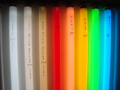
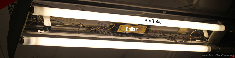
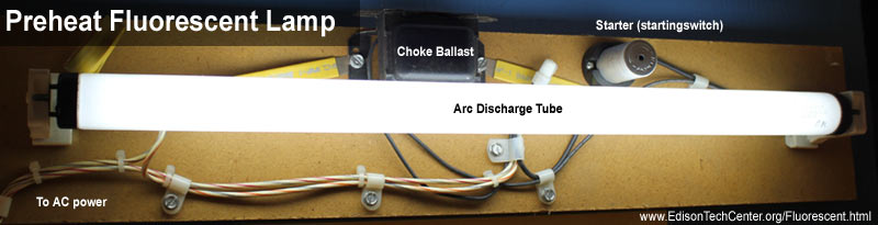
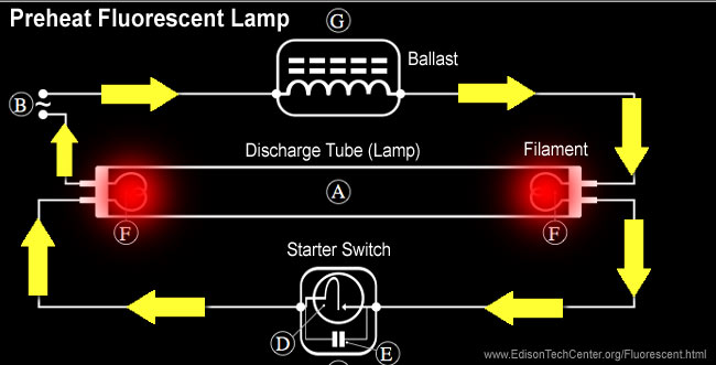

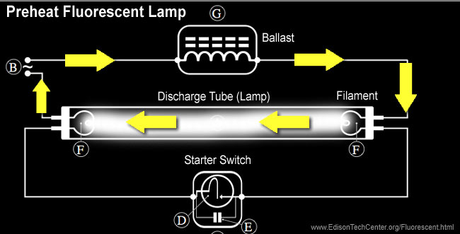
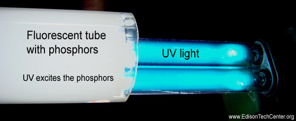

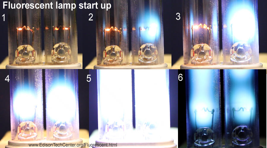
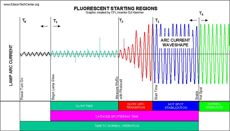
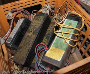
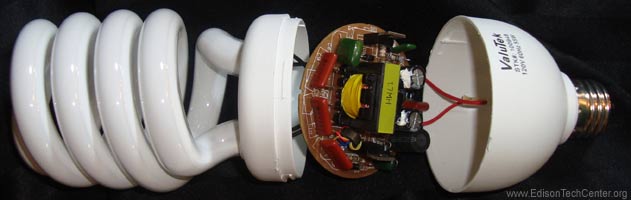
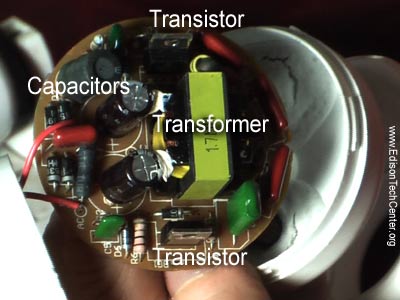
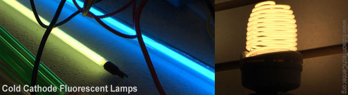
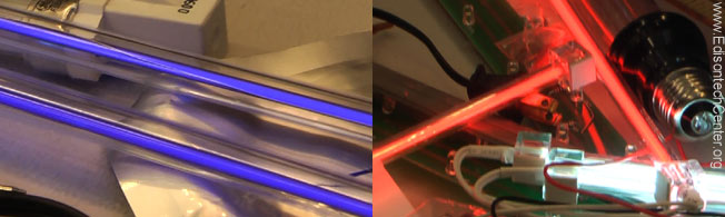
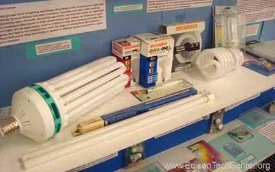
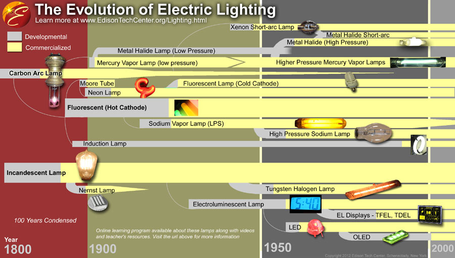


.jpg)


_with_complete_passivation.png)


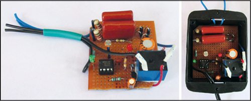
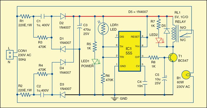
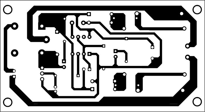
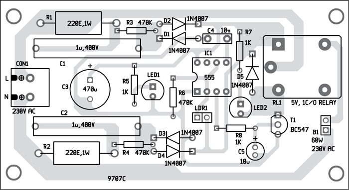


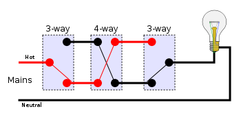
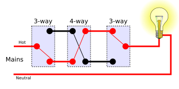
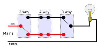


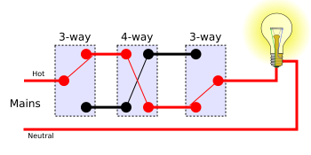


Your blog is very nice and we hope you are providing more information in future time
BalasHapushttps://indusdesignworks.com/structural-engineering.php
Hire structural engineer online