electronic wave guide If do Then If pointers and microwaves on modern electronics Return as like as Strategy and Tactic AMNIMARJESLOW GOVERNMENT 91220017 XI XA PIN PING HUNG CHOP 02096010014 LJBUSAF WAVEGUIDE FOR THEN TRANSMISSION ELECTRONIC GO THEN STRATEGY AND TACTIC OF GLOBAL WARFARE SITUATION CONDITION UNTIL VISION TO MISSION 2020
Waveguides
A waveguide is a special form of transmission line consisting of a hollow, metal tube. The tube wall provides distributed inductance, while the empty space between the tube walls provide distributed capacitance: Figure below
Wave guides conduct microwave energy at lower loss than coaxial cables.
Waveguides are practical only for signals of extremely high frequency, where the wavelength approaches the cross-sectional dimensions of the waveguide. Below such frequencies, waveguides are useless as electrical transmission lines.
When functioning as transmission lines, though, waveguides are considerably simpler than two-conductor cables—especially coaxial cables—in their manufacture and maintenance. With only a single conductor (the waveguide’s “shell”), there are no concerns with proper conductor-to-conductor spacing, or of the consistency of the dielectric material, since the only dielectric in a waveguide is air. Moisture is not as severe a problem in waveguides as it is within coaxial cables, either, and so waveguides are often spared the necessity of gas “filling.”
Waveguides may be thought of as conduits for electromagnetic energy, the waveguide itself acting as nothing more than a “director” of the energy rather than as a signal conductor in the normal sense of the word. In a sense, all transmission lines function as conduits of electromagnetic energy when transporting pulses or high-frequency waves, directing the waves as the banks of a river direct a tidal wave. However, because waveguides are single-conductor elements, the propagation of electrical energy down a waveguide is of a very different nature than the propagation of electrical energy down a two-conductor transmission line.
All electromagnetic waves consist of electric and magnetic fields propagating in the same direction of travel, but perpendicular to each other. Along the length of a normal transmission line, both electric and magnetic fields are perpendicular (transverse) to the direction of wave travel. This is known as the principal mode, or TEM (Transverse Electric and Magnetic) mode. This mode of wave propagation can exist only where there are two conductors, and it is the dominant mode of wave propagation where the cross-sectional dimensions of the transmission line are small compared to the wavelength of the signal. (Figure below)
Twin lead transmission line propagation: TEM mode.
At microwave signal frequencies (between 100 MHz and 300 GHz), two-conductor transmission lines of any substantial length operating in standard TEM mode become impractical. Lines small enough in cross-sectional dimension to maintain TEM mode signal propagation for microwave signals tend to have low voltage ratings, and suffer from large, parasitic power losses due to conductor “skin” and dielectric effects. Fortunately, though, at these short wavelengths there exist other modes of propagation that are not as “lossy,” if a conductive tube is used rather than two parallel conductors. It is at these high frequencies that waveguides become practical.
When an electromagnetic wave propagates down a hollow tube, only one of the fields—either electric or magnetic—will actually be transverse to the wave’s direction of travel. The other field will “loop” longitudinally to the direction of travel, but still be perpendicular to the other field. Whichever field remains transverse to the direction of travel determines whether the wave propagates in TE mode (Transverse Electric) or TM (Transverse Magnetic) mode. (Figure below)
Waveguide (TE) transverse electric and (TM) transverse magnetic modes.
Many variations of each mode exist for a given waveguide, and a full discussion of this is subject well beyond the scope of this book.
Signals are typically introduced to and extracted from waveguides by means of small antenna-like coupling devices inserted into the waveguide. Sometimes these coupling elements take the form of a dipole, which is nothing more than two open-ended stub wires of appropriate length. Other times, the coupler is a single stub (a half-dipole, similar in principle to a “whip” antenna, 1/4λ in physical length), or a short loop of wire terminated on the inside surface of the waveguide: (Figure below)
Stub and loop coupling to waveguide.
In some cases, such as a class of vacuum tube devices called inductive output tubes (the so-called klystron tube falls into this category), a “cavity” formed of conductive material may intercept electromagnetic energy from a modulated beam of electrons, having no contact with the beam itself: (Figure below below)
Klystron inductive output tube.
Just as transmission lines are able to function as resonant elements in a circuit, especially when terminated by a short-circuit or an open-circuit, a dead-ended waveguide may also resonate at particular frequencies. When used as such, the device is called a cavity resonator. Inductive output tubes use toroid-shaped cavity resonators to maximize the power transfer efficiency between the electron beam and the output cable.
A cavity’s resonant frequency may be altered by changing its physical dimensions. To this end, cavities with movable plates, screws, and other mechanical elements for tuning are manufactured to provide coarse resonant frequency adjustment.
If a resonant cavity is made open on one end, it functions as a unidirectional antenna. The following photograph shows a home-made waveguide formed from a tin can, used as an antenna for a 2.4 GHz signal in an “802.11b” computer communication network. The coupling element is a quarter-wave stub: nothing more than a piece of solid copper wire about 1-1/4 inches in length extending from the center of a coaxial cable connector penetrating the side of the can: (Figure below)
Can-tenna illustrates stub coupling to waveguide.
A few more tin-can antennae may be seen in the background, one of them a “Pringles” potato chip can. Although this can is of cardboard (paper) construction, its metallic inner lining provides the necessary conductivity to function as a waveguide. Some of the cans in the background still have their plastic lids in place. The plastic, being nonconductive, does not interfere with the RF signal, but functions as a physical barrier to prevent rain, snow, dust, and other physical contaminants from entering the waveguide. “Real” waveguide antennae use similar barriers to physically enclose the tube, yet allow electromagnetic energy to pass unimpeded.
REVIEW:
Waveguides are metal tubes functioning as “conduits” for carrying electromagnetic waves. They are practical only for signals of extremely high frequency, where the signal wavelength approaches the cross-sectional dimensions of the waveguide.
Wave propagation through a waveguide may be classified into two broad categories: TE (Transverse Electric), or TM (Transverse Magnetic), depending on which field (electric or magnetic) is perpendicular (transverse) to the direction of wave travel. Wave travel along a standard, two-conductor transmission line is of the TEM (Transverse Electric and Magnetic) mode, where both fields are oriented perpendicular to the direction of travel. TEM mode is only possible with two conductors and cannot exist in a waveguide.
A dead-ended waveguide serving as a resonant element in a microwave circuit is called a cavity resonator.
A cavity resonator with an open end functions as a unidirectional antenna, sending or receiving RF energy to/from the direction of the open end.
Impedance Transformation
Standing waves at the resonant frequency points of an open- or short-circuited transmission line produce unusual effects. When the signal frequency is such that exactly 1/2 wave or some multiple thereof matches the line’s length, the source “sees” the load impedance as it is. The following pair of illustrations shows an open-circuited line operating at 1/2 (Figure below)
and 1 wavelength (Figure below) frequencies: Source sees open, same as end of half wavelength line. Source sees open, same as end of full wavelength (2x half wavelength line).
In either case, the line has voltage antinodes at both ends, and current nodes at both ends. That is to say, there is maximum voltage and minimum current at either end of the line, which corresponds to the condition of an open circuit. The fact that this condition exists at both ends of the line tells us that the line faithfully reproduces its terminating impedance at the source end, so that the source “sees” an open circuit where it connects to the transmission line, just as if it were directly open-circuited.
The same is true if the transmission line is terminated by a short: at signal frequencies corresponding to 1/2 wavelength (Figure below) or some multiple (Figure below) thereof, the source “sees” a short circuit, with minimum voltage and maximum current present at the connection points between source and transmission line: Source sees short, same as end of half wave length line. Source sees short, same as end of full wavelength line (2x half wavelength).
However, if the signal frequency is such that the line resonates at 1/4 wavelength or some multiple thereof, the source will “see” the exact opposite of the termination impedance. That is, if the line is open-circuited, the source will “see” a short-circuit at the point where it connects to the line; and if the line is short-circuited, the source will “see” an open circuit: (Figure below) Line open-circuited; source “sees” a short circuit: at quarter wavelength line (Figure below), at three-quarter wavelength line (Figure below) Source sees short, reflected from open at end of quarter wavelength line. Source sees short, reflected from open at end of three-quarter wavelength line. Line short-circuited; source “sees” an open circuit: at quarter wavelength line (Figure below), at three-quarter wavelength line (Figure below) Source sees open, reflected from short at end of quarter wavelength line. Source sees open, reflected from short at end of three-quarter wavelength line.
At these frequencies, the transmission line is actually functioning as an impedance transformer, transforming an infinite impedance into zero impedance, or vice versa. Of course, this only occurs at resonant points resulting in a standing wave of 1/4 cycle (the line’s fundamental, resonant frequency) or some odd multiple (3/4, 5/4, 7/4, 9/4 . . .), but if the signal frequency is known and unchanging, this phenomenon may be used to match otherwise unmatched impedances to each other.
Take for instance the example circuit from the last section where a 75 Ω source connects to a 75 Ω transmission line, terminating in a 100 Ω load impedance. From the numerical figures obtained via SPICE, let’s determine what impedance the source “sees” at its end of the transmission line at the line’s resonant frequencies: quarter wavelength (Figure below), halfwave length (Figure below), three-quarter wavelength (Figure below) full wavelength (Figure below) Source sees 56.25 Ω reflected from 100 Ω load at end of quarter wavelength line. Source sees 100 Ω reflected from 100 Ω load at end of half wavelength line. Source sees 56.25 Ω reflected from 100 Ω load at end of three-quarter wavelength line (same as quarter wavelength).
Source sees 100 Ω reflected from 100 Ω load at end of full-wavelength line (same as half-wavelength).
A simple equation relates line impedance (Z0), load impedance (Zload), and input impedance (Zinput) for an unmatched transmission line operating at an odd harmonic of its fundamental frequency:
One practical application of this principle would be to match a 300 Ω load to a 75 Ω signal source at a frequency of 50 MHz. All we need to do is calculate the proper transmission line impedance (Z0), and length so that exactly 1/4 of a wave will “stand” on the line at a frequency of 50 MHz.
First, calculating the line impedance: taking the 75 Ω we desire the source to “see” at the source-end of the transmission line, and multiplying by the 300 Ω load resistance, we obtain a figure of 22,500. Taking the square root of 22,500 yields 150 Ω for a characteristic line impedance.
Now, to calculate the necessary line length: assuming that our cable has a velocity factor of 0.85, and using a speed-of-light figure of 186,000 miles per second, the velocity of propagation will be 158,100 miles per second. Taking this velocity and dividing by the signal frequency gives us a wavelength of 0.003162 miles, or 16.695 feet. Since we only need one-quarter of this length for the cable to support a quarter-wave, the requisite cable length is 4.1738 feet.
Here is a schematic diagram for the circuit, showing node numbers for the SPICE analysis we’re about to run: (Figure below) Quarter wave section of 150 Ω transmission line matches 75 Ω source to 300 Ω load.
We can specify the cable length in SPICE in terms of time delay from beginning to end. Since the frequency is 50 MHz, the signal period will be the reciprocal of that, or 20 nano-seconds (20 ns). One-quarter of that time (5 ns) will be the time delay of a transmission line one-quarter wavelength long:
Transmission line
v1 1 0 ac 1 sin
rsource 1 2 75
t1 2 0 3 0 z0=150 td=5n
rload 3 0 300
.ac lin 1 50meg 50meg
.print ac v(1,2) v(1) v(2) v(3)
.end
At a frequency of 50 MHz, our 1-volt signal source drops half of its voltage across the series 75 Ω impedance (v(1,2)) and the other half of its voltage across the input terminals of the transmission line (v(2)). This means the source “thinks” it is powering a 75 Ω load. The actual load impedance, however, receives a full 1 volt, as indicated by the 1.000 figure at v(3). With 0.5 volt dropped across 75 Ω, the source is dissipating 3.333 mW of power: the same as dissipated by 1 volt across the 300 Ω load, indicating a perfect match of impedance, according to the Maximum Power Transfer Theorem. The 1/4-wavelength, 150 Ω, transmission line segment has successfully matched the 300 Ω load to the 75 Ω source.
Bear in mind, of course, that this only works for 50 MHz and its odd-numbered harmonics. For any other signal frequency to receive the same benefit of matched impedances, the 150 Ω line would have to lengthened or shortened accordingly so that it was exactly 1/4 wavelength long.
Strangely enough, the exact same line can also match a 75 Ω load to a 300 Ω source, demonstrating how this phenomenon of impedance transformation is fundamentally different in principle from that of a conventional, two-winding transformer:
Transmission line
v1 1 0 ac 1 sin
rsource 1 2 300
t1 2 0 3 0 z0=150 td=5n
rload 3 0 75
.ac lin 1 50meg 50meg
.print ac v(1,2) v(1) v(2) v(3)
.end
Here, we see the 1-volt source voltage equally split between the 300 Ω source impedance (v(1,2)) and the line’s input (v(2)), indicating that the load “appears” as a 300 Ω impedance from the source’s perspective where it connects to the transmission line. This 0.5 volt drop across the source’s 300 Ω internal impedance yields a power figure of 833.33 µW, the same as the 0.25 volts across the 75 Ω load, as indicated by voltage figure v(3). Once again, the impedance values of source and load have been matched by the transmission line segment.
This technique of impedance matching is often used to match the differing impedance values of transmission line and antenna in radio transmitter systems, because the transmitter’s frequency is generally well-known and unchanging. The use of an impedance “transformer” 1/4 wavelength in length provides impedance matching using the shortest conductor length possible. (Figure below) Quarter wave 150 Ω transmission line section matches 75 Ω line to 300 Ω antenna.
REVIEW:
A transmission line with standing waves may be used to match different impedance values if operated at the correct frequency(ies).
When operated at a frequency corresponding to a standing wave of 1/4-wavelength along the transmission line, the line’s characteristic impedance necessary for impedance transformation must be equal to the square root of the product of the source’s impedance and the load’s impedance.
Standing Waves and Resonance
Whenever there is a mismatch of impedance between transmission line and load, reflections will occur. If the incident signal is a continuous AC waveform, these reflections will mix with more of the oncoming incident waveform to produce stationary waveforms called standing waves.
The following illustration shows how a triangle-shaped incident waveform turns into a mirror-image reflection upon reaching the line’s unterminated end. The transmission line in this illustrative sequence is shown as a single, thick line rather than a pair of wires, for simplicity’s sake. The incident wave is shown traveling from left to right, while the reflected wave travels from right to left: (Figure below)
Incident wave reflects off end of unterminated transmission line.
If we add the two waveforms together, we find that a third, stationary waveform is created along the line’s length: (Figure below)
The sum of the incident and reflected waves is a stationary wave.
This third, “standing” wave, in fact, represents the only voltage along the line, being the representative sum of incident and reflected voltage waves. It oscillates in instantaneous magnitude, but does not propagate down the cable’s length like the incident or reflected waveforms causing it. Note the dots along the line length marking the “zero” points of the standing wave (where the incident and reflected waves cancel each other), and how those points never change position: (Figure below)
The standing wave does not propgate along the transmission line.
Standing waves are quite abundant in the physical world. Consider a string or rope, shaken at one end, and tied down at the other (only one half-cycle of hand motion shown, moving downward): (Figure below)
Standing waves on a rope.
Both the nodes (points of little or no vibration) and the antinodes (points of maximum vibration) remain fixed along the length of the string or rope. The effect is most pronounced when the free end is shaken at just the right frequency. Plucked strings exhibit the same “standing wave” behavior, with “nodes” of maximum and minimum vibration along their length. The major difference between a plucked string and a shaken string is that the plucked string supplies its own “correct” frequency of vibration to maximize the standing-wave effect: (Figure below)
Standing waves on a plucked string.
Wind blowing across an open-ended tube also produces standing waves; this time, the waves are vibrations of air molecules (sound) within the tube rather than vibrations of a solid object. Whether the standing wave terminates in a node (minimum amplitude) or an antinode (maximum amplitude) depends on whether the other end of the tube is open or closed: (Figure below)
Standing sound waves in open ended tubes.
A closed tube end must be a wave node, while an open tube end must be an antinode. By analogy, the anchored end of a vibrating string must be a node, while the free end (if there is any) must be an antinode.
Note how there is more than one wavelength suitable for producing standing waves of vibrating air within a tube that precisely match the tube’s end points. This is true for all standing-wave systems: standing waves will resonate with the system for any frequency (wavelength) correlating to the node/antinode points of the system. Another way of saying this is that there are multiple resonant frequencies for any system supporting standing waves.
All higher frequencies are integer-multiples of the lowest (fundamental) frequency for the system. The sequential progression of harmonics from one resonant frequency to the next defines the overtone frequencies for the system: (Figure below)
Harmonics (overtones) in open ended pipes
The actual frequencies (measured in Hertz) for any of these harmonics or overtones depends on the physical length of the tube and the waves’ propagation velocity, which is the speed of sound in air.
Because transmission lines support standing waves, and force these waves to possess nodes and antinodes according to the type of termination impedance at the load end, they also exhibit resonance at frequencies determined by physical length and propagation velocity. Transmission line resonance, though, is a bit more complex than resonance of strings or of air in tubes, because we must consider both voltage waves and current waves.
This complexity is made easier to understand by way of computer simulation. To begin, let’s examine a perfectly matched source, transmission line, and load. All components have an impedance of 75 Ω: (Figure below)
Perfectly matched transmission line.
Using SPICE to simulate the circuit, we’ll specify the transmission line (t1) with a 75 Ω characteristic impedance (z0=75) and a propagation delay of 1 microsecond (td=1u). This is a convenient method for expressing the physical length of a transmission line: the amount of time it takes a wave to propagate down its entire length. If this were a real 75 Ω cable—perhaps a type “RG-59B/U” coaxial cable, the type commonly used for cable television distribution—with a velocity factor of 0.66, it would be about 648 feet long. Since 1 µs is the period of a 1 MHz signal, I’ll choose to sweep the frequency of the AC source from (nearly) zero to that figure, to see how the system reacts when exposed to signals ranging from DC to 1 wavelength.
Here is the SPICE netlist for the circuit shown above:
Transmission line
v1 1 0 ac 1 sin
rsource 1 2 75
t1 2 0 3 0 z0=75 td=1u
rload 3 0 75
.ac lin 101 1m 1meg
* Using ‘‘Nutmeg’’ program to plot analysis
.end
Running this simulation and plotting the source impedance drop (as an indication of current), the source voltage, the line’s source-end voltage, and the load voltage, we see that the source voltage—shown as vm(1) (voltage magnitude between node 1 and the implied ground point of node 0) on the graphic plot—registers a steady 1 volt, while every other voltage registers a steady 0.5 volts: (Figure below)
No resonances on a matched transmission line.
In a system where all impedances are perfectly matched, there can be no standing waves, and therefore no resonant “peaks” or “valleys” in the Bode plot.
Now, let’s change the load impedance to 999 MΩ, to simulate an open-ended transmission line. (Figure below) We should definitely see some reflections on the line now as the frequency is swept from 1 mHz to 1 MHz: (Figure below)
Open ended transmission line.
Transmission line
v1 1 0 ac 1 sin
rsource 1 2 75
t1 2 0 3 0 z0=75 td=1u
rload 3 0 999meg
.ac lin 101 1m 1meg
* Using ‘‘Nutmeg’’ program to plot analysis
.end
Resonances on open transmission line.
Here, both the supply voltage vm(1) and the line’s load-end voltage vm(3) remain steady at 1 volt. The other voltages dip and peak at different frequencies along the sweep range of 1 mHz to 1 MHz. There are five points of interest along the horizontal axis of the analysis: 0 Hz, 250 kHz, 500 kHz, 750 kHz, and 1 MHz. We will investigate each one with regard to voltage and current at different points of the circuit.
At 0 Hz (actually 1 mHz), the signal is practically DC, and the circuit behaves much as it would given a 1-volt DC battery source. There is no circuit current, as indicated by zero voltage drop across the source impedance (Zsource: vm(1,2)), and full source voltage present at the source-end of the transmission line (voltage measured between node 2 and node 0: vm(2)). (Figure below)
At f=0: input: V=1, I=0; end: V=1, I=0.
At 250 kHz, we see zero voltage and maximum current at the source-end of the transmission line, yet still full voltage at the load-end: (Figure below)
At f=250 KHz: input: V=0, I=13.33 mA; end: V=1 I=0.
You might be wondering, how can this be? How can we get full source voltage at the line’s open end while there is zero voltage at its entrance? The answer is found in the paradox of the standing wave. With a source frequency of 250 kHz, the line’s length is precisely right for 1/4 wavelength to fit from end to end. With the line’s load end open-circuited, there can be no current, but there will be voltage. Therefore, the load-end of an open-circuited transmission line is a current node (zero point) and a voltage antinode (maximum amplitude): (Figure below)
Open end of transmission line shows current node, voltage antinode at open end.
At 500 kHz, exactly one-half of a standing wave rests on the transmission line, and here we see another point in the analysis where the source current drops off to nothing and the source-end voltage of the transmission line rises again to full voltage: (Figure below)
Full standing wave on half wave open transmission line.
At 750 kHz, the plot looks a lot like it was at 250 kHz: zero source-end voltage (vm(2)) and maximum current (vm(1,2)). This is due to 3/4 of a wave poised along the transmission line, resulting in the source “seeing” a short-circuit where it connects to the transmission line, even though the other end of the line is open-circuited: (Figure below)
1 1/2 standing waves on 3/4 wave open transmission line.
When the supply frequency sweeps up to 1 MHz, a full standing wave exists on the transmission line. At this point, the source-end of the line experiences the same voltage and current amplitudes as the load-end: full voltage and zero current. In essence, the source “sees” an open circuit at the point where it connects to the transmission line. (Figure below)
Double standing waves on full wave open transmission line.
In a similar fashion, a short-circuited transmission line generates standing waves, although the node and antinode assignments for voltage and current are reversed: at the shorted end of the line, there will be zero voltage (node) and maximum current (antinode). What follows is the SPICE simulation (circuit Figure below and illustrations of what happens (Figure 2nd-below at resonances) at all the interesting frequencies: 0 Hz (Figure below) , 250 kHz (Figure below), 500 kHz (Figure below), 750 kHz (Figure below), and 1 MHz (Figure below). The short-circuit jumper is simulated by a 1 µΩ load impedance: (Figure below)
Shorted transmission line.
Transmission line
v1 1 0 ac 1 sin
rsource 1 2 75
t1 2 0 3 0 z0=75 td=1u
rload 3 0 1u
.ac lin 101 1m 1meg
* Using ‘‘Nutmeg’’ program to plot analysis
.end
Full wave standing wave pattern on half wave shorted transmission line.
1 1/2 standing wavepattern on 3/4 wave shorted transmission line.
Double standing waves on full wave shorted transmission line.
In both these circuit examples, an open-circuited line and a short-circuited line, the energy reflection is total: 100% of the incident wave reaching the line’s end gets reflected back toward the source. If, however, the transmission line is terminated in some impedance other than an open or a short, the reflections will be less intense, as will be the difference between minimum and maximum values of voltage and current along the line.
Suppose we were to terminate our example line with a 100 Ω resistor instead of a 75 Ω resistor. (Figure below) Examine the results of the corresponding SPICE analysis to see the effects of impedance mismatch at different source frequencies: (Figure below)
Transmission line terminated in a mismatch
Transmission line
v1 1 0 ac 1 sin
rsource 1 2 75
t1 2 0 3 0 z0=75 td=1u
rload 3 0 100
.ac lin 101 1m 1meg
* Using ‘‘Nutmeg’’ program to plot analysis
.end
Weak resonances on a mismatched transmission line
If we run another SPICE analysis, this time printing numerical results rather than plotting them, we can discover exactly what is happening at all the interesting frequencies: (DC, Figure below; 250 kHz, Figure below; 500 kHz, Figure below; 750 kHz, Figure below; and 1 MHz, Figure below).
Transmission line
v1 1 0 ac 1 sin
rsource 1 2 75
t1 2 0 3 0 z0=75 td=1u
rload 3 0 100
.ac lin 5 1m 1meg
.print ac v(1,2) v(1) v(2) v(3)
.end
At all frequencies, the source voltage, v(1), remains steady at 1 volt, as it should. The load voltage, v(3), also remains steady, but at a lesser voltage: 0.5714 volts. However, both the line input voltage (v(2)) and the voltage dropped across the source’s 75 Ω impedance (v(1,2), indicating current drawn from the source) vary with frequency.
At odd harmonics of the fundamental frequency (250 kHz, Figure 3rd-above and 750 kHz, Figure above) we see differing levels of voltage at each end of the transmission line, because at those frequencies the standing waves terminate at one end in a node and at the other end in an antinode. Unlike the open-circuited and short-circuited transmission line examples, the maximum and minimum voltage levels along this transmission line do not reach the same extreme values of 0% and 100% source voltage, but we still have points of “minimum” and “maximum” voltage. (Figure 6th-above) The same holds true for current: if the line’s terminating impedance is mismatched to the line’s characteristic impedance, we will have points of minimum and maximum current at certain fixed locations on the line, corresponding to the standing current wave’s nodes and antinodes, respectively.
One way of expressing the severity of standing waves is as a ratio of maximum amplitude (antinode) to minimum amplitude (node), for voltage or for current. When a line is terminated by an open or a short, this standing wave ratio, or SWR is valued at infinity, since the minimum amplitude will be zero, and any finite value divided by zero results in an infinite (actually, “undefined”) quotient. In this example, with a 75 Ω line terminated by a 100 Ω impedance, the SWR will be finite: 1.333, calculated by taking the maximum line voltage at either 250 kHz or 750 kHz (0.5714 volts) and dividing by the minimum line voltage (0.4286 volts).
Standing wave ratio may also be calculated by taking the line’s terminating impedance and the line’s characteristic impedance, and dividing the larger of the two values by the smaller. In this example, the terminating impedance of 100 Ω divided by the characteristic impedance of 75 Ω yields a quotient of exactly 1.333, matching the previous calculation very closely.
A perfectly terminated transmission line will have an SWR of 1, since voltage at any location along the line’s length will be the same, and likewise for current. Again, this is usually considered ideal, not only because reflected waves constitute energy not delivered to the load, but because the high values of voltage and current created by the antinodes of standing waves may over-stress the transmission line’s insulation (high voltage) and conductors (high current), respectively.
Also, a transmission line with a high SWR tends to act as an antenna, radiating electromagnetic energy away from the line, rather than channeling all of it to the load. This is usually undesirable, as the radiated energy may “couple” with nearby conductors, producing signal interference. An interesting footnote to this point is that antenna structures—which typically resemble open- or short-circuited transmission lines—are often designed to operate at high standing wave ratios, for the very reason of maximizing signal radiation and reception.
The following photograph (Figure below) shows a set of transmission lines at a junction point in a radio transmitter system. The large, copper tubes with ceramic insulator caps at the ends are rigid coaxial transmission lines of 50 Ω characteristic impedance. These lines carry RF power from the radio transmitter circuit to a small, wooden shelter at the base of an antenna structure, and from that shelter on to other shelters with other antenna structures:
Flexible coaxial cables connected to rigid lines.
Flexible coaxial cable connected to the rigid lines (also of 50 Ω characteristic impedance) conduct the RF power to capacitive and inductive “phasing” networks inside the shelter. The white, plastic tube joining two of the rigid lines together carries “filling” gas from one sealed line to the other. The lines are gas-filled to avoid collecting moisture inside them, which would be a definite problem for a coaxial line. Note the flat, copper “straps” used as jumper wires to connect the conductors of the flexible coaxial cables to the conductors of the rigid lines. Why flat straps of copper and not round wires? Because of the skin effect, which renders most of the cross-sectional area of a round conductor useless at radio frequencies.
Like many transmission lines, these are operated at low SWR conditions. As we will see in the next section, though, the phenomenon of standing waves in transmission lines is not always undesirable, as it may be exploited to perform a useful function: impedance transformation.
REVIEW:
Standing waves are waves of voltage and current which do not propagate (i.e. they are stationary), but are the result of interference between incident and reflected waves along a transmission line.
A node is a point on a standing wave of minimum amplitude.
An antinode is a point on a standing wave of maximum amplitude.
Standing waves can only exist in a transmission line when the terminating impedance does not match the line’s characteristic impedance. In a perfectly terminated line, there are no reflected waves, and therefore no standing waves at all.
At certain frequencies, the nodes and antinodes of standing waves will correlate with the ends of a transmission line, resulting in resonance.
The lowest-frequency resonant point on a transmission line is where the line is one quarter-wavelength long. Resonant points exist at every harmonic (integer-multiple) frequency of the fundamental (quarter-wavelength).
Standing wave ratio, or SWR, is the ratio of maximum standing wave amplitude to minimum standing wave amplitude. It may also be calculated by dividing termination impedance by characteristic impedance, or vice versa, which ever yields the greatest quotient. A line with no standing waves (perfectly matched: Zload to Z0) has an SWR equal to 1.
Transmission lines may be damaged by the high maximum amplitudes of standing waves. Voltage antinodes may break down insulation between conductors, and current antinodes may overheat conductors.
“Long’’ and “Short’’ Transmission Lines
In DC and low-frequency AC circuits, the characteristic impedance of parallel wires is usually ignored. This includes the use of coaxial cables in instrument circuits, often employed to protect weak voltage signals from being corrupted by induced “noise” caused by stray electric and magnetic fields. This is due to the relatively short timespans in which reflections take place in the line, as compared to the period of the waveforms or pulses of the significant signals in the circuit. As we saw in the last section, if a transmission line is connected to a DC voltage source, it will behave as a resistor equal in value to the line’s characteristic impedance only for as long as it takes the incident pulse to reach the end of the line and return as a reflected pulse, back to the source. After that time (a brief 16.292 µs for the mile-long coaxial cable of the last example), the source “sees” only the terminating impedance, whatever that may be.
If the circuit in question handles low-frequency AC power, such short time delays introduced by a transmission line between when the AC source outputs a voltage peak and when the source “sees” that peak loaded by the terminating impedance (round-trip time for the incident wave to reach the line’s end and reflect back to the source) are of little consequence. Even though we know that signal magnitudes along the line’s length are not equal at any given time due to signal propagation at (nearly) the speed of light, the actual phase difference between start-of-line and end-of-line signals is negligible, because line-length propagations occur within a very small fraction of the AC waveform’s period. For all practical purposes, we can say that voltage along all respective points on a low-frequency, two-conductor line are equal and in-phase with each other at any given point in time.
In these cases, we can say that the transmission lines in question are electrically short, because their propagation effects are much quicker than the periods of the conducted signals. By contrast, an electrically long line is one where the propagation time is a large fraction or even a multiple of the signal period. A “long” line is generally considered to be one where the source’s signal waveform completes at least a quarter-cycle (90o of “rotation”) before the incident signal reaches line’s end. Up until this chapter in the Lessons In Electric Circuits book series, all connecting lines were assumed to be electrically short.
To put this into perspective, we need to express the distance traveled by a voltage or current signal along a transmission line in relation to its source frequency. An AC waveform with a frequency of 60 Hz completes one cycle in 16.66 ms. At light speed (186,000 mile/s), this equates to a distance of 3100 miles that a voltage or current signal will propagate in that time. If the velocity factor of the transmission line is less than 1, the propagation velocity will be less than 186,000 miles per second, and the distance less by the same factor. But even if we used the coaxial cable’s velocity factor from the last example (0.66), the distance is still a very long 2046 miles! Whatever distance we calculate for a given frequency is called the wavelength of the signal.
A simple formula for calculating wavelength is as follows:
The lower-case Greek letter “lambda” (λ) represents wavelength, in whatever unit of length used in the velocity figure (if miles per second, then wavelength in miles; if meters per second, then wavelength in meters). Velocity of propagation is usually the speed of light when calculating signal wavelength in open air or in a vacuum, but will be less if the transmission line has a velocity factor less than 1.
If a “long” line is considered to be one at least 1/4 wavelength in length, you can see why all connecting lines in the circuits discussed thusfar have been assumed “short.” For a 60 Hz AC power system, power lines would have to exceed 775 miles in length before the effects of propagation time became significant. Cables connecting an audio amplifier to speakers would have to be over 4.65 miles in length before line reflections would significantly impact a 10 kHz audio signal!
When dealing with radio-frequency systems, though, transmission line length is far from trivial. Consider a 100 MHz radio signal: its wavelength is a mere 9.8202 feet, even at the full propagation velocity of light (186,000 mile/s). A transmission line carrying this signal would not have to be more than about 2-1/2 feet in length to be considered “long!” With a cable velocity factor of 0.66, this critical length shrinks to 1.62 feet.
When an electrical source is connected to a load via a “short” transmission line, the load’s impedance dominates the circuit. This is to say, when the line is short, its own characteristic impedance is of little consequence to the circuit’s behavior. We see this when testing a coaxial cable with an ohmmeter: the cable reads “open” from center conductor to outer conductor if the cable end is left unterminated. Though the line acts as a resistor for a very brief period of time after the meter is connected (about 50 Ω for an RG-58/U cable), it immediately thereafter behaves as a simple “open circuit:” the impedance of the line’s open end. Since the combined response time of an ohmmeter and the human being using it greatly exceeds the round-trip propagation time up and down the cable, it is “electrically short” for this application, and we only register the terminating (load) impedance. It is the extreme speed of the propagated signal that makes us unable to detect the cable’s 50 Ω transient impedance with an ohmmeter.
If we use a coaxial cable to conduct a DC voltage or current to a load, and no component in the circuit is capable of measuring or responding quickly enough to “notice” a reflected wave, the cable is considered “electrically short” and its impedance is irrelevant to circuit function. Note how the electrical “shortness” of a cable is relative to the application: in a DC circuit where voltage and current values change slowly, nearly any physical length of cable would be considered “short” from the standpoint of characteristic impedance and reflected waves. Taking the same length of cable, though, and using it to conduct a high-frequency AC signal could result in a vastly different assessment of that cable’s “shortness!”
When a source is connected to a load via a “long” transmission line, the line’s own characteristic impedance dominates over load impedance in determining circuit behavior. In other words, an electrically “long” line acts as the principal component in the circuit, its own characteristics overshadowing the load’s. With a source connected to one end of the cable and a load to the other, current drawn from the source is a function primarily of the line and not the load. This is increasingly true the longer the transmission line is. Consider our hypothetical 50 Ω cable of infinite length, surely the ultimate example of a “long” transmission line: no matter what kind of load we connect to one end of this line, the source (connected to the other end) will only see 50 Ω of impedance, because the line’s infinite length prevents the signal from ever reaching the end where the load is connected. In this scenario, line impedance exclusively defines circuit behavior, rendering the load completely irrelevant.
The most effective way to minimize the impact of transmission line length on circuit behavior is to match the line’s characteristic impedance to the load impedance. If the load impedance is equal to the line impedance, then any signal source connected to the other end of the line will “see” the exact same impedance, and will have the exact same amount of current drawn from it, regardless of line length. In this condition of perfect impedance matching, line length only affects the amount of time delay from signal departure at the source to signal arrival at the load. However, perfect matching of line and load impedances is not always practical or possible.
The next section discusses the effects of “long” transmission lines, especially when line length happens to match specific fractions or multiples of signal wavelength.
REVIEW:
Coaxial cabling is sometimes used in DC and low-frequency AC circuits as well as in high-frequency circuits, for the excellent immunity to induced “noise” that it provides for signals.
When the period of a transmitted voltage or current signal greatly exceeds the propagation time for a transmission line, the line is considered electrically short. Conversely, when the propagation time is a large fraction or multiple of the signal’s period, the line is considered electrically long.
A signal’s wavelength is the physical distance it will propagate in the timespan of one period. Wavelength is calculated by the formula λ=v/f, where “λ” is the wavelength, “v” is the propagation velocity, and “f” is the signal frequency.
A rule-of-thumb for transmission line “shortness” is that the line must be at least 1/4 wavelength before it is considered “long.”
In a circuit with a “short” line, the terminating (load) impedance dominates circuit behavior. The source effectively sees nothing but the load’s impedance, barring any resistive losses in the transmission line.
In a circuit with a “long” line, the line’s own characteristic impedance dominates circuit behavior. The ultimate example of this is a transmission line of infinite length: since the signal will never reach the load impedance, the source only “sees” the cable’s characteristic impedance.
When a transmission line is terminated by a load precisely matching its impedance, there are no reflected waves and thus no problems with line length.
A transmission line of infinite length is an interesting abstraction, but physically impossible. All transmission lines have some finite length, and as such do not behave precisely the same as an infinite line. If that piece of 50 Ω “RG-58/U” cable I measured with an ohmmeter years ago had been infinitely long, I actually would have been able to measure 50 Ω worth of resistance between the inner and outer conductors. But it was not infinite in length, and so it measured as “open” (infinite resistance).
Nonetheless, the characteristic impedance rating of a transmission line is important even when dealing with limited lengths. An older term for characteristic impedance, which I like for its descriptive value, is surge impedance. If a transient voltage (a “surge”) is applied to the end of a transmission line, the line will draw a current proportional to the surge voltage magnitude divided by the line’s surge impedance (I=E/Z). This simple, Ohm’s Law relationship between current and voltage will hold true for a limited period of time, but not indefinitely.
If the end of a transmission line is open-circuited—that is, left unconnected—the current “wave” propagating down the line’s length will have to stop at the end, since electrons cannot flow where there is no continuing path. This abrupt cessation of current at the line’s end causes a “pile-up” to occur along the length of the transmission line, as the electrons successively find no place to go. Imagine a train traveling down the track with slack between the rail car couplings: if the lead car suddenly crashes into an immovable barricade, it will come to a stop, causing the one behind it to come to a stop as soon as the first coupling slack is taken up, which causes the next rail car to stop as soon as the next coupling’s slack is taken up, and so on until the last rail car stops. The train does not come to a halt together, but rather in sequence from first car to last: (Figure below)
Reflected wave.
A signal propagating from the source-end of a transmission line to the load-end is called an incident wave. The propagation of a signal from load-end to source-end (such as what happened in this example with current encountering the end of an open-circuited transmission line) is called a reflected wave.
When this electron “pile-up” propagates back to the battery, current at the battery ceases, and the line acts as a simple open circuit. All this happens very quickly for transmission lines of reasonable length, and so an ohmmeter measurement of the line never reveals the brief time period where the line actually behaves as a resistor. For a mile-long cable with a velocity factor of 0.66 (signal propagation velocity is 66% of light speed, or 122,760 miles per second), it takes only 1/122,760 of a second (8.146 microseconds) for a signal to travel from one end to the other. For the current signal to reach the line’s end and “reflect” back to the source, the round-trip time is twice this figure, or 16.292 µs.
High-speed measurement instruments are able to detect this transit time from source to line-end and back to source again, and may be used for the purpose of determining a cable’s length. This technique may also be used for determining the presence and location of a break in one or both of the cable’s conductors, since a current will “reflect” off the wire break just as it will off the end of an open-circuited cable. Instruments designed for such purposes are called time-domain reflectometers (TDRs). The basic principle is identical to that of sonar range-finding: generating a sound pulse and measuring the time it takes for the echo to return.
A similar phenomenon takes place if the end of a transmission line is short-circuited: when the voltage wave-front reaches the end of the line, it is reflected back to the source, because voltage cannot exist between two electrically common points. When this reflected wave reaches the source, the source sees the entire transmission line as a short-circuit. Again, this happens as quickly as the signal can propagate round-trip down and up the transmission line at whatever velocity allowed by the dielectric material between the line’s conductors.
A simple experiment illustrates the phenomenon of wave reflection in transmission lines. Take a length of rope by one end and “whip” it with a rapid up-and-down motion of the wrist. A wave may be seen traveling down the rope’s length until it dissipates entirely due to friction: (Figure below)
Lossy transmission line.
This is analogous to a long transmission line with internal loss: the signal steadily grows weaker as it propagates down the line’s length, never reflecting back to the source. However, if the far end of the rope is secured to a solid object at a point prior to the incident wave’s total dissipation, a second wave will be reflected back to your hand: (Figure below)
Reflected wave.
Usually, the purpose of a transmission line is to convey electrical energy from one point to another. Even if the signals are intended for information only, and not to power some significant load device, the ideal situation would be for all of the original signal energy to travel from the source to the load, and then be completely absorbed or dissipated by the load for maximum signal-to-noise ratio. Thus, “loss” along the length of a transmission line is undesirable, as are reflected waves, since reflected energy is energy not delivered to the end device.
Reflections may be eliminated from the transmission line if the load’s impedance exactly equals the characteristic (“surge”) impedance of the line. For example, a 50 Ω coaxial cable that is either open-circuited or short-circuited will reflect all of the incident energy back to the source. However, if a 50 Ω resistor is connected at the end of the cable, there will be no reflected energy, all signal energy being dissipated by the resistor.
This makes perfect sense if we return to our hypothetical, infinite-length transmission line example. A transmission line of 50 Ω characteristic impedance and infinite length behaves exactly like a 50 Ω resistance as measured from one end. (Figure below)
If we cut this line to some finite length, it will behave as a 50 Ω resistor to a constant source of DC voltage for a brief time, but then behave like an open- or a short-circuit, depending on what condition we leave the cut end of the line: open (Figure below)
or shorted. (Figure below)
However, if we terminate the line with a 50 Ω resistor, the line will once again behave as a 50 Ω resistor, indefinitely: the same as if it were of infinite length again: (Figure below)
Infinite transmission line looks like resistor.
One mile transmission.
Shorted transmission line.
Line terminated in characteristic impedance.
In essence, a terminating resistor matching the natural impedance of the transmission line makes the line “appear” infinitely long from the perspective of the source, because a resistor has the ability to eternally dissipate energy in the same way a transmission line of infinite length is able to eternally absorb energy.
Reflected waves will also manifest if the terminating resistance isn’t precisely equal to the characteristic impedance of the transmission line, not just if the line is left unconnected (open) or jumpered (shorted). Though the energy reflection will not be total with a terminating impedance of slight mismatch, it will be partial. This happens whether or not the terminating resistance is greater or less than the line’s characteristic impedance.
Re-reflections of a reflected wave may also occur at the source end of a transmission line, if the source’s internal impedance (Thevenin equivalent impedance) is not exactly equal to the line’s characteristic impedance. A reflected wave returning back to the source will be dissipated entirely if the source impedance matches the line’s, but will be reflected back toward the line end like another incident wave, at least partially, if the source impedance does not match the line. This type of reflection may be particularly troublesome, as it makes it appear that the source has transmitted another pulse.
REVIEW:
Characteristic impedance is also known as surge impedance, due to the temporarily resistive behavior of any length transmission line.
A finite-length transmission line will appear to a DC voltage source as a constant resistance for some short time, then as whatever impedance the line is terminated with. Therefore, an open-ended cable simply reads “open” when measured with an ohmmeter, and “shorted” when its end is short-circuited.
A transient (“surge”) signal applied to one end of an open-ended or short-circuited transmission line will “reflect” off the far end of the line as a secondary wave. A signal traveling on a transmission line from source to load is called an incident wave; a signal “bounced” off the end of a transmission line, traveling from load to source, is called a reflected wave.
Reflected waves will also appear in transmission lines terminated by resistors not precisely matching the characteristic impedance.
A finite-length transmission line may be made to appear infinite in length if terminated by a resistor of equal value to the line’s characteristic impedance. This eliminates all signal reflections.
A reflected wave may become re-reflected off the source-end of a transmission line if the source’s internal impedance does not match the line’s characteristic impedance. This re-reflected wave will appear, of course, like another pulse signal transmitted from the source.
Suppose, though, that we had a set of parallel wires of infinite length, with no lamp at the end. What would happen when we close the switch? Being that there is no longer a load at the end of the wires, this circuit is open. Would there be no current at all? (Figure below)
Driving an infinite transmission line.
Despite being able to avoid wire resistance through the use of superconductors in this “thought experiment,” we cannot eliminate capacitance along the wires’ lengths. Any pair of conductors separated by an insulating medium creates capacitance between those conductors: (Figure below)
Equivalent circuit showing stray capacitance between conductors.
Voltage applied between two conductors creates an electric field between those conductors. Energy is stored in this electric field, and this storage of energy results in an opposition to change in voltage. The reaction of a capacitance against changes in voltage is described by the equation i = C(de/dt), which tells us that current will be drawn proportional to the voltage’s rate of change over time. Thus, when the switch is closed, the capacitance between conductors will react against the sudden voltage increase by charging up and drawing current from the source. According to the equation, an instant rise in applied voltage (as produced by perfect switch closure) gives rise to an infinite charging current.
However, the current drawn by a pair of parallel wires will not be infinite, because there exists series impedance along the wires due to inductance. (Figure below) Remember that current through any conductor develops a magnetic field of proportional magnitude. Energy is stored in this magnetic field, (Figure below) and this storage of energy results in an opposition to change in current. Each wire develops a magnetic field as it carries charging current for the capacitance between the wires, and in so doing drops voltage according to the inductance equation e = L(di/dt). This voltage drop limits the voltage rate-of-change across the distributed capacitance, preventing the current from ever reaching an infinite magnitude:
Equivalent circuit showing stray capacitance and inductance.
Voltage charges capacitance, current charges inductance.
Because the electrons in the two wires transfer motion to and from each other at nearly the speed of light, the “wave front” of voltage and current change will propagate down the length of the wires at that same velocity, resulting in the distributed capacitance and inductance progressively charging to full voltage and current, respectively, like this: (Figures below, below, below, below)
Uncharged transmission line.
Begin wave propagation.
Continue wave propagation.
Propagate at speed of light.
The end result of these interactions is a constant current of limited magnitude through the battery source. Since the wires are infinitely long, their distributed capacitance will never fully charge to the source voltage, and their distributed inductance will never allow unlimited charging current. In other words, this pair of wires will draw current from the source so long as the switch is closed, behaving as a constant load. No longer are the wires merely conductors of electrical current and carriers of voltage, but now constitute a circuit component in themselves, with unique characteristics. No longer are the two wires merely a pair of conductors, but rather a transmission line.
As a constant load, the transmission line’s response to applied voltage is resistive rather than reactive, despite being comprised purely of inductance and capacitance (assuming superconducting wires with zero resistance). We can say this because there is no difference from the battery’s perspective between a resistor eternally dissipating energy and an infinite transmission line eternally absorbing energy. The impedance (resistance) of this line in ohms is called the characteristic impedance, and it is fixed by the geometry of the two conductors. For a parallel-wire line with air insulation, the characteristic impedance may be calculated as such:
If the transmission line is coaxial in construction, the characteristic impedance follows a different equation:
In both equations, identical units of measurement must be used in both terms of the fraction. If the insulating material is other than air (or a vacuum), both the characteristic impedance and the propagation velocity will be affected. The ratio of a transmission line’s true propagation velocity and the speed of light in a vacuum is called the velocity factor of that line.
Velocity factor is purely a factor of the insulating material’s relative permittivity (otherwise known as its dielectric constant), defined as the ratio of a material’s electric field permittivity to that of a pure vacuum. The velocity factor of any cable type—coaxial or otherwise—may be calculated quite simply by the following formula:
Characteristic impedance is also known as natural impedance, and it refers to the equivalent resistance of a transmission line if it were infinitely long, owing to distributed capacitance and inductance as the voltage and current “waves” propagate along its length at a propagation velocity equal to some large fraction of light speed.
It can be seen in either of the first two equations that a transmission line’s characteristic impedance (Z0) increases as the conductor spacing increases. If the conductors are moved away from each other, the distributed capacitance will decrease (greater spacing between capacitor “plates”), and the distributed inductance will increase (less cancellation of the two opposing magnetic fields). Less parallel capacitance and more series inductance results in a smaller current drawn by the line for any given amount of applied voltage, which by definition is a greater impedance. Conversely, bringing the two conductors closer together increases the parallel capacitance and decreases the series inductance. Both changes result in a larger current drawn for a given applied voltage, equating to a lesser impedance.
Barring any dissipative effects such as dielectric “leakage” and conductor resistance, the characteristic impedance of a transmission line is equal to the square root of the ratio of the line’s inductance per unit length divided by the line’s capacitance per unit length:
REVIEW:
A transmission line is a pair of parallel conductors exhibiting certain characteristics due to distributed capacitance and inductance along its length.
When a voltage is suddenly applied to one end of a transmission line, both a voltage “wave” and a current “wave” propagate along the line at nearly light speed.
If a DC voltage is applied to one end of an infinitely long transmission line, the line will draw current from the DC source as though it were a constant resistance.
The characteristic impedance (Z0) of a transmission line is the resistance it would exhibit if it were infinite in length. This is entirely different from leakage resistance of the dielectric separating the two conductors, and the metallic resistance of the wires themselves. Characteristic impedance is purely a function of the capacitance and inductance distributed along the line’s length, and would exist even if the dielectric were perfect (infinite parallel resistance) and the wires superconducting (zero series resistance).
Velocity factor is a fractional value relating a transmission line’s propagation speed to the speed of light in a vacuum. Values range between 0.66 and 0.80 for typical two-wire lines and coaxial cables. For any cable type, it is equal to the reciprocal (1/x) of the square root of the relative permittivity of the cable’s insulation.
Suppose we had a simple one-battery, one-lamp circuit controlled by a switch. When the switch is closed, the lamp immediately lights. When the switch is opened, the lamp immediately darkens: (Figure below)
Lamp appears to immediately respond to switch.
Actually, an incandescent lamp takes a short time for its filament to warm up and emit light after receiving an electric current of sufficient magnitude to power it, so the effect is not instant. However, what I’d like to focus on is the immediacy of the electric current itself, not the response time of the lamp filament. For all practical purposes, the effect of switch action is instant at the lamp’s location. Although electrons move through wires very slowly, the overall effect of electrons pushing against each other happens at the speed of light (approximately 186,000 miles per second!).
What would happen, though, if the wires carrying power to the lamp were 186,000 miles long? Since we know the effects of electricity do have a finite speed (albeit very fast), a set of very long wires should introduce a time delay into the circuit, delaying the switch’s action on the lamp: (Figure below)
At the speed of light, lamp responds after 1 second.
Assuming no warm-up time for the lamp filament, and no resistance along the 372,000 mile length of both wires, the lamp would light up approximately one second after the switch closure. Although the construction and operation of superconducting wires 372,000 miles in length would pose enormous practical problems, it is theoretically possible, and so this “thought experiment” is valid. When the switch is opened again, the lamp will continue to receive power for one second of time after the switch opens, then it will de-energize.
One way of envisioning this is to imagine the electrons within a conductor as rail cars in a train: linked together with a small amount of “slack” or “play” in the couplings. When one rail car (electron) begins to move, it pushes on the one ahead of it and pulls on the one behind it, but not before the slack is relieved from the couplings. Thus, motion is transferred from car to car (from electron to electron) at a maximum velocity limited by the coupling slack, resulting in a much faster transfer of motion from the left end of the train (circuit) to the right end than the actual speed of the cars (electrons): (Figure below)
Motion is transmitted sucessively from one car to next.
Another analogy, perhaps more fitting for the subject of transmission lines, is that of waves in water. Suppose a flat, wall-shaped object is suddenly moved horizontally along the surface of water, so as to produce a wave ahead of it. The wave will travel as water molecules bump into each other, transferring wave motion along the water’s surface far faster than the water molecules themselves are actually traveling: (Figure below)
Wave motion in water.
Likewise, electron motion “coupling” travels approximately at the speed of light, although the electrons themselves don’t move that quickly. In a very long circuit, this “coupling” speed would become noticeable to a human observer in the form of a short time delay between switch action and lamp action.
REVIEW:
In an electric circuit, the effects of electron motion travel approximately at the speed of light, although electrons within the conductors do not travel anywhere near that velocity.
Early in my explorations of electricity, I came across a length of coaxial cable with the label “50 ohms” printed along its outer sheath. (Figure below) Now, coaxial cable is a two-conductor cable made of a single conductor surrounded by a braided wire jacket, with a plastic insulating material separating the two. As such, the outer (braided) conductor completely surrounds the inner (single wire) conductor, the two conductors insulated from each other for the entire length of the cable. This type of cabling is often used to conduct weak (low-amplitude) voltage signals, due to its excellent ability to shield such signals from external interference.
Coaxial cable contruction.
I was mystified by the “50 ohms” label on this coaxial cable. How could two conductors, insulated from each other by a relatively thick layer of plastic, have 50 ohms of resistance between them? Measuring resistance between the outer and inner conductors with my ohmmeter, I found it to be infinite (open-circuit), just as I would have expected from two insulated conductors. Measuring each of the two conductors’ resistances from one end of the cable to the other indicated nearly zero ohms of resistance: again, exactly what I would have expected from continuous, unbroken lengths of wire. Nowhere was I able to measure 50 Ω of resistance on this cable, regardless of which points I connected my ohmmeter between.
What I didn’t understand at the time was the cable’s response to short-duration voltage “pulses” and high-frequency AC signals. Continuous direct current (DC)—such as that used by my ohmmeter to check the cable’s resistance—shows the two conductors to be completely insulated from each other, with nearly infinite resistance between the two. However, due to the effects of capacitance and inductance distributed along the length of the cable, the cable’s response to rapidly-changing voltages is such that it acts as a finite impedance, drawing current proportional to an applied voltage. What we would normally dismiss as being just a pair of wires becomes an important circuit element in the presence of transient and high-frequency AC signals, with characteristic properties all its own. When expressing such properties, we refer to the wire pair as a transmission line.
This chapter explores transmission line behavior. Many transmission line effects do not appear in significant measure in AC circuits of powerline frequency (50 or 60 Hz), or in continuous DC circuits, and so we haven’t had to concern ourselves with them in our study of electric circuits thus far. However, in circuits involving high frequencies and/or extremely long cable lengths, the effects are very significant. Practical applications of transmission line effects abound in radio-frequency (“RF”) communication circuitry, including computer networks, and in low-frequency circuits subject to voltage transients (“surges”) such as lightning strikes on power lines.
XXX . XXX WAVE GUIDE
A waveguide is a structure that guides waves, such as electromagnetic waves or sound, with minimal loss of energy by restricting expansion to one dimension or two. There is a similar effect in water waves constrained within a canal, or guns that have barrels which restrict hot gas expansion to maximize energy transfer to their bullets. Without the physical constraint of a waveguide, wave amplitudes decrease according to the inverse square law as they expand into three dimensional space.
There are different types of waveguides for each type of wave. The original and most common[1] meaning is a hollow conductive metal pipe used to carry high frequency radio waves, particularly microwaves.
The geometry of a waveguide reflects its function. Slab waveguides confine energy in one dimension, fiber or channel waveguides in two dimensions. The frequency of the transmitted wave also dictates the shape of a waveguide: an optical fiber guiding high-frequencylight will not guide microwaves of a much lower frequency. As a rule of thumb, the width of a waveguide needs to be of the same order of magnitude as the wavelength of the guided wave.
Some naturally occurring structures can also act as waveguides. The SOFAR channel layer in the ocean can guide the sound of whale song across enormous distances .
Example of waveguides and a diplexer in an air traffic control radar
Waves propagate in all directions in open space as spherical waves. The power of the wave falls with the distance R from the source as the square of the distance (inverse square law). A waveguide confines the wave to propagate in one dimension, so that, under ideal conditions, the wave loses no power while propagating. Due to total reflection at the walls, waves are confined to the interior of a waveguide.
Flash Back
The first structure for guiding waves was proposed by J. J. Thomson in 1893, and was first experimentally tested by Oliver Lodge in 1894. The first mathematical analysis of electromagnetic waves in a metal cylinder was performed by Lord Rayleigh in 1897. For sound waves, Lord Rayleigh published a full mathematical analysis of propagation modes in his seminal work, “The Theory of Sound”. Jagadish Chandra Bose researched millimetre wavelengths using waveguides, and in 1897 described to the Royal Institution in London his research carried out in Kolkata.
The study of dielectric waveguides (such as optical fibers, see below) began as early as the 1920s, by several people, most famous of which are Rayleigh, Sommerfeld and Debye. Optical fiber began to receive special attention in the 1960s due to its importance to the communications industry.
The development of radio communication initially occurred at the lower frequencies because these could be more easily propagated over large distances. The long wavelengths made these frequencies unsuitable for use in hollow metal waveguides because of the impractically large diameter tubes required. Consequently, research into hollow metal waveguides stalled and the work of Lord Rayleigh was forgotten for a time and had to be rediscovered by others. Practical investigations resumed in the 1930s by George C. Southworth at Bell Labs and Wilmer L. Barrow at MIT. Southworth at first took the theory from papers on waves in dielectric rods because the work of Lord Rayleigh was unknown to him. This misled him somewhat; some of his experiments failed because he was not aware of the phenomenon of waveguide cutoff frequency already found in Lord Rayleigh's work. Serious theoretical work was taken up by John R. Carson and Sallie P. Mead. This work led to the discovery that for the TE01 mode in circular waveguide losses go down with frequency and at one time this was a serious contender for the format for long distance telecommunications.
The importance of radar in World War II gave a great impetus to waveguide research, at least on the Allied side. The magnetron developed in 1940 by John Randall and Harry Boot at the University of Birmingham in the United Kingdom provided a good power source and made microwave radars feasible. The most important centre of research was at the Radiation Laboratory (Rad Lab) at MIT but many others took part in the US, and in the UK such as the Telecommunications Research Establishment. The head of the Fundamental Development Group at Rad Lab was Edward Mills Purcell. His researchers included Julian Schwinger, Nathan Marcuvitz, Carol Gray Montgomery, and Robert H. Dicke. Much of the Rad Lab work concentrated on finding lumped element models of waveguide structures so that components in waveguide could be analysed with standard circuit theory. Hans Bethe was also briefly at Rad Lab, but while there he produced his small aperture theory which proved important for waveguide cavity filters, first developed at Rad Lab. The German side, on the other hand, largely ignored the potential of waveguides in radar until very late in the war. So much so that when radar parts from a downed British plane were sent to Siemens & Halske for analysis, even though they were recognised as microwave components, their purpose could not be identified.
At that time, microwave techniques were badly neglected in Germany. It was generally believed that it was of no use for electronic warfare, and those who wanted to do research work in this field were not allowed to do so.
— H. Mayer, wartime vice-president of Siemens & Halske
German academics were even allowed to continue publicly publishing their research in this field because it was not felt to be important.
Immediately after World War II waveguide was the technology of choice in the microwave field. However, it has some problems; it is bulky, expensive to produce, and the cutoff frequency effect makes it difficult to produce wideband devices. Ridged waveguide can increase bandwidth beyond an octave, but a better solution is to use a technology working in TEM mode (that is, non-waveguide) such as coaxial conductors since TEM does not have a cutoff frequency. A shielded rectangular conductor can also be used and this has certain manufacturing advantages over coax and can be seen as the forerunner of the planar technologies (stripline and microstrip). However, planar technologies really started to take off when printed circuits were introduced. These methods are significantly cheaper than waveguide and have largely taken its place in most bands. However, waveguide is still favoured in the higher microwave bands from around Ku band upwards.
The uses of waveguides for transmitting signals were known even before the term was coined. The phenomenon of sound waves guided through a taut wire have been known for a long time, as well as sound through a hollow pipe such as a cave or medical stethoscope. Other uses of waveguides are in transmitting power between the components of a system such as radio, radar or optical devices. Waveguides are the fundamental principle of guided wave testing (GWT), one of the many methods of non-destructive evaluation.
Specific examples:
Optical fibers transmit light and signals for long distances with low attenuation and a wide usable range of wavelengths.
In a microwave oven a waveguide transfers power from the magnetron, where waves are formed, to the cooking chamber.
In a radar, a waveguide transfers radio frequency energy to and from the antenna, where the impedance needs to be matched for efficient power transmission (see below).
Rectangular and Circular waveguides are commonly used to connect feeds of parabolic dishes to their electronics, either low-noise receivers or power amplifier/transmitters.
Waveguides are used in scientific instruments to measure optical, acoustic and elastic properties of materials and objects. The waveguide can be put in contact with the specimen (as in a medical ultrasonography), in which case the waveguide ensures that the power of the testing wave is conserved, or the specimen may be put inside the waveguide (as in a dielectric constant measurement), so that smaller objects can be tested and the accuracy is better.
Transmission lines are a specific type of waveguide, very commonly used.
Propagation modes and cutoff frequencies
A propagation mode in a waveguide is one solution of the wave equations, or, in other words, the form of the wave.[6] Due to the constraints of the boundary conditions, there are only limited frequencies and forms for the wave function which can propagate in the waveguide. The lowest frequency in which a certain mode can propagate is the cutoff frequency of that mode. The mode with the lowest cutoff frequency is the fundamental mode of the waveguide, and its cutoff frequency is the waveguide cutoff frequency.
Propagation modes are computed by solving the Helmholtz equation alongside a set of boundary conditions depending on the geometrical shape and materials bounding the region. The usual assumption for infinitely long uniform waveguides allows to assume a propagating form for the wave, i.e. stating that every field component has a known dependency on the propagation direction (i.e. ). More specifically, the common approach is to first replace all unknown time-varying unknown fields (assuming for simplicity to describe the fields in cartesian components) with their complex phasors representation , sufficient to fully describe any infinitely long single-tone signal at frequency , (angular frequency ), and rewrite the Helmholtz equation and boundary conditions accordingly. Then, every unknown field is forced to have a form like , where the term represents the propagation constant (still unknown) along the direction along which the waveguide extends to infinity. The Helmholtz equation can be rewritten to accommodate such form and the resulting equality needs to be solved for and , yielding in the end an eigenvalue equation for and a corresponding eigenfunction for each solution of the former.[11]
The propagation constant of the guided wave is complex, in general. For a lossless case, the propagation constant might be found to take on either real or imaginary values, depending on the chosen solution of the eigenvalue equation and on the angular frequency . When is purely real, the mode is said to be "below cutoff", since the amplitude of the field phasors tends to exponentially decrease with propagation; an imaginary , instead, represents modes said to be "in propagation" or "above cutoff", as the complex amplitude of the phasors does not change with .[12]
Impedance matching
In circuit theory, the impedance is a generalization of electrical resistivity in the case of alternating current, and is measured in ohms ().A waveguide in circuit theory is described by a transmission line having a length and characteristic impedance. In other words, the impedance indicates the ratio of voltage to current of the circuit component (in this case a waveguide) during propagation of the wave. This description of the waveguide was originally intended for alternating current, but is also suitable for electromagnetic and sound waves, once the wave and material properties (such as pressure, density, dielectric constant) are properly converted into electrical terms (current and impedance for example).
Impedance matching is important when components of an electric circuit are connected (waveguide to antenna for example): The impedance ratio determines how much of the wave is transmitted forward and how much is reflected. In connecting a waveguide to an antenna a complete transmission is usually required, so an effort is made to match their impedances.
The reflection coefficient can be calculated using: , where is the reflection coefficient (0 denotes full transmission, 1 full reflection, and 0.5 is a reflection of half the incoming voltage), and are the impedance of the first component (from which the wave enters) and the second component, respectively.
An impedance mismatch creates a reflected wave, which added to the incoming waves creates a standing wave. An impedance mismatch can be also quantified with the standing wave ratio (SWR or VSWR for voltage), which is connected to the impedance ratio and reflection coefficient by: , where are the minimum and maximum values of the voltage absolute value, and the VSWR is the voltage standing wave ratio, which value of 1 denotes full transmission, without reflection and thus no standing wave, while very large values mean high reflection and standing wave pattern.
Electromagnetic waveguides
Waveguides can be constructed to carry waves over a wide portion of the electromagnetic spectrum, but are especially useful in the microwave and optical frequency ranges. Depending on the frequency, they can be constructed from either conductive or dielectric materials. Waveguides are used for transferring both power and communication signals.
In this military radar, microwave radiation is transmitted between the source and the reflector by a waveguide. The figure suggests that microwaves leave the box in a circularly symmetric mode (allowing the antenna to rotate), then they are converted to a linear mode, and pass through a flexible stage. Their polarisation is then rotated in a twisted stage and finally they irradiate the parabolic antenna.
Optical waveguides
Waveguides used at optical frequencies are typically dielectric waveguides, structures in which a dielectric material with high permittivity, and thus high index of refraction, is surrounded by a material with lower permittivity. The structure guides optical waves by total internal reflection. An example of an optical waveguide is optical fiber.
Other types of optical waveguide are also used, including photonic-crystal fiber, which guides waves by any of several distinct mechanisms. Guides in the form of a hollow tube with a highly reflective inner surface have also been used as light pipes for illumination applications. The inner surfaces may be polished metal, or may be covered with a multilayer film that guides light by Bragg reflection (this is a special case of a photonic-crystal fiber). One can also use small prisms around the pipe which reflect light via total internal reflection —such confinement is necessarily imperfect, however, since total internal reflection can never truly guide light within a lower-index core (in the prism case, some light leaks out at the prism corners).
Acoustic waveguides
An acoustic waveguide is a physical structure for guiding sound waves. A duct for sound propagation also behaves like a transmission line. The duct contains some medium, such as air, that supports sound propagation.
Mathematical waveguides
Waveguides are interesting objects of study from a strictly mathematical perspective. A waveguide (or tube) is defined as type of boundary condition on the wave equation such that the wave function must be equal to zero on the boundary and that the allowed region is finite in all dimensions but one (an infinitely long cylinder is an example.) A large number of interesting results can be proven from these general conditions. It turns out that any tube with a bulge (where the width of the tube increases) admits at least one bound state. This can be shown using the variational principles. An interesting result by Jeffrey Goldstone and Robert Jaffe[13] is that any tube of constant width with a twist, admits a bound state.
An orthomode transducer (OMT) is a waveguide component. It is commonly referred to as a polarisation duplexer. Orthomode transducers serve either to combine or to separate two orthogonallypolarized microwave signal paths.[1] One of the paths forms the uplink, which is transmitted over the same waveguide as the received signal path, or downlink path. Such a device may be part of a VSATantenna feed or a terrestrial microwave radio feed; for example, OMTs are often used with a feed horn to isolate orthogonal polarizations of a signal and to transfer transmit and receive signals to different ports .
For VSAT modems the transmission and reception paths are at 90° to each other, or in other words, the signals are orthogonally polarized with respect to each other. This orthogonal shift between the two signal paths provides approximately an isolation of 40 dB in the Ku band and Ka band radio frequency bands. Hence this device serves in an essential role as the junction element of the outdoor unit (ODU) of a VSAT modem. It protects the receiver front-end element (the low-noise block converter, LNB) from burn-out by the power of the output signal generated by the block up converter (BUC). The BUC is also connected to the feed horn through a wave guide port of the OMT junction device. Orthomode transducers are used in dual-polarized Very small aperture terminals (VSATs), in sparsely populated areas, radar antennas, radiometers, and communications links. They are usually connected to the antenna's down converter or LNB and to the High Power Amplifier (HPA) attached to a transmitting antenna. Wherever there are two polarizations of radio signals (Horizontal and Vertical), the transmitted and received radio signal to and from the antenna are said to be “orthogonal”. This means that the modulation planes of the two radio signal waves are at 90 degrees angles to each other. The OMT device is used to separate two equal frequency signals, of high and low signal power. Protective separation is essential as the transmitter unit would seriously damage the very sensitive low micro-voltage (µV), front-end receiver amplifier unit at the antenna. The transmission signal of the up-link, of relatively high power (1, 2,or 5 watts for common VSAT equipment) originating from BUC (block up converter), and the very low power received signal power (µV) coming from the antenna (aerial) to the LNB receiver unit, in this case are at an angle of 90° relative to each other, are both coupled together at the feed-horn focal-point of the Parabolic antenna. The device that unites both up-link and down-link paths, which are at 90° to each other, is known as an Orthogonal Mode Transducer OMT. In the VSAT Ku band of operation case, a typical OMT Orthomode Transducer provides a 40 dB isolation between each of the connected radio ports to the feed horn that faces the parabolic dish reflector (40 dB means that only 0.01% of the transmitter's output power is cross-fed into the receiver's wave guide port). The port facing the parabolic reflector of the antenna is a circular polarizing port so that horizontal and vertical polarity coupling of inbound and outbound radio signal is easily achieved. The 40 dB isolation provides essential protection to the very sensitive receiver amplifier against burn out from the relatively high-power signal of the transmitter unit. Further isolation may be obtained by means of selective radio frequency filtering to achieve an isolation of 100 dB (100 dB means that only a 10−10 fraction of the transmitter's output power is cross-fed into the wave guide port of the receiver). The second image demonstrates two types of outdoor units, a 1-watt Hughes unit and a composite configuration of a 2-watt BUC/OMT/LNB Andrew, Swedish Microwave units. The following images show a Portenseigne & Hirschmann Ku band configuration, that highlights the horizontal the vertical, and circular polarized wave-guide ports that join to the Feed-horn, the LNB or BUC elements of an outdoor unit.
Terrestrial Microwave
An ortho-mode transducer is also a component commonly found on high capacity terrestrial microwave radio links. In this arrangement, two parabolic reflector dishes operate in a point to point microwave radio path (4 GHz to 85 GHz) with four radios, two mounted on each end. On each dish a T-shaped ortho-mode transducer is mounted at the rear of the feed, separating the signal from the feed into two separate radios, one operating in the horizontal polarity, and the other in the vertical polarity. This arrangement is used to increase the aggregate data throughput between two dishes on a point to point microwave path, or for fault-tolerance redundancy. Certain types of outdoor microwave radios have integrated orthomode transducers and operate in both polarities from a single radio unit, performing cross-polarization interference cancellation (XPIC) within the radio unit itself.
Orthomode transducer (Portenseigne, France)
Orthomode transducer, vertical and horizontal polarity
Antenna side of OMT
Training
VSAT specific training that demonstrates the use of the Orthomode Transducer (OMT):
Characterization
An ortho-mode transducer can be modelled as a 4-port device, 2 of these (H and V) representing the single-polarization ports and the remaining (h, v) embodied by the degenerate modes in the dual-polarized port.
The scattering parameters can be gathered in a 4×4 scattering matrix , which is symmetrical for a reciprocal OMT (i.e. not including circulators, isolators or active components), thus leaving 10 independent terms for a general lossy device:
Of these:
4 (, , , ) represent the intrinsic reflection terms of the 4 ports, related to the return loss when all the ports are closed onto ideal loads equal to the port characteristic impedance;
2 (, ) are the main direct transmission terms (from each single-polarization port to the corresponding mode on the dual-polarized port);
2 (, ) represent the cross-polarization discrimination (XPD): from each single-polarization port to the supposedly-isolated mode on the dual-polarized port;
2 (, ) model the isolation terms (sometimes referred as inter-port isolation, IPI): between the two single-polarized ports and between the two orthogonal modes at the dual-polarized port.
An ideal OMT exhibits perfect matching (null terms on the diagonal), unitary direct transmission terms and infinite XPD and isolation (null corresponding scattering parameters):
Characterization of a manufactured OMT (considered the device under test, DUT) is usually a delicate matter for both mechanical and theoretical reasons.
Conceptually, if an ideal OMT is available as part of the measurement setup, often named "golden sample", its dual-polarized port can be connected to its counterpart on the DUT, resulting in a 4-port equivalent device with 4 single-polarization ports. The ideal OMT splits the two polarizations at the dual-polarized port into two standard single-polarized ports and such arrangement allows the direct measurement of all the scattering parameters of the DUT (either by using a 4-port vector network analyzer (VNA) or a 2-port one with 2 single-polarized loads used in several combinations).
Such ideal setup is only prone to mechanical uncertainties related to the physical placement and alignment of the dual-polarized ports. A simple misalignment angle introduces an artificial path from each polarization to the opposite proportional to . The phasorial combination of the leakage (or ) due to the XPDs of DUT and this artificial loss is the actual external measured quantity. If, by proper phase recombination, the two contributions tend to cancel each other, the actual measured XPD can increase to infinity (possible only if ), thus resulting in a huge estimation error.
Depending on the expected XPD of the DUT, mechanical countermeasures should be introduced to guarantee that the artificial measurement uncertainty can be neglected.
Any deviation from this ideal setup, however, introduces errors and uncertainties.
If a dual-polarization matched load is available in place of the ideal OMT, this allows 2×2 measurements from the single-polarization ports, yielding only 2 of the reflection terms ( and ) and one IPI (). Other measurements aimed at gaining estimations of the other scattering parameters of the DUT involve the dual-polarized port and require additional components, such as dual-polarized to single-polarized transitions or tapers, which are often not matched on at least one of the two polarizations: this creates undesired reflections which propagate through the OMT and combine at the VNA ports thus preventing direct measurements. These issues add to mechanical factors and enhance uncertainties in the measurement procedure.
Due to the increasing demand for high-capacity data links, the exploitation of dual-polarization has fostered research in design and characterization of OMTs to overcome the practical difficulties. The literature concerning OMT modelling and practical characterization consists of works both by academic organizations such as the National Research Council (Italy), Marche Polytechnic University and European Space Agency and likewise by industrial teams such as CommScope and Siae Micro elettronica with immediate impact on products for modern dual-polarized telecommunication systems, for instance in terrestrial microwavebackhauling.
In electromagnetics and communications engineering, the term waveguide may refer to any linear structure that conveys electromagnetic waves between its endpoints. However, the original and most common meaning is a hollow metal pipe used to carry radio waves. This type of waveguide is used as a transmission line mostly at microwave frequencies, for such purposes as connecting microwave transmitters and receivers to their antennas, in equipment such as microwave ovens, radar sets, satellite communications, and microwave radio links.
A dielectric waveguide employs a solid dielectric rod rather than a hollow pipe. An optical fibre is a dielectric guide designed to work at optical frequencies. Transmission lines such as microstrip, coplanar waveguide, stripline or coaxial cable may also be considered to be waveguides.
The electromagnetic waves in a (metal-pipe) waveguide may be imagined as travelling down the guide in a zig-zag path, being repeatedly reflected between opposite walls of the guide. For the particular case of rectangular waveguide, it is possible to base an exact analysis on this view. Propagation in a dielectric waveguide may be viewed in the same way, with the waves confined to the dielectric by total internal reflection at its surface. Some structures, such as non-radiative dielectric waveguides and the Goubau line, use both metal walls and dielectric surfaces to confine the wave.
Collection of standard waveguide components.
Principle of operation
Example of waveguides and a diplexer in an air traffic control radar
Depending on the frequency, waveguides can be constructed from either conductive or dielectric materials. Generally, the lower the frequency to be passed the larger the waveguide is. For example, the natural waveguide the earth forms given by the dimensions between the conductive ionosphere and the ground as well as the circumference at the median altitude of the Earth is resonant at 7.83 Hz. This is known as Schumann resonance. On the other hand, waveguides used in extremely high frequency (EHF) communications can be less than a millimeter in width.
Analysis
Electromagnetic waveguides are analyzed by solving Maxwell's equations, or their reduced form, the electromagnetic wave equation, with boundary conditions determined by the properties of the materials and their interfaces. These equations have multiple solutions, or modes, which are eigenfunctions of the equation system. Each mode is characterized by a cutoff frequency below which the mode cannot exist in the guide. Waveguide propagation modes depend on the operating wavelength and polarization and the shape and size of the guide. The longitudinal mode of a waveguide is a particular standing wave pattern formed by waves confined in the cavity. The transverse modes are classified into different types:
TE modes (transverse electric) have no electric field in the direction of propagation.
TM modes (transverse magnetic) have no magnetic field in the direction of propagation.
TEM modes (transverse electromagnetic) have no electric nor magnetic field in the direction of propagation.
Hybrid modes have both electric and magnetic field components in the direction of propagation.
In hollow waveguides (single conductor), TEM waves are not possible, since Maxwell's Equations will give that the electric field must then have zero divergence and zero curl and be equal to zero at boundaries, resulting in a zero field (or, equivalently, with boundary conditions guaranteeing only the trivial solution). This contrasts with two-conductor transmission lines used at lower frequencies; coaxial cable, parallel wire line and stripline, in which TEM mode is possible. Additionally, the propagating modes (i.e. TE and TM) inside the waveguide can be mathematically expressed as the superposition of TEM waves.
The mode with the lowest cutoff frequency is termed the dominant mode of the guide. It is common to choose the size of the guide such that only this one mode can exist in the frequency band of operation. In rectangular and circular (hollow pipe) waveguides, the dominant modes are designated the TE1,0 mode and TE1,1 modes respectively.
Rectangular waveguide TE-1,0 mode
B-field, view towards cross-section.
B-field, view from the side.
E-field, view towards cross-section.
Rectangular waveguide TE-0,1 mode
B-field, view towards cross-section.
B-field, view from the side.
E-field, view towards cross-section.
TE1,1 mode of a circular hollow metallic waveguide.
In the microwave region of the electromagnetic spectrum, a waveguide normally consists of a hollow metallic conductor. These waveguides can take the form of single conductors with or without a dielectric coating, e.g. the Goubau line and helical waveguides. Hollow waveguides must be one-half wavelength or more in diameter in order to support one or more transverse wave modes.
Waveguides may be filled with pressurized gas to inhibit arcing and prevent multipaction, allowing higher power transmission. Conversely, waveguides may be required to be evacuated as part of evacuated systems (e.g. electron beam systems).
A slotted waveguide is generally used for radar and other similar applications. The waveguide serves as a feed path, and each slot is a separate radiator, thus forming an antenna. This structure has the capability of generating a radiation pattern to launch an electromagnetic wave in a specific relatively narrow and controllable direction.
A closed waveguide is an electromagnetic waveguide (a) that is tubular, usually with a circular or rectangular cross section, (b) that has electrically conducting walls, (c) that may be hollow or filled with a dielectric material, (d) that can support a large number of discrete propagating modes, though only a few may be practical, (e) in which each discrete mode defines the propagation constant for that mode, (f) in which the field at any point is describable in terms of the supported modes, (g) in which there is no radiation field, and (h) in which discontinuities and bends may cause mode conversion but not radiation.
The dimensions of a hollow metallic waveguide determine which wavelengths it can support, and in which modes. Typically the waveguide is operated so that only a single mode is present. The lowest order mode possible is generally selected. Frequencies below the guide's cutoff frequency will not propagate. It is possible to operate waveguides at higher order modes, or with multiple modes present, but this is usually impractical.
Waveguides are almost exclusively made of metal and mostly rigid structures. There are certain types of "corrugated" waveguides that have the ability to flex and bend but only used where essential since they degrade propagation properties. Due to propagation of energy in mostly air or space within the waveguide, it is one of the lowest loss transmission line types and highly preferred for high frequency applications where most other types of transmission structures introduce large losses. Due to the skin effect at high frequencies, electric current along the walls penetrates typically only a few micrometers into the metal of the inner surface. Since this is where most of the resistive loss occurs, it is important that the conductivity of interior surface be kept as high as possible. For this reason, most waveguide interior surfaces are plated with copper, silver, or gold.
Voltage standing wave ratio (VSWR) measurements may be taken to ensure that a waveguide is contiguous and has no leaks or sharp bends. If such bends or holes in the waveguide surface are present, this may diminish the performance of both transmitter and receiver equipment connected at either end. Poor transmission through the waveguide may also occur as a result of moisture build up which corrodes and degrades conductivity of the inner surfaces, which is crucial for low loss propagation. For this reason, waveguides are nominally fitted with microwave windows at the outer end that will not interfere with propagation but keep the elements out. Moisture can also cause fungus build up or arcing in high power systems such as radio or radar transmitters. Moisture in waveguides can typically be prevented with silica gel, a desiccant, or slight pressurization of the waveguide cavities with dry nitrogen or argon. Desiccant silica gel canisters may be attached with screw-on nibs and higher power systems will have pressurized tanks for maintaining pressure including leakage monitors. Arcing may also occur if there is a hole, tear or bump in the conducting walls, if transmitting at high power (usually 200 watts or more). Waveguide plumbing[14] is crucial for proper waveguide performance. Voltage standing waves occur when impedance mismatches in the waveguide cause energy to reflect back in the opposite direction of propagation. In addition to limiting the effective transfer of energy, these reflections can cause higher voltages in the waveguide and damage equipment.
In practice, waveguides act as the equivalent of cables for super high frequency (SHF) systems. For such applications, it is desired to operate waveguides with only one mode propagating through the waveguide. With rectangular waveguides, it is possible to design the waveguide such that the frequency band over which only one mode propagates is as high as 2:1 (i.e. the ratio of the upper band edge to lower band edge is two). The relation between the waveguide dimensions and the lowest frequency is simple: if is the greater of its two dimensions, then the longest wavelength that will propagate is and the lowest frequency is thus
With circular waveguides, the highest possible bandwidth allowing only a single mode to propagate is only 1.3601:1.
Because rectangular waveguides have a much larger bandwidth over which only a single mode can propagate, standards exist for rectangular waveguides, but not for circular waveguides. In general (but not always), standard waveguides are designed such that
one band starts where another band ends, with another band that overlaps the two bands
the lower edge of the band is approximately 30% higher than the waveguide's cutoff frequency
the upper edge of the band is approximately 5% lower than the cutoff frequency of the next higher order mode
the waveguide height is half the waveguide width
The first condition is to allow for applications near band edges. The second condition limits dispersion, a phenomenon in which the velocity of propagation is a function of frequency. It also limits the loss per unit length. The third condition is to avoid evanescent-wave coupling via higher order modes. The fourth condition is that which allows a 2:1 operation bandwidth. Although it is possible to have a 2:1 operating bandwidth when the height is less than half the width, having the height exactly half the width maximizes the power that can propagate inside the waveguide before dielectric breakdown occurs.
Below is a table of standard waveguides. The waveguide name WR stands for waveguide rectangular, and the number is the inner dimension width of the waveguide in hundredths of an inch (0.01 inch = 0.254 mm) rounded to the nearest hundredth of an inch.
† For historical reasons the outside rather than the inside dimensions of these waveguides are 2:1 (with wall thickness WG6–WG10: 0.08" (2.0 mm), WG11A–WG15: 0.064" (1.6 mm), WG16–WG17: 0.05" (1.3 mm), WG18–WG28: 0.04" (1.0 mm))
For the frequencies in the table above, the main advantage of waveguides over coaxial cables is that waveguides support propagation with lower loss. For lower frequencies, the waveguide dimensions become impractically large, and for higher frequencies the dimensions become impractically small (the manufacturing tolerance becomes a significant portion of the waveguide size).
Dielectric waveguides
Dielectric rod and slab waveguides are used to conduct radio waves, mostly at millimeter wave frequencies and above. These confine the radio waves by total internal reflection from the step in refractive index due to the change in dielectric constant at the material surface.[20] At millimeter wave frequencies and above, metal is not a good conductor, so metal waveguides can have increasing attenuation. At these wavelengths dielectric waveguides can have lower losses than metal waveguides. Optical fiber is a form of dielectric waveguide used at optical wavelengths.
One difference between dielectric and metal waveguides is that at a metal surface the electromagnetic waves are tightly confined; at high frequencies the electric and magnetic fields penetrate a very short distance into the metal. In contrast, the surface of the dielectric waveguide is an interface between two dielectrics, so the fields of the wave penetrate outside the dielectric in the form of an evanescent (non-propagating) wave.
Waveguide rotary joint
A waveguide rotary joint is used in microwave communications to connect two different types of RF waveguides. Because coaxial parts are symmetrical in ø direction, free rotation without performance degradation is accomplished. In the rotating part, electrical continuity is achieved by λ/4-chokes eliminating metal contacts. The Rotary Joints can have both waveguide ports at a right angle to the rotational axis, "U-style", one waveguide port at a right angle and one in line, "L-style" or both waveguide ports in line. "I-style". Waveguide Rotary Joint modules are available for all frequency bands .
Waveguide filter
Figure 1. Waveguide post filter: a band-pass filter consisting of a length of WG15 (a standard waveguide size for X band use) divided into a row of five coupledresonant cavities by fences of three posts each. The ends of the posts can be seen protruding through the wall of the guide.
A waveguide filter is an electronic filter that is constructed with waveguide technology. Waveguides are hollow metal tubes inside which an electromagnetic wave may be transmitted. Filters are devices used to allow signals at some frequencies to pass (the passband), while others are rejected (the stopband). Filters are a basic component of electronic engineering designs and have numerous applications. These include selection of signals and limitation of noise. Waveguide filters are most useful in the microwave band of frequencies, where they are a convenient size and have low loss. Examples of microwave filter use are found in satellite communications, telephone networks, and television broadcasting.
Waveguide filters were developed during World War II to meet the needs of radar and electronic countermeasures, but afterwards soon found civilian applications such as use in microwave links. Much of post-war development was concerned with reducing the bulk and weight of these filters, first by using new analysis techniques that led to elimination of unnecessary components, then by innovations such as dual-mode cavities and novel materials such as ceramic resonators.
A particular feature of waveguide filter design concerns the mode of transmission. Systems based on pairs of conducting wires and similar technologies have only one mode of transmission. In waveguide systems, any number of modes are possible. This can be both a disadvantage, as spurious modes frequently cause problems, and an advantage, as a dual-mode design can be much smaller than the equivalent waveguide single mode design. The chief advantages of waveguide filters over other technologies are their ability to handle high power and their low loss. The chief disadvantages are their bulk and cost when compared with technologies such as microstrip filters.
There is a wide array of different types of waveguide filters. Many of them consist of a chain of coupled resonators of some kind that can be modelled as a ladder network of LC circuits. One of the most common types consists of a number of coupled resonant cavities. Even within this type, there are many subtypes, mostly differentiated by the means of coupling. These coupling types include apertures,[w] irises,[x] and posts. Other waveguide filter types include dielectric resonator filters, insert filters, finline filters, corrugated-waveguide filters, and stub filters. A number of waveguide components have filter theory applied to their design, but their purpose is something other than to filter signals. Such devices include impedance matching components, directional couplers, and diplexers. These devices frequently take on the form of a filter, at least in part.
Scope
The common meaning of waveguide, when the term is used unqualified, is the hollow metal kind, but other waveguide technologies are possible.[1] The scope of this article is limited to the metal-tube type. The post-wall waveguide structure is something of a variant, but is related enough to include in this article—the wave is mostly surrounded by conducting material. It is possible to construct waveguides out of dielectric rods,[2] the most well known example being optical fibres. This subject is outside the scope of the article with the exception that dielectric rod resonators are sometimes used inside hollow metal waveguides. Transmission line[o] technologies such as conducting wires and microstrip can be thought of as waveguides,[3] but are not commonly called such and are also outside the scope of this article.
Waveguides are metal conduits used to confine and direct radio signals. They are usually made of brass, but aluminium and copper are also used.[5] Most commonly they are rectangular, but other cross-sections such as circular or elliptical are possible. A waveguide filter is a filter composed of waveguide components. It has much the same range of applications as other filter technologies in electronics and radio engineering but is very different mechanically and in principle of operation.
The technology used for constructing filters is chosen to a large extent by the frequency of operation that is expected, although there is a large amount of overlap. Low frequency applications such as audio electronics use filters composed of discrete capacitors and inductors. Somewhere in the very high frequency band, designers switch to using components made of pieces of transmission line.These kinds of designs are called distributed element filters. Filters made from discrete components are sometimes called lumped element filters to distinguish them. At still higher frequencies, the microwave bands, the design switches to waveguide filters, or sometimes a combination of waveguides and transmission lines.
Waveguide filters have much more in common with transmission line filters than lumped element filters; they do not contain any discrete capacitors or inductors. However, the waveguide design may frequently be equivalent (or approximately so) to a lumped element design. Indeed, the design of waveguide filters frequently starts from a lumped element design and then converts the elements of that design into waveguide components.
Modes
Figure 2. The field patterns of some common waveguide modes
One of the most important differences in the operation of waveguide filters compared to transmission line designs concerns the mode of transmission of the electromagnetic wave carrying the signal. In a transmission line, the wave is associated with electric currents on a pair of conductors. The conductors constrain the currents to be parallel to the line, and consequently both the magnetic and electric components of the electromagnetic field are perpendicular to the direction of travel of the wave. This transverse mode is designated TEM[l] (transverse electromagnetic). On the other hand, there are infinitely many modes that any completely hollow waveguide can support, but the TEM mode is not one of them. Waveguide modes are designated either TE[m] (transverse electric) or TM(transverse magnetic), followed by a pair of suffixes identifying the precise mode.
This multiplicity of modes can cause problems in waveguide filters when spurious modes are generated. Designs are usually based on a single mode and frequently incorporate features to suppress the unwanted modes. On the other hand, advantage can be had from choosing the right mode for the application, and even sometimes making use of more than one mode at once. Where only a single mode is in use, the waveguide can be modelled like a conducting transmission line and results from transmission line theory can be applied.
Cutoff
Another feature peculiar to waveguide filters is that there is a definite frequency, the cutoff frequency, below which no transmission can take place. This means that in theory low-pass filters cannot be made in waveguides. However, designers frequently take a lumped element low-pass filter design and convert it to a waveguide implementation. The filter is consequently low-pass by design and may be considered a low-pass filter for all practical purposes if the cutoff frequency is below any frequency of interest to the application. The waveguide cutoff frequency is a function of transmission mode, so at a given frequency, the waveguide may be usable in some modes but not others. Likewise, the guide wavelength[h] (λg) and characteristic impedance[b] (Z0) of the guide at a given frequency also depend on mode.
Dominant mode
The mode with the lowest cutoff frequency of all the modes is called the dominant mode. Between cutoff and the next highest mode, this is the only mode it is possible to transmit, which is why it is described as dominant. Any spurious modes generated are rapidly attenuated along the length of the guide and soon disappear. Practical filter designs are frequently made to operate in the dominant mode.
In rectangular waveguide, the TE10[q] mode (shown in figure 2) is the dominant mode. There is a band of frequencies between the dominant mode cutoff and the next highest mode cutoff in which the waveguide can be operated without any possibility of generating spurious modes. The next highest cutoff modes are TE20,[r] at exactly twice the TE10 mode, and TE01[s] which is also twice TE10 if the waveguide used has the commonly used aspect ratio of 2:1. The lowest cutoff TM mode is TM11 (shown in figure 2) which is times the dominant mode in 2:1 waveguide. Thus, there is an octave over which the dominant mode is free of spurious modes, although operating too close to cutoff is usually avoided because of phase distortion.
In circular waveguide, the dominant mode is TE11 and is shown in figure 2. The next highest mode is TM01.[v] The range over which the dominant mode is guaranteed to be spurious-mode free is less than that in rectangular waveguide; the ratio of highest to lowest frequency is approximately 1.3 in circular waveguide, compared to 2.0 in rectangular guide.
Evanescent modes
Evanescent modes are modes below the cutoff frequency. They cannot propagate down the waveguide for any distance, dying away exponentially. However, they are important in the functioning of certain filter components such as irises and posts, described later, because energy is stored in the evanescent wave fields.
Advantages and disadvantages
Like transmission line filters, waveguide filters always have multiple passbands, replicas of the lumped element prototype. In most designs, only the lowest frequency passband is useful (or lowest two in the case of band-stop filters) and the rest are considered unwanted spurious artefacts. This is an intrinsic property of the technology and cannot be designed out, although design can have some control over the frequency position of the spurious bands. Consequently, in any given filter design, there is an upper frequency beyond which the filter will fail to carry out its function. For this reason, true low-pass and high-pass filters cannot exist in waveguide. At some high frequency there will be a spurious passband or stopband interrupting the intended function of the filter. But, similar to the situation with waveguide cutoff frequency, the filter can be designed so that the edge of the first spurious band is well above any frequency of interest.
The range of frequencies over which waveguide filters are useful is largely determined by the waveguide size needed. At lower frequencies the waveguide needs to be impractically large in order to keep the cutoff frequency below the operational frequency. On the other hand, filters whose operating frequencies are so high that the wavelengths are sub-millimetre cannot be manufactured with normal machine shop processes. At frequencies this high, fibre-optic technology starts to become an option.
Waveguides are a low-loss medium. Losses in waveguides mostly come from ohmic dissipation caused by currents induced in the waveguide walls. Rectangular waveguide has lower loss than circular waveguide and is usually the preferred format, but the TE01 circular mode is very low loss and has applications in long distance communications. Losses can be reduced by polishing the internal surfaces of the waveguide walls. In some applications which require rigorous filtering, the walls are plated with a thin layer of gold or silver to improve surface conductivity. An example of such requirements is satellite applications which require low loss, high selectivity, and linear group delay from their filters.
One of the main advantages of waveguide filters over TEM mode technologies is the quality of their resonators. Resonator quality is characterised by a parameter called Q factor, or just Q. The Q of waveguide resonators is in the thousands, orders of magnitude higher than TEM mode resonators. The resistance of conductors, especially in wound inductors, limits the Q of TEM resonators. This improved Q leads to better performing filters in waveguides, with greater stop band rejection. The limitation to Q in waveguides comes mostly from the ohmic losses in the walls described earlier, but silver plating the internal walls can more than double Q.
Waveguides have good power handling capability, which leads to filter applications in radar.Despite the performance advantages of waveguide filters, microstrip is often the preferred technology due to its low cost. This is especially true for consumer items and the lower microwave frequencies. Microstrip circuits can be manufactured by cheap printed circuit technology, and when integrated on the same printed board as other circuit blocks they incur little additional cost
Designs in the 1950s started with a lumped element prototype (a technique still in use today), arriving after various transformations at the desired filter in a waveguide form. At the time, this approach was yielding fractional bandwidths no more than about 1/5. In 1957, Leo Young at Stanford Research Institute published a method for designing filters which started with a distributed element prototype, the stepped impedance prototype. This filter was based on quarter-wave impedance transformers of various widths and was able to produce designs with bandwidths up to an octave (a fractional bandwidth of 2/3). Young's paper specifically addresses directly coupled cavity resonators, but the procedure can equally be applied to other directly coupled resonator types.
Figure 3. Pierce's waveguide implementation of a cross-coupled filter
The first published account of a cross-coupled filter is due to John R. Pierce at Bell Labs in a 1948 patent.[32] A cross-coupled filter is one in which resonators that are not immediately adjacent are coupled. The additional degrees of freedom thus provided allow the designer to create filters with improved performance, or, alternatively, with fewer resonators. One version of Pierce's filter, shown in figure 3, uses circular waveguide cavity resonators to link between rectangular guide cavity resonators. This principle was not at first much used by waveguide filter designers, but it was used extensively by mechanical filter designers in the 1960s, particularly R. A. Johnson at Collins Radio Company.
The initial non-military application of waveguide filters was in the microwave links used by telecommunications companies to provide the backbone of their networks. These links were also used by other industries with large, fixed networks, notably television broadcasters. Such applications were part of large capital investment programs. They are now also used in satellite communications systems.
The need for frequency-independent delay in satellite applications led to more research into the waveguide incarnation of cross-coupled filters. Previously, satellite communications systems used a separate component for delay equalisation. The additional degrees of freedom obtained from cross-coupled filters held out the possibility of designing a flat delay into a filter without compromising other performance parameters. A component that simultaneously functioned as both filter and equaliser would save valuable weight and space. The needs of satellite communication also drove research into the more exotic resonator modes in the 1970s. Of particular prominence in this respect is the work of E. L. Griffin and F. A. Young, who investigated better modes for the 12-14 GHz band when this began to be used for satellites in the mid-1970s.[35]
Another space-saving innovation was the dielectric resonator, which can be used in other filter formats as well as waveguide. The first use of these in a filter was by S. B. Cohn in 1965, using titanium dioxide as the dielectric material. Dielectric resonators used in the 1960s, however, had very poor temperature coefficients, typically 500 times worse than a mechanical resonator made of invar, which led to instability of filter parameters. Dielectric materials of the time with better temperature coefficients had too low a dielectric constant to be useful for space saving. This changed with the introduction of ceramic resonators with very low temperature coefficients in the 1970s. The first of these was from Massé and Pucel using barium tetratitanate at Raytheon in 1972. Further improvements were reported in 1979 by Bell Labs and Murata Manufacturing. Bell Labs' barium nonatitanate resonator had a dielectric constant of 40 and Q of 5000–10,000 at 2-7 GHz. Modern temperature-stable materials have a dielectric constant of about 90 at microwave frequencies, but research is continuing to find materials with both low loss and high permittivity; lower permittivity materials, such as zirconium stannate titanate (ZST) with a dielectric constant of 38, are still sometimes used for their low loss property.
An alternative approach to designing smaller waveguide filters was provided by the use of non-propagating evanescent modes. Jaynes and Edson proposed evanescent mode waveguide filters in the late 1950s. Methods for designing these filters were created by Craven and Young in 1966. Since then, evanescent mode waveguide filters have seen successful use where waveguide size or weight are important considerations.
A relatively recent technology being used inside hollow-metal-waveguide filters is finline, a kind of planar dielectric waveguide. Finline was first described by Paul Meier in 1972.
Multiplexer
John R. Pierce invented the cross-coupled filter and the contiguous passband multiplexer.
Multiplexers were first described by Fano and Lawson in 1948. Pierce was the first to describe multiplexers with contiguous passbands. Multiplexing using directional filters was invented by Seymour Cohn and Frank Coale in the 1950s. Multiplexers with compensating immittance resonators at each junction are largely the work of E. G. Cristal and G. L. Matthaei in the 1960s. This technique is still sometimes used, but the modern availability of computing power has led to the more common use of synthesis techniques which can directly produce matching filters without the need for these additional resonators. In 1965 R. J. Wenzel discovered that filters which were singly terminated,[k] rather than the usual doubly terminated, were complementary—exactly what was needed for a diplexer.[c] Wenzel was inspired by the lectures of circuit theorist Ernst Guillemin.[39]
Multi-channel, multi-octave multiplexers were investigated by Harold Schumacher at Microphase Corporation, and his results were published in 1976. The principle that multiplexer filters may be matched when joined together by modifying the first few elements, thus doing away with the compensating resonators, was discovered accidentally by E. J. Curly around 1968 when he mistuned a diplexer. A formal theory for this was provided by J. D. Rhodes in 1976 and generalised to multiplexers by Rhodes and Ralph Levy in 1979.[40]
From the 1980s, planar technologies, especially microstrip, have tended to replace other technologies used for constructing filters and multiplexers, especially in products aimed at the consumer market. The recent innovation of post-wall waveguide allows waveguide designs to be implemented on a flat substrate with low-cost manufacturing techniques similar to those used for microstrip.
Components
Figure 4. Ladder circuit implementation of a lumped element low-pass filter
Waveguide filter designs frequently consist of two different components repeated a number of times. Typically, one component is a resonator or discontinuity with a lumped circuit equivalent of an inductor, capacitor, or LC resonant circuit. Often, the filter type will take its name from the style of this component. These components are spaced apart by a second component, a length of guide which acts as an impedance transformer. The impedance transformers have the effect of making alternate instances of the first component appear to be a different impedance. The net result is a lumped element equivalent circuit of a ladder network. Lumped element filters are commonly ladder topology, and such a circuit is a typical starting point for waveguide filter designs. Figure 4 shows such a ladder. Typically, waveguide components are resonators, and the equivalent circuit would be LC resonators instead of the capacitors and inductors shown, but circuits like figure 4 are still used as prototype filters with the use of a band-pass or band-stop transformation.[42]
Filter performance parameters, such as stopband rejection and rate of transition between passband and stopband, are improved by adding more components and thus increasing the length of the filter. Where the components are repeated identically, the filter is an image parameter filter design, and performance is enhanced simply by adding more identical elements. This approach is typically used in filter designs which use a large number of closely spaced elements such as the waffle-iron filter. For designs where the elements are more widely spaced, better results can be obtained using a network synthesis filter design, such as the common Chebyshev filter and Butterworth filters. In this approach the circuit elements do not all have the same value, and consequently the components are not all the same dimensions. Furthermore, if the design is enhanced by adding more components then all the element values must be calculated again from scratch. In general, there will be no common values between the two instances of the design. Chebyshev waveguide filters are used where the filtering requirements are rigorous, such as satellite applications.
Impedance transformer
An impedance transformer is a device which makes an impedance at its output port appear as a different impedance at its input port. In waveguide, this device is simply a short length of waveguide. Especially useful is the quarter-wave impedance transformer which has a length of λg/4. This device can turn capacitances into inductances and vice versa.[45] It also has the useful property of turning shunt-connected elements into series-connected elements and vice versa. Series-connected elements are otherwise difficult to implement in waveguide.
Reflections and discontinuities
Many waveguide filter components work by introducing a sudden change, a discontinuity, to the transmission properties of the waveguide. Such discontinuities are equivalent to lumped impedance elements placed at that point. This arises in the following way: the discontinuity causes a partial reflection of the transmitted wave back down the guide in the opposite direction, the ratio of the two being known as the reflection coefficient. This is entirely analogous to a reflection on a transmission line where there is an established relationship between reflection coefficient and the impedance that caused the reflection. This impedance must be reactive, that is, it must be a capacitance or an inductance. It cannot be a resistance since no energy has been absorbed—it is all either transmitted onward or reflected. Examples of components with this function include irises, stubs, and posts, all described later in this article under the filter types in which they occur.
Impedance step
An impedance step is an example of a device introducing a discontinuity. It is achieved by a step change in the physical dimensions of the waveguide. This results in a step change in the characteristic impedance of the waveguide. The step can be in either the E-plane[f] (change of height[j]) or the H-plane[g] (change of width[i]) of the waveguide.
Resonant cavity filter
Cavity resonator
A basic component of waveguide filters is the cavity resonator. This consists of a short length of waveguide blocked at both ends. Waves trapped inside the resonator are reflected back and forth between the two ends. A given geometry of cavity will resonate at a characteristic frequency. The resonance effect can be used to selectively pass certain frequencies. Their use in a filter structure requires that some of the wave is allowed to pass out of one cavity into another through a coupling structure. However, if the opening in the resonator is kept small then a valid design approach is to design the cavity as if it were completely closed and errors will be minimal. A number of different coupling mechanisms are used in different classes of filter.[49]
The nomenclature for modes in a cavity introduces a third index, for example TE011. The first two indices describe the wave travelling up and down the length of the cavity, that is, they are the transverse mode numbers as for modes in a waveguide. The third index describes the longitudinal mode caused by the interference pattern of the forward travelling and reflected waves. The third index is equal to the number of half wavelengths down the length of the guide. The most common modes used are the dominant modes: TE101 in rectangular waveguide, and TE111 in circular waveguide. TE011 circular mode is used where very low loss (hence high Q) is required but cannot be used in a dual-mode filter because it is circularly symmetric. Better modes for rectangular waveguide in dual-mode filters are TE103 and TE105. However, even better is the TE113 circular waveguide mode which can achieve a Q of 16,000 at 12 GHz.
Tuning screw
Tuning screws are screws inserted into resonant cavities which can be adjusted externally to the waveguide. They provide fine tuning of the resonant frequency by inserting more, or less thread into the waveguide. Examples can be seen in the post filter of figure 1: each cavity has a tuning screw secured with jam nuts and thread-locking compound. For screws inserted only a small distance, the equivalent circuit is a shunt capacitor, increasing in value as the screw is inserted. However, when the screw has been inserted a distance λ/4 it resonates equivalent to a series LC circuit. Inserting it further causes the impedance to change from capacitive to inductive, that is, the arithmetic sign changes.[51]
Iris
Figure 5. Some waveguide iris geometries and their lumped element equivalent circuits
An iris is a thin metal plate across the waveguide with one or more holes in it. It is used to couple together two lengths of waveguide and is a means of introducing a discontinuity. Some of the possible geometries of irises are shown in figure 5. An iris which reduces the width of a rectangular waveguide has an equivalent circuit of a shunt inductance, whereas one which restricts the height is equivalent to a shunt capacitance. An iris which restricts both directions is equivalent to a parallel LC resonant circuit. A series LC circuit can be formed by spacing the conducting portion of the iris away from the walls of the waveguide. Narrowband filters frequently use irises with small holes. These are always inductive regardless of the shape of the hole or its position on the iris. Circular holes are simple to machine, but elongated holes, or holes in the shape of a cross, are advantageous in allowing the selection of a particular mode of coupling.[52]
Irises are a form of discontinuity and work by exciting evanescent higher modes. Vertical edges are parallel to the electric field (E field) and excite TE modes. The stored energy in TE modes is predominately in the magnetic field (H field), and consequently the lumped equivalent of this structure is an inductor. Horizontal edges are parallel to the H field and excite TM modes. In this case the stored energy is predominately in the E field and the lumped equivalent is a capacitor.
It is fairly simple to make irises that are mechanically adjustable. A thin plate of metal can be pushed in and out of a narrow slot in the side of the waveguide. The iris construction is sometimes chosen for this ability to make a variable component.
Iris-coupled filter
Figure 6. Iris-coupled filter with three irises
An iris-coupled filter consists of a cascade of impedance transformers in the form of waveguide resonant cavities coupled together by irises. In high power applications capacitive irises are avoided. The reduction in height of the waveguide (the direction of the E field) causes the electric field strength across the gap to increase and arcing (or dielectric breakdown if the waveguide is filled with an insulator) will occur at a lower power than it would otherwise.
Post filter
Figure 7. Post filter with three rows of posts
Posts are conducting bars, usually circular, fixed internally across the height of the waveguide and are another means of introducing a discontinuity. A thin post has an equivalent circuit of a shunt inductor. A row of posts can be viewed as a form of inductive iris.
A post filter consists of several rows of posts across the width of the waveguide which separate the waveguide into resonant cavities as shown in figure 7. Differing numbers of posts can be used in each row to achieve varying values of inductance. An example can be seen in figure 1. The filter operates in the same way as the iris-coupled filter but differs in the method of construction.
Post-wall waveguide
A post-wall waveguide, or substrate integrated waveguide, is a more recent format that seeks to combine the advantages of low radiation loss, high Q, and high power handling of traditional hollow metal pipe waveguide with the small size and ease of manufacture of planar technologies (such as the widely used microstrip format). It consists of an insulated substrate pierced with two rows of conducting posts which stand in for the side walls of the waveguide. The top and bottom of the substrate are covered with conducting sheets making this a similar construction to the triplate format. The existing manufacturing techniques of printed circuit board or low temperature co-fired ceramic can be used to make post-wall waveguide circuits. This format naturally lends itself to waveguide post filter designs.
Dual-mode filter
A dual-mode filter is a kind of resonant cavity filter, but in this case each cavity is used to provide two resonators by employing two modes (two polarizations), so halving the volume of the filter for a given order. This improvement in size of the filter is a major advantage in aircraft avionics and space applications. High quality filters in these applications can require many cavities which occupy significant space.
Dielectric resonator filter
Figure 8. Dielectric resonator filter with three transverse resonators
Dielectric resonators are pieces of dielectric material inserted into the waveguide. They are usually cylindrical since these can be made without machining but other shapes have been used. They can be made with a hole through the centre which is used to secure them to the waveguide. There is no field at the centre when the TE011 circular mode is used so the hole has no adverse effect. The resonators can be mounted coaxial to the waveguide, but usually they are mounted transversally across the width as shown in figure 8. The latter arrangement allows the resonators to be tuned by inserting a screw through the wall of the waveguide into the centre hole of the resonator.[60]
When dielectric resonators are made from a high permittivity material, such as one of the barium titanates, they have an important space saving advantage compared to cavity resonators. However, they are much more prone to spurious modes. In high-power applications, metal layers may be built into the resonators to conduct heat away since dielectric materials tend to have low thermal conductivity.
The resonators can be coupled together with irises or impedance transformers. Alternatively, they can be placed in a stub-like side-housing and coupled through a small aperture.
Insert filter
Figure 9. Insert filter with six dielectric resonators in the E-plane.
In insert filters one or more metal sheets are placed longitudinally down the length of the waveguide as shown in figure 9. These sheets have holes punched in them to form resonators. The air dielectric gives these resonators a high Q. Several parallel inserts may be used in the same length of waveguide. More compact resonators may be achieved with a thin sheet of dielectric material and printed metallisation instead of holes in metal sheets at the cost of a lower resonator Q.
Finline filter
Finline is a different kind of waveguide technology in which waves in a thin strip of dielectric are constrained by two strips of metallisation. There are a number of possible topological arrangements of the dielectric and metal strips. Finline is a variation of slot-waveguide but in the case of finline the whole structure is enclosed in a metal shield. This has the advantage that, like hollow metal waveguide, no power is lost by radiation. Finline filters can be made by printing a metallisation pattern on to a sheet of dielectric material and then inserting the sheet into the E-plane of a hollow metal waveguide much as is done with insert filters. The metal waveguide forms the shield for the finline waveguide. Resonators are formed by metallising a pattern on to the dielectric sheet. More complex patterns than the simple insert filter of figure 9 are easily achieved because the designer does not have to consider the effect on mechanical support of removing metal. This complexity does not add to the manufacturing costs since the number of processes needed does not change when more elements are added to the design. Finline designs are less sensitive to manufacturing tolerances than insert filters and have wide bandwidths.
Evanescent-mode filter
It is possible to design filters that operate internally entirely in evanescent modes. This has space saving advantages because the filter waveguide, which often forms the housing of the filter, does not need to be large enough to support propagation of the dominant mode. Typically, an evanescent mode filter consists of a length of waveguide smaller than the waveguide feeding the input and output ports. In some designs this may be folded to achieve a more compact filter. Tuning screws are inserted at specific intervals along the waveguide producing equivalent lumped capacitances at those points. In more recent designs the screws are replaced with dielectric inserts. These capacitors resonate with the preceding length of evanescent mode waveguide which has the equivalent circuit of an inductor, thus producing a filtering action. Energy from many different evanescent modes is stored in the field around each of these capacitive discontinuities. However, the design is such that only the dominant mode reaches the output port; the other modes decay much more rapidly between the capacitors.
Corrugated-waveguide filter
Figure 10. Corrugated waveguide filter with cutaway showing the corrugations inside
Figure 11. Longitudinal section through a corrugated waveguide filter
Corrugated-waveguide filters, also called ridged-waveguide filters, consist of a number of ridges, or teeth, that periodically reduce the internal height of the waveguide as shown in figures 10 and 11. They are used in applications which simultaneously require a wide passband, good passband matching, and a wide stopband. They are essentially low-pass designs (above the usual limitation of the cutoff frequency), unlike most other forms which are usually band-pass. The distance between teeth is much smaller than the typical λ/4 distance between elements of other filter designs. Typically, they are designed by the image parameter method with all ridges identical, but other classes of filter such as Chebyshev can be achieved in exchange for complexity of manufacture. In the image design method the equivalent circuit of the ridges is modelled as a cascade of LC half sections. The filter operates in the dominant TE10 mode, but spurious modes can be a problem when they are present. In particular, there is little stopband attenuation of TE20 and TE30 modes.
Waffle-iron filter
The waffle-iron filter is a variant of the corrugated-waveguide filter. It has similar properties to that filter with the additional advantage that spurious TE20 and TE30 modes are suppressed. In the waffle-iron filter, channels are cut through the ridges longitudinally down the filter. This leaves a matrix of teeth protruding internally from the top and bottom surfaces of the waveguide. This pattern of teeth resembles a waffle iron, hence the name of the filter.
Waveguide stub filter
Figure 12. Waveguide stub filter consisting of three stub resonators
A stub is a short length of waveguide connected to some point in the filter at one end and short-circuited at the other end. Open-circuited stubs are also theoretically possible, but an implementation in waveguide is not practical because electromagnetic energy would be launched out of the open end of the stub, resulting in high losses. Stubs are a kind of resonator, and the lumped element equivalent is an LC resonant circuit. However, over a narrow band, stubs can be viewed as an impedance transformer. The short-circuit is transformed into either an inductance or a capacitance depending on the stub length.[68]
A waveguide stub filter is made by placing one or more stubs along the length of a waveguide, usually λg/4 apart, as shown in figure 12. The ends of the stubs are blanked off to short-circuit them.[69] When the short-circuited stubs are λg/4 long the filter will be a band-stop filter and the stubs will have a lumped-element approximate equivalent circuit of parallel resonant circuits connected in series with the line. When the stubs are λg/2 long, the filter will be a band-pass filter. In this case the lumped-element equivalent is series LC resonant circuits in series with the line.
Absorption filter
Absorption filters dissipate the energy in unwanted frequencies internally as heat. This is in contrast to a conventional filter design where the unwanted frequencies are reflected back from the input port of the filter. Such filters are used where it is undesirable for power to be sent back towards the source. This is the case with high power transmitters where returning power can be high enough to damage the transmitter. An absorption filter may be used to remove transmitter spurious emissions such as harmonics or spurious sidebands. A design that has been in use for some time has slots cut in the walls of the feed waveguide at regular intervals. This design is known as a leaky-wave filter. Each slot is connected to a smaller gauge waveguide which is too small to support propagation of frequencies in the wanted band. Thus those frequencies are unaffected by the filter. Higher frequencies in the unwanted band, however, readily propagate along the side guides which are terminated with a matched load where the power is absorbed. These loads are usually a wedge shaped piece of microwave absorbent material.Another, more compact, design of absorption filter uses resonators with a lossy dielectric.
Filter-like devices
There are many applications of filters whose design objectives are something other than rejection or passing of certain frequencies. Frequently, a simple device that is intended to work over only a narrow band or just one spot frequency will not look much like a filter design. However, a broadband design for the same item requires many more elements and the design takes on the nature of a filter. Amongst the more common applications of this kind in waveguide are impedance matching networks, directional couplers, power dividers, power combiners, and diplexers. Other possible applications include multiplexers, demultiplexers, negative-resistance amplifiers, and time-delay networks.
A simple method of impedance matching is stub matching with a single stub. However, a single stub will only produce a perfect match at one particular frequency. This technique is therefore only suitable for narrow band applications. To widen the bandwidth multiple stubs may be used, and the structure then takes on the form of a stub filter. The design proceeds as if it were a filter except that a different parameter is optimised. In a frequency filter typically the parameter optimised is stopband rejection, passband attenuation, steepness of transition, or some compromise between these. In a matching network the parameter optimised is the impedance match. The function of the device does not require a restriction of bandwidth, but the designer is nevertheless forced to choose a bandwidth because of the structure of the device.[74]
Stubs are not the only format of filter than can be used. In principle, any filter structure could be applied to impedance matching, but some will result in more practical designs than others. A frequent format used for impedance matching in waveguide is the stepped impedance filter. An example can be seen in the duplexer[e] pictured in figure 13.
Directional couplers and power combiners
Figure 14. A multi-hole waveguide coupler
Directional couplers, power splitters, and power combiners are all essentially the same type of device, at least when implemented with passive components. A directional coupler splits a small amount of power from the main line to a third port. A more strongly coupled, but otherwise identical, device may be called a power splitter. One that couples exactly half the power to the third port (a 3 dB coupler) is the maximum coupling achievable without reversing the functions of the ports. Many designs of power splitter can be used in reverse, whereupon they become power combiners.[76]
A simple form of directional coupler is two parallel transmission lines coupled together over a λ/4 length. This design is limited because the electrical length of the coupler will only be λ/4 at one specific frequency. Coupling will be a maximum at this frequency and fall away on either side. Similar to the impedance matching case, this can be improved by using multiple elements, resulting in a filter-like structure.[77] A waveguide analogue of this coupled lines approach is the Bethe-hole directional coupler in which two parallel waveguides are stacked on top of each other and a hole provided for coupling. To produce a wideband design, multiple holes are used along the guides as shown in figure 14 and a filter design applied.[78] It is not only the coupled-line design that suffers from being narrow band, all simple designs of waveguide coupler depend on frequency in some way. For instance the rat-race coupler (which can be implemented directly in waveguide) works on a completely different principle but still relies on certain lengths being exact in terms of λ.
Diplexers and duplexers
A diplexer is a device used to combine two signals occupying different frequency bands into a single signal. This is usually to enable two signals to be transmitted simultaneously on the same communications channel, or to allow transmitting on one frequency while receiving on another. (This specific use of a diplexer is called a duplexer.) The same device can be used to separate the signals again at the far end of the channel. The need for filtering to separate the signals while receiving is fairly self-evident but it is also required even when combining two transmitted signals. Without filtering, some of the power from source A will be sent towards source B instead of the combined output. This will have the detrimental effects of losing a portion of the input power and loading source A with the output impedance of source B thus causing mismatch. These problems could be overcome with the use of a 3 dB directional coupler, but as explained in the previous section, a wideband design requires a filter design for directional couplers as well.
Two widely spaced narrowband signals can be diplexed by joining together the outputs of two appropriate band-pass filters. Steps need to be taken to prevent the filters from coupling to each other when they are at resonance which would cause degradation of their performance. This can be achieved by appropriate spacing. For instance, if the filters are of the iris-coupled type then the iris nearest to the filter junction of filter A is placed λgb/4 from the junction where λgb is the guide wavelength in the passband of filter B. Likewise, the nearest iris of filter B is placed λga/4 from the junction. This works because when filter A is at resonance, filter B is in its stopband and only loosely coupled and vice versa. An alternative arrangement is to have each filter joined to a main waveguide at separate junctions. A decoupling resonator is placed λg/4 from the junction of each filter. This can be in the form of a short-circuited stub tuned to the resonant frequency of that filter. This arrangement can be extended to multiplexers with any number of bands.
For diplexers dealing with contiguous passbands proper account of the crossover characteristics of filters needs to be considered in the design. An especially common case of this is where the diplexer is used to split the entire spectrum into low and high bands. Here a low-pass and a high-pass filter are used instead of band-pass filters. The synthesis techniques used here can equally be applied to narrowband multiplexers and largely remove the need for decoupling resonators.
Directional filters
Figure 15. A waveguide directional filter cut away to show the circular waveguide irises
A directional filter is a device that combines the functions of a directional coupler and a diplexer. As it is based on a directional coupler it is essentially a four-port device, but like directional couplers, port 4 is commonly permanently terminated internally. Power entering port 1 exits port 3 after being subject to some filtering function (usually band-pass). The remaining power exits port 2, and since no power is absorbed or reflected this will be the exact complement of the filtering function at port 2, in this case band-stop. In reverse, power entering ports 2 and 3 is combined at port 1, but now the power from the signals rejected by the filter is absorbed in the load at port 4. Figure 15 shows one possible waveguide implementation of a directional filter. Two rectangular waveguides operating in the dominant TE10 mode provide the four ports. These are joined together by a circular waveguide operating in the circular TE11 mode. The circular waveguide contains an iris coupled filter with as many irises as needed to produce the required filter response.
Characteristic impedance, symbol Z0, of a waveguide for a particular mode is defined as the ratio of the transverse electric field to the transverse magnetic field of a wave travelling in one direction down the guide. The characteristic impedance for air filled waveguide is given by,
where Zf is the impedance of free space, approximately 377 Ω, λg is the guide wavelength, and λ is the wavelength when unrestricted by the guide. For a dielectric filled waveguide, the expression must be divided by √κ, where κ is the dielectric constant of the material, and λ replaced by the unrestricted wavelength in the dielectric medium. In some treatments what is called characteristic impedance here is called the wave impedance, and characteristic impedance is defined as proportional to it by some constant.
A diplexer combines or separates two signals occupying different passbands. A duplexer combines or splits two signals travelling in opposite directions, or of differing polarizations (which may also be in different passbands as well).
Guide wavelength, symbol λg, is the wavelength measured longitudinally down the waveguide. For a given frequency, λg depends on the mode of transmission and is always longer than the wavelength of an electromagnetic wave of the same frequency in free space. λg is related to the cutoff frequency, fc, by,
where λ is the wavelength the wave would have if unrestricted by the guide. For guides that are filled only with air, this will be the same, for all practical purposes, as the free space wavelength for the transmitted frequency, f.
The H-plane is the plane lying in the direction of the transverse magnetic field (H being the analysis symbol for magnetic field strength), that is, horizontally along the guide.
Of a rectangular guide, these refer respectively to the small and large internal dimensions of its cross-section. The polarization of the E-field of the dominant mode is parallel to the height.
A doubly terminated filter (the normal case) is one where the generator and load, connected to the input and output ports respectively, have impedances matching the filter characteristic impedance. A singly terminated filter has a matching load, but is driven either by a low impedance voltage source or a high impedance current source.
Transverse electromagnetic mode, a transmission mode where all the electric field and all the magnetic field are perpendicular to the direction of travel of the electromagnetic wave. This is the usual mode of transmission in pairs of conductors.
Transverse electric mode, one of a number of modes in which all the electric field, but not all the magnetic field, is perpendicular to the direction of travel of the electromagnetic wave. They are designated H modes in some sources because these modes have a longitudinal magnetic component. The first index indicates the number of half wavelengths of field across the width of the waveguide, and the second index indicates the number of half wavelengths across the height. Properly, the indices should be separated with a comma, but usually they are run together, as mode numbers in double figures rarely need to be considered. Some modes specifically mentioned in this article are listed below. All modes are for rectangular waveguide unless otherwise stated.
Transverse magnetic mode, one of a number of modes in which all the magnetic field, but not all the electric field, is perpendicular to the direction of travel of the electromagnetic wave. They are designated E modes in some sources because these modes have a longitudinal electric component. See TE mode for a description of the meaning of the indices. Some modes specifically mentioned in this article are:
A mode with one half-wave of magnetic field across the width of the guide and one half-wave of magnetic field across the height of the guide. This is the lowest TM mode, since TMm0 modes cannot exist.
A transmission line is a signal transmission medium consisting of a pair of electrical conductors separated from each other, or one conductor and a common return path. In some treatments waveguides are considered to be within the class of transmission lines, with which they have much in common. In this article waveguides are not included so that the two types of medium can more easily be distinguished and referred.
A dielectric slab waveguide consists of three dielectric layers with different refractive indices.
Practical rectangular-geometry optical waveguides are most easily understood as variants of a theoretical dielectric slab waveguide,[1] also called a planar waveguide.[2] The slab waveguide consists of three layers of materials with different dielectric constants, extending infinitely in the directions parallel to their interfaces. Light may be confined in the middle layer by total internal reflection. This occurs only if the dielectric index of the middle layer is larger than that of the surrounding layers. In practice slab waveguides are not infinite in the direction parallel to the interface, but if the typical size of the interfaces is much much larger than the depth of the layer, the slab waveguide model will be an excellent approximation. Guided modes of a slab waveguide cannot be excited by light incident from the top or bottom interfaces. Light must be injected with a lens from the side into the middle layer. Alternatively a coupling element may be used to couple light into the waveguide, such as a grating coupler or prism coupler. One model of guided modes is that of a planewave reflected back and forth between the two interfaces of the middle layer, at an angle of incidence between the propagation direction of the light and the normal, or perpendicular direction, to the material interface is greater than the critical angle. The critical angle depends on the index of refraction of the materials, which may vary depending on the wavelength of the light. Such propagation will result in a guided mode only at a discrete set of angles where the reflected planewave does not destructively interfere with itself. This structure confines electromagnetic waves only in one direction, and therefore it has little practical application. Structures that may be approximated as slab waveguides do, however, sometimes occur as incidental structures in other devices.
Two-dimensional waveguides
Strip waveguides
A strip waveguide is basically a strip of the layer confined between cladding layers. The simplest case is a rectangular waveguide, which is formed when the guiding layer of the slab waveguide is restricted in both transverse directions rather than just one. Rectangular waveguides are used in integrated optical circuits and in laser diodes. They are commonly used as the basis of such optical components as Mach-Zehnder interferometers and wavelength division multiplexers. The cavities of laser diodes are frequently constructed as rectangular optical waveguides. Optical waveguides with rectangular geometry are produced by a variety of means, usually by a planar process. The field distribution in a rectangular waveguide cannot be solved analytically, however approximate solution methods, such as Marcatili's method,[3]Extended Marcatili's method[4] and Kumar's method,[5] are known.
Rib waveguides
A rib waveguide is a waveguide in which the guiding layer basically consists of the slab with a strip (or several strips) superimposed onto it. Rib waveguides also provide confinement of the wave in two dimensions.
Segmented waveguides and photonic crystal waveguides
Optical waveguides typically maintain a constant cross-section along their direction of propagation. This is for example the case for strip and of rib waveguides. However, waveguides can also have periodic changes in their cross-section while still allowing lossless transmission of light via so-called Bloch modes. Such waveguides are referred to as segmented waveguides (with a 1D patterning along the direction of propagation[6]) or as photonic crystal waveguides (with a 2D or 3D patterning[7]).
Laser-inscribed waveguides
Optical waveguides find their most important application in photonics. Configuring the waveguides in 3D space provides integration between electronic components on a chip and optical fibers. Such waveguides may be designed for a single mode propagation of infrared light at telecommunication wavelengths, and configured to deliver optical signal between input and output locations with very low loss.
Optical waveguides formed in pure silica glass as a result of an accumulated self-focusing effect with 193 nm laser irradiation. Pictured using transmission microscopy with collimated illumination.
One of the methods for constructing such waveguides utilizes photorefractive effect in transparent materials. An increase in the refractive index of a material may be induced by nonlinear absorption of pulsed laser light. In order maximize the increase of the refractive index, a very short (typically femtosecond) laser pulses are used, and focused with a high NA microscope objective. By translating the focal spot through a bulk transparent material the waveguides can be directly written.[8] A variation of this method uses a low NA microscope objective and translates the focal spot along the beam axis. This improves the overlap between the focused laser beam and the photorefractive material, thus reducing power needed from the laser.[9] When transparent material is exposed to an unfocused laser beam of sufficient brightness to initiate photorefractive effect, the waveguides may start forming on their own as a result of an accumulated self-focusing.[10] The formation of such waveguides leads to a breakup of the laser beam. Continued exposure results in a buildup of the refractive index towards the centerline of each waveguide, and collapse of the mode field diameter of the propagating light. Such waveguides remain permanently in the glass and can be photographed off-line (see the picture on the right).
Optical fiber
The propagation of light through a multi-mode optical fiber.
Optical fiber is typically a circular cross-section dielectric waveguide consisting of a dielectric material surrounded by another dielectric material with a lower refractive index. Optical fibers are most commonly made from silica glass, however other glass materials are used for certain applications and plastic optical fiber can be used for short-distance applications.
ARROW waveguide
In optics, an anti-resonant reflecting optical waveguide (ARROW) is a waveguide that uses the principle of thin-film interference to guide light with low loss. It is formed from an anti-resonant Fabry–Pérot reflector. The optical mode is leaky, but relatively low-loss propagation can be achieved by making the Fabry–Pérot reflector of sufficiently high quality or small size.
Principles of Operation
A typical system of a solid core ARROW. When coupling a light source to the core of an ARROW, the light beams that are refracted into the cladding layers destructively interfere with themselves, forming anti-resonance. This results in no transmission through the cladding layers. The confinement of light on the upper surface of the guiding core is provided by the total internal reflection with air.
ARROW relies on the principle of thin-film interference. It is created by forming a Fabry-Perot cavity in the transverse direction, with cladding layers that function as Fabry-Perot etalons.[1] A Fabry-Perot etalon is in resonance when the light in the layer constructively interferes with itself, resulting in high transmission. Anti-resonance occurs when the light in the layer destructively interferes with itself, resulting in no transmission through the etalon. The refractive indexes of the guiding core (nc) and the cladding layers (nj, ni) are important and are carefully chosen. In order to make anti-resonance happen, nc needs to smaller than nj. In a typical system of a solid core ARROW, as shown in the figure, the waveguide consists of a low refractive index guiding core bounded on the upper surface by air and on the lower surface by higher refractive index antiresonant reflecting cladding layers. The confinement of light on the upper surface of the guiding core is provided by the total internal reflection with air, while the confinement on the lower surface is provided by interference created by the antiresonant cladding layers. The thickness of the antiresonant cladding layer (tj) of an ARROW also needs to be carefully chosen in order to achieve anti-resonance. It can be calculated by the following formula:
= thickness of the antiresonant cladding layer
= thickness of the guiding core layer
= wavelength
= refractive index of antiresonant cladding layer
= refractive index of guiding core layer
while
Considerations
ARROWs can be realized as cylindrical waveguides (2D confinement) or slab waveguides (1D confinement). The latter ARROWs are practically formed by a low index layer, embedded between higher index layers. Note that the refractive indices of these ARROWs are reversed, when comparing to usual waveguides. Light is confined by total internal reflection (TIR) on the inside of the higher index layers, but achieves a lot of modal overlap with the lower index central volume. This strong overlap can be made plausible in a simplified picture imagining "rays", as in geometrical optics. Such rays are refracted into a very shallow angle, when entering the low index inner layer. Thus, one can use the metaphor that these rays "stay very long inside" the low index inner layer. Note this is just a metaphor and the explanatory power of ray optics is very limited for the micrometer scales, at which these ARROWs are typically made.
Applications
ARROW are often used for guiding light in liquids, particularly in photonic lab-on-a-chip analytical systems (PhLoCs). Conventional waveguides rely on the principle of total internal reflection, which can only occur if the refractive index of the guiding core material is greater than the refractive indexes of its surroundings. However, the materials used to make the guiding core are typically polymer and silicon-based materials, which have higher refractive indexes (n=1.4-3.5) than that of water (n = 1.33) . As a result, a conventional hollow-core waveguide no longer works once it's filled with water solution, making the PhLoCs useless. An ARROW, on the other hand, can be liquid-filled since it confines light completely by interference, which requires that the refractive index of the guiding core to be lower than the refractive index of the surrounding materials. Thus, ARROWs become the ideal building blocks for PhLoCs. Though ARROWs carry big advantage over conventional waveguide for building PhLoCs, they are not perfect. The main problem of ARROW is its undesirable light loss. Light loss of ARROWs decreases the signal to noise ratio of the PhLoCs. Different versions of ARROWs have been designed and tested in order to overcome this problem
ARROW Waveguide Layer Thickness Calculator
Anti-Resonant Reflective Optical Waveguides (ARROWs) are small tubes that allow for the guiding of light in air/liquid. Here is an SEM of an ARROW constructed at BYU:
The core of this sample is 10 microns wide and 5 microns high. We construct ARROWs by depositing alternating layers of silicon dioxide and silicon nitride on a silicon substrate, defining cores, and then covering them with several more alternating layers. These layers form a Fabry-Perot cavity in the vertical (transverse) direction, trapping the light inside the tube, and allowing single-mode propagation along the length of the ARROW. Loss decreases with additional layers, so we usually use six layers below the core and six on top. To create the Fabry-Perot cavity and to minimize loss, the thicknesses and indices of the core and surrounding layers must be tightly controlled. This calculator takes the wavelength of light to be confined in the ARROW, the index of refraction of the core (usually water or air), the thickness of the core, and the index of refraction of the desired layer and calculates the optimal thickness of the layer. The equation used to calculate ARROW layer thicknesses.
Zero-mode waveguide
A zero-mode waveguide is an optical waveguide that guides light energy into a volume that is small in all dimensions compared to the wavelength of the light. Zero-mode waveguides have been developed for rapid parallel sensing of zeptolitre sample volumes, as applied to gene sequencing, by Pacific Biosciences (previously named Nanofluidics, Inc.)[1] A waveguide operated at frequencies lower than its cutoff frequency (wavelengths longer than its cutoff wavelength) and used as a precision attenuator is also known as a "waveguide below-cutoff attenuator."
A Lightguide display (also known as an edge-lit display) is an obsolete electronic mechanism which was used for displaying alphanumeric characters in electronic devices such as calculators, multimeters, laboratory measurement instruments, and entertainment machines such as pinball games.
A lightguide (edge-lit) display.
Construction
The Swedish electronic computer BESK, built in 1953, displayed 18 hexadecimal digits using edge-lit acrylic, the grey squares at the center of the green console.
It contains a set of sandwiched acrylic or clear plastic panels, each of which is engraved with a numeral or character to be displayed. Light from independently controlled incandescent bulbs passing into the edge of these panels reflects off the internal surfaces of the plastic. When the light encounters engraved digits, it is scattered, rendering a brightly illuminated digit or character.
Flash Back
This patent describes a display of five digits next to each other, whereas the earlier two describe just a single digit. The technology was rendered obsolete by the development of light-emitting diodes (LED) in the 1970s, though lightguide tubes are still used in electronics manufacturing, in situations where it is difficult to place an LED in the appropriate physical location on a display or bezel. In such cases, LEDs mounted on printed circuit boards are fitted with lightguides to channel light to the appropriate position. This employs the same principle used in optical fibers.
XXX . XXX 4%zero null 0 1 2 3 4 Optical fiber
An optical fiber or optical fibre is a flexible, transparent fiber made by drawingglass (silica) or plastic to a diameter slightly thicker than that of a human hair.[1] Optical fibers are used most often as a means to transmit light between the two ends of the fiber and find wide usage in fiber-optic communications, where they permit transmission over longer distances and at higher bandwidths (data rates) than wire cables. Fibers are used instead of metal wires because signals travel along them with less loss; in addition, fibers are immune to electromagnetic interference, a problem from which metal wires suffer excessively.[2] Fibers are also used for illumination and imaging, and are often wrapped in bundles so that they may be used to carry light into, or images out of confined spaces, as in the case of a fiberscope.[3] Specially designed fibers are also used for a variety of other applications, some of them being fiber optic sensors and fiber lasers. Optical fibers typically include a core surrounded by a transparent cladding material with a lower index of refraction. Light is kept in the core by the phenomenon of total internal reflection which causes the fiber to act as a waveguide.[5] Fibers that support many propagation paths or transverse modes are called multi-mode fibers, while those that support a single mode are called single-mode fibers (SMF). Multi-mode fibers generally have a wider core diameter[6] and are used for short-distance communication links and for applications where high power must be transmitted. Single-mode fibers are used for most communication links longer than 1,000 meters (3,300 ft). Being able to join optical fibers with low loss is important in fiber optic communication. This is more complex than joining electrical wire or cable and involves careful cleaving of the fibers, precise alignment of the fiber cores, and the coupling of these aligned cores. For applications that demand a permanent connection a fusion splice is common. In this technique, an electric arc is used to melt the ends of the fibers together. Another common technique is a mechanical splice, where the ends of the fibers are held in contact by mechanical force. Temporary or semi-permanent connections are made by means of specialized optical fiber connectors. The field of applied science and engineering concerned with the design and application of optical fibers is known as fiber optics. The term was coined by Indian physicist Narinder Singh Kapany who is widely acknowledged as the father of fiber optics .
A bundle of optical fibers
Fiber crew installing a 432-count fiber cable underneath the streets of Midtown Manhattan, New York City
A TOSLINK fiber optic audio cable with red light being shone in one end transmits the light to the other end
Guiding of light by refraction, the principle that makes fiber optics possible, was first demonstrated by Daniel Colladon and Jacques Babinet in Paris in the early 1840s. John Tyndall included a demonstration of it in his public lectures in London, 12 years later.[10] Tyndall also wrote about the property of total internal reflection in an introductory book about the nature of light in 1870:
When the light passes from air into water, the refracted ray is bent towards the perpendicular... When the ray passes from water to air it is bent from the perpendicular... If the angle which the ray in water encloses with the perpendicular to the surface be greater than 48 degrees, the ray will not quit the water at all: it will be totally reflected at the surface.... The angle which marks the limit where total reflection begins is called the limiting angle of the medium. For water this angle is 48°27′, for flint glass it is 38°41′, while for diamond it is 23°42′.
In the late 19th and early 20th centuries, light was guided through bent glass rods to illuminate body cavities.[13] Practical applications such as close internal illumination during dentistry appeared early in the twentieth century. Image transmission through tubes was demonstrated independently by the radio experimenter Clarence Hansell and the television pioneer John Logie Baird in the 1920s. In the 1930s, Heinrich Lamm showed that one could transmit images through a bundle of unclad optical fibers and used it for internal medical examinations, but his work was largely forgotten.[10][14] In 1953, Dutch scientist Bram van Heel first demonstrated image transmission through bundles of optical fibers with a transparent cladding.[14] That same year, Harold Hopkins and Narinder Singh Kapany at Imperial College in London succeeded in making image-transmitting bundles with over 10,000 fibers, and subsequently achieved image transmission through a 75 cm long bundle which combined several thousand fibers.[14] Their article titled "A flexible fibrescope, using static scanning" was published in the journal Nature in 1954.[15][16] The first practical fiber optic semi-flexible gastroscope was patented by Basil Hirschowitz, C. Wilbur Peters, and Lawrence E. Curtiss, researchers at the University of Michigan, in 1956. In the process of developing the gastroscope, Curtiss produced the first glass-clad fibers; previous optical fibers had relied on air or impractical oils and waxes as the low-index cladding material. A variety of other image transmission applications soon followed. Kapany coined the term fiber optics, wrote a 1960 article in Scientific American that introduced the topic to a wide audience, and wrote the first book about the new field.[17][14] The first working fiber-optical data transmission system was demonstrated by German physicist Manfred Börner at Telefunken Research Labs in Ulm in 1965, which was followed by the first patent application for this technology in 1966.[18][19] NASA used fiber optics in the television cameras that were sent to the moon. At the time, the use in the cameras was classifiedconfidential, and employees handling the cameras had to be supervised by someone with an appropriate security clearance.[20] Charles K. Kao and George A. Hockham of the British company Standard Telephones and Cables (STC) were the first, in 1965, to promote the idea that the attenuation in optical fibers could be reduced below 20 decibels per kilometer (dB/km), making fibers a practical communication medium.[21] They proposed that the attenuation in fibers available at the time was caused by impurities that could be removed, rather than by fundamental physical effects such as scattering. They correctly and systematically theorized the light-loss properties for optical fiber, and pointed out the right material to use for such fibers — silica glass with high purity. This discovery earned Kao the Nobel Prize in Physics in 2009.[22] The crucial attenuation limit of 20 dB/km was first achieved in 1970 by researchers Robert D. Maurer, Donald Keck, Peter C. Schultz, and Frank Zimar working for American glass maker Corning Glass Works.[23] They demonstrated a fiber with 17 dB/km attenuation by dopingsilica glass with titanium. A few years later they produced a fiber with only 4 dB/km attenuation using germanium dioxide as the core dopant. In 1981, General Electric produced fused quartzingots that could be drawn into strands 25 miles (40 km) long.[24] Initially high-quality optical fibers could only be manufactured at 2 meters per second. Chemical engineer Thomas Mensah joined Corning in 1983 and increased the speed of manufacture to over 50 meters per second, making optical fiber cables cheaper than traditional copper ones. These innovations ushered in the era of optical fiber telecommunication. The Italian research center CSELT worked with Corning to develop practical optical fiber cables, resulting in the first metropolitan fiber optic cable being deployed in Torino in 1977. CSELT also developed an early technique for splicing optical fibers, called Springroove. Attenuation in modern optical cables is far less than in electrical copper cables, leading to long-haul fiber connections with repeater distances of 70–150 kilometers (43–93 mi). The erbium-doped fiber amplifier, which reduced the cost of long-distance fiber systems by reducing or eliminating optical-electrical-optical repeaters, was co-developed by teams led by David N. Payne of the University of Southampton and Emmanuel Desurvire at Bell Labs in 1986. The emerging field of photonic crystals led to the development in 1991 of photonic-crystal fiber,[29] which guides light by diffraction from a periodic structure, rather than by total internal reflection. The first photonic crystal fibers became commercially available in 2000.[30] Photonic crystal fibers can carry higher power than conventional fibers and their wavelength-dependent properties can be manipulated to improve performance.
Record speeds
Achieving a high data rate and covering a long distance simultaneously is challenging. To express this, sometimes the product of data rate and distance is specified – (bit/s)×km or the equivalent bit×km/s, similar to the bandwidth-distance product.
2009 – Bell Labs in Villarceaux, France transferred 100 Gbit/s over 7000 km fiber
2010 – Nippon Telegraph and Telephone Corporation transferred 69.1 Tbit/s over a single 240 km fiber multiplexing 432 channels, equating to 171 Gbit/s per channel
2012 – Nippon Telegraph and Telephone Corporation transferred 1 Petabit per second over 50 kilometers over a single fiber
Uses
Communication
Optical fiber can be used as a medium for telecommunication and computer networking because it is flexible and can be bundled as cables. It is especially advantageous for long-distance communications, because light propagates through the fiber with little attenuation compared to electrical cables. This allows long distances to be spanned with few repeaters. The per-channel light signals propagating in the fiber have been modulated at rates as high as 111 gigabits per second (Gbit/s) by NTT,[35][36] although 10 or 40 Gbit/s is typical in deployed systems.[37][38] In June 2013, researchers demonstrated transmission of 400 Gbit/s over a single channel using 4-mode orbital angular momentum multiplexing.[39] Each fiber can carry many independent channels, each using a different wavelength of light (wavelength-division multiplexing (WDM)). The net data rate (data rate without overhead bytes) per fiber is the per-channel data rate reduced by the FEC overhead, multiplied by the number of channels (usually up to eighty in commercial dense WDM systems as of 2008[update]). As of 2011[update] the record for bandwidth on a single core was 101 Tbit/s (370 channels at 273 Gbit/s each).[40] The record for a multi-core fiber as of January 2013 was 1.05 petabits per second. [41] In 2009, Bell Labs broke the 100 (petabit per second)×kilometer barrier (15.5 Tbit/s over a single 7,000 km fiber).[42] For short-distance applications, such as a network in an office building (see FTTO), fiber-optic cabling can save space in cable ducts. This is because a single fiber can carry much more data than electrical cables such as standard category 5 Ethernet cabling, which typically runs at 100 Mbit/s or 1 Gbit/s speeds. Fiber is also immune to electrical interference; there is no cross-talk between signals in different cables, and no pickup of environmental noise. Non-armored fiber cables do not conduct electricity, which makes fiber a good solution for protecting communications equipment in high voltage environments, such as power generation facilities, or metal communication structures prone to lightning strikes. They can also be used in environments where explosive fumes are present, without danger of ignition. Wiretapping (in this case, fiber tapping) is more difficult compared to electrical connections, and there are concentric dual-core fibers that are said to be tap-proof.[citation needed] Fibers are often also used for short-distance connections between devices. For example, most high-definition televisions offer a digital audio optical connection. This allows the streaming of audio over light, using the TOSLINK protocol.
Advantages over copper wiring
The advantages of optical fiber communication with respect to copper wire systems are:
Broad bandwidth: A single optical fiber can carry over 3,000,000 full-duplex voice calls or 90,000 TV channels.
Immunity to electromagnetic interference: Light transmission through optical fibers is unaffected by other electromagnetic radiation nearby. The optical fiber is electrically non-conductive, so it does not act as an antenna to pick up electromagnetic signals. Information traveling inside the optical fiber is immune to electromagnetic interference, even electromagnetic pulses generated by nuclear devices.
Low attenuation loss over long distances: Attenuation loss can be as low as 0.2 dB/km in optical fiber cables, allowing transmission over long distances without the need for repeaters.
Electrical insulator: Optical fibers do not conduct electricity, preventing problems with ground loops and conduction of lightning. Optical fibers can be strung on poles alongside high voltage power cables.
Material cost and theft prevention: Conventional cable systems use large amounts of copper. Global copper prices experienced a boom in the 2000s, and copper has been a target of metal theft.
Security of information passed down the cable: Copper can be tapped with very little chance of detection.
Sensors
Fibers have many uses in remote sensing. In some applications, the sensor is itself an optical fiber. In other cases, fiber is used to connect a non-fiberoptic sensor to a measurement system. Depending on the application, fiber may be used because of its small size, or the fact that no electrical power is needed at the remote location, or because many sensors can be multiplexed along the length of a fiber by using different wavelengths of light for each sensor, or by sensing the time delay as light passes along the fiber through each sensor. Time delay can be determined using a device such as an optical time-domain reflectometer. Optical fibers can be used as sensors to measure strain, temperature, pressure and other quantities by modifying a fiber so that the property to measure modulates the intensity, phase, polarization, wavelength, or transit time of light in the fiber. Sensors that vary the intensity of light are the simplest, since only a simple source and detector are required. A particularly useful feature of such fiber optic sensors is that they can, if required, provide distributed sensing over distances of up to one meter. In contrast, highly localized measurements can be provided by integrating miniaturized sensing elements with the tip of the fiber.[43] These can be implemented by various micro- and nanofabrication technologies, such that they do not exceed the microscopic boundary of the fiber tip, allowing such applications as insertion into blood vessels via hypodermic needle. Extrinsic fiber optic sensors use an optical fiber cable, normally a multi-mode one, to transmit modulated light from either a non-fiber optical sensor—or an electronic sensor connected to an optical transmitter. A major benefit of extrinsic sensors is their ability to reach otherwise inaccessible places. An example is the measurement of temperature inside aircraftjet engines by using a fiber to transmit radiation into a radiation pyrometer outside the engine. Extrinsic sensors can be used in the same way to measure the internal temperature of electrical transformers, where the extreme electromagnetic fields present make other measurement techniques impossible. Extrinsic sensors measure vibration, rotation, displacement, velocity, acceleration, torque, and twisting. A solid state version of the gyroscope, using the interference of light, has been developed. The fiber optic gyroscope (FOG) has no moving parts, and exploits the Sagnac effect to detect mechanical rotation. Common uses for fiber optic sensors includes advanced intrusion detection security systems. The light is transmitted along a fiber optic sensor cable placed on a fence, pipeline, or communication cabling, and the returned signal is monitored and analyzed for disturbances. This return signal is digitally processed to detect disturbances and trip an alarm if an intrusion has occurred. Optical fibers are widely used as components of optical chemical sensors and optical biosensors.
Power transmission
Optical fiber can be used to transmit power using a photovoltaic cell to convert the light into electricity.[45] While this method of power transmission is not as efficient as conventional ones, it is especially useful in situations where it is desirable not to have a metallic conductor as in the case of use near MRI machines, which produce strong magnetic fields. Other examples are for powering electronics in high-powered antenna elements and measurement devices used in high-voltage transmission equipment.
Light reflected from optical fiber illuminates exhibited model
Optical fibers have a wide number of applications. They are used as light guides in medical and other applications where bright light needs to be shone on a target without a clear line-of-sight path. In some buildings, optical fibers route sunlight from the roof to other parts of the building (see nonimaging optics). Optical-fiber lamps are used for illumination in decorative applications, including signs, art, toys and artificial Christmas trees. Swarovski boutiques use optical fibers to illuminate their crystal showcases from many different angles while only employing one light source. Optical fiber is an intrinsic part of the light-transmitting concrete building product LiTraCon.
Use of optical fiber in a decorative lamp or nightlight
Optical fiber is also used in imaging optics. A coherent bundle of fibers is used, sometimes along with lenses, for a long, thin imaging device called an endoscope, which is used to view objects through a small hole. Medical endoscopes are used for minimally invasive exploratory or surgical procedures. Industrial endoscopes (see fiberscope or borescope) are used for inspecting anything hard to reach, such as jet engine interiors. Many microscopes use fiber-optic light sources to provide intense illumination of samples being studied. In spectroscopy, optical fiber bundles transmit light from a spectrometer to a substance that cannot be placed inside the spectrometer itself, in order to analyze its composition. A spectrometer analyzes substances by bouncing light off and through them. By using fibers, a spectrometer can be used to study objects remotely.[47][48][49] An optical fiber doped with certain rare-earth elements such as erbium can be used as the gain medium of a laser or optical amplifier. Rare-earth-doped optical fibers can be used to provide signal amplification by splicing a short section of doped fiber into a regular (undoped) optical fiber line. The doped fiber is optically pumped with a second laser wavelength that is coupled into the line in addition to the signal wave. Both wavelengths of light are transmitted through the doped fiber, which transfers energy from the second pump wavelength to the signal wave. The process that causes the amplification is stimulated emission. Optical fiber is also widely exploited as a nonlinear medium. The glass medium supports a host of nonlinear optical interactions, and the long interaction lengths possible in fiber facilitate a variety of phenomena, which are harnessed for applications and fundamental investigation.[50] Conversely, fiber nonlinearity can have deleterious effects on optical signals, and measures are often required to minimize such unwanted effects. Optical fibers doped with a wavelength shifter collect scintillation light in physics experiments. Fiber-optic sights for handguns, rifles, and shotguns use pieces of optical fiber to improve visibility of markings on the sight.
The index of refraction (or refractive index) is a way of measuring the speed of light in a material. Light travels fastest in a vacuum, such as in outer space. The speed of light in a vacuum is about 300,000 kilometers (186,000 miles) per second. The refractive index of a medium is calculated by dividing the speed of light in a vacuum by the speed of light in that medium. The refractive index of a vacuum is therefore 1, by definition. A typical singlemode fiber used for telecommunications has a cladding made of pure silica, with an index of 1.444 at 1,500 nm, and a core of doped silica with an index around 1.4475.[51] The larger the index of refraction, the slower light travels in that medium. From this information, a simple rule of thumb is that a signal using optical fiber for communication will travel at around 200,000 kilometers per second. To put it another way, the signal will take 5 milliseconds to travel 1,000 kilometers in fiber. Thus a phone call carried by fiber between Sydney and New York, a 16,000-kilometer distance, means that there is a minimum delay of 80 milliseconds (about of a second) between when one caller speaks and the other hears. (The fiber in this case will probably travel a longer route, and there will be additional delays due to communication equipment switching and the process of encoding and decoding the voice onto the fiber).
Total internal reflection
When light traveling in an optically dense medium hits a boundary at a steep angle (larger than the critical angle for the boundary), the light is completely reflected. This is called total internal reflection. This effect is used in optical fibers to confine light in the core. Light travels through the fiber core, bouncing back and forth off the boundary between the core and cladding. Because the light must strike the boundary with an angle greater than the critical angle, only light that enters the fiber within a certain range of angles can travel down the fiber without leaking out. This range of angles is called the acceptance cone of the fiber. The size of this acceptance cone is a function of the refractive index difference between the fiber's core and cladding. In simpler terms, there is a maximum angle from the fiber axis at which light may enter the fiber so that it will propagate, or travel, in the core of the fiber. The sine of this maximum angle is the numerical aperture (NA) of the fiber. Fiber with a larger NA requires less precision to splice and work with than fiber with a smaller NA. Single-mode fiber has a small NA.
Fiber with large core diameter (greater than 10 micrometers) may be analyzed by geometrical optics. Such fiber is called multi-mode fiber, from the electromagnetic analysis (see below). In a step-index multi-mode fiber, rays of light are guided along the fiber core by total internal reflection. Rays that meet the core-cladding boundary at a high angle (measured relative to a line normal to the boundary), greater than the critical angle for this boundary, are completely reflected. The critical angle (minimum angle for total internal reflection) is determined by the difference in index of refraction between the core and cladding materials. Rays that meet the boundary at a low angle are refracted from the core into the cladding, and do not convey light and hence information along the fiber. The critical angle determines the acceptance angle of the fiber, often reported as a numerical aperture. A high numerical aperture allows light to propagate down the fiber in rays both close to the axis and at various angles, allowing efficient coupling of light into the fiber. However, this high numerical aperture increases the amount of dispersion as rays at different angles have different path lengths and therefore take different times to traverse the fiber.
Optical fiber types.
In graded-index fiber, the index of refraction in the core decreases continuously between the axis and the cladding. This causes light rays to bend smoothly as they approach the cladding, rather than reflecting abruptly from the core-cladding boundary. The resulting curved paths reduce multi-path dispersion because high angle rays pass more through the lower-index periphery of the core, rather than the high-index center. The index profile is chosen to minimize the difference in axial propagation speeds of the various rays in the fiber. This ideal index profile is very close to a parabolic relationship between the index and the distance from the axis.
Single-mode fiber
The structure of a typical single-mode fiber. 1. Core: 8 µm diameter 2. Cladding: 125 µm dia. 3. Buffer: 250 µm dia. 4. Jacket: 400 µm dia.
Fiber with a core diameter less than about ten times the wavelength of the propagating light cannot be modeled using geometric optics. Instead, it must be analyzed as an electromagnetic structure, by solution of Maxwell's equations as reduced to the electromagnetic wave equation. The electromagnetic analysis may also be required to understand behaviors such as speckle that occur when coherent light propagates in multi-mode fiber. As an optical waveguide, the fiber supports one or more confined transverse modes by which light can propagate along the fiber. Fiber supporting only one mode is called single-mode or mono-mode fiber. The behavior of larger-core multi-mode fiber can also be modeled using the wave equation, which shows that such fiber supports more than one mode of propagation (hence the name). The results of such modeling of multi-mode fiber approximately agree with the predictions of geometric optics, if the fiber core is large enough to support more than a few modes. The waveguide analysis shows that the light energy in the fiber is not completely confined in the core. Instead, especially in single-mode fibers, a significant fraction of the energy in the bound mode travels in the cladding as an evanescent wave. The most common type of single-mode fiber has a core diameter of 8–10 micrometers and is designed for use in the near infrared. The mode structure depends on the wavelength of the light used, so that this fiber actually supports a small number of additional modes at visible wavelengths. Multi-mode fiber, by comparison, is manufactured with core diameters as small as 50 micrometers and as large as hundreds of micrometers. The normalized frequencyV for this fiber should be less than the first zero of the Bessel functionJ0 (approximately 2.405).
Special-purpose fiber
Some special-purpose optical fiber is constructed with a non-cylindrical core and/or cladding layer, usually with an elliptical or rectangular cross-section. These include polarization-maintaining fiber and fiber designed to suppress whispering gallery mode propagation. Polarization-maintaining fiber is a unique type of fiber that is commonly used in fiber optic sensors due to its ability to maintain the polarization of the light inserted into it. Photonic-crystal fiber is made with a regular pattern of index variation (often in the form of cylindrical holes that run along the length of the fiber). Such fiber uses diffraction effects instead of or in addition to total internal reflection, to confine light to the fiber's core. The properties of the fiber can be tailored to a wide variety of applications.
Attenuation in fiber optics, also known as transmission loss, is the reduction in intensity of the light beam (or signal) as it travels through the transmission medium. Attenuation coefficients in fiber optics usually use units of dB/km through the medium due to the relatively high quality of transparency of modern optical transmission media. The medium is usually a fiber of silica glass that confines the incident light beam to the inside. Attenuation is an important factor limiting the transmission of a digital signal across large distances. Thus, much research has gone into both limiting the attenuation and maximizing the amplification of the optical signal. Empirical research has shown that attenuation in optical fiber is caused primarily by both scattering and absorption. Single-mode optical fibers can be made with extremely low loss. Corning's SMF-28 fiber, a standard single-mode fiber for telecommunications wavelengths, has a loss of 0.17 dB/km at 1550 nm.[52] For example, an 8 km length of SMF-28 transmits nearly 75% of light at 1,550 nm. It has been noted that if ocean water was as clear as fiber, one could see all the way to the bottom even of the Marianas Trench in the Pacific Ocean, a depth of 36,000 feet.
Light scattering
Specular reflection
Diffuse reflection
The propagation of light through the core of an optical fiber is based on total internal reflection of the lightwave. Rough and irregular surfaces, even at the molecular level, can cause light rays to be reflected in random directions. This is called diffuse reflection or scattering, and it is typically characterized by wide variety of reflection angles. Light scattering depends on the wavelength of the light being scattered. Thus, limits to spatial scales of visibility arise, depending on the frequency of the incident light-wave and the physical dimension (or spatial scale) of the scattering center, which is typically in the form of some specific micro-structural feature. Since visible light has a wavelength of the order of one micrometer (one millionth of a meter) scattering centers will have dimensions on a similar spatial scale. Thus, attenuation results from the incoherent scattering of light at internal surfaces and interfaces. In (poly)crystalline materials such as metals and ceramics, in addition to pores, most of the internal surfaces or interfaces are in the form of grain boundaries that separate tiny regions of crystalline order. It has recently been shown that when the size of the scattering center (or grain boundary) is reduced below the size of the wavelength of the light being scattered, the scattering no longer occurs to any significant extent. This phenomenon has given rise to the production of transparent ceramic materials. Similarly, the scattering of light in optical quality glass fiber is caused by molecular level irregularities (compositional fluctuations) in the glass structure. Indeed, one emerging school of thought is that a glass is simply the limiting case of a polycrystalline solid. Within this framework, "domains" exhibiting various degrees of short-range order become the building blocks of both metals and alloys, as well as glasses and ceramics. Distributed both between and within these domains are micro-structural defects that provide the most ideal locations for light scattering. This same phenomenon is seen as one of the limiting factors in the transparency of IR missile domes. At high optical powers, scattering can also be caused by nonlinear optical processes in the fiber.
UV-Vis-IR absorption
In addition to light scattering, attenuation or signal loss can also occur due to selective absorption of specific wavelengths, in a manner similar to that responsible for the appearance of color. Primary material considerations include both electrons and molecules as follows:
At the electronic level, it depends on whether the electron orbitals are spaced (or "quantized") such that they can absorb a quantum of light (or photon) of a specific wavelength or frequency in the ultraviolet (UV) or visible ranges. This is what gives rise to color.
At the atomic or molecular level, it depends on the frequencies of atomic or molecular vibrations or chemical bonds, how close-packed its atoms or molecules are, and whether or not the atoms or molecules exhibit long-range order. These factors will determine the capacity of the material transmitting longer wavelengths in the infrared (IR), far IR, radio and microwave ranges.
The design of any optically transparent device requires the selection of materials based upon knowledge of its properties and limitations. The Latticeabsorption characteristics observed at the lower frequency regions (mid IR to far-infrared wavelength range) define the long-wavelength transparency limit of the material. They are the result of the interactive coupling between the motions of thermally induced vibrations of the constituent atoms and molecules of the solid lattice and the incident light wave radiation. Hence, all materials are bounded by limiting regions of absorption caused by atomic and molecular vibrations (bond-stretching)in the far-infrared (>10 µm). Thus, multi-phonon absorption occurs when two or more phonons simultaneously interact to produce electric dipole moments with which the incident radiation may couple. These dipoles can absorb energy from the incident radiation, reaching a maximum coupling with the radiation when the frequency is equal to the fundamental vibrational mode of the molecular dipole (e.g. Si-O bond) in the far-infrared, or one of its harmonics. The selective absorption of infrared (IR) light by a particular material occurs because the selected frequency of the light wave matches the frequency (or an integer multiple of the frequency) at which the particles of that material vibrate. Since different atoms and molecules have different natural frequencies of vibration, they will selectively absorb different frequencies (or portions of the spectrum) of infrared (IR) light. Reflection and transmission of light waves occur because the frequencies of the light waves do not match the natural resonant frequencies of vibration of the objects. When IR light of these frequencies strikes an object, the energy is either reflected or transmitted.
Loss budget
Attenuation over a cable run is significantly increased by the inclusion of connectors and splices. When computing the acceptable attenuation (loss budget) between a transmitter and a receiver one includes:
dB loss due to the type and length of fiber optic cable,
dB loss introduced by connectors, and
dB loss introduced by splices.
Connectors typically introduce 0.3 dB per connector on well-polished connectors. Splices typically introduce 0.3 dB per splice. The total loss can be calculated by:
Loss = dB loss per connector × number of connectors + dB loss per splice × number of splices + dB loss per kilometer × kilometers of fiber,
where the dB loss per kilometer is a function of the type of fiber and can be found in the manufacturer's specifications. For example, typical 1550 nm single mode fiber has a loss of 0.4 dB per kilometer. The calculated loss budget is used when testing to confirm that the measured loss is within the normal operating parameters.
Manufacturing
Materials
Glass optical fibers are almost always made from silica, but some other materials, such as fluorozirconate, fluoroaluminate, and chalcogenide glasses as well as crystalline materials like sapphire, are used for longer-wavelength infrared or other specialized applications. Silica and fluoride glasses usually have refractive indices of about 1.5, but some materials such as the chalcogenides can have indices as high as 3. Typically the index difference between core and cladding is less than one percent. Plastic optical fibers (POF) are commonly step-index multi-mode fibers with a core diameter of 0.5 millimeters or larger. POF typically have higher attenuation coefficients than glass fibers, 1 dB/m or higher, and this high attenuation limits the range of POF-based systems.
Silica
Silica exhibits fairly good optical transmission over a wide range of wavelengths. In the near-infrared (near IR) portion of the spectrum, particularly around 1.5 μm, silica can have extremely low absorption and scattering losses of the order of 0.2 dB/km. Such remarkably low losses are possible only because ultra-pure silicon is available, it being essential for manufacturing integrated circuits and discrete transistors. A high transparency in the 1.4-μm region is achieved by maintaining a low concentration of hydroxyl groups (OH). Alternatively, a high OH concentration is better for transmission in the ultraviolet (UV) region.[57] Silica can be drawn into fibers at reasonably high temperatures, and has a fairly broad glass transformation range. One other advantage is that fusion splicing and cleaving of silica fibers is relatively effective. Silica fiber also has high mechanical strength against both pulling and even bending, provided that the fiber is not too thick and that the surfaces have been well prepared during processing. Even simple cleaving (breaking) of the ends of the fiber can provide nicely flat surfaces with acceptable optical quality. Silica is also relatively chemically inert. In particular, it is not hygroscopic (does not absorb water). Silica glass can be doped with various materials. One purpose of doping is to raise the refractive index (e.g. with germanium dioxide (GeO2) or aluminium oxide (Al2O3)) or to lower it (e.g. with fluorine or boron trioxide (B2O3)). Doping is also possible with laser-active ions (for example, rare-earth-doped fibers) in order to obtain active fibers to be used, for example, in fiber amplifiers or laser applications. Both the fiber core and cladding are typically doped, so that the entire assembly (core and cladding) is effectively the same compound (e.g. an aluminosilicate, germanosilicate, phosphosilicate or borosilicate glass). Particularly for active fibers, pure silica is usually not a very suitable host glass, because it exhibits a low solubility for rare-earth ions. This can lead to quenching effects due to clustering of dopant ions. Aluminosilicates are much more effective in this respect. Silica fiber also exhibits a high threshold for optical damage. This property ensures a low tendency for laser-induced breakdown. This is important for fiber amplifiers when utilized for the amplification of short pulses. Because of these properties silica fibers are the material of choice in many optical applications, such as communications (except for very short distances with plastic optical fiber), fiber lasers, fiber amplifiers, and fiber-optic sensors. Large efforts put forth in the development of various types of silica fibers have further increased the performance of such fibers over other materials.
Fluoride glass
Fluoride glass is a class of non-oxide optical quality glasses composed of fluorides of various metals. Because of their low viscosity, it is very difficult to completely avoid crystallization while processing it through the glass transition (or drawing the fiber from the melt). Thus, although heavy metal fluoride glasses (HMFG) exhibit very low optical attenuation, they are not only difficult to manufacture, but are quite fragile, and have poor resistance to moisture and other environmental attacks. Their best attribute is that they lack the absorption band associated with the hydroxyl (OH) group (3,200–3,600 cm−1; i.e., 2,777–3,125 nm or 2.78–3.13 μm), which is present in nearly all oxide-based glasses. An example of a heavy metal fluoride glass is the ZBLAN glass group, composed of zirconium, barium, lanthanum, aluminium, and sodium fluorides. Their main technological application is as optical waveguides in both planar and fiber form. They are advantageous especially in the mid-infrared (2,000–5,000 nm) range. HMFGs were initially slated for optical fiber applications, because the intrinsic losses of a mid-IR fiber could in principle be lower than those of silica fibers, which are transparent only up to about 2 μm. However, such low losses were never realized in practice, and the fragility and high cost of fluoride fibers made them less than ideal as primary candidates. Later, the utility of fluoride fibers for various other applications was discovered. These include mid-IR spectroscopy, fiber optic sensors, thermometry, and imaging. Also, fluoride fibers can be used for guided lightwave transmission in media such as YAG (yttrium aluminium garnet) lasers at 2.9 μm, as required for medical applications (e.g. ophthalmology and dentistry).
Phosphate glass
The P4O10 cagelike structure—the basic building block for phosphate glass
Phosphate glass constitutes a class of optical glasses composed of metaphosphates of various metals. Instead of the SiO4tetrahedra observed in silicate glasses, the building block for this glass former is phosphorus pentoxide (P2O5), which crystallizes in at least four different forms. The most familiar polymorph (see figure) comprises molecules of P4O10. Phosphate glasses can be advantageous over silica glasses for optical fibers with a high concentration of doping rare-earth ions. A mix of fluoride glass and phosphate glass is fluorophosphate glass.
Illustration of the modified chemical vapor deposition (inside) process
Standard optical fibers are made by first constructing a large-diameter "preform" with a carefully controlled refractive index profile, and then "pulling" the preform to form the long, thin optical fiber. The preform is commonly made by three chemical vapor deposition methods: inside vapor deposition, outside vapor deposition, and vapor axial deposition.[70] With inside vapor deposition, the preform starts as a hollow glass tube approximately 40 centimeters (16 in) long, which is placed horizontally and rotated slowly on a lathe. Gases such as silicon tetrachloride (SiCl4) or germanium tetrachloride (GeCl4) are injected with oxygen in the end of the tube. The gases are then heated by means of an external hydrogen burner, bringing the temperature of the gas up to 1,900 K (1,600 °C, 3,000 °F), where the tetrachlorides react with oxygen to produce silica or germania (germanium dioxide) particles. When the reaction conditions are chosen to allow this reaction to occur in the gas phase throughout the tube volume, in contrast to earlier techniques where the reaction occurred only on the glass surface, this technique is called modified chemical vapor deposition (MCVD). The oxide particles then agglomerate to form large particle chains, which subsequently deposit on the walls of the tube as soot. The deposition is due to the large difference in temperature between the gas core and the wall causing the gas to push the particles outwards (this is known as thermophoresis). The torch is then traversed up and down the length of the tube to deposit the material evenly. After the torch has reached the end of the tube, it is then brought back to the beginning of the tube and the deposited particles are then melted to form a solid layer. This process is repeated until a sufficient amount of material has been deposited. For each layer the composition can be modified by varying the gas composition, resulting in precise control of the finished fiber's optical properties. In outside vapor deposition or vapor axial deposition, the glass is formed by flame hydrolysis, a reaction in which silicon tetrachloride and germanium tetrachloride are oxidized by reaction with water (H2O) in an oxyhydrogen flame. In outside vapor deposition the glass is deposited onto a solid rod, which is removed before further processing. In vapor axial deposition, a short seed rod is used, and a porous preform, whose length is not limited by the size of the source rod, is built up on its end. The porous preform is consolidated into a transparent, solid preform by heating to about 1,800 K (1,500 °C, 2,800 °F).
Cross-section of a fiber drawn from a D-shaped preform
Typical communications fiber uses a circular preform. For some applications such as double-clad fibers another form is preferred.[71] In fiber lasers based on double-clad fiber, an asymmetric shape improves the filling factor for laser pumping. Because of the surface tension, the shape is smoothed during the drawing process, and the shape of the resulting fiber does not reproduce the sharp edges of the preform. Nevertheless, careful polishing of the preform is important, since any defects of the preform surface affect the optical and mechanical properties of the resulting fiber. In particular, the preform for the test-fiber shown in the figure was not polished well, and cracks are seen with the confocal optical microscope.
Drawing
The preform, however constructed, is placed in a device known as a drawing tower, where the preform tip is heated and the optical fiber is pulled out as a string. By measuring the resultant fiber width, the tension on the fiber can be controlled to maintain the fiber thickness.
Coatings
The light is guided down the core of the fiber by an optical cladding with a lower refractive index that traps light in the core through total internal reflection. The cladding is coated by a buffer that protects it from moisture and physical damage.[59] The buffer coating is what gets stripped off the fiber for termination or splicing. These coatings are UV-cured urethane acrylate composite or polyimide materials applied to the outside of the fiber during the drawing process. The coatings protect the very delicate strands of glass fiber—about the size of a human hair—and allow it to survive the rigors of manufacturing, proof testing, cabling and installation. Today’s glass optical fiber draw processes employ a dual-layer coating approach. An inner primary coating is designed to act as a shock absorber to minimize attenuation caused by microbending. An outer secondary coating protects the primary coating against mechanical damage and acts as a barrier to lateral forces, and may be colored to differentiate strands in bundled cable constructions. These fiber optic coating layers are applied during the fiber draw, at speeds approaching 100 kilometers per hour (60 mph). Fiber optic coatings are applied using one of two methods: wet-on-dry and wet-on-wet. In wet-on-dry, the fiber passes through a primary coating application, which is then UV cured—then through the secondary coating application, which is subsequently cured. In wet-on-wet, the fiber passes through both the primary and secondary coating applications, then goes to UV curing. Fiber optic coatings are applied in concentric layers to prevent damage to the fiber during the drawing application and to maximize fiber strength and microbend resistance. Unevenly coated fiber will experience non-uniform forces when the coating expands or contracts, and is susceptible to greater signal attenuation. Under proper drawing and coating processes, the coatings are concentric around the fiber, continuous over the length of the application and have constant thickness. Fiber optic coatings protect the glass fibers from scratches that could lead to strength degradation. The combination of moisture and scratches accelerates the aging and deterioration of fiber strength. When fiber is subjected to low stresses over a long period, fiber fatigue can occur. Over time or in extreme conditions, these factors combine to cause microscopic flaws in the glass fiber to propagate, which can ultimately result in fiber failure. Three key characteristics of fiber optic waveguides can be affected by environmental conditions: strength, attenuation and resistance to losses caused by microbending. External optical fiber cable jackets and buffer tubes protect glass optical fiber from environmental conditions that can affect the fiber’s performance and long-term durability. On the inside, coatings ensure the reliability of the signal being carried and help minimize attenuation due to microbending.
In practical fibers, the cladding is usually coated with a tough resin coating and an additional buffer layer, which may be further surrounded by a jacket layer, usually plastic. These layers add strength to the fiber but do not contribute to its optical wave guide properties. Rigid fiber assemblies sometimes put light-absorbing ("dark") glass between the fibers, to prevent light that leaks out of one fiber from entering another. This reduces cross-talk between the fibers, or reduces flare in fiber bundle imaging applications. Modern cables come in a wide variety of sheathings and armor, designed for applications such as direct burial in trenches, high voltage isolation, dual use as power lines,installation in conduit, lashing to aerial telephone poles, submarine installation, and insertion in paved streets. Multi-fiber cable usually uses colored coatings and/or buffers to identify each strand. The cost of small fiber-count pole-mounted cables has greatly decreased due to the high demand for fiber to the home (FTTH) installations in Japan and South Korea. Fiber cable can be very flexible, but traditional fiber's loss increases greatly if the fiber is bent with a radius smaller than around 30 mm. This creates a problem when the cable is bent around corners or wound around a spool, making FTTX installations more complicated. "Bendable fibers", targeted towards easier installation in home environments, have been standardized as ITU-T G.657. This type of fiber can be bent with a radius as low as 7.5 mm without adverse impact. Even more bendable fibers have been developed.[75] Bendable fiber may also be resistant to fiber hacking, in which the signal in a fiber is surreptitiously monitored by bending the fiber and detecting the leakage.[76] Another important feature of cable is cable's ability to withstand horizontally applied force. It is technically called max tensile strength defining how much force can be applied to the cable during the installation period. Some fiber optic cable versions are reinforced with aramid yarns or glass yarns as intermediary strength member. In commercial terms, usage of the glass yarns are more cost effective while no loss in mechanical durability of the cable. Glass yarns also protect the cable core against rodents and termites.
Optical fibers are connected to terminal equipment by optical fiber connectors. These connectors are usually of a standard type such as FC, SC, ST, LC, MTRJ, MPO or SMA. Optical fibers may be connected to each other by connectors or by splicing, that is, joining two fibers together to form a continuous optical waveguide. The generally accepted splicing method is arc fusion splicing, which melts the fiber ends together with an electric arc. For quicker fastening jobs, a “mechanical splice” is used. Fusion splicing is done with a specialized instrument. The fiber ends are first stripped of their protective polymer coating (as well as the more sturdy outer jacket, if present). The ends are cleaved (cut) with a precision cleaver to make them perpendicular, and are placed into special holders in the fusion splicer. The splice is usually inspected via a magnified viewing screen to check the cleaves before and after the splice. The splicer uses small motors to align the end faces together, and emits a small spark between electrodes at the gap to burn off dust and moisture. Then the splicer generates a larger spark that raises the temperature above the melting point of the glass, fusing the ends together permanently. The location and energy of the spark is carefully controlled so that the molten core and cladding do not mix, and this minimizes optical loss. A splice loss estimate is measured by the splicer, by directing light through the cladding on one side and measuring the light leaking from the cladding on the other side. A splice loss under 0.1 dB is typical. The complexity of this process makes fiber splicing much more difficult than splicing copper wire. Mechanical fiber splices are designed to be quicker and easier to install, but there is still the need for stripping, careful cleaning and precision cleaving. The fiber ends are aligned and held together by a precision-made sleeve, often using a clear index-matching gel that enhances the transmission of light across the joint. Such joints typically have higher optical loss and are less robust than fusion splices, especially if the gel is used. All splicing techniques involve installing an enclosure that protects the splice. Fibers are terminated in connectors that hold the fiber end precisely and securely. A fiber-optic connector is basically a rigid cylindrical barrel surrounded by a sleeve that holds the barrel in its mating socket. The mating mechanism can be push and click, turn and latch (bayonet mount), or screw-in (threaded). The barrel is typically free to move within the sleeve, and may have a key that prevents the barrel and fiber from rotating as the connectors are mated. A typical connector is installed by preparing the fiber end and inserting it into the rear of the connector body. Quick-set adhesive is usually used to hold the fiber securely, and a strain relief is secured to the rear. Once the adhesive sets, the fiber's end is polished to a mirror finish. Various polish profiles are used, depending on the type of fiber and the application. For single-mode fiber, fiber ends are typically polished with a slight curvature that makes the mated connectors touch only at their cores. This is called a physical contact (PC) polish. The curved surface may be polished at an angle, to make an angled physical contact (APC) connection. Such connections have higher loss than PC connections, but greatly reduced back reflection, because light that reflects from the angled surface leaks out of the fiber core. The resulting signal strength loss is called gap loss. APC fiber ends have low back reflection even when disconnected. In the 1990s, terminating fiber optic cables was labor-intensive. The number of parts per connector, polishing of the fibers, and the need to oven-bake the epoxy in each connector made terminating fiber optic cables difficult. Today, many connectors types are on the market that offer easier, less labor-intensive ways of terminating cables. Some of the most popular connectors are pre-polished at the factory, and include a gel inside the connector. Those two steps help save money on labor, especially on large projects. A cleave is made at a required length, to get as close to the polished piece already inside the connector. The gel surrounds the point where the two pieces meet inside the connector for very little light loss. Long term performance of the gel is a design consideration, so for the most demanding installations, factory pre-polished pigtails of sufficient length to reach the first fusion splice enclosure is normally the safest approach that minimizes on-site labor.
Free-space coupling
It is often necessary to align an optical fiber with another optical fiber, or with an optoelectronic device such as a light-emitting diode, a laser diode, or a modulator. This can involve either carefully aligning the fiber and placing it in contact with the device, or can use a lens to allow coupling over an air gap. Typically the size of the fiber mode is much larger than the size of the mode in a laser diode or a silicon optical chip. In this case, a tapered or lensed fiber is used to match the fiber mode field distribution to that of the other element. The lens on the end of the fiber can be formed using polishing, laser cutting[77] or fusion splicing. In a laboratory environment, a bare fiber end is coupled using a fiber launch system, which uses a microscope objective lens to focus the light down to a fine point. A precision translation stage (micro-positioning table) is used to move the lens, fiber, or device to allow the coupling efficiency to be optimized. Fibers with a connector on the end make this process much simpler: the connector is simply plugged into a pre-aligned fiberoptic collimator, which contains a lens that is either accurately positioned with respect to the fiber, or is adjustable. To achieve the best injection efficiency into single-mode fiber, the direction, position, size and divergence of the beam must all be optimized. With good beams, 70 to 90% coupling efficiency can be achieved. With properly polished single-mode fibers, the emitted beam has an almost perfect Gaussian shape—even in the far field—if a good lens is used. The lens needs to be large enough to support the full numerical aperture of the fiber, and must not introduce aberrations in the beam. Aspheric lenses are typically used.
Fiber fuse
At high optical intensities, above 2 megawatts per square centimeter, when a fiber is subjected to a shock or is otherwise suddenly damaged, a fiber fuse can occur. The reflection from the damage vaporizes the fiber immediately before the break, and this new defect remains reflective so that the damage propagates back toward the transmitter at 1–3 meters per second (4–11 km/h, 2–8 mph).[78][79] The open fiber control system, which ensures laser eye safety in the event of a broken fiber, can also effectively halt propagation of the fiber fuse. In situations, such as undersea cables, where high power levels might be used without the need for open fiber control, a "fiber fuse" protection device at the transmitter can break the circuit to keep damage to a minimum.
Chromatic dispersion
The refractive index of fibers varies slightly with the frequency of light, and light sources are not perfectly monochromatic. Modulation of the light source to transmit a signal also slightly widens the frequency band of the transmitted light. This has the effect that, over long distances and at high modulation speeds, the different frequencies of light can take different times to arrive at the receiver, ultimately making the signal impossible to discern, and requiring extra repeaters.[81] This problem can be overcome in a number of ways, including the use of a relatively short length of fiber that has the opposite refractive index gradient .
An optical amplifier is a device that amplifies an opticalsignal directly, without the need to first convert it to an electrical signal. An optical amplifier may be thought of as a laser without an optical cavity, or one in which feedback from the cavity is suppressed. Optical amplifiers are important in optical communication and laser physics. An important practical goal is to develop an amplifier adequate for use as an optical repeater in the long distance fiberoptic cables which carry much of the world's telecommunication links. Existing fiberoptic repeaters must convert the light beam to an electronic signal to amplify it, then convert it back to light.
There are several different physical mechanisms that can be used to amplify a light signal, which correspond to the major types of optical amplifiers. In doped fiber amplifiers and bulk lasers, stimulated emission in the amplifier's gain medium causes amplification of incoming light. In semiconductor optical amplifiers (SOAs), electron-holerecombination occurs. In Raman amplifiers, Raman scattering of incoming light with phonons in the lattice of the gain medium produces photons coherent with the incoming photons. Parametric amplifiers use parametric amplification.
Optical amplifiers are used to create laser guide stars which provide feedback to the active optics control systems which dynamically adjust the shape of the mirrors in the largest astronomical telescopes
Solid-state amplifiers are optical amplifiers that uses a wide range of doped solid-state materials (Nd:YAG, Yb:YAG, Ti:Sa) and different geometries (disk, slab, rod) to amplify optical signals. The variety of materials allows the amplification of different wavelength while the shape of the medium can distinguish between more suitable for energy of average power scaling.[2] Beside their use in fundamental research from gravitational wave detection[3] to high energy physics at NIF they can also be found in many today’s ultra short pulsed lasers.
Doped fiber amplifiers
Schematic diagram of a simple Doped Fiber Amplifier
Doped fiber amplifiers (DFAs) are optical amplifiers that use a dopedoptical fiber as a gain medium to amplify an optical signal. They are related to fiber lasers. The signal to be amplified and a pump laser are multiplexed into the doped fiber, and the signal is amplified through interaction with the doping ions. The most common example is the Erbium Doped Fiber Amplifier (EDFA), where the core of a silica fiber is doped with trivalent erbium ions and can be efficiently pumped with a laser at a wavelength of 980 nm or 1,480 nm, and exhibits gain in the 1,550 nm region.
An erbium-doped waveguide amplifier (EDWA) is an optical amplifier that uses a waveguide to boost an optical signal.
Amplification is achieved by stimulated emission of photons from dopant ions in the doped fiber. The pump laser excites ions into a higher energy from where they can decay via stimulated emission of a photon at the signal wavelength back to a lower energy level. The excited ions can also decay spontaneously (spontaneous emission) or even through nonradiative processes involving interactions with phonons of the glass matrix. These last two decay mechanisms compete with stimulated emission reducing the efficiency of light amplification.
The amplification window of an optical amplifier is the range of optical wavelengths for which the amplifier yields a usable gain. The amplification window is determined by the spectroscopic properties of the dopant ions, the glass structure of the optical fiber, and the wavelength and power of the pump laser.
Although the electronic transitions of an isolated ion are very well defined, broadening of the energy levels occurs when the ions are incorporated into the glass of the optical fiber and thus the amplification window is also broadened. This broadening is both homogeneous (all ions exhibit the same broadened spectrum) and inhomogeneous (different ions in different glass locations exhibit different spectra). Homogeneous broadening arises from the interactions with phonons of the glass, while inhomogeneous broadening is caused by differences in the glass sites where different ions are hosted. Different sites expose ions to different local electric fields, which shifts the energy levels via the Stark effect. In addition, the Stark effect also removes the degeneracy of energy states having the same total angular momentum (specified by the quantum number J). Thus, for example, the trivalent erbium ion (Er+3) has a ground state with J = 15/2, and in the presence of an electric field splits into J + 1/2 = 8 sublevels with slightly different energies. The first excited state has J = 13/2 and therefore a Stark manifold with 7 sublevels. Transitions from the J = 13/2 excited state to the J= 15/2 ground state are responsible for the gain at 1.5 µm wavelength. The gain spectrum of the EDFA has several peaks that are smeared by the above broadening mechanisms. The net result is a very broad spectrum (30 nm in silica, typically). The broad gain-bandwidth of fiber amplifiers make them particularly useful in wavelength-division multiplexed communications systems as a single amplifier can be utilized to amplify all signals being carried on a fiber and whose wavelengths fall within the gain window.
Basic principle of EDFA
A relatively high-powered beam of light is mixed with the input signal using a wavelength selective coupler (WSC). The input signal and the excitation light must be at significantly different wavelengths. The mixed light is guided into a section of fiber with erbium ions included in the core. This high-powered light beam excites the erbium ions to their higher-energy state. When the photons belonging to the signal at a different wavelength from the pump light meet the excited erbium atoms, the erbium atoms give up some of their energy to the signal and return to their lower-energy state. A significant point is that the erbium gives up its energy in the form of additional photons which are exactly in the same phase and direction as the signal being amplified. So the signal is amplified along its direction of travel only. This is not unusual – when an atom “lases” it always gives up its energy in the same direction and phase as the incoming light. Thus all of the additional signal power is guided in the same fiber mode as the incoming signal. There is usually an isolator placed at the output to prevent reflections returning from the attached fiber. Such reflections disrupt amplifier operation and in the extreme case can cause the amplifier to become a laser. The erbium doped amplifier is a high gain amplifier.
Noise
The principal source of noise in DFAs is Amplified Spontaneous Emission (ASE), which has a spectrum approximately the same as the gain spectrum of the amplifier. Noise figure in an ideal DFA is 3 dB, while practical amplifiers can have noise figure as large as 6–8 dB.
As well as decaying via stimulated emission, electrons in the upper energy level can also decay by spontaneous emission, which occurs at random, depending upon the glass structure and inversion level. Photons are emitted spontaneously in all directions, but a proportion of those will be emitted in a direction that falls within the numerical aperture of the fiber and are thus captured and guided by the fiber. Those photons captured may then interact with other dopant ions, and are thus amplified by stimulated emission. The initial spontaneous emission is therefore amplified in the same manner as the signals, hence the term Amplified Spontaneous Emission. ASE is emitted by the amplifier in both the forward and reverse directions, but only the forward ASE is a direct concern to system performance since that noise will co-propagate with the signal to the receiver where it degrades system performance. Counter-propagating ASE can, however, lead to degradation of the amplifier's performance since the ASE can deplete the inversion level and thereby reduce the gain of the amplifier.
Gain saturation
Gain is achieved in a DFA due to population inversion of the dopant ions. The inversion level of a DFA is set, primarily, by the power of the pump wavelength and the power at the amplified wavelengths. As the signal power increases, or the pump power decreases, the inversion level will reduce and thereby the gain of the amplifier will be reduced. This effect is known as gain saturation – as the signal level increases, the amplifier saturates and cannot produce any more output power, and therefore the gain reduces. Saturation is also commonly known as gain compression.
To achieve optimum noise performance DFAs are operated under a significant amount of gain compression (10 dB typically), since that reduces the rate of spontaneous emission, thereby reducing ASE. Another advantage of operating the DFA in the gain saturation region is that small fluctuations in the input signal power are reduced in the output amplified signal: smaller input signal powers experience larger (less saturated) gain, while larger input powers see less gain.
The leading edge of the pulse is amplified, until the saturation energy of the gain medium is reached. In some condition, the width (FWHM) of the pulse is reduced.
Inhomogeneous broadening effects
Due to the inhomogeneous portion of the linewidth broadening of the dopant ions, the gain spectrum has an inhomogeneous component and gain saturation occurs, to a small extent, in an inhomogeneous manner. This effect is known as spectral hole burning because a high power signal at one wavelength can 'burn' a hole in the gain for wavelengths close to that signal by saturation of the inhomogeneously broadened ions. Spectral holes vary in width depending on the characteristics of the optical fiber in question and the power of the burning signal, but are typically less than 1 nm at the short wavelength end of the C-band, and a few nm at the long wavelength end of the C-band. The depth of the holes are very small, though, making it difficult to observe in practice.
Polarization effects
Although the DFA is essentially a polarization independent amplifier, a small proportion of the dopant ions interact preferentially with certain polarizations and a small dependence on the polarization of the input signal may occur (typically < 0.5 dB). This is called Polarization Dependent Gain (PDG). The absorption and emission cross sections of the ions can be modeled as ellipsoids with the major axes aligned at random in all directions in different glass sites. The random distribution of the orientation of the ellipsoids in a glass produces a macroscopically isotropic medium, but a strong pump laser induces an anisotropic distribution by selectively exciting those ions that are more aligned with the optical field vector of the pump. Also, those excited ions aligned with the signal field produce more stimulated emission. The change in gain is thus dependent on the alignment of the polarizations of the pump and signal lasers – i.e. whether the two lasers are interacting with the same sub-set of dopant ions or not. In an ideal doped fiber without birefringence, the PDG would be inconveniently large. Fortunately, in optical fibers small amounts of birefringence are always present and, furthermore, the fast and slow axes vary randomly along the fiber length. A typical DFA has several tens of meters, long enough to already show this randomness of the birefringence axes. These two combined effects (which in transmission fibers give rise to polarization mode dispersion) produce a misalignment of the relative polarizations of the signal and pump lasers along the fiber, thus tending to average out the PDG. The result is that PDG is very difficult to observe in a single amplifier (but is noticeable in links with several cascaded amplifiers).
Erbium-doped optical fiber amplifiers
The erbium-doped fiber amplifier (EDFA) is the most deployed fiber amplifier as its amplification window coincides with the third transmission window of silica-based optical fiber.
Two bands have developed in the third transmission window – the Conventional, or C-band, from approximately 1525 nm – 1565 nm, and the Long, or L-band, from approximately 1570 nm to 1610 nm. Both of these bands can be amplified by EDFAs, but it is normal to use two different amplifiers, each optimized for one of the bands.
The principal difference between C- and L-band amplifiers is that a longer length of doped fiber is used in L-band amplifiers. The longer length of fiber allows a lower inversion level to be used, thereby giving at longer wavelengths (due to the band-structure of Erbium in silica) while still providing a useful amount of gain.
EDFAs have two commonly used pumping bands – 980 nm and 1480 nm. The 980 nm band has a higher absorption cross-section and is generally used where low-noise performance is required. The absorption band is relatively narrow and so wavelength stabilised laser sources are typically needed. The 1480 nm band has a lower, but broader, absorption cross-section and is generally used for higher power amplifiers. A combination of 980 nm and 1480 nm pumping is generally utilised in amplifiers.
Gain and lasing in Erbium-doped fibers were first demonstrated in 1986–87 by two groups; one including David N. Payne, R. Mears, I.M Jauncey and L. Reekie, from the University of Southampton[5][6] and one from AT&T Bell Laboratories, consisting of E. Desurvire, P. Becker, and J. Simpson.[7] The dual-stage optical amplifier which enabled Dense Wave Division Multiplexing (DWDM,) was invented by Stephen B. Alexander at Ciena Corporation.
Doped fiber amplifiers for other wavelength ranges
Thulium doped fiber amplifiers have been used in the S-band (1450–1490 nm) and Praseodymium doped amplifiers in the 1300 nm region. However, those regions have not seen any significant commercial use so far and so those amplifiers have not been the subject of as much development as the EDFA. However, Ytterbium doped fiber lasers and amplifiers, operating near 1 micrometre wavelength, have many applications in industrial processing of materials, as these devices can be made with extremely high output power (tens of kilowatts).
Semiconductor optical amplifier
Semiconductor optical amplifiers (SOAs) are amplifiers which use a semiconductor to provide the gain medium.[10] These amplifiers have a similar structure to Fabry–Pérotlaser diodes but with anti-reflection design elements at the end faces. Recent designs include anti-reflective coatings and tilted wave guide and window regions which can reduce end face reflection to less than 0.001%. Since this creates a loss of power from the cavity which is greater than the gain, it prevents the amplifier from acting as a laser. Another type of SOA consists of two regions. One part has a structure of a Fabry-Pérot laser diode and the other has a tapered geometry in order to reduce the power density on the output facet.
Semiconductor optical amplifiers are typically made from group III-V compound semiconductors such as GaAs/AlGaAs, InP/InGaAs, InP/InGaAsP and InP/InAlGaAs, though any direct band gap semiconductors such as II-VI could conceivably be used. Such amplifiers are often used in telecommunication systems in the form of fiber-pigtailed components, operating at signal wavelengths between 0.85 µm and 1.6 µm and generating gains of up to 30 dB.
The semiconductor optical amplifier is of small size and electrically pumped. It can be potentially less expensive than the EDFA and can be integrated with semiconductor lasers, modulators, etc. However, the performance is still not comparable with the EDFA. The SOA has higher noise, lower gain, moderate polarization dependence and high nonlinearity with fast transient time. The main advantage of SOA is that all four types of nonlinear operations (cross gain modulation, cross phase modulation, wavelength conversion and four wave mixing) can be conducted. Furthermore, SOA can be run with a low power laser.[11] This originates from the short nanosecond or less upper state lifetime, so that the gain reacts rapidly to changes of pump or signal power and the changes of gain also cause phase changes which can distort the signals. This nonlinearity presents the most severe problem for optical communication applications. However it provides the possibility for gain in different wavelength regions from the EDFA. "Linear optical amplifiers" using gain-clamping techniques have been developed.
High optical nonlinearity makes semiconductor amplifiers attractive for all optical signal processing like all-optical switching and wavelength conversion. There has been much research on semiconductor optical amplifiers as elements for optical signal processing, wavelength conversion, clock recovery, signal demultiplexing, and pattern recognition.
Vertical-cavity SOA
A recent addition to the SOA family is the vertical-cavity SOA (VCSOA). These devices are similar in structure to, and share many features with, vertical-cavity surface-emitting lasers (VCSELs). The major difference when comparing VCSOAs and VCSELs is the reduced mirror reflectivity used in the amplifier cavity. With VCSOAs, reduced feedback is necessary to prevent the device from reaching lasing threshold. Due to the extremely short cavity length, and correspondingly thin gain medium, these devices exhibit very low single-pass gain (typically on the order of a few percent) and also a very large free spectral range (FSR). The small single-pass gain requires relatively high mirror reflectivity to boost the total signal gain. In addition to boosting the total signal gain, the use of the resonant cavity structure results in a very narrow gain bandwidth; coupled with the large FSR of the optical cavity, this effectively limits operation of the VCSOA to single-channel amplification. Thus, VCSOAs can be seen as amplifying filters.
Given their vertical-cavity geometry, VCSOAs are resonant cavity optical amplifiers that operate with the input/output signal entering/exiting normal to the wafer surface. In addition to their small size, the surface normal operation of VCSOAs leads to a number of advantages, including low power consumption, low noise figure, polarization insensitive gain, and the ability to fabricate high fill factor two-dimensional arrays on a single semiconductor chip. These devices are still in the early stages of research, though promising preamplifier results have been demonstrated. Further extensions to VCSOA technology are the demonstration of wavelength tunable devices. These MEMS-tunable vertical-cavity SOAs utilize a microelectromechanical systems (MEMS) based tuning mechanism for wide and continuous tuning of the peak gain wavelength of the amplifier.[12] SOAs have a more rapid gain response, which is in the order of 1 to 100 ps.
Tapered amplifiers
For high output power and broader wavelength range, tapered amplifiers are used. These amplifiers consist of a lateral single-mode section and a section with a tapered structure, where the laser light is amplified. The tapered structure leads to a reduction of the power density at the output facet.
Typical parameters:[13]
wavelength range: 633 to 1480 nm
input power: 10 to 50 mW
output power: up to 3 Watt
Raman amplifier
In a Raman amplifier, the signal is intensified by Raman amplification. Unlike the EDFA and SOA the amplification effect is achieved by a nonlinear interaction between the signal and a pump laser within an optical fiber. There are two types of Raman amplifier: distributed and lumped. A distributed Raman amplifier is one in which the transmission fiber is utilised as the gain medium by multiplexing a pump wavelength with signal wavelength, while a lumped Raman amplifier utilises a dedicated, shorter length of fiber to provide amplification. In the case of a lumped Raman amplifier highly nonlinear fiber with a small core is utilised to increase the interaction between signal and pump wavelengths and thereby reduce the length of fiber required.
The pump light may be coupled into the transmission fiber in the same direction as the signal (co-directional pumping), in the opposite direction (contra-directional pumping) or both. Contra-directional pumping is more common as the transfer of noise from the pump to the signal is reduced.
The pump power required for Raman amplification is higher than that required by the EDFA, with in excess of 500 mW being required to achieve useful levels of gain in a distributed amplifier. Lumped amplifiers, where the pump light can be safely contained to avoid safety implications of high optical powers, may use over 1 W of optical power.
The principal advantage of Raman amplification is its ability to provide distributed amplification within the transmission fiber, thereby increasing the length of spans between amplifier and regeneration sites. The amplification bandwidth of Raman amplifiers is defined by the pump wavelengths utilised and so amplification can be provided over wider, and different, regions than may be possible with other amplifier types which rely on dopants and device design to define the amplification 'window'.
Raman amplifiers have some fundamental advantages. First, Raman gain exists in every fiber, which provides a cost-effective means of upgrading from the terminal ends. Second, the gain is nonresonant, which means that gain is available over the entire transparency region of the fiber ranging from approximately 0.3 to 2µm. A third advantage of Raman amplifiers is that the gain spectrum can be tailored by adjusting the pump wavelengths. For instance, multiple pump lines can be used to increase the optical bandwidth, and the pump distribution determines the gain flatness. Another advantage of Raman amplification is that it is a relatively broad-band amplifier with a bandwidth > 5 THz, and the gain is reasonably flat over a wide wavelength range.[14]
However, a number of challenges for Raman amplifiers prevented their earlier adoption. First, compared to the EDFAs, Raman amplifiers have relatively poor pumping efficiency at lower signal powers. Although a disadvantage, this lack of pump efficiency also makes gain clamping easier in Raman amplifiers. Second, Raman amplifiers require a longer gain fiber. However, this disadvantage can be mitigated by combining gain and the dispersion compensation in a single fiber. A third disadvantage of Raman amplifiers is a fast response time, which gives rise to new sources of noise, as further discussed below. Finally, there are concerns of nonlinear penalty in the amplifier for the WDM signal channels.[14] Note: The text of an earlier version of this article was taken from the public domain Federal Standard 1037C.
Optical parametric amplifier
An optical parametric amplifier allows the amplification of a weak signal-impulse in a noncentrosymmetric nonlinear medium (e.g. Beta barium borate (BBO)). In contrast to the previously mentioned amplifiers, which are mostly used in telecommunication environments, this type finds its main application in expanding the frequency tunability of ultrafast solid-state lasers (e.g. Ti:sapphire). By using a noncollinear interaction geometry optical parametric amplifiers are capable of extremely broad amplification bandwidths.
Recent achievements
The adoption of high power fiber lasers as an industrial material processing tool has been ongoing for several years and is now expanding into other markets including the medical and scientific markets. One key enhancement enabling penetration into the scientific market has been the improvements in high finesse fiber amplifiers, which are now capable of delivering single frequency linewidths (<5 kHz) together with excellent beam quality and stable linearly polarized output. Systems meeting these specifications, have steadily progressed in the last few years from a few Watts of output power, initially to the 10s of Watts and now into the 100s of Watts power level. This power scaling has been achieved with developments in the fiber technology, such as the adoption of stimulated brillouin scattering (SBS) suppression/mitigation techniques within the fiber, along with improvements in the overall amplifier design. The latest generation of high finesse, high power fiber amplifiers now deliver power levels exceeding what is available from commercial solid-state single frequency sources and are opening up new scientific applications as a result of the higher power levels and stable optimized performance.
Implementations
There are several simulation tools that can be used to design optical amplifiers. Popular commercial tools have been developed by Optiwave Systems and VPI Systems.
In laser science, regenerative amplification is a process used to generate short but strong pulses of laser light. It is based on a pulse trapped in a laser resonator, which stays in there until it extracts all of the energy stored in the amplification medium. Pulse trapping and dumping is done using a polarizer and a Pockels cell, which acts like a quarter wave-plate
Operating principle
When a pulse with vertical polarization is reflected off the polarizer, after a double pass through the Pockels cell it will become horizontally polarized and will be transmitted by the polarizer. After a double pass through the amplification medium, having the same horizontal polarization, the pulse will be transmitted by the polarizer. If no voltage is applied to the Pockels cell, a double pass through it will change the polarization of the pulse to vertical, so the pulse will be reflected off the polarizer and will exit the cavity. If a voltage is applied, then a double pass through the Pockels cell will not change the polarization and the pulse will get trapped inside the cavity of the resonator. The pulse can stay in the cavity until it reaches saturation or until it extracts most of the energy stored in the gain medium. When the pulse will achieve a high amplification, a second voltage can be applied to the Pockels cell in order to release the pulse from the resonator.
Gain-switching is a technique in optics by which a laser can be made to produce pulses of light of extremely short duration, of the order of picoseconds (10−12 s).[1][2]
In a semiconductor laser, the optical pulses are generated by injecting a large number of carriers (electrons) into the active region of the device, bringing the carrier density within that region from below to above the lasing threshold. When the carrier density exceeds that value, the ensuing stimulated emission results in the generation of a large number of photons.
However, carriers are depleted as a result of stimulated emission faster than they are injected. So the carrier density eventually falls back to below lasing threshold which results in the termination of the optical output. If carrier injection has not ceased during this period, then the carrier density in the active region can increase once more and the process will repeat itself.
The figure on the right shows a typical pulse generated by gain-switching with a sinusoidal injection current at 250 MHz producing a pulse of approximately 50 ps. The carrier density is depleted during the pulse, and subsequently rises due to continued current injection, producing a smaller secondary pulse. If the injection current is rapidly switched off at the proper time, for example using a step recovery diode circuit, a single 50 ps light pulse can be generated.
For solid-state and dye lasers, gain switching (or synchronous pumping) usually involves the laser gain medium being pumped with another pulsed laser. Since the pump pulses are of short duration, optical gain is only present in the laser for a short time, which results in a pulsed output. Q-switching is more commonly used for producing pulsed output from these types of laser, as pulses with much higher peak power can be achieved.
The term gain-switching derives from the fact that the optical gain is negative when carrier density or pump intensity in the active region of the device is below threshold, and switches to a positive value when carrier density or the pump intensity exceeds the lasing threshold.
Mode-locking
Mode-locking is a technique in optics by which a laser can be made to produce pulses of light of extremely short duration, on the order of picoseconds (10−12 s) or femtoseconds (10−15 s). The basis of the technique is to induce a fixed-phase relationship between the longitudinal modes of the laser's resonant cavity. Constructive Interference between these modes can cause the laser light to be produced as a train of pulses. The laser is then said to be 'phase-locked' or 'mode-locked'
Laser cavity modes
Laser mode structure
A mode-locked, fully reflecting cavity supporting the first 30 modes. The upper plot shows the first 8 modes inside the cavity (lines) and the total electric field at various positions inside the cavity (points). The lower plot shows the total electric field inside the cavity.
Although laser light is perhaps the purest form of light, it is not of a single, pure frequency or wavelength. All lasers produce light over some natural bandwidth or range of frequencies. A laser's bandwidth of operation is determined primarily by the gain medium from which the laser is constructed, and the range of frequencies over which a laser may operate is known as the gain bandwidth. For example, a typical helium–neon laser has a gain bandwidth of about 1.5 GHz (a wavelength range of about 0.002 nm at a central wavelength of 633 nm), whereas a titanium-doped sapphire (Ti:sapphire) solid-state laser has a bandwidth of about 128 THz (a 300-nm wavelength range centered at 800 nm).
The second factor to determine a laser's emission frequencies is the optical cavity (or resonant cavity) of the laser. In the simplest case, this consists of two plane (flat) mirrors facing each other, surrounding the gain medium of the laser (this arrangement is known as a Fabry–Pérot cavity). Since light is a wave, when bouncing between the mirrors of the cavity, the light will constructively and destructively interfere with itself, leading to the formation of standing waves or modes between the mirrors. These standing waves form a discrete set of frequencies, known as the longitudinal modes of the cavity. These modes are the only frequencies of light which are self-regenerating and allowed to oscillate by the resonant cavity; all other frequencies of light are suppressed by destructive interference. For a simple plane-mirror cavity, the allowed modes are those for which the separation distance of the mirrors L is an exact multiple of half the wavelength of the light λ, such that L = qλ/2, where q is an integer known as the mode order.
In practice, L is usually much greater than λ, so the relevant values of q are large (around 105 to 106). Of more interest is the frequency separation between any two adjacent modes q and q+1; this is given (for an empty linear resonator of length L) by Δν:
where c is the speed of light (≈3×10⁸ m·s−1).
Using the above equation, a small laser with a mirror separation of 30 cm has a frequency separation between longitudinal modes of 0.5 GHz. Thus for the two lasers referenced above, with a 30-cm cavity, the 1.5 GHz bandwidth of the HeNe laser would support up to 3 longitudinal modes, whereas the 128 THz bandwidth of the Ti:sapphire laser could support approximately 250,000 modes. When more than one longitudinal mode is excited, the laser is said to be in "multi-mode" operation. When only one longitudinal mode is excited, the laser is said to be in "single-mode" operation.
Each individual longitudinal mode has some bandwidth or narrow range of frequencies over which it operates, but typically this bandwidth, determined by the Q factor (see Inductor) of the cavity (see Fabry–Pérot interferometer), is much smaller than the intermode frequency separation.
Mode-locking theory
In a simple laser, each of these modes oscillates independently, with no fixed relationship between each other, in essence like a set of independent lasers all emitting light at slightly different frequencies. The individual phase of the light waves in each mode is not fixed, and may vary randomly due to such things as thermal changes in materials of the laser. In lasers with only a few oscillating modes, interference between the modes can cause beating effects in the laser output, leading to fluctuations in intensity; in lasers with many thousands of modes, these interference effects tend to average to a near-constant output intensity.
If instead of oscillating independently, each mode operates with a fixed phase between it and the other modes, the laser output behaves quite differently. Instead of a random or constant output intensity, the modes of the laser will periodically all constructively interfere with one another, producing an intense burst or pulse of light. Such a laser is said to be 'mode-locked' or 'phase-locked'. These pulses occur separated in time by τ = 2L/c, where τ is the time taken for the light to make exactly one round trip of the laser cavity. This time corresponds to a frequency exactly equal to the mode spacing of the laser, Δν = 1/τ.
The duration of each pulse of light is determined by the number of modes which are oscillating in phase (in a real laser, it is not necessarily true that all of the laser's modes will be phase-locked). If there are N modes locked with a frequency separation Δν, the overall mode-locked bandwidth is NΔν, and the wider this bandwidth, the shorter the pulse duration from the laser. In practice, the actual pulse duration is determined by the shape of each pulse, which is in turn determined by the exact amplitude and phase relationship of each longitudinal mode. For example, for a laser producing pulses with a Gaussian temporal shape, the minimum possible pulse duration Δt is given by
The value 0.441 is known as the 'time-bandwidth product' of the pulse, and varies depending on the pulse shape. For ultrashort pulse lasers, a hyperbolic-secant-squared (sech2) pulse shape is often assumed, giving a time-bandwidth product of 0.315.
Using this equation, the minimum pulse duration can be calculated consistent with the measured laser spectral width. For the HeNe laser with a 1.5-GHz spectral width, the shortest Gaussian pulse consistent with this spectral width would be around 300 picoseconds; for the 128-THz bandwidth Ti:sapphire laser, this spectral width would be only 3.4 femtoseconds. These values represent the shortest possible Gaussian pulses consistent with the laser's linewidth; in a real mode-locked laser, the actual pulse duration depends on many other factors, such as the actual pulse shape, and the overall dispersion of the cavity.
Subsequent modulation could in principle shorten the pulse width of such a laser further; however, the measured spectral width would then be correspondingly increased.
Mode-locking methods
Methods for producing mode-locking in a laser may be classified as either 'active' or 'passive'. Active methods typically involve using an external signal to induce a modulation of the intracavity light. Passive methods do not use an external signal, but rely on placing some element into the laser cavity which causes self-modulation of the light.
Active mode-locking
The most common active mode-locking technique places a standing wave electro-optic modulator into the laser cavity. When driven with an electrical signal, this produces a sinusoidal amplitude modulation of the light in the cavity. Considering this in the frequency domain, if a mode has optical frequency ν, and is amplitude-modulated at a frequency f, the resulting signal has sidebands at optical frequencies ν − f and ν + f. If the modulator is driven at the same frequency as the cavity-mode spacing Δν, then these sidebands correspond to the two cavity modes adjacent to the original mode. Since the sidebands are driven in-phase, the central mode and the adjacent modes will be phase-locked together. Further operation of the modulator on the sidebands produces phase-locking of the ν − 2f and ν + 2f modes, and so on until all modes in the gain bandwidth are locked. As said above, typical lasers are multi-mode and not seeded by a root mode. So multiple modes need to work out which phase to use. In a passive cavity with this locking applied there is no way to dump the entropy given by the original independent phases. This locking is better described as a coupling, leading to a complicated behavior and not clean pulses. The coupling is only dissipative because of the dissipative nature of the amplitude modulation. Otherwise, the phase modulation would not work.
This process can also be considered in the time domain. The amplitude modulator acts as a weak 'shutter' to the light bouncing between the mirrors of the cavity, attenuating the light when it is "closed", and letting it through when it is "open". If the modulation rate f is synchronised to the cavity round-trip time τ, then a single pulse of light will bounce back and forth in the cavity. The actual strength of the modulation does not have to be large; a modulator that attenuates 1% of the light when "closed" will mode-lock a laser, since the same part of the light is repeatedly attenuated as it traverses the cavity.
Related to this amplitude modulation (AM), active mode-locking is frequency modulation (FM) mode-locking, which uses a modulator device based on the acousto-optic effect. This device, when placed in a laser cavity and driven with an electrical signal, induces a small, sinusoidally varying frequency shift in the light passing through it. If the frequency of modulation is matched to the round-trip time of the cavity, then some light in the cavity sees repeated upshifts in frequency, and some repeated downshifts. After many repetitions, the upshifted and downshifted light is swept out of the gain bandwidth of the laser. The only light which is unaffected is that which passes through the modulator when the induced frequency shift is zero, which forms a narrow pulse of light.
The third method of active mode-locking is synchronous mode-locking, or synchronous pumping. In this, the pump source (energy source) for the laser is itself modulated, effectively turning the laser on and off to produce pulses. Typically, the pump source is itself another mode-locked laser. This technique requires accurately matching the cavity lengths of the pump laser and the driven laser.
Passive mode-locking
Passive mode-locking techniques are those that do not require a signal external to the laser (such as the driving signal of a modulator) to produce pulses. Rather, they use the light in the cavity to cause a change in some intracavity element, which will then itself produce a change in the intracavity light. A commonly used device to achieve this is a saturable absorber.
A saturable absorber is an optical device that exhibits an intensity-dependent transmission. What this means is that the device behaves differently depending on the intensity of the light passing through it. For passive mode-locking, ideally a saturable absorber will selectively absorb low-intensity light, and transmit light which is of sufficiently high intensity. When placed in a laser cavity, a saturable absorber will attenuate low-intensity constant wave light (pulse wings). However, because of the somewhat random intensity fluctuations experienced by an un-mode-locked laser, any random, intense spike will be transmitted preferentially by the saturable absorber. As the light in the cavity oscillates, this process repeats, leading to the selective amplification of the high-intensity spikes, and the absorption of the low-intensity light. After many round trips, this leads to a train of pulses and mode-locking of the laser.
Considering this in the frequency domain, if a mode has optical frequency ν, and is amplitude-modulated at a frequency nf, the resulting signal has sidebands at optical frequencies ν − nf and ν + nf and enables much stronger mode-locking for shorter pulses and more stability than active mode-locking, but has startup problems.
Saturable absorbers are commonly liquid organic dyes, but they can also be made from doped crystals and semiconductors. Semiconductor absorbers tend to exhibit very fast response times (~100 fs), which is one of the factors that determines the final duration of the pulses in a passively mode-locked laser. In a colliding-pulse mode-locked laser the absorber steepens the leading edge while the lasing medium steepens the trailing edge of the pulse.
There are also passive mode-locking schemes that do not rely on materials that directly display an intensity dependent absorption. In these methods, nonlinear optical effects in intracavity components are used to provide a method of selectively amplifying high-intensity light in the cavity, and attenuation of low-intensity light. One of the most successful schemes is called Kerr-lens mode-locking (KLM), also sometimes called "self mode-locking". This uses a nonlinear optical process, the optical Kerr effect, which results in high-intensity light being focussed differently from low-intensity light. By careful arrangement of an aperture in the laser cavity, this effect can be exploited to produce the equivalent of an ultra-fast response time saturable absorber.
Hybrid mode-locking
In some semiconductor lasers a combination of the two above techniques can be used. Using a laser with a saturable absorber, and modulating the electrical injection at the same frequency the laser is locked at, the laser can be stabilized by the electrical injection. This has the advantage of stabilizing the phase noise of the laser, and can reduce the timing jitter of the pulses from the laser.
Mode locking by residual cavity fields
Coherent phase information transfer between subsequent laser pulses has also been observed from nanowire lasers. Here, the phase information has been stored in the residual photon field of coherent Rabi oscillations in the cavity. Such findings open the way to phase locking of light sources integrated onto chip-scale photonic circuits and applications, such as on-chip Ramsey comb spectroscopy.[1]
Fourier domain mode locking
Fourier domain mode locking (FDML) is a lasermodelocking technique that creates a continuous wave, wavelength-swept light output.[2] A main application for FDML lasers is optical coherence tomography.
Practical mode-locked lasers
In practice, a number of design considerations affect the performance of a mode-locked laser. The most important are the overall dispersion of the laser's optical resonator, which can be controlled with a prism compressor or some dispersive mirrors placed in the cavity, and optical nonlinearities. For excessive net group delay dispersion (GDD) of the laser cavity, the phase of the cavity modes can not be locked over a large bandwidth, and it will be difficult to obtain very short pulses. For a suitable combination of negative (anomalous) net GDD with the Kerr nonlinearity, soliton-like interactions may stabilize the mode-locking and help to generate shorter pulses. The shortest possible pulse duration is usually accomplished either for zero dispersion (without nonlinearities) or for some slightly negative (anomalous) dispersion (exploiting the soliton mechanism).
The shortest directly produced optical pulses are generally produced by Kerr-lens mode-locked Ti-sapphire lasers, and are around 5 femtoseconds long. Alternatively, amplified pulses of a similar duration are created through the compression of longer (e.g. 30 fs) pulses via self-phase modulation in a hollow core fibre or during filamentation. However, the minimum pulse duration is limited by the period of the carrier frequency (which is about 2.7 fs for Ti:S systems), therefore shorter pulses require moving to shorter wavelengths. Some advanced techniques (involving high harmonic generation with amplified femtosecond laser pulses) can be used to produce optical features with durations as short as 100 attoseconds in the extreme ultraviolet spectral region (i.e. <30 nm). Other achievements, important particularly for laser applications, concern the development of mode-locked lasers which can be pumped with laser diodes, can generate very high average output powers (tens of watts) in sub-picosecond pulses, or generate pulse trains with extremely high repetition rates of many GHz.
Pulse durations less than approximately 100 fs are too short to be directly measured using optoelectronic techniques (i.e. photodiodes), and so indirect methods such as autocorrelation, frequency-resolved optical gating, spectral phase interferometry for direct electric-field reconstruction or multiphoton intrapulse interference phase scan are used.
Optical Data Storage uses lasers, and the emerging technology of 3D optical data storage generally relies on nonlinear photochemistry. For this reason, many examples use mode-locked lasers, since they can offer a very high repetition rate of ultrashort pulses.
Femtosecond laser nanomachining – The short pulses can be used to nanomachine in many types of materials.
An example of pico- and femtosecond micromachining is drilling the silicon jet surface of ink jet printers
Corneal Surgery. Femtosecond lasers can create bubbles in the cornea, if multiple bubbles are created in a planar fashion parallel to the corneal surface then the tissue separates at this plane and a flap like the one in LASIK is formed (Intralase: Intralasik or SBK (Sub Bowman Keratomileusis) if the flap thickness is equal or less than 100 micrometres). If done in multiple layers a piece of corneal tissue between these layers can be removed (Visumax: FLEX Femtosecond Lenticle Extraction).
A laser technique has been developed that renders the surface of metals deep black. A femtosecond laser pulse deforms the surface of the metal forming nanostructures. The immensely increased surface area can absorb virtually all the light that falls on it thus rendering it deep black. This is one type of black gold
Photonic Sampling, using the high accuracy of lasers over electronic clocks to decrease the sampling error in electronic ADCs
In optics, an ultrashort pulse of light is an electromagnetic pulse whose time duration is of the order of a picosecond (10−12 second) or less. Such pulses have a broadband optical spectrum, and can be created by mode-locked oscillators. They are commonly referred to as ultrafast events. Amplification of ultrashort pulses almost always requires the technique of chirped pulse amplification, in order to avoid damage to the gain medium of the amplifier.
They are characterized by a high peak intensity (or more correctly, irradiance) that usually leads to nonlinear interactions in various materials, including air. These processes are studied in the field of nonlinear optics.
In the specialized literature, "ultrashort" refers to the femtosecond (fs) and picosecond (ps) range, although such pulses no longer hold the record for the shortest pulses artificially generated. Indeed, x-ray pulses with durations on the attosecond time scale have been reported.
Definition
A positively chirped ultrashort pulse of light in the time domain.
There is no standard definition of ultrashort pulse. Usually the attribute 'ultrashort' applies to pulses with a temporal duration of a few tens of femtoseconds, but in a larger sense any pulse which lasts less than a few picoseconds can be considered ultrafast.[1]
A common example is a chirped Gaussian pulse, a wave whose field amplitude follows a Gaussianenvelope and whose instantaneous phase has a frequency sweep.
Background
The real electric field corresponding to an ultrashort pulse is oscillating at an angular frequency ω0 corresponding to the central wavelength of the pulse. To facilitate calculations, a complex field E(t) is defined. Formally, it is defined as the analytic signal corresponding to the real field.
The central angular frequency ω0 is usually explicitly written in the complex field, which may be separated as a temporal intensity function I(t) and a temporal phase function ψ(t):
The expression of the complex electric field in the frequency domain is obtained from the Fourier transform of E(t):
Because of the presence of the term, E(ω) is centered around ω0, and it is a common practice to refer to E(ω-ω0) by writing just E(ω), which we will do in the rest of this article.
Just as in the time domain, an intensity and a phase function can be defined in the frequency domain:
The quantity is the intensity spectral density (or simply, the spectrum) of the pulse, and is the phase spectral density (or simply spectral phase). Example of spectral phase functions include the case where is a constant, in which case the pulse is called a bandwidth-limited pulse, or where is a quadratic function, in which case the pulse is called a chirped pulse because of the presence of an instantaneous frequency sweep. Such a chirp may be acquired as a pulse propagates through materials (like glass) and is due to their dispersion. It results in a temporal broadening of the pulse.
The intensity functions—temporal and spectral —determine the time duration and spectrum bandwidth of the pulse. As stated by the uncertainty principle, their product (sometimes called the time-bandwidth product) has a lower bound. This minimum value depends on the definition used for the duration and on the shape of the pulse. For a given spectrum, the minimum time-bandwidth product, and therefore the shortest pulse, is obtained by a transform-limited pulse, i.e., for a constant spectral phase φ(ω). High values of the time-bandwidth product, on the other hand, indicate a more complex pulse.
Pulse shape control
Although optical devices also used for continuous light, like beam expanders and spatial filters, may be used for ultrashort pulses, several optical devices have been specifically designed for ultrashort pulses. One of them is the pulse compressor,[2] a device that can be used to control the spectral phase of ultrashort pulses. It is composed of a sequence of prisms, or gratings. When properly adjusted it can alter the spectral phase φ(ω) of the input pulse so that the output pulse is a bandwidth-limited pulse with the shortest possible duration. A pulse shaper can be used to make more complicated alterations on both the phase and the amplitude of ultrashort pulses.
To accurately control the pulse, a full characterization of the pulse spectral phase is a must in order to get certain pulse spectral phase (such as transform-limited). Then, a spatial light modulator can be used in the 4f plane to control the pulse. Multiphoton intrapulse interference phase scan (MIIPS) is a technique based on this concept. Through the phase scan of the spatial light modulator, MIIPS can not only characterize but also manipulate the ultrashort pulse to get the needed pulse shape at target spot (such as transform-limited pulse for optimized peak power, and other specific pulse shapes). If the pulse shaper is fully calibrated, this technique allows controlling the spectral phase of ultrashort pulses using a simple optical setup with no moving parts. However the accuracy of MIIPS is somewhat limited with respect to other techniques, such as frequency-resolved optical gating (FROG).[3]
Measurement techniques
Several techniques are available to measure ultrashort optical pulses.
Intensity autocorrelation gives the pulse width when a particular pulse shape is assumed. Spectral interferometry (SI) is a linear technique that can be used when a pre-characterized reference pulse is available. It gives the intensity and phase. The algorithm that extracts the intensity and phase from the SI signal is direct. Spectral phase interferometry for direct electric-field reconstruction (SPIDER) is a nonlinear self-referencing technique based on spectral shearing interferometry. The method is similar to SI, except that the reference pulse is a spectrally shifted replica of itself, allowing one to obtain the spectral intensity and phase of the probe pulse via a direct FFT filtering routine similar to SI, but which requires integration of the phase extracted from the interferogram to obtain the probe pulse phase. Frequency-resolved optical gating (FROG) is a nonlinear technique that yields the intensity and phase of a pulse. It is a spectrally resolved autocorrelation. The algorithm that extracts the intensity and phase from a FROG trace is iterative. Grating-eliminated no-nonsense observation of ultrafast incident laser light e-fields (GRENOUILLE) is a simplified version of FROG. (Grenouille is French for "frog".)
Chirp scan is a technique similar to MIIPS which measures the spectral phase of a pulse by applying a ramp of quadratic spectral phases and measuring second harmonic spectra. With respect to MIIPS, which requires many iterations to measure the spectral phase, only two chirp scans are needed to retrieve both the amplitude and the phase of the pulse.[4] Multiphoton intrapulse interference phase scan (MIIPS) is a method to characterize and manipulate the ultrashort pulse.
Wave packet propagation in nonisotropic media
To partially reiterate the discussion above, the slowly varying envelope approximation (SVEA) of the electric field of a wave with central wave vector and central frequency of the pulse, is given by:
We consider the propagation for the SVEA of the electric field in a homogeneous dispersive nonisotropic medium. Assuming the pulse is propagating in the direction of the z-axis, it can be shown that the envelope for one of the most general of cases, namely a biaxial crystal, is governed by the PDE:[5]
where the coefficients contains diffraction and dispersion effects which have been determined analytically with computer algebra and verified numerically to within third order for both isotropic and non-isotropic media, valid in the near-field and far-field. is the inverse of the group velocity projection. The term in is the group velocity dispersion (GVD) or second-order dispersion; it increases the pulse duration and chirps the pulse as it propagates through the medium. The term in is a third-order dispersion term that can further increase the pulse duration, even if vanishes. The terms in and describe the walk-off of the pulse; the coefficient is the ratio of the component of the group velocity and the unit vector in the direction of propagation of the pulse (z-axis). The terms in and describe diffraction of the optical wave packet in the directions perpendicular to the axis of propagation. The terms in and containing mixed derivatives in time and space rotate the wave packet about the and axes, respectively, increase the temporal width of the wave packet (in addition to the increase due to the GVD), increase the dispersion in the and directions, respectively, and increase the chirp (in addition to that due to ) when the latter and/or and are nonvanishing. The term rotates the wave packet in the plane. Oddly enough, because of previously incomplete expansions, this rotation of the pulse was not realized until the late 1990s but it has been experimentally confirmed.[6] To third order, the RHS of the above equation is found to have these additional terms for the uniaxial crystal case:[7]
The first and second terms are responsible for the curvature of the propagating front of the pulse. These terms, including the term in are present in an isotropic medium and account for the spherical surface of a propagating front originating from a point source. The term can be expressed in terms of the index of refraction, the frequency and derivatives thereof and the term also distorts the pulse but in a fashion that reverses the roles of and (see reference of Trippenbach, Scott and Band for details). So far, the treatment herein is linear, but nonlinear dispersive terms are ubiquitous to nature. Studies involving an additional nonlinear term have shown that such terms have a profound effect on wave packet, including amongst other things, a self-steepening of the wave packet.[8] The non-linear aspects eventually lead to optical solitons.
Despite being rather common, the SVEA is not required to formulate a simple wave equation describing the propagation of optical pulses. In fact, as shown in,[9] even a very general form of the electromagnetic second order wave equation can be factorized into directional components, providing access to a single first order wave equation for the field itself, rather than an envelope. This requires only an assumption that the field evolution is slow on the scale of a wavelength, and does not restrict the bandwidth of the pulse at all—as demonstrated vividly by.
The ability of femtosecond lasers to efficiently fabricate complex structures and devices for a wide variety of applications has been extensively studied during the last decade. State-of-the-art laser processing techniques with ultrashort light pulses can be used to structure materials with a sub-micrometre resolution. Direct laser writing (DLW) of suitable photoresists and other transparent media can create intricate three-dimensional photonic crystals (PhC), micro-optical components, gratings, tissue engineering (TE) scaffolds and optical waveguides. Such structures are potentially useful for empowering next-generation applications in telecommunications and bioengineering that rely on the creation of increasingly sophisticated miniature parts. The precision, fabrication speed and versatility of ultrafast laser processing make it well placed to become a vital industrial tool for manufacturing.
Micro-machining
Among the applications of femtosecond laser, the microtexturization of implant surfaces have been experimented for the enhancement of the bone formation around zirconia dental implants. The technique demonstrated to be precise with a very low thermal damage and with the reduction of the surface contaminants. Posterior animal studies demonstrated that the increase on the oxygen layer and the micro and nanofeatures created by the microtexturing with femtosecond laser resulted in higher rates of bone formation, higher bone density and improved mechanical stability.[12
Electromagnetic waves can travel along waveguides using a number of different modes.
The different waveguide modes have different properties and therefore it is necessary to ensure that the correct mode for any waveguide is excited and others are suppressed as far as possible, if they are even able to be supported.
Waveguide modes
Looking at waveguide theory it is possible it calculate there are a number of formats in which an electromagnetic wave can propagate within the waveguide. These different types of waves correspond to the different elements within an electromagnetic wave.
TE mode: This waveguide mode is dependent upon the transverse electric waves, also sometimes called H waves, characterised by the fact that the electric vector (E) being always perpendicular to the direction of propagation.
TM mode: Transverse magnetic waves, also called E waves are characterised by the fact that the magnetic vector (H vector) is always perpendicular to the direction of propagation.
TEM mode: The Transverse electromagnetic wave cannot be propagated within a waveguide, but is included for completeness. It is the mode that is commonly used within coaxial and open wire feeders. The TEM wave is characterised by the fact that both the electric vector (E vector) and the magnetic vector (H vector) are perpendicular to the direction of propagation.
Text about the different types of waveguide modes often indicates the TE and TM modes with integers after them: TEm,n. The numerals M and N are always integers that can take on separate values from 0 or 1 to infinity. These indicate the wave modes within the waveguide.
Only a limited number of different m, n modes can be propagated along a waveguide dependent upon the waveguide dimensions and format. Rectangular waveguide TE modesFor each waveguide mode there is a definite lower frequency limit. This is known as the cut-off frequency. Below this frequency no signals can propagate along the waveguide. As a result the waveguide can be seen as a high pass filter.
It is possible for many waveguide modes to propagate along a waveguide. The number of possible modes for a given size of waveguide increases with the frequency. It is also worth noting that there is only one possible mode, called the dominant mode for the lowest frequency that can be transmitted. It is the dominant mode in the waveguide that is normally used.
It should be remembered, that even though waveguide theory is expressed in terms of fields and waves, the wall of the waveguide conducts current. For many calculations it is assumed to be a perfect conductor. In reality this is not the case, and some losses are introduced as a result, although they are comparatively small.
Rules of thumb
There are a number of rules of thumb and common points that may be used when dealing with waveguide modes.
For rectangular waveguides, the TE10 mode of propagation is the lowest mode that is supported.
For rectangular waveguides, the width, i.e. the widest internal dimension of the cross section, determines the lower cut-off frequency and is equal to 1/2 wavelength of the lower cut-off frequency.
For rectangular waveguides, the TE01 mode occurs when the height equals 1/2 wavelength of the cut-off frequency.
For rectangular waveguides, the TE20, occurs when the width equals one wavelength of the lower cut-off frequency.
Waveguide propagation constant
A quantity known as the propagation constant is denoted by the Greek letter gamma, γ. The waveguide propagation constant defines the phase and amplitude of each component or waveguide mode for the wave as it propagates along the waveguide. The factor for each component of the wave can be expressed by:
exp[jωt−γm,nZ)
Where:
z = direction of propagation
ω = angular frequency, i.e. 2 π x frequency
It can be seen that if propagation constant, γm,n is real, the phase of each component is constant, and in this case the amplitude decreases exponentially as z increases. In this case no significant propagation takes place and the frequency used for the calculation is below the waveguide cut-off frequency.
It is actually found in this case that a small degree of propagation does occur, but as the levels of attenuation are very high, the signal only travels for a very small distance. As the results are very predictable, a short length of waveguide used below its cut-off frequency can be used as an attenuator with known attenuation.
The alternative case occurs when the propagation constant, γm,n is imaginary. Here it is found that the amplitude of each component remains constant, but the phase varies with the distance z. This means that propagation occurs within the waveguide.
The value of γm,n is contains purely imaginary when there is a totally lossless system. As in reality some loss always occurs, the propagation constant, γm,n will contain both real and imaginary parts, αm,n and βm,n respectively.
Accordingly it will be found that:
γm,n−αm,n+jβm,n
This waveguide theory and the waveguide equations are true for any waveguide regardless of whether they are rectangular or circular.
It can be seen that the different waveguide modes propagate along the waveguide in different ways. As a result it is important to understand what he available waveguide modes are and to ensure that only the required one is used
The characteristic impedance of a waveguide is very important in many areas of their use.
Like other forms of feeder, waveguides have a characteristic impedance. By matching the waveguide impedance to the source and load, the maximum power transfer occurs on each occasion.
Waveguide impedance definition
There are several ways to define the waveguide impedance - waveguide characteristic impedance is not as straightforward as that of a more traditional coaxial feeder.
To determine the waveguide impedance by using the voltage to be the potential difference between the top and bottom walls in the middle of the waveguide, and then take the value of current to be the integrated value across the top wall. As expected the ratio gives the impedance.
Measure the waveguide impedance is to utilising the voltage and then use the power flow within the waveguide.
The waveguide impedance can be determined by taking the ratio of the electric field to the magnetic field at the centre of the waveguide.
Methods of determining the waveguide characteristic impedance tend to provide results that are within a factor of two of the free space impedance of 377 ohms, i.e. most results for the waveguide impedance fall between about 190 and 750Ω.
Waveguide impedance and reflection coefficient
To obtain the optimum power transfer between a waveguide and its source or load, the impedance of both items at the junction should be the same.
When the impedance of the waveguide is not accurately matched to the load, standing waves result, and not all the power is transferred. Similarly when a source is providing power to the waveguide and there is an impedance mismatch, then it is not possible for all the available power to be transferred.
To overcome the mismatch it is necessary to use impedance matching techniques.
Waveguide impedance matching
There are a number of ways in which waveguide impedance matching can be achieved. The main methods of impedance matching are summarised below:
Use of gradual changes in dimensions of waveguide.
Use of a waveguide iris
Use of a waveguide post or screw
Each method has its own advantages and disadvantages and can be used in different circumstances.
The use of elements including a waveguide iris or a waveguide post or screw has an effect which is manifest at some distance from the obstacle in the guide since the fields in the vicinity of the waveguide iris or screw are disturbed.
Waveguide impedance matching using gradual changes
It is found that abrupt changes in a waveguide will give rise to a discontinuity that will create standing waves as this is seen as an impedance mismatch. However gradual changes in impedance do not cause this as the gradual change is seen as a matching element in the system and not a mismatch.
This approach is used with horn antennas - these are funnel shaped antennas that provide the waveguide impedance match between the waveguide itself and free space by gradually expanding the waveguide dimensions.
There are basically three types of waveguide horn that may be used:
E plane
H plane
Pyramid
Impedance matching using a waveguide iris
Impedance matching within a waveguide can be providing by using a waveguide iris.
The waveguide iris is effectively an obstruction within the waveguide that provides a capacitive or inductive element . In this way this element is able to provide the required matching of the characteristic impedance of the waveguide.
The obstruction or waveguide iris is located in either the transverse plane of the magnetic or electric field. A waveguide iris places a shunt capacitance or inductance across the waveguide and it is directly proportional to the size of the waveguide iris.
An inductive waveguide iris is placed within the magnetic field, and a capacitive waveguide iris is placed within the electric field. These can be susceptible to breakdown under high power conditions - particularly the electric plane irises as they concentrate the electric field. Accordingly the use of a waveguide iris or screw / post can limit the power handling capacity. Inductive and capacitive waveguide iris matchingThe waveguide impedance matching iris may either be on only one side of the waveguide, or there may be a waveguide iris on both sides to balance the system.
A single waveguide iris is often referred to as an asymmetric waveguide iris or diaphragm and where there are two: i.e. one iris on each side of the waveguide, it is known as a symmetrical waveguide iris. Symmetric and asymmetric waveguide iris diaphragms A combination of both E and H plane waveguide irises can be used to provide both inductive and capacitive reactance. This forms a tuned circuit. At resonance, the iris acts as a high impedance shunt. Above or below resonance, the iris acts as a capacitive or inductive reactance.
Impedance matching using a waveguide post or screw
In addition to using a waveguide iris, post or screw can also be used to give a similar effect and thereby provide waveguide impedance matching.
The waveguide post or screw is made from a conductive material. To make the post or screw inductive, it should extend through the waveguide completely making contact with both top and bottom walls. For a capacitive reactance the post or screw should only extend part of the way through.
When a screw is used, the level can be varied to adjust the waveguide to the right conditions.
Ensuring there is a good match between a waveguide and its source and load is essential if the waveguide is to provide optimum operation within and system and ensure that the benefits of its low loss are to be utilised properly. The different methods of providing a good impedance match can be used, the particular approach being dependent upon the system requirements.
As a result of the way in which waveguides operate, all waveguides have a cut-off frequency. Below this cut-off frequency the waveguide is unable to support power transfer along its length.
When choosing a waveguide it is important to bear this frequency in mind, especially if any changes to the system may be likely.
In view of the critical nature of the cut-off frequency, it is one of the major specifications associated with any waveguide product.
Waveguide cut-off frequency background
Waveguides will only carry or propagate signals above a certain frequency, known as the cut-off frequency.
Below the waveguide cutoff frequency, it is not able to carry the signals.
In order to carry signals a waveguide needs to be able to propagate the signals and this is dependent upon the wavelength of the signal. If the wavelength is too long, then the waveguide will not operate in a mode whereby it can carry the signal.
As might be imagined, the cut-off frequency depends upon its dimensions. In view of the mechanical constraints this means that waveguides are only used for microwave frequencies. Although it is theoretically possible to build waveguides for lower frequencies the size would not make them viable to contain within normal dimensions and their cost would be prohibitive.
As a very rough guide to the dimensions required for a waveguide, the width of a waveguide needs to be of the same order of magnitude as the wavelength of the signal being carried. As a result, there is a number of standard sizes used for waveguides as detailed in another page of this tutorial. Also other forms of waveguide may be specifically designed to operate on a given band of frequencies
Waveguide cut-off frequency details
Although the exact mechanics for the cut-off frequency of a waveguide vary according to whether it is rectangular, circular, etc, a good visualisation can be gained from the example of a rectangular waveguide. This is also the most widely used form.
Signals can progress along a waveguide using a number of modes. However the dominant mode is the one that has the lowest cut-off frequency. For a rectangular waveguide, this is the TE10 mode.
The TE means transverse electric and indicates that the electric field is transverse to the direction of propagation. Rectangular waveguide TE modesThe diagram shows the electric field across the cross section of the waveguide. The lowest frequency that can be propagated by a mode equates to that were the wave can "fit into" the waveguide.
As seen by the diagram, it is possible for a number of modes to be active and this can cause significant problems and issues. All the modes propagate in slightly different ways and therefore if a number of modes are active, signal issues occur.
It is therefore best to select the waveguide dimensions so that, for a given input signal, only the energy of the dominant mode can be transmitted by the waveguide. For example: for a given frequency, the width of a rectangular guide may be too large: this would cause the TE20 mode to propagate.
As a result, for low aspect ratio rectangular waveguides the TE20 mode is the next higher order mode and it is harmonically related to the cut-off frequency of the TE10 mode. This relationship and attenuation and propagation characteristics that determine the normal operating frequency range of rectangular waveguide.
Rectangular waveguide cut-off frequency formula
Although waveguides can support many modes of transmission, the one that is used, virtually exclusively is the TE10 mode. If this assumption is made, then the calculation for the lower cut-off point becomes very simple. The cut-off frequency for a rectangular waveguide can be calculated using the formula given below:
fc=c2a
Where:
fc = rectangular waveguide cut-off frequency in Hz
c = speed of light within the waveguide in metres per second
a = the large internal dimension of the waveguide in metres
It is worth noting that the cut-off frequency is independent of the other dimension of the waveguide. This is because the major dimension governs the lowest frequency at which the waveguide can propagate a signal.
Circular waveguide cut-off frequency formula
A different formula is required to calculate the cut-off frequency of a circular waveguide.
fc=1.8412c2πa
Where:
fc = circular waveguide cut-off frequency in Hz
c = speed of light within the waveguide in metres per second
a = the internal radius for the circular waveguide in metres
Although it is possible to provide more generic waveguide cut-off frequency formulae, these ones are simple, easy to use and accommodate, by far the majority of calculations needed.
The cut-off frequency for a waveguide is one of the most important parameters. It sets a total limit on the lowest frequency that can be used by any frequency.
Waveguide flanges are used to enable waveguide to be joined to other lengths of waveguide or to equipment that uses a waveguide interface.
Waveguide flanges have the characteristic metal interface that locates and enables the two interfaces to be tightly bolted together.
Waveguide flanges come in a variety of formats. These have been standardised to enable waveguide from different manufacturers to be joined perfectly well, provided they both conform to the same waveguide standard.
Waveguide flange designations & terminology
There are a number of different designations and abbreviation used to describe the different waveguide flange types. Several of these abbreviations for waveguide flanges are summarised in the table below:
Waveguide Flange
Terminology
Details and Information
Choke
UG style waveguide flanges with an o-ring groove and a choke cavity.
CMR
CMR waveguide flanges are the miniature version of the Connector Pressurized Rectangular (CPR) style flanges.
CPRF
Connector Pressurized Rectangular (CPR) refers to a range of commercial rectangular waveguide flanges. CPRF is flat CPR flange.
CPRG
Connector Pressurized Rectangular (CPR) refers to a range of commercial rectangular waveguide flanges. CPRG is Grooved CPR flange.
Cover or Plate
Square, flat UG style waveguide flanges
UG
UG is the military standard MIL-DTL-3922 for a range of waveguide flange types
Waveguide flange leakage
One important aspect of any waveguide flange is the leakage that can occur at the joint. This results from the fact that as the joint are formed from a metal to metal joint and metal contact, any imperfections in the waveguide flange surface or dirt can result in an imperfect contact.
There are two ways that have been adopted to overcome this:
Use of an 'O' ring: Many waveguide flanges incorporate a grove cut in either surface so that a gasket can be added
Use of a thin metal gasket: Another method of reducing the leakage is to place a thin metal shim or gasket between the two surfaces. The metal used in this is slightly compressible enabling any imperfections in the surface to be taken up.
The measurement of the actual leakage from a waveguide flange is very difficult. To attain a level of consistency across measurements a standard procedure with defined test equipment and a given environment need to be adopted.However it is found that in general measurements made of the fields made using probes show a sharp peak around the edge of the waveguide flange connection. Levels are typically around -130dB, which indicates a low level of leakage. To achieve this, the waveguide flange surfaces must be clean and bolts must be tightened to the required torque level. Good RF gaskets also ensure these levels are maintained or improved upon.
Waveguide flange insertion loss
As is likely to be anticipated there will always be some loss, even if small, caused by the introduction of a joint, including the flange.
The waveguide flange insertion loss will arise mainly from two main factors:
Loss arising from leakage: The leakage through the joint between two waveguide flanges is normally small, but in some instances a poor joint may give rise to measurable levels of loss due to leakage.
Loss arising from flange resistance: If the two waveguide flanges are not bolted together tightly enough, there will be resistance between the flanges. As the waveguide relies on the conduction in the surface of the waveguide for its transmission, the resistance between the two waveguide flanges is critical. Additionally the resistance of the waveguide surface is crucial because of the skin effect which is very pronounced at these frequencies. Accordingly the resistance of the waveguide flanges is particularly important in the region closes to the cavity.
Normally losses are low, but precautions must be taken when using waveguide flanges to ensure that the joints are well made - the surfaces should be clean and free from oxide and small particles. Also gaskets should be used with the waveguide flanges if appropriate.
Waveguide flange resistance and bolt torque
To ensure that a waveguide flange does not leak and also provides a low level of loss across the join, the force between the two adjacent waveguide flange faces must be sufficient to prevent leakage. In turn this means that the bolts must be torqued to the recommended specification.
It is generally accepted that there must be a force of 1000 lb / linear inch of waveguide flange connection to give a satisfactory seal for high power applications. Also for low power applications, this will provide for lower levels of loss.
Waveguide flanges are machined to high tolerances. As such they perform well and even though they are costly, they perform well an enable a system to be bolted together from individual components with relative ease.
Waveguide junctions are used to enable power in a waveguide to be split, combined or for some extracted.
There are a number of different types of waveguide junction that can be used, each type having different properties - the different types of waveguide junction affect the energy contained within the waveguide in different ways. The common types of waveguide junction include the E-Type, H-Type, Magic T and Hybrid Ring junctions.
The different forms of waveguide junction have different properties and this means that they are applicable for different applications. Having an understanding of their different properties enables the correct type to be chosen.
Waveguide junction types
The main types of waveguide junction are listed below:
E-Type T Junction: The E-type waveguide junction gains its name because the top of the "T" extends from the main waveguide in the same plane as the electric field in the waveguide.
H-type T Junction: The H-type waveguide junction gains its name because top of the "T" in the T junction is parallel to the plane of the magnetic field, H lines in the waveguide.
Magic T Junction: The magic T waveguide junction is effectively a combination of the E-type and H-type waveguide junctions.
Hybrid Ring Waveguide Junction: This is another form of waveguide junction that is more complicated than either the basic E-type or H-type waveguide junction. It is widely used within radar system as a form of duplexer.
E-type waveguide junction
It is called an E-type T junction because the junction arm, i.e. the top of the "T" extends from the main waveguide in the same direction as the E field. It is characterized by the fact that the outputs of this form of waveguide junction are 180° out of phase with each other. Waveguide E-type junctionThe basic construction of the waveguide junction shows the three port waveguide device. Although it may be assumed that the input is the single port and the two outputs are those on the top section of the "T", actually any port can be used as the input, the other two being outputs.
To see how the waveguide junction operates, and how the 180° phase shift occurs, it is necessary to look at the electric field. The magnetic field is omitted from the diagram for simplicity. E-type junction E fieldsIt can be seen from the electric field that when it approaches the T junction itself, the electric field lines become distorted and bend. They split so that the "positive" end of the line remains with the top side of the right hand section in the diagram, but the "negative" end of the field lines remain with the top side of the left hand section. In this way the signals appearing at either section of the "T" are out of phase.
These phase relationships are preserved if signals enter from either of the other ports.
H-type waveguide junction
This type of waveguide junction is called an H-type T junction because the long axis of the main top of the "T" arm is parallel to the plane of the magnetic lines of force in the waveguide. It is characterized by the fact that the two outputs from the top of the "T" section in the waveguide are in phase with each other. H-type junctionTo see how the waveguide junction operates, the diagram below shows the electric field lines. Like the previous diagram, only the electric field lines are shown. The electric field lines are shown using the traditional notation - a cross indicates a line coming out of the screen, whereas a dot indicates an electric field line going into the screen. H-type junction electric fieldsIt can be seen from the diagram that the signals at all ports are in phase. Although it is easiest to consider signals entering from the lower section of the "T", any port can actually be used - the phase relationships are preserved whatever entry port is used.
Magic T hybrid waveguide junction
The magic-T is a combination of the H-type and E-type T junctions. The most common application of this type of junction is as the mixer section for microwave radar receivers. Magic T waveguide junctionThe diagram above depicts a simplified version of the Magic T waveguide junction with its four ports.
To look at the operation of the Magic T waveguide junction, take the example of when a signal is applied into the "E plane" arm. It will divide into two out of phase components as it passes into the leg consisting of the "a" and "b" arms. However no signal will enter the "E plane" arm as a result of the fact that a zero potential exists there - this occurs because of the conditions needed to create the signals in the "a" and "b" arms. In this way, when a signal is applied to the H plane arm, no signal appears at the "E plane" arm and the two signals appearing at the "a" and "b" arms are 180° out of phase with each other. Magic T waveguide junction signal input / outputWhen a signal enters the "a" or "b" arm of the magic t waveguide junction, then a signal appears at the E and H plane ports but not at the other "b" or "a" arm as shown.
One of the disadvantages of the Magic-T waveguide junction are that reflections arise from the impedance mismatches that naturally occur within it. These reflections not only give rise to power loss, but at the voltage peak points they can give rise to arcing when used with high power transmitters. The reflections can be reduced by using matching techniques. Normally posts or screws are used within the E-plane and H-plane ports. These solutions improve the impedance matches and hence the reflections, but there is a power handling capacity penalty.
Hybrid ring waveguide junction
This form of waveguide junction overcomes the power limitation of the magic-T waveguide junction.
A hybrid ring waveguide junction is a further development of the magic T. It is constructed from a circular ring of rectangular waveguide - a bit like an annulus. The ports are then joined to the annulus at the required points. Again, if signal enters one port, it does not appear at all the others. The junction is able to provide high levels of isolation, although the exact values should be checked in the datasheets for the particular junction being considered.
The hybrid ring is used primarily in high-power radar and communications systems where it acts as a duplexer - allowing the same antenna to be used for transmit and receive functions.
During the transmit period, the junction couples microwave energy from the transmitter to the antenna while blocking energy from the receiver input. Then as the receive cycle starts, the hybrid ring waveguide junction couples energy from the antenna to the receiver. During this period it prevents energy from reaching the transmitter.
Waveguide junctions are an essential type of configuration that enable power to be split and combined in a variety of ways. They considerably simplify many systems, and although many are quite expensive, they provide a high performance method of achieving their function.
Waveguides come in a variety of sizes so that they can meet the variety of different requirements for use in many different frequency bands.
In order to bring order to the market, different waveguide standards have been introduced. The most common series are the WG and WG waveguide standards.
Waveguide sizes and waveguide dimensions determine the properties of the waveguide, including parameters such as the waveguide cut off frequency and many other properties.
Waveguide sizes and waveguide dimensions have been standardised to enable waveguides from different manufacturers to be used together. In this way the industry is able to benefit from the ability to use waveguide with known properties, etc.
Waveguide types: standards
There are a number of different standards for differnet types of waveguide. These tend to be country specific. Some of the major standards include:
WR waveguide system: EIA designation (Standard US) using a WR designator to indicate the size. The designator for a size consists of the letters WR followed by numerals indicating the lowest frequency for which they were designed for use. The letters WR stand for Waveguide Rectangular.
WG waveguide system: RCSC Designation (Standard UK). The waveguides types are given designators which comprise the letters WG followed by one or two numerals, e.g. WG10.
Both systems are in widespread use and enable the waveguide sizes to be matched and known.
WR waveguide sizes & designations
The WR waveguide designation system is used within the USA and is also widely used in many other areas around the globe. It is popualr because many WR series waveguide parts are made within the USA and these are widely exported. Like the WG waveguide sizes, the WR waveguide designations start with the letters WR.
WR waveguide dimensions, sizes and waveguide cut-off frequencies
for rigid rectangular RF waveguides
WR Designation
WG Equivalent
Standard Freq Range GHz
Inside dimensions (inches)
WR340
WG9A
2.20 - 3.30
3.400 x 1.700
WR284
WG10
2.60 - 3.95
2.840 x 1.340
WR229
WG11A
3.30 - 4.90
2.290 x 1.150
WR187
WG12
3.95 - 5.85
1.872 x 0.872
WR159
WG13
4.90 - 7.05
1.590 x 0.795
WR137
WG14
5.85 - 8.20
1.372 x 0.622
WR112
WG15
7.05 - 10.00
1.122 x 0.497
WR90
WG16
8.2 - 12.4
0.900 x 0.400
WR75
WG17
10.0 - 15.0
0.750 x 0.375
WR62
WG18
12.4 - 18.0
0.622 x 0.311
WR51
WG19
15.0 - 22.0
0.510 x 0.255
WR42
WG20
18.0 - 26.5
0.420 x 0.170
WR28
WG22
26.5 - 40.0
0.280 x 0.140
WR22
WG23
33 - 50
0.224 x 0.112
WR19
WG24
40 - 60
0.188 x 0.094
WR15
WG25
50 - 75
0.148 x 0.074
WR12
WG26
60 - 90
0.122 x 0.061
It can be seen from the table that the WR number is taken from the internal measurement in mils of the wider side of the waveguide.
WG waveguide sizes and dimensions
The details including cut-off frequency as well as the waveguide dimesions and sizes are given below are for some of the more commonly used rigid rectangular waveguides.
WG waveguide dimensions, sizes and waveguide cut-off frequencies
for rigid rectangular RF waveguides
WG Design
Freq range*
Waveguide cut off*
Theoretical attn
dB/30m
Material
Band
Waveguide dimensions (mm)
WG00
0.32 - 0.49
0.256
0.051 - 0.031
Alum
B
584 x 292
WG0
0.35 - 0.53
0.281
0.054 - 0.034
Alum
B,C
533 x 267
WG1
0.41 - 0.625
0.328
0.056 - 0.038
Alum
B,C
457 x 229
WG2
0.49 - 0.75
0.393
0.069 - 0.050
Alum
C
381 x 191
WG3
0.64 - 0.96
0.513
0.128 - 0.075
Alum
C
292 x 146
WG4
0.75 - 1.12
0.605
0.137 - 0.095
Alum
C,D
248 x 124
WG5
0.96 - 1.45
0.766
0.201 - 0.136
Alum
D
196 x 98
WG6
1.12 - 1.70
0.908
0.317 - 0.212
Brass
D
165 x 83
WG6
1.12 - 1.70
0.908
0.269 - 0.178
Alum
D
165 x 83
WG7
1.45 - 2.20
1.157
D,E
131 x 65
WG8
1.70 - 2.60
1.372
0.588 - 0.385
Brass
E
109 x 55
WG8
1.70 - 2.60
1.372
0.501 - 0.330
Alum
E
109 x 55
WG9A
2.20 - 3.30
1.736
0.877 - 0.572
Brass
E,F
86 x 43
WG9A
2.20 - 3.30
1.736
0.751 - 0.492
Alum
E,F
86 x 43
WG10
2.60 - 3.95
2.078
1.102 - 0.752
Brass
E,F
72 x 34
WG10
2.60 - 3.95
2.078
0.940 - 0.641
Alum
E,F
72 x 34
WG11A
3.30 - 4.90
2.577
F,G
59 x 29
WG12
3.95 x 5.85
3.152
2.08 - 1.44
Brass
F,G
48 x 22
WG12
3.95 x 5.85
3.152
1.77 - 1.12
Alum
F,G
48 x 22
WG13
4.90 - 7.05
3.711
G,H
40 x 20
WG14
5.85 - 8.20
4.301
2.87 - 2.30
Brass
H
35 x 16
WG14
5.85 - 8.20
4.301
2.45 - 1.94
Alum
H
35 x 16
WG15
7.05 - 10.0
5.26
4.12 - 3.21
Brass
I
29 x 13
WG15
7.05 - 10.0
5.26
3.50 - 2.74
Alum
I
29 x 13
* waveguide cut off frequency in GHz and for TE10 mode
Alum = Aluminium
Waveguide type choice
It is important to choose the right type of waveguide. Each type has different dimensions and this will give it different properties, the cut-off frequency being particularly important, along with the overall recommended frequency range.
The material used in the waveguide will also help dictate some properties. Low resistance materials help to keep losses to a minimum, whereas light weight materials like aluminium keep the weight to a minimum.
Balancing all the different requirements makes sure that the best choice is made for any given application
What is VSWR: Voltage Standing Wave Ratio
Standing waves are a key value value for any system using transmission lines / feeders where measurements of the VSWR, Voltage Standing Wave ratio are important.
Standing waves are an important issue when looking at feeders / transmission lines, and the standing wave ratio or more commonly the voltage standing wave ratio, VSWR is as a measurement of the level of standing waves on a feeder.
Standing waves represent power that is no accepted by the load and reflected back along the transmission line or feeder.
Standing wave basics
When looking at systems that include transmission lines it is necessary to understand that sources, transmission lines / feeders and loads all have a characteristic impedance. 50Ω is a very common standard for RF applications although other impedances may occasionally be seen in some systems.
In order to obtain the maximum power transfer from the source to the transmission line, or the transmission line to the load, be it a resistor, an input to another system, or an antenna, the impedance levels must match.
In other words for a 50Ω system the source or signal generator must have a source impedance of 50Ω, the transmission line must be 50Ω and so must the load.
Issues arise when power is transferred into the transmission line or feeder and it travels towards the load. If there is a mismatch, i.e. the load impedance does not match that of the transmission line, then it is not possible for all the power to be transferred.
As power cannot disappear, the power that is not transferred into the load has to go somewhere and there it travels back along the transmission line back towards the source.
When this happens the voltages and currents of the forward and reflected waves in the feeder add or subtract at different points along the feeder according to the phases. In this way standing waves are set up.
The way in which the effect occurs can be demonstrated with a length of rope. If one end is left free and the other is moved up an down the wave motion can be seen to move down along the rope. However if one end is fixed a standing wave motion is set up, and points of minimum and maximum vibration can be seen.
Looking at standing waves from the viewpoint of current and voltage we see that if the load impedance does not match that of the feeder a discontinuity is created. The feeder wants to supply a certain voltage and current ratio (according to its impedance). The load must also obey ohms law and if it has a different impedance it cannot accept the same voltage and current ratio. To take an example a 50Ω feeder with 100 watts entering, it will have a voltage of 70.7 volts and a current of 1.414 amps. A 25Ω load would require a voltage of 50 volts and a current of 2 amps to dissipate the same current. To resolve this discontinuity, power is reflected and standing waves are generated.
When the load resistance is lower than the feeder impedance voltage and current magnitudes are set up. Here the total current at the load point is higher than that of the perfectly matched line, whereas the voltage is less.
The values of current and voltage along the feeder vary along the feeder. For small values of reflected power the waveform is almost sinusoidal, but for larger values it becomes more like a full wave rectified sine wave. This waveform consists of voltage and current from the forward power plus voltage and current from the reflected power.
At a distance a quarter of a wavelength from the load the combined voltages reach a maximum value whilst the current is at a minimum. At a distance half a wavelength from the load the voltage and current are the same as at the load.
A similar situation occurs when the load resistance is greater than the feeder impedance however this time the total voltage at the load is higher than the value of the perfectly matched line. The voltage reaches a minimum at a distance a quarter of a wavelength from the load and the current is at a maximum. However at a distance of a half wavelength from the load the voltage and current are the same as at the load.
Voltage standing wave ratio VSWR
It is often necessary to have a measure of the amount of power which is being reflected.
This is particularly important where transmitters are used because the high current or voltage values may damage the feeder if they reach very high levels, or the transmitter itself may be damaged. The figure normally used for measuring the standing waves is called the standing wave ratio, SWR, and it is a measure of the maximum to minimum values on the line. In most instances the voltage standing wave ratio, VSWR, is used.
The standing wave ratio is a ratio of the maximum to minimum values of standing waves in a feeder.
The reflection coefficient, ρ is defined as the ratio of the reflected current or voltage vector to the forward current or voltage.
It is more common to use the voltage measurement, and therefore the voltage standing wave ratio, VSWR can be expressed as:
VSWR=1+ρ1−ρ
From this it can be seen that a perfectly matched line will give a ratio of 1:1 whilst a completely mismatched line gives infinity:1. Although it is perfectly possible to quote VSWR values of less than unity, it is normal convention to express them as ratios greater than one.
Even though the voltage and current vary along the length of the feeder, the amount of power remains the same if losses are ignored. This means that the standing wave ratio remains the same along the whole length of the feeder. Often the forward and reflected power may be measured. From this it is easy to calculate the reflection coefficient as given below:
ρ=PfwdPref
Where:
Pref = reflected power
Pfwd = forward power
One of the key areas of any radio system is that part where the signal is transfered from the transmitter to the receiver. This involves the use of antennas or aerials to radiate the signal as an electromagnetic wave, and then there is the way that the electromagntic wave travels or propagates between the transmitting antenna and the receiving one. Thus antennas and propagation are key areas for any radio system
XXX . XXX 4%zero null 0 1 2 3 4 5 6 7 8 High Power Microwaves: Strategic and Operational Implications for Warfare
The military has long exploited the electromagnetic frequency spectrum, first with "wireless" communications in the late 1800's, and then with the discovery of radar in the 1930's. These technologies quickly evolved into many applications in the military, including advanced early warning, detection, and weapon fire control. Scientists and engineers continued to investigate the frequency spectrum to increase power levels and to develop additional applications.
The term "directed energy" was once relegated to science fiction. It would be difficult to find a science fiction novel or movie that does not address directed energy weapons. But "directed energy" is now a scientific fact of life with laser pointers, pagers, fax machines, and supermarket checkout scanners. However, one area of the directed energy spectrum that has received significantly less attention and support is high power microwave technology. In view of the relative paucity of knowledge about microwaves within the Department of Defense, this study examines the role of high power microwave technology and its applications for the defense establishment.
In recent years, the modern battlefield has become a "target rich" environment for high power microwave weapons. Except for the standard rifle, gun, knife, or grenade, virtually all military equipment contains some electronics. For example, in the Gulf War, the average squad or platoon of soldiers had numerous devices, ranging from radios to Global Positioning System (GPS) receivers, which they used to provide communication and information about the battlefield.
The military research laboratories have demonstrated that high power microwave technologies can produce significant effects, ranging from upsetting to destroying the electronics within military and commercial systems. The Air Force has led this technology development, and various operational communities, including the Air Combat Command and U.S. Strategic Command, have identified numerous offensive and defensive requirements that can be satisfied by high power microwave weapons.
Several high power microwave technologies have matured to the point where they are now ready for the transition from engineering and manufacturing development to deployment as operational weapons. The conclusion of this study is that high power microwave technology is ready for the transition to active weapons in the U.S. military. It reviews various applications of high power microwave weapons in strategic and operational missions for the Air Force,1 considers the implications of the integration of microwave technology into operational weapons, and examines numerous constraints and challenges associated with the transition of new technologies and systems into the Air Force inventory.
This study concludes that high power microwave weapons systems offer the prospect of significant offensive and defensive capabilities for all of the military services. The principal recommendations include the suggestion that the Department of Defense and the Air Force establish a High Power Microwave Systems Program Office for the purpose of developing these weapons and integrating them into the combatant commands. This systems program office should be a joint program office that involves the participation of the Army, Navy, and Marine Corps as well as other agencies. Only then will the U.S. military be able to maximize the development of microwave applications, minimize costs, and facilitate the transition of this unique technology to the military services and other government agencies. Not only should defense contractors be encouraged to develop the technical capabilities that would permit them to participate in microwave weapons programs, but this study also concludes that all U.S. military systems should be hardened to protect them against the effects of microwaves.
1. Introduction
Since the early 1980's, the Air Force has been funding scientific and technological programs that seek to develop radio frequency and high power microwave technologies as a potential class of directed energy weapon systems.2 These technologies are commonly grouped under the "umbrella" of high power microwave (HPM) technologies. The electromagnetic frequency spectrum for this area ranges from the low megahertz to the high gigahertz frequencies (1 X 10⁶ hertz to 1 x 10¹¹ hertz). Invisible to the human eye, these frequencies range from wavelengths of 0.1 centimeters (the gigahertz frequencies) to 3 meters (the megahertz frequencies) in length.
It is not surprising that the U.S. Air Force is interested in high power microwave technology. This technology is an outgrowth of previous military and civilian research and studies in the field of radar technology and electromagnetic pulse (EMP) that started in the late 1930's and continued through the late 1980's.3 EMP encompasses frequencies between the low hertz to high megahertz frequency range. While it is typically equated with nuclear detonations, EMP is also produced by non-nuclear sources. One example is the static and distorted radio signals that occur when a car is driven beneath high voltage power lines. While this effect only disrupts the signals and does not harm the radio, in fact, EMP can produce such serious and sometimes catastrophic effects in various electronics equipment that the Department of Defense developed various hardening and shielding efforts to protect its weapons systems and subsystems against the effects of EMP.
Since the mid-1980's, the USAF has expanded this research into the higher frequencies of the high power microwave frequency spectrum.4 Microwave research efforts have shown that electronics are also affected at these higher frequency and power levels. By changing the power, frequency, and distance to the target, microwave weapons can produce effects that range from denying the use of electrical equipment to disrupting, damaging, or destroying that equipment. This range of effects has been given the term "D4" as the shorthand for deny, disrupt, damage, and destroy. The fact that microwave weapon systems have the added advantage of self-protection means that they can be known as a "D5" weapon when one adds "defend" to its capabilities. It is significant that microwave weapon systems will be the first systems in the inventory that can simultaneously defend against enemy attack, while offensively producing the classical military effects on enemy systems.
A common assumption is that microwave weapons systems are similar to electronic warfare systems. The relationship between a microwave weapon and an electronic warfare system is that, while both use the frequency spectrum to work against enemy electronics, microwave weapons are different from the electronic warfare systems on several counts.
Electronic warfare systems are limited to jamming, and will affect enemy systems only when the electronic warfare system is operating. When the electronic warfare system is turned off, the enemy capability returns to normal operation. Electronic warfare attacks also require prior knowledge of the enemy system, because the jamming function will work only at the enemy system's frequency or modulation. The enemy system also has to be operating in order for electronic warfare systems to effectively jam. There are numerous ways to counter the effects of electronic warfare signals. These countermeasures are often accomplished by redesigning the internal signal controls or increasing the frequency bandwidth of the system.5
Unlike the electronic warfare system, the microwave weapon is designed to "overwhelm a target's capability to reject, disperse, or withstand the energy."6 In other words, microwave weapons by their nature will produce significant, and often lethal, effects on their targets. There are four major distinctive characteristics that differentiate a microwave weapon system from an electronic warfare system. First, microwave weapons do not rely on exact knowledge of the enemy system. Second, they can leave persisting and lasting effects in the enemy targets through damage and destruction of electronic circuits, components, and subsystems. Third, a microwave weapon will affect enemy systems even when they are turned off. And finally, to counter the effects of a microwave weapon, the enemy must harden the entire system, not just individual components or circuits. The next section examines the current state of technology in the field of high power microwaves.
II. Current State of Technology
The Air Force Research Laboratory's High Power Microwave (HPM) Program continues to investigate the effects of microwave and radio frequency emissions on electronics. This program develops technologies for integrating the next-generation directed energy weapons into operational weapons for the combatant commands. Air Force scientists and engineers in the High Power Microwave Division at Kirtland AFB have made tremendous technical advancements and improvements in antennas, pulsed power technologies, and microwave sources, and have done so on both the offensive aspects of microwave as well as the defensive and protective capabilities.
As part of the research program, numerous systems, both military and commercial-off-the-shelf, have been tested against microwave emissions in controlled experiments. The resulting information has increased the technical understanding of the susceptibility and vulnerability of these various systems to high power microwave emissions. This information is of vital importance because it forms the basis for shielding and hardening efforts to protect current and future U.S. weapons systems from microwave weapons that may be available to other states. At the same time, it is essential to protect U.S. weapon systems from the "friendly" microwave system emissions that can inadvertently cause fratricide or suicide.
The Air Force technical community also performs numerous technological demonstrations to support the requirements of the operational communities. The Air Force microwave program managers closely assist the operational communities, including the Air Combat Command and U.S. Special Operations Command, in their efforts to develop requirements for future weapons systems.7 The Air Force microwave community also works closely with the other services and Department of Defense and Department of Energy agencies (e.g., the Defense Threat Reduction Agency and the national laboratories) so that the defense establishment can share the information that will lead to the development of weapon systems for the twenty-first century.8
High Power Microwave Terminology and Characteristics
It is essential for the defense establishment to understand the distinctive characteristics of high power microwaves, and the ways in which these characteristics can be utilized in designing new weapon systems. Because microwave weapons offer a dramatically new method of warfare, the ability to identify and explain these distinctive characteristics will help the defense establishment become more familiar with this technology and its military applications in the twenty-first century.
Entry Points. There are numerous pathways and entry points through which microwave emissions can penetrate electronic systems. If the microwave emissions travel through the target's own antenna, dome, or other sensor opening, then this pathway is commonly referred to as the "front door."9 On the other hand, if the microwave emissions travel through cracks, seams, trailing wires, metal conduits, or seals of the target, then this pathway is called the "back door."10
Microwave Effects. The fact that microwave emissions affect electronic targets from the inside-out means that they do not physically destroy the target. Rather, microwave emissions invade the electronics and destroy or disrupt the individual components, including integrated circuits, circuit cards, and relay switches. Microwave weapon systems have the ability to produce graduated effects in the target electronics, depending upon the amount of energy that is "coupled" to the target. Here, "coupled energy" means the energy that is received and subsequently transmitted deeper into the electronics through the circuitry pathways that exist within the target itself. In the microwave technical community, the ability to "scale," or increase, the effects is often described as "dial a hurt."
Microwave Lethality. Electronic components are extremely sensitive to microwave emissions, especially the integrated circuits, microelectronics, and components found in modern electronic systems. The lethality of electronic effects can vary from deny, which means to upset or jam; to degrade or "lock-up" the system; to damage or "latch-up" the system; or to destroy it. The power density received at the target will vary from microwatts/square centimeter (10-6 watts/cm2) to milliwatts/square centimeter (10-3 watts/cm2), depending upon the distance between the microwave weapon system and the enemy target. The effects are dependent upon the amount of power generated by the weapon, the distance between the weapon and target, the characteristics of the microwave emission (frequency, burst rate, pulse duration, etc.), and the vulnerability of the enemy target. Each of these degrees of effectiveness bears further discussion.
The term "deny" is defined as the ability to eliminate the enemy's ability to operate without inflicting harm on the system.11 A microwave weapon can achieve this result by causing malfunctions within certain relay and processing circuits within the enemy target system. For example, the static and distortion that high voltage power lines have on a car radio causes no lasting damage on the radio after the car leaves the area. Thus, the "deny" capability is not permanent because the affected systems can be easily restored to their previous operational condition.
The meaning of "degrade" is to remove the enemy's ability to operate and to potentially inflict minimal injury on electronic hardware systems.12 Examples of this capability include signal overrides or insertion, power cycling (turning power on and off at irregular intervals), and causing the system to "lock-up." These effects are not permanent because the target system will return to normal operation within a specified time, which obviously varies according to the weapon. In most cases, the target system must be shut off and restarted, and may require minor repairs before it can operate normally again.
The idea of "damage" is to inflict moderate injury on enemy communications facilities, weapons systems, and subsystems hardware, and to do so in order to incapacitate the enemy for a certain time.13 Examples include damaging individual components, circuit cards, or the "mother boards" in a desktop computer. This action may create permanent effects depending upon the severity of the attack and the ability of the enemy to diagnose, replace, or repair the affected systems.
Finally, the concept of "destroy" involves the ability to inflict catastrophic and permanent injury on the enemy functions and systems.14 In this case, the enemy would be required to totally replace entire systems, facilities, and hardware if it was to regain any degree of operational status.
Target Repair. Any enemy target will be affected by a microwave weapon system if it is within the lethal range of that weapon. The ability to diagnose and repair damaged or destroyed components or circuits requires experienced technicians and electrical engineers. It will often be the case that several weeks of detective work, including sophisticated "autopsies" of the damaged or destroyed items, are required to repair the system. Once the cause has been diagnosed and determined, in theory the item can be repaired or replaced if there are adequate parts and repair facilities.15 The reality is that because microwaves can enter a system through multiple entry points, it is likely that numerous circuits and components will be damaged. The technician's job is more difficult because even after the entire system is evaluated, repairs and replacements of components or circuits may not return the system to its full operational capability. The entire system must be examined, and the most serious damage may be the hardest to adequately diagnose.
Susceptibility and Vulnerability.16 By their nature, microwave weapons do not discriminate between friendly electronics and enemy electronics. In order to protect friendly forces from enemy microwave emissions, it follows that friendly systems must be hardened against microwave frequencies. While the U.S. currently leads in the development of microwave weapons, and the threat from an enemy microwave weapon is small, the more immediate problem is the potential for fratricide or suicide from "friendly" microwave weapons. While countermeasures and hardening techniques are being developed to protect friendly forces and systems, relatively few of these techniques have been incorporated into current systems or new systems that are under development. Current friendly systems will require modifications to attain this level of protection. One conclusion of this study is that future U.S. military systems should be hardened during the design phase.
Area Weapon. A microwave weapon is an area weapon whose "footprint" is determined by the frequency, field-of-view of the antenna, and range to the target. Most antennas have a field-of-view that can be measured from several to tens of degrees. The fact that a microwave does not require precise aiming means that the microwave weapon can operate with far less stringent pointing and tracking requirements than those that are required for laser weapons or conventional "smart" munitions. The "footprint" of a microwave weapon can be a two dimensional area for targets on the ground, or a three dimensional conical volume for targets that are in the air or in space. This "footprint" means that a microwave weapon can attack multiple targets simultaneously. For example, while the primary target may be an enemy communications van, an enemy surface-to-air missile that is within the conical footprint of the microwave weapon also will be affected. Another advantage of a microwave weapon is that the antenna may appear to be a monolithic shape, but actually be composed of numerous phased array emitters, which would allow a microwave antenna to be incorporated conformally into weapon system, such as the wing or fuselage of an aircraft.
Insensitive to Weather. As with lasers, high power microwave emissions travel at the speed of light. However, unlike lasers, microwave frequencies are insensitive to weather, which means that microwave emissions can penetrate clouds, water vapor, rain, and dust. To cite a common example, radar as well as radio and television stations transmit well through fog, snow, or even torrential rain. The implication of this insensitivity is that high power microwave weapons can be used in any weather conditions, which is particularly advantageous in military operations because there are relatively few weapons in military arsenals that can function regardless of the weather.
Long Reach, Deep Magazine, Scalable Size. Microwave emissions, traveling at the speed of light, are 40,000 times faster than the swiftest bullet¾ the ballistic missile.17 It takes about 13 milliseconds (13 x 10-3 seconds) for a microwave telecommunications signal to travel from New York to California. In addition, with current technology the range for a tactical microwave weapon could be in the ten's of kilometers, and future advances in microwave technology should permit the development of even longer ranges. At the same time, microwave weapons have a "deep magazine," which means that they can emit energy as long as there is sufficient power. The implications is that the majority of microwave weapons systems would not be "single use" assets because they do not emit expendables in the traditional form of conventional bombs and bullets. Finally, the size of microwave weapons will depend upon the target, delivery application, and desired effects, and thus microwave weapons are well suited for covert military operations. It is conceivable that "hand-held" missions could employ a system that weighs less than ten pounds. Indeed, man-portable devices could weigh in the tens of pounds; vehicular/pod-mounted devices would weigh in the hundreds of pounds; and airborne systems would weigh in the thousands of pounds.18 The point is that microwave weapons are inherently flexible.
Logistics Support. Microwave weapons systems are powered by some form of electrical energy that is stored in batteries, and can be drawn from a host system (such as aircraft engines) or an internal power source. The vast majority of microwave weapons systems are able to fire multiple bursts of microwave power over a long period of time. The reason is that these weapons do not have "expendables" in the traditional sense because microwave weapons will emit microwave energy as long as there is sufficient power. The logistics support associated with these microwave weapons systems¾ the ground crew, supply, maintenance, and repair¾ is significantly less than what would be required for a conventional weapons system.19 For some of the missions that are examined in the following section, the microwave weapons will be "single shot" devices that are powered by an explosively-generated electrical pulse, which means that the logistics support for these microwave weapons systems will be equivalent to that for conventional munitions.
Collateral Damage. Microwave weapons systems offer great advantages in minimizing collateral damage.20 To begin with, microwave weapons (except explosively-driven devices) will affect only electronics and will not cause physical or structural damage to facilities. While any vulnerable electronics system within the weapon's footprint will be harmed by the microwave emissions, the same is not true for physical facilities and structures. By far the most important reason that microwaves minimize collateral damage is that these emissions are not harmful to people or structures.21 To reduce the effects on "non-combatant" systems on a particular area (e.g. systems within a hospital zone), microwave weapons can be programmed to cease or reduce emissions over that area.
High Power Microwave Technology Program
The three major technical activities that must be closely coordinated and integrated in the development of microwave weapon systems are the microwave source and antenna, the effects/lethality testing and hardening, and the development of applications for microwave weapons.
Microwave Sources and Antennas. USAF scientists and engineers have made great progress in developing higher power microwave sources that operate at different frequencies and antennae that can transmit at these higher power levels. The technological community has also made great strides in developing new and innovative ways to reduce the size, weight, and volume of microwave sources and antennae, while simultaneously increasing power levels. For example, one microwave source radiates one gigawatt of power in a few nanoseconds (10-9 seconds) and weighs less than 45 pounds. Another example is a microwave source that radiates 20 gigawatts of power in a few nanoseconds and weighs 400 pounds.22 To comprehend these power levels, the total daily power generated by the Hoover Dam is 2 gigawatts.23
It is precisely the development of multiple types of microwave sources, which operate at different frequencies and power levels, that enables the development of various military applications. Numerous advances in antenna development have kept pace with the microwave source development. As the frequencies changed and power levels increased, the antenna engineers have developed designs and refined techniques that maximize power output, while minimizing size and weight.
Effects/Lethality Testing and Hardening. Since high power microwaves are non-discriminatory and attack all electronics, it is critical to examine and test numerous weapon systems to assess their susceptibility and vulnerability, including both foreign and U.S. systems.24 Once the susceptibility levels are established, engineers devise methods to modify and "harden" U.S. systems in order to protect them not only from potential enemy emissions, but also from "friendly" emissions. The technical community in the U.S. Air Force has tested various modification designs and integrated these into several programs, including the F-16 aircraft and the Low Altitude Navigation and Targeting Infrared for Night (LANTIRN) pod.25 In the case of foreign systems, these tests establish the lethal levels of the frequencies and power that will deny, disrupt, damage, or destroy these systems. All of these tests also guide the technological community in their efforts to develop improved microwave sources.
Microwave Weapons Applications. The U.S. Air Force technical community has devised numerous applications for microwave weapons that are designed to satisfy the requirements established by the operational commands. There are current technological programs in the areas of information warfare (IW), suppression of enemy defense (SEAD), and aircraft self-protection.26 In 1997, the Office of Secretary of Defense (OSD) approved the first Advanced Concept Technology Demonstration (ACTD) for a high power microwave device.27 A number of other application programs are also maturing to the point where the operational commands are conducting demonstrations of these capabilities.
III. Types of High Power Microwave Weapons
The Department of Defense's Joint Vision 2010 outlines the strategic vision for the military, which is to attain the full spectrum dominance that exists when the adversary can be dominated across the full range of military operations. To meet U.S. national security needs in the twenty-first century, the concept of "full spectrum dominance" rests on four operational concepts¾ dominant maneuver, precision engagement, full-dimension protection, and focused logistics¾ with information superiority as a universal requirement within each.28
In the U.S. Air Force's Global Engagement: A Vision for the 21st Century, the objective is to contribute to full spectrum dominance through its six core competencies¾ air and space superiority, rapid global mobility, precision engagement, global attack, information superiority, and agile combat support¾ which are also supported by global awareness and command and control.29 The question is how high power microwave weapons support the strategic visions outlined by the Department of Defense, the capabilities brought by microwave weapons to military operations, and the types of microwave weapons that the United States will need in the future.
To answer these questions, the Air Force Research Laboratory's Directed Energy Directorate, located at Kirtland AFB in New Mexico, conducted an evaluation of how directed energy technologies will satisfy the six core competencies identified in Global Engagement.30 This evaluation included high power microwave technologies, as well as the various laser technologies that are being developed by the Air Force. As shown in Table 1, high power microwave technologies will contribute to U.S. military capabilities in several important ways.
Table 1. USAF Core Competencies and High Power Microwaves31
Core Competencies
Advantages to Microwave Weapons
Air & Space Superiority
Deny, degrade, and destroy enemy electronic systems. Provide rapid force deployment. Neutralize enemy response.
Global Attack
Speed of light, all-weather electronic attack. Enable dynamic force employment. Enhance security of operations.
Rapid Global Mobility
Improved air and ground force protection. Non-lethal, long range denial option. Aircraft self-defense capability.
Precision Engagement
Precise/selective electronic attack. Minimum collateral damage and casualties. Non-lethal weapon force protection.
Protect deployed forces with minimal logistics. Lightweight systems and small fuel requirements.
In 1998, the Air Force Research Laboratory commissioned a study to identify promising applications for directed energy (DE) weapons using airborne platforms in tactical roles and missions. The Directed Energy Applications for Tactical Airborne Combat (known as "DE ATAC") Study seeks to identify those USAF requirements that are needed to develop and integrate these weapons into the operational commands.32 The first phase of the DE ATAC Study was completed in November 1998. Interestingly, microwave weapons, rather than lasers, constituted the top four applications in the areas of precision-guided munitions, large aircraft shield for self-protection, small aircraft shield for self-protection, and unmanned combat air vehicles (UCAV).33 During the second phase of the study, which began in December 1998, each of these four weapons applications were subjected to further investigation. The remainder of this section is devoted to a review of each weapon.
Precision Guided Munitions (PGMs)
The lethality of conventional precision-guided munition is limited to the blast and fragmentation footprint of the weapon. A 2000-pound precision munition has a blast and fragmentation radius of about 35 meters and produces a footprint of approximately 4000 square meters. As targets move closer to the center of this area they will experience greater damage and destruction than targets which exist at greater distances.
A conventional precision munition can be compared with a precision-guided munition that also contains a high power microwave device. As with a conventional munition, a microwave munition is a "single shot" munition that has a similar blast and fragmentation radius. However, while the explosion produces a blast, the primary mission is to generate the energy that powers the microwave device. Thus, for a microwave munition, the primary kill mechanism is the microwave energy, which greatly increases the radius and the footprint by, in some cases, several orders of magnitude. For example, a 2000-pound microwave munition will have a minimum radius of approximately 200 meters, or footprint of approximately 126,000 square meters. However, targets that are vulnerable to blast and fragmentation of the munitions will not escape the microwave energy.34
The most significant opportunity for the employment of microwave munitions will be against hardened targets, some of which are extremely hard, if not impossible, to damage or kill with conventional munitions. For example, during the Gulf War, the U.S. Air Force developed a 5000-pound weapon (known as the GBU-28) within several weeks for the specific purpose of destroying hardened Iraqi targets.35 However, even this smart munition cannot guarantee that the target will be killed because an impact error of even several feet may make the difference between destruction and survival.
Microwave munitions are not limited to precision-guided weapons, but may be "packaged" in several sizes, ranging in size from artillery shells, to scatterable mines, and 2000-pound munitions. This diversity in the size and packaging of microwave munitions increases the number of potential applications, in particular when one considers the missions that could be performed by the other military services.
Large and Small Aircraft Shields for Self-Protection
For the last several decades, surface-to-air and air-to-air missiles have constituted a significant threat to aircraft. These missiles are guided by a variety of sensor systems, including infrared, radio frequency, electro-optical, laser-guided, or any combination thereof. The majority of the missiles on the global market employ infrared missiles and radio-frequency missiles, but the problem is that there are no weapon systems in the U.S. inventory that can actively counter these missiles.36
Surface-to-air missiles can be broken into the two categories of man-portable and vehicle-mounted. In recent years, rebel forces and terrorists have acquired many shoulder-mounted man-portable air defense systems (known as MANPADS), including the Russian SA-8 and Stinger missile, which are relatively inexpensive and easy to operate. Larger missiles, such as the Russian SA-10, have also appeared in many regions of the world.
Large military aircraft, such as the C-17, the C-130, and the Airborne Laser (ABL), are tempting targets, especially because these relatively slow-moving aircraft are not highly maneuverable during take-off and landing. While some of these large aircraft and most of the small fighter aircraft are already equipped with self-protection systems (chaff and/or flares) that may defeat the older, less sophisticated missiles, these systems do not have the capability to actively engage incoming missiles.
Importantly, however, a high power microwave system that was either permanently mounted or pod-mounted could actively engage an incoming missile. The microwave system would be triggered by the aircraft's missile warning sensor, which would provide information on the location of the missile and limited information on its trajectory. The concept would be to fire a microwave system in order to flood that region of the sky with microwave energy. When this microwave energy enters several systems within the missile, the missile is likely to experience drastic changes in its flight trajectory. This rapid change in trajectory can produce several failure mechanisms in the missile, some of which are catastrophic¾ ranging from missile body failure because of high "g-force" turns, to warhead fuze detonation and forcing the missile to change direction and eventually run out of fuel.
In this operational condition, microwave weapons offer several significant advantages. First, as an "area weapon" that can engage numerous missiles within the target area, it will simultaneously affect all missiles within that area. Second, the microwave beam can be rapidly retargeted, especially if one uses phased array antenna systems, in order to provide protection in several directions. Third, the microwave weapon may be sized and packaged to protect most aircraft. Microwave systems for large, less maneuverable, and slower aircraft can be mounted internally, and yet still possess sufficient power to engage missiles at longer ranges. Rough calculations suggest that a microwave weapon system on large aircraft would not severely reduce the amount of cargo or the range of the aircraft.37 Microwave systems for smaller, faster, more maneuverable aircraft could be mounted in pods, and while these pods will produce some drag, the increased protection will outweigh the penalty.
These microwave weapon systems can be used by the other military services for the purpose of protecting their systems from guided missiles. The smaller microwave weapons can be mounted on Navy fighters, Army tanks, helicopters, and ground vehicles. The larger microwave weapons can be used to protect Navy and Coast Guard ships as well as ground facilities from guided surface-to-surface or air-to-surface weapons.38
Unmanned Combat Air Vehicles (UCAV)
Unmanned air vehicles are not new to the military forces, as exemplified by the Predator, Hunter, Dark Star, and Global Hawk vehicles that are in the inventory or under active development. While the missions for these vehicles vary, all have a reconnaissance and surveillance capability, and in that sense could become a "combat" vehicle with the addition of a microwave weapon system. This approach has several advantages.
The microwave UCAV weapon could operate as an autonomous pre-programmed vehicle or be linked to a controller on the ground or in an airborne platform, such as the Airborne Warning and Control System (AWACS) or Joint Surveillance and Target Attack Reconnaissance System (JSTARS) aircraft. An autonomous UCAV armed with a microwave weapon could be programmed to fly against fixed targets, while a microwave UCAV controlled by a human operator could be used to attack mobile targets.
These weapons can fly for several hours, which would give it the ability to fly deep into hostile territory, especially if the vehicle incorporates low-observable stealth technology, cruises at high altitude, and then descends to lower altitudes for the attack. In the case of mobile targets, microwave UCAVs could employ their reconnaissance and surveillance capabilities to search and locate them, and then attack those targets once the controller has verified the targets.
During an attack, the microwave system would draw power from the vehicle's engines to generate the microwave energy. As long as the vehicle has fuel, it can attack enemy targets. The projected maximum capability for a microwave UCAV is approximately 100,000 pulses of microwave energy (or shots) per mission. However, in the case of a typical engagement, a microwave weapon could fire multiple pulses at the target to ensure that it was destroyed or disabled. If one assumes 1,000 pulses per target, it is conceivable that a microwave UCAV could attack on the order of 100 targets per mission.39 In addition, a microwave system could be used to protect the UCAV from enemy missiles if the enemy has the ability to detect low-observable aircraft.
IV. Strategic and Operational Applications
The significance of microwave weapons is that they provide a range of strategic and operational capabilities in both offensive and defensive operations, and in that sense will change how the military conducts operations. The discussion in this section focuses on operations that could be performed by microwave weapons for the U.S. Air Force as well as the U.S. Army, Navy, and Marines, and potential civilian applications.
Suppression of Enemy Air Defenses
If friendly forces are to gain air superiority and supremacy, aircraft must be able to fly into enemy territory and attack targets without being stopped by enemy aircraft or missiles. To ensure air supremacy, one of the first missions to be completed is the suppression of the enemy's air defense systems, which include tracking the radars, targeting radars, communications, and missile guidance, control and intercept functions that are necessary for locating, tracking, targeting, and attacking friendly aircraft.
One way to attack and destroy an enemy's air defense system is with a combination of both precision-guided and "dumb" conventional munitions. Since the explosive kill and damage radius of a 2000-pound munition is on the order of 35 meters, the effects of explosive blast and fragmentation will have only minimal effects on equipment located beyond that distance. One way for the enemy to ensure that its air defense system will survive is to physically separate the individual systems by ensuring that the tracking radar is located some distance from the targeting radar. In this case, it will be necessary for friendly forces to attack the entire air defense system with multiple munitions if it wants to ensure that it is destroyed. However, a reasonable estimate is that a single high power microwave weapon could destroy the entire air defense system. In this case, there are several microwave weapons options that could accomplish this mission, including microwave precision-guided munitions, microwave unmanned combat air vehicles (UCAVs), or microwave self-protection pods on the attacking fighter aircraft.
The concept for the employment of a microwave precision-guided munition would be the same as that of a conventional munition. It would have the same blast and fragmentation pattern as a conventional munition, and thus operate as a "single shot" device. However, for the microwave munition, the primary kill mechanism is microwave energy rather than an explosion. As described earlier, the footprint of a microwave munition is at least 100 times greater than that of a conventional munition. In the event that enemy air defense systems are located within this area, the detonation of the microwave weapon will lead to their instantaneous damage or destruction, depending on the specific details of the attack. In addition, the blast and fragmentation effects will also physically damage or destroy the targets that lie within its range or footprint.
In theory, a microwave UCAV could be employed to destroy numerous targets, including the enemy's air defense network. As a multiple-shot weapon that can emit microwave energy as long as it has sufficient fuel to continue flying, a UCAV armed with a microwave weapon could be programmed to fly a designated route over known sites or "flown" by a controller over mobile air defense sites. In that case, the microwave UCAV could destroy the electronics in the air defense network, and thereby destroy or at least degrade the entire network.
Command and Control and Information Warfare
The objective of command and control and information warfare, is to give friendly forces the capability to limit the enemy's ability to control and direct its military forces. At present, this mission is accomplished by using conventional munitions to attack enemy command and control facilities. If an enemy's command and control function is to be effectively destroyed, friendly forces must be able to prevent enemy commanders from maintaining contact with their forces. The reality of modern warfare is that military commanders are in a state of virtually total dependence on radios, telephones, satellite communications, computers, and faxes for communication with military units. A microwave weapon would present an extremely effective instrument for use against these enemy systems, in particular microwave UCAVs and microwave munitions.
The microwave UCAV could be pre-programmed, or actively controlled, to attack enemy command and control facilities as well as individual units that are dispersed on the battlefield. By attacking individual units, the use of microwave UCAVs would ensure that enemy forces cannot effectively coordinate their combat efforts between units after command is severed. The microwave UCAV weapon also can be used to attack commercial facilities, including radio and television stations, in order to limit the enemy's information from commercial sources and potentially restrict information to the civilian population. Thus, microwave munitions could be used primarily for the purpose of attacking enemy command and control facilities. As a "single-shot" device, it will be necessary to deliver multiple microwave munitions against individual enemy units to destroy their communications capability.40
Close Air Support
The purpose of close air support is to assist friendly ground forces when they are fighting enemy ground forces. It usually consists of direct fire by conventional munitions and large caliber aircraft guns (20 or 30 millimeter guns) that is used against enemy tanks, artillery, and forces. A reasonable assumption is that microwave weapons could be used to damage and destroy the electronic systems in the enemy's front-line equipment. Potential targets would include the enemy's command and control systems, radio and satellite communications, artillery targeting capability, and the guidance and control functions on guided munitions. The ability to destroy the enemy's command and control and targeting functions would effectively prevent the enemy from using its weapons. To accomplish this mission, the two microwave weapons options are the microwave UCAV and microwave weapons that are mounted on pods on close air support aircraft, such as A-10 aircraft or Army helicopters. While an autonomous or pre-programmed microwave UCAV would be less useful in the changing circumstances of a modern battle, there would be great operational value to a controlled microwave UCAV. In this way, U.S. military forces would be able to direct microwave emissions against enemy forces and thereby limit the effects of fratricide on friendly ground forces.
Battlefield Air Interdiction
With microwave weapons, U.S. military forces would have the capability for striking enemy supplies, equipment, and troops behind the enemy's front lines. A microwave weapon could be used to attack and disable enemy airfields by damaging and destroying electronics in airborne aircraft, aircraft on the ground, air traffic control equipment, communications facilities, radars, and ground defense systems. A microwave UCAV weapon would be able to disrupt, damage, or destroy electronic controls and processes in industrial or manufacturing facilities, and it could attack the electronic components of those items being produced and stockpiled. Such a weapon would be able to prevent supplies from reaching the enemy forces by attacking the supply lines and enemy sea, ground (through trucks or convoys), and air transportation capabilities. A microwave munition would be effective against railways because the explosive detonation would cause physical damage to the tracks, rails, and trains, while the microwave emissions would damage electronic equipment in locomotive engines.
Space Control
For the purposes of space control, microwaves could be used as a defensive or offensive weapon. In that capacity, it could protect friendly satellites from guided kinetic-kill weapons as well as attack satellites that provide information, directly or indirectly, to enemy forces.41 One advantage to microwave weapons is that these do not produce debris, whereas all other proposed weapons will cause the physical damage that could lead to the disintegration of the satellite or result in catastrophic failure. The resultant cloud of debris is extremely dangerous to other satellites because even a small piece of this debris, roughly one cubic centimeter in size, could destroy a satellite. Another advantage relates to the unlimited magazine that is inherent in microwave weapons. Proposed laser systems, such as the space-based laser, use a limited magazine of chemicals to produce the laser beam, and these chemicals must be replenished. While other types of weapons, including explosive or kinetic kill weapons, are "single-shot" devices, a microwave weapon utilizes electrical energy to produce the microwave emissions, and this energy can be obtained from the host vehicle's engine, rechargeable batteries, or other power sources (such as solar panels for a space-based system). In this sense, microwave weapons would have significant potential for space-control missions.
V. Challenges Posed by Microwave Weapons
If directed energy will represent an important element of warfare in the twenty-first century, then it must be understood that the transition of this technology into the operational military will raise a number of important challenges. There are signs that microwave weapons will represent a revolutionary concept for warfare, principally because microwaves are designed to incapacitate equipment rather than humans. Bearing this distinction in mind, this section focuses on some of the challenges that the development of microwave weapons will raise for the U.S. defense establishment.
Technological. The fundamental technological challenge for microwave weapons is to be able to engage targets at longer ranges and at higher power levels. To accomplish this, it will be necessary to expand research and development activities to improve microwave sources, antennas, and power generation/conditioning systems. At the same time, if platforms are to carry these weapons, the microwave systems must become more compact and rugged. Increasing the power levels, while simultaneously reducing the size of these microwave systems, will be extremely challenging and technically difficult. The Air Force should also develop microwave devices that can be repetitively pulsed at high rates and use wideband frequencies so that U.S. forces can attack enemy targets that are hardened against selective frequencies.
As microwave technologies have matured, there are growing opportunities to integrate these into weapon systems. The challenge faced by all technology programs is getting technology into the hands of the operational user. Since microwaves offer dramatic new ways to attack the enemy, the operational community must be convinced that this technology provides an effective way to conduct military operations. As in previous programs, the operational users and the systems centers must become advocates of a weapon system and invest significant resources. One option is to establish a microwave program office as the first step toward gaining the support of the operational community.
The majority of high power microwave research has been performed by government personnel at the military research laboratories. The U.S. Air Force has performed the bulk of the basic research and exploratory development at Kirtland Air Force Base in Albuquerque, New Mexico, and continues to expand the state of knowledge in microwave technologies. Because the military laboratories have limited manufacturing capabilities, the advanced technology development of microwave technologies has been performed by several U.S. contractors that have experience with high-power microwaves. However, the military industrial complex for this technology is quite small due primarily to the initially large costs of research and development. There are few contractors, whether large or small corporations, that have high power microwave experience. In order to develop and produce the variety and quantity of microwave weapons systems that the operational commands will need, the production base of U.S. manufacturers and contractors must be accelerated to meet the emerging requirements for the use of microwave technologies and systems.
Release of Sensitive Technologies. The development of microwave technologies is proceeding at a rapid pace in view of the number of nations that are investigating their potential value as weapons.42 The Department of Defense maintains a list of technologies that are critical to the military, known as the Military Critical Technologies List, which consists of the technologies that should not be transferred to foreign governments or firms. One measure of the international interest in microwave technologies is the number of states, including Australia, the United Kingdom, Russia, and Sweden, which have purchased or are actively developing microwave technologies for military purposes.43
To control access to microwave technologies, their sale or transfer must, as with all significant military technologies, be approved by the United States. At present, all foreign government requests to transfer or sell technology are coordinated through the State Department and the Department of Defense (including the military services and agencies). This process also involves the Department of Commerce when there is a transfer of this technology to commercial enterprises in other states. In view of the critical nature of microwave technologies, these are included on the Military Critical Technologies List, which means that all requests for access to this technology will be reviewed by the major national security bureaucracies. The Department of Defense is responsible for ensuring that these technologies remain on this list for the foreseeable future and that proper coordination is maintained between the various government departments and agencies.44
The decision to sell microwave technologies on the international market has significant military and political implications for the United States. The first is that the United States must consider whether the sale or transfer of high power microwave systems to other states will see those technologies used against the United States or its allies. In addition, the United States must decide whether to provide information about hardening electronic systems, and how to prevent the release of information that reveals the vulnerabilities of its own military systems. The point is that before the United States can make the decision to sell or transfer microwave technologies, the major national security bureaucracies and the Congress, among other institutions, must engage in detailed discussions about the implications of safeguarding these technologies.
Legal. As with all new weapon systems, it will be necessary to resolve whether the use of microwave weapons is consistent with U.S. and international laws and treaties. Before these weapons are introduced into the U.S. inventory, the Department of Defense's General Counsel is charged with reviewing whether any proposed weapon system will violate U.S. and international laws and treaties, including the Law of Armed Conflict and other legal directives.45 Microwave weapons are no exception. Before microwave weapons are incorporated into the operational community, the Air Force General Counsel must first review the weapon system and make a recommendation, which includes considerations of the medical and biological effects as those relate to the "pain and suffering" that the weapon system may inflict.46 If approved after a rigorous review, the Air Force lawyers and program managers must prepare for a review that will be conducted at the Department of Defense. This is a time consuming process that can last more than nine months, but it assures that programs are thoroughly investigated before the program is formally initiated.
The stage has already been set for the introduction of microwave weapons into the U.S. military inventory. The legal review of the first microwave system was completed when the Department of Defense issued its preliminary approval on February 3, 1998.47 Until the legal system becomes more familiar with the unique operational aspects of microwave technologies, it is likely that future reviews will be equally lengthy.
A related legal issue, and one that has proven to be controversial, is whether a weapon technology will contribute to the weaponization of space. Since the Eisenhower administration, the policy of the United States has been that space should be reserved for peaceful purposes.48 While high power microwaves could be used for defensive and offensive purposes against satellites, the development of these weapons could be designed in such a way that satisfies the U.S. policy of remaining in compliance with existing international laws and treaties that govern the peaceful use of space.49 Nor should it be assumed that it would be necessary to deploy microwave weapons in space for these to be effective against space assets.
Testing and Countermeasure Hardening. All systems that use electronics are susceptible to electromagnetic emissions, and accordingly, all platforms and weapons must be protected from microwave emissions. In order to protect these systems, shielding and hardening methods must be devised in order to mitigate the undesirable effects from enemy emissions and minimize the risks of fratricide and suicide posed by friendly microwave weapons. For systems still in advanced development, the most timely and cost effective method is to integrate these protective countermeasures, i.e., hardening measures, into critical subsystems during their design phase. Such techniques include using hardened components, redesigned circuit boards, and increased shielding for vulnerable areas.
Systems that are already in the inventory or are making the transition to procurement must undergo tests to determine their vulnerability to microwaves. Once their vulnerabilities have been determined, shielding and retrofit modifications can be designed and installed within the critical subsystems. While it might be preferable to harden an entire weapons system, the most cost-effective method is to harden only the critical subsystems.
The U.S. Air Force must decide which weapons systems should be tested and hardened against microwave emissions. The majority of Air Force systems have not been tested against microwaves, and only two systems, the F-16 and the LANTIRN (Low Altitude Navigation and Targeting Infrared for Night) pod, have been tested. Hardening fixes are being installed in these systems during scheduled upgrades.50 The biggest impediment to the hardening effort is the reluctance of the program office to provide systems for testing because they fear that this testing will cause irreparable damage to their unique and costly systems. However, these tests can be performed using low power-level coupling to determine the vulnerability of the systems. Another reason for the reluctance of program offices is the fact that they must allocate additional funding for these testing and hardening programs. In addition, the schedule for weapon systems may have to be extended to incorporate all the hardening modifications, which further increases the overall costs of the program.
To ensure that weapons systems retain the necessary level of hardness against microwave emissions, the Air Force should establish a microwave hardness program to routinely check weapons systems to validate their hardness protection, and to also upgrade these systems to new hardness levels.
Battle Damage Assessment. Damage assessment has always been critically important to the operational commander because it determines whether the target has been neutralized, or if additional sorties are required to accomplish the mission. The problem with microwave weapons is that damage assessment is often difficult. Unlike the obvious damage that is caused by conventional weapons, microwave weapons affect the electronics inside the enemy systems, and thus do not leave "smoking holes" in the ground. The development of microwave weapons will compel the defense establishment to create new methods for assuring the operational community that the use of microwave weapons has successfully completed the mission.
Organizational. It is inevitable that organizations in the research and development system will feel threatened by a microwave program office. One reason is that some missions for specific weapons systems may become obsolete once microwave weapons are introduced into the military. Furthermore, there will be some manned missions that will become extinct because there will be cases in which unmanned platforms armed with microwave weapons will provide an alternative to the use of manned platforms.
It is likely that the U.S. Air Force will want to create a product center for the development of microwave weapons, but the Air Force systems product center that gains the microwave program office will create organizational conflict. All four of the Air Force systems centers can articulate plausible reasons for them to manage the microwave program office. For example, since the majority of the applications deal with aircraft, the microwave program office could be assigned to the Aeronautical Systems Center at Wright-Patterson AFB, OH. The Air Armaments Center at Eglin AFB, FL, could lobby for this program office because the applications are designated as weapons. The Electronics Systems Center at Hanscom AFB in Massachusetts could request this program because it controls all the various electronic warfare program offices. Finally, the Space and Missile Center at Los Angeles AFB in California could argue that it should be the focal point for the program because some of the applications involve space control missions.
The broad observation is that the development of microwave weapons will have implications for the microwave weapons programs which are conducted by the other military services. One solution may be to establish a joint program office. Since the Air Force has invested the most money and developed the majority of the microwave technologies, it arguably should take the lead in developing a joint program office. But it is unclear how the other services program offices and product centers would become involved in the systems, testing, and hardening programs.
Economic Concerns. A significant challenge faced today by the military's acquisition programs and daily operations is economic. As with all programs for developing new technologies, the extremely tight budgets mean that new programs must compete for resources in a fierce political environment. The question for the military services is whether microwave weapons provide a cost-effective instrument for conducting military operations. While this paper cannot answer this question in any detailed fashion, the combination of microwave technologies and unmanned aircraft may create important and potentially cost-effective means for defending U.S. interests.51
VI. Conclusions
Just as nuclear weapons had a dramatic effect on U.S. national security strategy during the Cold War, the development of microwave weapons also may have a significant effect on U.S. military capabilities in the twenty-first century. The development of microwave weapons will lead to new employment methods and tactics for all of the military services, including the Air Force. The ability to integrate microwave technologies into the weapons and doctrines of the U.S. military will lead to the development of innovative solutions to the problems and missions faced by the operational community. The revolutionary aspect of microwave technologies is that these weapons will be the first directed energy systems that have both offensive and defensive capabilities. For this reason, it is imperative for the U.S. Air Force as well as the Army, Navy, and Marine Corps to develop high power microwave technologies, and most importantly to increase the power levels of microwaves and decrease the size and weight of these weapons.
To take the specific case of the U.S. Air Force, it must fund more demonstration projects if it is to reduce the risks of the transition from microwaves as experimental systems to weapons that are available to the operational commands. More specifically, it is time for the Air Force to establish a microwave systems program office that has overall responsibility for the engineering and manufacturing development, as well as the follow-on production, for microwave weapons.52 This microwave program office should have the authority to respond quickly and decisively to operational requirements. At the same time, this office should develop new ways of doing business, including the use of simplified contracting rules acquisition authority, so that microwave technologies can be developed and integrated efficiently and cost effectively into operational weapon systems. Ideally, a microwave systems program office must have a broad charter to develop the new microwave technologies and systems that will strengthen the operational capabilities of the United States military.
Since there are numerous operational applications for which microwave technologies are well-suited in all of the military services, the Air Force should establish a joint program office and assume the role as the lead service.53 Such an organization will help to reduce overall development costs and is likely to accelerate the pace of technological advancements beyond that which would occur if each of the military services pursued its own microwave program. A key to success will be whether the first microwave weapons system is quickly integrated into the operational commands and established as a militarily-effective and cost effective weapon system.
It is equally essential that the program director and each of the subordinate program managers possess significant technical experience in the development of directed energy technologies, and preferably in the area of high power microwaves. This office also must ensure that individuals from the operational commands are integrated within the program so that they have the ability to provide the operational expertise which is essential to developing new military technologies. While it is not imperative for the program managers to be co-located with the program office, the program managers must maintain close contacts with the technical experts within the Air Force Research Laboratory as well as technical programs in the other military services if they are to be informed about new developments in microwave technologies.54
The Department of Defense should test all weapon systems to determine the degree of vulnerability to microwave emissions and devise solutions for hardening these weapons against friendly as well as enemy microwave emissions. A corollary is to develop a maintenance and hardness surveillance program to ensure that U.S. weapon systems are protected from the threat posed by microwaves. Furthermore, it is imperative for the United States to continue its efforts to limit the transfer of microwave technologies to other nations. Finally, the United States should encourage the commercial market and industrial enterprises to invest in high power microwave technologies as this will help to increase competition and reduce the overall costs of developing microwave weapons. In this way the United States can take advantage of the revolutionary capabilities inherent in microwaves and protect itself at the same time.
Glossary
Back Door¾ Electromagnetic signals enter and propagate into the target through circuitry and paths that were not intended for signal entry. Pathways can be cracks, seams or seals.
Damage¾ Inflict moderate injury to enemy facilities, systems, and subsystems hardware that will incapacitate the enemy for a certain time frame. This action may be permanent, depending upon the severity of the attack and the ability of the enemy to diagnose, replace, and/or repair his systems.
Deny¾ Remove the enemy's ability to operate without inflicting harm to hardware or software systems. This action is not permanent, and systems can be easily restored to operational levels.
Degrade¾ Change or insert false signals or data into enemy information flow, either directly or indirectly. Inflict minimal injury to hardware. Examples include signal overrides/insertion, power cycling (turning power on and off at irregular intervals), and computer "lock-up." This action is not permanent and target systems will return to normal operation within a specified time frame, depending on the characteristics of the weapon. Some minor repairs may be required.
Destroy¾ Inflict catastrophic injury to the enemy functions and systems to render these useless. This action is permanent. The enemy would be required to totally replace entire systems, facilities, and hardware to regain his operational status.
Front Door¾ Electromagnetic signals enter and propagate into the target through the primary sensing circuitry of the target and the paths designed to carry signals into a system. Pathways can be antennas, domes, or other sensor "windows." An example would be the propagation of a signal into the enemy's radar through its receiver circuitry.
Hardening¾ Techniques that protect electronic components and circuits from high power electromagnetic emissions. Standard techniques include components that shield, filter, and/or limit currents through the circuitry.
In-Band¾ Electromagnetic signals that operate in the same frequency band that the target sends, receives, and processes. An example would be to transmit at 10 GHz signal to jam or damage a 10 GHz radar.
Lock-up¾ The electrical state of components, circuits, or pathways are temporarily altered, but these items remain altered even after microwave emissions are terminated. The affected system must be reset (often by turning the system off, and then back on) to regain functionality.
Latch-Up¾ A severe form of lock-up in which some internal components may be degraded by the microwave emissions. Cycling the power to the system may not return it to normal function immediately. More aggressive maintenance action may be required, and other cases the system will eventually function normally.
Lethality¾ The degree of injury inflicted by an electromagnetic emission on a system or subsystem.
Out-of-Band¾ Electromagnetic signals are outside the frequency band that the target sends, receives, and processes. An example would be to transmit a 300 MHz signal to damage or upset a communications system that operates in the 500 MHz frequency band.
Survivability¾ The ability of a system or subsystem to withstand an attack of electromagnetic signals.
Susceptibility¾ The weakness of a system or subsystem when it is influenced by electromagnetic signals. Susceptibility means that the system can be affected.
Upset¾ Temporary alteration of the electrical state of one or more components, circuits or electrical pathways. When the microwave emissions are terminated, these items will return to normal function. No lasting effects will be seen.
Vulnerability¾ The ability of a system to be exploited.
Wideband¾ Electromagnetic signals over a wide range of frequencies (e.g., a microwave source that can emit pulses between 200 MHz - 3 GHz).
Acronyms
ACTD Advanced Concept Technology Demonstration
AF Air Force
AFB Air Force Base
AFRL Air Force Research Laboratory
ABL Airborne Laser
AWACS Airborne Warning and Control System
D4 Deny, Disrupt, Damage or Destroy
D5 Defend, Deny, Disrupt, Damage, or Destroy
DE ATAC Directed Energy Applications for Tactical Airborne Combat
DoD Department of Defense
EMP Electromagnetic Pulse
GHz Gigahertz
GPS Global Positioning System
HPM High Power Microwave
IW Information Warfare
JSTARS Joint Surveillance and Target Attack Reconnaissance System
LANTIRN Low Altitude Navigation and Targeting Infrared for Night


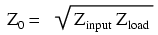


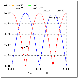


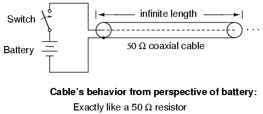


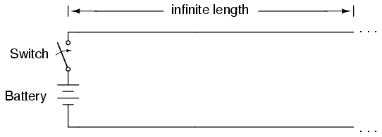
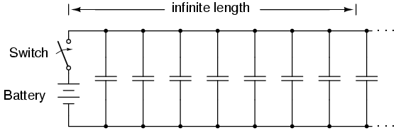
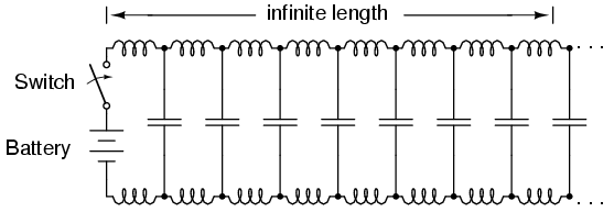
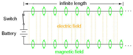
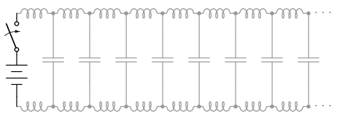
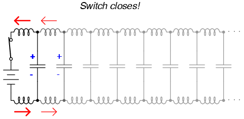
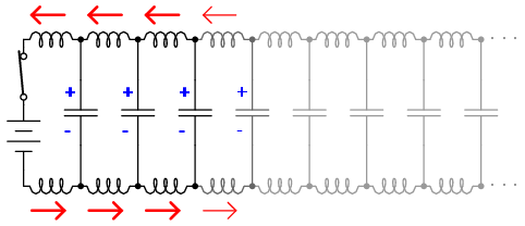
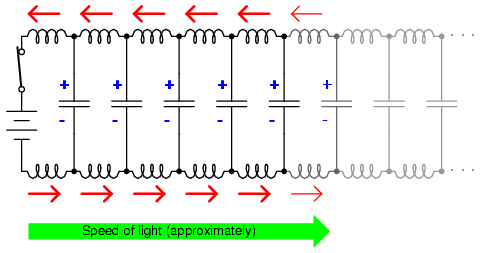
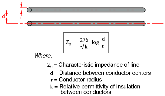
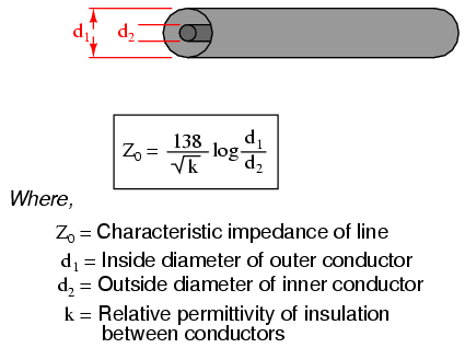
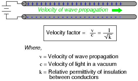
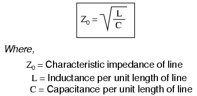
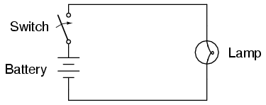


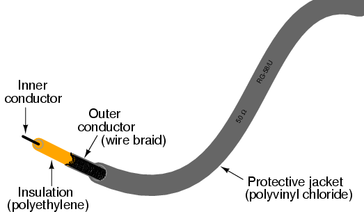


 B-field, view towards cross-section.
 B-field, view from the side.
 E-field, view towards cross-section.
.png)
.png)
.png)
 B-field, view towards cross-section.
 B-field, view from the side.
 E-field, view towards cross-section.
.png)
.png)
.png)
 TE1,1 mode of a circular hollow metallic waveguide.


![{\displaystyle t_{j}={\lambda \over 4n_{j}}(2N-1)[1-{n_{c}^{2} \over n_{j}^{2}}+{\lambda ^{2} \over 4n_{j}^{2}t_{c}^{2}}]^{-1/2},N=1,2,3,...}](https://wikimedia.org/api/rest_v1/media/math/render/svg/3f4f096ba8cab11c03a6a5270b32b069dcae0e5b)


 where c is the speed of light (≈3×10⁸ m·s−1).


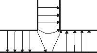
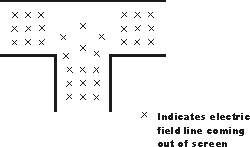
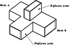
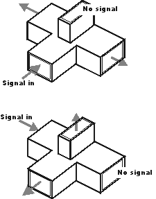


Awesome blog provides me great knowledge about waveguide components
BalasHapus