
The microwave domain
Microwave is a term used to identify electromagnetic waves above 103 megahertz (1 Gigahertz) up to 300 Gigahertz because of the short physical wavelengths of these frequencies. Short wavelength energy offers distinct advantages in many applications. For instance, sufficient directivity can be obtained using relatively small antennas and low-power transmitters. These characteristics are ideal for use in both military and civilian radar and communication applications. Small antennas and other small components are made possible by microwave frequency applications. The size advantage can be considered as part of a solution to problems of space, or weight, or both. Microwave frequency usage is significant for the design of shipboard radar because it makes possible the detection of smaller targets. Microwave frequencies present special problems in transmission, generation, and circuit design that are not encountered at lower frequencies. Conventional circuit theory is based on voltages and currents while microwave theory is based on electromagnetic fields.
Apparatus and techniques may be described qualitatively as "microwave" when the wavelengths of signals are roughly the same as the dimensions of the equipment, so that lumped-element circuit theory is inaccurate. As a consequence, practical microwave technique tends to move away from the discrete resistors, capacitors, and inductors used with lower frequency radio waves. Instead, distributed circuit elements and transmission-line theory are more useful methods for design and analysis. Open-wire and coaxial transmission lines give way to waveguides and stripline, and lumped-element tuned circuits are replaced by cavity resonators or resonant lines. Effects of reflection, polarization, scattering, diffraction and atmospheric absorption usually associated with visible light are of practical significance in the study of microwave propagation. The same equations of electromagnetic theory apply at all frequencies .
The microwave engineering discipline has become relevant as the microwave domain moves into the commercial sector, and no longer only applicable to 20th and 21st century military technologies. Inexpensive components and digital communications in the microwave domain have opened up areas pertinent to this discipline. Some of these areas are radar, satellite, wireless radio, optical communication, faster computer circuits, and collision avoidance radar .
Microwave transmission is the transmission of information or energy by microwave radio waves. Although an experimental 64 km (40 mile) microwave telecommunication link across the English Channel was demonstrated in 1931, the development of radar in World War II provided the technology for practical exploitation of microwave communication. In the 1950s, large transcontinental microwave relay networks, consisting of chains of repeater stations linked by line-of-sight beams of microwaves were built in Europe and America to relay long distance telephone traffic and television programs between cities. Communication satellites which transferred data between ground stations by microwaves took over much long distance traffic in the 1960s. In recent years, there has been an explosive increase in use of the microwave spectrum by new telecommunication technologies such as wireless networks, and direct-broadcast satellites which broadcast television and radio directly into consumers' homes.
The atmospheric attenuation of microwaves in dry air with a precipitable water vapor level of 0.001 mm. The downward spikes in the graph corresponds to frequencies at which microwaves are absorbed more strongly, such as by oxygen molecules .
Uses
Microwaves are widely used for point-to-point communications because their small wavelength allows conveniently-sized antennas to direct them in narrow beams, which can be pointed directly at the receiving antenna. This allows nearby microwave equipment to use the same frequencies without interfering with each other, as lower frequency radio waves do. Another advantage is that the high frequency of microwaves gives the microwave band a very large information-carrying capacity; the microwave band has a bandwidth 30 times that of all the rest of the radio spectrum below it. A disadvantage is that microwaves are limited to line of sight propagation; they cannot pass around hills or mountains as lower frequency radio waves can.Microwave radio transmission is commonly used in point-to-point communication systems on the surface of the Earth, in satellite communications, and in deep space radio communications. Other parts of the microwave radio band are used for radars, radio navigation systems, sensor systems, and radio astronomy.
The next higher part of the radio electromagnetic spectrum, where the frequencies are above 30 GHz and below 100 GHz, are called "millimeter waves" because their wavelengths are conveniently measured in millimeters, and their wavelengths range from 10 mm down to 3.0 mm (Higher frequency waves are smaller in wavelength). Radio waves in this band are usually strongly attenuated by the Earthly atmosphere and particles contained in it, especially during wet weather. Also, in wide band of frequencies around 60 GHz, the radio waves are strongly attenuated by molecular oxygen in the atmosphere. The electronic technologies needed in the millimeter wave band are also much more difficult to utilize than those of the microwave band.
- Wireless transmission of information
- One-way (e.g. television broadcasting) and two-way telecommunication using communications satellite
- Terrestrial microwave relay links in telecommunications networks including backbone or backhaul carriers in cellular networks


C band horn-reflector antennas on the roof of a telephone switching center in Seattle, Washington, part of the U.S. AT&T Long Lines microwave relay network.
- Wireless transmission of power
- Proposed systems e.g. for connecting solar power collecting satellites to terrestrial power grids
Microwave radio relay

Beginning in the 1950s, networks of microwave relay links, such as the AT&T Long Lines system in the U.S., carried long distance telephone calls and television programs between cities. The first system, dubbed TD-2 and built by AT&T, connected New York and Boston in 1947 with a series of eight radio relay stations.[1] These included long daisy-chained series of such links that traversed mountain ranges and spanned continents. Much of the transcontinental traffic is now carried by cheaper optical fibers and communication satellites, but microwave relay remains important for shorter distances.
Planning

Because of the high frequencies used, a line-of-sight path between the stations is required. Additionally, in order to avoid attenuation of the beam an area around the beam called the first Fresnel zone must be free from obstacles. Obstacles in the signal field cause unwanted attenuation. High mountain peak or ridge positions are often ideal


Production truck used for remote broadcasts by television news has a microwave dish on a retractible telescoping mast to transmit live video back to the studio.
The effects of atmospheric stratification cause the radio path to bend downward in a typical situation so a major distance is possible as the earth equivalent curvature increases from 6370 km to about 8500 km (a 4/3 equivalent radius effect). Rare events of temperature, humidity and pressure profile versus height, may produce large deviations and distortion of the propagation and affect transmission quality. High intensity rain and snow making rain fade must also be considered as an impairment factor, especially at frequencies above 10 GHz. All previous factors, collectively known as path loss, make it necessary to compute suitable power margins, in order to maintain the link operative for a high percentage of time, like the standard 99.99% or 99.999% used in 'carrier class' services of most telecommunication operators.
The link was built in 1979 by Telettra to transmit 300 telephone channels and 1 TV signal, in the 2 GHz frequency band. (Hop distance is the distance between two microwave stations) .
Previous considerations represent typical problems characterizing terrestrial radio links using microwaves for the so-called backbone networks: hop lengths of few tens of kilometers (typically 10 to 60 km) were largely used until 1990s. Frequency bands below 10 GHz and, above all, the information to be transmitted was a stream containing a fixed capacity block. The target was to supply the requested availability for the whole block (Plesiochronous digital hierarchy, PDH, or Synchronous Digital Hierarchy, SDH). Fading and/or multipath affecting the link for short time period during the day had to be counteracted by the diversity architecture. During 1990s microwave radio links begun widely to be used for urban links in cellular network. Requirements regarding link distances changed to shorter hops (less than 10 km, typically 3 to 5 km) and frequency increased to bands between 11 and 43 GHz and more recently up to 86 GHz (E-band). Furthermore, link planning deals more with intense rainfall and less with multipath, so diversity schemes became less used. Another big change that occurred during the last decade was evolution towards packet radio transmission. Therefore, new countermeasures, such as adaptive modulation, have been adopted.
The emitted power is regulated by norms (EIRP) both for cellular system and microwave. These microwave transmissions use emitted power typically from 30 mW to 0,3 W, radiated by the parabolic antenna on a beam wide round few degrees (1 to 3-4). The microwave channel arrangement is regulated by International Telecommunication Union (ITU-R) or local regulations (ETSI, FCC). In the last decade the dedicated spectrum for each microwave band reaches an extreme overcrowding, forcing efforts towards techniques for increasing the transmission capacity (frequency reuse, Polarization-division multiplexing, XPIC, MIMO).
Flash Back


US Army Signal Corps portable microwave relay station, 1945. Microwave relay systems were first developed in World War 2 for secure military communication
In 1931 an Anglo-French consortium headed by Andre C. Clavier demonstrated an experimental microwave relay link across the English Channel using 10 foot (3 m) dishes. Telephony, telegraph and facsimile data was transmitted over the bidirectional 1.7 GHz beams 64 km (40 miles) between Dover, UK and Calais, France. The radiated power, produced by a miniature Barkhausen-Kurz tube located at the dish's focus, was one-half watt. A 1933 military microwave link between airports at St. Inglevert, UK and Lympne, France, a distance of 56 km (35 miles) was followed in 1935 by a 300 MHz telecommunication link, the first commercial microwave relay system.
The development of radar during World War II provided much of the microwave technology which made practical microwave communication links possible, particularly the klystron oscillator and techniques of designing parabolic antennas. Though not commonly known, the US military used both portable and fixed-station microwave communications in the European Theater during World War II.
After the war telephone companies used this technology to build large microwave radio relay networks to carry long distance telephone calls. During the 1950s a unit of the US telephone carrier, AT&T Long Lines, built a transcontinental system of microwave relay links across the US that grew to carry the majority of US long distance telephone traffic, as well as television network signals. The main motivation in 1946 to use microwave radio instead of cable was that a large capacity could be installed quickly and at less cost. It was expected at that time that the annual operating costs for microwave radio would be greater than for cable. There were two main reasons that a large capacity had to be introduced suddenly: Pent up demand for long distance telephone service, because of the hiatus during the war years, and the new medium of television, which needed more bandwidth than radio. The prototype was called TDX and was tested with a connection between New York City and Murray Hill, the location of Bell Laboratories in 1946. The TDX system was set up between New York and Boston in 1947. The TDX was upgraded to the TD2 system, which used [the Morton tube, 416B and later 416C, manufactured by Western Electric] in the transmitters, and then later to TD3 that used solid state electronics.
Military microwave relay systems continued to be used into the 1960s, when many of these systems were supplanted with tropospheric scatter or communication satellite systems. When the NATO military arm was formed, much of this existing equipment was transferred to communications groups. The typical communications systems used by NATO during that time period consisted of the technologies which had been developed for use by the telephone carrier entities in host countries. One example from the USA is the RCA CW-20A 1–2 GHz microwave relay system which utilized flexible UHF cable rather than the rigid waveguide required by higher frequency systems, making it ideal for tactical applications. The typical microwave relay installation or portable van had two radio systems (plus backup) connecting two line of sight sites. These radios would often carry 24 telephone channels frequency division multiplexed on the microwave carrier (i.e. Lenkurt 33C FDM). Any channel could be designated to carry up to 18 teletype communications instead. Similar systems from Germany and other member nations were also in use.
Long distance microwave relay networks were built in many countries until the 1980s, when the technology lost its share of fixed operation to newer technologies such as fiber-optic cable and communication satellites, which offer lower cost per bit.
During the Cold War, the US intelligence agencies, such as the National Security Agency (NSA), were reportedly able to intercept Soviet microwave traffic using satellites such as Rhyolite.[8] Much of the beam of a microwave link passes the receiving antenna and radiates toward the horizon, into space. By positioning a geosynchronous satellite in the path of the beam, the microwave beam can be received.

At the turn of the century, microwave radio relay systems are being used increasingly in portable radio applications. The technology is particularly suited to this application because of lower operating costs, a more efficient infrastructure, and provision of direct hardware access to the portable radio operator.
A microwave link is a communications system that uses a beam of radio waves in the microwave frequency range to transmit video, audio, or data between two locations, which can be from just a few feet or meters to several miles or kilometers apart. Microwave links are commonly used by television broadcasters to transmit programmes across a country, for instance, or from an outside broadcast back to a studio.
Mobile units can be camera mounted, allowing cameras the freedom to move around without trailing cables. These are often seen on the touchlines of sports fields on Steadicam systems.
Properties of microwave links
- Involve line of sight (LOS) communication technology
- Affected greatly by environmental constraints, including rain fade
- Have very limited penetration capabilities through obstacles such as hills, buildings and trees
- Sensitive to high pollen count
- Signals can be degraded during Solar proton events
Uses of microwave links
- In communications between satellites and base stations
- As backbone carriers for cellular systems
- In short range indoor communications
- Linking remote and regional telephone exchanges to larger (main) exchanges without the need for copper/optical fibre lines.
- Measuring the intensity of rain between two locations
Troposcatter
Terrestrial microwave relay links are limited in distance to the visual horizon, a few tens of miles or kilometers depending on tower height. Tropospheric scatter ("troposcatter" or "scatter") was a technology developed in the 1950s allow microwave communication links beyond the horizon, to a range of several hundred kilometers. The transmitter radiates a beam of microwaves into the sky, at a shallow angle above the horizon toward the receiver. As the beam passes through the troposphere a small fraction of the microwave energy is scattered back toward the ground by water vapor and dust in the air. A sensitive receiver beyond the horizon picks up this reflected signal. Signal clarity obtained by this method depends on the weather and other factors, and as a result a high level of technical difficulty is involved in the creation of a reliable over horizon radio relay link. Troposcatter links are therefore only used in special circumstances where satellites and other long distance communication channels cannot be relied on, such as in military communications.Microwave power transmission
Microwave power transmission (MPT) is the use of microwaves to transmit power through outer space or the atmosphere without the need for wires. It is a sub-type of the more general wireless energy transfer methods.Flash Back
Following World War II, which saw the development of high-power microwave emitters known as cavity magnetrons, the idea of using microwaves to transmit power was researched. In 1964, William C. Brown demonstrated a miniature helicopter equipped with a combination antenna and rectifier device called a rectenna. The rectenna converted microwave power into electricity, allowing the helicopter to fly.[10] In principle, the rectenna is capable of very high conversion efficiencies - over 90% in optimal circumstances.Most proposed MPT systems now usually include a phased array microwave transmitter. While these have lower efficiency levels, they have the advantage of being electrically steered using no moving parts, and are easier to scale to the necessary levels that a practical MPT system requires.
Using microwave power transmission to deliver electricity to communities without having to build cable-based infrastructure is being studied at Grand Bassin on Reunion Island in the Indian Ocean.
Common safety concerns
The common reaction to microwave transmission is one of concern, as microwaves are generally perceived by the public as dangerous forms of radiation, stemming from the fact that they are used in microwave ovens. While high power microwaves can be painful and dangerous as in the United States Military's Active Denial System, MPT systems are generally proposed to have only low intensity at the rectenna.Though this would be extremely safe as the power levels would be about equal to the leakage from a microwave oven, and only slightly more than a cell phone, the relatively diffuse microwave beam necessitates a large receiving antenna area for a significant amount of energy to be transmitted.
Research has involved exposing multiple generations of animals to microwave radiation of this or higher intensity, and no health issues have been found.
Proposed uses
MPT is the most commonly proposed method for transferring energy to the surface of the Earth from solar power satellites or other in-orbit power sources. MPT is occasionally proposed for the power supply in beam-powered propulsion for orbital lift space ships. Even though lasers are more commonly proposed, their low efficiency in light generation and reception has led some designers to opt for microwave based systems.Current status
Wireless power transmission (using microwaves) is well proven. Experiments in the tens of kilowatts have been performed at Goldstone in California in 1975 and more recently (1997) at Grand Bassin on Reunion Island. In 2008, a long-range transmission experiment successfully transmitted 20 watts 92 miles (148 km) from a mountain on Maui to the main island of Hawaii.JAXA announced on 12 March 2015 that they wirelessly beamed 1.8 kilowatts 50 meters to a small receiver by converting electricity to microwaves and then back to electricity. This is the standard plan for this type of power. On 12 March 2015, Mitsubishi Heavy Industries demonstrated transmission of 10 kilowatts (kW) of power to a receiver unit located at a distance of 500 meters (m) away
XXX . XXX Wireless power transfer
Wireless power transfer (WPT), wireless power transmission, wireless energy transmission, or electromagnetic power transfer is the transmission of electrical energy without wires. Wireless power transmission technologies use time-varying electric, magnetic, or electromagnetic fields. Wireless transmission is useful to power electrical devices where interconnecting wires are inconvenient, hazardous, or are not possible.
Wireless power techniques mainly fall into two categories, non-radiative and radiative. In near field or non-radiative techniques, power is transferred over short distances by magnetic fields using inductive coupling between coils of wire, or by electric fields using capacitive coupling between metal electrodes. Inductive coupling is the most widely used wireless technology; its applications include charging handheld devices like phones and electric toothbrushes, RFID tags, and chargers for implantable medical devices like artificial cardiac pacemakers, or electric vehicles.
In far-field or radiative techniques, also called power beaming, power is transferred by beams of electromagnetic radiation, like microwaves or laser beams. These techniques can transport energy longer distances but must be aimed at the receiver. Proposed applications for this type are solar power satellites, and wireless powered drone aircraft.
An important issue associated with all wireless power systems is limiting the exposure of people and other living things to potentially injurious electromagnetic fields
.jpg)
Inductive charging pad for LG smartphone, using the Qi system, an example of near-field wireless transfer. When the phone is set on the pad, a coil in the pad creates a magnetic field[1] which induces a current in another coil, in the phone, charging its battery.
Overview
Coupling (electronics)
Wireless power transfer is a generic term for a number of different technologies for transmitting energy by means of electromagnetic fields.[8][9][10] The technologies, listed in the table below, differ in the distance over which they can transfer power efficiently, whether the transmitter must be aimed (directed) at the receiver, and in the type of electromagnetic energy they use: time varying electric fields, magnetic fields, radio waves, microwaves, infrared or visible light waves.[11]
In general a wireless power system consists of a "transmitter" connected to a source of power such as a mains power line, which converts the power to a time-varying electromagnetic field, and one or more "receiver" devices which receive the power and convert it back to DC or AC electric current which is used by an electrical load.[8][11] At the transmitter the input power is converted to an oscillating electromagnetic field by some type of "antenna" device. The word "antenna" is used loosely here; it may be a coil of wire which generates a magnetic field, a metal plate which generates an electric field, an antenna which radiates radio waves, or a laser which generates light. A similar antenna or coupling device at the receiver converts the oscillating fields to an electric current. An important parameter that determines the type of waves is the frequency, which determines the wavelength.
Wireless power uses the same fields and waves as wireless communication devices like radio, another familiar technology that involves electrical energy transmitted without wires by electromagnetic fields, used in cellphones, radio and television broadcasting, and WiFi. In radio communication the goal is the transmission of information, so the amount of power reaching the receiver is not so important, as long as it is sufficient that the information can be received intelligibly In wireless communication technologies only tiny amounts of power reach the receiver. In contrast, with wireless power the amount of energy received is the important thing, so the efficiency (fraction of transmitted energy that is received) is the more significant parameter.[9] For this reason, wireless power technologies are likely to be more limited by distance than wireless communication technologies.
These are the different wireless power technologies:[
| Technology | Range[17] | Directivity[11] | Frequency | Antenna devices | Current and/or possible future applications |
|---|---|---|---|---|---|
| Inductive coupling | Short | Low | Hz – MHz | Wire coils | Electric tooth brush and razor battery charging, induction stovetops and industrial heaters. |
| Resonant inductive coupling | Mid- | Low | kHz – GHz | Tuned wire coils, lumped element resonators | Charging portable devices (Qi), biomedical implants, electric vehicles, powering buses, trains, MAGLEV, RFID, smartcards. |
| Capacitive coupling | Short | Low | kHz – MHz | Metal plate electrodes | Charging portable devices, power routing in large-scale integrated circuits, Smartcards. |
| Magnetodynamic coupling[15] | Short | N.A. | Hz | Rotating magnets | Charging electric vehicles, buses, biomedical implants. |
| Microwaves | Long | High | GHz | Parabolic dishes, phased arrays, rectennas | Solar power satellite, powering drone aircraft, charging wireless devices |
| Light waves | Long | High | ≥THz | Lasers, photocells, lenses | Powering drone aircraft, powering space elevator climbers. |
Field regions
Electric and magnetic fields are created by charged particles in matter such as electrons. A stationary charge creates an electrostatic field in the space around it. A steady current of charges (direct current, DC) creates a static magnetic field around it. The above fields contain energy, but cannot carry power because they are static. However time-varying fields can carry power.[18] Accelerating electric charges, such as are found in an alternating current (AC) of electrons in a wire, create time-varying electric and magnetic fields in the space around them. These fields can exert oscillating forces on the electrons in a receiving "antenna", causing them to move back and forth. These represent alternating current which can be used to power a load.The oscillating electric and magnetic fields surrounding moving electric charges in an antenna device can be divided into two regions, depending on distance Drange from the antenna The boundary between the regions is somewhat vaguely defined.[11] The fields have different characteristics in these regions, and different technologies are used for transferring power:
- Near-field or nonradiative region – This means the area within about 1 wavelength (λ) of the antenna.[ In this region the oscillating electric and magnetic fields are separate[12] and power can be transferred via electric fields by capacitive coupling (electrostatic induction) between metal electrodes, or via magnetic fields by inductive coupling (electromagnetic induction) between coils of wire.[ These fields are not radiative,[20] meaning the energy stays within a short distance of the transmitter. If there is no receiving device or absorbing material within their limited range to "couple" to, no power leaves the transmitter.[22] The range of these fields is short, and depends on the size and shape of the "antenna" devices, which are usually coils of wire. The fields, and thus the power transmitted, decrease exponentially with distance,[ so if the distance between the two "antennas" Drange is much larger than the diameter of the "antennas" Dant very little power will be received. Therefore, these techniques cannot be used for long range power transmission.
- Resonance, such as resonant inductive coupling, can increase the coupling between the antennas greatly, allowing efficient transmission at somewhat greater distances, although the fields still decrease exponentially. Therefore the range of near-field devices is conventionally divided into two categories:
- Short range – up to about one antenna diameter: Drange ≤ Dant. This is the range over which ordinary nonresonant capacitive or inductive coupling can transfer practical amounts of power.
- Mid-range – up to 10 times the antenna diameter: Drange ≤ 10 Dant.[ This is the range over which resonant capacitive or inductive coupling can transfer practical amounts of power.
- Far-field or radiative region – Beyond about 1 wavelength (λ) of the antenna, the electric and magnetic fields are perpendicular to each other and propagate as an electromagnetic wave; examples are radio waves, microwaves, or light waves.[ This part of the energy is radiative,[20] meaning it leaves the antenna whether or not there is a receiver to absorb it. The portion of energy which does not strike the receiving antenna is dissipated and lost to the system. The amount of power emitted as electromagnetic waves by an antenna depends on the ratio of the antenna's size Dant to the wavelength of the waves λ,[28] which is determined by the frequency: λ = c/f. At low frequencies f where the antenna is much smaller than the size of the waves, Dant << λ, very little power is radiated. Therefore the near-field devices above, which use lower frequencies, radiate almost none of their energy as electromagnetic radiation. Antennas about the same size as the wavelength Dant ≈ λ such as monopole or dipole antennas, radiate power efficiently, but the electromagnetic waves are radiated in all directions (omnidirectionally), so if the receiving antenna is far away, only a small amount of the radiation will hit it. Therefore, these can be used for short range, inefficient power transmission but not for long range transmission.[29]
- However, unlike fields, electromagnetic radiation can be focused by reflection or refraction into beams. By using a high-gain antenna or optical system which concentrates the radiation into a narrow beam aimed at the receiver, it can be used for long range power transmission. From the Rayleigh criterion, to produce the narrow beams necessary to focus a significant amount of the energy on a distant receiver, an antenna must be much larger than the wavelength of the waves used: Dant >> λ = c/f.[30] Practical beam power devices require wavelengths in the centimeter region or below, corresponding to frequencies above 1 GHz, in the microwave range or above.[8]
Near-field (nonradiative) techniques
At large relative distance, the near-field components of electric and magnetic fields are approximately quasi-static oscillating dipole fields. These fields decrease with the cube of distance: (Drange/Dant)−3 Since power is proportional to the square of the field strength, the power transferred decreases as (Drange/Dant)−6.[ or 60 dB per decade. In other words, if far apart, doubling the distance between the two antennas causes the power received to decrease by a factor of 26 = 64. As a result, inductive and capacitive coupling can only be used for short-range power transfer, within a few times the diameter of the antenna device Dant. Unlike in a radiative system where the maximum radiation occurs when the dipole antennas are oriented transverse to the direction of propagation, with dipole fields the maximum coupling occurs when the dipoles are oriented longitudinally.Inductive coupling


(left) Modern inductive power transfer, an electric toothbrush charger. A coil in the stand produces a magnetic field, inducing an alternating current in a coil in the toothbrush, which is rectified to charge the batteries.
(right) A light bulb powered wirelessly by induction, in 1910.
(right) A light bulb powered wirelessly by induction, in 1910.
Inductive coupling is the oldest and most widely used wireless power technology, and virtually the only one so far which is used in commercial products. It is used in inductive charging stands for cordless appliances used in wet environments such as electric toothbrushes[14] and shavers, to reduce the risk of electric shock.[35] Another application area is "transcutaneous" recharging of biomedical prosthetic devices implanted in the human body, such as cardiac pacemakers and insulin pumps, to avoid having wires passing through the skin.[36][37] It is also used to charge electric vehicles such as cars and to either charge or power transit vehicles like buses and trains.[14][16]
However the fastest growing use is wireless charging pads to recharge mobile and handheld wireless devices such as laptop and tablet computers, cellphones, digital media players, and video game controllers.[16]
The power transferred increases with frequency[34] and the mutual inductance between the coils,[9] which depends on their geometry and the distance between them. A widely used figure of merit is the coupling coefficient . This dimensionless parameter is equal to the fraction of magnetic flux through the transmitter coil that passes through the receiver coil when L2 is open circuited. If the two coils are on the same axis and close together so all the magnetic flux from passes through , and the link efficiency approaches 100%. The greater the separation between the coils, the more of the magnetic field from the first coil misses the second, and the lower and the link efficiency are, approaching zero at large separations.[34] The link efficiency and power transferred is roughly proportional to .[34] In order to achieve high efficiency, the coils must be very close together, a fraction of the coil diameter ,[34] usually within centimeters,[29] with the coils' axes aligned. Wide, flat coil shapes are usually used, to increase coupling.[34] Ferrite "flux confinement" cores can confine the magnetic fields, improving coupling and reducing interference to nearby electronics,[ but they are heavy and bulky so small wireless devices often use air-core coils.


Ordinary inductive coupling can only achieve high efficiency when the coils are very close together, usually adjacent. In most modern inductive systems resonant inductive coupling (described below) is used, in which the efficiency is increased by using resonant circuits. This can achieve high efficiencies at greater distances than nonresonant inductive coupling.

Prototype inductive electric car charging system at 2011 Tokyo Auto Show

Powermat inductive charging spots in a coffee shop. Customers can set their phones and computers on them to recharge.

Wireless powered access card.
Resonant inductive coupling
Tesla coil § Resonant transformer

Diagram of the resonant inductive wireless power system demonstrated by Marin Soljačić's MIT team in 2007. The resonant circuits were coils of copper wire which resonated with their internal capacitance (dotted capacitors) at 10 MHz. Power was coupled into the transmitter resonator, and out of the receiver resonator into the rectifier, by small coils which also served for impedance matching.
Nikola Tesla first discovered resonant coupling during his pioneering experiments in wireless power transfer around the turn of the 20th century,[ but the possibilities of using resonant coupling to increase transmission range has only recently been explored.[43] In 2007 a team led by Marin Soljačić at MIT used two coupled tuned circuits each made of a 25 cm self-resonant coil of wire at 10 MHz to achieve the transmission of 60 W of power over a distance of 2 meters (6.6 ft) (8 times the coil diameter) at around 40% efficiency . Soljačić founded the company WiTricity (the same name the team used for the technology) which is attempting to commercialize the technology.
The concept behind the WiTricity resonant inductive coupling system is that high Q factor resonators (Highly Resonant) exchange energy at a much higher rate than they lose energy due to internal damping.[24] Therefore, by using resonance, the same amount of power can be transferred at greater distances, using the much weaker magnetic fields out in the peripheral regions ("tails") of the near fields (these are sometimes called evanescent fields[24]). Resonant inductive coupling can achieve high efficiency at ranges of 4 to 10 times the coil diameter (Dant). This is called "mid-range" transfer,[26] in contrast to the "short range" of nonresonant inductive transfer, which can achieve similar efficiencies only when the coils are adjacent. Another advantage is that resonant circuits interact with each other so much more strongly than they do with nonresonant objects that power losses due to absorption in stray nearby objects are negligible.
A drawback of resonant coupling theory is that at close ranges when the two resonant circuits are tightly coupled, the resonant frequency of the system is no longer constant but "splits" into two resonant peaks,[ so the maximum power transfer no longer occurs at the original resonant frequency and the oscillator frequency must be tuned to the new resonance peak. The case of using such a shifted peak is called "Single resonant".[49] The "Single resonant" systems have also been used, in which only the secondary is a tuned circuit. The principle of this phenomenon is also called "(Magnetic) phase synchronization" and already started practical application for AGV in Japan from around 1993.[53] And now, the concept of Highly Resonant presented by researcher of MIT is applied only to the secondary side resonator, and high efficiency wide gap high power wireless power transfer system is realized and it is used for induction current collector of SCMaglev.
Resonant technology is currently being widely incorporated in modern inductive wireless power systems.[34] One of the possibilities envisioned for this technology is area wireless power coverage. A coil in the wall or ceiling of a room might be able to wirelessly power lights and mobile devices anywhere in the room, with reasonable efficiency.[35] An environmental and economic benefit of wirelessly powering small devices such as clocks, radios, music players and remote controls is that it could drastically reduce the 6 billion batteries disposed of each year, a large source of toxic waste and groundwater contamination.
Capacitive coupling
In capacitive coupling (electrostatic induction), the conjugate of inductive coupling, energy is transmitted by electric fields[9] between electrodes such as metal plates. The transmitter and receiver electrodes form a capacitor, with the intervening space as the dielectric.[9][12][14][36][55] An alternating voltage generated by the transmitter is applied to the transmitting plate, and the oscillating electric field induces an alternating potential on the receiver plate by electrostatic induction,[9][55] which causes an alternating current to flow in the load circuit. The amount of power transferred increases with the frequency[55] the square of the voltage, and the capacitance between the plates, which is proportional to the area of the smaller plate and (for short distances) inversely proportional to the separation.[9]
Capacitive wireless power systems

Bipolar coupling

Unipolar coupling
Two types of circuit have been used:
- Bipolar design: In this type of circuit, there are two transmitter plates and two receiver plates. Each transmitter plate is coupled to a receiver plate. The transmitter oscillator drives the transmitter plates in opposite phase (180° phase difference) by a high alternating voltage, and the load is connected between the two receiver plates. The alternating electric fields induce opposite phase alternating potentials in the receiver plates, and this "push-pull" action causes current to flow back and forth between the plates through the load. A disadvantage of this configuration for wireless charging is that the two plates in the receiving device must be aligned face to face with the charger plates for the device to work.
- Unipolar design: In this type of circuit, the transmitter and receiver have only one active electrode, and either the ground or a large passive electrode serves as the return path for the current. The transmitter oscillator is connected between an active and a passive electrode. The load is also connected between an active and a passive electrode. The electric field produced by the transmitter induces alternating charge displacement in the load dipole through electrostatic induction.
Resonant capacitive coupling
Resonance can also be used with capacitive coupling to extend the range. At the turn of the 20th century, Nikola Tesla did the first experiments with both resonant inductive and capacitive coupling.Magnetodynamic coupling
In this method, power is transmitted between two rotating armatures, one in the transmitter and one in the receiver, which rotate synchronously, coupled together by a magnetic field generated by permanent magnets on the armatures.[15] The transmitter armature is turned either by or as the rotor of an electric motor, and its magnetic field exerts torque on the receiver armature, turning it. The magnetic field acts like a mechanical coupling between the armatures.[15] The receiver armature produces power to drive the load, either by turning a separate electric generator or by using the receiver armature itself as the rotor in a generator.This device has been proposed as an alternative to inductive power transfer for noncontact charging of electric vehicles.[15] A rotating armature embedded in a garage floor or curb would turn a receiver armature in the underside of the vehicle to charge its batteries.[15] It is claimed that this technique can transfer power over distances of 10 to 15 cm (4 to 6 inches) with high efficiency, over 90%. Also, the low frequency stray magnetic fields produced by the rotating magnets produce less electromagnetic interference to nearby electronic devices than the high frequency magnetic fields produced by inductive coupling systems. A prototype system charging electric vehicles has been in operation at University of British Columbia since 2012. Other researchers, however, claim that the two energy conversions (electrical to mechanical to electrical again) make the system less efficient than electrical systems like inductive coupling.
Far-field (radiative) techniques
Far field methods achieve longer ranges, often multiple kilometer ranges, where the distance is much greater than the diameter of the device(s). The main reason for longer ranges with radio wave and optical devices is the fact that electromagnetic radiation in the far-field can be made to match the shape of the receiving area (using high directivity antennas or well-collimated laser beams). The maximum directivity for antennas is physically limited by diffraction.In general, visible light (from lasers) and microwaves (from purpose-designed antennas) are the forms of electromagnetic radiation best suited to energy transfer.
The dimensions of the components may be dictated by the distance from transmitter to receiver, the wavelength and the Rayleigh criterion or diffraction limit, used in standard radio frequency antenna design, which also applies to lasers. Airy's diffraction limit is also frequently used to determine an approximate spot size at an arbitrary distance from the aperture. Electromagnetic radiation experiences less diffraction at shorter wavelengths (higher frequencies); so, for example, a blue laser is diffracted less than a red one.
The Rayleigh criterion dictates that any radio wave, microwave or laser beam will spread and become weaker and diffuse over distance; the larger the transmitter antenna or laser aperture compared to the wavelength of radiation, the tighter the beam and the less it will spread as a function of distance (and vice versa). Smaller antennae also suffer from excessive losses due to side lobes. However, the concept of laser aperture considerably differs from an antenna. Typically, a laser aperture much larger than the wavelength induces multi-moded radiation and mostly collimators are used before emitted radiation couples into a fiber or into space.
Ultimately, beamwidth is physically determined by diffraction due to the dish size in relation to the wavelength of the electromagnetic radiation used to make the beam.
Microwave power beaming can be more efficient than lasers, and is less prone to atmospheric attenuation caused by dust or water vapor.
Here, the power levels are calculated by combining the above parameters together, and adding in the gains and losses due to the antenna characteristics and the transparency and dispersion of the medium through which the radiation passes. That process is known as calculating a link budget.
Microwaves

An artist's depiction of a solar satellite that could send electric energy by microwaves to a space vessel or planetary surface.
Power beaming by microwaves has the difficulty that, for most space applications, the required aperture sizes are very large due to diffraction limiting antenna directionality. For example, the 1978 NASA study of solar power satellites required a 1-kilometre-diameter (0.62 mi) transmitting antenna and a 10-kilometre-diameter (6.2 mi) receiving rectenna for a microwave beam at 2.45 GHz.[65] These sizes can be somewhat decreased by using shorter wavelengths, although short wavelengths may have difficulties with atmospheric absorption and beam blockage by rain or water droplets. Because of the "thinned-array curse", it is not possible to make a narrower beam by combining the beams of several smaller satellites.
For earthbound applications, a large-area 10 km diameter receiving array allows large total power levels to be used while operating at the low power density suggested for human electromagnetic exposure safety. A human safe power density of 1 mW/cm2 distributed across a 10 km diameter area corresponds to 750 megawatts total power level. This is the power level found in many modern electric power plants.
Following World War II, which saw the development of high-power microwave emitters known as cavity magnetrons, the idea of using microwaves to transfer power was researched. By 1964, a miniature helicopter propelled by microwave power had been demonstrated.[66]
Japanese researcher Hidetsugu Yagi also investigated wireless energy transmission using a directional array antenna that he designed. In February 1926, Yagi and his colleague Shintaro Uda published their first paper on the tuned high-gain directional array now known as the Yagi antenna. While it did not prove to be particularly useful for power transmission, this beam antenna has been widely adopted throughout the broadcasting and wireless telecommunications industries due to its excellent performance characteristics.[67]
Wireless high power transmission using microwaves is well proven. Experiments in the tens of kilowatts have been performed at Goldstone in California in 1975 and more recently (1997) at Grand Bassin on Reunion Island.[71] These methods achieve distances on the order of a kilometer.
Under experimental conditions, microwave conversion efficiency was measured to be around 54%.[72]
A change to 24 GHz has been suggested as microwave emitters similar to LEDs have been made with very high quantum efficiencies using negative resistance, i.e., Gunn or IMPATT diodes, and this would be viable for short range links.
In 2013, inventor Hatem Zeine demonstrated how wireless power transmission using phased array antennas can deliver electrical power up to 30 feet. It uses the same radio frequencies as WiFi.[73][74]
In 2015, researchers at the University of Washington introduced power over Wi-Fi, which trickle-charges batteries and powered battery-free cameras and temperature sensors using transmissions from Wi-Fi routers. Wi-Fi signals were shown to power battery-free temperature and camera sensors at ranges of up to 20 feet. It was also shown that Wi-Fi can be used to wirelessly trickle-charge nickel–metal hydride and lithium-ion coin-cell batteries at distances of up to 28 feet.
In 2017, the Federal Communication Commission (FCC) certified the first mid-field radio frequency (RF) transmitter of wireless power.
Lasers

Advantages compared to other wireless methods are:[81]
- Collimated monochromatic wavefront propagation allows narrow beam cross-section area for transmission over large distances.
- Compact size: solid state lasers fit into small products.
- No radio-frequency interference to existing radio communication such as Wi-Fi and cell phones.
- Access control: only receivers hit by the laser receive power.
- Laser radiation is hazardous. Low power levels can blind humans and other animals. High power levels can kill through localized spot heating.
- Conversion between electricity and light is limited. Photovoltaic cells achieve 40%–50% efficiency.[82] (The conversion efficiency of laser light into electricity is much higher than that of sun light into electricity).
- Atmospheric absorption, and absorption and scattering by clouds, fog, rain, etc., causes up to 100% losses.
- Requires a direct line of sight with the target. (Instead of being beamed directly onto the receiver, the laser light can also be guided by an optical fiber. Then one speaks of power-over-fiber technology.)
Other details include propagation,[88] and the coherence and the range limitation problem.[89]
Geoffrey Landis is one of the pioneers of solar power satellites[93] and laser-based transfer of energy especially for space and lunar missions. The demand for safe and frequent space missions has resulted in proposals for a laser-powered space elevator.[94][95]
NASA's Dryden Flight Research Center demonstrated a lightweight unmanned model plane powered by a laser beam.[96] This proof-of-concept demonstrates the feasibility of periodic recharging using the laser beam system.
Atmospheric plasma channel coupling
In atmospheric plasma channel coupling, energy is transferred between two electrodes by electrical conduction through ionized air.[97] When an electric field gradient exists between the two electrodes, exceeding 34 kilovolts per centimeter at sea level atmospheric pressure, an electric arc occurs. This atmospheric dielectric breakdown results in the flow of electric current along a random trajectory through an ionized plasma channel between the two electrodes. An example of this is natural lightning, where one electrode is a virtual point in a cloud and the other is a point on Earth. Laser Induced Plasma Channel (LIPC) research is presently underway using ultrafast lasers to artificially promote development of the plasma channel through the air, directing the electric arc, and guiding the current across a specific path in a controllable manner.[99] The laser energy reduces the atmospheric dielectric breakdown voltage and the air is made less insulating by superheating, which lowers the density () of the filament of air.[100]
This new process is being explored for use as a laser lightning rod and as a means to trigger lightning bolts from clouds for natural lightning channel studies,[101] for artificial atmospheric propagation studies, as a substitute for conventional radio antennas,[102] for applications associated with electric welding and machining, for diverting power from high-voltage capacitor discharges, for directed-energy weapon applications employing electrical conduction through a ground return path and electronic jamming.
Energy harvesting
In the context of wireless power, energy harvesting, also called power harvesting or energy scavenging, is the conversion of ambient energy from the environment to electric power, mainly to power small autonomous wireless electronic devices.[110] The ambient energy may come from stray electric or magnetic fields or radio waves from nearby electrical equipment, light, thermal energy (heat), or kinetic energy such as vibration or motion of the device.[110] Although the efficiency of conversion is usually low and the power gathered often minuscule (milliwatts or microwatts),[110] it can be adequate to run or recharge small micropower wireless devices such as remote sensors, which are proliferating in many fields.[111][110] This new technology is being developed to eliminate the need for battery replacement or charging of such wireless devices, allowing them to operate completely autonomouslyFlash Back
19th century developments and dead ends
The 19th century saw many developments of theories, and counter-theories on how electrical energy might be transmitted. In 1826 André-Marie Ampère found Ampère's circuital law showing that electric current produces a magnetic field. Michael Faraday described in 1831 with his law of induction the electromotive force driving a current in a conductor loop by a time-varying magnetic flux. The fact that electrical energy could by transmitted at a distance without wires was actually observed by many inventors and experimenters,[ but lack of a coherent theory attributed these phenomena vaguely to electromagnetic induction.[117] A concise explanation of these phenomena would come from the 1860s Maxwell's equations by James Clerk Maxwell, establishing a theory that unified electricity and magnetism to electromagnetism, predicting the existence of electromagnetic waves as the "wireless" carrier of electromagnetic energy. Around 1884 John Henry Poynting defined the Poynting vector and gave Poynting's theorem, which describe the flow of power across an area within electromagnetic radiation and allow for a correct analysis of wireless power transfer systems. This was followed on by Heinrich Rudolf Hertz' 1888 validation of the theory, which included the evidence for radio waves.During the same period two schemes of wireless signaling were put forward by William Henry Ward (1871) and Mahlon Loomis (1872) that were based on the erroneous belief that there was an electrified atmospheric stratum accessible at low altitude. Both inventors' patents noted this layer connected with a return path using "Earth currents"' would allow for wireless telegraphy as well as supply power for the telegraph, doing away with artificial batteries, and could also be used for lighting, heat, and motive power.[ A more practical demonstration of wireless transmission via conduction came in Amos Dolbear's 1879 magneto electric telephone that used ground conduction to transmit over a distance of a quarter of a mile.
Tesla

Tesla demonstrating wireless transmission by "electrostatic induction" during an 1891 lecture at Columbia College. The two metal sheets are connected to a Tesla coil oscillator, which applies high-voltage radio frequency alternating current. An oscillating electric field between the sheets ionizes the low-pressure gas in the two long Geissler tubes in his hands, causing them to glow in a manner similar to neon tubes.


(left) Experiment in resonant inductive transfer by Tesla at Colorado Springs 1899. The coil is in resonance with Tesla's magnifying transmitter nearby, powering the light bulb at bottom. (right) Tesla's unsuccessful Wardenclyffe power station.
Near-field and non-radiative technologies
Inductive power transfer between nearby wire coils was the earliest wireless power technology to be developed, existing since the transformer was developed in the 1800s. Induction heating has been used since the early 1900s. With the advent of cordless devices, induction charging stands have been developed for appliances used in wet environments, like electric toothbrushes and electric razors, to eliminate the hazard of electric shock. One of the earliest proposed applications of inductive transfer was to power electric locomotives. In 1892 Maurice Hutin and Maurice Leblanc patented a wireless method of powering railroad trains using resonant coils inductively coupled to a track wire at 3 kHz. The first passive RFID (Radio Frequency Identification) technologies were invented by Mario Cardullo (1973) and Koelle et al. (1975) and by the 1990s were being used in proximity cards and contactless smartcards.The proliferation of portable wireless communication devices such as mobile phones, tablet, and laptop computers in recent decades is currently driving the development of mid-range wireless powering and charging technology to eliminate the need for these devices to be tethered to wall plugs during charging.[145] The Wireless Power Consortium was established in 2008 to develop interoperable standards across manufacturers. Its Qi inductive power standard published in August 2009 enables high efficiency charging and powering of portable devices of up to 5 watts over distances of 4 cm (1.6 inches). The wireless device is placed on a flat charger plate (which can be embedded in table tops at cafes, for example) and power is transferred from a flat coil in the charger to a similar one in the device.
In 2007, a team led by Marin Soljačić at MIT used a dual resonance transmitter with a 25 cm diameter secondary tuned to 10 MHz to transfer 60 W of power to a similar dual resonance receiver over a distance of 2 meters (6.6 ft) (eight times the transmitter coil diameter) at around 40% efficiency. In 2008 the team of Greg Leyh and Mike Kennan of Nevada Lightning Lab used a grounded dual resonance transmitter with a 57 cm diameter secondary tuned to 60 kHz and a similar grounded dual resonance receiver to transfer power through coupled electric fields with an earth return circuit over a distance of 12 meters (39 ft).
Microwaves and lasers
Before World War 2, little progress was made in wireless power transmission. Radio was developed for communication uses, but couldn't be used for power transmission due to the fact that the relatively low-frequency radio waves spread out in all directions and little energy reached the receiver. In radio communication, at the receiver, an amplifier intensifies a weak signal using energy from another source. For power transmission, efficient transmission required transmitters that could generate higher-frequency microwaves, which can be focused in narrow beams towards a receiver.The development of microwave technology during World War 2, such as the klystron and magnetron tubes and parabolic antennas made radiative (far-field) methods practical for the first time, and the first long-distance wireless power transmission was achieved in the 1960s by William C. Brown. In 1964 Brown invented the rectenna which could efficiently convert microwaves to DC power, and in 1964 demonstrated it with the first wireless-powered aircraft, a model helicopter powered by microwaves beamed from the ground. A major motivation for microwave research in the 1970s and 80s was to develop a solar power satellite. Conceived in 1968 by Peter Glaser, this would harvest energy from sunlight using solar cells and beam it down to Earth as microwaves to huge rectennas, which would convert it to electrical energy on the electric power grid. In landmark 1975 experiments as technical director of a JPL/Raytheon program, Brown demonstrated long-range transmission by beaming 475 W of microwave power to a rectenna a mile away, with a microwave to DC conversion efficiency of 54%. At NASA's Jet Propulsion Laboratory he and Robert Dickinson transmitted 30 kW DC output power across 1.5 km with 2.38 GHz microwaves from a 26 m dish to a 7.3 x 3.5 m rectenna array. The incident-RF to DC conversion efficiency of the rectenna was 80%. In 1983 Japan launched MINIX (Microwave Ionosphere Nonlinear Interaction Experiment), a rocket experiment to test transmission of high power microwaves through the ionosphere.
In recent years a focus of research has been the development of wireless-powered drone aircraft, which began in 1959 with the Dept. of Defense's RAMP (Raytheon Airborne Microwave Platform) project which sponsored Brown's research. In 1987 Canada's Communications Research Center developed a small prototype airplane called Stationary High Altitude Relay Platform (SHARP) to relay telecommunication data between points on earth similar to a communication satellite. Powered by a rectenna, it could fly at 13 miles (21 km) altitude and stay aloft for months. In 1992 a team at Kyoto University built a more advanced craft called MILAX (MIcrowave Lifted Airplane eXperiment).
In 2003 NASA flew the first laser powered aircraft. The small model plane's motor was powered by electricity generated by photocells from a beam of infrared light from a ground-based laser, while a control system kept the laser pointed at the plane.
The World Wireless System was a turn of the 20th century proposed telecommunications and electrical power delivery system designed by inventor Nikola Tesla based on his theories of using Earth and its atmosphere as electrical conductors. He claimed this system would allow for "the transmission of electric energy without wires" on a global scale[1] as well as point-to-point wireless telecommunications and broadcasting. He made public statements citing two related methods to accomplish this from the mid-1890s on. By the end of 1900 he had convinced banker J. P. Morgan to finance construction of a wireless station (eventually sited at Wardenclyffe) based on his ideas intended to transmit messages across the Atlantic to England and to ships at sea. Almost as soon as the contract was signed Tesla decided to scale up the facility to include his ideas of terrestrial wireless power transmission to better compete with Guglielmo Marconi's radio based telegraph system.[2] Morgan refused to fund the changes and, when no additional investment capital became available, the project at Wardenclyffe was abandoned in 1906, never to become operational.
During this period Tesla filed numerous patents associated with the basic functions of his system, including transformer design, transmission methods, tuning circuits, and methods of signaling. He also described a plan to have some thirty Wardenclyffe-style telecommunications stations positioned around the world to be tied into existing telephone and telegraph systems. He would continue to elaborate to the press and in his writings for the next few decades on the system's capabilities and how it was superior to radio-based systems.
Despite claims of having, "carried on practical experiments in wireless transmission"[3] there is no documentation he ever transmitted power beyond relatively short distances and modern scientific opinion is generally that his wireless power scheme would not have worked
Oscillation frequency

The impedance of a Tesla transformer as a function of frequency measured by a network analyzer.[28] The coil acts as a transmission line, exhibiting multiple resonant frequencies.


The resonant frequency of Tesla coils is in the low radio frequency (RF) range, usually between 50 kHz and 1 MHz. However, because of the impulsive nature of the spark they produce broadband radio noise, and without shielding can be a significant source of RFI, interfering with nearby radio and television reception.
Output voltage


The above peak voltage is only achieved in coils in which air discharges do not occur; in coils which produce sparks, like entertainment coils, the peak voltage on the terminal is limited to the voltage at which the air breaks down and becomes conductive. As the output voltage increases during each voltage pulse, it reaches the point where the air next to the high voltage terminal ionizes and coronas, brush discharges and streamer arcs, break out from the terminal. This happens when the electric field strength exceeds the dielectric strength of the air, about 30 kV per centimeter. Since the electric field is greatest at sharp points and edges, air discharges start at these points on the high voltage terminal. The voltage on the high voltage terminal cannot increase above the air breakdown voltage, because additional electric charge pumped into the terminal from the secondary winding just escapes into the air. The output voltage of open-air Tesla coils is limited to around several million volts by air breakdown, but higher voltages can be achieved by coils immersed in pressurized tanks of insulating oil.
The top load or "toroid" electrode

If the top electrode is large and smooth enough, the electric field at its surface may never get high enough even at the peak voltage to cause air breakdown, and air discharges will not occur. Some entertainment coils have a sharp "spark point" projecting from the torus to start discharges.
Types
The term "Tesla coil" is applied to a number of high voltage resonant transformer circuits.Tesla coil circuits can be classified by the type of "excitation" they use, what type of circuit is used to apply current to the primary winding of the resonant transformer:
- Spark-excited or Spark Gap Tesla Coil (SGTC) - This type uses a spark gap to switch pulses of current through the primary, exciting oscillation in the transformer. This pulsed (disruptive) drive creates a pulsed high voltage output. Spark gaps have disadvantages due to the high primary currents they must handle. They produce a very loud noise while operating, noxious ozone gas, and high temperatures which often require a cooling system. The energy dissipated in the spark also reduces the Q factor and the output voltage.
- Static spark gap - This is the most common type, which was described in detail in the previous section. It is used in most entertainment coils. An AC voltage from a high voltage supply transformer charges a capacitor, which discharges through the spark gap. The spark rate is not adjustable but is determined by the line frequency. Multiple sparks may occur on each half-cycle, so the pulses of output voltage may not be equally-spaced.
- Static triggered spark gap - Commercial and industrial circuits often apply a DC voltage from a power supply to charge the capacitor, and use high voltage pulses generated by an oscillator applied to a triggering electrode to trigger the spark.[15] This allows control of the spark rate and exciting voltage. Commercial spark gaps are often enclosed in an insulating gas atmosphere such as sulfur hexafluoride, reducing the length and thus the energy loss in the spark.
- Rotary spark gap - These use a spark gap consisting of electrodes around the periphery of a wheel rotated at high speed by a motor, which create sparks when they pass by a stationary electrode. Tesla used this type on his big coils, and they are used today on large entertainment coils. The rapid separation speed of the electrodes quenches the spark quickly, allowing "first notch" quenching, making possible higher voltages. The wheel is usually driven by a synchronous motor, so the sparks are synchronized with the AC line frequency, the spark occurring at the same point on the AC waveform on each cycle, so the primary pulses are repeatable.
- Switched or Solid State Tesla Coil (SSTC) - These use power semiconductor devices, usually thyristors or transistors such as MOSFETs or IGBTs,[15] to switch pulses of current from a DC power supply through the primary winding. They provide pulsed (disruptive) excitation without the disadvantages of a spark gap: the loud noise, high temperatures, and poor efficiency. The voltage, frequency, and excitation waveform can be finely controllable. SSTCs are used in most commercial, industrial, and research applications[15] as well as higher quality entertainment coils.
- Single resonant solid state Tesla coil (SRSSTC) - In this circuit the primary does not have a capacitor and so is not a tuned circuit; only the secondary is. The pulses of current to the primary from the switching transistors excite resonance in the secondary tuned circuit. Single tuned SSTCs are simpler, but don't have as high a Q and cannot produce as high voltage from a given input power as the DRSSTC.
 A simple single resonant solid state Tesla coil circuit in which the ground end of the secondary supplies the feedback current phase to the transistor oscillator.
 This block diagram explains the principle of Tesla coil current resonance type driving circuit.
 - Dual Resonant Solid State Tesla Coil (DRSSTC) - The circuit is similar to the double tuned spark excited circuit, except in place of the spark gap semiconductor switches are used. This functions similarly to the double tuned spark-excited circuit. Since both primary and secondary are resonant it has higher Q and can generate higher voltage for a given input power than the SRSSTC.
- Singing Tesla coil or musical Tesla coil - This is a Tesla coil which can be played like a musical instrument, with its high voltage discharges reproducing simple musical tones. The drive current pulses applied to the primary are modulated at an audio rate by a solid state "interrupter" circuit, causing the arc discharge from the high voltage terminal to emit sounds. Only tones and simple chords have been produced so far; the coil cannot function as a loudspeaker, reproducing complex music or voice sounds. The sound output is controlled by a keyboard or MIDI file applied to the circuit through a MIDI interface. Two modulation techniques have been used: AM (amplitude modulation of the exciting voltage) and PFM (pulse-frequency modulation). These are mainly built as novelties for entertainment.
- Continuous wave - In these the transformer is driven by a feedback oscillator, which applies a sinusoidal current to the transformer. The primary tuned circuit serves as the tank circuit of the oscillator, and the circuit resembles a radio transmitter. Unlike the previous circuits which generate a pulsed output, they generate a continuous sine wave output. Power vacuum tubes are often used as active devices instead of transistors because they are more robust and tolerant of overloads. In general, continuous excitation produces lower output voltages from a given input power than pulsed excitation.


- Two coil or double-resonant circuits - Virtually all present Tesla coils use the two coil resonant transformer, consisting of a primary winding to which current pulses are applied, and a secondary winding that produces the high voltage, invented by Tesla in 1891. The term "Tesla coil" normally refers to these circuits.
- Three coil, triple-resonant, or magnifier circuits - These are circuits with three coils, based on Tesla's "magnifying transmitter" circuit which he began experimenting with sometime before 1898 and installed in his Colorado Springs lab 1899-1900, and patented in 1902. They consist of a two coil air-core step-up transformer similar to the Tesla transformer, with the secondary connected to a third coil not magnetically coupled to the others, called the "extra" or "resonator" coil, which is series-fed and resonates with its own capacitance. The presence of three energy-storing tank circuits gives this circuit more complicated resonant behavior. It is the subject of research, but has been used in few practical applications.
Primary switching
Modern transistor or vacuum tube Tesla coils do not use a primary spark gap. Instead, the transistor(s) or vacuum tube(s) provide the switching or amplifying function necessary to generate RF power for the primary circuit. Solid-state Tesla coils use the lowest primary operating voltage, typically between 155 and 800 volts, and drive the primary winding using either a single, half-bridge, or full-bridge arrangement of bipolar transistors, MOSFETs or IGBTs to switch the primary current. Vacuum tube coils typically operate with plate voltages between 1500 and 6000 volts, while most spark gap coils operate with primary voltages of 6,000 to 25,000 volts. The primary winding of a traditional transistor Tesla coil is wound around only the bottom portion of the secondary coil. This configuration illustrates operation of the secondary as a pumped resonator. The primary 'induces' alternating voltage into the bottom-most portion of the secondary, providing regular 'pushes' (similar to providing properly timed pushes to a playground swing). Additional energy is transferred from the primary to the secondary inductance and top-load capacitance during each "push", and secondary output voltage builds (called 'ring-up'). An electronic feedback circuit is usually used to adaptively synchronize the primary oscillator to the growing resonance in the secondary, and this is the only tuning consideration beyond the initial choice of a reasonable top-load.

Demonstration of the Nevada Lightning Laboratory 1:12 scale prototype twin Tesla Coil at Maker Faire 2008
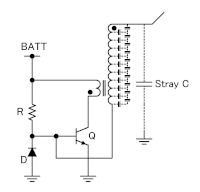
XXX . XXX 4% Spectrum Analyzer as like as microwave instrument
Spectrum analysis primarily measures power, frequency, and noise. It is concerned primarily with characterizing signal components (such as its spurious and harmonic components, modulation, noise, etc.) Spectrum analysis locates frequencies where microwave energy exists.
Distortion measurements
Distortion measurement is an area where the spectrum analyzer makes a significant contribution. There are two basic types of distortion that are usually specified by the manufacturer: harmonic distortion and two-tone, third-order intermodulation distortion. The third-order intermodulation products are represented by: 2f1 - f2 and 2f2 - f1, where f1 and f2 are the two-tone input signals.The HP 8565A can measure harmonic distortion products up to 100 dB down in the 1.7 to 22 GHz frequency range. Third-order intermodulation products can also be measured up to 100 dB down, depending on signal separation and frequency range. In all, the HP 8565A is capable of making a wide variety of distortion measurements with speed and precision.
Distortion in amplifiers
All amplifiers generate some distortion at the output and these distortion products can be significant if the amplifier is overdriven with a high-level input signal. The test setup in Figure 1 was used to measure the third-order intermodulation products of a microwave FET (field-effect transistor) amplifier. Directional couplers and attenuators were used to provide isolation between sources.Figure 2 is a CRT photo of a two-tone, third-order intermodulation measurement. The third-order products P(2f1 - f2) and P(2f2 - f1) are 50 dB below the two-tone signals P(f1) and P(f2). The difference between the power levels of the two-tone signals and the intermodulation products is known as the "intermodulation ratio". Note that if you adjust the power levels of the two tones P(f1) and P(f2) to be exactly equal in power, the power levels of the intermodulation products will be exactly equal as well. So tweak the power levels of P(f1) and P(f2) carefully or you will have several choices on the display to calculate the intermodulation ratio from.
Third-order intercept point measurement
If you measured and plotted the power levels P(f1) and P(2f2-f1) versus input power, eventually at some power level they would be equal. (We promise to get into this more in-depth in a future chapter on receivers. Unknown Editor) This is known as the "third-order intercept point", sometimes abbreviated TOI, sometimes IP3 or even other weird ways. The higher the TOI, the more power an amplifier can handle.The beautiful thing about the scope output in Figure 2 is that from this one picture the amplifier's TOI can be calculated. How is this possible without taking multiple sets of data and plotting the relationship between P(f1) and P(2f2-f1)? A phenomenon you need to be aware of is that the third-order modulation products increase 3 dB for every 1 dB that the input power of the two tones are increased, while the two-tone power levels only increase 1 dB/dB (thanks for the correction, Barrett!) Why does this happen? Let some scientist worry about that, just be glad that it does and use it to calculate the TOI from the data in Figure 2:
P(f1) = 0 dBmHow close should the two frequencies be for measuring intermodulation ratio and TOI? Why argue with an HP manual? Use 100 MHz separation, with 1 MHz resolution bandwidth.
P(2f2-f1) = -50 dBm
Intermodulation Ratio = P(f1) - P(2f2-f1) = 0 dB - (-50 dB) = 50 dB
TOI = P(f1) +1/2(Intermodulation Ratio) = 0 dBm + 25 dB = 25 dBm
One word of caution about TOI measurements: the actual intercept point is only a mathematical construct; you should never try to measure it directly. Chances are the DUT will blow up well before the four output tones are all equal in power!

Figure 1. Two-tone test setup

RES BW 1 MHz, REF LEVEL 0 dBm, LOG SCALE 10 db/
FREQUENCY 5.950 GHz, FREQ SPAN/DIV 50 MHz
Figure 2. Two-tone, third-order intermodulation products
Distortion in mixers
Mixers utilize the non-linear characteristics of an active or passive device to achieve a desired frequency conversion. This results in some distortion at the output due to the inherent non-linearity of the device. Figure 3 illustrates the test setup and CRT photograph of a typical mixer measurement.
Figure 3. Mixer measurement
Conversion loss (SSB):
RFin - IF = (-30) - (-40)= 10 dB
LO to IF Isolation:
LOin - LOout(IF) = (+5) - (-25)=30 dB
RF to IF Isolation:
RFin - RFout(IF) = (-30) - (-57)=27 dB
Third-Order Distortion Product (2 LO - RF)= -64 dBm @ 600 MHz.
Distortion in oscillators
Distortion in oscillators may be harmonically or non-harmonically related to the fundamental frequency. Non-harmonic oscillator outputs are usually termed spurious. Both harmonic and spurious outputs of an oscillator can be minimized with proper biasing and filtering techniques. The HP 8565A can monitor changes in distortion levels while modifications to the oscillator are made. In the full-hand modes, a tuning marker can be located under any signal response to determine its frequency and hence its relationship to the oscillator's fundamental frequency. Figure 4 is a CRT photo of the fundamental and second harmonic of an S-band (2-4 GHz) YIG oscillator. The internal preselector of the HP 8565A enables the analyzer to measure a low-level harmonic in the presence of a high level fundamental. The photo was obtained by adjusting the PERSIST control to allow storage of the trace and then tuning the oscillator over a narrow band.
RES BW 3 MHz, REF LEVEL 0 dBm, LOG SCALE 10 dB/
FREQUENCY 3.864 GHz, FREQ SPAN/DIV F Hz
FREQUENCY 3.864 GHz, FREQ SPAN/DIV F Hz
Figure 4. Oscillator fundamental and second harmonic
Modulation measurements
Amplitude modulation (AM) measurement
The wide dynamic range of the spectrum analyzer allows accurate measurement of modulation levels. A 0.06% modulation is a logarithmic ratio of 70 dB, which is easily measured with the HP 8565A. Figure 5 is a signal with 2% AM; a log ratio of 40 dB.
RES BW 3 kHz, REF LEVEL -20 dBm, LOG SCALE 10 dB/
FREQUENCY 1.067 GHz, FREQ SPAN/DIV 50 kHz
FREQUENCY 1.067 GHz, FREQ SPAN/DIV 50 kHz
Figure 5. 2% Amplitude Modulation
When the analyzer is used as a manually-tuned receiver (ZERO SPAN), the AM is demodulated and viewed in the time domain. To demodulate an AM signal, uncouple the RESOLUTION BW and set it to a value at least twice the modulation frequency. Then set the AMPLITUDE SCALE to LIN and center the signal, horizontally and vertically, on the CRT (see Figure 6). By pushing ZERO SPAN and VIDEO triggering, the modulation will be displayed in the time domain (see Figure 7.) The time variation of the modulation signal can then be measured with the calibrated SWEEP TIME/DIV control.
RES BW 1 MHz, REF LEVEL -18 dBm, LOG SCALE 10 dB/
FREQUENCY 1.067 GHz, FREQ SPAN/DIV 50 kHz
Figure 6. Linear Amplitude Display

RES BW 1 MHz, REF LEVEL -18 dBm, LOG SCALE 10 dB/
FREQUENCY 0.550 GHz, FREQ SPAN/DIV 0 kHz
FREQUENCY 0.550 GHz, FREQ SPAN/DIV 0 kHz
Figure 7. Demodulated AM signal in ZERO SPAN
Frequency modulation (FM) measurement
For frequency modulated signals, parameters such as modulation frequency (fm), modulation index (m), peak frequency deviation of carrier (Df peak) are all easily measured with the HP 8565A. The FM signal in Figure 8 was adjusted for the carrier null which corresponds to m = 2.4 on the Bessel function. The modulation frequency, fm, is simply the frequency separation of the sidebands which is 50 kHz. From this, we can calculate the peak frequency deviation of the carrier (Df peak) with the following equation:
RES BW 3 kHz, REF LEVEL -22dBm, LOG SCALE 10 dB/
FREQUENCY 0.098 GHz, FREQ SPAN/DIV 100 kHz
FREQUENCY 0.098 GHz, FREQ SPAN/DIV 100 kHz
Figure 8. FM signal
m=Although the HP 8565A does not have a built-in discriminator, FM signals can be demodulated by slope detection. Rather than tuning the signal to the center of the CRT as in AM, the slope of the IF filter is tuned to the center of the CRT instead. At the slope of the IF filter, the frequency variation is converted to amplitude variation. When ZERO SPAN is selected, the amplitude variation is detected by the analyzer and displayed in the time domain as shown in Figure 9. In FM, the RESOLUTION BW must be increased to yield a display similar to Figure 10 before switching to ZERO SPAN.f peak/fm or

RES BW 300 kHz, REF LEVEL -23 dBm,
FREQUENCY 0.098 GHz, FREQ SPAN/DIV 0 kHz
FREQUENCY 0.098 GHz, FREQ SPAN/DIV 0 kHz
Figure 9. Demodulated FM signal in ZERO SPAN

RES BW 300 kHz, REF LEVEL -23 dBm,
FREQUENCY 0.098 GHz, FREQ SPAN/DIV 200 kHz
FREQUENCY 0.098 GHz, FREQ SPAN/DIV 200 kHz
Figure 10. Slope detection of FM signal
Pulsed RF measurements
A pulsed RF signal is a train of RF pulses having constant amplitude. If you haven't encountered a pulsed RF signal in the lab, you ain't done squat! Some pulsed RF signal parameters parameters that can be determined directly on a spectrum analyzer include PRF (pulse repetition frequency), PRI (pulse repetition interval, which is the reciprocal of PRF), pulse width, duty cycle, peak and average pulsed power, and the on/off ratio of the modulator. Figure 11 illustrates a line spectrum presentation of a pulsed RF signal.
RES BW 10 kHz, REF LEVEL -20 dBm, LOG SCALE 10 dB/
FREQUENCY 2.402 GHz, FREQ SPAN/DIV 500 kHz
FREQUENCY 2.402 GHz, FREQ SPAN/DIV 500 kHz
Figure 11. Line spectrum of pulsed RF signal
A line spectrum (as opposed to a pulsed spectrum) is an actual Fourier representation of a pulsed RF signal in the frequency domain; all the spectral components of the signal are fully resolved. To obtain a line spectrum on the analyzer, the "rule of thumb" to follow is that the RESOLUTION BW be less than 0.3 x PRF. This ensures that individual spectral lines will be resolved. From the line spectrum shown in Figure 11, it is possible to measure the following parameters:
PRF = 50 kHz (the spacing between the spectral lines)Then from the above measurement the following data can be calculated:
PRI = 1/PRF = 20 microseconds
lobe width = 1MHz
mainlobe power = -48 dBm
Pulse width 1/(lobe width) = 1/1MHz=1A factor to consider when measuring the amplitude of a pulsed RF signal is the pulse desensitization factor. The mainlobe power of a pulsed RF signal does not represent the actual peak power of the signal. This is because a pulsed signal has its power distributed over a number of spectral components and each component represents a fraction of the peak pulse power. The spectrum analyzer measures the absolute power of each spectral component. To determine the peak pulse power in a line spectrum, a pulse desensitization factor (s
Duty Cycle=PRF/(lobe width) = 50kHz/(1MHz) = 0.05
For a duty cycle of 0.05,L = 20 log (duty cycle)
An alternate method of measuring a pulsed RF signal is in the pulse spectrum mode. In a pulse spectrum, the individual spectral lines are not resolved. If the RESOLUTION BW of the analyzer is greater than 1.7 x PRF, then the pulsed RF signal is being viewed in the pulse spectrum. Using the pulse spectrum enables a wider resolution bandwidth to be used. Two benefits result from this: first, the signal-noise ratio is increased because the pulse amplitude increases linearly with the resolution bandwidth (RBW) whereas random noise increases only proportionally to the square-root of the video bandwidth (VBW)1/2. Hence the signal-noise ratio of the analyzer is effectively increased. Secondly, faster sweep times can be used because of the wider resolution bandwidths. The HP 8565A has a 3 MHz RESOLUTION BW which enables it to effectively display pulsed RF signals in the pulse spectrum. The 3 MHz bandwidth, along with fast sweep times, also enables narrow pulse widths to be measured in the time domain. Figure 12 illustrates a signal in the pulse spectrum. The same signal is demodulated with the analyzer in Figure 13.

RES BW 30 kHz, REF LEVEL -1 dBm, LOG SCALE 10 dB/
FREQUENCY 2.402 GHz, FREQ SPAN/DIV 100 kHz
FREQUENCY 2.402 GHz, FREQ SPAN/DIV 100 kHz
Figure 12. Pulse spectrum

RES BW 3 MHz, REF LEVEL 0 dBm, LOG SCALE 10 dB/
FREQUENCY 2.402 GHz, FREQ SPAN/DIV 0 MHz
FREQUENCY 2.402 GHz, FREQ SPAN/DIV 0 MHz
Figure 13. Demodulated pulsed RF signal in ZERO SPAN
An additional factor to consider when measuring pulsed RF signals is the VIDEO FILTER control. In general, the VIDEO FILTER should be left in the OFF position when measuring pulsed RF signals. Adding video filtering will desensitize a pulsed signal and limit its displayed amplitude. Hence, when monitoring pulsed signals in a fullband mode, it is important to use the F mode rather than the FULL BAND pushbutton mode. The FULL BAND mode automatically engages a 9 kHz VIDEO FILTER (0.003 x 3 MHz) which will limit the displayed amplitude of the pulse.
Noise measurements
Applications involving noise measurements include oscillator noise (spectral purity), signal-noise ratio, and noise figure. The NOISE AVG position of the VIDEO FILTER control can be used to measure the analyzer sensitivity or noise power from 0.01 to 22 GHz.Noise figure measurement
(Note: the spectrum analyzer should only be used for noise figure measurements by poor bastards that don't have a noise figure meter available. Unknown Editor.) The test setup in Figure 14 is used to make a swept noise figure measurement of an amplifier. In general, this measurement involves determining the total gain of the amplifier under test and the pre-amp. Then the input of the amplifier is terminated and its noise power is measured. The noise figure of the amplifier will then be the theoretical noise power (KTB) minus the total gain and the amplifier noise power. Figure 15 is a photo of an amplifier's noise power output from 0.012 to 1.3 GHz.
Figure 14. Swept noise figure test setup

RES BW 3 MHz, REF LEVEL -30 dBm, LOG SCALE 10 dB/
FREQUENCY 1.300 GHz, FREQ SPAN/DIV F Hz
FREQUENCY 1.300 GHz, FREQ SPAN/DIV F Hz
Figure 15. Noise power measurement
Electromagnetic interference (EMI) measurement
The overall objective of EMI measurement is to assure compatibility between devices operating in the same vicinity. The HP 8565A, along with an appropriate transducer, is capable of measuring either conducted or radiated EMI. Figure 16 illustrates a simple setup used for measuring radiated field strength.
Figure 16. Field strength test setup
The antenna is used to convert the radiated field to a voltage for the analyzer to measure. The field strength will be the analyzer reading plus the antenna correction factor. Figure 17 illustrates a typical signal generated by a DUT (Device Under Test) with spurious radiation.

RES BW 300 kHz, REF LEVEL -10 dBm, LOG SCALE 10 dB/
FREQUENCY 0.226 GHz, FREQ SPAN/DIV 10 MHz
FREQUENCY 0.226 GHz, FREQ SPAN/DIV 10 MHz
Figure 17. Spurious radiation
Compatibility is also important for high-frequency circuits which are in close proximity to each other. In a multistage circuit, parasitic oscillation from one stage can couple to it nearby stage and cause unpredictable behavior. A popular technique used to search for spurious radiation is with an inductive loop probe. The loop probe is simply a few turns of wire that attaches to the spectrum analyzer with a flexible coaxial cable. (See Figure 18.)
Figure 18. Loop probe
Various parts of the circuit can then be "probed" to identify the location as well as the frequency and relative amplitude of a spurious signal. Once the spurious signal has been identified, design techniques can be implemented to reduce or eliminate the cause of interferenceexample of AR RF/Microwave Instrumentation
 The growth of the wireless market at higher frequency bands means that approximately half of all radio links manufactured are above 30 GHz. The 38 GHz band is significant with increasing interest in bands above 40 GHz, particularly 42 and 43 GHz. In this region, both point-to-point and point-to-multipoint radios for broadband wireless access are becoming available.
To manufacture and maintain such links demands test equipment with capability in this part of the spectrum. Fulfilling the requirement is the model 6845 10 MHz to 46 GHz Microwave Spectrum Analyzer with a full bandwidth, independently-controlled tracking generator.
Integrated into this single instrument are a synthesized source, a three-channel scalar analyzer and a spectrum analyzer. The inclusion of a 46 GHz tracking generator is of particular merit for engineers because it allows the 6845 to act as both transmitter and receiver when testing up and down links.
For insertion and reflection measurements, the tuned input of the 6845's spectrum analyzer gives a dynamic range of 70 dB at 40 GHz. The instrument is especially effective for frequency conversion measurements when the ability to set the spectrum analyzer and source frequencies independently in both CW and swept modes greatly simplifies the testing of mixers, up and down converters, and frequency multipliers and dividers. Figure 1 shows the instrument's display of a 38 GHz radio signal spectrum. Figure 2 shows the response of a 24 GHz high pass filter.
 | 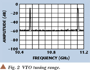 |
As an addition to the 6840 series, the 6845 incorporates the main features of the existing range. For instance, the integration of a source, spectrum analyzer and scalar analyzer into a single instrument means the operator uses a single interface to set up any measurements. This saves time and is easier than writing software to perform complex measurement tasks, such as frequency offset network measurements.
Eight soft keys give rapid access to all commonly used parameters and are shaped to inform the user of the action that the key will perform, such as enter data, select from list, move to another menu or immediate action. All commonly accessed functions are no more than one level deep.
To simplify operation a built-in applications interface allows the users to create their own measurement routines and guides the operator through the test procedure. For example, it can display on screen how to set up the measurement, lead the operator through a calibration, show where to connect the device under test and then test the device's performance against predefined limits.
A large thin-film technology (TFT) display shows up to four measurements on two channels, and scalar and spectrum measurements can be displayed simultaneously on independent channels. Alternatively, two spectrum channels can be shown with a wide and narrow frequency sweep. This could be used to scan a frequency spectrum for interfering signals, while simultaneously displaying the wanted carrier.
Up to eight markers are available. In spectrum mode the markers identify the frequency and level of a signal, position signals on the display and measure relative signal values. A peak search feature places markers on the eight highest signals displayed for spurious signal identification. A table displayed below the traces shows the values of all eight markers dynamically.
In scalar mode, markers automatically calculate peak-to-peak ripple, N - dB bandwidth, 1 dB compression point, and find the maximum and minimum signal levels. For fault location measurements the next peak left/right feature identifies the position and magnitude of each of the discontinuities along the transmission lines, with the peak find soft key used to quickly locate the biggest discontinuity on the line.
The 6845 provides real-time transmission line fault location with 0.1 percent accuracy, and its applications interface allows guided and automatic testing. The use of electrically erasable programmable read-only memory (EEPROM) corrected scalar detectors ensures accurate measurements, which can either be saved to internal non-volatile memory or to a 3.5" disk. Traces saved onto disk can then be either archived or imported into a spreadsheet for viewing.
By providing an integrated solution to component and subsystem testing from 10 MHz to 46 GHz the 6845 has particular relevance to the manufacturing, installation and maintenance of point-to-point and point-to-multipoint radios and satellite communications equipment. It is especially designed for testing components and assemblies used in radio and military systems.
For component and subsystem design engineers, the flexibility provided by the instrument's integrated testing solution can help reduce design time. For installation and maintenance engineers it provides a quick and convenient method of measuring return loss and fault location on antennas and feeders at mobile communications basestations, as well as verifying radio performance through the modulation spectrum.
Other applications include measuring for compliance with specifications on emissions, which must be below a specified level and can run up to 44 GHz. Similarly, test houses have a requirement to measure components at these frequencies, particularly for electromagnetic compatibility and Conformite European (CE) marking activities.
Also, for those out in the field maintaining radio links at frequencies above 30 GHz, the fact that the spectrum analyzer is incorporated into the same box as an instrument that enables the measurement of SWRs is a benefit.
Whether in the laboratory, on the factory floor or out in the field, an instrument's reliability and capability for future expansion are paramount. That is why the 6845 Microwave System Analyzer is of modular design for rapid servicing and includes expansion slots for ease of upgrading to accommodate additional modules and options
Modern microwave concept :
method for spectral analysis of microwave signals that employs time-domain processing in fiber. We use anomalous dispersion in single-mode fiber to perform a Fresnel transform followed by a matched amount of dispersion-compensating fiber to perform an inverse Fresnel transform of an ultrashort pulse. After the Fresnel-transformed waveform is modulated by the microwave signal, the waveform at the output of the dispersion-compensating fiber represents the ultrashort pulse convolved with the microwave spectrum. An experimental system for spectral analysis of microwave signals in the range 6–21 GHz .
Monolithic microwave integrated circuit

.svg)
MMICs are dimensionally small (from around 1 mm² to 10 mm²) and can be mass-produced, which has allowed the proliferation of high-frequency devices such as cellular phones. MMICs were originally fabricated using gallium arsenide (GaAs), a III-V compound semiconductor. It has two fundamental advantages over silicon (Si), the traditional material for IC realisation: device (transistor) speed and a semi-insulating substrate. Both factors help with the design of high-frequency circuit functions. However, the speed of Si-based technologies has gradually increased as transistor feature sizes have reduced, and MMICs can now also be fabricated in Si technology. The primary advantage of Si technology is its lower fabrication cost compared with GaAs. Silicon wafer diameters are larger (typically 8" or 12" compared with 4" or 6" for GaAs) and the wafer costs are lower, contributing to a less expensive IC.
Originally, MMICs used MEtal-Semiconductor Field-Effect Transistors (MESFETs) as the active device. More recently High Electron Mobility Transistors (HEMTs), Pseudomorphic HEMTs and Heterojunction Bipolar Transistors have become common.
Other III-V technologies, such as indium phosphide (InP), have been shown to offer superior performance to GaAs in terms of gain, higher cutoff frequency, and low noise. However they also tend to be more expensive due to smaller wafer sizes and increased material fragility.
Silicon germanium (SiGe) is a Si-based compound semiconductor technology offering higher-speed transistors than conventional Si devices but with similar cost advantages.
Gallium nitride (GaN) is also an option for MMICs. Because GaN transistors can operate at much higher temperatures and work at much higher voltages than GaAs transistors, they make ideal power amplifiers at microwave frequencies.
XXX . XXX 4%zero null 0 what is Spectrum Analyzer ?
RF spectrum analyzers are an essential tool for RF and other engineers, providing a view of the spectrum of signals with their amplitudes and frequencies.
Spectrum analyzers are widely used within the electronics industry for analysing the frequency spectrum of radio frequency, RF and audio signals. Looking at the spectrum of a signal they are able to reveal elements of the signal, and the performance of the circuit producing them that would not be possible using other means.
Spectrum analysers are able to make a large variety of measurements and this means that they are an invaluable tool for the RF design development and test laboratories, as well as having many applications for specialist field service.

A typical bench spectrum analyser

A handheld spectrum analyzer
Why spectrum analysis?
The most natural way to look at waveforms is in the time domain - looking at how a signal varies in amplitude as time progresses, i.e. in the time domain. This is what an oscilloscope is used for, and it is quite natural to look at waveforms on an oscilloscope display. However this is not the only way in which signals can be displayed.A French mathematician and physicist, named Jean Baptiste Joseph Fourier, who lived from 1768 to 1830 also started to look at how signals are seen in another format, in the frequency domain where signals are viewed as a function of their frequency rather than time. He discovered that any waveform seen in the time domain, there is an equivalent representation in the frequency domain. Expressed differently, any signal is made up from a variety of components of different frequencies. One common example is a square waveform. This is made up from signal comprising the fundamental as well as third, fifth, seventh, ... harmonics in the correct proportions.
In exact terms it is necessary that the signal must be evaluated over an infinite time for the transformation to hold exactly. However in reality it is sufficient to know that the waveform is continuous over a period of at least a few seconds, or understand the effects of changing the signal.
It is also worth noting that the mathematical Fourier transformation also accommodates the phase of the signal. However for many testing applications the phase information is not needed and considerably complicates the measurements and test equipment. Also the information is normally not needed, and only the amplitude is important.
By being able to look at signals in the time domain provides many advantages and in particular for RF applications, although audio spectrum analyzers are also widely used. Looking at signals in the frequency domain with a spectrum analyzer enables aspects such as the harmonic and spurious content of a signal to analyzed. Also the width of signals when modulation has been applied is important. These aspects are of particular importance for developing RF signal sources, and especially any form of transmitter including those in cellular, Wi-Fi, and other radio or wireless applications. The radiation of unwanted signals will cause interference to other users of the radio spectrum, and it is therefore very important to ensure any unwanted signals are kept below an acceptable level, and this can be monitored with a spectrum analyzer.
Spectrum analyzer basics
There are many different types of RF test equipment that can be used for measuring a variety of different aspects of an RF signal. It is therefore essential to choose the right type of RF test equipment to meet the measurement requirements for the particular job in hand.| Test Instrument Type | Frequency measurement | Intensity / amplitude measurement | Application |
|---|---|---|---|
| Power meter | N | Y | Use for accurate total power measurements |
| Frequency counter | Y | N | Used to provide very accurate measurements of the dominant frequency within a signal |
| Spectrum analyser | Y | Y | Used primarily to display the spectrum of a radio frequency signal. Can also be used to make power and frequency measurements, although not as accurately as dedicated instruments |
| RF network analyser | Y | Y | Used to measure the properties of RF devices |
The spectrum analyzer is able to offer a different measurement capability to other instruments. Its key factor is that it is able to look at signals in the frequency domain, i.e. showing the spectrum, it is possible to see many new aspects of the signal.
An analyser display, like that of an oscilloscope has two axes. For the spectrum analyser the vertical axis displays level or amplitude, whereas the horizontal axis displays frequency. Therefore as the scan moves along the horizontal axis, the display shows the level of any signals at that particular frequency.
This means that the spectrum analyser, as the name indicates analyses the spectrum of a signal. It shows the relative levels of signals on different frequencies within the range of the particular sweep or scan.

General format of the display on a spectrum analyzer
In view of the very large variations in signal level that are experienced, the vertical or amplitude axis is normally on a logarithmic scale and is calibrated in dB in line with many other measurements that are made for signal amplitudes. The horizontal scale conversely is normally linear. This can be adjusted to cover the required range. The term span is used to give the complete calibrated range across the screen. Terms like scan width per division may also be used and refer to the coverage between the two major divisions on the screen.
Summary of spectrum analyser types
There are a number of different categories for spectrum analyzers. Some of the main spectrum analyser types are noted below:- Swept or superheterodyne spectrum analysers: The operation of the swept frequency spectrum analyzer is based on the use of the superheterodyne principle, sweeping the frequency that is analysed across the required band to produce a view of the signals with their relative strengths. This may be considered as the more traditional form of spectrum analyser, and it is the type that is most widely used.
Read more about the Swept spectrum analyser - Fast Fourier Transform, FFT analysers: These spectrum analyzers use a form of Fourier transform known as a Fast Fourier Transform, FFT, converting the signals into a digital format for analysis digitally. These analysers are obviously more expensive and often more specialised. Read more about the FFT spectrum analyser
- Real-time analysers: These test instruments are a form of FFT analyser. One of the big issues with the initial FFT analyser types was that they took successive samples, but with time gaps between the samples. This gave rise to some issues with modulated signals or transients as not all the information would be captured. Requiring much larger buffers and more powerful processing, realtime spectrum analyser types are able to offer the top performance in signal analysis. Read more about the Real-time spectrum analyser
- Audio spectrum analyzer: Although not using any different basic technology, audio spectrum analyzers are often grouped differently to RF spectrum analyzers. Audio spectrum analyzers are focussed, as the name indicates, on audio frequencies, and this means that low frequency techniques can be adopted. This makes them much cheaper. It is even possible to run them on PCs with a relatively small amount of hardware - sometimes even a sound card may suffice for some less exacting applications.
Spectrum analyser advantages and disadvantages
Both swept / superheterodyne and FFT analyzer technologies have their own advantages. The more commonly used technology is the swept spectrum analyser as it the type used in a general-purpose test instruments and this technology is able to operate at frequencies up to many GHz. However it is only capable of detecting continuous signals, i.e. CW as time is required to capture a given sweep, and they are not able to capture any phase information.FFT analyzer analyser technology is able to capture a sample very quickly and then analyse it. As a result an FFT analyzer is able to capture short lived, or one-shot phenomena. They are also able to capture phase information. However the disadvantage of the FFT analyzer is that its frequency range is limited by the sampling rate of the analogue to digital converter, ADC. While ADC technology has improved considerably, this places a major limitation on the bandwidths available using these analyzers.
In view of the fact that both FFT and superheterodyne / swept instrument technologies have their own advantages, many modern analyzers utilise both technologies, the internal software within the unit determining the best combinations for making particular measurements. The superheterodyne circuitry enabling basic measurements and allowing the high frequency capabilities, whereas the FFT capabilities are introduced for narrower band measurements, and those where fast capture is needed.
An analyzer will often determine the best method dependent upon factors including the filter settling time and sweep speed. If the spectrum analyser determines it can show the spectrum faster by sampling the required bandwidth, processing the FFT and then displaying the result, it will opt for an FFT approach, otherwise it will use the more traditional fully superheterodyne / sweep approach. The difference between the two measurement techniques as seen by the user is that using a traditional sweep approach, the result will be seen as sweep progresses, when an FFT measurement is made, the result cannot be displayed until the FFT processing is complete.
the sweep spectrum analyser, or as it is also known the swept or superheterodyne test instrument a summary or tutorial about the sweep or superheterodyne format of spectrum analyser that sweeps the required span with block diagram and operational details.
Of the two types of RF spectrum analyzer that are available, namely the swept or superheterodyne spectrum analyzer and the Fast Fourier Transform, FFT spectrum analyzer, it is the swept or sweep spectrum analyzer that is the most widely used.
The swept spectrum analyser is the general workhorse RF test equipment of the spectrum analyzer family. It is a widely used item of RF test equipment that is capable of looking at signals in the frequency domain. In this way this form of spectrum analyser is able to reveal signals that are not visible when using other items of test equipment.
To enable the most effective use to be made of a sweep spectrum analyzer it is necessary to have a basic understanding of the way in which it works. This will enable many of the pitfalls, including false readings, using an analyzer to be avoided.
Advantages & disadvantages of a sweep spectrum analyzer
The sweep or swept spectrum analyzer has a number of advantages and disadvantages when compared to the main other type of analyzer known as the FFT spectrum analyzer. When choosing which type will be suitable, it is necessary to understand the differences between them and their relative merits.Advantages of superheterodyne spectrum analyser technology
- Able to operate over wide frequency range: Using the superheterodyne principle, this type of spectrum analyzer is able to operate up to very high frequencies - many extend their coverage to many GHz.
- Wide bandwidth: Again as a result of the superheterodyne principle this type of spectrum analyzer is able to have very wide scan spans. These may extend to several GHz in one scan.
- Not as expensive as other spectrum analyzer technologies: Although spectrum analyzers of all types are expensive, the FFT style ones are more expensive for a similar level of performance as a result of the high performance ADCs in the front end. This means that for the same level of base performance, the superheterodyne or sweep spectrum analyzer is less expensive.
- Cannot measure phase: The superheterodyne or sweep spectrum analyzer is a scalar instrument and unable to measure phase - it can only measure the amplitude of signals on given frequencies.
- Cannot measure transient events: FFT analyzer technology is able to sample over a short time and then process this to give the required display. In this way it is able to capture transient events. As the superheterodyne analyzer sweeps the bandwidth required, this takes longer and as a result it is unable to capture transient events effectively.
Sweep spectrum analyser basics
The swept spectrum analyser uses the same superheterodyne principle used in many radio receivers as the underlying principle on which its operation depends. The superheterodyne principle uses a mixer and a second locally generated local oscillator signal to translate the frequency.The mixing principle used in the analyzer operates in exactly the same manner as it does for a superheterodyne radio. The signal entering the front end is translated to another frequency, typically lower in frequency. Using a fixed frequency filter in the intermediate frequency section of the equipment enables high performance filters to be used, and the analyzer or receiver input frequency can be changed by altering the frequency of the local oscillator signal entering the mixer.
Although the basic concept of the spectrum analyzer is exactly the same as the superheterodyne radio, the particular implementation differs slightly to enable it to perform is function.

Superheterodyne or swept frequency spectrum analyzer block diagram
The frequency of the local oscillator governs the frequency of the signal that will pass through the intermediate frequency filter. This is swept in frequency so that it covers the required band. The sweep voltage used to control the frequency of the local oscillator also controls the sweep of the scan on the display. In this way the position of the scanned point on the screen relates to the position or frequency of the local oscillator and hence the frequency of the incoming signal. Also any signals passing through the filter are further amplified, detected and often compressed to create an output on a logarithmic scale and then passed to the display Y axis.
Elements of a sweep spectrum analyzer
Although the basic concept of the sweep spectrum analyser is fairly straightforward a few of the circuit blocks may need a little further explanation.- RF attenuator: The first element a signal reaches on entering the test instrument is an RF attenuator. Its purpose is to adjust the level of the signal entering the mixer to its optimum level. If the signal level is too high, not only may the reading fall outside the display, but also the mixer performance may not be optimum. It is possible that the mixer may run outside is specified operating region and additional mix products may be visible and false signals may be seen on the display.
In fact when false signals are suspected, the input attenuator can be adjusted to give additional attenuation, e.g. +10 dB. If the signal level falls by more than this amount then it is likely to be an unwanted mix product and insufficient RF attenuation was included for the input signal level.
The input RF attenuator also serves to provide some protection to very large signals. It is quite possible for very large signals to damage the mixer. As these mixers are very high performance components, they are not cheap to replace. A further element of protection is added. Often the input RF attenuator includes a capacitor and this protects the mixer from any DC that may be present on the line being measured. - Low pass filter and pre-selector: This circuit follows the attenuator and is included to remove out-of-band signals which it prevents from mixing with the local oscillator and generating unwanted responses at the IF. These would appear as signals on the display and as such must be removed.
Microwave spectrum analyzers often replace the low pass filter with a more comprehensive pre-selector. This allows through a band of frequencies, and its response is obviously tailored to the band of interest - Mixer: The mixer is naturally key to the success of the analyser. As such the mixers are high performance items and are generally very expensive. They must be able to operate over a very wide range of signals and offer very low levels of spurious responses. Any spurious signals that are generated may mix with incoming signals and result in spurious signals being seen on the display. Thus the dynamic range performance of the mixer is of crucial importance to the analyser as a whole.
Great care must be taken when using a sweep spectrum analyzer not to feed excessive power directly into the mixer otherwise damage can easily occur. This can happen when testing radio transmitters where power levels can be high and accidentally turning the attenuator to a low value setting so that higher power levels reach the mixer. As a result it is often good practice to use an external fixed attenuator that is capable of handling the power. If damage occurs to the mixer it will disable the spectrum analyzer and repairs can be costly in view of the high performance levels of the mixer. - IF amplifier: Despite the fact that attenuation is provided at the RF stage, there is also a necessity to be able to alter the gain at the intermediate frequency stages. This is often used and ensures that the IF stages provide the required level of gain. It has to be used in conjunction with the RF gain control. Too high a level of IF gain will increase the front end noise level which may result in low level signals being masked. Accordingly the RF gain control should generally be kept as high as possible without overloading the mixer. In this way the noise performance of the overall test instrument is optimised.
- IF filter: The IF filters restrict the bandwidth that is viewed, effectively increasing the frequency resolution. However this is at the cost of a slower scan rate. Narrowing the IF bandwidth reduces the noise floor and enables lower level spurious signals to be viewed.
- Local oscillator: The local oscillator within the spectrum analyzer is naturally a key element in the whole operation of the unit. Its performance governs many of the overall performance parameters of the whole analyser. It must be capable of being tuned over a very wide range of frequencies to enable the analyzer to scan over the required range. It must also have a very good phase noise performance. If the oscillator has a poor phase noise performance then it will not only result in the unit not being able to make narrow band measurements as the close in phase noise on the local oscillator will translate onto the measurements of the signal under test, but it will also prevent it making any meaningful measurements of phase noise itself - a measurement being made increasingly these days.
- Ramp generator: The ramp generator drives the sweep of the local oscillator and also the display. In this way the horizontal axis of the display is directly linked to the frequency. In other words the ramp generator is controlled by the sweep rate adjustment on the spectrum analyser.
- Envelope or level detector: The envelope detector converts the signal from the IF filter into a signal voltage that can be passed to the display. As the level detector has to accommodate very large signal differences, linearity and wide dynamic range are essential.
The type of detector may also have a bearing on the measurement made. Whether the detector is an average level detector or whether it provides an RMS value.
An RMS detector calculates the power for each pixel of the displayed trace from samples allocated to the pixel, i.e. for the bandwidth that the pixel represents. The voltage for each sample is squared, summed and the result divided by the number of samples. The square root is then taken to give the RMS value.
For an average value, the samples are summed, and the result is divided by the number of samples. - Display: In many respects the display is the heart of the test instrument as this is where the signal spectra are viewed. The overall display section of the spectrum analyser contains a significant amount of processing to enable the signals to be viewed in a fashion that is easy comprehend. Items such as markers for minimum signal, maximum peak, auto peak, highlighting and many more elements are controlled by the signal processing in this area. These features and many more come as the result of significant increases in the amount of processing provided.
As for the display screens themselves, cathode ray tubes were originally used, but the most common form of display nowadays are forms of liquid crystal displays. The use of liquid crystal displays does have some limitations, but overall with the level of development in this technology they enable the required flexibility to be provided.
The superheterodyne spectrum analyser, or as it is also called the sweep spectrum analyser is still widely used although with the development of processing technology, other forms of analyser such as the FFT spectrum analyser are becoming increasingly widely used. However the superheterodyne analyser is able to provide a particularly useful function within the analyser marketplace.
FFT Spectrum Analyzer
- the Fast Fourier Transform spectrum analyser uses digital signal processing techniques to provide in depth waveform analysis with greater flexibility than other methods.
The FFT or Fast Fourier Transform spectrum analyser uses digital signal processing techniques to analyser a waveform with Fourier transforms to provide in depth analysis of signal waveform spectra.With the FFT analyzer able to provide facilities that cannot be provided by swept frequency analyzers, enabling fast capture and forms of analysis that are not possible with sweep / superheterodyne techniques alone.
Advantages and disadvantages of FFT analyzer technology
As with any form of technology, FFT analysers have their advantages and disadvantages:Advantages of FFT spectrum analyzer technology
- Fast capture of waveform: In view of the fact that the waveform is analysed digitally, the waveform can be captured in a relatively short time, and then the subsequently analysed. This short capture time can have many advantages - it can allow for the capture of transients or short lived waveforms.
- Able to capture non-repetitive events: The short capture time means that the FFT analyzer can capture non-repetitive waveforms, giving them a capability not possible with other spectrum analyzers.
- Able to analyse signal phase: As part of the signal capture process, data is gained which can be processed to reveal the phase of signals.
- Waveforms can be stored Using FFT technology, it is possible to capture the waveform and analyse it later should this be required.
- Frequency limitations: The main limit of the frequency and bandwidth of FFT spectrum analyzers is the analogue to digital converter, ADC that is used to convert the analogue signal into a digital format. While technology is improving this component still places a major limitation on the upper frequency limits or the bandwidth if a down-conversion stage is used.
- Cost: The high level of performance required by the ADC means that this item is a very high cost item. In addition to all the other processing and display circuitry required, this results in the costs rising for these items.
Fast Fourier Transform
At the very heart of the concept of the FFT analyzer is the fast Fourier Transform itself. The fast Fourier Transform, FFT uses the same basic principles as the Fourier transform, developed by Joseph Fourier (1768 - 1830) in which one value in, say, the continuous time domain is converted into the continuous frequency domain, including both magnitude and phase information.However to capture a waveform digitally, this must be achieved using discrete values, both in terms of the values of samples taken, and the time intervals at which they are taken. As the time domain waveform is taken at time intervals, it is not possible for the data to be converted into the frequency domain using the standard Fourier transform. Instead a variant of the Fourier transform known as the Discrete Fourier Transform, DFT must be used.
As the DFT uses discrete samples for the time domain waveform, this reflects into the frequency domain and results in the frequency domain being split into discrete frequency components of "bins." The number of frequency bins over a frequency band is the frequency resolution. To achieve greater resolution, a greater number of bins is needed, and hence in the time domain a large number of samples is required. As can be imagined, this results in a much greater level of computation, and therefore methods of reducing the amount of computation required is needed to ensure that the results are displayed in a timely fashion, although with today's vastly increased level of processing power, this is less of a problem. To ease the processing required, a Fast Fourier Transform, FFT is used. This requires that the time domain waveform has a the number of samples equal to a number which is an integral power of two.
FFT spectrum analyzer
The block diagram and topology of an FFT analyzer are different to that of the more usual superheterodyne or sweep spectrum analyzer. In particular circuitry is required to enable the digital to analogue conversion to be made, and then for processing the signal as a Fast Fourier Transform.The FFT spectrum analyzer can be considered to comprise of a number of different blocks:

FFT Spectrum Analyser Block Diagram
- Analogue front end attenuators / gain: The test instrument requires attenuators of gain stages to ensure that the signal is at the right level for the analogue to digital conversion. If the signal level is too high, then clipping and distortion will occur, too low and the resolution of the ADC and noise become a problems. Matching the signal level to the ADC range ensures the optimum performance and maximises the resolution of the ADC.
- Analogue low pass anti-aliasing filter: The signal is passed through an anti-aliasing filter. This is required because the rate at which points are taken by the sampling system within the FFT analyzer is particularly important. The waveform must be sampled at a sufficiently high rate. According to the Nyquist theorem a signal must be sampled at a rate equal to twice that of the highest frequency, and also any component whose frequency is higher than the Nyquist rate will appear in the measurement as a lower frequency component - a factor known as "aliasing". This results from the where the actual values of the higher rate fall when the samples are taken. To avoid aliasing a low pass filter is placed ahead of the sampler to remove any unwanted high frequency elements. This filter must have a cut-off frequency which is less than half the sampling rate, although typically to provide some margin, the low pass filter cut-off frequency is at highest 2.5 times less than the sampling rate of the analyzer. In turn this determines the maximum frequency of operation of the overall FFT spectrum analyzer.
- Sampling and analogue to digital conversion: In order to perform the analogue to digital conversion, two elements are required. The first is a sampler which takes samples at discrete time intervals - the sampling rate. The importance of this rate has been discussed above. The samples are then passed to an analogue to digital converter which produces the digital format for the samples that is required for the FFT analysis.
- FFT analyzer: With the data from the sampler, which is in the time domain, this is then converted into the frequency domain by the FFT analyzer. This is then able to further process the data using digital signal processing techniques to analyze the data in the format required.
- Display: With the power of processing it is possible to present the information for display in a variety of ways. Today's displays are very flexible and enable the information to be presented in formats that are easy to comprehend and reveal a variety of facets of the signal. The display elements of the FFT spectrum analyzer are therefore very important so that the information captured and processed can be suitably presented for the user.
the Real Time Spectrum Analyzer with operational details and how they work.
In recent years a form of spectrum analyser, termed a real-time spectrum analyser, RSA has grown in popularity.
These real-time spectrum analyzers are particularly useful in looking at waveforms where changes may be seen, and need to be captured. Often spectrum analysers that take time to process the waveforms may miss spurious signals and these can be particularly important when testing for compliance and out-of-band signals.
As the name implies, real-time spectrum analyzers operate in real time.
Real time spectrum analyzer basics
A real time spectrum analyzer operates in a different way to that of a normal swept or super heterodyne spectrum analyzer.The analyzer can acquire a particular bandwidth or span either side of a centre frequency. The analyzer captures all the signals within the bandwidth and analyses them in real time.
To achieve their performance a real time spectrum analyzer captures the waveform in memory and then uses a fast Fourier transform technology to analyzer the waveform very quickly, i.e. in real-time.
By analyzing the waveform in this way, transient effects that may not be visible on other forms of spectrum analyzer can be captured and highlighted.
There are a number of characteristics of real time spectrum analyzers:
- They are based around an FFT - Fast Fourier Transform spectrum analyzer. This will have a real-time - very fast - digital signal processing engine capable to processing the entire bandwidth with no gaps.
- An ADC - analogue to digital converter capable of digitizing he entire bandwidth of the pass band.
- Sufficient capture memory to enable continuous acquisition over the desired measurement period.
These real-time spectrum analyzers are particularly useful in looking at waveforms where changes may be seen, and need to be captured. Often spectrum analysers that take time to process the waveforms may miss spurious signals and these can be particularly important when testing for compliance and out-of-band signals.
As the name implies, real-time spectrum analysers operate in real time.
Realtime spectrum analyser basics
A realtime spectrum analyser operates in a different way to that of a normal swept or superheterodyne spectrum analyser.The analyser can acquire a particular bandwidth or span either side of a centre frequency. The analyser captures all the signals within the bandwidth and analyses them in real time.
To achieve their performance a real time spectrum analyser captures the waveform in memory and then uses a fast Fourier transform technology to analyse the waveform very quickly, i.e. in real-time.
By analysing the waveform in this way, transient effects that may not be visible on other forms of spectrum analyser can be captured and highlighted.
There are a number of characteristics of realtime spectrum analyzers:
- They are based around an FFT - Fast Fourier Transform spectrum analyser. This will have a real-time - very fast - digital signal processing engine capable to processing the entire bandwidth with no gaps.
- An ADC - analogue to digital converter capable of digitising he entire bandwidth of the passband.
- Sufficient capture memory to enable continuous acquisition over the desired measurement period
Spectrum analyser specifications are used to determine whether a particular test instrument will be able to meet the requirements placed upon it.
There are several different specifications, each detailing different aspects of the performance of the instrument.
When choosing a spectrum analyser, it is necessary to use the data sheet detailing all of the specifications to determine whether the instrument will be able provide the required results.
Frequency coverage
The frequency coverage of the spectrum analyser is one of the basic specifications or parameters. When determining whether a particular spectrum analyzer is suitable for the application, it is necessary to consider the maximum frequencies that will need to be viewed. It is worth remembering that the maximum frequency to be viewed should include the harmonics and intermodulation products of the wanted signals.Normally the frequency range must be such that harmonics of the fundamental and other important spurious signals can be viewed. To achieve this the analyser frequency range must extend well beyond the fundamental frequency of the signal. Often the figure used is ten times that of the fundamental, although often it is necessary to settle for top frequencies of less than this, especially for RF applications where the very high frequencies required may place a significant cost penalty on achieving this specification.
The lowest frequency specification may also be important. As spectrum analysers are often AC coupled, there will be a lower cut-off point. This should be checked.
Amplitude accuracy
The amplitude accuracy is a major spectrum analyzer specification. While the accuracy of a spectrum analyzer itself will not match that of a dedicated power meter for example, the accuracy of the individual level measurements need to be accurate to enable useful measurements to be made.The amplitude accuracy specification of a spectrum analyzer is determined by a number of factors, including the basic accuracy of the instrument as well as its frequency response. This means that the frequency elements should also be taken into consideration. Often accuracy levels of the order of ± 0.4 dB are achievable.
For microwave spectrum analyzers a YIG oscillator is normally used. As YIGs are highly non-linear devices, and as a result the amplitude accuracy specification figures will be less (typically ± 1 dB) when the YIG oscillator is used.
Some spectrum analyzers incorporate a power meter which operates with the analyzer to provide a very accurate measurement specification. For this, the spectrum analyser has a special power sensor that calibrates the input level at a number of absolute level points, then uses the very good linearity of the analyser to very accurately measure levels over the full range which may be in excess of 100dB.
Frequency accuracy specification
Most spectrum analyzers today employ frequency synthesized sources. This means that the accuracy of the frequency measurement is governed by that of the peak detection circuitry, detecting where the centre of a signal is, and also the accuracy of the reference source within the frequency synthesizer.Spectrum analyzers can be used as extremely accurate frequency counters with relatively high specifications. They locate a signal and track it, simultaneously with measuring it's absolute frequency. This can be particularly advantageous in many applications.
Spectrum analyzer sensitivity specification
In order to determine the low signal performance of spectrum analyzer a sensitivity specification is normally given. This is normally specified in terms of dBm / Hz at a given frequency.If a noise figure specification is required, then this can be calculated:
If a further improvement in the sensitivity or noise figure specification is required, then it is possible to add a low noise pre-amplifier.
Phase noise specification
There are many instances when the phase noise of a signal source, e.g. a transmitter, receiver local oscillator, etc needs to be measured. When this is the case, the phase noise specification of the spectrum analyzer is of particular importance. It should be better than the signal source being measured, typically by at least 10 dB for it not to affect the readings being made. For these applications, the spectrum analyser specification for phase noise needs to be carefully considered.Techniques apart from a straight measurement can be sued to improve the operation of the spectrum analyzer. These techniques include a noise correction process, where the noise of the spectrum analyzer is subtracted from the measurement. For higher performance it is possible to utilise cross-correlated phase noise measurements where the spectrum analyzer is effectively able to remove the phase noise of its internal local oscillators from the measurement. This process allows phase noise measurements to be made below the physical thermal limit, i.e. better than -174dBm/Hz.
Spectrum analyzer dynamic range
Dynamic range is a particularly important parameter for any spectrum analyzer. This type of test equipment is normally used on a logarithmic scale and is required to look at signals with enormously wide level ranges. Therefore the ability of the spectrum analyzer to accurately look at small signals in the presence of relatively close strong signals is particularly important.Spectrum analyzer tracking generator
- tracking generators can be used with many spectrum analyzers to enable them to be used as a scalar RF network analyzer.
A tracking generator provides spectrum analyzers with additional measurement capability beyond that of the basic spectrum analyser.The tracking generator enables some basic network measurements to be made, therby providing additional capability beyond basic spectrum analysis.
In view of this a tracking generator considerably extends the applications for which a spectrum analyzer can be used, making them more flexible and versatile.
Tracking generator basics
Normally spectrum analyzers are what may be termed passive instruments, making measurements of signals applied to them. Typically they may be used for measuring the spectra of oscillators, transmitters or other signals in RF systems. They measure signals in the frequency domain rather than the time, and this makes them ideal for looking at many RF signals.In their basic form, analyzers are not able to make response or network measurements. These types of measurements require signals to be applied to a particular device or network under test, and then measuring the response or output.
In order to make a network measurement like this, it is necessary to have a source to stimulate the device under test, and then a receiver is needed to measure the response. In this way it is possible to make a variety of network measurements including frequency response, conversion loss, return loss, and other measurements such as gain versus frequency, etc..
There are two items of test equipment that can be made to make these stimulus-response measurements. Possibly the most obvious type of test equipment is an RF network analyzer and the other is a spectrum analyzer with a tracking generator. If phase information is required, then it is necessary to use a vector network analyzer, but it possible to use a spectrum analyzer tracking generator arrangement for many other measurements. As many laboratories will already use a spectrum analyzer, the tracking generator approach is particularly attractive. In addition to this, tracking generators are incorporated into many spectrum analyzers as standard. This means that it is possible to use these test instruments to make many network measurements at no additional cost.
What is a tracking generator?
A spectrum analyzer tracking generator operates by providing a sinusoidal output to the input of the spectrum analyzer. The by linking the sweep of the tracking generator to the spectrum analyzer, the output of the tracking generator is on the same frequency as the spectrum analyzer, and the two units track the same frequency.Spectrum Analyser and Tracking Generator Diagram
If the output of the tracking generator was connected directly to the input of the spectrum analyzer, a single flat line would be seen with the level reflecting the output level of the tracking generator.
If a device under test, such as a filter is placed between the output of the tracking generator and the input of the spectrum analyzer, then the response of the device under test will alter the level of the tracking generator signal seen by the spectrum analyzer, and the level indicated on the analyzer screen. In this way the response of the device under test will be seen on the analyzer screen.
Using a tracking generator
Using tracking generators is normally very easy. As a tracking generator is either built into the spectrum analyzer, or is manufactured as an external option for a test instrument, then there are few issues with their use. However there are a few standard precautions to remember when using one:- Adjust tracking generator to centre of analyse passband: There is often an adjustment for the tracking oscillator to trim its frequency. Before using the tracking generator, it is wise to adjust the frequency trim adjustment to ensure that it is on exactly the same frequency as the spectrum analyzer. This is achieved by maximising the reading on the spectrum analyzer display.
- Calibrate system using direct connection: To ensure that any cable losses are known, it is always wise to replace the device under test with a back-to-back connector, or other short connecting line. In this way, the system will reveal any losses which it may be possible to "calibrate out".
using a spectrum analyzer: how to use it to make radio frequency tests and measurements.
Spectrum analyzers are an invaluable item of electronic test equipment used in the design, test and maintenance of radio frequency circuitry and equipment.
Spectrum analysers, like oscilloscopes are a basic tool used for observing signals. However, where oscilloscopes look at signals in the time domain, spectrum analyzers look at signals in the frequency domain. Thus a spectrum analyser will display the amplitude of signals on the vertical scale, and the frequency of the signals on the horizontal scale.
In view of the way in which a spectrum analyzer displays its output, it is widely used for looking at the spectrum being generated by a source. In this way the levels of spurious signals including harmonics, intermodulation products, noise and other signals can be monitored to discover whether they conform to their required levels.
Additionally using spectrum analysers it is possible to make measurements of the bandwidth of modulated signals can be checked to discover whether they fall within the required mask. Another way of using a spectrum analyzer is in checking and testing the response of filters and networks. By using a tracking generator - a signal generator that tracks the instantaneous frequency being monitored by the spectrum analyser, it is possible to see the loss at any given frequency. In this way the spectrum analyser makes a plot of the frequency response of the network.
Spectrum analyser display
A key element of using a spectrum analyser is in understand in the display.The purpose of a spectrum analyzer is to provide a plot or trace of signal amplitude against frequency. The display has a graticule which typically has ten major horizontal and ten major vertical divisions.

The horizontal axis of the analyzer is linearly calibrated in frequency with the higher frequency being at the right hand side of the display.
The vertical axis is calibrated in amplitude. Although there is normally the possibility of selecting a linear or logarithmic scale, for most applications a logarithmic scale is chosen. This is because it enables signals over a much wider range to be seen on the spectrum analyser. Typically a value of 10 dB per division is used. This scale is normally calibrated in dBm (decibels relative 1 milliwatt) and therefore it is possible to see absolute power levels as well as comparing the difference in level between two signals. Similarly when using a linear scale is used, this is often calibrated in volts to enable absolute measurements to be made using the spectrum analyzer.

Typical spectrum analyser display
Setting the spectrum analyzer frequency
When using a spectrum analyser, one of the first settings is that of the frequency.Dependent upon the spectrum analyser in use, there are various ways in which this can be done:
- Using centre frequency: Using this method, there are two selections that can be made. These are independent of each other. The first selection is the centre frequency. As the name suggests, this sets the frequency of the centre of the scale to the chosen value. It is normally where the signal to be monitored would be located. In this way the main signal and the regions either side can be monitored. The second selection that can be made on the analyzer is the span, or the extent of the region either side of the centre frequency that is to be viewed or monitored. The span may be give as a given frequency per division, or the total span that is seen on the calibrated part of the screen, i.e. within the maximum extents of the calibrations on the display.
- Using upper and lower frequencies: Another option that is available on most spectrum analysers is to set the start and stop frequencies of the scan. This is another way of expressing the span as the difference between the start and stop frequencies is equal to the span
Adjusting the gain
In order to maintain the correct signal levels when using a spectrum analyser, there are two main gain controls available. Their use needs to be balanced to ensure the optimum performance is obtained.- RF Attenuator: as the name implies this control provides RF attenuation in the RF section. It is actually placed before the RF mixer and serves to control the signal level entering the mixer.
- IF Gain: The IF Gain control controls the level of the gain within the IF stages of the spectrum analyser after the mixer. It enables the level of gain to be controlled to allow the signal to be positioned correctly on the vertical scale on the display.
Filter bandwidths
Other controls on the spectrum analyzer determine the bandwidth of the unit. There are two main controls that are used:- IF bandwidth: The IF filter, sometimes labelled as the resolution bandwidth adjusts the resolution of the spectrum analyzer in terms of the frequency. Using a narrow resolution bandwidth is the same as using a narrow filter on a radio receiver. Choosing a narrow filter bandwidth or resolution on the spectrum analyzer will enable signals to be seen that are close together. It will also reduce the noise level and enable smaller signals to be seen.
- Video bandwidth: The video filters enable a form of averaging to be applied to the signal. This has the effect of reducing the variations caused by noise and this can help average the signal and thereby reveal signals that may not otherwise be seen.
Scan rate
The spectrum analyser operates by scanning the required frequency span from the low to the high end of the required range. The speed at which it does this is important. The slower the scan, obviously the longer it takes for the measurements to be made. As a result, there is always the need to ensure that the scans are made as fast as reasonably possible.However the rate of scan of the spectrum analyzer is limited by a number of factors:
- IF filter bandwidth: The IF bandwidth or resolution bandwidth has an effect on the rate at which the analyzer can scan. The narrower the bandwidth, the slower the filter will respond to any changes, and accordingly the slower the spectrum analyzer must scan to ensure all the required signals are seen.
- Video filter bandwidth: Similarly the video filter which is used for averaging the signal as explained above. Again the narrower the filter, the slower it will respond and the slower the scan must be.
- Scan bandwidth: The bandwidth to be scanned has a directly proportional effect on the scan time. If the filters within the spectrum analyzer determine the maximum scan rate in terms of Hertz per second, it follows that the wider the bandwidth to be scanned, the longer the actual scan will take.
Also if the scan appears to be particularly long, an initial wide scan can be undertaken, and this can be followed by narrower scans on identified problem areas.
Hints and tips
There are several hints and tips for using a spectrum analyser to its best effect.- Beware input level: IIn order to ensure the optimum performance of the system, the input is normally connected to the primary mixer with only the input attenuator control, often labelled RF level, between them. Accordingly RF can be applied directly to the mixer with no protection. It is therefore very important to ensure that the input is not overloaded and damaged. One major and expensive cause of damage on spectrum analysers is the input mixer being blown when the analyser is measuring high power circuits.
- Determine if spurs are real: One aspect of using a spectrum analyser that will often be encountered is the spurious signals are often viewed. Sometimes these may be generated by the item under test, but it is also possible that they can be generated by the analyser. To check if they are generated by the item under test, reduce the input sensitivity of the analyser by 10dB for example. If the spurious signals fall by 10dB then they are generated by the unit under test, if they fall by more than 10dB then they are generated by the analyser and possibly as a result of overloading the input.
- Wait for self alignment: When a spectrum analyser is first switched on, not only does it go through its software boot-up procedure, but most also undertake a number of self-test and calibration routines. In addition to this, elements such as the reference oven controlled crystal oscillator oven need come up to temperature and stabilise. Often manufacturers suggest that fifteen to thirty minutes before it can be used reliably. The crystal oscillator may take a little longer to completely stabilise, but refer to the manufacturers handbook for full details.
- Power measurement: While the accuracy of a spectrum analyser making power measurements is not as accurate as power meter in terms of absolute accuracy. However it should be remembered that both test instruments make slightly different power measurements. A power meter will make a measurement of the total power within the bandwidth of the sensor head - essentially it will measure the power regardless of the frequency. A spectrum analyser will make a measurement of the power level at a specific frequency. In other words it can make a measurement of the carrier power level, for example, without the addition of any spurious signals, noise, etc. While the absolute accuracy of a spectrum analyser is not quite as good as that of a power meter, they are improving all the time and the difference in accuracy is generally small.
Measuring Phase Noise with a Spectrum Analyzer
- phase noise can be measured very easily using a spectrum analyser, but there are a few key facts to understand.
Phase noise is a key parameter for many systems, and measuring it accurately is of great importance.One of the easiest methods to measure phase noise is to use a spectrum analyser using what is termed a direct measurement technique.
Using a spectrum analyser to measure phase noise can provide excellent results provided that the measurement technique is understood and precautions are adopted to ensure the most accurate results.
Phase noise
A certain level of phase noise exists on all signals and extends out either side of the wanted signal or carrier. The shape of the phase noise plot will depend upon whether it is a free running oscillator, or locked within a phase locked loop, as this will alter the noise profile.
Phase noise of a free running oscillator
Note on Phase Noise:
Phase noise consists of small random perturbations in the phase of the signal, i.e. phase jitter. An ideal signal source would be able to generate a signal in which the phase advanced at a constant rate. This would produce a single spectral line on a perfect spectrum analyzer. Unfortunately all signal sources produce some phase noise or phase jitter, and these perturbations manifest themselves by broadening the bandwidth of the signal.Click on the link for a Phase Noise tutorial
Pre-requisites for measuring phase noise
The main requirement for any phase noise measurement using a spectrum analyser is that it must have a low level of drift compared to the sweep rate. If the level of oscillator drift is too high, then it would invalidate the measurement results.This means that this technique is ideal for measuring the phase noise levels of frequency synthesizers as they are locked to a stable reference and drift levels are very low.
Free running oscillators are not normally sufficiently stable to use this technique. Often they would need to be locked to a reference in some way, and this would alter the phase noise characteristics of at least part of the spectrum.
Phase noise measurement basics
The basic concept of using a spectrum analyser to measure the phase noise levels of a signal source involve measuring the carrier level and then the level of the phase noise as it spreads out either side of the main carrier.Typically the measurement is made of the noise spreading out on one side of the carrier, as the noise profile is normally a mirror image of the other and there is no reason to measure both sides. As a result the term single sideband phase noise is often heard.
As the level of phase noise is proportional to the bandwidth of the filter used, most phase noise measurements are related to the carrier level and within a bandwidth of 1 Hz. The spectrum analyser uses a suitable filter bandwidth for the measurement and then adjusts the level for the required bandwidth.

Typically phase noise measurements are specified as dBc/Hz, i.e. level relative to the carrier expressed in decibels and within a 1 Hz bandwidth.
Filter and detector characteristics
The filter and detector characteristics have an impact on the spectrum analyser phase noise measurement results.One of the key issues is the bandwidth of the filter used within the analyser. Analysers do not possess 1 Hz filters, and even if they did measurements with a 1 Hz bandwidth filter would take too long to make. Accordingly, wider filters are used and the noise level adjusted to the levels that would be found if a 1 Hz bandwidth filter had been used.

Where:
L1Hz = level in 1 Hz bandwidth, i.e. normalised to 1 Hz, typically in dBm
LFilt = level in the filter bandwidth, typically in dBm
BW = bandwidth of the measurement filter in Hz
As the filter shape is not a completely rectangular shape and has a finite roll-off, this has an effect on the transformation to give the noise in a 1Hz bandwidth.
The type of detector also has an impact. If a sampling detector is used instead of an RMS detector and the trace is averaged over a narrow bandwidth or several measurements, then it is found that the noise will be under-weighted.
Adjustments for these and any other factors are normally accommodated within the spectrum analyser, and often a special phase noise measurement set-up is incorporated within the software capabilities.
Spectrum analyser requirements
When measuring phase noise with a spectrum analyser, there are some minimum requirements for this type of measurement.- Spectrum analyser phase noise: In order to be able to measure the phase noise of a signal source using a spectrum analyser, the specification of the analyser should be checked to ensure it is sufficiently better than the expected results for the source.
The reason for this is that if a perfectly good signal source was being measured, the phase noise characteristic of the local oscillator in the spectrum analyser would be seen as a result of reciprocal mixing.
As a rough guide, the phase noise response of the analyser should be 10dB better than that of the signal source under test. - Dynamic range: The dynamic range of the spectrum analyser is also an issue. The analyser must be able to accommodate the carrier level as well as the very low noise levels that exist further out from the carrier.
It is easy to check whether the thermal noise is an issue. The trace of the phase noise of the signal source can be taken and stored. Using exactly the same settings, but with no signal, the measurement can be repeated. If at the offset of interest there is a clear difference between the two, then the measurement will not be unduly affected by the analyser thermal noise.
Phase noise test precautions
When measuring phase noise with a spectrum analyser, there are a few precautions that can be taken to ensure that the test results are as accurate as possible.- Minimised extraneous received noise: During a spectrum analyser phase noise measurement, some of the levels that are measured are very low. It is therefore necessary to ensure that levels of extraneous received noise are minimised. The unit under test should be enclosed to ensure that no noise is picked up within the circuit. This is particularly true of any oscillator circuit itself such as a synthesizer voltage controlled oscillator.
The use of double screened coax cable between the test item and the analyser may be considered. A screened room could also be used. In this way - Use representative power supply: The power supply used to supply the item under test can have a major impact on its performance. Issues such as switching spikes on switch mode regulators can have a major impact on performance. Accordingly a power supply that is representative should be chosen to power the signal source being measured.
- Analyser set-up: Care should be taken to ensure that the spectrum analyser is correctly set up to measure phase noise. Often in-built phase noise measurement settings will be available for these measurements and they can be used as a starting point.
Measuring phase noise with a spectrum analyser is one of the easiest and accurate methods that can be employed. High end analysers are designed with this as a regular measurement that will need to be made, and issues with extraneous noise and many other problems are minimised. Although other methods can be adopted to measure phase noise, special systems often need to be developed, and in view of the very low levels of phase noise involved, these systems may not always be as accurate. A unit that has been developed and optimised with these measurements in mind is bound to have solved the majority of problems and provide a far more time and cost effective method of making these measurements.
Noise Figure Measurement Using Spectrum Analyzer
- details and method for using a spectrum analyser to measure noise figure
For any radio frequency, RF amplifier or system, the noise figure is a key parameter.Measuring noise figure may not always be easy and while the easiest way is to use a specialised noise figure meter, one of these may not always be available.
Therefore using a spectrum analyser to measure the noise figure can be a very useful option, as these test instruments are often available within RF laboratories.
Noise figure measurements with a spectrum analyser
Using a spectrum analyser to measure noise figure has a number of advantages:- Uses available equipment: Using a spectrum analyser to measure noise figure is often convenient because it utilises test equipment that will be found in many RF development or test laboratories. A dedicated noise figure meter may not be available.
- Wide frequency range: Spectrum analyser noise figure measurements can be made at any frequency within the range of the spectrum analyser. A variety of frequencies can be used for different devices without changes to the test configuration.
- Frequency selective noise figure measurements: Measurements can be made to be frequency selective, independent of device bandwidth and spurious responses.
Noise figure measurement basics
Noise figure measurements are important because the limit of sensitivity of a radio or wireless receiver is limited by noise. In an ideal system this would be limited by noise picked up at the antenna, but in reality all systems generate some noise themselves.Note on Noise Figure:
The noise figure for an RF system or an element within an RF system is a figure of merit expressed in decibels indicating the level of noise introduced. The ideal noise figure is 1, and anything above this indicates that noise is introduced.Click on the link for a Noise Figure
In order to measure noise figure using spectrum analyser it is necessary to manipulate the equations a little.

Where:
N = noise power output
k = Boltmann's constant - 1.374 x 10^-23 joule/°C
T = temperature in ° Kelvin, i.e. 290° is room temperature
B = bandwidth in Hz
G = device gain
F = Noise factor (Noise figure is the noise factor expressed in decibels)
It is possible to set the equation based on the Noise Figure in dB and split it into the different elements of the equation.

This noise figure equation can be further reorganised. In this equation the noise power bandwidth is set by the resolution bandwidth of the spectrum analyser. Therefore the equation be reorganised as follows:

In some instances it may be necessary to add some factors to accommodate for the real responses, etc of the analyser against the theoretical requirements for making noise figure measurements with a spectrum analyzer:
- Filter: As the filter response cannot be a complete rectangular shape and the noise power bandwidth and the resolution bandwidth are not the same. A typical figure quoted for some analyzers was that the filter bandwidth was around 1.2 times the resolution bandwidth which equates to an adjustment of 0.8 dB.
- Noise level: The averaging effect of the video filters, etc on analogue spectrum analyzers tended to give a reading that was around 2.5 dB below the RMS noise level.
To make the noise figure measurements required, the spectrum analyzer should have a noise floor that is 6dB lower than the noise emanating from the device under test. As this will typically be an amplifier, its noise level is likely to be greater. If not a further low noise amplifier can be added after the device under test to bring the noise level up - note that the noise will tend to be at the input to the device under test if it is an amplifier.
The noise figure can then be calculated as:

Where:
N = noise power output
Gd = Gain of device under test in dB
Gamp = Gain of additional amplifier in dB
B = Bandwidth in Hz
In this way the noise figure can be measured with a knowledge of the device gain, measurement bandwidth and noise power output.
Noise figure measurement procedure
The test for measuring noise figure using this method is quite straightforward. It consists of simple stages:- Measure gain of system: One of the key elements in the noise figure equation is the system gain. This needs to be measured by the system. Typically this is achieved by using a signal generator fed into the device under test. The gain can be measured simply by measuring the signal level directly from the output of the signal generator and then with the amplifier in circuit.
- Measure noise power: The next step is to disconnect the signal generator and terminate the input to the device under test with a resistance equal to its characteristic impedance.
With the lower signal level, i.e. just the noise power from the device, the input attenuator level of the spectrum analyser may need to be adjusted, e.g. to 0dB, and sufficient video averaging applied to obtain a good reading for the noise level. - Calculate noise figure: Using readings for the average noise power and the bandwidth for the analyzer, these can be substituted in the equation above to give the noise figure for the device under test.
Pulse Spectrum Analysis
- details and method for using a spectrum analyser to measure pulsed signals and pulses
Pulse signals are being used increasingly for a variety of radio and other RF applications.As a result, spectrum analysis of these pulse signals is required.
Traditionally pulse spectrum analysis techniques and approaches are normally aimed at steady analogue RF signals. However pulse spectrum analysis demands a little understanding of the signals being analysed, and this can enable additional information to be gained.
Pulse signal spectrum analysis basics
Pulse signals take a variety of forms, but have a number of common traits. As a result it is possible to apply these to pulse spectrum analysis techniques. Accordingly the basics of pulse signals will be analysed.The basic waveform of a pulse is modulated onto the RF carrier. A look at the nature and make-up of the pulse waveform will provide an understanding the spectrum of the modulated pulsed waveform.
The basic pulse waveform is shown in the diagram below. It has a repetition time of T and the pulse duration of t.

Basic pulse waveform
Using Fourier analysis it can be seen that this waveform is made up from a fundamental and harmonics. The basic waveform of a square wave can be made up from the fundamental sine wave with the same repetition rate as the square wave and then odd harmonics with the amplitudes of the harmonics inversely to their number.
A rectangular pulse is just an extension of this basic principle. The different waveform shape is obtained by changing the relative amplitudes and phases of harmonics, both odd and even.

Harmonics making up a pulse waveform
These base-band signals can then be plotted and the amplitudes and phases of the infinite number of harmonics, both odd and even result in the smooth envelope shown below.

Spectrum of a perfectly rectangular pulse
The envelope of this plot follows a function of the basic form:
γ = sin (x) / x
This single can then be modulated onto an RF waveform to give a spectrum. As the harmonics of the baseband signal, extend out to infinity, so too do the sidebands of the modulated signal. In reality, however, the bandwidth will never be infinite and the harmonics, especially higher order ones are attenuated. Although this results in some distortion of the signal, the levels are generally acceptable.

Spectrum of a pulse waveform modulated onto an RF carrier with phase inversions
Pulse spectrum analysis
It has been possible to see how pulse signals are generated and the resulting spectra. While the phase of the sidebands is accommodated on the plots above, spectrum analysers are scalar test instruments and do not normally give an indication of the phase of a signal. Accordingly the plots from spectrum analysers are only shown "above the line.".
Spectrum of a pulse waveform modulated onto an RF carrier
There are a number of points can be noted for this:
- Spectra lines: The individual spectra lines shown on the graph of the modulated waveform are separated by a frequency equal to 1/T.
- Nulls in envelope: The nulls in the envelope or overall shape of the spectra occur at intervals of 1/t. Further nulls occur at n / t
- Envelope null distinctness: The nulls in the pulse spectrum shape are not always particularly distinct because of the finite rise and fall times in the modulating signals and the resulting asymmetries that exist.
Pulse desensitisation
Sometimes the issue of pulse desensitisation is referred to in terms of pulse spectrum analysis. The issue is that when the modulation is applied to the carrier, the peak level of the envelope is reduced, appearing that the signal has been reduced in overall power. The apparent reduction in peak amplitude occurs because adding the pulse to the signal and modulating it with a square wave results in the power being distributed between the carrier and the sidebands. As the level of the modulation increases, so does the level of the sidebands. As there is only limited power available and each of the spectral components, i.e. carrier and sidebands, then contains only a fraction of the total power.The overall effect as seen on a spectrum analyser is that the peak power reduces, but it is spread over a wider bandwidth.
It is possible to define a pulse desensitisation factor α. This can be described in the equation:

It should be noted that this relationship is only really valid for a true Fourier line spectrum. For this to be applicable the resolution bandwidth of the analyser should be < 0.3 PRF.
The average power of the signal is also dependent on the duty cycle as the power can only be radiated when the signal is in what may be loosely termed the "ON" condition. This can be defined by the equation below:

Where:
α = Pulse "desenitisation factor
T = pulse repetition rate
PRF = Pulse Repetition Frequency (1 / T)
t = pulse length
teff = effective pulse length taking account of rise and fall times
Pavg = Average power over a pulse cycle
Ppeak = Peak power
Triangular and trapezoidal waveforms
While pulse spectrum analysis is normally applied to square or rectangular waveforms, similar principles also apply to triangular and trapezoidal waveforms.The format of the waveform has many similar characteristics to those of a pulse waveform but with different levels of the different constituent signals and hence the sidebands.
It is therefore possible to analyse these waveforms in a similar way.
Pulse spectrum analysis measurement tips
When looking at a pulsed signal using a spectrum analyser it is necessary to employ techniques to ensure that the signal is displayed to reveal the aspects that are required.Some of the chief aspects are:
- Measurement bandwidth less than line spacing: To resolve the individual spectral lines, the measurement bandwidth must be small relative to the offset of the lines, i.e. Bandwidth < 1 / T. If the measurement bandwidth is reduced further, them the spectral lines will retain their value (as expected) but the noise level will be reduced, although measurement time will be longer.
- Measurement bandwidth between line spacing and null spacing : The next stage occurs when the measurement bandwidth is greater than the spectral line spacing, but less than the null spacing. For this condition the spectral lines are not resolved and the amplitude height of the envelope depends upon the bandwidth. This is because a greater number of spectral lines, each with their own power contribution re contained within the measurement bandwidth. For this case 1 / t > B > 1 / T.
- Measurement bandwidth greater than null spacing: For this case where the measurement bandwidth is greater than the null spacings on the signal spectrum envelope, i.e. B > 1 / T, the amplitude distribution of the signal cannot be recognised.
With pulse transmission being widely used, pulse spectrum analysis is an important element of characterising and testing any equipment that is developed and the signals they produce.
XXX . XXX 4%zeronull 0 1 2 3 GHz Microwave Radar
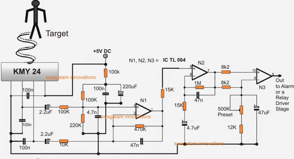
Microwave Fan Wiring Diagram

Microwave Fan Wiring Diagram.

XXX . XXX 4%zero null 0 1 2 3 4 RF & Microwave Power Meter
RF and microwave power measurement and RF and microwave power meters are important elements within the RF and microwave design arena. The output power level of many RF and microwave amplifiers is a critical parameter in the design. As a result it is often necessary to measure the RF power level to ascertain the performance of the item under test.
As a result RF power meters are widely used and RF power measurement techniques are important for any RF design engineer. Different types of RF and microwave power meter are available and some are more suited than others to different types of measurement.
Along with this, it is necessary to know and understand the ways in which power measurements are made, and the errors and methods for minimizing them.

Typical RF / microwave power meter with sensor head
While RF power measurement may be thought is as simply using an RF power meter or a microwave power meter, this is not just the case. Knowing the different measurement techniques, understanding the different types of RF power meter, and ways in which the errors in RF and microwave power measurements can be minimised are all key to making good RF power readings.
RF and microwave power meter basics
There are a number of ways in which RF power (including microwave power) can be measured. There are two main types of RF power meter that are used:- Through-line RF power meters: These RF power meters take a sample of the power flowing along a feed-line and use this to indicate the power level. These through-line RF power meters are used on live systems, such as radio transmitters as a check of the outgoing power. They are normally directional and can be used to check the power travelling in either direction. Measurements made by these RF power meters are frequency insensitive - they measure the total power entering them regardless of frequency (within the overall frequency limitations of the instrument).
- Absorptive RF power meters: As their name implies, these RF power meters absorb the power they measure. Typically they utilise a power sensor that may be one of a variety of types. This generates a signal proportional to the power level entering the sensor. The sensor signal is coupled to the main instrument within the overall RF power meter to process the results and display the reading. Measurements made by these RF power meters are frequency insensitive - they measure the total power entering them regardless of frequency (within the overall frequency limitations of the instrument).
The absorptive RF power meters generally have digital readouts these days. An analogue voltage is generated within the power sensor or power head and this is fed into the main RF power meter unit. With high levels of digital signal processing available these days, many RF power meters contain significant levels of processing and this can enable a variety of signal types to be measured.
When selecting an RF power meter or a microwave power meter, it is important to select the correct type of power sensor. There are a number of different types of power sensor, and these are suited to different types of RF power measurement. Some types of RF power sensor are suited to make measurements of average power, whereas others can make measurements of pulse power or peak envelope power. Further pages of this tutorial address the power measurements - average, pulse power (often termed peak power), and peak envelope power, as well as the different types of sensor that can be used with RF power meters. - Spectrum analysers and other instruments: Instruments such as spectrum analysers have power measurement capabilities within them. These instruments are able to measure the RF power level on a particular frequency, but cannot measure the total power entering on all frequencies. Spectrum analyser RF power measurements used not to be accurate, but with the improvements in their technology, the RF power measurements have far greater levels of accuracy.
Units for RF and microwave power measurements
Power is a measure of energy per unit time and it is typically measured in watts - this is a energy transfer at the rate of one Joule per second.Although the watt is the base measure, often this is preceded by a multiplier as power levels can extend over a vast range. Levels of kilowatts (103 watts), or even megawatts (106 watts) are used in some large power installations, whereas other applications have much lower levels - milliwatts (10-3 watts), or microwatts (10-6 watts) may be found.
In some instances power may be specified in terms of dBW or dBm. These use a the logarithmic decibel scale but related to a given power level.
In itself a decibel is not an absolute level. It is purely a comparison between two levels, and on its own it cannot be used to measure an absolute level. The quantities of dBm and dBW are the most commonly used.
- dBm - This is a power expressed in decibels relative to one milliwatt.
- dBW - This is a power expressed in decibels relative to one watt.
A more extensive table of dBm, dBW and power is given below:
| dBm | dBW | Watts | Terminology |
|---|---|---|---|
| +60 | +30 | 1 000 | 1 kilowatt |
| +50 | +20 | 100 | 100 watts |
| +40 | +10 | 10 | 10 watts |
| +30 | 0 | 1 | 1 watt |
| +20 | -10 | 0.1 | 100 milliwatts |
| +10 | -20 | 0.01 | 10 milliwatts |
| 0 | -30 | 0.001 | 1 milliwatt |
| -10 | -40 | 0.0001 | 100 microwatts |
| -20 | -50 | 0.00001 | 10 microwatts |
| -30 | -60 | 0.000001 | 1 microwatt |
RF average, pulse and peak envelope power measurements
- a summary or overview of the different types power level measurements that can be made - average power, pulse power, peak envelope power, PEP.
When measuring RF and microwave power levels it is necessary to understand the nature of the signal as this can have an impact on the power measurement and the instrument used.Terms including: average power, RF pulse power, RF peak power and peak envelope power, PEP require different measurement techniques and as a result they need different sensor types to measure them.
RF average power
The most obvious way to measure power is to look at the average power. This is defined as the energy transfer rate average over many periods of the RF waveform.The simplest waveform to measure is a continuous wave (CW). As the signal is a single frequency steady state waveform, the average power is obvious.
For other waveforms the averaging parameters may be of greater importance. Take the example of an amplitude modulated waveform. This varies in amplitude over many RF cycles, and the RF power must be averaged over many periods of the modulating waveform to achieve a meaningful result.
To achieve the required results, the averaging period for RF power meters may range from several hundredths of a second up to several seconds. In this way the RF or microwave power meter is able to cater for the majority of waveforms encountered.
RF pulse power or peak power
In a number of applications, it is necessary to measure the power of a pulse of energy. If this were averaged over a long period of time, it would not represent the power of the pulse. In order to measure the power of the pulse itself, a method of defined exactly what must be measured.As the name pulse power implies, the power of the actual pulse itself is measured. For this the pulse width is considered to be the point from which the pulse rises above 50% of its amplitude to the point where it falls below 50% of its amplitude.
As the pulse is likely to include some overshoot and ringing, the most accurate term for the power is the pulse power. Peak power would imply that the value of any overshoot would need to be taken, whereas the actual power measurement required is that of the overall pulse.
Peak envelope power, PEP
For some applications another form of RF power measurement is required. Called peak envelope power, PEP, it is used to measure the power of some varying waveforms.There are many instances where a power measurement that takes the peak of the envelope is needed. Many digitally modulated waveforms may require this, and also transmissions such as AM and Single Sideband may also need this type of RF power measurement.
The envelope power is measured by making the averaging time greater than the period of the modulating waveform, i.e. 1/fm where fm is the maximum frequency component of the modulation waveform.
This means that the averaging time of the RF power measurement must fall within a window:
- It must be large when compared to the period of the highest modulation frequency.
- It must be small compared to the period of the carrier waveform
Summary
Of all the forms of RF power measurement, the average power is the most widely used. It is the most convenient to make, and often expressed the value that needs to be known. However pulse power, sometimes referred to as peak power, and also the peak envelope power also need to be known on many occasions. However the techniques and equipment needed to make peak envelope power and pulse power are different to those needed for average power. Accordingly it is necessary to understand the differences between the different types of RF power measurement and the equipment needed.RF & Microwave Power Sensor Types
RF power is not always easy to measure. There are several methods of measuring RF power, each one having its own advantages and disadvantages. Accordingly the type of RF power sensor used will depend upon the type of signal to be measured. Some types of RF power sensor technology will be more applicable to low powers, others to modulation techniques where the envelope varies and so forth.
Typically an RF or microwave power meter will comprise a unit where all the control and processing circuitry is contained, but the power itself will be detected in what is normally termed a sensor or "head". Thus it may be possible for a power meter to utilise one of a number of power heads according to the exact requirements, particularly with respect to power.
It is important to note that power meters act as a load for the RF power which is absorbed by the head. This high power meters have large loads that can dissipate the required level of power. Alternatively a small portion of the power can be extracted by means of a coupler, or by using a high power attenuator so that the power rating of the RF power meter head is not exceeded.
RF power sensor technologies
The RF power sensors are the key element of any RF power meter, and the choice of the type of sensor will depend of the likely applications that are envisaged. The RF power meter technologies fall into one of two basic categories:- Heat based
- Diode detector based

A typical power meter sensor
Heat based RF power meter sensors
As the name suggests, heat based sensors dissipate the power from a source in a load and then measured the resulting temperature rise.The heat based RF power sensors have the advantage that they are able to measure the true average power as the heat dissipated is the integral of the power input over a period of time. As a result these RF power sensors measure the RF power level independent of the waveform. Thus the measurement is true regardless of whether the waveform is CW, AM, FM, PM, pulsed, has a large crest factor, or consists of some other complex waveform. This is a particular advantage in many instances, especially as QAM, and other forms of phase modulation are being increasingly used and a these do not have a constant envelope.
In view of the time constant with these RF power sensors, they are not suitable for measuring instantaneous values. Where these measurements are required, other types of sensor may be more suitable.
There are two main technologies that are used:
- Thermistor RF power sensors: Thermistor RF power sensors have been widely used for many years and provide a very useful method of enabling high quality RF power measurements to be made. While thermocouple and diode technologies have become more popular in recent years, the thermistor RF power sensors are often the RF power sensor of choice as they enable DC power to be substituted to enable calibration of the system.
The thermistor RF power sensor uses the fact that temperature rise results from dissipating the RF in an RF load. There are two types of sensor that can be used to detect this temperature rise. One is known as a barretter - a thin wire that has a positive temperature coefficient. The other is a thermistor - a semiconductor with a negative temperature coefficient which may typically only be around 0.5 mm in diameter. Today only thermistors are used in RF power sensors.
A balanced bridge technique is normally used. Here the resistance of the thermistor element is maintained at a constant resistance by using a DC bias. As RF power is dissipated in the thermistor tending to lower the resistance, so in turn the bias is reduced to maintain the balance of the bridge. The decrease in bias is then an indication of the power being dissipated.
Today's thermistors sensors contain a second set of thermistors to provide compensation against changes in the ambient temperature that would otherwise offset the readings. - Thermocouple RF power sensors: Thermocouples are widely used these days in RF and microwave power sensors They provide two main advantages:
- They exhibit a higher level of sensitivity than thermistor RF power sensors and can therefore be used for detecting lower power levels. They can easily be made to provide power measurements down to a microwatt.
- Thermocouple RF and microwave power sensors possess a square-law detection characteristic. This results in the input RF power being proportional to DC output voltage from the thermocouple sensor.
- They provide a very rugged power sensor to be made - they are more rugged than thermistors.
The principle of a thermocouple is simple - junctions of dissimilar metals give rise to a small potential when placed at different temperatures. (For a full explanation look at the Radio-Electronics.com page on Thermocouples - check out via the search box).
Modern thermocouples as used in RF and microwave power sensors are typically designed within a single silicon integrated circuit chip. They detect the heat dissipated as a result of the RF signal in the load resistor.
Diode detector based RF power meter sensors
The other form of RF power sensor used in RF power meters, employs diode rectifiers to produce an output. Again RF power seonsors using diodes are designed so that the sensor dissipated the RF power in a load. A diode detector then rectifies the voltage signal appearing across the load, and this can then be used to determine the power level entering the load.Diode based RF power sensors have two major advantages:
- The first is that they are able to measure signals down to very low levels of power. Some of these diode based RF power sensors are able to measure power levels as low as -70 dBm. This is much lower than is possible when using heat based RF power sensors.
- The other advantage of diode based RF power meter sensors, is the fact that they are able to respond more quickly than the heat based varieties. In some older power meters, the output from the diode RF power sensor will be processed in a simple way, but far more sophisticated processing of the readings can be made using digital signal processing techniques. In this way the readings can be processed to give the results in the required format, integrating over time is necessary, or having faster, more instantaneous readings if needed.
Despite the low turn on voltage of the Schottky diode (0.3 volts for silicon), this still limits the lowest signal levels that can be detected - a signal of around -20dBm is required to overcome this voltage. One approach is to AC couple the diode and apply a 0.3 volt bias, but this only increases the sensitivity by around 10 dB as a result of conduction noise and drift introduced by the bias current.
Today, Gallium-Arsenide (GaAs) semiconductor diodes are now often used because they provide superior performance when compared to silicon diodes. The gallium arsenide diodes used in RF power sensors are typically fabricated using planar doped barrier technology, and although the diodes are more costly, they provide significant advantages for power sensors at microwave frequencies.
RF and microwave diode power sensors are often the sensor of choice. The output from the diode can be processed using advanced digital signalling processing. This means that a single sensor is able to provide a large variety of capabilities that would not be possible with heat based sensors. With diodes detecting the envelope, a variety of waveforms can be measured.
Summary
Many RF power meters provide the facility for a variety of radio frequency power sensors to be used dependent upon the exact nature measurements to be made. While the heat based RF power sensors are more applicable to applications where an integrated measurement is required, diode based ones are more suitable where low level or instantaneous measurements are needed. Accordingly it is necessary to choose the sensor dependent upon the foreseen applications.RF & Microwave Power Measurement
- an overview of microwave & RF power measurement techniques - how to make the measurements and the precautions to take.
Microwave and RF power measurements are an important type of measurement that is made within the RF environment. Making accurate RF power measurements not only depends upon having an accurate RF power meter, but also on knowing how to make the measurements in a real environment.There are a number of pointers that can be used to ensure that the RF power measurements that are made are as accurate as possible.
Ensure the RF power measurement type suits the meter
There are many different types of waveform that may need to be measured. Some waveforms have a varying envelope, while others will remain constant. Different power meters sensors operate in different ways and as a result different power sensors are required for different types of RF power measurement.In general the following types of power sensor are available for absorptive power meters:
- Thermistor power sensor: The thermistor RF power sensor is a heat based power sensor and it is used for situations where RF power measurements are required. Being a heat based sensor, it will detect the heat being dissipated over a period of time - typically over tenths of a second. Thermistor power sensors have the advantage that the RF power can be substituted by DC which can be accurately measured using a digital multimeter to give a very accurate calibration of this type of sensor.
- Thermocouple : Thermocouple RF power sensors are also heat based. They are similar in many respects to thermistor types but are able to make RF power measurements down to lower power levels.
- Diode based power sensors: These power sensors act as rectifiers and provide an output of the envelope of the waveform to the meter processor. Using signal processing, these sensors are able to make a variety of RF power measurements including average power, pulse power and peak envelope power. Accordingly these sensors are ideal for making a wide variety of RF power measurements.
Ensure the RF power measurement range suits the meter / sensor
As with any item of test equipment, it is necessary to ensure that the expected readings for the RF power measurements will fall within the range of the meter. It is also best to leave some margin at both top and bottom ends.Often at the bottom end of the range there will be some noise and this adds uncertainty to the RF power measurement. It is often best to leave a margin of around 10 dB at the bottom end.
Also at the top end of the range a margin is useful. Typically leave 3 to 5 dB at the top end of the RF power measurement range. This will leave a margin for power measurement readings coming out larger than expected and it will ensure that the RF power measurements are within the optimum range of the meter.
Ensure the power handling capability cannot be exceeded
Although it really comes under the heading above, it is necessary to ensure that there is no way that excessive power can be applied to the meter while making an RF power measurement. Although the power sensor will be able to tolerate some level of overload when making RF power measurements, it is easy to damage them if too much power is applied.To prevent any possibility of damage, power attenuators may be added to the input of the sensor to ensure that the signal falls within the acceptable range of the sensor.
RF & microwave power measurements: making the right field test choices
The output power of an RF or microwave system is a key determinant of its performance. The two key instruments for making measurements of RF or microwave power in the field are power sensors and spectrum analysers. Each approach has its strengths, and so making a choice of which to use involves trading off between accuracy, frequency range, dynamic range, portability, durability and warm-up time.
Power sensor architecture
A typical power sensor converts an RF/microwave signal to a DC or low-frequency analogue voltage waveform of around 100 nV, which is then amplified and filtered. The first trade-off here is to decide whether to reduce the filter bandwidth to improve measurement sensitivity, or to increase it to improve measurement speed. Whichever choice is made, the resultant signal is then digitised using an analogue-to-digital converter (ADC), so a microprocessor can handle further filtering and time averaging of the waveform.
Figure 1: Block diagram of two approaches to power sensor and power meter architecture (Source: Keysight Technologies)
Different forms of power sensors handle signal processing in different ways. A USB-based power sensor handles its own signal processing (as shown in the black box in Figure 1). If the power sensor has a separate power meter, signal processing is handled in the meter (the red box in Figure 1). Some peak power sensors have additional signal paths to process average and peak measurements separately.Power sensors usually have the highest measurement accuracy but require zeroing and user calibration to correct for frequency response, temperature drift and sensor aging. Keysight power sensors and meters have a 50 MHz reference oscillator for this purpose, whose output power is controlled to ±0.4%.
Thermal power sensors
RF/microwave power sensing is usually done with thermal or diode-based detectors.Thermal sensors respond to the total power in the signal and report its true average power, regardless of modulation, by using the energy of the RF/microwave signal to change one of their electrical properties.
Sensor elements are usually a thermistor or thermocouple.
Thermistors warm up when subject to an RF input, so their resistance drops in a way that can be accurately measured in a bridge circuit. Drawbacks of thermistors include low RF measurement sensitivity (down to approximately -20 dBm), slow operation, sensitivity to ambient temperature, and the need to be connected to a power meter.
In thermocouples, temperature changes generate a voltage change that can be directly measured. Thermocouples are more rugged and less sensitive to ambient temperature than thermistors, making them more useful for field measurements. Their sensitivity is slightly greater, at approximately -35 dBm. Drawbacks include the need for regular calibration for temperature drift and sensor aging, using a reference oscillator
Diode-based power sensors
Diode-based sensors have a wider dynamic range than thermal-based sensors, but they have non-linear characteristics that need careful compensation.Diode-based sensors rectify and filter the input RF/microwave signal using a diode and capacitor, as in Figure 2.

Figure 2: Diode rectification and filtering of an RF input (Source: Keysight Technologies)
The detected output voltage of a diode-based sensor is proportional to the square of the input voltage and therefore linearly related to the input power, within a region from -70 dBm to -20 dBm of input signal. Above 0 dBm, the diode characteristic shifts from a power-to-voltage to linear voltage-to-voltage relationship, through a transition region from –20 dBm to 0 dBm.Drawbacks of diode-based power sensors include the need for access to a reference oscillator for calibration, a warm-up time of up to 30 minutes before use for greatest accuracy, and sensitivity to ESD and mechanical shock.
Putting diode-based power sensors to work
Here are three ways a diode-based power sensor can be used.Measuring the average power of CW signals
With the right signal-processing and compensation techniques, the dynamic range of a diode-based sensor can be more than 90 dB. This is often done by saving correction factors in non-volatile memory to compensate for variations in input power, temperature and frequency.
Measurements in the higher-power transition and linear regions of a diode-based sensor are only accurate for continuous wave (CW) signals. This means they can be used to test frequency sources and the output power from amplifiers. Some diode-based sensors, such as the Keysight E4412/13A, are optimised for CW measurements, for which they have the lowest sensitivity and highest dynamic range of all the sensor types.
Measuring the average power of modulated signals
The correction factors used in the transition and linear region of a diode-based sensor are not accurate enough for the sensor to measure the average power of pulsed and digitally modulated waveforms.
It is possible to attenuate a high-power signal until it can be measured in the square-law region of the sensor. This reduces the sensor’s sensitivity, dynamic range and accuracy. Another approach is to use a sensor with two measurement paths, which can keep the diode operating in its square-law region at all power levels. These wide dynamic-range sensors, such as the Keysight E9300 E-Series, have one measurement path covering -60 to -10 dBm and a second path, with built-in attenuator, to cover -10 to +20 dBm.
**Measuring the peak power of modulated signals **
Measuring the peak power of signals with pulsed and modulated signals requires two levels of signal detection. The modulated signal first has to be detected using the diode sensor and converted to a wideband signal representing the time-varying envelope of the modulated waveform. The second detection occurs when the wideband signal is sampled and processed. Amplitude corrections can then be applied to the samples by adjusting the measured power to match the square-law, transition or linear regions of the diode sensor’s operation.
Tuned receiver power measurements
A spectrum analyser can also be used to measure average power. Handheld instruments such as the Keysight FieldFox can take this measurement with an accuracy that is typically ±0.5 dB across its frequency and temperature range.
Figure 3: The architecture of the tuned receiver used in spectrum analysers (Source: Keysight Technologies)
The front end of the circuit shown in Figure 3 has a down-conversion block using a mixer and local oscillator, plus a bandpass filter before the amplitude detector, to convert the RF input signal to a frequency at which it can be more easily filtered and detected. By sweeping the local oscillator across a frequency range, a spectrum analyser can display the power of a signal as a function of frequency.The ADC samples the down-converted intermediate frequency (IF) for filtering and detection in the digital domain, in this case in two stages. In the first, there’s a bandpass filter with an adjustable bandwidth, which is referred to as its channel or resolution bandwidth (RBW). The next stage is for the signal’s amplitude to be detected and low-pass filtered, using a firmware algorithm that simulates an ideal square-law detector.
One of the advantages of spectrum analysers over power meters is their frequency selectivity, the ability to measure the power in a set RBW. This enables spectrum analysers to measure less powerful signals than power meters, by selecting a narrow RBW. In practice, a power meter may measure down to -70 dBm, while a spectrum analyser like the FieldFox can measure down to -154 dBm/Hz with a dynamic range greater than 105 dB.
RF power meters and spectrum analysers each have advantages and disadvantages. Understanding these should help users choose the approach that will bring them the accuracy, repeatability and traceability they need in their RF and microwave signal power measurements
XXX . XXX 4%zero null 0 1 2 3 4 5^-^ Scope in Space
The Scope In Space project entailed launching one of their Scope Rider oscilloscopes into space on a very high altitude balloon unprotected from the elements, and then allowing it to return to ground on a parachute, whilst monitoring it all the time to see if it failed and still worked after the very rough landing.
Requirements for rugged operationAlthough many oscilloscopes are used in the laboratory and may not need to be nearly as robust as some, there is an increasing requirement for field service equipment at a reasonable cost.
Electronics is now becoming increasingly embedded in all areas of everyday life. Everything from mobile phones and all the infrastructure needed to support them to electronic barriers, remote monitoring and control systems – in fact electronic systems are all around us.
Whilst reliability is normally very good, for initial commissioning of many of these systems, for regular maintenance as well as for repair increasingly complicated testing is required.
Nowadays the field service engineer needs far more than a test meter and to meet this need and as a result, many companies are launching new portable products.
But just how rugged and robust are they? I confess when I was looking to demonstrate robustness of a product I was concerned about even dropping it from a knee height onto carpet. In reality though, equipment needs to be much ore robust than this.
Scope In Space
Rohde & Schwarz wanted to prove the robustness of their new Scope Rider beyond doubt. So a team of engineers from R&S UK contacted a company called a company called SentIntoSpace who arrange and mastermind the balloon launches to send packages into near space – about 30km or more high.
R&S Scope Rider before Launch
They arranged a carrier or housing to take all the tracking equipment as well as protection for the balloon equipment and an almost unprotected area for the scope. It certainly would be open to the elements, water, rain, snow and the like.Video was captured all the time, and position information was relayed to the tracking car.
Scope In Space launch
On the day of the launch the team drove to a local recreation field where the harness was attached to the balloon which was filled with helium so that it could lift the required payload.The payload was then attached and the balloon lifted off. The tracking team were straight on to following the balloon and its path plotted. With wind speeds known and simulations accurate it was due to land in a sparsely populated area.

Scope being launched
With the balloon rising in height towards near-space the temperature was falling and there was obviously the question whether it would survive the ordeal. Temperatures down to -60°C together with rain, wind and snow.Finally when the balloon reached an altitude of 32km above the earth, and the blue of the horizon visible, the atmospheric pressure had fallen so much that the balloon had expanded to its limit (about ten metres in diameter) and it burst. At this altitude the Scope Rider really was a Scope In Space.

R&S Scope Rider in space
After the balloon burst its adventure was not over. When these balloons burst they are so high that they don’t meet much, if any, air resistance and the parachutes would tangle and not work. As a result they enter a free fall phase and reach speeds of up to 55m/s. As its altitude reduced and the air density rose it slowed. Eventually the fall from space was steadied by a parachute, but even with a parachute the final landing would be very rough - a real test for any instrument.Once the scope from space finally landed and it had to be located. With the tracking, this was relatively straightforward.
The scope and its assembly were found in a field in Lincolnshire in the UK - but would the scope work?
On a quick examination the scope was still monitoring and displaying data, none the worse for its trip into space. It truly had been a Scope In Space!
Scope in Space: Scope Rider
The oscilloscope that was sent into space was the R&S Scope Rider. The company describes it as the first handheld oscilloscope with the functionality and touch and feel of a state of the art lab oscilloscope.
R&S Scope Rider oscilloscope
It performs equally well in the lab and in the field. With an acquisition rate of 50,000 waveforms per second, a 10 bit A/D converter developed by Rohde & Schwarz it has a maximum bandwidth of 500 MHz for the analogue input channels.Scope Rider is based on a high performance oscilloscope featuring a precise digital trigger system, 33 automatic measurement functions, mask test and XY diagram mode. In addition, it integrates four further instrument functions: a logic analyser with eight additional digital channels, a protocol analyser with trigger and decoding capability, a data logger and a digital multi meter.
Flash Back concept of Current Sense Transformer Performance
Current transformers are widely used in many areas associated with electronics for monitoring, control and protection.
However the use of current transformers is not well understood generally, and this can lead to poor performance.
Current transformer basics
An ideal current sense transformer has infinite inductance, zero winding resistances, perfect coupling and no parasitics.Secondary current is simply primary current divided by turns ratio.
A real CT shown in Figure 1 has magnetising inductance Lm and parasitic components of leakage inductance Llk, winding resistances Rp and Rs, coupling capacitance Cc, winding self-capacitance Cs and core loss Rloss. Rb is the external ‘burden’ resistor and Rf is secondary impedance reflected to the primary. T1 is an ‘ideal’ transformer. The core can also magnetically saturate. These characteristics, interacting with external components, limit the performance of the CT over frequency and signal amplitude.

Figure 1 CT with parasitics and termination resistor
In operation, sensed current It divides between Rf, and Lm with only the partial current through Rf transforming to current through Rb, indicating a value less than expected. As frequency and Lm impedance reduces, the error increases, counteracted by reducing Rb. Figure 2 shows normalised accuracy for the Murata Power Solutions 53200C 200:1 CT which has Lsec = 8 mH, Cs = 30 pF, Llk = 50 µH and Rs = 34 ohms plotted against Rb. Low frequency bandwidth improvement with decreasing Rb is clear. Another low frequency limit is core saturation, occurring at about 450 milliteslas at 25 Celsius for ferrites. Figure 3 shows that saturation occurs well below the rated bandwidth of 50kHz, again improving with reduced Rb. The maximum current of 10 A within the rated bandwidth is a thermal limit. Note that the ‘diverted’ current into the magnetising inductance causes saturation not the sensed current directly.High frequencies
At high frequencies, Cs and Rloss shunt away current from Rb and the accuracy falls, lower values of Rb again reducing the effect as shown in Figure 2. The rated bandwidth of this part, 500 kHz, is very conservative with a useful response up to several megahertz with low values for Rb.The disadvantage of reducing Rb is that less voltage is developed across it for the same sensed current perhaps making the circuit more prone to noise pick-up and in some situations CT reset time is increased, described later.

Figure 2 Bandwidth Murata 53200CT

Figure 3 Saturation current limit Murata 53200CT
With a square wave sensed current, the ‘diverted’ current into the magnetising inductance increases from zero with time according to Im = Et/Lm where E is the decreasing voltage dropped across Rf as current through it decreases with time. Practically, Vb has an exponential ‘droop’, with reducing Rb or increasing Lsec lessening the effect. Using our Murata CT with a 10 µs pulse, the recommended value for Rb of 200 ohms gives 22.6% droop while Rb = 50 ohms gives just 9.5%.A common sensed waveform has a rising current superimposed on the pulse from magnetising current in a flyback converter transformer or reflected output inductor current in a forward converter. Adding the droop effect to this waveform could leave Vb with a net fall making over-current detection problematic. Also, in current-mode control of switched-mode converters, Vb must have a positive slope to initiate switch turn-off.
Note that the sensed current slope and droop do not arithmetically add because the effects interact giving a net slope less than might be expected. If a net positive slope is required, the effect should be allowed for with a higher value for Lm, lower Rb or larger slope to the sensed current. Remember that the droop is exponential so the slope of Vb tends to a constant, higher value over time.
Pulsed current waveforms
A more realistic waveform for a pulsed current has edge skew and ringing. Predictably, reducing Rb decreases edge skew, the time it takes for the current Is through Lsec to reach its settling value, It/n . Is is driven by the voltage E across Lsec during the skew time according to: dIs/dt=E/LsecE, varying and not very determinate, is the secondary voltage during the skew which depends on the primary compliance voltage and its source impedance. Cs and Lsec have an effect on ringing which is damped by Rb and core losses.
Cc rings with Lsec if the primary and secondary of the transformer have a common ground or have grounds with significant mutual capacitance. Toroidal CTs such as the Murata Power Solutions 5600C series can have lower values of Cc than bobbin-wound types.
Maximum width of pulsed currents is dependent on what droop can be tolerated and eventual saturation of the transformer core. With the 53200C CT, for a sensed current of 10 A, Tonmax is 23, 40 and 63.5 µs for Rb = 200, 100 and 50 ohms respectively before saturation. A rising slope to the sensed current reduces the allowed value. For example with 0.1 A/µs slope on the initial value of 10 A, Tonmax is just 21.1 µs for Rb = 200ohms.
Flux in a CT must be allowed to ‘reset’ between successive pulses otherwise ‘staircase saturation’ of the core can occur. Flux is proportional to current so for maximum speed of reset the magnetising current should decrease as quickly as possible driven by the reverse winding voltage from di/dt = – (E/L).
Rb however limits this voltage to – (Is . Rb). In practice unipolar current waveforms are sensed with the circuit of Figure 4. Here D1 blocks the reset current through Rb so Rr can be a high value giving fast, high voltage reset as long as there is also no reset current path around the transformer primary. However, the reset voltage increases in proportion to Rr and must be kept within the breakdown limit of D1.

Figure 4 Sensing unipolar current waveforms
In real circuits, secondary winding capacitance sinks current and limits the voltage and speed of reset. If all the magnetising energy from the transformer resonantly transfers to Cs, the maximum possible peak voltage Vr is:
V_r = i_m/n √(L_sec/C_s )
For our 5300C CT with for example a primary magnetising current of 2 A peak, maximum secondary reset voltage Vr is 163 VRr could be dispensed with and D1 rated for 163 V plus any cathode voltage. Remember however that this voltage also transforms to the primary winding, in this case, (-) 163/n=-0.815 V
If for example, the CT were in the emitter of a bipolar transistor or source of a low threshold MOSFET, held off by 0V on its base or gate, this voltage could turn on the transistor, possibly with disastrous consequences.
D1 adds to Rb voltage drop reflecting to the primary causing additional magnetising current and reset voltage compared with the bipolar sensing arrangement of Figure 1. A Schottky diode is preferred for D1 for this reason. A fast recovery diode should anyway be used as any recovery current delays reset. Figure 5 shows the simulated resonant reset voltage of the circuit of Figure 4 with Rr = 10 kΩ, a 10 V/ 5 us pulse and with 1N4148 and 1N4003 diodes showing the effect of the long recovery of the 1N4003.

Figure 5 Reset with fast and slow diodes
In summary, effects of the termination impedance and associated components can be tailored to optimise performance for best accuracy over the widest frequency or pulse width range often exceeding the headline specifications of the part.Real time Spectrum Analyzers - what are they?
Spectrum analysers are devices that allow us to look at signals in the frequency domain rather than in the time domain. They are frequency selective devices that can be used to analyse characteristics of wanted signals, such as channel power, bandwidth, level and also unwanted characteristics of signals such as unwanted side band power, spurious or other interference. In many cases a spectrum analyzer can be used to gain more information about a signal such as its phase. Such instruments are normally called vector signal analysers due to this added capability and they are able to perform for example modulation quality or frequency vs time measurements on signals by capturing the signal and post processing it.
In this short article we will discuss the differences between swept and real time spectrum analysers as well as what real time means and what advantages or disadvantages it has over traditional methods.
Traditional Analyzers
A traditional spectrum analyzer sweeps across the spectrum using a heterodyne mixer principle, looking at and capturing small parts of the spectrum at a time and building this into a complete picture over time. Analysing the spectrum from 100MHz to 6GHz, for example, will take some time to accomplish because of the need to sweep over each frequency point to be investigated. For this reason it can be said that a normal swept spectrum analyser, even if the sweep time to cover the spectrum is extremely fast, is blind for the some of the sweep time. If an event occurs in one part of the spectrum when a different part of the spectrum is being examined, the event will be missed.Real-time spectrum analysers have become more interesting in recent years to capture events that have never been possible to see before. Introduced to help identify signals that appear for very short periods of time within a given bandwidth, such as pulsed radar signals or hopping signals, the ultimate aim of real-time spectrum analysis is to capture signals with 100% probability of detection in a way that traditional swept spectrum analyzers are not able to do.
The Real-Time Spectrum Analyser
Compared to a swept spectrum analyser, a real-time analyser works in a different way. The analyser is tuned to a given centre frequency and the signal is sampled in the time domain. The sole purpose of the real-time analyser is to capture every event in a defined bandwidth with no gaps.In the world of oscilloscopes, real time oscilloscopes sample signals fast enough to satisfy Nyquist sampling theorem. These are classed as real time systems. However, in the world of spectrum analysis, real-time does not just mean satisfying Nyquist sampling theorem, but also ensuring that no information is lost in the time taken to process the data. This is one of the main problems with traditional spectrum analysers. Where a signal needs to be processed, there is a gap where no capture is taking place, therefor events that occur in the spectrum are lost.

FSVR Real Time Spectrum Analyzer from Rohde and Schwarz
For a traditional spectrum analyser to perform measurements on modulated signals such as modulation quality (EVM), it must capture (sample) the whole bandwidth of interest at once without sweeping in order to perform the processing. This in itself is a form of real time spectrum analysis, as the signal is sampled in realtime and stored in a capture buffer for offline processing. We call this, "Offline Realtime" and for this reason, all spectrum analysers can be classed as real time instruments when we consider what realtime means in terms of oscilloscope users. What is special about realtime spectrum analysers is that they performs it's processing in an "Online Realtime" mode, meaning no information is missed while data is being processed.The real-time analyser continuously samples data, while in parallel calculating the FFT to recover the frequency spectrum from the time domain data. The FFT process is carried out fast enough to allow overlap of the FFT's, which guarantees 100% power accuracy. Realtime FFT processing of the incoming data stream eliminates blind time, ensuring that every event is detected.
Such analysers can be used to detect very short term events in the frequency domain such as spurs from a swept oscillator, D/A convertor or hopping signals in a radio communications band. Such events would be very difficult to see with a swept analyser.
Realtime spectrum analysers produce much more information that needs to be displayed. It is not uncommon for FFT calculation rates to be in the region of 250,000 FFT's per second. This is more spectrum information than the human eye can interpret and so needs to be displayed in a way for the user to be able to visualise what is happening in the spectrum on screen. For this reason new viewing methods have been developed, such as Persistence Spectrum, Spectrogram and Realtime Spectrum.
Persistence Spectrum
The Persistence Spectrum plots all FFT data produced but with each spectrum being colour coded to determine the probability of signals appearing rather than just the amplitude of a signal. This allows users to see signals, behind signals such as in the screenshots below showing a bluetooth signal hiding behind a Wireless LAN signal, or a CW interferer behind another carrier.

Realtime Spectrogram
With transient signals, information may need to be captured over a long period of time for later analysis. This can be achieved using a Spectrogram. A spectrogram shows each spectrum trace as a colour coded line. The colour of each pixel represents the power of the signal at a specific frequency and time. A real time spectrogram rather than showing swept spectrum information, shows information on each FFT produced to build up a seamless picture of what happens in the spectrum over time.With the above methods showing different aspects of transient signals it can be useful to have a multi-panel display that is able to show the various different displays, giving the user all possible information available to quickly and easily determine properties of the signals under investigation.
Triggering in Realtime Spectrum Analysers
Traditional swept spectrum analysers are known to have very good, accurate triggering systems. However these are normally limited to external triggers, video triggers or IF power triggers. Such triggers although allow the user to perform a measurement on the occurrence of an event, the trigger cannot be used to isolate events in the frequency spectrum.Realtime spectrum analysers are now able to include triggers that are frequency selective. These triggers allow a user to isolate or trigger on an event in one part of the frequency spectrum whilst ignoring events that may occur in another part of the spectrum. This can be extremely useful when trying to identify an intermittent interferer in one part of the spectrum with a constant signal appearing in another part of the spectrum. This type of functionality opens up new possibilities for signal analysis or even combined triggering capability with more complex post processing or signal recording.
Combined Swept and Realtime Spectrum Analysis
A realtime spectrum analyser is an FFT based system. The complete bandwidth it can capture and process in realtime will be limited by its sampling rate, FFT processing power and the RF design of its front end. With current technology realtime spectrum processing is limited to the region of 100MHz or so meaning it is not possible to realtime analyse very large portions of spectrum.For this reason it is important to include and have a system that is able to switch to a swept spectrum mode and is able to use both the heterodyne method to sweep large areas of the spectrum extremely quickly - as a few hundred milliseconds but is then able to switch to its realtime mode to narrow in on an area of spectrum and understand much more about the signal of interest.
Key Points about Realtime Spectrum Analysers Some of the important points about realtime spectrum analyzers are:
- Real time spectrum analysers are FFT based.
- They work in an "online realtime" mode and are able to calculate FFT's without any time gaps.
- They are designed to capture all events that occur in the frequency spectrum for a defined bandwidth.
- They possess improved triggering capability such as being able to trigger on specific events in the frequency domain rather than just time, power or external triggers.
- They provide much more information about what happens to transient signals than can be captured on a swept spectrum analyzer.
++++++++++++++++++++++++++++++++++++++++++++++++++++++++++++++++++++++
SWITCH ( Short Wave Interaction To Couple Highway ) Wonderful Trigger
++++++++++++++++++++++++++++++++++++++++++++++++++++++++++++++++++++++
Thanks For sharing very helpful information
BalasHapusVibrating Fork Level Switch for Solids
Great, Thanks for sharing
BalasHapusWaveguide transition manufacturers