How to Switch a Solenoid?
We turn these solenoids on and off ?
Speed will be important the solenoids have a 5 - 8ms response time.
They have a 24 volt coil pulling 6 watts.
Would a transistor be faster than a relay? Also what about cost?
I would appreciate a part number with your recommendations.
This switch will possible be on continuously so might heat sinks be required if a transistor is suggested?
A transistor would be a little faster than a relay but I don't know if it would really make enough of a difference. The relay appears to draw 250 ma, (1/4 Amp) if it's 6 watts at 24 V.
so the solenoid is good for fairly low pressure as well as typical industrial air pressure supply too.
Almost any switching transistor will work but I would go with something in the TO-220 type packaging just in case it gets a little warm. They dissipate the heat pretty well.
If you are going to use a logic "high" to turn on the circuit, an NPN transistor will do. The solenoid coil would connect between the +24V supply and the collector of the transistor. The emitter would go to ground. Because there is a difference in logic and work voltages, make sure they share the same negative ground and use a 10K resistor in series with the transistor base and your output on the MCU. That will limit any possible feedback from the higher voltage supply. Don't forget to put a clamping diode across the coil of the solenoid, anode side to ground.
Transistors like the 2N3055 or 2N5190 are popular for these applications.
The 3055 is in a TO-3 case while the 5190 is a TO-220 case. Either one is more than capable.
You can also use the smaller transistors like the 2N2222 or 2N3904. We think they are capable of 100mA. (the others are good for much higher currents)
Linear Solenoid Actuator

Another type of electromagnetic actuator that converts an electrical signal into a magnetic field producing a linear motion is called the Linear Solenoid.
The linear solenoid works on the same basic principal as the electromechanical relay seen in the previous tutorial and just like relays, they can also be switched and controlled using transistors or MOSFET’s. A “Linear Solenoid” is an electromagnetic device that converts electrical energy into a mechanical pushing or pulling force or motion.

Linear Solenoid
Linear solenoid’s basically consist of an electrical coil wound around a cylindrical tube with a ferro-magnetic actuator or “plunger” that is free to move or slide “IN” and “OUT” of the coils body. Solenoids can be used to electrically open doors and latches, open or close valves, move and operate robotic limbs and mechanisms, and even actuate electrical switches just by energising its coil.
Solenoids are available in a variety of formats with the more common types being the linear solenoid also known as the linear electromechanical actuator, (LEMA) and the rotary solenoid.
Both types of solenoid, linear and rotational are available as either a holding (continuously energised) or as a latching type (ON-OFF pulse) with the latching types being used in either energised or power-off applications. Linear solenoids can also be designed for proportional motion control were the plunger position is proportional to the power input.
When electrical current flows through a conductor it generates a magnetic field, and the direction of this magnetic field with regards to its North and South Poles is determined by the direction of the current flow within the wire. This coil of wire becomes an “Electromagnet” with its own north and south poles exactly the same as that for a permanent type magnet.
The strength of this magnetic field can be increased or decreased by either controlling the amount of current flowing through the coil or by changing the number of turns or loops that the coil has. An example of an “Electromagnet” is given below.
Magnetic Field produced by a Coil

When an electrical current is passed through the coils windings, it behaves like an electromagnet and the plunger, which is located inside the coil, is attracted towards the centre of the coil by the magnetic flux setup within the coils body, which in turn compresses a small spring attached to one end of the plunger. The force and speed of the plungers movement is determined by the strength of the magnetic flux generated within the coil.
When the supply current is turned “OFF” (de-energised) the electromagnetic field generated previously by the coil collapses and the energy stored in the compressed spring forces the plunger back out to its original rest position. This back and forth movement of the plunger is known as the solenoids “Stroke”, in other words the maximum distance the plunger can travel in either an “IN” or an “OUT” direction, for example, 0 – 30mm.
Linear Solenoid Construction
This type of solenoid is generally called a Linear Solenoid due to the linear directional movement and action of the plunger. Linear solenoids are available in two basic configurations called a “Pull-type” as it pulls the connected load towards itself when energised, and the “Push-type” that act in the opposite direction pushing it away from itself when energised. Both push and pull types are generally constructed the same with the difference being in the location of the return spring and design of the plunger.
Pull-type Linear Solenoid Construction
 Linear solenoids are useful in many applications that require an open or closed (in or out) type motion such as electronically activated door locks, pneumatic or hydraulic control valves, robotics, automotive engine management, irrigation valves to water the garden and even the “Ding-Dong” door bell has one. They are available as open frame, closed frame or sealed tubular types.
Rotary Solenoids
Most electromagnetic solenoids are linear devices producing a linear back and forth force or motion. However, rotational solenoids are also available which produce an angular or rotary motion from a neutral position in either clockwise, anti-cl
0
The power required to activate a high pressure water solenoid will need more than a transistor and 9V battery. I expect the solenoid value <10 Ohms and you need a 100 milliOhm MOSFET.
The 9V battery might be able to supply the base current only but not activate 1 or more solenoids of low DCR.
It is imperative to define load voltage current and make the switch <<5% resistance or so less than the DCR of the solenoid to avoid heat heat rise.
- Define specs before you design.
- Test your assumptions afterwards
- Verify specs.
- Use reverse clamp diode across solenoid to protect driver from Turn off high V.
- Use a low side switch Nch between solenoid and V+
so the solenoid is good for fairly low pressure as well as typical industrial air pressure supply too.
Almost any switching transistor will work but I would go with something in the TO-220 type packaging just in case it gets a little warm. They dissipate the heat pretty well.
If you are going to use a logic "high" to turn on the circuit, an NPN transistor will do. The solenoid coil would connect between the +24V supply and the collector of the transistor. The emitter would go to ground. Because there is a difference in logic and work voltages, make sure they share the same negative ground and use a 10K resistor in series with the transistor base and your output on the MCU. That will limit any possible feedback from the higher voltage supply. Don't forget to put a clamping diode across the coil of the solenoid, anode side to ground.
Transistors like the 2N3055 or 2N5190 are popular for these applications.
The 3055 is in a TO-3 case while the 5190 is a TO-220 case. Either one is more than capable.
You can also use the smaller transistors like the 2N2222 or 2N3904. I think they are capable of 100mA. (the others are good for much higher currents) or in both direA capacitor like that is typically used to provide power for short-term current spikes in the circuit is is directly connected to.
A typical application that needs these type of capacitors (called bypass or filter capacitors) are digital integrated circuits that need a extremely short spike of power every time the state change, but are very low power as long as the state is steady. This spike is caused by internal parasitic capacitances that need to get quickly charged to a different voltage. The inductance of the connection to the power supply might be too high for the power supply to deliver the required current spike, so a capacitor is connected close to the circuit causing the spikes, so that the connection to it has less inductance.
Another use of capacitor for DC is a filter capacitor after an rectifier, to have voltage available even when the AC input is just crossing zero. In that case, I would consider the capacitor part of the power supply, not of the supplied circuit.
In your application, the load is dominated by the coil of the solenoid, which can be modelled as a series circuit of an inductor and a resistor. At turn-on time of the transistor, the inductive behaviour of the coil is dominant, causing a slow rise of the current, and afterwards the pure DC resistance of the coil determines the current, which needs to be constantly supplied while the solenoid is turned on. Neither during turn-on nor in the steady state, a short current spike is consumed, so the capacitor is pointless. Also your LiPo battery does not need a capacitor to deal with zero crossings, as it is a DC source.
Side note: A different situation occurs on AC solenoids with a significant movement of the core: The inductance of an AC solenoid with the core pulled in is significantly higher than at turn-on time. As AC current is determined by the impedance, which might be dominated by the inductance of the solenoid coil, the AC current during pulling can be many times higher than the current in steady active state, up to the destruction of an AC solenoid (due to continuous over-current) if the mechanical movement does not occur, because it is blocked. Of course, an electrolytic cap can not be use to catch the current spike of an AC circuit.c
tions (bi-directional).
to catch the current spike of an AC circuit.c
tions (bi-directional).
 Rotary Solenoid
Rotary solenoids can be used to replace small DC motors or stepper motors were the angular movement is very small with the angle of rotation being the angle moved from the start to the end position.
Commonly available rotary solenoids have movements of 25, 35, 45, 60 and 90o as well as multiple movements to and from a certain angle such as a 2-position self restoring or return to zero rotation, for example 0-to-90-to-0o, 3-position self restoring, for example 0o to +45o or 0o to -45o as well as 2-position latching.
Rotary solenoids produce a rotational movement when either energised, de-energised, or a change in the polarity of an electromagnetic field alters the position of a permanent magnet rotor. Their construction consists of an electrical coil wound around a steel frame with a magnetic disk connected to an output shaft positioned above the coil.
When the coil is energised the electromagnetic field generates multiple north and south poles which repel the adjacent permanent magnetic poles of the disk causing it to rotate at an angle determined by the mechanical construction of the rotary solenoid.
Rotary solenoids are used in vending or gaming machines, valve control, camera shutter with special high speed, low power or variable positioning solenoids with high force or torque are available such as those used in dot matrix printers, typewriters, automatic machines or automotive applications etc.
Rotary Solenoid
Rotary solenoids can be used to replace small DC motors or stepper motors were the angular movement is very small with the angle of rotation being the angle moved from the start to the end position.
Commonly available rotary solenoids have movements of 25, 35, 45, 60 and 90o as well as multiple movements to and from a certain angle such as a 2-position self restoring or return to zero rotation, for example 0-to-90-to-0o, 3-position self restoring, for example 0o to +45o or 0o to -45o as well as 2-position latching.
Rotary solenoids produce a rotational movement when either energised, de-energised, or a change in the polarity of an electromagnetic field alters the position of a permanent magnet rotor. Their construction consists of an electrical coil wound around a steel frame with a magnetic disk connected to an output shaft positioned above the coil.
When the coil is energised the electromagnetic field generates multiple north and south poles which repel the adjacent permanent magnetic poles of the disk causing it to rotate at an angle determined by the mechanical construction of the rotary solenoid.
Rotary solenoids are used in vending or gaming machines, valve control, camera shutter with special high speed, low power or variable positioning solenoids with high force or torque are available such as those used in dot matrix printers, typewriters, automatic machines or automotive applications etc.
Solenoid Switching
Generally solenoids either linear or rotary operate with the application of a DC voltage, but they can also be used with AC sinusoidal voltages by using full wave bridge rectifiers to rectify the supply which then can be used to switch the DC solenoid. Small DC type solenoids can be easily controlled using Transistor or MOSFET switches and are ideal for use in robotic applications.
However, as we saw previously with electromechanical relays, linear solenoids are “inductive” devices so some form of electrical protection is required across the solenoid coil to prevent high back emf voltages from damaging the semiconductor switching device. In this case the standard “Flywheel Diode” is used, but you could equally use a zener diode or small value varistor.
Switching Solenoids using a Transistor

Reducing Energy Consumption
One of the main disadvantages of solenoids and especially the linear solenoid is that they are “inductive devices” made from coils of wire. This means that the solenoid coil converts some of the electrical energy used to operate them into “HEAT” due to the resistance of the wire.
In other words when connected for long periods of time to an electrical supply they get hot!, and the longer the time that the power is applied to a solenoid coil, the hotter the coil will become. Also as the coil heats up, its electrical resistance also changes allowing more current to flow increasing its temperature.
With a continuous voltage input applied to the coil, the solenoids coil does not have the opportunity to cool down because the input power is always on. In order to reduce this self generated heating effect it is necessary to reduce either the amount of time the coil is energised or reduce the amount of current flowing through it.
One method of consuming less current is to apply a suitable high enough voltage to the solenoid coil so as to provide the necessary electromagnetic field to operate and seat the plunger but then once activated to reduce the coils supply voltage to a level sufficient to maintain the plunger in its seated or latched position. One way of achieving this is to connect a suitable “holding” resistor in series with the solenoids coil, for example:
Reducing Solenoid Energy Consumption
 Here, the switch contacts are closed shorting out the resistance and passing the full supply current directly to the solenoid coils windings. Once energised the contacts which can be mechanically connected to the solenoids plunger action open connecting the holding resistor, RH in series with the solenoids coil. This effectively connects the resistor in series with the coil.
By using this method, the solenoid can be connected to its voltage supply indefinitely (continuous duty cycle) as the power consumed by the coil and the heat generated is greatly reduced, which can be up to 85 to 90% using a suitable power resistor. However, the power consumed by the resistor will also generate a certain amount of heat, I2R (Ohm’s Law) and this also needs to be taken into account.
Here, the switch contacts are closed shorting out the resistance and passing the full supply current directly to the solenoid coils windings. Once energised the contacts which can be mechanically connected to the solenoids plunger action open connecting the holding resistor, RH in series with the solenoids coil. This effectively connects the resistor in series with the coil.
By using this method, the solenoid can be connected to its voltage supply indefinitely (continuous duty cycle) as the power consumed by the coil and the heat generated is greatly reduced, which can be up to 85 to 90% using a suitable power resistor. However, the power consumed by the resistor will also generate a certain amount of heat, I2R (Ohm’s Law) and this also needs to be taken into account.
Solenoid Duty Cycle
Another more practical way of reducing the heat generated by the solenoids coil is to use an “intermittent duty cycle”. An intermittent duty cycle means that the coil is repeatedly switched “ON” and “OFF” at a suitable frequency so as to activate the plunger mechanism but not allow it to de-energise during the OFF period of the waveform. Intermittent duty cycle switching is a very effective way to reduce the total power consumed by the coil.
The Duty Cycle (%ED) of a solenoid is the portion of the “ON” time that a solenoid is energised and is the ratio of the “ON” time to the total “ON” and “OFF” time for one complete cycle of operation. In other words, the cycle time equals the switched-ON time plus the switched-OFF time. Duty cycle is expressed as a percentage, for example:

 Then if a solenoid is switched “ON” or energized for 30 seconds and then switched “OFF” for 90 seconds before being re-energized again, one complete cycle, the total “ON/OFF” cycle time would be 120 seconds, (30+90) so the solenoids duty cycle would be calculated as 30/120 secs or 25%. This means that you can determine the solenoids maximum switch-ON time if you know the values of duty cycle and switch-OFF time.
For example, the switch-OFF time equals 15 secs, duty cycle equals 40%, therefore switch-ON time equals 10 secs. A solenoid with a rated Duty Cycle of 100% means that it has a continuous voltage rating and can therefore be left “ON” or continuously energized without overheating or damage.
In this tutorial about solenoids, we have looked at both the Linear Solenoid and the Rotary Solenoid as an electromechanical actuator that can be used as an output device to control a physical process. In the next tutorial we will continue our look at output devices called Actuators, and one that converts a electrical signal into a corresponding rotational movement again using electromagnetism. The type of output device we will look at in the next tutorial is the DC Motor.
Then if a solenoid is switched “ON” or energized for 30 seconds and then switched “OFF” for 90 seconds before being re-energized again, one complete cycle, the total “ON/OFF” cycle time would be 120 seconds, (30+90) so the solenoids duty cycle would be calculated as 30/120 secs or 25%. This means that you can determine the solenoids maximum switch-ON time if you know the values of duty cycle and switch-OFF time.
For example, the switch-OFF time equals 15 secs, duty cycle equals 40%, therefore switch-ON time equals 10 secs. A solenoid with a rated Duty Cycle of 100% means that it has a continuous voltage rating and can therefore be left “ON” or continuously energized without overheating or damage.
In this tutorial about solenoids, we have looked at both the Linear Solenoid and the Rotary Solenoid as an electromechanical actuator that can be used as an output device to control a physical process. In the next tutorial we will continue our look at output devices called Actuators, and one that converts a electrical signal into a corresponding rotational movement again using electromagnetism. The type of output device we will look at in the next tutorial is the DC Motor.
XXX . XXX Input Interfacing Circuits
Input Interfacing allows sensors (Input Transducers) to communicate with PCs and Micro-controllers .

Interfacing is the method of connecting or linking together one device, especially a computer or micro-controller with another allowing us to design or adapt the output and input configurations of the two electronic devices so that they can work together.
But interfacing is more than just using the software program of computers and processors to control something. While computer interfacing uses the unidirectional and bidirectional input and output ports to drive various peripheral devices, many simple electronic circuits can be used to interface to the real world either using mechanical switches as inputs, or individual LEDs as outputs.
 Pushbutton Switch
For an electronic or micro-electronic circuit to be useful and effective, it has to interface with something. Input interface circuits connect electronic circuits such as op-amps, logic gates, etc. to the outside world expanding its capabilities.
Electronic circuits amplify, buffer or process signals from sensors or switches as input information or to control lamps, relays or actuators for output control. Either way, input interfacing circuits convert the voltage and current output of one circuit to the equivalent of another.
Input sensors provide an input for information about an environment. Physical quantities such as temperature, pressure or position that vary slowly or continuously with time can be measured using various sensors and switching devices giving an output signal relative to the physical quantity being measured.
Many of the sensors that we can use in our electronic circuits and projects are resistive in that their resistance changes with the measured quantity. For example, thermistors, strain gauges or light dependant resistors (LDR). These devices are all classed as input devices.
Pushbutton Switch
For an electronic or micro-electronic circuit to be useful and effective, it has to interface with something. Input interface circuits connect electronic circuits such as op-amps, logic gates, etc. to the outside world expanding its capabilities.
Electronic circuits amplify, buffer or process signals from sensors or switches as input information or to control lamps, relays or actuators for output control. Either way, input interfacing circuits convert the voltage and current output of one circuit to the equivalent of another.
Input sensors provide an input for information about an environment. Physical quantities such as temperature, pressure or position that vary slowly or continuously with time can be measured using various sensors and switching devices giving an output signal relative to the physical quantity being measured.
Many of the sensors that we can use in our electronic circuits and projects are resistive in that their resistance changes with the measured quantity. For example, thermistors, strain gauges or light dependant resistors (LDR). These devices are all classed as input devices.
Input Interfacing Circuits
The simplest and most common type of input interfacing device is the push button switch. Mechanical ON-OFF toggle switches, push-button switches, rocker switches, key switches and reed switches, etc. are all popular as input devices because of their low cost and easy of input interfacing to any circuit. Also the operator can change the state of an input simply by operating a switch, pressing a button or moving a magnet over a reed switch.
Input Interfacing A Single Switch
 Switches and push-buttons are mechanical devices that have two or more sets of electrical contacts. When the switch is open or disconnected, the contacts are open circuited and when the switch is closed or operated these contacts are shorted together.
The most common way of input interfacing a switch (or push button) to an electronic circuit is via a pull-up resistor to the supply voltage as shown. When the switch is open, 5 volts, or a logic “1” is given as the output signal. When the switch is closed the output is grounded and 0v, or a logic “0” is given as the output.
Then depending upon the position of the switch, a “high” or a “low” output is produced. A pull-up resistor is necessary to hold the output voltage level at the required value (in this example, +5v) when the switch is open and also to prevent the switch from shorting out the supply when closed.
The size of the pull-up resistor depends on the circuit current when the switch is open. For example, with the switch open, current will flow down through the resistor to the VOUTterminal and from Ohms Law this flow of current will cause a voltage drop to appear across the resistor.
Then if we assume a digital logic TTL gate requires an input “HIGH” current of 60 micro-amps (60uA), this causes a voltage drop across the resistor of: 60uA x 10kΩ = 0.6V, producing an input “HIGH” voltage of 5.0 - 0.6 = 4.4V which is well within the input specifications of a standard digital TTL gate.
A switch or push-button can also be connected in “active high” mode where the switch and resistor are reversed so that the switch is connected between the +5V supply voltage and the output. The resistor, which is now known as a pull-down resistor, is connected between the output and the 0v ground. In this configuration when the switch is open, the output signal, VOUT is at 0v, or logic “0”. When the witch is operated the output goes “HIGH” to the +5 volts supply voltage or logic “1”.
Unlike the pull-up resistor which is used to limit the current, the main purpose of a pull-down resistor is to keep the output terminal, VOUT from floating about by tying it to 0v or ground. As result a much smaller resistor can be used as the voltage drop across it will usually be very small. However, using a too small a pull-down resistor value will result in high currents and high power dissipation in the resistor when the switch is closed or operated.
Switches and push-buttons are mechanical devices that have two or more sets of electrical contacts. When the switch is open or disconnected, the contacts are open circuited and when the switch is closed or operated these contacts are shorted together.
The most common way of input interfacing a switch (or push button) to an electronic circuit is via a pull-up resistor to the supply voltage as shown. When the switch is open, 5 volts, or a logic “1” is given as the output signal. When the switch is closed the output is grounded and 0v, or a logic “0” is given as the output.
Then depending upon the position of the switch, a “high” or a “low” output is produced. A pull-up resistor is necessary to hold the output voltage level at the required value (in this example, +5v) when the switch is open and also to prevent the switch from shorting out the supply when closed.
The size of the pull-up resistor depends on the circuit current when the switch is open. For example, with the switch open, current will flow down through the resistor to the VOUTterminal and from Ohms Law this flow of current will cause a voltage drop to appear across the resistor.
Then if we assume a digital logic TTL gate requires an input “HIGH” current of 60 micro-amps (60uA), this causes a voltage drop across the resistor of: 60uA x 10kΩ = 0.6V, producing an input “HIGH” voltage of 5.0 - 0.6 = 4.4V which is well within the input specifications of a standard digital TTL gate.
A switch or push-button can also be connected in “active high” mode where the switch and resistor are reversed so that the switch is connected between the +5V supply voltage and the output. The resistor, which is now known as a pull-down resistor, is connected between the output and the 0v ground. In this configuration when the switch is open, the output signal, VOUT is at 0v, or logic “0”. When the witch is operated the output goes “HIGH” to the +5 volts supply voltage or logic “1”.
Unlike the pull-up resistor which is used to limit the current, the main purpose of a pull-down resistor is to keep the output terminal, VOUT from floating about by tying it to 0v or ground. As result a much smaller resistor can be used as the voltage drop across it will usually be very small. However, using a too small a pull-down resistor value will result in high currents and high power dissipation in the resistor when the switch is closed or operated.
DIP Switch Input Interfacing
 As well as input interfacing individual push-buttons and rocker switches to circuits, we can also interface several switches together in the form of keypads and DIP switches.
DIP or Dual-in-line Package switches are individual switches that are grouped together as four or eight switches within a single package. This allows DIP switches to be inserted into standard IC sockets or wired directly onto a circuit or breadboard.
Each switch within a DIP switch package normally indicates one of two conditions by its ON-OFF status and a four switch DIP package will have four outputs as shown. Both slide and rotary type DIP switches can be connected together or in combinations of two or three switches which makes input interfacing them to a wide range of circuits very easy.
Mechanical switches are popular because of their low cost and ease of input interfacing. However, mechanical switches have a common problem called “contact bounce”. Mechanical switches consist of two pieces of metal contacts which are pushed together to complete a circuit when you operate the switch. But instead of producing a single clean switching action, the metal parts touch and bounce together inside the body of the switch causing the switching mechanism to open and close several times very quickly.
Because the mechanical switch contacts are designed to open and close quickly, there is very little resistance, called damping to stop the contacts from bouncing about as they make or break. The result is that this bouncing action produces a series of pulses or voltage spikes before the switch makes a solid contact.
As well as input interfacing individual push-buttons and rocker switches to circuits, we can also interface several switches together in the form of keypads and DIP switches.
DIP or Dual-in-line Package switches are individual switches that are grouped together as four or eight switches within a single package. This allows DIP switches to be inserted into standard IC sockets or wired directly onto a circuit or breadboard.
Each switch within a DIP switch package normally indicates one of two conditions by its ON-OFF status and a four switch DIP package will have four outputs as shown. Both slide and rotary type DIP switches can be connected together or in combinations of two or three switches which makes input interfacing them to a wide range of circuits very easy.
Mechanical switches are popular because of their low cost and ease of input interfacing. However, mechanical switches have a common problem called “contact bounce”. Mechanical switches consist of two pieces of metal contacts which are pushed together to complete a circuit when you operate the switch. But instead of producing a single clean switching action, the metal parts touch and bounce together inside the body of the switch causing the switching mechanism to open and close several times very quickly.
Because the mechanical switch contacts are designed to open and close quickly, there is very little resistance, called damping to stop the contacts from bouncing about as they make or break. The result is that this bouncing action produces a series of pulses or voltage spikes before the switch makes a solid contact.
Switch Bounce Waveform
 The problem is that any electronic or digital circuit which the mechanical switch is input interfaced too could read these multiple switch operations as a series of ON and OFF signals lasting several milliseconds instead of just the one intended single and positive switching action.
This multiple switch closing (or opening) action is called Switch Bounce in switches with the same action being called Contact Bounce in relays. Also, as switch and contact bounce occurs during both the opening and closing actions, the resultant bouncing and arcing across the contacts causes wear, increases contact resistance, and lowers the working life of the switch.
However, there are several ways in which we can solve this problem of switch bounce by using some extra circuitry in the form of a debounce circuit to “de-bounce” the input signal. The easiest and most simplest way is to create an RC debounce circuit that allows the switch to charge and discharge a capacitor as shown.
The problem is that any electronic or digital circuit which the mechanical switch is input interfaced too could read these multiple switch operations as a series of ON and OFF signals lasting several milliseconds instead of just the one intended single and positive switching action.
This multiple switch closing (or opening) action is called Switch Bounce in switches with the same action being called Contact Bounce in relays. Also, as switch and contact bounce occurs during both the opening and closing actions, the resultant bouncing and arcing across the contacts causes wear, increases contact resistance, and lowers the working life of the switch.
However, there are several ways in which we can solve this problem of switch bounce by using some extra circuitry in the form of a debounce circuit to “de-bounce” the input signal. The easiest and most simplest way is to create an RC debounce circuit that allows the switch to charge and discharge a capacitor as shown.
RC Switch Debounce Circuit
 With the addition of an extra 100Ω resistor and a 1uF capacitor to the switches input interfacing circuit, the problems of switch bounce can be filtered out. The RC time constant, T is chosen to be longer than the bounce time of the mechanical switching action. An inverting Schmitt-trigger buffer can also be used to produce a sharp output transition from LOW to HIGH, and from HIGH to LOW.
So how does this type of input interfacing circuit work?. Well we saw in the RC Charging tutorial that a capacitor charges up at a rate determined by its time constant, T. This time constant value is measured in terms of T = R*C, in seconds, where R is the value of the resistor in Ohms and C is the value of the capacitor in Farads. This then forms the basis of an RC time constant.
Lets first assume that the switch is closed and the capacitor is fully discharged, then the input to the inverter is LOW and its output is HIGH. When the switch is opened, the capacitor charges up via the two resistors, R1 and R2 at a rate determined by the C(R1+R2) time constant of the RC network.
As the capacitor charges up slowly, any bouncing of the switch contacts are smoothed out by the voltage across the capacitors plates. When the charge on the plates is equal too or greater than the lower input voltage ( VIL ) of the inverter, the inverter changes state and the output becomes LOW. In this simple switch input interfacing example, the RC value is about 10mS giving the switch contacts enough time to settle into their final open state.
When the switch is closed, the now fully charged capacitor will quickly discharge to zero through the 100Ω at a rate determined by the C(R2) time constant changing the state of the inverters output from LOW to HIGH. However, the operation of the switch causes the contacts to bounce about resulting in the capacitor wanting to repeatedly charge up and then discharge rapidly back to zero.
Since the RC charging time constant is ten times longer than the discharge time constant, the capacitor can not charge up fast enough before the switch bounces back to its final closed position as the input rise time has been slowed down, so the inverter keeps the output HIGH. The result is that no matter how much the switch contacts bounce when opening or closing, you will only get a single output pulse from the inverter.
The advantage of this simple switch debounce circuit is hat if the switch contacts bounce too much or fr too long the RC time constant can be increased to compensate. Also remember that this RC time delay means that you will need to wait before you can operate the switch again because if you operate the switch again too soon it will not generate another output signal.
While this simple switch debounce circuit will work for input interfacing single (SPST) switches to electronic and micro controller circuits, the disadvantage of the RC time constant is that it introduces a delay before the next switching action can occur. If the switching action changes state quickly, or multiple keys are operated as on a keypad, then this delay may be unacceptable. One way to overcome this problem and produce a faster input interfacing circuit is to use a cross coupled 2-input NAND or 2-input NOR gates as shown below.
With the addition of an extra 100Ω resistor and a 1uF capacitor to the switches input interfacing circuit, the problems of switch bounce can be filtered out. The RC time constant, T is chosen to be longer than the bounce time of the mechanical switching action. An inverting Schmitt-trigger buffer can also be used to produce a sharp output transition from LOW to HIGH, and from HIGH to LOW.
So how does this type of input interfacing circuit work?. Well we saw in the RC Charging tutorial that a capacitor charges up at a rate determined by its time constant, T. This time constant value is measured in terms of T = R*C, in seconds, where R is the value of the resistor in Ohms and C is the value of the capacitor in Farads. This then forms the basis of an RC time constant.
Lets first assume that the switch is closed and the capacitor is fully discharged, then the input to the inverter is LOW and its output is HIGH. When the switch is opened, the capacitor charges up via the two resistors, R1 and R2 at a rate determined by the C(R1+R2) time constant of the RC network.
As the capacitor charges up slowly, any bouncing of the switch contacts are smoothed out by the voltage across the capacitors plates. When the charge on the plates is equal too or greater than the lower input voltage ( VIL ) of the inverter, the inverter changes state and the output becomes LOW. In this simple switch input interfacing example, the RC value is about 10mS giving the switch contacts enough time to settle into their final open state.
When the switch is closed, the now fully charged capacitor will quickly discharge to zero through the 100Ω at a rate determined by the C(R2) time constant changing the state of the inverters output from LOW to HIGH. However, the operation of the switch causes the contacts to bounce about resulting in the capacitor wanting to repeatedly charge up and then discharge rapidly back to zero.
Since the RC charging time constant is ten times longer than the discharge time constant, the capacitor can not charge up fast enough before the switch bounces back to its final closed position as the input rise time has been slowed down, so the inverter keeps the output HIGH. The result is that no matter how much the switch contacts bounce when opening or closing, you will only get a single output pulse from the inverter.
The advantage of this simple switch debounce circuit is hat if the switch contacts bounce too much or fr too long the RC time constant can be increased to compensate. Also remember that this RC time delay means that you will need to wait before you can operate the switch again because if you operate the switch again too soon it will not generate another output signal.
While this simple switch debounce circuit will work for input interfacing single (SPST) switches to electronic and micro controller circuits, the disadvantage of the RC time constant is that it introduces a delay before the next switching action can occur. If the switching action changes state quickly, or multiple keys are operated as on a keypad, then this delay may be unacceptable. One way to overcome this problem and produce a faster input interfacing circuit is to use a cross coupled 2-input NAND or 2-input NOR gates as shown below.
Switch Debounce with NAND Gates
 This type of switch debounce circuit operates in a very similar way to the SR Flip-flop we looked at in the Sequential Logic section. The two digital logic gates are connected as a pair of cross-coupled NAND gates with active LOW inputs forming a SR Latch circuit as two of the NAND gate inputs are held HIGH (+5v) by the two 1kΩ pull-up resistors as shown.
Also, as the circuit operates as a Set-Reset SR latch, the circuit requires a single-pole double-throw (SPDT) changeover switch rather than a single-pole single-throw (SPST) switch of the previous RC debounce circuit.
When the switch of the cross-coupled NAND debounce circuit is in position A, NAND gate U1 is “set” and the output at Q is HIGH at logic “1”. When the switch is moved to position B, U2 becomes “set” which resets U1. The output at Q is now LOW at logic “0”.
The operating the switch between positions A and B toggles or switches the output at Q from HIGH to LOW or from LOW to HIGH. As the latch requires two switching actions to set and reset it, any bouncing of the switch contacts in either direction for both opening and closing are not seen at the output Q. Also the advantage of this SR latch debounce circuit is that it can provide complementary outputs at Q and Q.
As well as using cross-coupled NAND gates to form a bistable latch input interfacing circuit, we can also use cross-coupled NOR gates by changing the position of the two resistors and reducing their value to 100Ω’s as shown below.
This type of switch debounce circuit operates in a very similar way to the SR Flip-flop we looked at in the Sequential Logic section. The two digital logic gates are connected as a pair of cross-coupled NAND gates with active LOW inputs forming a SR Latch circuit as two of the NAND gate inputs are held HIGH (+5v) by the two 1kΩ pull-up resistors as shown.
Also, as the circuit operates as a Set-Reset SR latch, the circuit requires a single-pole double-throw (SPDT) changeover switch rather than a single-pole single-throw (SPST) switch of the previous RC debounce circuit.
When the switch of the cross-coupled NAND debounce circuit is in position A, NAND gate U1 is “set” and the output at Q is HIGH at logic “1”. When the switch is moved to position B, U2 becomes “set” which resets U1. The output at Q is now LOW at logic “0”.
The operating the switch between positions A and B toggles or switches the output at Q from HIGH to LOW or from LOW to HIGH. As the latch requires two switching actions to set and reset it, any bouncing of the switch contacts in either direction for both opening and closing are not seen at the output Q. Also the advantage of this SR latch debounce circuit is that it can provide complementary outputs at Q and Q.
As well as using cross-coupled NAND gates to form a bistable latch input interfacing circuit, we can also use cross-coupled NOR gates by changing the position of the two resistors and reducing their value to 100Ω’s as shown below.
Switch Debounce with NOR Gates
 The operation of the cross-coupled NOR gate debounce circuit is the same as for the NAND circuit except that the output at Q is HIGH when the switch is in position B and LOW when it is in position A. The reverse of the cross-couple NAND bistable latch.
Then its worth noting that when input interfacing switches to circuits using a NAND or a NOR latch to use as debounce circuits, the NAND configuration requires a LOW or logic “0” input signal to change state, while the NOR configuration requires a HIGH or logic “1” input signal to change state.
The operation of the cross-coupled NOR gate debounce circuit is the same as for the NAND circuit except that the output at Q is HIGH when the switch is in position B and LOW when it is in position A. The reverse of the cross-couple NAND bistable latch.
Then its worth noting that when input interfacing switches to circuits using a NAND or a NOR latch to use as debounce circuits, the NAND configuration requires a LOW or logic “0” input signal to change state, while the NOR configuration requires a HIGH or logic “1” input signal to change state.
Interfacing with Opto Devices
An Optocoupler (or optoisolator) is an electronic component with an LED and photo-sensitive device, such as a photodiode or phototransistor encased in the same package. The Opto-coupler which we look at in a previous tutorial interconnects two separate electrical circuits by means of a light sensitive optical interface. This means that we can effectively interface two circuits of different voltage or power ratings together without one electrically affecting the other.
Optical Switches (or opto-switches) are another type of optical (photo) switching devices which can be used for input interfacing. The advantage here is that the optical switch can be used for input interfacing harmful voltage levels onto the input pins of microcontrollers, PICs and other such digital circuits or for detecting objects using light as the two components are electrically separate but optically coupled providing a high degree of isolation (typically 2-5kV).
Optical switches come in a variety of different types and designs for use in a whole range of interfacing applications. The most common use for opto-switches is in the detection of moving or stationary objects. The phototransistor and photodarlington configurations provide most of the features required for photo-switches and are therefore the most commonly used.
Slotted Optical Switch
 A DC voltage is generally used to drive a light emitting diode (LED) which converts the input signal into infrared light energy. This light is reflected and collected by the phototransistor on the other side of the isolation gap and converted back into an output signal.
For normal opto-switches, the forward voltage drop of the LED is about 1.2 to 1.6 volts at a normal input current of 5 to 20 milliamperes. This gives a series resistor value of between 180 and 470Ω’s.
A DC voltage is generally used to drive a light emitting diode (LED) which converts the input signal into infrared light energy. This light is reflected and collected by the phototransistor on the other side of the isolation gap and converted back into an output signal.
For normal opto-switches, the forward voltage drop of the LED is about 1.2 to 1.6 volts at a normal input current of 5 to 20 milliamperes. This gives a series resistor value of between 180 and 470Ω’s.
Slotted Opto-switch Circuit
 Rotary and slotted disk optical sensors are used extensively in positional encoders, shaft encoders and even the rotary wheel of your computer mouse and as such make excellent input interfacing devices. The rotary disk has a number of slots cut out of an opaque wheel with the number of evenly spaced slots representing the resolution per degree of rotation. Typical encoded discs have a resolution of up to 256 pulses or 8-bits per rotation.
During one revolution of the disk the infrared light from the LED strikes the phototransistor through the slot and then is blocked as the disk rotates, turning the transistor “ON” and then “OFF” each pass of the slot. Resistor R1 set the LED current and the pull-up resistor R2 ensures the supply voltage, Vcc is connected to the input of the Schmitt inverter when the transistor is “OFF” producing a LOW, logic “0” output.
When the disk rotates to an open cut out, the infrared light from the LED strikes the phototransistor and shorts the Collector-to-Emitter terminals to ground producing a LOW input to the Schmitt inverter which in turn outputs a HIGH or logic “1”. If the inverters output was connected to a digital counter or encoder, then it would be possible to determine the shafts position or count the numbers of shaft revolutions per unit time to give the shafts rotations per minute (rpm).
As well as using slotted opto devices as input interfacing switches, there is another type of optical device called a reflective optical sensor which uses an LED and photodevice to detect an object. The reflective opto switch can detect the absence or presence of an object by reflecting (hence its name) the LEDs infrared light of the reflective object being sensed. The basic arrangement of a reflective opto sensor is given below.
Rotary and slotted disk optical sensors are used extensively in positional encoders, shaft encoders and even the rotary wheel of your computer mouse and as such make excellent input interfacing devices. The rotary disk has a number of slots cut out of an opaque wheel with the number of evenly spaced slots representing the resolution per degree of rotation. Typical encoded discs have a resolution of up to 256 pulses or 8-bits per rotation.
During one revolution of the disk the infrared light from the LED strikes the phototransistor through the slot and then is blocked as the disk rotates, turning the transistor “ON” and then “OFF” each pass of the slot. Resistor R1 set the LED current and the pull-up resistor R2 ensures the supply voltage, Vcc is connected to the input of the Schmitt inverter when the transistor is “OFF” producing a LOW, logic “0” output.
When the disk rotates to an open cut out, the infrared light from the LED strikes the phototransistor and shorts the Collector-to-Emitter terminals to ground producing a LOW input to the Schmitt inverter which in turn outputs a HIGH or logic “1”. If the inverters output was connected to a digital counter or encoder, then it would be possible to determine the shafts position or count the numbers of shaft revolutions per unit time to give the shafts rotations per minute (rpm).
As well as using slotted opto devices as input interfacing switches, there is another type of optical device called a reflective optical sensor which uses an LED and photodevice to detect an object. The reflective opto switch can detect the absence or presence of an object by reflecting (hence its name) the LEDs infrared light of the reflective object being sensed. The basic arrangement of a reflective opto sensor is given below.
Reflective Optical Switch
 The phototransistor has a very high “OFF” resistance (dark) and a low “ON” resistance (light), which are controlled by the amount of light striking its base from the LED. If there is no object in front of the sensor then the LEDs infrared light will shine forward as a single beam. When there is an object in close proximity to the sensor the LEDs light is reflected back and detected by the phototransistor. The amount of reflected light sensed by the phototransistor and the degree of transistor saturation will depend on how close or reflective the object is.
Other Types of Opto Devices
As well as using slotted or reflective photoswitches for the input interfacing of circuits, we can also use other types of semiconductor light detectors such as photo resistive light detectors, PN junction photodiodes and even solar cells. All these photo sensitive devices use ambient light such as sunlight or normal room light to activate the device allowing them to be easily interfaced to any type of electronic circuit.
Normal signal and power diodes have their PN junction sealed within a plastic body for both safety and to stop photons of light from hitting it. When a diode is reverse biased it blocks the flow of current, acting like a high resistance open switch. However, if we were to shine a light onto this PN junction the photons of light open up the junction allowing current to flow depending upon the intensity of the light on the junction.
Photodiodes exploit this by having a small transparent window that allows light to strike their PN junction making the photodiode extremely photosensitive. Depending upon the type and amount of semiconductor doping, some photodiodes respond to visible light, and some to infra-red (IR) light. When there is no incident light, the reverse current, is almost negligible and is called the “dark current”. An increase in the amount of light intensity produces an increase in the reverse current.
Then we can see that a photodiode allows reverse current to flow in one direction only which is the opposite to a standard rectifying diode. This reverse current only flows when the photodiode receives a specific amount of light acting as very high impedances under dark conditions and as low impedance devices under bright light conditions and as such of the photodiode can be used in many applications as a high speed light detector.
Interfacing Photodiodes
 In the two basic circuits on the left, the photodiode is simply reverse biased through the resistor with the output voltage signal taken from across the series resistor. This resistor can be of a fixed value, usually between the 10kΩ to 100kΩ range, or as a variable 100kΩ potentiometer as shown. This resistor can be connected between the photodiode and 0v ground, or between the photodiode and the positive Vcc supply.
While photodiodes such as the BPX48 give a very fast response to changes in light level, they can be less sensitive compared to other photo-devices such as the Cadmium Sulphide LDR cell so some form of amplification in the form of a transistor or op-amp may be required. Then we have seen that the photodiode can be used as a variable-resistive device controlled by the amount of light falling on its junction. Photodiodes can be switch from “ON” to “OFF” and back very fast sometimes in nano-seconds or with frequencies above 1MHz and so are commonly used in optical encoders and fibre optic communications.
As well as PN junction photo devices, such as the photodiode or the phototransistor, there are other types of semiconductor light detectors that operate without a PN junction and change their resistive characteristics with changes or variations in light intensity. These devices are called Light Dependant Resistors, or LDR’s.
The LDR, also known as a cadmium-sulphide (CdS) photocell, is a passive device with a resistance that varies with visible light intensity. When no light is present their internal resistance is very high in the order of mega-ohms ( MΩ ). However, when illuminated their resistance falls to below 1kΩ in strong sunlight. Then light dependant resistors operate in a similar fashion to potentiometers but with light intensity controlling their resistive value.
In the two basic circuits on the left, the photodiode is simply reverse biased through the resistor with the output voltage signal taken from across the series resistor. This resistor can be of a fixed value, usually between the 10kΩ to 100kΩ range, or as a variable 100kΩ potentiometer as shown. This resistor can be connected between the photodiode and 0v ground, or between the photodiode and the positive Vcc supply.
While photodiodes such as the BPX48 give a very fast response to changes in light level, they can be less sensitive compared to other photo-devices such as the Cadmium Sulphide LDR cell so some form of amplification in the form of a transistor or op-amp may be required. Then we have seen that the photodiode can be used as a variable-resistive device controlled by the amount of light falling on its junction. Photodiodes can be switch from “ON” to “OFF” and back very fast sometimes in nano-seconds or with frequencies above 1MHz and so are commonly used in optical encoders and fibre optic communications.
As well as PN junction photo devices, such as the photodiode or the phototransistor, there are other types of semiconductor light detectors that operate without a PN junction and change their resistive characteristics with changes or variations in light intensity. These devices are called Light Dependant Resistors, or LDR’s.
The LDR, also known as a cadmium-sulphide (CdS) photocell, is a passive device with a resistance that varies with visible light intensity. When no light is present their internal resistance is very high in the order of mega-ohms ( MΩ ). However, when illuminated their resistance falls to below 1kΩ in strong sunlight. Then light dependant resistors operate in a similar fashion to potentiometers but with light intensity controlling their resistive value.
Interfacing LDR Photoresistors
 Light dependant resistors change their resistive value in proportion to the light intensity. Then LDRs can be used with a series resistor, R to form a voltage divider network across the supply. In the dark the resistance of the LDR is much greater than that of the resistor so by connecting the LDR from supply to resistor or resistor to ground, it can be used as a light detector or as a dark detector as shown.
As LDRs such as the NORP12, produce a variable voltage output relative to their resistive value, they can be used for analogue input interfacing circuits. But LDRs can also be connected as part of a Wheatstone Bridge arrangement as the input of an op-amp voltage comparator or a Schmitt trigger circuit to produce a digital signal for interfacing to digital and microcontroller input circuits.
Simple threshold detectors for either light level, temperature or strain can be used to produce TTL compatible outputs suitable for interfacing directly to a logic circuit or digital input port. Light and temperature level threshold detectors based on an op-amp comparator generate a logic “1” or a logic “0” input whenever the measured level exceeds or falls below the threshold setting.
Light dependant resistors change their resistive value in proportion to the light intensity. Then LDRs can be used with a series resistor, R to form a voltage divider network across the supply. In the dark the resistance of the LDR is much greater than that of the resistor so by connecting the LDR from supply to resistor or resistor to ground, it can be used as a light detector or as a dark detector as shown.
As LDRs such as the NORP12, produce a variable voltage output relative to their resistive value, they can be used for analogue input interfacing circuits. But LDRs can also be connected as part of a Wheatstone Bridge arrangement as the input of an op-amp voltage comparator or a Schmitt trigger circuit to produce a digital signal for interfacing to digital and microcontroller input circuits.
Simple threshold detectors for either light level, temperature or strain can be used to produce TTL compatible outputs suitable for interfacing directly to a logic circuit or digital input port. Light and temperature level threshold detectors based on an op-amp comparator generate a logic “1” or a logic “0” input whenever the measured level exceeds or falls below the threshold setting.
Input Interfacing Summary
As we have seen throughout this tutorial section on input and output devices, there are many different types of sensors which can be used to convert one or more physical properties into an electrical signal that can then be used and processed by a suitable electronic, microcontroller or digital circuit.
The problem is that just about all of the physical properties being measured can not be directly connected to the processing or amplifying circuit. Then some form of input interfacing circuit is required to interface the wide range of different analogue input voltages and currents to a microprocessor digital circuit.
Today with modern PC’s, micro controllers, PIC’s and other such microprocessor based systems, input interfacing circuits allows these low voltage, low power devices to easily communicate with the outside world as many of these PC based devices have built-in input–output ports for transferring data to and from the controllers program and attached switches or sensors.
We have seen that sensors are electrical components that convert one type of property into an electrical signal thereby functioning as input devices. Adding input sensors to an electronic circuit can expand its capabilities by providing information about the surrounding environment. However, sensors can not operate on their own and in the most cases an electrical or electronic circuit called an interface is required.
Then input interfacing circuits allow external devices to exchange signals (data or codes) from either simple switches using switch debounce techniques from a single push button or keyboard for data entry, to input sensors that can detect physical quantities such as light, temperature, pressure, and speed for conversion using analogue-to-digital converters. Then interfacing circuits allow us to do just that.
XXX . XXX 4% zero Interfacing is the method of connecting or linking together one device, especially a computer or micro-controller with another allowing us to design or adapt the output and input configurations of the two electronic devices so that they can work together.
But interfacing is more than just using the software program of computers and processors to control something. While computer interfacing uses the unidirectional and bidirectional input and output ports to drive various peripheral devices, many simple electronic circuits can be used to interface to the real world either using mechanical switches as inputs, or individual LEDs as outputs.
Pushbutton Switch
For an electronic or micro-electronic circuit to be useful and effective, it has to interface with something. Input interface circuits connect electronic circuits such as op-amps, logic gates, etc. to the outside world expanding its capabilities.
Electronic circuits amplify, buffer or process signals from sensors or switches as input information or to control lamps, relays or actuators for output control. Either way, input interfacing circuits convert the voltage and current output of one circuit to the equivalent of another.
Input sensors provide an input for information about an environment. Physical quantities such as temperature, pressure or position that vary slowly or continuously with time can be measured using various sensors and switching devices giving an output signal relative to the physical quantity being measured.
Many of the sensors that we can use in our electronic circuits and projects are resistive in that their resistance changes with the measured quantity. For example, thermistors, strain gauges or light dependant resistors (LDR). These devices are all classed as input devices.
Input Interfacing Circuits
The simplest and most common type of input interfacing device is the push button switch. Mechanical ON-OFF toggle switches, push-button switches, rocker switches, key switches and reed switches, etc. are all popular as input devices because of their low cost and easy of input interfacing to any circuit. Also the operator can change the state of an input simply by operating a switch, pressing a button or moving a magnet over a reed switch.
Input Interfacing A Single Switch
Switches and push-buttons are mechanical devices that have two or more sets of electrical contacts. When the switch is open or disconnected, the contacts are open circuited and when the switch is closed or operated these contacts are shorted together.
The most common way of input interfacing a switch (or push button) to an electronic circuit is via a pull-up resistor to the supply voltage as shown. When the switch is open, 5 volts, or a logic “1” is given as the output signal. When the switch is closed the output is grounded and 0v, or a logic “0” is given as the output.
Then depending upon the position of the switch, a “high” or a “low” output is produced. A pull-up resistor is necessary to hold the output voltage level at the required value (in this example, +5v) when the switch is open and also to prevent the switch from shorting out the supply when closed.
The size of the pull-up resistor depends on the circuit current when the switch is open. For example, with the switch open, current will flow down through the resistor to the VOUTterminal and from Ohms Law this flow of current will cause a voltage drop to appear across the resistor.
Then if we assume a digital logic TTL gate requires an input “HIGH” current of 60 micro-amps (60uA), this causes a voltage drop across the resistor of: 60uA x 10kΩ = 0.6V, producing an input “HIGH” voltage of 5.0 - 0.6 = 4.4V which is well within the input specifications of a standard digital TTL gate.
A switch or push-button can also be connected in “active high” mode where the switch and resistor are reversed so that the switch is connected between the +5V supply voltage and the output. The resistor, which is now known as a pull-down resistor, is connected between the output and the 0v ground. In this configuration when the switch is open, the output signal, VOUT is at 0v, or logic “0”. When the witch is operated the output goes “HIGH” to the +5 volts supply voltage or logic “1”.
Unlike the pull-up resistor which is used to limit the current, the main purpose of a pull-down resistor is to keep the output terminal, VOUT from floating about by tying it to 0v or ground. As result a much smaller resistor can be used as the voltage drop across it will usually be very small. However, using a too small a pull-down resistor value will result in high currents and high power dissipation in the resistor when the switch is closed or operated.
DIP Switch Input Interfacing
As well as input interfacing individual push-buttons and rocker switches to circuits, we can also interface several switches together in the form of keypads and DIP switches.
DIP or Dual-in-line Package switches are individual switches that are grouped together as four or eight switches within a single package. This allows DIP switches to be inserted into standard IC sockets or wired directly onto a circuit or breadboard.
Each switch within a DIP switch package normally indicates one of two conditions by its ON-OFF status and a four switch DIP package will have four outputs as shown. Both slide and rotary type DIP switches can be connected together or in combinations of two or three switches which makes input interfacing them to a wide range of circuits very easy.
Mechanical switches are popular because of their low cost and ease of input interfacing. However, mechanical switches have a common problem called “contact bounce”. Mechanical switches consist of two pieces of metal contacts which are pushed together to complete a circuit when you operate the switch. But instead of producing a single clean switching action, the metal parts touch and bounce together inside the body of the switch causing the switching mechanism to open and close several times very quickly.
Because the mechanical switch contacts are designed to open and close quickly, there is very little resistance, called damping to stop the contacts from bouncing about as they make or break. The result is that this bouncing action produces a series of pulses or voltage spikes before the switch makes a solid contact.
Switch Bounce Waveform
The problem is that any electronic or digital circuit which the mechanical switch is input interfaced too could read these multiple switch operations as a series of ON and OFF signals lasting several milliseconds instead of just the one intended single and positive switching action.
This multiple switch closing (or opening) action is called Switch Bounce in switches with the same action being called Contact Bounce in relays. Also, as switch and contact bounce occurs during both the opening and closing actions, the resultant bouncing and arcing across the contacts causes wear, increases contact resistance, and lowers the working life of the switch.
However, there are several ways in which we can solve this problem of switch bounce by using some extra circuitry in the form of a debounce circuit to “de-bounce” the input signal. The easiest and most simplest way is to create an RC debounce circuit that allows the switch to charge and discharge a capacitor as shown.
RC Switch Debounce Circuit
With the addition of an extra 100Ω resistor and a 1uF capacitor to the switches input interfacing circuit, the problems of switch bounce can be filtered out. The RC time constant, T is chosen to be longer than the bounce time of the mechanical switching action. An inverting Schmitt-trigger buffer can also be used to produce a sharp output transition from LOW to HIGH, and from HIGH to LOW.
So how does this type of input interfacing circuit work?. Well we saw in the RC Charging tutorial that a capacitor charges up at a rate determined by its time constant, T. This time constant value is measured in terms of T = R*C, in seconds, where R is the value of the resistor in Ohms and C is the value of the capacitor in Farads. This then forms the basis of an RC time constant.
Lets first assume that the switch is closed and the capacitor is fully discharged, then the input to the inverter is LOW and its output is HIGH. When the switch is opened, the capacitor charges up via the two resistors, R1 and R2 at a rate determined by the C(R1+R2) time constant of the RC network.
As the capacitor charges up slowly, any bouncing of the switch contacts are smoothed out by the voltage across the capacitors plates. When the charge on the plates is equal too or greater than the lower input voltage ( VIL ) of the inverter, the inverter changes state and the output becomes LOW. In this simple switch input interfacing example, the RC value is about 10mS giving the switch contacts enough time to settle into their final open state.
When the switch is closed, the now fully charged capacitor will quickly discharge to zero through the 100Ω at a rate determined by the C(R2) time constant changing the state of the inverters output from LOW to HIGH. However, the operation of the switch causes the contacts to bounce about resulting in the capacitor wanting to repeatedly charge up and then discharge rapidly back to zero.
Since the RC charging time constant is ten times longer than the discharge time constant, the capacitor can not charge up fast enough before the switch bounces back to its final closed position as the input rise time has been slowed down, so the inverter keeps the output HIGH. The result is that no matter how much the switch contacts bounce when opening or closing, you will only get a single output pulse from the inverter.
The advantage of this simple switch debounce circuit is hat if the switch contacts bounce too much or fr too long the RC time constant can be increased to compensate. Also remember that this RC time delay means that you will need to wait before you can operate the switch again because if you operate the switch again too soon it will not generate another output signal.
While this simple switch debounce circuit will work for input interfacing single (SPST) switches to electronic and micro controller circuits, the disadvantage of the RC time constant is that it introduces a delay before the next switching action can occur. If the switching action changes state quickly, or multiple keys are operated as on a keypad, then this delay may be unacceptable. One way to overcome this problem and produce a faster input interfacing circuit is to use a cross coupled 2-input NAND or 2-input NOR gates as shown below.
Switch Debounce with NAND Gates
This type of switch debounce circuit operates in a very similar way to the SR Flip-flop we looked at in the Sequential Logic section. The two digital logic gates are connected as a pair of cross-coupled NAND gates with active LOW inputs forming a SR Latch circuit as two of the NAND gate inputs are held HIGH (+5v) by the two 1kΩ pull-up resistors as shown.
Also, as the circuit operates as a Set-Reset SR latch, the circuit requires a single-pole double-throw (SPDT) changeover switch rather than a single-pole single-throw (SPST) switch of the previous RC debounce circuit.
When the switch of the cross-coupled NAND debounce circuit is in position A, NAND gate U1 is “set” and the output at Q is HIGH at logic “1”. When the switch is moved to position B, U2 becomes “set” which resets U1. The output at Q is now LOW at logic “0”.
The operating the switch between positions A and B toggles or switches the output at Q from HIGH to LOW or from LOW to HIGH. As the latch requires two switching actions to set and reset it, any bouncing of the switch contacts in either direction for both opening and closing are not seen at the output Q. Also the advantage of this SR latch debounce circuit is that it can provide complementary outputs at Q and Q.
As well as using cross-coupled NAND gates to form a bistable latch input interfacing circuit, we can also use cross-coupled NOR gates by changing the position of the two resistors and reducing their value to 100Ω’s as shown below.
Switch Debounce with NOR Gates
The operation of the cross-coupled NOR gate debounce circuit is the same as for the NAND circuit except that the output at Q is HIGH when the switch is in position B and LOW when it is in position A. The reverse of the cross-couple NAND bistable latch.
Then its worth noting that when input interfacing switches to circuits using a NAND or a NOR latch to use as debounce circuits, the NAND configuration requires a LOW or logic “0” input signal to change state, while the NOR configuration requires a HIGH or logic “1” input signal to change state.
Interfacing with Opto Devices
An Optocoupler (or optoisolator) is an electronic component with an LED and photo-sensitive device, such as a photodiode or phototransistor encased in the same package. The Opto-coupler which we look at in a previous tutorial interconnects two separate electrical circuits by means of a light sensitive optical interface. This means that we can effectively interface two circuits of different voltage or power ratings together without one electrically affecting the other.
Optical Switches (or opto-switches) are another type of optical (photo) switching devices which can be used for input interfacing. The advantage here is that the optical switch can be used for input interfacing harmful voltage levels onto the input pins of microcontrollers, PICs and other such digital circuits or for detecting objects using light as the two components are electrically separate but optically coupled providing a high degree of isolation (typically 2-5kV).
Optical switches come in a variety of different types and designs for use in a whole range of interfacing applications. The most common use for opto-switches is in the detection of moving or stationary objects. The phototransistor and photodarlington configurations provide most of the features required for photo-switches and are therefore the most commonly used.
Slotted Optical Switch
A DC voltage is generally used to drive a light emitting diode (LED) which converts the input signal into infrared light energy. This light is reflected and collected by the phototransistor on the other side of the isolation gap and converted back into an output signal.
For normal opto-switches, the forward voltage drop of the LED is about 1.2 to 1.6 volts at a normal input current of 5 to 20 milliamperes. This gives a series resistor value of between 180 and 470Ω’s.
Slotted Opto-switch Circuit
Rotary and slotted disk optical sensors are used extensively in positional encoders, shaft encoders and even the rotary wheel of your computer mouse and as such make excellent input interfacing devices. The rotary disk has a number of slots cut out of an opaque wheel with the number of evenly spaced slots representing the resolution per degree of rotation. Typical encoded discs have a resolution of up to 256 pulses or 8-bits per rotation.
During one revolution of the disk the infrared light from the LED strikes the phototransistor through the slot and then is blocked as the disk rotates, turning the transistor “ON” and then “OFF” each pass of the slot. Resistor R1 set the LED current and the pull-up resistor R2 ensures the supply voltage, Vcc is connected to the input of the Schmitt inverter when the transistor is “OFF” producing a LOW, logic “0” output.
When the disk rotates to an open cut out, the infrared light from the LED strikes the phototransistor and shorts the Collector-to-Emitter terminals to ground producing a LOW input to the Schmitt inverter which in turn outputs a HIGH or logic “1”. If the inverters output was connected to a digital counter or encoder, then it would be possible to determine the shafts position or count the numbers of shaft revolutions per unit time to give the shafts rotations per minute (rpm).
As well as using slotted opto devices as input interfacing switches, there is another type of optical device called a reflective optical sensor which uses an LED and photodevice to detect an object. The reflective opto switch can detect the absence or presence of an object by reflecting (hence its name) the LEDs infrared light of the reflective object being sensed. The basic arrangement of a reflective opto sensor is given below.
Reflective Optical Switch
The phototransistor has a very high “OFF” resistance (dark) and a low “ON” resistance (light), which are controlled by the amount of light striking its base from the LED. If there is no object in front of the sensor then the LEDs infrared light will shine forward as a single beam. When there is an object in close proximity to the sensor the LEDs light is reflected back and detected by the phototransistor. The amount of reflected light sensed by the phototransistor and the degree of transistor saturation will depend on how close or reflective the object is.
Other Types of Opto Devices
As well as using slotted or reflective photoswitches for the input interfacing of circuits, we can also use other types of semiconductor light detectors such as photo resistive light detectors, PN junction photodiodes and even solar cells. All these photo sensitive devices use ambient light such as sunlight or normal room light to activate the device allowing them to be easily interfaced to any type of electronic circuit.
Normal signal and power diodes have their PN junction sealed within a plastic body for both safety and to stop photons of light from hitting it. When a diode is reverse biased it blocks the flow of current, acting like a high resistance open switch. However, if we were to shine a light onto this PN junction the photons of light open up the junction allowing current to flow depending upon the intensity of the light on the junction.
Photodiodes exploit this by having a small transparent window that allows light to strike their PN junction making the photodiode extremely photosensitive. Depending upon the type and amount of semiconductor doping, some photodiodes respond to visible light, and some to infra-red (IR) light. When there is no incident light, the reverse current, is almost negligible and is called the “dark current”. An increase in the amount of light intensity produces an increase in the reverse current.
Then we can see that a photodiode allows reverse current to flow in one direction only which is the opposite to a standard rectifying diode. This reverse current only flows when the photodiode receives a specific amount of light acting as very high impedances under dark conditions and as low impedance devices under bright light conditions and as such of the photodiode can be used in many applications as a high speed light detector.
Interfacing Photodiodes
In the two basic circuits on the left, the photodiode is simply reverse biased through the resistor with the output voltage signal taken from across the series resistor. This resistor can be of a fixed value, usually between the 10kΩ to 100kΩ range, or as a variable 100kΩ potentiometer as shown. This resistor can be connected between the photodiode and 0v ground, or between the photodiode and the positive Vcc supply.
While photodiodes such as the BPX48 give a very fast response to changes in light level, they can be less sensitive compared to other photo-devices such as the Cadmium Sulphide LDR cell so some form of amplification in the form of a transistor or op-amp may be required. Then we have seen that the photodiode can be used as a variable-resistive device controlled by the amount of light falling on its junction. Photodiodes can be switch from “ON” to “OFF” and back very fast sometimes in nano-seconds or with frequencies above 1MHz and so are commonly used in optical encoders and fibre optic communications.
As well as PN junction photo devices, such as the photodiode or the phototransistor, there are other types of semiconductor light detectors that operate without a PN junction and change their resistive characteristics with changes or variations in light intensity. These devices are called Light Dependant Resistors, or LDR’s.
The LDR, also known as a cadmium-sulphide (CdS) photocell, is a passive device with a resistance that varies with visible light intensity. When no light is present their internal resistance is very high in the order of mega-ohms ( MΩ ). However, when illuminated their resistance falls to below 1kΩ in strong sunlight. Then light dependant resistors operate in a similar fashion to potentiometers but with light intensity controlling their resistive value.
Interfacing LDR Photoresistors
Light dependant resistors change their resistive value in proportion to the light intensity. Then LDRs can be used with a series resistor, R to form a voltage divider network across the supply. In the dark the resistance of the LDR is much greater than that of the resistor so by connecting the LDR from supply to resistor or resistor to ground, it can be used as a light detector or as a dark detector as shown.
As LDRs such as the NORP12, produce a variable voltage output relative to their resistive value, they can be used for analogue input interfacing circuits. But LDRs can also be connected as part of a Wheatstone Bridge arrangement as the input of an op-amp voltage comparator or a Schmitt trigger circuit to produce a digital signal for interfacing to digital and microcontroller input circuits.
Simple threshold detectors for either light level, temperature or strain can be used to produce TTL compatible outputs suitable for interfacing directly to a logic circuit or digital input port. Light and temperature level threshold detectors based on an op-amp comparator generate a logic “1” or a logic “0” input whenever the measured level exceeds or falls below the threshold setting.
Input Interfacing Summary
As we have seen throughout this tutorial section on input and output devices, there are many different types of sensors which can be used to convert one or more physical properties into an electrical signal that can then be used and processed by a suitable electronic, microcontroller or digital circuit.
The problem is that just about all of the physical properties being measured can not be directly connected to the processing or amplifying circuit. Then some form of input interfacing circuit is required to interface the wide range of different analogue input voltages and currents to a microprocessor digital circuit.
Today with modern PC’s, microcontrollers, PIC’s and other such microprocessor based systems, input interfacing circuits allows these low voltage, low power devices to easily communicate with the outside world as many of these PC based devices have built-in input–output ports for transferring data to and from the controllers program and attached switches or sensors.
We have seen that sensors are electrical components that convert one type of property into an electrical signal thereby functioning as input devices. Adding input sensors to an electronic circuit can expand its capabilities by providing information about the surrounding environment. However, sensors can not operate on their own and in the most cases an electrical or electronic circuit called an interface is required.
Then input interfacing circuits allow external devices to exchange signals (data or codes) from either simple switches using switch debounce techniques from a single push button or keyboard for data entry, to input sensors that can detect physical quantities such as light, temperature, pressure, and speed for conversion using analogue-to-digital converters. Then interfacing circuits allow us to do just that.
XXX . XXX 4%zero null output interfacing circuit
Output Interfacing of electronic circuits, PICs and micro-controllers allows them to control the real world by making things move or flash a few lights
 As we saw in the previous input interfacing tutorial, an interface circuit allows one type of circuit to be connected to another type of circuit that may be of a different voltage or current rating.
But as well as interfacing input devices such as switches and sensors we can also interface output devices such as relays, magnetic solenoids and lights. Then interfacing output devices to electronic circuits is known commonly as: Output Interfacing.
Output Interfacing of Electronic circuits and micro-controllers allows them to control the real world by making things move for example, the motors or arms of robots, etc. But output interfacing circuits can also be used to switch things ON or OFF, such as indicators or lights. Then output interface circuits can have a digital output or an analogue output signal.
As we saw in the previous input interfacing tutorial, an interface circuit allows one type of circuit to be connected to another type of circuit that may be of a different voltage or current rating.
But as well as interfacing input devices such as switches and sensors we can also interface output devices such as relays, magnetic solenoids and lights. Then interfacing output devices to electronic circuits is known commonly as: Output Interfacing.
Output Interfacing of Electronic circuits and micro-controllers allows them to control the real world by making things move for example, the motors or arms of robots, etc. But output interfacing circuits can also be used to switch things ON or OFF, such as indicators or lights. Then output interface circuits can have a digital output or an analogue output signal.
 DC Motor is an
Output Device
Digital logic outputs are the most common type of output interfacing signal and the easiest to control. Digital output interfaces convert a signal from a micro-controllers output port or digital circuits into an ON/OFF contact output using relays using the controllers software.
Analogue output interfacing circuits use amplifiers to produce a varying voltage or current signal for speed or positional control type outputs. Pulsed output switching is another type of output control which varies the duty cycle of the output signal for lamp dimming or speed control of a DC motor.
While input interfacing circuits are designed to accept different voltage levels from different types of sensors, output interfacing circuits are required to produce larger current driving capability and/or voltage levels. Voltage levels of the output signals can be increased by providing open-collector (or open-drain) output configurations. That is the collector terminal of a transistor (or the drain terminal of a MOSFET) is normally connected to the load.
The output stages of nearly all micro-controllers, PIC’s or digital logic circuits can either sink or source useful amounts of output current for switching and controlling a large range of output interfacing devices to control the real world. When we talk about sinking and sourcing currents, the output interface can both “give out” (source) a switching current or “absorb” (sink) a switching current. Which means that depending upon how the load is connected to the output interface, a HIGH or LOW output will activate it.
Perhaps the simplest of all output interfacing devices are those used to produce light either as a single ON/OFF indicator or as part of a multi-segment or bar-graph display. But unlike a normal light bulb that can be connected directly to the output of a circuit, LEDs being diodes need a series resistor to limit their forward current.
Output Interfacing Circuits
Light emitting diodes, or LEDs for short, are an excellent low power choice as an output device for many electronic circuits as they can be used to replace high wattage, high temperature filament light bulbs as status indicators. An LED is typically driven by a low voltage, low current supply making them a very attractive component for use in digital circuits. Also, being a solid state device, they can have an operational life expectancy of over 100,000 hours of operation making them an excellent fit and forget component.
Single LED Interface Circuit
 We saw in our Light Emitting Diode Tutorial that an LED is a unidirectional semiconductor device which, when forward biased, that is when its cathode (K) is sufficiently negative with respect to its anode (A), can produce a whole range of coloured output light and brightnesses.
Depending on the semiconductor materials used to construct the LED’s pn-junction, will determine the colour of the light emitted, and their turn-on forward voltage. The most common LED colours being red, green, amber or yellow light.
Unlike a conventional signal diode which has a forward voltage drop of about 0.7 volts for Silicon or about 0.3 volts for Germanium, a light-emitting diode has a greater forward voltage drop than does the common signal diode. But when forward biased produces visible light.
A typical LED when illuminated can have a constant forward voltage drop, VLED of about 1.2 to 1.6 volts and its luminous intensity varies directly with the forward LED current. But as the LED is effectively a “diode” (its arrow like symbol resembles a diode but with little arrows next to the LED symbol to indicate that it emits light), it needs a current limiting resistor to prevent it from shorting out the supply when forward biased.
LEDs can be driven directly from most output interfacing ports as standard LEDs can operate with forward currents of between 5mA and 25mA. A typical coloured LED requires a forward current of around 10 mA to provide a reasonably bright display. So if we assume that a single red LED has a forward voltage drop when illuminated of 1.6 volts, and will be operated by the output port of a 5 volt microcontroller supplying 10mA. Then the value of the current limiting series resistor, RS required is calculated as:
We saw in our Light Emitting Diode Tutorial that an LED is a unidirectional semiconductor device which, when forward biased, that is when its cathode (K) is sufficiently negative with respect to its anode (A), can produce a whole range of coloured output light and brightnesses.
Depending on the semiconductor materials used to construct the LED’s pn-junction, will determine the colour of the light emitted, and their turn-on forward voltage. The most common LED colours being red, green, amber or yellow light.
Unlike a conventional signal diode which has a forward voltage drop of about 0.7 volts for Silicon or about 0.3 volts for Germanium, a light-emitting diode has a greater forward voltage drop than does the common signal diode. But when forward biased produces visible light.
A typical LED when illuminated can have a constant forward voltage drop, VLED of about 1.2 to 1.6 volts and its luminous intensity varies directly with the forward LED current. But as the LED is effectively a “diode” (its arrow like symbol resembles a diode but with little arrows next to the LED symbol to indicate that it emits light), it needs a current limiting resistor to prevent it from shorting out the supply when forward biased.
LEDs can be driven directly from most output interfacing ports as standard LEDs can operate with forward currents of between 5mA and 25mA. A typical coloured LED requires a forward current of around 10 mA to provide a reasonably bright display. So if we assume that a single red LED has a forward voltage drop when illuminated of 1.6 volts, and will be operated by the output port of a 5 volt microcontroller supplying 10mA. Then the value of the current limiting series resistor, RS required is calculated as:
 However, in the E24 (5%) series of preferred resistor values, there is no 340Ω resistor so the nearest preferred value chosen would be 330Ω or 360Ω. In reality depending upon the supply voltage ( VS ) and the required forward current ( IF ), any series resistor value between 150Ω and 750Ω’s would work perfectly well.
Also note that being a series circuit, it does not matter which way around the resistor and LED are connected. However, being unidirectional the LED must be connected the correct way. If you connect the LED the wrong way, it will not be damaged, it just will not illuminate.
However, in the E24 (5%) series of preferred resistor values, there is no 340Ω resistor so the nearest preferred value chosen would be 330Ω or 360Ω. In reality depending upon the supply voltage ( VS ) and the required forward current ( IF ), any series resistor value between 150Ω and 750Ω’s would work perfectly well.
Also note that being a series circuit, it does not matter which way around the resistor and LED are connected. However, being unidirectional the LED must be connected the correct way. If you connect the LED the wrong way, it will not be damaged, it just will not illuminate.
Multi LED Interface Circuit
 As well as using single LEDs (or lamps) for output interfacing circuits, we can also connect two or more LEDs together and power them from the same output voltage for use in optoelectronic circuits and displays.
Connecting together two or more LEDs in series is no different from using a single LED as we saw above, but this time we need to take into account the extra forward voltage drops, VLED of the additional LEDs in the series combination.
For example, in our simple LED output interfacing example above we said that the forward voltage drop of the LED was 1.6 volts. If we use three LEDs in series then the total voltage drop across all three would be 4.8 (3 x 1.6) volts. Then our 5 volt supply could just about be used but it would be better to use a higher 6 volt or 9 volt supply instead to power the three LEDs.
Assuming a supply of 9.0 volts at 10mA (as before), the value of the series current limiting resistor, RS required is calculated as: RS = (9 - 4.8)/10mA = 420Ω. Again in the E24 (5%) series of preferred resistor values, there is no 420Ω resistor so the nearest preferred value chosen would be 430Ω’s.
Being low voltage, low current devices, LEDs are ideal as status indicators which can be driven directly from the output ports of micro-controller and digital logic gates or systems. Micro-controller ports and TTL logic gates have the ability to either sink or source current and therefore can light an LED either by grounding the cathode (if the anode is tied to +5v) or by applying +5v to the anode (if the cathode is grounded) through an appropriate series resistor as shown.
As well as using single LEDs (or lamps) for output interfacing circuits, we can also connect two or more LEDs together and power them from the same output voltage for use in optoelectronic circuits and displays.
Connecting together two or more LEDs in series is no different from using a single LED as we saw above, but this time we need to take into account the extra forward voltage drops, VLED of the additional LEDs in the series combination.
For example, in our simple LED output interfacing example above we said that the forward voltage drop of the LED was 1.6 volts. If we use three LEDs in series then the total voltage drop across all three would be 4.8 (3 x 1.6) volts. Then our 5 volt supply could just about be used but it would be better to use a higher 6 volt or 9 volt supply instead to power the three LEDs.
Assuming a supply of 9.0 volts at 10mA (as before), the value of the series current limiting resistor, RS required is calculated as: RS = (9 - 4.8)/10mA = 420Ω. Again in the E24 (5%) series of preferred resistor values, there is no 420Ω resistor so the nearest preferred value chosen would be 430Ω’s.
Being low voltage, low current devices, LEDs are ideal as status indicators which can be driven directly from the output ports of micro-controller and digital logic gates or systems. Micro-controller ports and TTL logic gates have the ability to either sink or source current and therefore can light an LED either by grounding the cathode (if the anode is tied to +5v) or by applying +5v to the anode (if the cathode is grounded) through an appropriate series resistor as shown.
Digital Output Interfacing an LED
 The output interfacing circuits above work fine for one or more series LEDs, or for any other device whose current requirements are less than 25 mA (the maximum LED forward current). But what happens if the output drive current is insufficient to operate an LED or we wish to operate or switch a load with a higher voltage or current rating such as a 12v filament lamp. The answer is to use an additional switching device such as a transistor, mosfet or a relay as shown.
Output Interfacing High Current Loads
 Common output interfacing devices, such as motors, solenoids and lamps require large currents so they are best controlled or driven by a transistor switch arrangement as shown. That way the load, (lamp or motor) can not overload the output circuit of the switching interface or controller.
Transistor switches are very common and very useful for switching high power loads or for the output interfacing of different power supplies. They can also be switched “ON” and “OFF” several times a second if required, as in pulse width modulation, PWM circuits. But there are a few things we need to consider first about using transistor as switches.
The current flowing into the base-emitter junction is used to control the larger current flowing from the collector to the emitter. Therefore, if no current flows into the base terminal, then no current flows from the collector to the emitter (or through the load connected to the collector), then the transistor is said to be fully-OFF (cut-off).
Switching the transistor fully-ON (saturation), the transistor switch effectively acts as a closed switch, that is its collector voltage is at the same voltage as its emitter voltage. But being a solid state device, even when saturated, there will always be a small voltage drop across the transistors terminals, called VCE(SAT). This voltage ranges from about 0.1 to 0.5 volts depending upon the transistor.
Also, as the transistor will be switched fully-ON, the load resistance will limit the transistors collector current IC to the actual current required by the load (in our case, the current through the lamp). Then too much base current can overheat and damage the switching transistor which somewhat defeats the objective of using a transistor which is to control a bigger load current with a smaller one. Therefore, a resistor is required to limit the base current, IB.
The basic output interfacing circuit using a single switching transistor to control a load is shown below. Note that it is usual to connect a free-wheeling diode, also known as a flywheel diode or back-emf suppression diode such as a 1N4001 or 1N4148 to protect the transistor from any back emf voltages generated across inductive loads such as relays, motors and solenoids, etc. when their current is switched off by the transistor.
Common output interfacing devices, such as motors, solenoids and lamps require large currents so they are best controlled or driven by a transistor switch arrangement as shown. That way the load, (lamp or motor) can not overload the output circuit of the switching interface or controller.
Transistor switches are very common and very useful for switching high power loads or for the output interfacing of different power supplies. They can also be switched “ON” and “OFF” several times a second if required, as in pulse width modulation, PWM circuits. But there are a few things we need to consider first about using transistor as switches.
The current flowing into the base-emitter junction is used to control the larger current flowing from the collector to the emitter. Therefore, if no current flows into the base terminal, then no current flows from the collector to the emitter (or through the load connected to the collector), then the transistor is said to be fully-OFF (cut-off).
Switching the transistor fully-ON (saturation), the transistor switch effectively acts as a closed switch, that is its collector voltage is at the same voltage as its emitter voltage. But being a solid state device, even when saturated, there will always be a small voltage drop across the transistors terminals, called VCE(SAT). This voltage ranges from about 0.1 to 0.5 volts depending upon the transistor.
Also, as the transistor will be switched fully-ON, the load resistance will limit the transistors collector current IC to the actual current required by the load (in our case, the current through the lamp). Then too much base current can overheat and damage the switching transistor which somewhat defeats the objective of using a transistor which is to control a bigger load current with a smaller one. Therefore, a resistor is required to limit the base current, IB.
The basic output interfacing circuit using a single switching transistor to control a load is shown below. Note that it is usual to connect a free-wheeling diode, also known as a flywheel diode or back-emf suppression diode such as a 1N4001 or 1N4148 to protect the transistor from any back emf voltages generated across inductive loads such as relays, motors and solenoids, etc. when their current is switched off by the transistor.
Basic Transistor Switch Circuit
 Lets assume we wish to control the operation of a 5 watt filament lamp connected to a 12 volt supply using the output of a TTL 5.0v digital logic gate via a suitable output interfacing transistor switch circuit. If the DC current gain (the ratio between collector (output) and base (input) current), beta (β) of the transistor is 100 (you can find this Beta or hFE value from the datasheet of the transistor you use) and its VCE saturation voltage when fully-ON is 0.3 volts, what will be the value of the base resistor, RB required to limit the collector current.
The transistors collector current, IC will be the same value of current that follows through the filament lamp. If the power rating of the lamp is 5 watts, then the current when fully-ON will be:
Lets assume we wish to control the operation of a 5 watt filament lamp connected to a 12 volt supply using the output of a TTL 5.0v digital logic gate via a suitable output interfacing transistor switch circuit. If the DC current gain (the ratio between collector (output) and base (input) current), beta (β) of the transistor is 100 (you can find this Beta or hFE value from the datasheet of the transistor you use) and its VCE saturation voltage when fully-ON is 0.3 volts, what will be the value of the base resistor, RB required to limit the collector current.
The transistors collector current, IC will be the same value of current that follows through the filament lamp. If the power rating of the lamp is 5 watts, then the current when fully-ON will be:
 As IC is equal to the lamp (load) current, the transistors base current will be relative to the current gain of the transistor as IB = IC/β. The current gain was given previously as: β = 100, therefore the minimum base current IB(MIN) is calculated as:
 Having found the value of base current required, we now need to calculate the maximum value of the base resistor, RB(MAX). The information given stated that the base of the transistor was to be controlled from the 5.0v output voltage (Vo) of a digital logic gate. If the base-emitter forward bias voltage is 0.7 volts, the the value of RB is calculated as:
 Then when the output signal from the logic gate is LOW (0v), no base current flows and the transistor is fully-off, that is no current flows through the 1kΩ resistor. When the output signal from the logic gate is HIGH (+5v), the base current is 4.27mA and turns ON the transistor putting 11.7V across the filament lamp. Base resistor RB will dissipate less than 18mW when conducting 4.27mA, so a 1/4W resistor will work.
Note that when using a transistor as a switch in an output interfacing circuit, a good rule of thumb is to choose a base resistor, RB value so that the base drive current IB is approximately 5% or even 10% of the required load current, IC to help drive the transistor well into its saturation region thereby minimizing VCE and power loss.
Also, for a quicker calculation of the resistor values and to reduce the maths a little, you could ignore the 0.1 to 0.5 voltage drop across the collector emitter junction and the 0.7 volt drop across the base emitter junction if you wanted to in your calculations. The resulting approximate value will be close enough to the actual calculated value anyway.
Single power transistor switching circuits are very useful for controlling low power devices, such as filament lamps or for switching relays which can be used to switch much higher power devices, for example, motors and solenoids.
But relays are large, bulky electromechanical devices that can be expensive or take up a lot of room on a circuit board when being used to output interface an 8-port micro-controller for instance.
One way to over come this and switch heavy current devices directly from the output pins of a micro-controller, PIC or digital circuit, is to use a darlington pair configuration formed from two transistors.
One of the main disadvantages of power transistors when used as output interfacing devices is that their current gain, (β) especially at switching high currents, can be too low. As little as 10. To overcome this problem and to reduce the value of the base current required is to use two transistors in a Darlington configuration.
Then when the output signal from the logic gate is LOW (0v), no base current flows and the transistor is fully-off, that is no current flows through the 1kΩ resistor. When the output signal from the logic gate is HIGH (+5v), the base current is 4.27mA and turns ON the transistor putting 11.7V across the filament lamp. Base resistor RB will dissipate less than 18mW when conducting 4.27mA, so a 1/4W resistor will work.
Note that when using a transistor as a switch in an output interfacing circuit, a good rule of thumb is to choose a base resistor, RB value so that the base drive current IB is approximately 5% or even 10% of the required load current, IC to help drive the transistor well into its saturation region thereby minimizing VCE and power loss.
Also, for a quicker calculation of the resistor values and to reduce the maths a little, you could ignore the 0.1 to 0.5 voltage drop across the collector emitter junction and the 0.7 volt drop across the base emitter junction if you wanted to in your calculations. The resulting approximate value will be close enough to the actual calculated value anyway.
Single power transistor switching circuits are very useful for controlling low power devices, such as filament lamps or for switching relays which can be used to switch much higher power devices, for example, motors and solenoids.
But relays are large, bulky electromechanical devices that can be expensive or take up a lot of room on a circuit board when being used to output interface an 8-port micro-controller for instance.
One way to over come this and switch heavy current devices directly from the output pins of a micro-controller, PIC or digital circuit, is to use a darlington pair configuration formed from two transistors.
One of the main disadvantages of power transistors when used as output interfacing devices is that their current gain, (β) especially at switching high currents, can be too low. As little as 10. To overcome this problem and to reduce the value of the base current required is to use two transistors in a Darlington configuration.
Darlington Transistor Configuration
 Darlington transistor configurations can be made from two NPN or two PNP transistors connected together or as a ready made Darlington device such as the 2N6045 or the TIP100 which integrates both transistors and some resistors, to assist in rapid turn-off, within a single TO-220 package for switching applications.
In this darlington configuration, transistor, TR1 is the control transistor and is used to control the conduction of the power switching transistor TR2. The input signal applied to the base of transistor TR1 controls the base current of transistor TR2. The Darlington arrangement, whether individual transistors or as a single package has the same three leads: Emitter (E), Base (B) and Collector (C).
Darlington transistor configurations can have DC current gains (that is the ratio between collector (output) and base (input) current) of several hundred to several thousand depending upon the transistors used. Then it would be possible to control our filament lamp example above with a base current of only a few micro-amperes, (uA) as the collector current, β1IB1 of the first transistor becomes the base current of the second transistor.
Then the current gain of TR2 will be β1β2IB1 as the two gains are multiplied together as βT = β1×β2. In other words, a pair of bipolar transistors combined together to make a single Darlington transistor pair will have their current gains multiplied together.
So by choosing suitable bipolar transistors and with the correct biasing, double emitter follower darlington configurations can be regarded as a single transistor with a very high value of β and consequently a high input impedance into the thousands of ohms.
Fortunately for us, someone has already put several darlington transistor configurations into a single 16-pin IC package making it easy for us to output interface a whole range of devices.
Darlington transistor configurations can be made from two NPN or two PNP transistors connected together or as a ready made Darlington device such as the 2N6045 or the TIP100 which integrates both transistors and some resistors, to assist in rapid turn-off, within a single TO-220 package for switching applications.
In this darlington configuration, transistor, TR1 is the control transistor and is used to control the conduction of the power switching transistor TR2. The input signal applied to the base of transistor TR1 controls the base current of transistor TR2. The Darlington arrangement, whether individual transistors or as a single package has the same three leads: Emitter (E), Base (B) and Collector (C).
Darlington transistor configurations can have DC current gains (that is the ratio between collector (output) and base (input) current) of several hundred to several thousand depending upon the transistors used. Then it would be possible to control our filament lamp example above with a base current of only a few micro-amperes, (uA) as the collector current, β1IB1 of the first transistor becomes the base current of the second transistor.
Then the current gain of TR2 will be β1β2IB1 as the two gains are multiplied together as βT = β1×β2. In other words, a pair of bipolar transistors combined together to make a single Darlington transistor pair will have their current gains multiplied together.
So by choosing suitable bipolar transistors and with the correct biasing, double emitter follower darlington configurations can be regarded as a single transistor with a very high value of β and consequently a high input impedance into the thousands of ohms.
Fortunately for us, someone has already put several darlington transistor configurations into a single 16-pin IC package making it easy for us to output interface a whole range of devices.
The ULN2003A Darlington Transistor Array
The ULN2003A is a inexpensive unipolar darlington transistor array with high efficiency and low power consumption making it extremely useful output interfacing circuit for driving a wide range of loads including solenoids, relays DC Motor’s and LED displays or filament lamps directly from the ports of micro-controllers, PIC’s or digital circuits.
The family of darlington arrays consist of the ULN2002A, ULN2003A and the ULN2004A which are all high voltage, high current darlington arrays each containing seven open collector darlington pairs within a single IC package. The ULN2803 Darlington Driver is also available which contains eight darlington pairs instead of seven.
Each isolated channel of the array is rated at 500mA and can withstand peak currents of up to 600mA making it ideal for controlling small motors or lamps or the gates and bases of high power transistors. Additional suppression diodes are included for inductive load driving and the inputs are pinned opposite the outputs to simplify the connections and board layout.
ULN2003 Darlington Transistor Array
 The ULN2003A Darlington driver has an extremely high input impedance and current gain which can be driven directly from either a TTL or +5V CMOS logic gate. For +15V CMOS logic use the ULN2004A and for higher switching voltages up to 100V it is better to use the SN75468 Darlington array.
If more switching current capability is required then both the Darlington pairs inputs and outputs can be paralleled together for higher current capability. For example, input pins 1 and 2 connected together and output pins 16 and 15 connected together to switch the load.
The ULN2003A Darlington driver has an extremely high input impedance and current gain which can be driven directly from either a TTL or +5V CMOS logic gate. For +15V CMOS logic use the ULN2004A and for higher switching voltages up to 100V it is better to use the SN75468 Darlington array.
If more switching current capability is required then both the Darlington pairs inputs and outputs can be paralleled together for higher current capability. For example, input pins 1 and 2 connected together and output pins 16 and 15 connected together to switch the load.
Power MOSFET Interfacing Circuits
As well as using single transistors or Darlington pairs, power MOSFETs can also be used to switch medium power devices. Unlike the bipolar junction transistor, BJT which requires a base current to drive the transistor into saturation, the MOSFET switch takes virtually no current as the gate terminal is isolated from the main current carrying channel.
Basic MOSFET Switch Circuit
 N-channel, enhancement-mode (normally-off) power MOSFETs, (eMOSFET) with its positive threshold voltage and extremely high input impedance, makes it an ideal device for direct interfacing to micro-controllers, PICs and digital logic circuits that are capable of producing a positive output as shown.
MOSFET switches are controlled by a gate input signal and because of the extremely high input (gate) resistance of the MOSFET, we can parallel, almost without limit, many power MOSFETs together until we achieve the power handling capabilities of the connected load.
In the N-channel enhancement type MOSFET, the device is cut-off (Vgs = 0) and the channel is closed acting like a normally open switch. When a positive bias voltage is applied to the gate, current flows through the channel. The amount of current depends upon the gate bias voltage, Vgs. In other words, to operate the MOSFET in its saturation region, the gate-to-source voltage must be sufficient to maintain the required drain and therefore the load current.
As discussed previously, n-channel eMOSFETS are driven by a voltage applied between the gate and source so adding a zener diode across the MOSFETs gate-to-source junction as shown, serves to protect the transistor from excessive positive or negative input voltages such as those for example, generated from a saturated op-amp comparator output. The zener clamps the positive gate voltage and acts as a conventional diode which begins to conduct one the gate voltage reaches –0.7V, keeping the gate terminal well away from its reverse breakdown voltage limit.
N-channel, enhancement-mode (normally-off) power MOSFETs, (eMOSFET) with its positive threshold voltage and extremely high input impedance, makes it an ideal device for direct interfacing to micro-controllers, PICs and digital logic circuits that are capable of producing a positive output as shown.
MOSFET switches are controlled by a gate input signal and because of the extremely high input (gate) resistance of the MOSFET, we can parallel, almost without limit, many power MOSFETs together until we achieve the power handling capabilities of the connected load.
In the N-channel enhancement type MOSFET, the device is cut-off (Vgs = 0) and the channel is closed acting like a normally open switch. When a positive bias voltage is applied to the gate, current flows through the channel. The amount of current depends upon the gate bias voltage, Vgs. In other words, to operate the MOSFET in its saturation region, the gate-to-source voltage must be sufficient to maintain the required drain and therefore the load current.
As discussed previously, n-channel eMOSFETS are driven by a voltage applied between the gate and source so adding a zener diode across the MOSFETs gate-to-source junction as shown, serves to protect the transistor from excessive positive or negative input voltages such as those for example, generated from a saturated op-amp comparator output. The zener clamps the positive gate voltage and acts as a conventional diode which begins to conduct one the gate voltage reaches –0.7V, keeping the gate terminal well away from its reverse breakdown voltage limit.
MOSFETs and Open-collector Gates
 Output interfacing a power MOSFET from TTL poses a problem when we use gates and drivers with open-collector outputs as the logic gate may not always give us the required VGS output. One way to overcome this problem is to use a pull-up resistor as shown.
The pull-up resistor is connected between the TTL supply rail and the logic gates output which is connected to the MOSFETs gate terminal. When the TTL logic gates output is at logic level “0” (LOW), the MOSFET is “OFF” and when the logic gates output is at logic level “1” (HIGH), the resistor pulls the gate voltage up to the +5v rail.
With this pull-up resistor arrangement, we can fully switch the MOSFET “ON” by tying its gate voltage to the upper supply rail as shown.
Output interfacing a power MOSFET from TTL poses a problem when we use gates and drivers with open-collector outputs as the logic gate may not always give us the required VGS output. One way to overcome this problem is to use a pull-up resistor as shown.
The pull-up resistor is connected between the TTL supply rail and the logic gates output which is connected to the MOSFETs gate terminal. When the TTL logic gates output is at logic level “0” (LOW), the MOSFET is “OFF” and when the logic gates output is at logic level “1” (HIGH), the resistor pulls the gate voltage up to the +5v rail.
With this pull-up resistor arrangement, we can fully switch the MOSFET “ON” by tying its gate voltage to the upper supply rail as shown.
Output Interfacing Motors
We have seen that we can use both bipolar junction transistors or MOSFETs as part of an output interfacing circuit to control a whole range of devices. One common output device is the DC motor which creates a rotational movement. There are hundreds of ways motors and stepper motors can be interfaced to micro-controllers, PICs and digital circuits using a single transistor, darlington transistor or MOSFET.
The problem is that motors are electromechanical devices that use magnetic fields, brushes and coils to create the rotational movement and because of this, motors, and especially cheap toy or computer fan motors generate a lot of “electrical noise” and “voltage spikes” which can damage the switching transistor.
This motor generated electrical noise and over voltage can be reduced by connecting a free wheel diode or non-polarised suppression capacitor across the motors terminals. But one simple way of preventing the electrical noise and reverse voltages from affecting semiconductor transistor switches or the output ports of micro-controllers is to use separate power supplies for the control and motor via a suitable relay.
A typical connection diagram for output interfacing an electromechanical relay to a DC motor is shown below.
ON/OFF DC Motor Control
 The NPN transistor is used as tn ON-OFF switch to provide the desired current to the relay coil. The freewheeling diode is required, the same as above, as the current flowing through the inductive coil when de-energised cannot instantaneously reduced to zero. When the input to the base is set HIGH, the transistor is switched “ON”. Current flows through the relay coil and its contacts close driving the motor.
When the input to the transistors base is LOW, the transistor is switched “OFF” and the motor stops as the relay contacts are now open. Any back-emf generated by deactivating the coil flows through the freewheeling diode and slowly decays to zero preventing damage to the transistor. Also, the transistor (or MOSFET) are isolated and unaffected by any noise or voltage spikes generated by the operation of the motor.
We have seen that a DC motor can be turned ON and OFF using a pair of relay contacts between the motor and its power supply. But what if we want the motor to rotate in both directions for use in a robot or some other form of motorised project. Then the motor can be controlled using two relays as shown.
The NPN transistor is used as tn ON-OFF switch to provide the desired current to the relay coil. The freewheeling diode is required, the same as above, as the current flowing through the inductive coil when de-energised cannot instantaneously reduced to zero. When the input to the base is set HIGH, the transistor is switched “ON”. Current flows through the relay coil and its contacts close driving the motor.
When the input to the transistors base is LOW, the transistor is switched “OFF” and the motor stops as the relay contacts are now open. Any back-emf generated by deactivating the coil flows through the freewheeling diode and slowly decays to zero preventing damage to the transistor. Also, the transistor (or MOSFET) are isolated and unaffected by any noise or voltage spikes generated by the operation of the motor.
We have seen that a DC motor can be turned ON and OFF using a pair of relay contacts between the motor and its power supply. But what if we want the motor to rotate in both directions for use in a robot or some other form of motorised project. Then the motor can be controlled using two relays as shown.
Reversible DC Motor Control
 A DC motor’s direction of rotation can be reversed by simply changing the polarity of its supply connections. By using two transistor switches, the motors rotational direction can be controlled via two relays each with a single-pole double-throw (SPDT) contacts connected powered from single voltage supply. By operating one of the transistor switches at a time, the motor can be made to rotate in either direction (forward or reverse).
Whilst the output interfacing of motors via relays allows us to start and stop them, or to control the direction of rotation. The use of relays prevents us from controlling the speed of rotation as the relays contacts would be continually opening and closing.
However, a DC motors rotational speed is proportional to the value of its power supply voltage. A DC motors speed can be controlled by either adjusting the average value of its DC supply voltage or, by using pulse width modulation. That is by varying the mark-space ratio of its supply voltage from as little as 5% up to over 95%, and many motor H-bridge controllers do just that.
A DC motor’s direction of rotation can be reversed by simply changing the polarity of its supply connections. By using two transistor switches, the motors rotational direction can be controlled via two relays each with a single-pole double-throw (SPDT) contacts connected powered from single voltage supply. By operating one of the transistor switches at a time, the motor can be made to rotate in either direction (forward or reverse).
Whilst the output interfacing of motors via relays allows us to start and stop them, or to control the direction of rotation. The use of relays prevents us from controlling the speed of rotation as the relays contacts would be continually opening and closing.
However, a DC motors rotational speed is proportional to the value of its power supply voltage. A DC motors speed can be controlled by either adjusting the average value of its DC supply voltage or, by using pulse width modulation. That is by varying the mark-space ratio of its supply voltage from as little as 5% up to over 95%, and many motor H-bridge controllers do just that.
Output Interfacing Mains Connected Loads
We have seen previously that relays can electrically isolate one circuit from another, that is they allow one smaller powered circuit to control another possibly larger powered circuit. Relays also at the same time provide protection to the smaller circuit from electrical noise, over voltage spikes and transients that could damage the delicate semiconductor switching device.
But relays also allow the output interfacing of circuits with different voltages and grounds such as those between a 5 volt microcontroller or PIC and the mains voltage supply. But as well as using transistor (or MOSFET) switches and relays to control mains powered devices, such as AC motors, 100W lamps or heaters, we can also control them using opto-isolators and power electronics devices.
The main advantage of the opto-isolator is that it provides a high degree of electrical isolation between its input and output terminals, as it is optically coupled and as such requires minimal input current (typically only 5mA) and voltage. This means that opto-isolators can be easily interfaced from a microcontroller port or digital circuit that offers sufficient LED drive capabilities on its output.
The basic design of an opto-isolator consists of an LED that produces infra-red light and a semiconductor photo-sensitive device that is used to detect the emitted infra-red beam. Both the LED and photo-sensitive device which can be a single photo-transistor, photo-darlington or a photo-triac are enclosed in a light-tight body or package with metal legs for the electrical connections as shown.
Different Types of Opto-isolator
 As the input is an LED, the value of the series resistor, RS required to limit the LED current can be calculated the same as above. The LEDs of two or more opto-isolators can also be connected together in series to control multiple output devices at the same time.
Opto-triac isolators allow AC powered equipment and mains lamps to be controlled. Opto-coupled triacs such as the MOC 3020, have voltage ratings of about 400 volts making them ideal for direct mains connection and a maximum current of about 100mA. For higher powered loads, the opto-triac may be used to provide the gate pulse to another larger triac via a current limiting resistor as shown.
As the input is an LED, the value of the series resistor, RS required to limit the LED current can be calculated the same as above. The LEDs of two or more opto-isolators can also be connected together in series to control multiple output devices at the same time.
Opto-triac isolators allow AC powered equipment and mains lamps to be controlled. Opto-coupled triacs such as the MOC 3020, have voltage ratings of about 400 volts making them ideal for direct mains connection and a maximum current of about 100mA. For higher powered loads, the opto-triac may be used to provide the gate pulse to another larger triac via a current limiting resistor as shown.
Solid State Relay
 This type of optocoupler configuration forms the basis of a very simple solid state relay application which can be used to control any AC mains powered load such as lamps and motors directly from the output interface of a micro-controller, PIC or digital circuit.
Output Interfacing Summary
Solid-state software control systems that use micro-controllers, PICs, digital circuits and other such microprocessor based systems, need to be able to connect to the real world to control motors or to switch LED indicators and lamps ON or OFF, and in this electronics tutorial we have seen that different types of output interfacing circuits can be used for this purpose.
By far the simplest interfacing circuit is that of a light emitting diode or LED acting as a simple ON/OFF indicator. But by using standard transistor or MOSFET interfacing circuits as solid state switches we can control a much larger flow of current even if the output pins of the controller can only supply (or sink) a very small amount of current. Typically, for many controllers their output interface circuit may be a current sinking output in which the load is generally connected between the supply voltage and the output terminal of the switching device.
If for example, we wish to control a number of different output devices in a project or robotic application, then it can be more convenient to use a ULN2003 Darlington driver IC that consists of several transistor switches within a single package. Or of we wish to control an AC actuator we could output interface a relay or opto-isolator (optocoupler).
Then we can see that both input and output interfacing circuits give the Electronics Designer or Student the flexibility to use small signal or microprocessor based software systems the ability to control and communicate with the real world via its input/output ports whether its a small school project or a large industrial application.
XXX .XXX 4%zero null 0 Transistor used as switch not working when connecting a water solenoid valve
trying to create an automatic irrigation system. To do so, I created a circuit with a single transistor which will move from saturation to off and thus behave as a switch.
After a few days struggling and learning, I successfully managed to make it work:
V1=0 ===> Vout=9v
V1=3.3v ===> Vout=0v
The next step is to connect a 9v water solenoid valve to Vout and to earth, so that when V1=0 the valve opens and when V1=3.3v the valve closes. I tried the valve connecting it directly to the 9v battery and to earth and it works. However, when I connect it to Vout it does not work. I measured the voltage in Vout when it is 9v and as soon as I connect the valve, Vout drops to around 1v. What is happening? Is it perhaps that the valve is like a resistor and so I need to recalculate the value of the resistors?
Imagine if the transistor wasn't there - would your solenoid still work if it had that 20k resistor between it & the battery? Almost certainly not. Replace that resistor with the solenoid in your circuit . In that case it is a pull-up because it pulls the input to the logic gate up when the switch is open (the switch acts as the 'pull-down' in that circuit). You're using it a little differently to that example. But this is just a minor terminology correction - nothing wrong with that part of our circuit .
In general, to drive a solenoid with a transistor, the solenoid needs to be in series with the collector (or emitter if the solenoid must be grounded, but it becomes a more complex issue). You have it in parallel. You should put in a resistor to limit current to no more than what the solenoid needs. Ballparking a 9V drop, if you need 100 mA, your resistor should be 90 ohms. This needs to be in series with the solenoid, and then they go to the collector. You will need a fast diode across the solenoid, reverse biased with respect to the supply, to avoid killing the transistor. Lastly, you should never let the transistor base "float" -- you should pull it to ground through a large resistor.
for a rough example  That example does not have the resistor -- you may or may not need it, depending on the nature of the solenoid and transistor.
The power required to activate a high pressure water solenoid will need more than a transistor and 9V battery. I expect the solenoid value <10 Ohms and you need a 100 milliOhm MOSFET.
The 9V battery might be able to supply the base current only but not activate 1 or more solenoids of low DCR.
It is imperative to define load voltage current and make the switch <<5% resistance or so less than the DCR of the solenoid to avoid heat heat rise.
That example does not have the resistor -- you may or may not need it, depending on the nature of the solenoid and transistor.
The power required to activate a high pressure water solenoid will need more than a transistor and 9V battery. I expect the solenoid value <10 Ohms and you need a 100 milliOhm MOSFET.
The 9V battery might be able to supply the base current only but not activate 1 or more solenoids of low DCR.
It is imperative to define load voltage current and make the switch <<5% resistance or so less than the DCR of the solenoid to avoid heat heat rise.
- Define specs before you design.
- Test your assumptions afterwards
- Verify specs.
- Use reverse clamp diode across solenoid to protect driver from Turn off high V.
- Use a low side switch Nch between solenoid and V+
Transistor needed to drive a solenoid actuator
We have to actuate a solenoid actuator which can be operated in the range of 6V - 12V DC. I am now using a micro controller to control this actuator. The logic supply out from the pins is only 5V, which is insufficient to actuate the solenoid actuator. So I would like to know what kind of transistor is suitable. The power supply used is a 6V battery pack which contains 4 AA batteries. what are the criteria in choosing a transistor? The resistance of the solenoid actuator is 8 Ohms. So can I say that the current needed to actuate this actuator is 6V / 8 Ohms = 0.75A?
Then I willl have to choose a transistor which is able to supply me 0.75A of minimum collector current. Am I right in this case?
One funny thing that I observed while sourcing for a solenoid actuator is a small actuator needs 12VDC to be operated, while the one I purchased which is bigger than the small one only need the range 6V - 12V. Is this got to do with the number of coils on the solenoid?
so the solenoid is good for fairly low pressure as well as typical industrial air pressure supply too.
Almost any switching transistor will work but I would go with something in the TO-220 type packaging just in case it gets a little warm. They dissipate the heat pretty well.
If you are going to use a logic "high" to turn on the circuit, an NPN transistor will do. The solenoid coil would connect between the +24V supply and the collector of the transistor. The emitter would go to ground. Because there is a difference in logic and work voltages, make sure they share the same negative ground and use a 10K resistor in series with the transistor base and your output on the MCU. That will limit any possible feedback from the higher voltage supply. Don't forget to put a clamping diode across the coil of the solenoid, anode side to ground.
Transistors like the 2N3055 or 2N5190 are popular for these applications.
The 3055 is in a TO-3 case while the 5190 is a TO-220 case. Either one is more than capable.
You can also use the smaller transistors like the 2N2222 or 2N3904. I think they are capable of 100mA. (the others are good for much higher currents)
XXX . XXX 4%zero null 0 1 2 Wiring of the Solenoid Valves
Schematic
The following schematic shows the circuit for supplying power to one of the solenoid valves.
The power to the solenoid comes from the 12V power supply circuit. The relay and the transistor are powerd from the 5V circuit, which is fed from the Arduino.
Cascade Switching
The solenoid is controlled by a cascade-switched circuit. A digital output pin of the Arduino is connected to the base of a transitor which controls the current to a normally open, SPST relay. When the relay coil is energized, it closes the contacts, which allows current from the 12V supply to flow through the solenoid. When the solenoid coil is energized, the valve opens, allowing water to flow from the reservoir into the fish tank.
The following photograph shows coil-side view of three relays. Two of the relays control separate solenoid. The third relay controls the heater. The wiring for the three relays is identical. The short red and green jumpers connect the relay circuit to the 5V power rail along the nearest edge of the breadboard.

The brown, yellow and blue wires are connected to digital I/O pins on the Arduino. Each of those wires is connected to an NPN transistor by a 220 Ω resistor. The transistors are on the ground side of the relay coil. Power diodes are in parallel with the relay coil act as snubbers to the charge stored in the coil. When the current to the coil is switched off, the snubber diodes (a.k.a. flyback diodes) allow the electro-magnetic field in the coil to safely dissipate through the coil windings.
The following photograph shows the contact side of the relay circuit. There are three sets of long read and black leads that connect the relays either to one of the two solenoid valves or to the heater. Two of the three relays have red indicator LEDs to provide visual confirmation that the contact is closed. The rightmost relay circuit has its LED circuit removed to make the connection to the solenoid leads more clear.
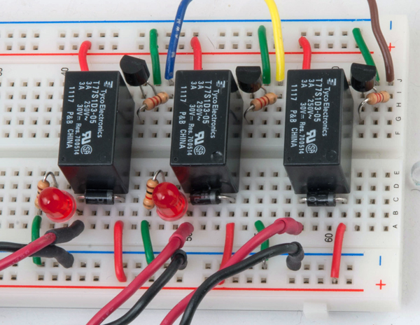
Electrolytic Capacitor in Solenoid Circuit
I was looking at a few solenoid circuits. I came across this one that had an electrolytic capacitor across it (whereas most just seemed to skip it).

-
Does this capacitor serve any other purpose than to create a smooth voltage particularly in regards to the flyback diode and transistor?
-
How can the appropriate capacitance be chosen? (More specifically for a 12-volt solenoid being powered from a LiPo or portable generator)
A capacitor like that is typically used to provide power for short-term current spikes in the circuit is is directly connected to.
A typical application that needs these type of capacitors (called bypass or filter capacitors) are digital integrated circuits that need a extremely short spike of power every time the state change, but are very low power as long as the state is steady. This spike is caused by internal parasitic capacitances that need to get quickly charged to a different voltage. The inductance of the connection to the power supply might be too high for the power supply to deliver the required current spike, so a capacitor is connected close to the circuit causing the spikes, so that the connection to it has less inductance.
Another use of capacitor for DC is a filter capacitor after an rectifier, to have voltage available even when the AC input is just crossing zero. In that case, I would consider the capacitor part of the power supply, not of the supplied circuit.
In your application, the load is dominated by the coil of the solenoid, which can be modelled as a series circuit of an inductor and a resistor. At turn-on time of the transistor, the inductive behaviour of the coil is dominant, causing a slow rise of the current, and afterwards the pure DC resistance of the coil determines the current, which needs to be constantly supplied while the solenoid is turned on. Neither during turn-on nor in the steady state, a short current spike is consumed, so the capacitor is pointless. Also your LiPo battery does not need a capacitor to deal with zero crossings, as it is a DC source.
Side note: A different situation occurs on AC solenoids with a significant movement of the core: The inductance of an AC solenoid with the core pulled in is significantly higher than at turn-on time. As AC current is determined by the impedance, which might be dominated by the inductance of the solenoid coil, the AC current during pulling can be many times higher than the current in steady active state, up to the destruction of an AC solenoid (due to continuous over-current) if the mechanical movement does not occur, because it is blocked. Of course, an electrolytic cap can not be used to catch the current spike of an AC circuit.
The purpose of the capacitor may be to provide current for the solenoid even if the power supply cannot do the job, for example if a battery is discharged such that he internal resistance is too high.
If you know that the solenoid current is i, the time the solenoid needs to operate is t, and the allowable voltage drop during the pulse is v, then the required capacitance C is:
C =
For example if the current is 400mA, the time is 0.2 second, and the allowable drop is 1.5V the required capacitance is 0.053F, or 53,000uF. This will give you an idea of the purpose of the capacitor. For a 3.7V battery you might use a somewhat higher standard value such as 63,000uF/6.3V.
COMBINE AND COMPARE ASCO NUMATICS SOLENOID VALVES FOR FUEL, GAS AND OIL SHUT OFF WITH ELECTRONICS SOLENOID VALVE
It is crucial before selecting a solenoid valve for fuel, gas and oil shutoff to understand the basics. If you would like to know more information about solenoid valves in general, read article “Solenoid Valves…The basics” before reading on.
The solenoid valves described below are valves ASCO Numatics have identified as being suitable for Fuel, Oil and Gas applications.
 Modular Gas Shut Off Solenoid Valves
- The 2/2 normally closed modular valve allows the combination of the 8214(200) solenoid valve with the V710(B) & AH(E) electro-hydraulic motorized valve
- Compact double valve design
- Ideal for the following appliances used in commercial and industrial applications
- Boilers
- Furnaces
- Ovens
- Kilns
- Heating equipment
- Gas generators
- Optional NPT threaded flange adapters are available for ease of installation and serviceability.
- Leading agency approvals
- Available in pipe connections from 3/4’’ to 3’’
Motorised Valves
- Designed for use in combustion systems
- Motorised valves are available in: 2/2 normally closed, 3/2 diversion
Features of motorised valves include:
- Pipe taps
- Visual indication
- Proof of closure
- Leading agency approvals
- Pipe connections from 3/4” to 6”.
Motorised valves are available in:
- Bronze
- Aluminium
- Cast iron
Motorised valves are rated for -40ºF service for outdoor installation in frigid climates.
 ASCO Numatics produce a broad line of solenoid valves & motorized shutoff valves. The solenoid valves ASCO Numatic offer in gas and oil applications are designed to control the flow of fuel gas, liquid propane, and all other grades of fuel oil used in combustion applications such as:
- Industrial furnaces
- Ovens
- Kilns
- Incinerators
- Burners
- Boilers
Asco Solenoid Valves and their uses:
- Direct-Acting Solenoid Valves. Direct-acting solenoid valves open the orifice of a normally closed valve or close the orifice of a normally open valve when the solenoid is energised. When de-energised, a spring returns the valve to its original position. Direct-acting solenoid valves will operate at pressures from 0 psi to its rated maximum. These solenoid valves are suitable for pilot and main fuel lines.
- Internal Pilot-Operated Solenoid Valves. Internal pilot-operated solenoid valves normally have a pilot and bleed orifice, which enables them to use line pressure for operation. When the solenoid is de-energised, the pilot orifice is closed and full line pressure is applied to the top of the piston or diaphragm through the bleed orifice, providing the seating force for tight closure. When the solenoid is energised, the core opens the pilot orifice, relieving pressure from the top of the piston or diaphragm via the outlet side of the valve. The line pressure then opens the valve by lifting the diaphragm or piston off the main orifice. Internal pilot-operated valves generally are used as main shutoff valves.
- Electrohydraulic Linear-Actuated Solenoid Valves. These solenoid valves provide users with slow-opening and quick-closing operation. When energised with line voltage, the electrohydraulic actuator pumps oil from one side of a piston to another to drive the actuator stem against the valve stem and sealing member to open the valve. When line voltage is removed from the actuator, return springs in both the actuator and valve body cause the actuator piston or stem to return to its de-energised position and cause the valve stem and sealing member to return to its closed position. These solenoid valves are important for controlling the flow of fuel to the burner upon initial system startup.
Choosing the correct Solenoid Valve for your Fuel, Oil or Gas application:
It is important to clearly define specific parameters of your application for appropriate valve selection. These parameters include:
- Fuel type (gas or oil)
- Fuel viscosity (if oil)
- Ambient and fluid temperature range
- Pipe size
- Flow requirement
- Oerating pressure range
- Voltage (AC or DC)
- Required approvals (UL, FM, CSA, etc.)
- Visual or electrical
- Visual position indication
Importance in considering the media in order to find the appropriate solenoid valve for the application
For fuel gas service, generally a brass, aluminum, cast iron or steel bodied valve with nitrile rubber sealing is an appropriate choice for maximum life and performance
Natural Gas
- Compatible with aluminum, brass, cast iron or steel body materials and nitrile rubber for the valve seal material.
- Can be applied from very low pressure (inches w.c.) through to high pressure (30 psi or greater)
- Gas pressure often is used to reduce the line size of the fuel line and related components
- If your application will see ambient temperature extremes, be sure the valve is rated accordingly
- Low ambient temperatures such as -40oF (-40oC) require special low temperature elastomers for leak-tight sealing.
- High ambient temperatures may require Class H coil insulation to ensure reliable operation
Fuel Oil
- In a fuel oil system, you must consider fluid temperature (as viscosity changes with temperature), pressure and the GPM that you require
- A brass-bodied valve with Viton sealing is generally an appropriate choice for maximum life and performance
- The Viton elastomers provide a balance of material compatibility and long life
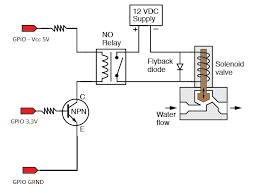
Advancements in Technology
Over the years basic solenoid valve application and design has hardly changed. However significant advancements have been made in terms of power management. Electronic technology has been integrated into new solenoid valve designs to decrease power consumption from typically 10 W to 2 W. Additional features derived from use of electronic circuits include lower temperature rise resulting in extended life of electrical components, DC operation at AC pressure, and flow ratings as well as built-in surge suppression for coil protection.
Solenoid valves and electrohydraulic-operated fuel shutoff valves have a substantial history and a bright future for individuals who define their fuel shutoff valve application requirements.
Structure diagram of the IL-IE device: 1: pump, 2: solenoid valve, 3: flow sensor, 4: pressure sensor, 5: ventilator connecting port, and 6: pneumatically operated membrane valve.

How do I work out the transistor needed?
need help with determining the transistor needed to power about 17 solenoid valves with a Raspberry Pi which produces 3.3V. I have made this diagram with the circuit:
(There will be 17 connections to GPIO pins on the Raspberry Pi, 17 transistors and 17 solenoids)
I need to know how to work out the transistor needed. Also, will any 12v power supply suffice? And do I need a resistor in this circuit?
Explain the circuit (transistor, relay, transistor, interface )
explain the circuit (transistor, relay, transistor, interface to Arduino, power supply)

WORKING The above circuit is used to control the valve action i.e opening and closing of devices like ballasts using an inductive coil or solenoid. It uses two diodes, one connected between ground terminal and emitter terminal of the npn-BJT .
XXX . XXX 4%zero null 0 1 2 3 4 Solenoid Valve Control example in piano concept
The easiest way to use a Wintel computer to control striking mechanical objects (keys, bars, drums, cymbals, valves...) consists of using one a more I/O adresses , bringing these ports out after latching the data contents, and use the signals directly to drive bases or gates of power darlingtons or Mosfets which can switch the required solenoids on or off. If you want it to be midi controlled, Pavo offers a relatively cheap solution in the form of their midi computer kit with 64/128 output driver device. No way to use the midi velocity however along this track...
If the solenoids are powered from a supply with a voltage of ca. 2 to 5 times the nominal operating voltage of the coils, it becomes possible to controll the impact of the strokes through software: by carefully controlling the time (the width) of the pulse applied to the solenoid. Of course you have to guarantee that no coil ever stays under tension, since they are guaranteed to burn out under these circumstances. If the instrument required the anchors to stay in touch with the object, it is enough to apply a constant voltage, just a bit over the minimum holding voltage, to all solenoids.
Pulsewidth modulation offers another alternative possibility. But, when attempting to handle this through software only, you may quickly run into serious problems, particularly if the instruments you wanted to build, had to be polyphonic... Also, the solenoids when driven by PWM signals tend to get rather noisy...
Since in all struck instruments (pianos included) the volume is only dependent on the impact of the solenoid anchor on the object, it is enough to controll the energy supplied to the coils during the attack period.
Hardware approach:
In instruments such as the player piano, we had to derive this information from the velocity bytes in the note-on midi command, for each note individually. The data analysis of the midi stream was left to a dedicated microprocessor system. The controll however, still involves some electronic circuit bending. One of the very first working ideas we developped looked like this:
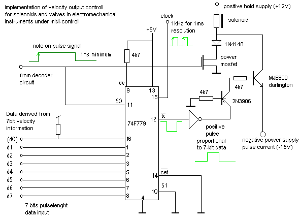 Note that this circuit has to be build once for every single object your instrument has to strike. So parts count will build up with the number of keys. This anyhow, if you want your instrument to have fast response and complete and true polyphonic possibilities.
The circuit around the 74F779 or 74HCT779 chip (a synchronous TTL counter) behaves as a digitally controllable monostable oscillator (a monoflop). A rising edge on the note on signal starts the counter and as long as pin 11 stays 0, new values appearing on the 7bit data input, are load into the count register. Counter data is latched into the register as soon an the signal on pin 11 goes high, so an external latch is not required. The counter is operated in count-down mode, starting from the value load on its input register. As soon as count 0 is reached, the TC (terminal count) output (pin 12) goes high. Hence also, the inverter following pin 12 of the 74779. The software has to guarantee that the note and velocity bytes are inverted in time, as compared to the order used in the midi protocol. First the velocity byte has to be send, only than the notebyte to which this information applies. Since the chip is synchronous, the user has to guarantee a clock pulse between the velocity data and the note-on command pulse. This could be realized through hardware as well, but we did'nt want to obscure the schematic too much. If you want to further develop this idea: it's quite simple, just insert a monoflop, triggered on the rising edge of the note hold signal. As to the counter used, a 74579 chip could be used as well, but pinning is different. The 74F579 comes in a 20 pin DIL package and has multiplexed I/O registers. The 74F269 can also be used, but occupies a large board space with its 24 pins and separate input and output ports. As I heard from some students, nowadays (2001) there seems to be increasing problems in getting these TTL components. So, before you start building this circuit, make sure you can get the required chips.
Note that the dynamic range can be tightly adjusted -controlled if you want, even by midi continuous controller commands- by adjusting the clock frequency. Exact settings depend highly on the types of solenoids used.
A similar approach is also possible using analog timer chips such as the infamous 555. In this case the velocity information should be converted to analog (an R2R network does just fine here) voltage fed into the control voltage input of the 555.
If you want optimum resolution , up to 16 bits (which is a lot better than even Boesendorf's player piano, using only 12 bit resolution...) , and highly flexible design, you could also opt for the classic 8253/8254 Intel timer chips. These chips contain 3 independent software programmable timers and can be easily configured for one-shot operation such as required for our purpose here. For a full 127 note controller you will need no less than 43 of these chips. If you have a choice, it will be almost mandatory to go for the C-Mos version (82C84).
A suitable circuit schematic for a board covering 12 notes or a full octave looks like this:
Note that this circuit has to be build once for every single object your instrument has to strike. So parts count will build up with the number of keys. This anyhow, if you want your instrument to have fast response and complete and true polyphonic possibilities.
The circuit around the 74F779 or 74HCT779 chip (a synchronous TTL counter) behaves as a digitally controllable monostable oscillator (a monoflop). A rising edge on the note on signal starts the counter and as long as pin 11 stays 0, new values appearing on the 7bit data input, are load into the count register. Counter data is latched into the register as soon an the signal on pin 11 goes high, so an external latch is not required. The counter is operated in count-down mode, starting from the value load on its input register. As soon as count 0 is reached, the TC (terminal count) output (pin 12) goes high. Hence also, the inverter following pin 12 of the 74779. The software has to guarantee that the note and velocity bytes are inverted in time, as compared to the order used in the midi protocol. First the velocity byte has to be send, only than the notebyte to which this information applies. Since the chip is synchronous, the user has to guarantee a clock pulse between the velocity data and the note-on command pulse. This could be realized through hardware as well, but we did'nt want to obscure the schematic too much. If you want to further develop this idea: it's quite simple, just insert a monoflop, triggered on the rising edge of the note hold signal. As to the counter used, a 74579 chip could be used as well, but pinning is different. The 74F579 comes in a 20 pin DIL package and has multiplexed I/O registers. The 74F269 can also be used, but occupies a large board space with its 24 pins and separate input and output ports. As I heard from some students, nowadays (2001) there seems to be increasing problems in getting these TTL components. So, before you start building this circuit, make sure you can get the required chips.
Note that the dynamic range can be tightly adjusted -controlled if you want, even by midi continuous controller commands- by adjusting the clock frequency. Exact settings depend highly on the types of solenoids used.
A similar approach is also possible using analog timer chips such as the infamous 555. In this case the velocity information should be converted to analog (an R2R network does just fine here) voltage fed into the control voltage input of the 555.
If you want optimum resolution , up to 16 bits (which is a lot better than even Boesendorf's player piano, using only 12 bit resolution...) , and highly flexible design, you could also opt for the classic 8253/8254 Intel timer chips. These chips contain 3 independent software programmable timers and can be easily configured for one-shot operation such as required for our purpose here. For a full 127 note controller you will need no less than 43 of these chips. If you have a choice, it will be almost mandatory to go for the C-Mos version (82C84).
A suitable circuit schematic for a board covering 12 notes or a full octave looks like this:
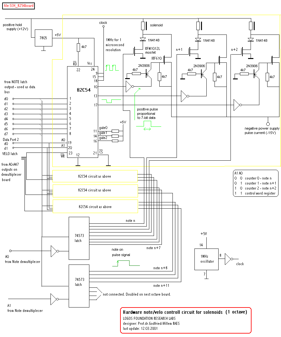 Circuit boards for this design are available from the author. Each board can accomodate all required components for a full octave (12 notes). The chip and semiconductor component list is:
- 4 82C54 timer chips
- 2 74HCT14 schmitt trigger/buffer
- 1 1MHz integrated oscillator ( for 1 microsecond resolution)
- 3 74HCT10 tripple nand gates
- 12 power mosfets RFM1020L
- 12 power mosfets IRF610
- 12 1N4007 diodes
- 12 BYV27 diodes
- 12 transistors (PNP) 2N3906 or similar
- 2 Latches 74HCT573
The PC board for this circuit is depicted below:
 We also designed PC boards covering two octaves. The problem with this design though, is that you need a A3 size printer to print the transparants for making the films. However, with this design you need only 4 boards for a piano and the wiring is greatly simplified. Here is the board:
 The above board works best together with the specially designed demultiplexer board, working with a National Instruments DIO PCMCIA card. (see further)
Of course, the required software, although straightforward, ought to be worked out as well. Reading Intel's data sheet on the timer chip is essential. Support from within <GMT> is provided by the author, to simplify designs and further research. The schematic for a suitable demultiplexer to connect to your printer port is:
 A suitable PC board (real size,but the gif file is 200% however) ) for the above multiplexer circuit used to steer these circuits from your printerport (or any other parallel port) looks like:
 Note that using the printer port is impossible on NT machines or Windows 2000. To use the design on those operating systems, we use a National Instruments DIO PCMCIA card (PCI cards that are completely compatible are available as well). Since 2002, we have also implemented USB ports to work with our hardware. The schematic for the NiDAQ design is:
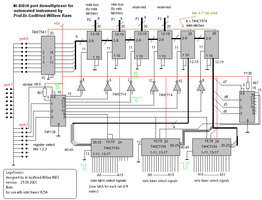 Of course, we also designed a printed circuit boards for this schematic. It works best in combination with the 2-octave boards shown above.
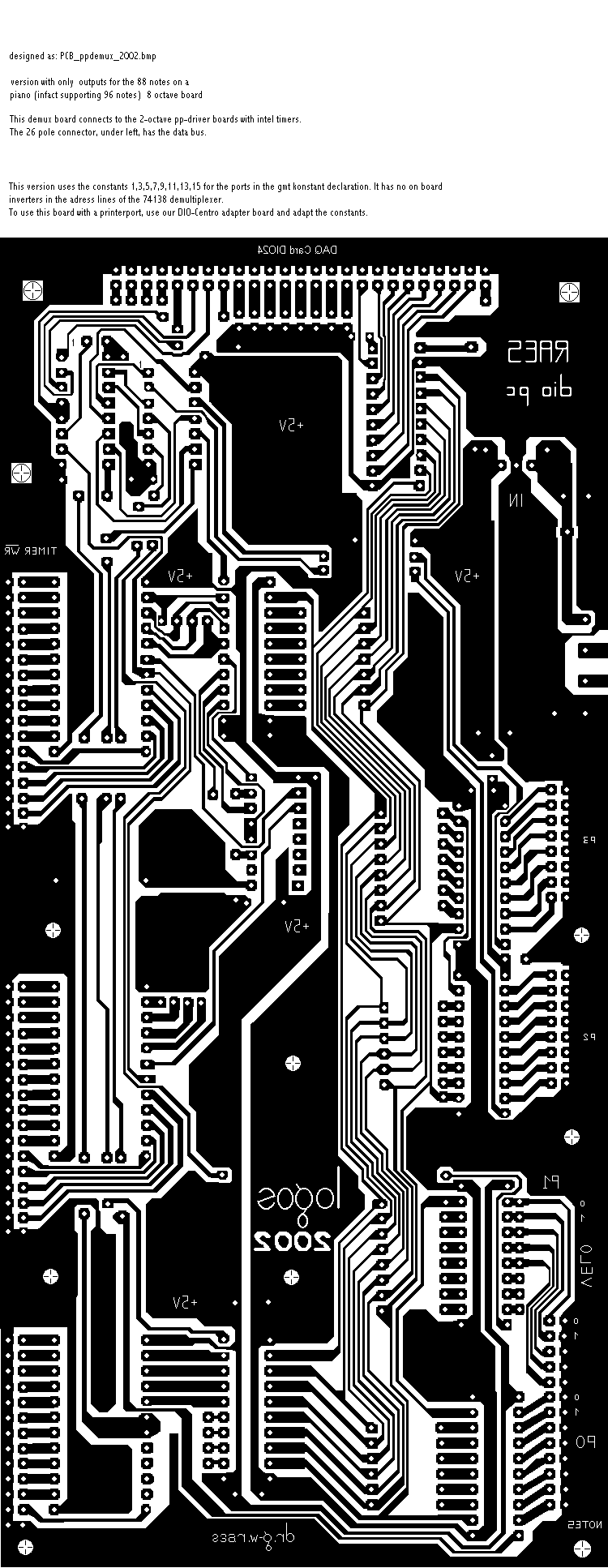 To give an idea about how to write code for this design, we give here a small excerpt from our <GMT> project:
Constant definitions:
To give an idea about how to write code for this design, we give here a small excerpt from our <GMT> project:
Constant definitions:
- %Padr = adres of your printer port, or any other (centronics compatible) port you might connect the hardware to (mostly &H378)
- %Preg = %Padr + 2
- %CtrlHiNib = 80 ' bin 0101 0000
- %NoteReg = %CtrlHiNib + 0 ' bin 0101 0000
- %VeloReg = %CtrlHiNib + 2 ' bin 0101 0010
- %Ext1Reg = %CtrlHiNib + 4 ' bin 0101 0100
- %Ext2Reg = %CtrlHiNib + 6 ' bin 0101 0110
- %SelNotePort = %CtrlHiNib + 8 ' bin 0101 1000 sets 4 bit adres for 74154, selecting the note latch
- %SelVeloPort = %CtrlHiNib + 10 ' bin 0101 1010 sets 4 bit adres for 74154, selecting the velo latch ' on the 82C54 board we use 6 bits.
- %NoteOut = %CtrlHiNib + 12 ' bin 0101 1100 causes 74154's to output a strobe pulse latching notebits
- %VeloOut = %CtrlHiNib + 14 ' bin 0101 1110 causes 74154's to output a strobe pulse latching velobits
Procedure for note ON:
SUB g_Note (BYVAL note AS BYTE, BYVAL velo AS BYTE) EXPORT
LOCAL retval AS LONG
LOCAL wvelo AS WORD ' 16 bit value
LOCAL cw AS BYTE
LOCAL param AS BYTE
IF ISFALSE velo THEN
       ppHold note, %False
       EXIT SUB
ELSE
       ppHold note, %True
END IF
wvelo = velo * 512 ' linear mapping, for test only - range 0.2ms to 65ms
PortOut %Preg,%VeloReg
PortOut %Padr, &B11 ' A0=1, A1=1 implies command writing to 82C54
Strobe %Preg,%Veloreg,0,%StrobeLength
PortOut %Preg,%NoteReg
cw = note MOD 3
SHIFT LEFT cw,6
BIT SET cw,5
BIT SET cw,4 ' 16 bit loading - lsb first! M0, M1, M2 = 0 for mode 0 counting, BCD= 0 for 16 bit binary counting, in microsecond units
PortOut %Padr, cw
Strobe %Preg,%NoteReg,0,%Strobelength
param = note \ 3
PortOut %Preg,%SelVeloPort
PortOut %Padr, param
Strobe %Preg,%SelVeloPort,0,%StrobeLength ' now we generate a strobe such that the 74154 selects the correct timer and latches the data
PortOut %Preg, %VeloOut ' send a strobe pulse
Strobe %Preg,%VeloOut,0,%StrobeLength ' now we should send 2 bytes of timer data (the velo information in 16 bits):
PortOut %Preg,%NoteReg
PortOut %Padr, LOBYT (wvelo)
Strobe %Preg,%NoteReg,0,%StrobeLength ' set A0,A1 to the correct timer:
Portout %Preg,%VeloReg ' we use this port to select the timer adresses via  A0,A1 = D0,D1
PortOut %Padr, note MOD 3 ' 0 = timer 0, 1=timer 2, 2= timer 3, 3= controll
Strobe %Preg,%VeloReg,0,%StrobeLength ' generate a strobe to latch this byte into the timer
Strobe %Preg,%SelVeloPort,0,%StrobeLength ' now once again for the MSB of the velo data:
PortOut %Preg,%NoteReg
PortOut %Padr, HIBYT (wvelo)
Strobe %Preg,%NoteReg,0,%StrobeLength
Strobe %Preg,%SelVeloPort,0,%StrobeLength ' now both lsb and msb have been sent to the timer. It should now be counting...
END SUB
For complete code examples in the context of a working program, look into out <GMT> source code. The appropriate procedures reside in the code module g_nih.dll or g_noh.dll. (Source code is in the module g_h.bas)
Of course criticism is possible on the rather large size of such a project. Unfortunately we could not retrieve information as to timer chips that would contain more than 3 timers... It's very hard to believe that the industry would not have a good use for timerchips containing at least 16, and why not 256..., independent timers... A similar remark is valid for the non availability of DAC chips with built-in sample and hold and more then 16 output channels...
An assembled board covering a single octave looks like:
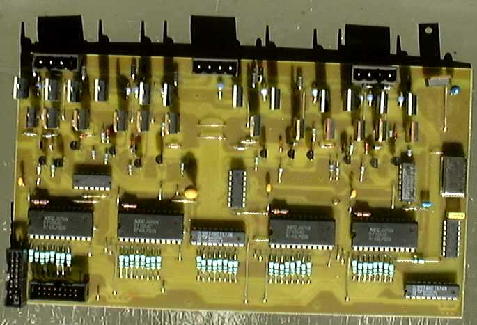 These board can be purchased from the Logos Laboratories. Delivery time is ca. 4 weeks. Fully assembled, a board costs 350Euros (price as of 22.09.2001). Two octave boards are around 500 Euro. Enquire by .email
Solenoid hardware
For player pianos and similar keyboard instruments we advise the use of STA Series push tubular solenoids manufactured by Lucas Ledex in Vandalia, Ohio. The type number to order is 195207-2-28, for solenoids with following specs:
- - Coil resistance (at 20 Celsius): 19.2 Ohms
- - Allowable voltage at 100% duty cycle: 13.8V (unlimited ON-time) Power: 10W
- - Allowable voltage at 50% duty cycle: 19.6V (ON-time < 360s, in single pulse: < 470s). Power: 20W
- - Allowable voltage at 25% duty cycle: 28V (ON-time < 32s, in single pulse: < 120s). Power: 40W
- - Allowable voltage at 10% duty cycle: 44V (ON-time < 8s, in single pulse: < 32s): Power: 100W
Simplistic approach:
In theory everyone should be capable of designing electromechanical and midi controlled instruments, using one of the nice kits Pavo sells. They should have a kit with a possibility to write the programm in the PROM yourself on a Wintel PC... at least that's what their add claims.
As to the kit for controlling up to 128 solenoids/relays from their catalogue, we have tried it and warn potential buyers for some inherent limitations of the design:
- NO velocity controll provided.
- The manual pretends each output to be capable of sinking 500mA. This is absolutely incorrect, since the darlington driver chips used have only a power handling rating (absolute maximum!) of 1.5Watts, for all 8 drivers together. In practice you should limit the current to about 65mA for each output if you anticipate real polyphonic use. We modified the boards , by adding no less than 128 power mosfets to switch our 24V / 40 Ohm solenoid valves. The IRF540 mosfet handles this very nicely. Pavo should redesign their boards to allow users to do this modification easily and cleanly. However, Pavo board can be used in connection with our own mosfet driver boards , as will be explained further.
- The numbering scheme of the connectors is a bit awkward. There is no instruction in the manual as to how to freely reprogram the mapping table to make this more handy.
Multitasking approach:
An alternative to the hardware approach above, consists of using a multitasker to controll the individual solenoids. Here you have to set up a single task for each solenoid (so 88 for a player piano..., 128 tasks if you want a universal controller accepting all midi notes, or many more if you want to dig into the world of microtonal automated instruments...). Our <GMT> software (version > 4.18) can handle all this perfectly well. If you are not yet familiar with GMT, we refer you to chapter 1 of this course as well as to the relevant manuals on our website: http://www.logosfoundation.org/logos/gmt/gmt_intro.html
Each single key-task then controlls the ON time for the velocity pulse as well as the hold-pulse. The hardware becomes much simpler now and it is possible to just use the printer output port from a normal PC. You have to buffer the input. The schematic can be represented in block diagram as:
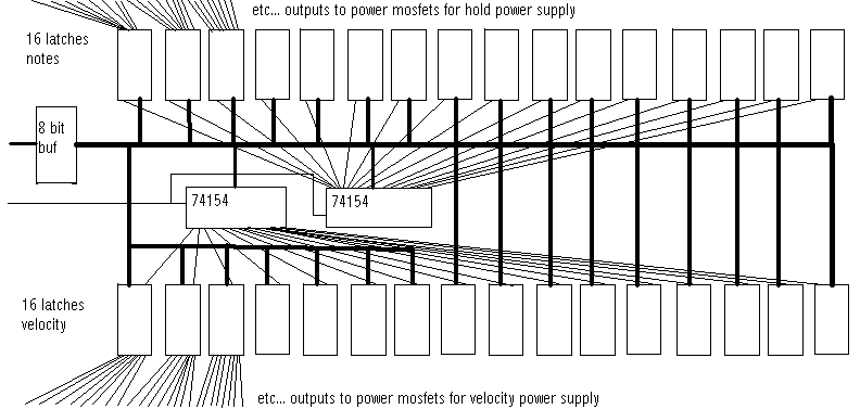 The above circuit sketch allows for up to 128 notes with 128 individual velocity controlls. The velocity controll can in this approach have virtually unlimited resolution. Of course you can save on chip count, by leaving out notes your application does not require. In any case you need two 8-bit latches for each group of 8 solenoids (and notes).
DETAILS:
A detailed -and tested- schematic for a demultiplexer boards looks like: (this circuit fits easily on a single Eurocard):
The above circuit sketch allows for up to 128 notes with 128 individual velocity controlls. The velocity controll can in this approach have virtually unlimited resolution. Of course you can save on chip count, by leaving out notes your application does not require. In any case you need two 8-bit latches for each group of 8 solenoids (and notes).
DETAILS:
A detailed -and tested- schematic for a demultiplexer boards looks like: (this circuit fits easily on a single Eurocard):
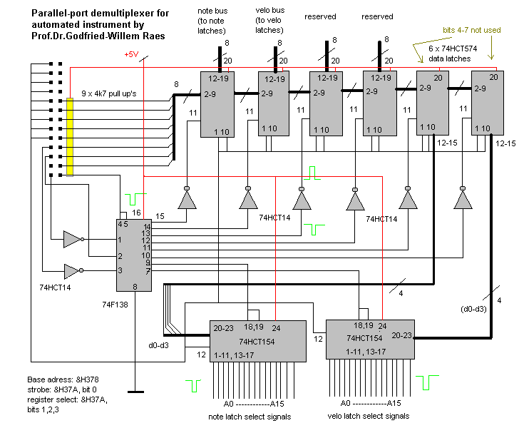 This board (just as the 8254 boards described before) can also be used with National Instruments DIO boards, if you use our adapter board to convert this output into something simular to standard printer ports. One of the reasons for going into NiDAQ devices having to with the fact that under Windows NT and Windows 2000 it is no longer possible to directly adres and use the ports of your PC. (Blame Bill Gates for this theft of property!). Software for both standard printer ports and NiDAQ devices is included in our GMT project.
Once you got this up and working, you can start building the note/velocity decoder boards. You need 1 board for each set of 2 octaves. So if we start from midi note 0,
the mapping is:
This board (just as the 8254 boards described before) can also be used with National Instruments DIO boards, if you use our adapter board to convert this output into something simular to standard printer ports. One of the reasons for going into NiDAQ devices having to with the fact that under Windows NT and Windows 2000 it is no longer possible to directly adres and use the ports of your PC. (Blame Bill Gates for this theft of property!). Software for both standard printer ports and NiDAQ devices is included in our GMT project.
Once you got this up and working, you can start building the note/velocity decoder boards. You need 1 board for each set of 2 octaves. So if we start from midi note 0,
the mapping is:
- board 1 : notes 0 -23
- board 2: notes 24-47
- board 3: notes 48 - 71
- board 4: notes 72 - 95
- board 5: notes 96- 119
- board 6: notes 120-127 (this board handles only 8 notes, and in most cases will not be needed.)
The circuit looks like:
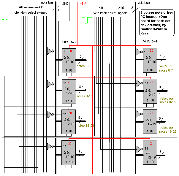 So each board houses 6 74HCT574 latches. The inverters are 74HCT14, or anything similar. The outputs for the latches go to darlington and mosfet drivers as shown in our first schematic above. It is very well possible (and favorable for heat losses...) to substitute another power mosfet for the darlington, as shown in the schematic below:
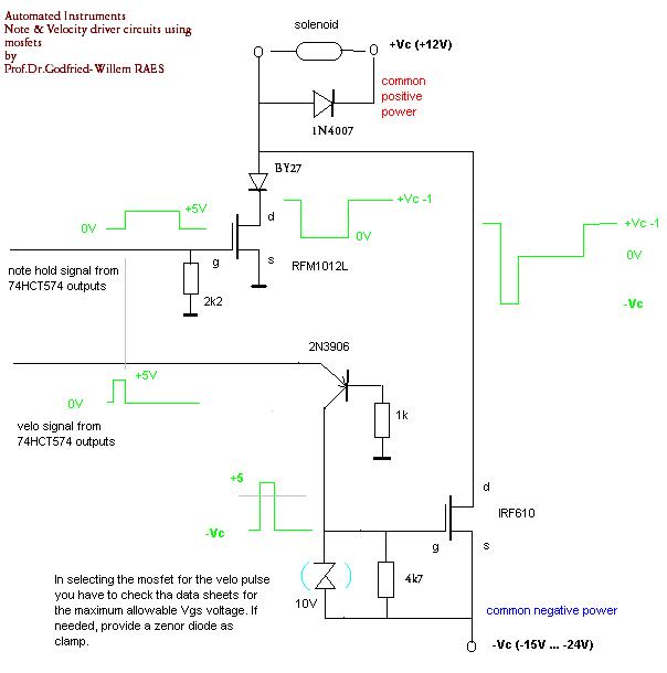 With components -and voltages- shown, you can use any type of coil in as far as the current drawn does not exceed 2.5Amps, since that is the limit for the power mosfets. The coils we use are rated for continuous operation at 12 Volt. So, under no circumstances should you leave on the velocity voltage. In normal circumstances you do not need cooling for the mosfets. For the 2N3906 almost any fast small signal PNP transistor can be substituted. (Such as BC307, BC512, BC557, BC251, BC212, 2N3905...). The 2N3906 is rated at 40V / 200mA Ic. Power rating 0.35W, beta=100.
If you shop for mosfets, for the note-hold mosfet, make sure you use types that fully fire with gate voltages below 5Volts! The 4k7 resistors are not always required. They serve as protection for the mosfets in case the board gets disconnected and help discharging the gates faster during operation, thus limiting dissipation.
Possible alternatives for the note-hold mosfets are:
With components -and voltages- shown, you can use any type of coil in as far as the current drawn does not exceed 2.5Amps, since that is the limit for the power mosfets. The coils we use are rated for continuous operation at 12 Volt. So, under no circumstances should you leave on the velocity voltage. In normal circumstances you do not need cooling for the mosfets. For the 2N3906 almost any fast small signal PNP transistor can be substituted. (Such as BC307, BC512, BC557, BC251, BC212, 2N3905...). The 2N3906 is rated at 40V / 200mA Ic. Power rating 0.35W, beta=100.
If you shop for mosfets, for the note-hold mosfet, make sure you use types that fully fire with gate voltages below 5Volts! The 4k7 resistors are not always required. They serve as protection for the mosfets in case the board gets disconnected and help discharging the gates faster during operation, thus limiting dissipation.
Possible alternatives for the note-hold mosfets are:
- RFP10N12 (Harris Semiconductor), rated for 10Amps at 120V. (Gate-Source capacity is 850pF!!!). This fires with less then 4Volts. [equivalent nomination for this type is IRL640]
- RFP2N12 , rated for 2Amps at 120V (200pF).
- RFL2N05, rated for 2Amps at 50V
- RFP4N06L, rated for 4Amps at 60Volt
As to the velo-pulse mosfets, the situation is slightly different. In the schematic as shown, the pulse on the collector of the PNP transistor, connected to the mosfet gate, ranges from -Vcc to +5V. If you do not fit a zener diode, you have to select a power mosfet capable of withstanding a Vg of this amplitude. The IRF540, 610 etc. series can withstand 20V on their gates, so if you use this type, -Vc should not exceed -15V. If you consider using the RFP... types, notes that without extra protection, the -Vc voltage should not be larger than -5V. It will be clear that this would compromise the controll range for the velocity pulses. By fitting a zener diode between the gate and -Vc of the mosfet, you can limit the gate voltage to a safe value for the mosfet you select.
For all our applications we have never used cooling on the Mosfets. You can calculate dissipation easily as follows:
- - look up Ron for the gate voltage Vg used (the smaller Ron, the better...)
- - measure Rdc for the solenoids used (note that this value rises when the coils get hot...)
- - On-current through coil and mosfet equals: I = +Vc / (Ron + Rdc) (note hold mosfets) or I = +Vc + ABS(-Vc) / (Ron + Rdc) (velo pulse mosfets)
- - Voltage drop over the mosfet Vf= I * Ron
- - Power dissipated in the mosfet P = Vf * I
You should try to limit this value to below 2Watts.
Since the switching speeds in this application are very low, we can safely neglect the dissipation caused by charging/discharging the gates.
Under no circumstances should you forget the surge protecting diodes over the solenoids. Any reasonably fast 1Amp 200V diode will do. Note that you need as many driver circuits as you have notes on the instrument you want to automate.
The software was implemented under <GMT>, and is available (if not found on this website) on request. Note that since this player piano inherently does not use midi (although the software allows users to just control the piano (or other automated instrument) via midi command), we are not limited to the slow speed so typical for midi! So, here -provided our power supply is powerfull enough-, we can indeed play 88-note clusters. without making them sound as arpeggios.
To make the software a mirror of the hardware implementation, we created a specific prototype for our code, wherein each element contains the exact bit contents of each latch:
TYPE Akeys BYTE ' makes a single 128-bit variable, if adressed by its pointer.
b000007 AS BYTE ' contents of latch 1
b008015 AS BYTE ' contents of latch 2
b016023 AS BYTE ' contents of latch 3
b024031 AS BYTE ' contents of latch 4
b032039 AS BYTE ' contents of latch 5
b040047 AS BYTE ' contents of latch 6
b048055 AS BYTE ' contents of latch 7
b056063 AS BYTE ' contents of latch 8
b064071 AS BYTE ' contents of latch 9
b072079 AS BYTE ' contents of latch 10
b080087 AS BYTE ' contents of latch 11
b088095 AS BYTE ' contents of latch 12
b096103 AS BYTE ' contents of latch 13
b104111 AS BYTE ' contents of latch 14
b112119 AS BYTE ' contents of latch 15
b120127 AS BYTE ' contents of latch 16
END TYPE
In the code we use two global variables Vkey and Nkey, standing for the contents of the velocity latches and note-latches respectively.
There are different approaches possible. First we can define individual tasks within GMT, one for each key:
1.- Individual key-task implementation:
The task-code written in PowerBasic - we give here the code snippet for midi-keys 0 and 1- to run in <GMT> looks like:
- SUB Toets0()
' bit 0 of lowest data-latch
' the note to play does not have to be passed, as each note gets a task of its own.
' the velocity is passed in Task().level
LOCAL note AS BYTE
note = 0
IF ISFALSE Task(%Toets0 + note).level THEN
' switch note off, if it was ON
IF BIT (Vkey.b000007,note) THEN ppVelo note, %False
IF BIT (Nkey.b000007,note) THEN ppHold note, %False
StopTask %Toets0 + note ' this also resets Task().tog- EXIT SUB
END IF
IF ISFALSE Task(%Toets0+ note).tog THEN
ppVelo note, %True' reschedule the task...
ReScheduleTask %Toets0 + note, Coeff(Task(%Toets0+ note).level) ' freq. is declared as single precision
Task(%Toets0+ note).tog = %True
EXIT SUB
END IF
ppVelo note, %False ' velo bit off
ppHold note, %True ' hold ON
StopTask %Toets0 + note ' note stays on until task is switched on again, with level set to zero.
- END SUB
-
SUB Toets1()
LOCAL note AS BYTE
note = 1
IF ISFALSE Task(%Toets0+ note).level THEN
IF BIT (Vkey.b000007,note MOD 8) THEN ppVelo note, %False
IF BIT (Nkey.b000007,note MOD 8) THEN ppHold note, %False
StopTask %Toets0 + note
EXIT SUB
END IF
IF ISFALSE Task(%Toets0 + note).tog THEN
ppVelo note, %True
ReScheduleTask %Toets0 + note, Coeff(Task(%Toets0 + note).level)
Task(%Toets0 + note).tog = %True
EXIT SUB
END IF
ppVelo note, %False
ppHold note, %True
- END SUB
2.- In a second approach, we do not have to use tasks at all, but we take profit of the multimedia timers integrated in the Win32api. These timers are interrupt based. They make use of callback functions that we have integrated into our DLL library. However, in this approach we are limited to the timing resolution of the PC used and to the amount of simultaneous timers windows supports.
The code to make our player piano listen to midi-input (we have one such task for each midi channel, the channel can be selected by the user from the command cockpit in GMT) simply looks like:
- SUB ppListen0 ()
LOCAL nv AS INTEGER
LOCAL noot?
LOCAL velo?
nv = GetMidiNote% (Task(%ppListen).channel, %Remove OR %Oldest)
IF nv = %NotFalse THEN
EXIT SUB
- ELSE
velo? = LOBYT (nv)
noot? = HIBYT (nv)
- END IF
ppNote noot?, velo? ' this procedure resides in gmt_lib.dll
IF velo? THEN
AddNote2Har Task(%ppListen).Har, noot?, velo?
- ELSE
DelNote2Har Task(%ppListen).Har, noot?
- END IF
END SUB
To see the latest complete source, cfr: http://www.logosfoundation.org/logos/gmt/gmt_pp.inc . Note that the low level driver code resides in gmt_lib.dll, thus hiding musicians for error prone coding that could possibly damage the hardware.
Better even, download the complete GMT in zipped form: http://www.logosfoundation.org/logos/gmt/gmt_source.zip
If the interest in this building project is high enough, we consider offering PC-boards for all above circuitry. Contact the author by email: godfriedwillem.raes@logosfoundation.org
A design for the parallel port demultiplexer looks like this:
If you want to etch it, this artwork has to be placed in contact with the photosensitive layer of the PC board.
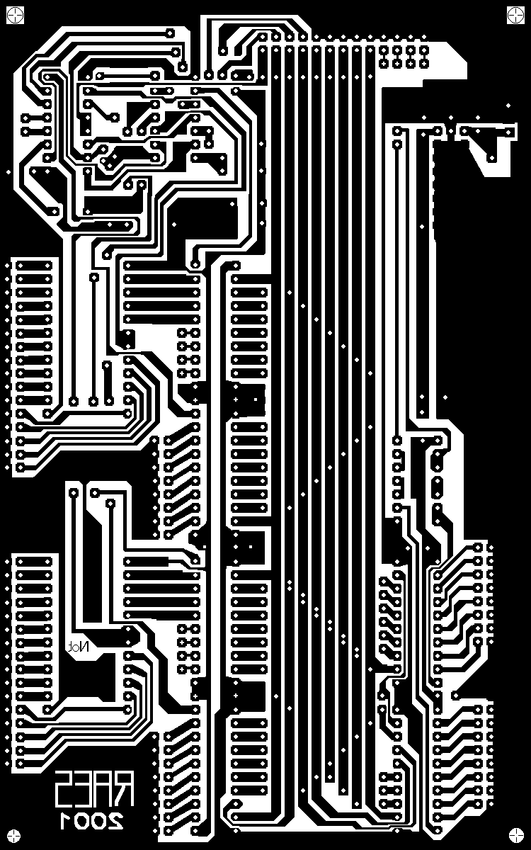 The PC-boards containing 2 octaves of note drivers may look like:
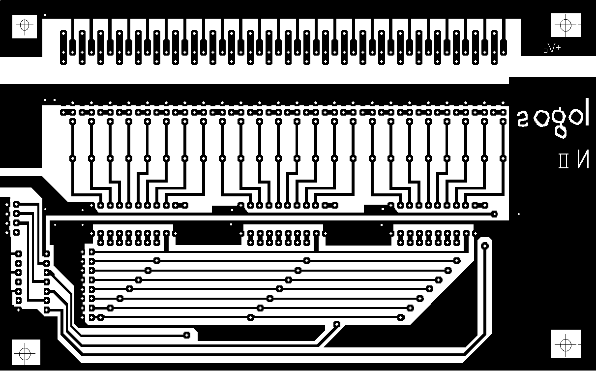 The last board you will need, is for the velocity drivers. Again , the following artwork is a single eurocard board covering 2 octaves:
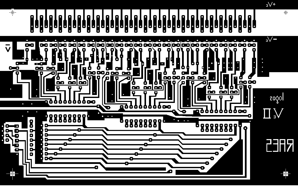 If you want to make your own PC boards, then you can print this artwork with a laser printer on tranparancies as used for overhead projectors. These films can be used to expose the photosensitive PC boards directly.
We made a quick picture of one of these note-hold boards:
If you want to make your own PC boards, then you can print this artwork with a laser printer on tranparancies as used for overhead projectors. These films can be used to expose the photosensitive PC boards directly.
We made a quick picture of one of these note-hold boards:
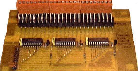
Notes:
1.- as off 01.02.2000: PC boards as well as complete kits for the above project are available from the author. Pricing information can be obtained by email: godfriedwillem.raes@logosfoundation.org
- Bare demultiplexer boards: tinned and drilled, on epoxy board: 40.00 Euro. With components, fully tested: 150.00 Euro
- Note driver boards: tinned and drilled, on epoxy board: 30.00 Euro. With components, fully tested: 120.00 Euro
- Velo driver boards: tinned and drilled, on epoxy board: 35.00 Euro. With components, fully tested: 150.00 Euro
Prices for note and velo board depend on the solenoids you want to use (current and voltage) as well as on whether you want darlingtons or mosfets.
We also designed compatible boards to controll heavy duty stepping motors, since we needed these in our automated rototom instrument. (cfr. Rotomoton).
2.- The note-hold boards described here can also be used with PAVO's midi kits. These kits do not support velocity information handling however. The advantage is only that no PC is required to controll your automated instrument.
The circuit we designed -to be connected to the DIL header labeled J5, expand conn. provided on PAVO's controller board, looks like:
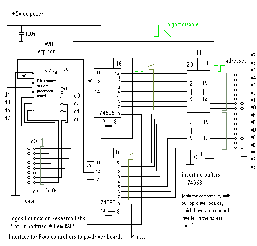 PC boards for this circuit are available also from the author. If you want to do the etching yourself, here is a suitable PC board layout:
++++++++++++++++++++++++++++++++++++++++++++++++++++++++++++++++++++
CONTROL AND INSTRUMENT SOLENOID VALVE COMBINE TRANSISTORS
++++++++++++++++++++++++++++++++++++++++++++++++++++++++++++++++++++
0
The power required to activate a high pressure water solenoid will need more than a transistor and 9V battery. I expect the solenoid value <10 Ohms and you need a 100 milliOhm MOSFET.
The 9V battery might be able to supply the base current only but not activate 1 or more solenoids of low DCR.
It is imperative to define load voltage current and make the switch <<5% resistance or so less than the DCR of the solenoid to avoid heat heat rise.
- Define specs before you design.
- Test your assumptions afterwards
- Verify specs.
- Use reverse clamp diode across solenoid to protect driver from Turn off high V.
- Use a low side switch Nch between solenoid and V+
Rotary Solenoid
Pushbutton Switch
Pushbutton Switch
DC Motor is an
Output Device
Output Device
V1=0 ===> Vout=9v
V1=3.3v ===> Vout=0v
Then I willl have to choose a transistor which is able to supply me 0.75A of minimum collector current. Am I right in this case?
One funny thing that I observed while sourcing for a solenoid actuator is a small actuator needs 12VDC to be operated, while the one I purchased which is bigger than the small one only need the range 6V - 12V. Is this got to do with the number of coils on the solenoid?
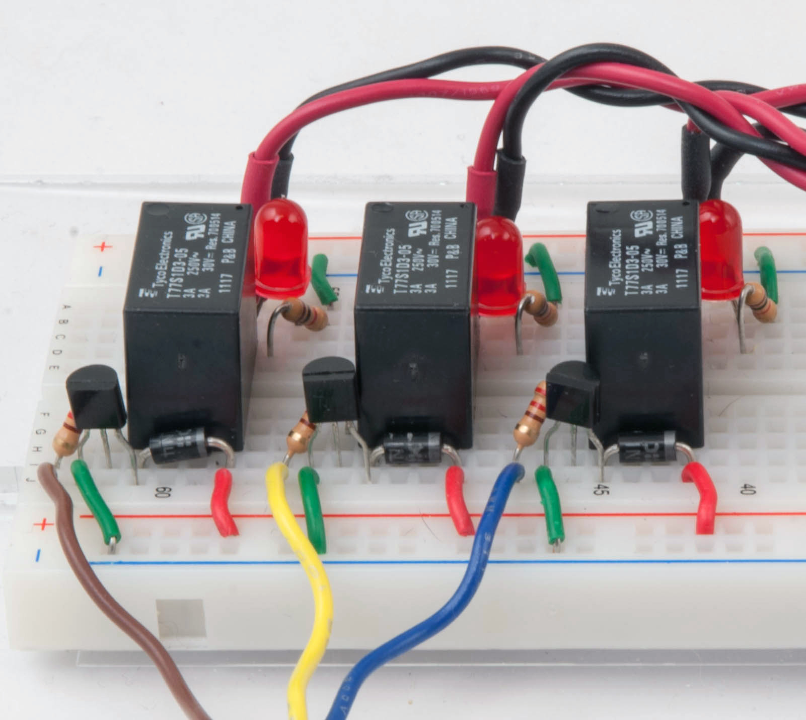
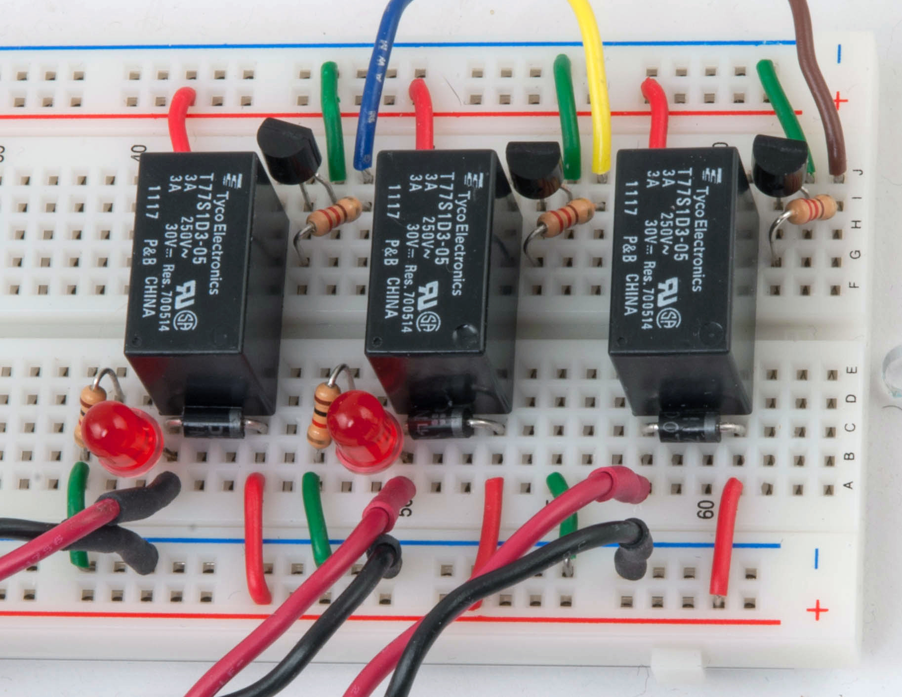
- Does this capacitor serve any other purpose than to create a smooth voltage particularly in regards to the flyback diode and transistor?
- How can the appropriate capacitance be chosen? (More specifically for a 12-volt solenoid being powered from a LiPo or portable generator)
It is crucial before selecting a solenoid valve for fuel, gas and oil shutoff to understand the basics. If you would like to know more information about solenoid valves in general, read article “Solenoid Valves…The basics” before reading on.
The solenoid valves described below are valves ASCO Numatics have identified as being suitable for Fuel, Oil and Gas applications.
Modular Gas Shut Off Solenoid Valves
- The 2/2 normally closed modular valve allows the combination of the 8214(200) solenoid valve with the V710(B) & AH(E) electro-hydraulic motorized valve
- Compact double valve design
- Ideal for the following appliances used in commercial and industrial applications
- Boilers
- Furnaces
- Ovens
- Kilns
- Heating equipment
- Gas generators
- Optional NPT threaded flange adapters are available for ease of installation and serviceability.
- Leading agency approvals
- Available in pipe connections from 3/4’’ to 3’’
Motorised Valves
- Designed for use in combustion systems
- Motorised valves are available in: 2/2 normally closed, 3/2 diversion
Features of motorised valves include:
- Pipe taps
- Visual indication
- Proof of closure
- Leading agency approvals
- Pipe connections from 3/4” to 6”.
Motorised valves are available in:
- Bronze
- Aluminium
- Cast iron
Motorised valves are rated for -40ºF service for outdoor installation in frigid climates.
ASCO Numatics produce a broad line of solenoid valves & motorized shutoff valves. The solenoid valves ASCO Numatic offer in gas and oil applications are designed to control the flow of fuel gas, liquid propane, and all other grades of fuel oil used in combustion applications such as:
- Industrial furnaces
- Ovens
- Kilns
- Incinerators
- Burners
- Boilers
Asco Solenoid Valves and their uses:
- Direct-Acting Solenoid Valves. Direct-acting solenoid valves open the orifice of a normally closed valve or close the orifice of a normally open valve when the solenoid is energised. When de-energised, a spring returns the valve to its original position. Direct-acting solenoid valves will operate at pressures from 0 psi to its rated maximum. These solenoid valves are suitable for pilot and main fuel lines.
- Internal Pilot-Operated Solenoid Valves. Internal pilot-operated solenoid valves normally have a pilot and bleed orifice, which enables them to use line pressure for operation. When the solenoid is de-energised, the pilot orifice is closed and full line pressure is applied to the top of the piston or diaphragm through the bleed orifice, providing the seating force for tight closure. When the solenoid is energised, the core opens the pilot orifice, relieving pressure from the top of the piston or diaphragm via the outlet side of the valve. The line pressure then opens the valve by lifting the diaphragm or piston off the main orifice. Internal pilot-operated valves generally are used as main shutoff valves.
- Electrohydraulic Linear-Actuated Solenoid Valves. These solenoid valves provide users with slow-opening and quick-closing operation. When energised with line voltage, the electrohydraulic actuator pumps oil from one side of a piston to another to drive the actuator stem against the valve stem and sealing member to open the valve. When line voltage is removed from the actuator, return springs in both the actuator and valve body cause the actuator piston or stem to return to its de-energised position and cause the valve stem and sealing member to return to its closed position. These solenoid valves are important for controlling the flow of fuel to the burner upon initial system startup.
Choosing the correct Solenoid Valve for your Fuel, Oil or Gas application:
It is important to clearly define specific parameters of your application for appropriate valve selection. These parameters include:
- Fuel type (gas or oil)
- Fuel viscosity (if oil)
- Ambient and fluid temperature range
- Pipe size
- Flow requirement
- Oerating pressure range
- Voltage (AC or DC)
- Required approvals (UL, FM, CSA, etc.)
- Visual or electrical
- Visual position indication
Importance in considering the media in order to find the appropriate solenoid valve for the application
For fuel gas service, generally a brass, aluminum, cast iron or steel bodied valve with nitrile rubber sealing is an appropriate choice for maximum life and performance
Natural Gas
- Compatible with aluminum, brass, cast iron or steel body materials and nitrile rubber for the valve seal material.
- Can be applied from very low pressure (inches w.c.) through to high pressure (30 psi or greater)
- Gas pressure often is used to reduce the line size of the fuel line and related components
- If your application will see ambient temperature extremes, be sure the valve is rated accordingly
- Low ambient temperatures such as -40oF (-40oC) require special low temperature elastomers for leak-tight sealing.
- High ambient temperatures may require Class H coil insulation to ensure reliable operation
Fuel Oil
- In a fuel oil system, you must consider fluid temperature (as viscosity changes with temperature), pressure and the GPM that you require
- A brass-bodied valve with Viton sealing is generally an appropriate choice for maximum life and performance
- The Viton elastomers provide a balance of material compatibility and long life
Advancements in Technology
Over the years basic solenoid valve application and design has hardly changed. However significant advancements have been made in terms of power management. Electronic technology has been integrated into new solenoid valve designs to decrease power consumption from typically 10 W to 2 W. Additional features derived from use of electronic circuits include lower temperature rise resulting in extended life of electrical components, DC operation at AC pressure, and flow ratings as well as built-in surge suppression for coil protection.
Solenoid valves and electrohydraulic-operated fuel shutoff valves have a substantial history and a bright future for individuals who define their fuel shutoff valve application requirements.
Structure diagram of the IL-IE device: 1: pump, 2: solenoid valve, 3: flow sensor, 4: pressure sensor, 5: ventilator connecting port, and 6: pneumatically operated membrane valve.


(There will be 17 connections to GPIO pins on the Raspberry Pi, 17 transistors and 17 solenoids)
I need to know how to work out the transistor needed. Also, will any 12v power supply suffice? And do I need a resistor in this circuit?
LOCAL retval AS LONG
LOCAL wvelo AS WORD ' 16 bit value
LOCAL cw AS BYTE
LOCAL param AS BYTE
IF ISFALSE velo THEN
ppHold note, %False
EXIT SUB
ELSE
ppHold note, %True
END IF
wvelo = velo * 512 ' linear mapping, for test only - range 0.2ms to 65ms
PortOut %Preg,%VeloReg
PortOut %Padr, &B11 ' A0=1, A1=1 implies command writing to 82C54
Strobe %Preg,%Veloreg,0,%StrobeLength
PortOut %Preg,%NoteReg
cw = note MOD 3
SHIFT LEFT cw,6
BIT SET cw,5
BIT SET cw,4 ' 16 bit loading - lsb first! M0, M1, M2 = 0 for mode 0 counting, BCD= 0 for 16 bit binary counting, in microsecond units
PortOut %Padr, cw
Strobe %Preg,%NoteReg,0,%Strobelength
param = note \ 3
PortOut %Preg,%SelVeloPort
PortOut %Padr, param
Strobe %Preg,%SelVeloPort,0,%StrobeLength ' now we generate a strobe such that the 74154 selects the correct timer and latches the data
PortOut %Preg, %VeloOut ' send a strobe pulse
Strobe %Preg,%VeloOut,0,%StrobeLength ' now we should send 2 bytes of timer data (the velo information in 16 bits):
PortOut %Preg,%NoteReg
PortOut %Padr, LOBYT (wvelo)
Strobe %Preg,%NoteReg,0,%StrobeLength ' set A0,A1 to the correct timer:
Portout %Preg,%VeloReg ' we use this port to select the timer adresses via A0,A1 = D0,D1
PortOut %Padr, note MOD 3 ' 0 = timer 0, 1=timer 2, 2= timer 3, 3= controll
Strobe %Preg,%VeloReg,0,%StrobeLength ' generate a strobe to latch this byte into the timer
Strobe %Preg,%SelVeloPort,0,%StrobeLength ' now once again for the MSB of the velo data:
PortOut %Preg,%NoteReg
PortOut %Padr, HIBYT (wvelo)
Strobe %Preg,%NoteReg,0,%StrobeLength
Strobe %Preg,%SelVeloPort,0,%StrobeLength ' now both lsb and msb have been sent to the timer. It should now be counting...
These board can be purchased from the Logos Laboratories. Delivery time is ca. 4 weeks. Fully assembled, a board costs 350Euros (price as of 22.09.2001). Two octave boards are around 500 Euro. Enquire by .email
TYPE Akeys BYTE ' makes a single 128-bit variable, if adressed by its pointer.
b000007 AS BYTE ' contents of latch 1
b008015 AS BYTE ' contents of latch 2
b016023 AS BYTE ' contents of latch 3
b024031 AS BYTE ' contents of latch 4
b032039 AS BYTE ' contents of latch 5
b040047 AS BYTE ' contents of latch 6
b048055 AS BYTE ' contents of latch 7
b056063 AS BYTE ' contents of latch 8
b064071 AS BYTE ' contents of latch 9
b072079 AS BYTE ' contents of latch 10
b080087 AS BYTE ' contents of latch 11
b088095 AS BYTE ' contents of latch 12
b096103 AS BYTE ' contents of latch 13
b104111 AS BYTE ' contents of latch 14
b112119 AS BYTE ' contents of latch 15
b120127 AS BYTE ' contents of latch 16
END TYPE
' bit 0 of lowest data-latch
' the note to play does not have to be passed, as each note gets a task of its own.
' the velocity is passed in Task().level
LOCAL note AS BYTE
note = 0
IF ISFALSE Task(%Toets0 + note).level THEN
' switch note off, if it was ON
IF BIT (Vkey.b000007,note) THEN ppVelo note, %False
IF BIT (Nkey.b000007,note) THEN ppHold note, %False
StopTask %Toets0 + note ' this also resets Task().tog- EXIT SUB
IF ISFALSE Task(%Toets0+ note).tog THEN
ppVelo note, %True' reschedule the task...
ReScheduleTask %Toets0 + note, Coeff(Task(%Toets0+ note).level) ' freq. is declared as single precision
Task(%Toets0+ note).tog = %True
EXIT SUB
ppVelo note, %False ' velo bit off
ppHold note, %True ' hold ON
StopTask %Toets0 + note ' note stays on until task is switched on again, with level set to zero.
SUB Toets1()
LOCAL note AS BYTE
note = 1
IF ISFALSE Task(%Toets0+ note).level THEN
IF BIT (Vkey.b000007,note MOD 8) THEN ppVelo note, %False
IF BIT (Nkey.b000007,note MOD 8) THEN ppHold note, %False
StopTask %Toets0 + note
EXIT SUB
END IF
IF ISFALSE Task(%Toets0 + note).tog THEN
ppVelo note, %True
ReScheduleTask %Toets0 + note, Coeff(Task(%Toets0 + note).level)
Task(%Toets0 + note).tog = %True
EXIT SUB
END IF
ppVelo note, %False
ppHold note, %True
LOCAL nv AS INTEGER
LOCAL noot?
LOCAL velo?
nv = GetMidiNote% (Task(%ppListen).channel, %Remove OR %Oldest)
IF nv = %NotFalse THEN
EXIT SUB
- ELSE
velo? = LOBYT (nv)
noot? = HIBYT (nv)
- END IF
ppNote noot?, velo? ' this procedure resides in gmt_lib.dll
IF velo? THEN
AddNote2Har Task(%ppListen).Har, noot?, velo?
- ELSE
DelNote2Har Task(%ppListen).Har, noot?
- END IF
END SUB
Tidak ada komentar:
Posting Komentar