
Eye Diagram Basics: Reading and applying eye diagrams
Accelerating data rates, greater design complexity, standards requirements, and shorter cycle times put greater demand on design engineers to debug complex signal integrity issues as early as possible. Because today's serial data links operate at gigahertz transmission frequencies, a host of variables can affect the integrity of signals, including transmission-line effects, impedance mismatches, signal routing, termination schemes, and grounding schemes. By using an oscilloscope to create an eye diagram, engineers can quickly evaluate system performance and gain insight into the nature of channel imperfections that can lead to errors when a receiver tries to interpret the value of a bit.
A serial digital signal can suffer impairments as it travels from a transmitter to a receiver. The transmitter, PCB traces, connectors, and cables will introduce interference that will degrade a signal both in its amplitude and timing. A signal can also suffer impairments from internal sources. For example, when signals on adjacent pairs of PCB traces or IC pins toggle, crosstalk among those signals can interfere with other signals. Thus, you need to determine at what point to place the oscilloscope probe in order to generate an eye diagram that will help you locate the source of the problem. Furthermore, where you place an oscilloscope's probe will produce differing signals on the display.
Generating an eye diagram
An eye diagram is a common indicator of the quality of signals in high-speed digital transmissions. An oscilloscope generates an eye diagram by overlaying sweeps of different segments of a long data stream driven by a master clock. The triggering edge may be positive or negative, but the displayed pulse that appears after a delay period may go either way; there is no way of knowing beforehand the value of an arbitrary bit. Therefore, when many such transitions have been overlaid, positive and negative pulses are superimposed on each other. Overlaying many bits produces an eye diagram, so called because the resulting image looks like the opening of an eye.
In an ideal world, eye diagrams would look like rectangular boxes. In reality, communications are imperfect, so the transitions do not line perfectly on top of each other, and an eye-shaped pattern results. On an oscilloscope, the shape of an eye diagram will depend upon various types of triggering signals, such as clock triggers, divided clock triggers, and pattern triggers. Differences in timing and amplitude from bit to bit cause the eye opening to shrink.
Interpreting an eye diagram
A properly constructed eye should contain every possible bit sequence from simple alternate 1’s and 0’s to isolated 1’s after long runs of 0’s, and all other patterns that may show up weaknesses in the design. Eye diagrams usually include voltage and time samples of the data acquired at some sample rate below the data rate. In Figure 1, the bit sequences 011, 001, 100, and 110 are superimposed over one another to obtain the final eye diagram.
A perfect eye diagram contains an immense amount of parametric information about a signal, like the effects deriving from physics, irrespective of how infrequently these effects occur. If a logic 1 is so distorted that the receiver at the far end can misjudge it for logic 0, you will easily discern this from an eye diagram. What you will not be able to detect, however, are logic or protocol problems, such as when a system is supposed to transmit a logic 0 but sends a logic 1, or when the logic is in conflict with a protocol.
What is jitter?
Although in theory eye diagrams should look like rectangular boxes, the finite rise and fall times of signals and oscilloscopes cause eye diagrams to actually look more like the image in Figure 2a. When high-speed digital signals are transmitted, the impairments introduced at various stages lead to timing errors. One such timing error is “jitter,” which results from the misalignment of rise and fall times (Figure 2b).
Jitter occurs when a riding or falling edges occur at times that differ from the ideal time. Some edges occur early, some occur late. In a digital circuit, all signals are transmitted in reference to clock signals. The deviation of the digital signals as a result of reflections, intersymbol interference, crosstalk, PVT (process-voltage-temperature) variations, and other factors amounts to jitter. Some jitter is simply random.
In Figure 2c, the absolute timing error or jitter margin is less than that in Figure 2b, but the eye opening in Figure 2c is smaller because of the higher bit rate. With the increase in bit rate, the absolute time error represents an increasing portion of the cycle, thus reducing the size of the eye opening. This may increase the potential for data errors.
The effect of termination is clearly visible in the eye diagrams generated. With improper termination, the eye looks constrained or stressed (Figure 3a), and with improved termination schemes, the eye becomes more relaxed (Figure 3b). A poorly terminated signal line suffers from multiple reflections. The reflected waves are of significant amplitude, which may severely constrict the eye. Typically, this is the worst-case operating condition for the receiver, and if the receiver can operate error-free in the presence of such interference, then it meets specifications.
As can be seen in Figure 4, an eye diagram can reveal important information. It can indicate the best point for sampling, divulge the SNR (signal-to-noise ratio) at the sampling point, and indicate the amount of jitter and distortion. Additionally, it can show the time variation at zero crossing, which is a measure of jitter.
A serial digital signal can suffer impairments as it travels from a transmitter to a receiver. The transmitter, PCB traces, connectors, and cables will introduce interference that will degrade a signal both in its amplitude and timing. A signal can also suffer impairments from internal sources. For example, when signals on adjacent pairs of PCB traces or IC pins toggle, crosstalk among those signals can interfere with other signals. Thus, you need to determine at what point to place the oscilloscope probe in order to generate an eye diagram that will help you locate the source of the problem. Furthermore, where you place an oscilloscope's probe will produce differing signals on the display.
Generating an eye diagram
An eye diagram is a common indicator of the quality of signals in high-speed digital transmissions. An oscilloscope generates an eye diagram by overlaying sweeps of different segments of a long data stream driven by a master clock. The triggering edge may be positive or negative, but the displayed pulse that appears after a delay period may go either way; there is no way of knowing beforehand the value of an arbitrary bit. Therefore, when many such transitions have been overlaid, positive and negative pulses are superimposed on each other. Overlaying many bits produces an eye diagram, so called because the resulting image looks like the opening of an eye.
In an ideal world, eye diagrams would look like rectangular boxes. In reality, communications are imperfect, so the transitions do not line perfectly on top of each other, and an eye-shaped pattern results. On an oscilloscope, the shape of an eye diagram will depend upon various types of triggering signals, such as clock triggers, divided clock triggers, and pattern triggers. Differences in timing and amplitude from bit to bit cause the eye opening to shrink.
Interpreting an eye diagram
A properly constructed eye should contain every possible bit sequence from simple alternate 1’s and 0’s to isolated 1’s after long runs of 0’s, and all other patterns that may show up weaknesses in the design. Eye diagrams usually include voltage and time samples of the data acquired at some sample rate below the data rate. In Figure 1, the bit sequences 011, 001, 100, and 110 are superimposed over one another to obtain the final eye diagram.
|

A perfect eye diagram contains an immense amount of parametric information about a signal, like the effects deriving from physics, irrespective of how infrequently these effects occur. If a logic 1 is so distorted that the receiver at the far end can misjudge it for logic 0, you will easily discern this from an eye diagram. What you will not be able to detect, however, are logic or protocol problems, such as when a system is supposed to transmit a logic 0 but sends a logic 1, or when the logic is in conflict with a protocol.
What is jitter?
Although in theory eye diagrams should look like rectangular boxes, the finite rise and fall times of signals and oscilloscopes cause eye diagrams to actually look more like the image in Figure 2a. When high-speed digital signals are transmitted, the impairments introduced at various stages lead to timing errors. One such timing error is “jitter,” which results from the misalignment of rise and fall times (Figure 2b).
|

Jitter occurs when a riding or falling edges occur at times that differ from the ideal time. Some edges occur early, some occur late. In a digital circuit, all signals are transmitted in reference to clock signals. The deviation of the digital signals as a result of reflections, intersymbol interference, crosstalk, PVT (process-voltage-temperature) variations, and other factors amounts to jitter. Some jitter is simply random.
In Figure 2c, the absolute timing error or jitter margin is less than that in Figure 2b, but the eye opening in Figure 2c is smaller because of the higher bit rate. With the increase in bit rate, the absolute time error represents an increasing portion of the cycle, thus reducing the size of the eye opening. This may increase the potential for data errors.
The effect of termination is clearly visible in the eye diagrams generated. With improper termination, the eye looks constrained or stressed (Figure 3a), and with improved termination schemes, the eye becomes more relaxed (Figure 3b). A poorly terminated signal line suffers from multiple reflections. The reflected waves are of significant amplitude, which may severely constrict the eye. Typically, this is the worst-case operating condition for the receiver, and if the receiver can operate error-free in the presence of such interference, then it meets specifications.
|

As can be seen in Figure 4, an eye diagram can reveal important information. It can indicate the best point for sampling, divulge the SNR (signal-to-noise ratio) at the sampling point, and indicate the amount of jitter and distortion. Additionally, it can show the time variation at zero crossing, which is a measure of jitter.
|

Eye diagrams provide instant visual data that engineers can use to check the signal integrity of a design and uncover problems early in the design process. Used in conjunction with other measurements such as bit-error rate, an eye diagram can help a designer predict performance and identify possible sources of problems.
Evolution of the eye diagram
focused on the evolution of the eye diagram: from individual signal integrity measurements to a BER bathtub that determines eye closure or Tj at a specific BER. The downside to the BER bathtub is that it solely focuses on the horizontal time/jitter closure.
The ability of a receiver to accurately discern a 1 from a 0 is dependent not only on the horizontal placement of the logic state but also on the voltage level at the decision threshold. The evolution of the eye diagram needs to take this into account for proper signal integrity characterization.
Noise decomposition (Figure 1) extends the characterization of eye diagrams to account for vertical closure. In the same sense that we can decompose T(jitter) into Rj and Dj, we can also decompose T(noise) into Rn and Dn. For BW limited systems with severe ISI, the vertical closure can sometimes dominate the BER failures and needs to be characterized.
The resultant eye diagram or BERT scan (Figure 2) is an evolution of the eye diagram to take into account not only the horizontal impairments to the eye but also the vertical impairments. It essentially combines a BER bathtub with horizontal jitter closing and a BER bathtub with vertical noise closing.
I hope that this information helps you to see how the eye diagram has evolved and how these new measurement results can help you develop a system with better signal integrity. Please don’t hesitate to post up your questions or comments.


XXX . XXX How to verify and debug next-generation memory
With the recent release of both LPDDR3 and DDR4 specifications by JEDEC, the move to the next generation of memory technologies is in full swing. First out of the gates was LPDDR3, which will replace LPDDR2 in mobile devices and ultra-thin laptops with commercial deployments beginning in 2014. Then came the new specification for synchronous DDR4, the next generation DRAM used in everything from laptops to servers that will likely start seeing production deployments in early 2015.
The trends in the new memory specs are predictable: higher speeds, increased densities, smaller packaging, and reduced power consumptions. For design engineers charged with electrical verification and debugging, the new standards bring a number of notable changes and new measurement challenges. The combination of faster speeds and lower voltage means that signal integrity is more important than ever, while denser packaging will create signal access challenges.
This article highlights the changes these new standards bring to electrical verification and describes how to prepare for proper signal access to LPDDR3 and DDR4 memory systems. It will also look at instrument selection and techniques needed for performing electrical verification tests on these emerging standards.
LPDDR3 Overview
In May of 2012, JEDEC published the JESD209-3 Low Power Memory Device Standard. In comparison to LPDDR2, LPDDR3 offers a higher data rate, greater bandwidth and power efficiency, and higher memory density. LPDDR3 achieves a data rate of 1600 MT/s and uses a number of new technologies, including write-leveling and command/address training, optional on-die termination (ODT), and low-I/O capacitance.
As with LPDDR2, LPDDR3 supports both package-on-package and discrete packaging types to meet the requirements of various mobile devices, and it offers designers the ability to select the options that best meet the needs of their product. LPDDR3 preserves the power-efficient features and signaling interface of LPDDR2, allowing for fast clock stop/start, low-power self-refresh, and smart array management.
From an electrical verification perspective, LPDDR3 is pushing the system power envelope with its combination of lower operating voltage and higher bandwidths. By comparison, first-generation LPDDR ran at 200 MHz at 1.8V. With LPDDR2 voltage dropped to 1.2V while speed increased to 533 MHz. Now LPDDR3 calls for the same 1.2V but runs at 800 MHz. This means that signal integrity will be an important factor in order to verify clock cycles on shorter 1.25 ns clock periods. Table 1 shows a comparison between the two generations, indicating the need for higher bandwidth oscilloscopes to maintain signal integrity.

DDR4 Overview
Released in September of 2012, the DDR4 specification calls for greater performance, significantly increased packaging density, improved reliability and lower power consumption compared to DDR3. As shown in Table 2, voltages drop to 1.2V from 1.5V to reduce power consumption while the performance factor nearly doubles to 3,200 MT/sec. (megatransfers per second). Other changes include higher densities to support memory-intensive server applications, higher data rates and the ability to stack pins for higher density module placement.

From a test perspective, as with LPDDRR3, the move to higher transfer rates and lower voltages will increase the emphasis on signal integrity and timing and margin measurements for validating memory technologies. To accommodate the increased measurement complexity, JEDEC is making a number of changes and updates to required test methodology.
One of the most significant changes is the proposed requirement to establish the reference voltage or V center used for compliance testing using a variable approach. For DDR3, this value was fixed at 750 mV. The new approach involves making multiple acquisitions of the output data (DQ) and a data strobe signal (DQS) Write burst. The largest to smallest voltage value for each is then measured and an average created using a simple formula. This then becomes the DQ voltage reference for centering and making reference measurements using an eye diagram. This process is shown in Figure 1.

Another notable change in DDR4 testing is the expanded use of eye diagrams. The proposed test specification will set required eye height and width and will provide guidance on what will be considered a deterministic level of performance from a timing perspective. It will also set margin requirements with random or Gaussian noise applied to the measurement. Figure 2 shows the eye diagram for DQ from the DD4 spec with recommended mask sizing that is placed on the Vref center.

Following the lead of many serial standards, DDR4 will now incorporate a statistical jitter measurement approach for speeds greater than 2133. For speeds under 2133, all jitter will be assumed to be deterministic jitter (DJ). For 2133 and above, tests will look at both DJ and random jitter (RJ). To date, many of the timing parameters for jitter have not been published, but designers should be aware that jitter testing will be a requirement. One benefit of expanded jitter testing in DDR4 is that should devices fail to meet jitter requirements, the test and measurement vendor community offers robust jitter decomposition tools that can help isolate the source of problems.
In addition, JEDEC will no longer require de-rating of pass/fail limits for setup and hold measurement based on signal slew rate, as was the case with DDR2 and DDR3. In discussing the issue with engineers, the JEDEC standards committee found that the complex de-rating procedure was poorly understood and rarely performed. Typically, most engineers relied on making standard slew rate measurements. In DDR4, this has been replaced with the Vref averaging and eye-mask measurements described above.
The trends in the new memory specs are predictable: higher speeds, increased densities, smaller packaging, and reduced power consumptions. For design engineers charged with electrical verification and debugging, the new standards bring a number of notable changes and new measurement challenges. The combination of faster speeds and lower voltage means that signal integrity is more important than ever, while denser packaging will create signal access challenges.
This article highlights the changes these new standards bring to electrical verification and describes how to prepare for proper signal access to LPDDR3 and DDR4 memory systems. It will also look at instrument selection and techniques needed for performing electrical verification tests on these emerging standards.
LPDDR3 Overview
In May of 2012, JEDEC published the JESD209-3 Low Power Memory Device Standard. In comparison to LPDDR2, LPDDR3 offers a higher data rate, greater bandwidth and power efficiency, and higher memory density. LPDDR3 achieves a data rate of 1600 MT/s and uses a number of new technologies, including write-leveling and command/address training, optional on-die termination (ODT), and low-I/O capacitance.
As with LPDDR2, LPDDR3 supports both package-on-package and discrete packaging types to meet the requirements of various mobile devices, and it offers designers the ability to select the options that best meet the needs of their product. LPDDR3 preserves the power-efficient features and signaling interface of LPDDR2, allowing for fast clock stop/start, low-power self-refresh, and smart array management.
From an electrical verification perspective, LPDDR3 is pushing the system power envelope with its combination of lower operating voltage and higher bandwidths. By comparison, first-generation LPDDR ran at 200 MHz at 1.8V. With LPDDR2 voltage dropped to 1.2V while speed increased to 533 MHz. Now LPDDR3 calls for the same 1.2V but runs at 800 MHz. This means that signal integrity will be an important factor in order to verify clock cycles on shorter 1.25 ns clock periods. Table 1 shows a comparison between the two generations, indicating the need for higher bandwidth oscilloscopes to maintain signal integrity.
Table 1 – Faster speeds with LPDDR3 require greater oscilloscope bandwidth.
DDR4 Overview
Released in September of 2012, the DDR4 specification calls for greater performance, significantly increased packaging density, improved reliability and lower power consumption compared to DDR3. As shown in Table 2, voltages drop to 1.2V from 1.5V to reduce power consumption while the performance factor nearly doubles to 3,200 MT/sec. (megatransfers per second). Other changes include higher densities to support memory-intensive server applications, higher data rates and the ability to stack pins for higher density module placement.
Table 2 – The DDR4 specification calls for faster transfers, higher densities and lower power consumption compared to DDR3.
From a test perspective, as with LPDDRR3, the move to higher transfer rates and lower voltages will increase the emphasis on signal integrity and timing and margin measurements for validating memory technologies. To accommodate the increased measurement complexity, JEDEC is making a number of changes and updates to required test methodology.
One of the most significant changes is the proposed requirement to establish the reference voltage or V center used for compliance testing using a variable approach. For DDR3, this value was fixed at 750 mV. The new approach involves making multiple acquisitions of the output data (DQ) and a data strobe signal (DQS) Write burst. The largest to smallest voltage value for each is then measured and an average created using a simple formula. This then becomes the DQ voltage reference for centering and making reference measurements using an eye diagram. This process is shown in Figure 1.
Figure 1 – Early DDR4 verification proposals indicate a variable approach to establishing the reference voltage or V center.
Another notable change in DDR4 testing is the expanded use of eye diagrams. The proposed test specification will set required eye height and width and will provide guidance on what will be considered a deterministic level of performance from a timing perspective. It will also set margin requirements with random or Gaussian noise applied to the measurement. Figure 2 shows the eye diagram for DQ from the DD4 spec with recommended mask sizing that is placed on the Vref center.
Figure 2 –The proposed DDR4 specification adds eye diagram requirements.
Following the lead of many serial standards, DDR4 will now incorporate a statistical jitter measurement approach for speeds greater than 2133. For speeds under 2133, all jitter will be assumed to be deterministic jitter (DJ). For 2133 and above, tests will look at both DJ and random jitter (RJ). To date, many of the timing parameters for jitter have not been published, but designers should be aware that jitter testing will be a requirement. One benefit of expanded jitter testing in DDR4 is that should devices fail to meet jitter requirements, the test and measurement vendor community offers robust jitter decomposition tools that can help isolate the source of problems.
In addition, JEDEC will no longer require de-rating of pass/fail limits for setup and hold measurement based on signal slew rate, as was the case with DDR2 and DDR3. In discussing the issue with engineers, the JEDEC standards committee found that the complex de-rating procedure was poorly understood and rarely performed. Typically, most engineers relied on making standard slew rate measurements. In DDR4, this has been replaced with the Vref averaging and eye-mask measurements described above.
XXX . XXX 4%zero null How much RAM (random access memory) does a human brain have?
Working memory is not equivalent to RAM. While limitations in working memory is something we may occasionally face, it’s really not a blocking issue for most people, like it is for a computer. Although, working memory limitations can certainly be annoying when trying to remember a phone number, taking a person’s order without a notepad, or juggling 10 requests at once.
RAM on the other hand is used to load up pretty much everything you are actively working on, all the applications, browser windows and plenty of other stuff, as to be accessible as quickly as possible without the need to read from a disk. When it runs out, it causes serious performance issues for the computer.
To illustrate, look at the memory requirements on my brain when writing this answer.
While I am writing, my mind doesn’t need to “load up” anything. I simply have immediate access to all the contents in my brain, the entire time I am writing.
I can recall all the articles I’ve read on the topic, I can synthesize what I know of biology, neurology, computer science and creative writing. Combining that with my knowledge of English, written communication mixed with touch typing, eye sight and vocalizing (I often read my posts out-loud before posting) I generate the answer.
I then review and edit what I’ve written.
Oh, my dogs want to come inside. Now I access my muscle memory. I’ve just stood up, opened the door, let them in, closed the door and sat back down. It was an epic use of my entire body! Now I can continue exactly where I left off.
Comparing it like this, the human brain has pretty much an amount of RAM, because pretty much everything we’ve ever known is available to us all the time.
Side note: The attempts to calculate how much “memory” the human brain has by estimating the neurons, is not useful and wildly inaccurate.
Extensive use of any part of the mind leads to thickening of that part of the brain. Neurons are constantly created.
If a person spends their entire life learning, languages, new hobbies and activities, etc., they will continually increase the number of connections and the number of neurons. As far as is useful, there simply is no limit to the size of our minds and there will never be a way to find if there is a limit.
The human brain does not have RAM, nor does it have anything exactly comparable.
The closest analog to RAM in the human brain might be what is called “working memory” or “short term memory.”
The capacity of working memory is difficult to quantify, but cognitive scientists measure its capacity at “7 +/- 2 items.”
But what is an item?
An item is anything that can be held in working memory, so the definition is a bit circular. An item could be a word, a name, a number, or a concept. With “chunking,” an item could be a set of related concepts, so “the three little pigs” or “1 2 3” or “red white and blue” might be one chunked item or maybe two.
Working memory is for concepts. Vision seems to have its own type of short term memory, called visual short term memory (VSTM), and its capacity seems to be 3 - 5 items, where an item is something within the visual field that can be seen or noticed.
Most computational neuroscientists tend to estimate human storage capacity somewhere between 10 terabytes and 100 terabytes, though the full spectrum of guesses ranges from 1 terabyte to 2.5 petabytes. (One terabyte is equal to about 1,000 gigabytes or about 1 million megabytes; a petabyte is about 1,000 terabytes.)
The math behind these estimates is fairly simple. The human brain contains roughly 100 billion neurons. Each of these neurons seems capable of making around 1,000 connections, representing about 1,000 potential synapses, which largely do the work of data storage. Multiply each of these 100 billion neurons by the approximately 1,000 connections it can make, and you get 100 trillion data points, or about 100 terabytes of information.
Can you grow new brain cells?
The science of neurogenesis suggests it's possible to create neurons that improve your memory and thinking skills.

There are many aspects of aging you cannot prevent, but surprisingly, memory trouble is not one of them.
"The dogma for the longest time was that adult brains couldn't generate any new brain cells. "But the reality is that everyone has the capacity to develop new cells that can help enhance cognitive functions."
XXX , XXX 4%zero null 0 Resistive random-access memory
Resistive random-access memory (RRAM or ReRAM) is a type of non-volatile (NV) random-access (RAM) computer memory that works by changing the resistance across a dielectric solid-state material often referred to as a memristor. This technology bears some similarities to conductive-bridging RAM (CBRAM), and phase-change memory (PCM).
CBRAM involves one electrode providing ions that dissolve readily in an electrolyte material, while PCM involves generating sufficient Joule heating to effect amorphous-to-crystalline or crystalline-to-amorphous phase changes. On the other hand, RRAM involves generating defects in a thin oxide layer, known as oxygen vacancies (oxide bond locations where the oxygen has been removed), which can subsequently charge and drift under an electric field. The motion of oxygen ions and vacancies in the oxide would be analogous to the motion of electrons and holes in a semiconductor.
RRAM is currently under development by a number of companies, some of which have filed patent applications claiming various implementations of this technology. RRAM has entered commercialization on an initially limited KB-capacity scale.
Although anticipated as a replacement technology for flash memory, the cost benefit and performance benefit of RRAM have not been enough for companies to proceed with the replacement. A broad range of materials apparently can potentially be used for RRAM. However, the discovery[5] that the popular high-κ gate dielectric HfO2 can be used as a low-voltage RRAM has greatly encouraged others to investigate many other possibilities. Among others, SiOx has been identified to offer significant benefits. Weebit-Nano Ltd is one company that is pursuing SiOx and has already demonstrated functional devices.
In February 2012, Rambus bought an RRAM company called Unity Semiconductor for $35 million.[6] Panasonic launched an RRAM evaluation kit in May 2012, based on a tantalum oxide 1T1R (1 transistor – 1 resistor) memory cell architecture.[7]
In 2013, Crossbar introduced an RRAM prototype as a chip about the size of a postage stamp that could store 1 TB of data. In August 2013, the company claimed that large-scale production of their RRAM chips was scheduled for 2015.[8] The memory structure (Ag/a-Si/Si) closely resembles a silver-based CBRAM.
Different forms of RRAM have been disclosed, based on different dielectric materials, spanning from perovskites to transition metal oxides to chalcogenides. Silicon dioxide was shown to exhibit resistive switching as early as 1967,[9] and has recently been revisited.[10][11]
Leon Chua argued that all two-terminal non-volatile memory devices including RRAM should be considered memristors.[12] Stan Williams of HP Labs also argued that RRAM was a memristor.[13] However, others challenged this terminology and the applicability of memristor theory to any physically realizable device is open to question.[14][15] Whether redox-based resistively switching elements (RRAM) are covered by the current memristor theory is disputed.[16]
Silicon oxide presents an interesting case of resistance switching. Two distinct modes of intrinsic switching have been reported - surface-based, in which conductive silicon filaments are generated at exposed edges (which may be internal - within pores - or external - on the surface of mesa structures), and bulk switching, in which oxygen vacancy filaments are generated within the bulk of the oxide. The former mode suffers from oxidation of the filaments in air, requiring hermetic sealing to enable switching. The latter requires no sealing. In 2014 researchers from Rice University announced a silicon filament-based device that used a porous silicon oxide dielectric with no external edge structure - rather, filaments were formed at internal edges within pores. Devices can be manufactured at room temperature and have a sub-2V forming voltage, high on-off ratio, low power consumption, nine-bit capacity per cell, high switching speeds and good endurance. Problems with their inoperability in air can be overcome by hermetic sealing of devices[17]. Bulk switching in silicon oxide, pioneered by researchers at UCL (University College London) since 2012[18], offers low electroforming voltages (2.5V), switching voltages around 1V, switching times in the nanoseconds regime, and more than 10,000,000 cycles without device failure - all in ambient conditions.[19]
Forming

The basic idea is that a dielectric, which is normally insulating, can be made to conduct through a filament or conduction path formed after application of a sufficiently high voltage.[20] The conduction path can arise from different mechanisms, including vacancy or metal defect migration. Once the filament is formed, it may be reset (broken, resulting in high resistance) or set (re-formed, resulting in lower resistance) by another voltage. Many current paths, rather than a single filament, are possibly involved.[21] The presence of these current paths in the dielectric can be in situ demonstrated via conductive atomic force microscopy.[20][22][23][24]
The low-resistance path can be either localized (filamentary) or homogeneous. Both effects can occur either throughout the entire distance between the electrodes or only in proximity to one of the electrodes. Filamentary and homogenous switching effects can be distinguished by measuring the area dependence of the low-resistance state.[25]
Under certain conditions, the forming operation may be bypassed.[26] It is expected that under these conditions, the initial current is already quite high compared to insulating oxide layers.
CBRAM cells generally would not require forming if Cu ions are already present in the electrolyte, having already been driven-in by a designed photo-diffusion or annealing process; such cells may also readily return to their initial state.[27] In the absence of such Cu initially being in the electrolyte, the voltage would still be applied directly to the electrolyte, and forming would be a strong possibility.[28]
Operation styles
For random-access type memories, a 1T1R (one transistor, one resistor) architecture is preferred because the transistor isolates current to cells that are selected from cells that are not. On the other hand, a cross-point architecture is more compact and may enable vertically stacking memory layers, ideally suited for mass-storage devices. However, in the absence of any transistors, isolation must be provided by a "selector" device, such as a diode, in series with the memory element or by the memory element itself. Such isolation capabilities are inferior to the use of transistors if the on/off ratio for the selector is not sufficient, limiting the ability to operate very large arrays in this architecture. Thin film based threshold switch can work as a selector for bipolar and unipolar RRAM. Threshold switch-based selector was demonstrated for 64 Mb array. However, One shouldn't forget that the cross-point architecture requires BEOL compatible two terminal selectors like punch-through diode for bipolar RRAM or PIN diode for unipolar RRAM.
Polarity can be either binary or unary. Bipolar effects cause polarity to reverse when switching from low to high resistance (reset operation) compared to switching high to low (set operation). Unipolar switching leaves polarity unaffected, but uses different voltages.
Material systems for resistive memory cells
Multiple inorganic and organic material systems display thermal or ionic resistive switching effects. These can be grouped into the following categories:
- phase-change chalcogenides such as Ge
2Sb
2Te
5 or AgInSbTe - binary transition metal oxides such as NiO or TiO
2 - perovskites such as Sr(Zr)TiO
3 or PCMO - solid-state electrolytes such as GeS, GeSe, SiO
x or Cu
2S - organic charge-transfer complexes such as CuTCNQ
- organic donor–acceptor systems such as Al AIDCN
- two dimensional (layered) insulating materials like hexagonal boron nitride
Demonstrations
Papers at the IEDM Conference in 2007 suggested for the first time that RRAM exhibits lower programming currents than PRAM or MRAM without sacrificing programming performance, retention or endurance. Some commonly cited ReRAM systems are described further below.
HfO2-based RRAM
At IEDM 2008, the highest-performance RRAM technology to date was demonstrated by ITRI using HfO2 with a Ti buffer layer, showing switching times less than 10 ns and currents less than 30μA. At IEDM 2010, ITRI again broke the speed record, showing <0.3 ns switching time, while also showing process and operation improvements to allow yield up to 100% and endurance up to 10 billion cycles. IMEC presented updates of their RRAM program at the 2012 Symposia on VLSI Technology and Circuits, including a solution with a 500 nA operating current.
ITRI had focused on the Ti/HfO2 system since its first publication in 2008. ITRI's patent 8362454 has since been sold to TSMC; the number of prior licensees is unknown. On the other hand, IMEC focused mainly on Hf/HfO2. Winbond had done more recent work toward advancing and commercializing the HfO2-based RRAM.
Panasonic
Panasonic revealed its TaOx-based ReRAM at IEDM 2008. A key requirement was the need for a high work function metal such as Pt or Ir to interface with the TaOx layer. The change of O content results in resistance change as well as Schottky barrier change. More recently, a Ta2O5/TaOx layer was implemented, which still requires the high work function metal to interface with Ta2O5.[41] This system has been associated with high endurance demonstration (trillion cycles),[42] but products are specified at 100K cycles.[43] Filament diameters as large as ~100 nm have been observed.[44] Panasonic released a 4Mb part with Fujitsu,[45] and is developing 40nm embedded memory with UMC.
HP Memristor
On 30 April 2008, HP announced that they had discovered the memristor, originally envisioned as a missing 4th fundamental circuit element by Chua in 1971. On 8 July they announced they would begin prototyping RRAM using their memristors.[47] HP first demonstrated its memristor using TiOx,[48] but later migrated to TaOx,[49] possibly due to improved stability.[50] The TaOx-based device has some material similarity to Panasonic's ReRAM, but the operation characteristics are different. The Hf/HfOx system was similarly studied.[51]
Adesto Technologies
Adesto Technologies' ReRAM is based on filaments generated from the electrode metal rather than oxygen vacancies. The original material system was Ag/GeS2[52] but eventually migrated to ZrTe/Al2O3.[53] The tellurium filament achieved better stability as compared to silver. Adesto has targeted the ultralow power memory for Internet-of-Things (IoT) applications. Adesto has released products manufactured at Altis foundry[54] and entered into a 45nm foundry agreement with TowerJazz/Panasonic.
Crossbar
Crossbar implements an Ag filament in amorphous Si along with a threshold switching system to achieve a diode+ReRAM.[56][57] Their system includes the use of a transistor in 1T1R or 1TNR architecture. Crossbar started producing samples at SMIC on the 40nm process in 2017.[58] The Ag filament diameter has been visualized on the scale of tens of nanometers.
Programmable metallization cell
Infineon Technologies calls it conductive-bridging RAM(CBRAM), NEC has a variant called “Nanobridge” and Sony calls their version “electrolytic memory”. New research suggests CBRAM can be 3D printed[
ReRam test boards
- Panasonic AM13L-STK2 : MN101LR05D 8-bit MCU with built in ReRAM for evaluation, USB 2.0 connector
Future applications
Compared to PRAM, RRAM operates at a faster timescale (switching time can be less than 10 ns), while compared to MRAM, it has a simpler, smaller cell structure (less than 8F² MIM stack). A vertical 1D1R (one diode, one resistive switching device) integration can be used for crossbar memory structure to reduce the unit cell size to 4F² (F is the feature dimension).[62] Compared to flash memory and racetrack memory, a lower voltage is sufficient, and hence it can be used in low-power applications. Also, due to its relatively small access latency and high density, RRAM is considered a promising candidate for designing caches.
ITRI has shown that RRAM is scalable below 30 nm. The motion of oxygen atoms is a key phenomenon for oxide-based RRAM; one study indicated that oxygen motion may take place in regions as small as 2 nm.[66] It is believed that if a filament is responsible, it would not exhibit direct scaling with cell size.[67] Instead, the current compliance limit (set by an outside resistor, for example) could define the current-carrying capacity of the filament.
A significant hurdle to realizing the potential of RRAM is the sneak path problem that occurs in larger passive arrays. In 2010, complementary resistive switching (CRS) was introduced as a possible solution to sneak-path current interference.[69] In the CRS approach, the information storing states are pairs of high- and low-resistance states (HRS/LRS and LRS/HRS) so that the overall resistance is always high, allowing larger passive crossbar arrays.
A drawback to the initial CRS solution is the requirement for switching endurance caused by conventional destructive readout based on current measurements. A new approach for a nondestructive readout based on capacity measurement potentially lowers the requirements for both material endurance and power consumption. Bi-layer structure is used to produce the nonlinearity in LRS to avoid the sneak path problem. A single-layer device exhibiting a strong nonlinear conduction in LRS was reported. Another bi-layer structure was introduced for bipolar RRAM to improve the HRS and stability.
Another solution to the sneak current issue is to perform read and reset operations in parallel across an entire row of cells, while using set on selected cells.In this case, for a 3D-RRAM 1TNR array, with a column of N RRAM cells situated above a select transistor, only the intrinsic nonlinearity of the HRS is required to be sufficiently large, since the number of vertical levels N is limited (e.g., N = 8–32), and this has been shown possible for a low-current RRAM system.
Modeling of 2D and 3D caches designed with RRAM and other non-volatile random access memories such as MRAM and PCM can be done using DESTINY tool.
How RAM Works
Random access memory (RAM) is the best known form of computer memory. RAM is considered "random access" because you can access any memory cell directly if you know the row and column that intersect at that cell.
The opposite of RAM is serial access memory (SAM). SAM stores data as a series of memory cells that can only be accessed sequentially (like a cassette tape). If the data is not in the current location, each memory cell is checked until the needed data is found. SAM works very well for memory buffers, where the data is normally stored in the order in which it will be used (a good example is the texture buffer memory on a video card). RAM data, on the other hand, can be accessed in any order.
Similar to a microprocessor, a memory chip is an integrated circuit (IC) made of millions of transistors and capacitors. In the most common form of computer memory, dynamic random access memory (DRAM), a transistor and a capacitor are paired to create a memory cell, which represents a single bit of data. The capacitor holds the bit of information -- a 0 or a 1 (see How Bits and Bytes Work for information on bits). The transistor acts as a switch that lets the control circuitry on the memory chip read the capacitor or change its state.
A capacitor is like a small bucket that is able to store electrons. To store a 1 in the memory cell, the bucket is filled with electrons. To store a 0, it is emptied. The problem with the capacitor's bucket is that it has a leak. In a matter of a few milliseconds a full bucket becomes empty. Therefore, for dynamic memory to work, either the CPU or the memory controller has to come along and recharge all of the capacitors holding a 1 before they discharge. To do this, the memory controller reads the memory and then writes it right back. This refresh operation happens automatically thousands of times per second.
The capacitor in a dynamic RAM memory cell is like a leaky bucket. It needs to be refreshed periodically or it will discharge to 0. This refresh operation is where dynamic RAM gets its name. Dynamic RAM has to be dynamically refreshed all of the time or it forgets what it is holding. The downside of all of this refreshing is that it takes time and slows down the memory.
In this article, you'll learn all about what RAM is, what kind you should buy and how to install it.
Memory is made up of bits arranged in a two-dimensional grid.
In this figure, red cells represent 1s and white cells represent 0s. In the animation, a column is selected and then rows are charged to write data into the specific column.
Memory cells are etched onto a silicon wafer in an array of columns (bitlines) and rows (wordlines). The intersection of a bitline and wordline constitutes the address of the memory cell.
DRAM works by sending a charge through the appropriate column (CAS) to activate the transistor at each bit in the column. When writing, the row lines contain the state the capacitor should take on. When reading, the sense-amplifier determines the level of charge in the capacitor. If it is more than 50 percent, it reads it as a 1; otherwise it reads it as a 0. The counter tracks the refresh sequence based on which rows have been accessed in what order. The length of time necessary to do all this is so short that it is expressed in nanoseconds (billionths of a second). A memory chip rating of 70ns means that it takes 70 nanoseconds to completely read and recharge each cell.
Memory cells alone would be worthless without some way to get information in and out of them. So the memory cells have a whole support infrastructure of other specialized circuits. These circuits perform functions such as:
- Identifying each row and column (row address select and column address select)
- Keeping track of the refresh sequence (counter)
- Reading and restoring the signal from a cell (sense amplifier)
- Telling a cell whether it should take a charge or not (write enable)
Other functions of the memory controller include a series of tasks that include identifying the type, speed and amount of memory and checking for errors.
Static RAM is fast and expensive, and dynamic RAM is less expensive and slower. So static RAM is used to create the CPU's speed-sensitive cache, while dynamic RAM forms the larger system RAM space.
Memory chips in desktop computers originally used a pin configuration called dual inline package (DIP). This pin configuration could be soldered into holes on the computer's motherboard or plugged into a socket that was soldered on the motherboard. This method worked fine when computers typically operated on a couple of megabytes or less of RAM, but as the need for memory grew, the number of chips needing space on the motherboard increased.
The solution was to place the memory chips, along with all of the support components, on a separate printed circuit board (PCB) that could then be plugged into a special connector (memory bank) on the motherboard. Most of these chips use a small outline J-lead (SOJ) pin configuration, but quite a few manufacturers use the thin small outline package (TSOP) configuration as well. The key difference between these newer pin types and the original DIP configuration is that SOJ and TSOP chips are surface-mounted to the PCB. In other words, the pins are soldered directly to the surface of the board, not inserted in holes or sockets.
Memory chips are normally only available as part of a card called a module. You've probably seen memory listed as 8x32 or 4x16. These numbers represent the number of the chips multiplied by the capacity of each individual chip, which is measured in megabits (Mb), or one million bits. Take the result and divide it by eight to get the number of megabytes on that module. For example, 4x32 means that the module has four 32-megabit chips. Multiply 4 by 32 and you get 128 megabits. Since we know that a byte has 8 bits, we need to divide our result of 128 by 8. Our result is 16 megabytes!
The following are some common types of RAM:
- SRAM: Static random access memory uses multiple transistors, typically four to six, for each memory cell but doesn't have a capacitor in each cell. It is used primarily for cache.
- DRAM: Dynamic random access memory has memory cells with a paired transistor and capacitor requiring constant refreshing.
- FPM DRAM: Fast page mode dynamic random access memory was the original form of DRAM. It waits through the entire process of locating a bit of data by column and row and then reading the bit before it starts on the next bit. Maximum transfer rate to L2 cache is approximately 176 MBps.
- EDO DRAM: Extended data-out dynamic random access memory does not wait for all of the processing of the first bit before continuing to the next one. As soon as the address of the first bit is located, EDO DRAM begins looking for the next bit. It is about five percent faster than FPM. Maximum transfer rate to L2 cache is approximately 264 MBps.
- SDRAM: Synchronous dynamic random access memory takes advantage of the burst mode concept to greatly improve performance. It does this by staying on the row containing the requested bit and moving rapidly through the columns, reading each bit as it goes. The idea is that most of the time the data needed by the CPU will be in sequence. SDRAM is about five percent faster than EDO RAM and is the most common form in desktops today. Maximum transfer rate to L2 cache is approximately 528 MBps.
- DDR SDRAM: Double data rate synchronous dynamic RAM is just like SDRAM except that is has higher bandwidth, meaning greater speed. Maximum transfer rate to L2 cache is approximately 1,064 MBps (for DDR SDRAM 133 MHZ).
- RDRAM: Rambus dynamic random access memory is a radical departure from the previous DRAM architecture. Designed by Rambus, RDRAM uses a Rambus in-line memory module (RIMM), which is similar in size and pin configuration to a standard DIMM. What makes RDRAM so different is its use of a special high-speed data bus called the Rambus channel. RDRAM memory chips work in parallel to achieve a data rate of 800 MHz, or 1,600 MBps. Since they operate at such high speeds, they generate much more heat than other types of chips. To help dissipate the excess heat Rambus chips are fitted with a heat spreader, which looks like a long thin wafer. Just like there are smaller versions of DIMMs, there are also SO-RIMMs, designed for notebook computers.
- Credit Card Memory: Credit card memory is a proprietary self-contained DRAM memory module that plugs into a special slot for use in notebook computers.
- PCMCIA Memory Card: Another self-contained DRAM module for notebooks, cards of this type are not proprietary and should work with any notebook computer whose system bus matches the memory card's configuration.
- CMOS RAM: CMOS RAM is a term for the small amount of memory used by your computer and some other devices to remember things like hard disk settings -- see Why does my computer need a battery? for details. This memory uses a small battery to provide it with the power it needs to maintain the memory contents.
- VRAM: VideoRAM, also known as multiport dynamic random access memory (MPDRAM), is a type of RAM used specifically for video adapters or 3-D accelerators. The "multiport" part comes from the fact that VRAM normally has two independent access ports instead of one, allowing the CPU and graphics processor to access the RAM simultaneously. VRAM is located on the graphics card and comes in a variety of formats, many of which are proprietary. The amount of VRAM is a determining factor in the resolution and color depth of the display. VRAM is also used to hold graphics-specific information such as 3-D geometry data and texture maps. True multiport VRAM tends to be expensive, so today, many graphics cards use SGRAM (synchronous graphics RAM) instead. Performance is nearly the same, but SGRAM is cheaper.
The type of board and connector used for RAM in desktop computershas evolved over the past few years. The first types were proprietary, meaning that different computer manufacturers developed memory boards that would only work with their specific systems. Then came SIMM, which stands for single in-line memory module. This memory board used a 30-pin connector and was about 3.5 x .75 inches in size (about 9 x 2 cm). In most computers, you had to install SIMMs in pairs of equal capacity and speed. This is because the width of the bus is more than a single SIMM. For example, you would install two 8-megabyte (MB) SIMMs to get 16 megabytes total RAM. Each SIMM could send 8 bits of data at one time, while the system bus could handle 16 bits at a time. Later SIMM boards, slightly larger at 4.25 x 1 inch (about 11 x 2.5 cm), used a 72-pin connector for increased bandwidth and allowed for up to 256 MB of RAM.
As processors grew in speed and bandwidth capability, the industry adopted a new standard in dual in-line memory module (DIMM). With a whopping 168-pin or 184-pin connector and a size of 5.4 x 1 inch (about 14 x 2.5 cm), DIMMs range in capacity from 8 MB to 1 GB per module and can be installed singly instead of in pairs. Most PC memory modules and the modules for the Mac G5 systems operate at 2.5 volts, while older Mac G4 systems typically use 3.3 volts. Another standard, Rambus in-line memory module (RIMM), is comparable in size and pin configuration to DIMM but uses a special memory bus to greatly increase speed.

Many brands of notebook computers use proprietary memory modules, but several manufacturers use RAM based on the small outline dual in-line memory module (SODIMM) configuration. SODIMM cards are small, about 2 x 1 inch (5 x 2.5 cm), and have 144 or 200 pins. Capacity ranges from 16 MB to 1 GB per module. To conserve space, the Apple iMac desktop computer uses SODIMMs instead of the traditional DIMMs. Sub-notebook computers use even smaller DIMMs, known as MicroDIMMs, which have either 144 pins or 172 pins.
Most memory available today is highly reliable. Most systems simply have the memory controller check for errors at start-up and rely on that. Memory chips with built-in error-checking typically use a method known as parity to check for errors. Parity chips have an extra bit for every 8 bits of data. The way parity works is simple. Let's look at even parity first.
When the 8 bits in a byte receive data, the chip adds up the total number of 1s. If the total number of 1s is odd, the parity bit is set to 1. If the total is even, the parity bit is set to 0. When the data is read back out of the bits, the total is added up again and compared to the parity bit. If the total is odd and the parity bit is 1, then the data is assumed to be valid and is sent to the CPU. But if the total is odd and the parity bit is 0, the chip knows that there is an error somewhere in the 8 bits and dumps the data. Odd parity works the same way, but the parity bit is set to 1 when the total number of 1s in the byte are even.
The problem with parity is that it discovers errors but does nothing to correct them. If a byte of data does not match its parity bit, then the data are discarded and the system tries again. Computers in critical positions need a higher level of fault tolerance. High-end servers often have a form of error-checking known as error-correction code (ECC). Like parity, ECC uses additional bits to monitor the data in each byte. The difference is that ECC uses several bits for error checking -- how many depends on the width of the bus -- instead of one. ECC memory uses a special algorithm not only to detect single bit errors, but actually correct them as well. ECC memory will also detect instances when more than one bit of data in a byte fails. Such failures are very rare, and they are not correctable, even with ECC.
The majority of computers sold today use nonparity memory chips. These chips do not provide any type of built-in error checking, but instead rely on the memory controller for error detection.
It's been said that you can never have enough money, and the same holds true for RAM, especially if you do a lot of graphics-intensive work or gaming. Next to the CPU itself, RAM is the most important factor in computer performance. If you don't have enough, adding RAM can make more of a difference than getting a new CPU!
If your system responds slowly or accesses the hard drive constantly, then you need to add more RAM. If you are running Windows XP, Microsoft recommends 128MB as the minimum RAM requirement. At 64MB, you may experience frequent application problems. For optimal performance with standard desktop applications, 256MB is recommended. If you are running Windows 95/98, you need a bare minimum of 32 MB, and your computer will work much better with 64 MB. Windows NT/2000 needs at least 64 MB, and it will take everything you can throw at it, so you'll probably want 128 MB or more.
Linux works happily on a system with only 4 MB of RAM. If you plan to add X-Windows or do much serious work, however, you'll probably want 64 MB. Mac OS X systems should have a minimum of 128 MB, or for optimal performance, 512 MB.
The amount of RAM listed for each system above is estimated for normal usage -- accessing the Internet, word processing, standard home/office applications and light entertainment. If you do computer-aided design (CAD), 3-D modeling/animation or heavy data processing, or if you are a serious gamer, then you will most likely need more RAM. You may also need more RAM if your computer acts as a server of some sort (Web pages, database, application, FTP or network).
Another question is how much VRAM you want on your video card. Almost all cards that you can buy today have at least 16 MB of RAM. This is normally enough to operate in a typical office environment. You should probably invest in a 32-MB or better graphics card if you want to do any of the following:
- Play realistic games
- Capture and edit video
- Create 3-D graphics
- Work in a high-resolution, full-color environment
- Design full-color illustrations
When shopping for video cards, remember that your monitor and computer must be capable of supporting the card you choose.
Most of the time, installing RAM is a very simple and straightforward procedure. The key is to do your research. Here's what you need to know:
- How much RAM you have
- How much RAM you wish to add
- Form factor
- RAM type
- Tools needed
- Warranty
- Where it goes
RAM is usually sold in multiples of 16 megabytes: 16, 32, 64, 128, 256, 512, 1024 (which is the same as 1GB). This means that if you currently have a system with 64 MB RAM and you want at least 100 MB RAM total, then you will probably need to add another 64 MB module.

To install more RAM, look for memory modules on your computer's motherboard. At the left is a Macintosh G4 and on the right is a PC.
Once you know how much RAM you want, check to see what form factor(card type) you need to buy. You can find this in the manual that came with your computer, or you can contact the manufacturer. An important thing to realize is that your options will depend on the design of your computer. Most computers sold today for normal home/office use have DIMM slots. High-end systems are moving to RIMM technology, which will eventually take over in standard desktop computers as well. Since DIMM and RIMM slots look a lot alike, be very careful to make sure you know which type your computer uses. Putting the wrong type of card in a slot can cause damage to your system and ruin the card.
You will also need to know what type of RAM is required. Some computers require very specific types of RAM to operate. For example, your computer may only work with 60ns-70ns parity EDO RAM. Most computers are not quite that restrictive, but they do have limitations. For optimal performance, the RAM you add to your computer must also match the existing RAM in speed, parity and type. The most common type available today is SDRAM.
Additionally, some computers support Dual Channel RAM configuration either as an option or as a requirement. Dual Channel means that RAM modules are installed in matched pairs, so if there is a 512MB RAM card installed, there is another 512 MB card installed next to it. When Dual Channel is an optional configuration, installing RAM in matched pairs speeds up the performance of certain applications. When it's a requirement, as in computers with the Mac G5 chip(s), the computer will not function properly without matched pairs of RAM chips.
For complete guidelines on setting up Dual Channel configuration on Intel Pentium 4-based systems, check out this guide.


Before you open your computer, check to make sure you won't be voiding the warranty. Some manufacturers seal the case and request that the customer have an authorized technician install RAM. If you're set to open the case, turn off and unplug the computer. Ground yourself by using an anti-static pad or wrist strap to discharge any static electricity. Depending on your computer, you may need a screwdriver or nut-driver to open the case. Many systems sold today come in tool-less cases that use thumbscrews or a simple latch.
The actual installation of the memory module does not normally require any tools. RAM is installed in a series of slots on the motherboard known as the memory bank. The memory module is notched at one end so you won't be able to insert it in the wrong direction. For SIMMs and some DIMMs, you install the module by placing it in the slot at approximately a 45-degree angle. Then push it forward until it is perpendicular to the motherboard and the small metal clips at each end snap into place. If the clips do not catch properly, check to make sure the notch is at the right end and the card is firmly seated. Many DIMMs do not have metal clips; they rely on friction to hold them in place. Again, just make sure the module is firmly seated in the slot.
Once the module is installed, close the case, plug the computer back in and power it up. When the computer starts the POST, it should automatically recognize the memory.
Read-Only Memory (ROM)
Every computer uses both read-write (RW) memory and read-only (R) memory. We see these same designations applied to CD-RW and CD-R, or DVD-RW and DVD-R optical disks. "Writing to" memory is the same as placing information in a memory address. "Reading from" memory is the same as retrieving information from an address. Information can be temporarily stored (written) in RAM, then a moment later, taken out (read). New information can then be written to the same place. Although the acronym RAM stands for random access memory, think of it, for the moment, as read/write memory: It can be both written to and read from.
ROM is read-only memory, and typically, doesn't allow changes. ROM can have information written into it only one time. From that point on, all we can do is read whatever was put there. Imagine a bulletin board under glass at the back of a classroom. ROM information is like hard-copy notes placed under the glass. At the end of the day, we turn out the lights and everyone goes home. The words on the paper remain unchanged. The next day, the notes are exactly the way they were the day before.
ROM is nonvolatile because no electrical current is required for the information to remain stored. ROM chips are mostly used for BIOS, although the same concept and acronym applies to commercial pre-recorded compact disks. The ROM in CDROM stands for read-only memory. Although CD-RW and DVD-RW can be changed, they're referred to as permanent storage media.
CAUTION
In some instances, ROM can be changed through the use of certain tools. Flash ROM is nonvolatile memory that occasionally can be changed, such as when a BIOS chip must be updated.
A single letter can really mess you up on the exam if you don't pay close attention. We've seen questions like, "RAM BIOS is used to permanently store instructions for a hardware device: True or False?" (The answer is false.) Keep your eyes peeled, and remember that RAM sounds like RANdom. RAM is never used in BIOS. Because the BIOS instructions are permanent, they almost always use ROM.
RAM, on the other hand, is like a blackboard. It starts out empty, then during the day, information is written on it, read from it, and maybe even erased. When something is erased, new information is then written to the same place on the blackboard. At the end of the day, we turn off the lights and wash off the blackboard. Whatever data was on the board goes away forever. When you turn off the power to a computer, RAM no longer has the necessary electrical current to sustain the data in its memory cells. Once again, RAM is volatile because it can't store information without using electricity.
NOTE
Windows sets aside (allocates) some amount of memory as resource memory. When we write and erase many times on a blackboard, we get a chalk build-up. Similarly, resource memory can sometimes become disorganized and confusing for Windows to read. You can repair this memory fragmentation either by re-starting the machine or by using specialized third-party software utilities.
RAM Versus ROM
RAM is to a computer as your attention span is to your mind. When you cram for this exam, you'll focus your attention on facts and figures, placing them into short-term memory just long enough to write them out to a piece of paper in the exam room. After the data is stored to the sheet of paper, you can "erase" the information in your attention area and bring in new data. New data might be an exam question, on which you can then perform calculations such as determining a correct answer. When you require the information you wrote to the paper, you can return it to your attention by reading the page.
CAUTION
The tear-away Cram Sheet on the front cover of this book is designed to give you the minimal basics of those difficult-to-remember facts you'll likely want to have handy during the exam. Although you can't bring the sheet into the exam room, you can try to remember them long enough to write them on the blank piece of paper you'll be given when you've entered the exam room.
The piece of paper in the example is similar to a floppy disk. There isn't a lot of room on the paper, but you can carry it easily in your shirt pocket. A loose-leaf binder or notebook would be more like a hard disk. Depending upon the size of the binder, you can store a lot more information than on a single piece of paper. If you were to engrave the information on the desk in the exam room (not allowed), it would be analogous to authoring a CDROM.
ROM is like your long-term memory, holding the things you remember from your past. This is also like the information stored in BIOS and CMOS. When the computer "wakes up," ROM settings provide an awareness of the size of the hard disk, the presence of a sound card, whether or not any memory exists (and how to use it), and simple access routines to permanent hardware.
Basic Input/Output System (BIOS)
When you turn on a PC, the processor first looks at the basic input/output system to determine the machine's fundamental configuration and environment. This information is stored in a ROM chip and largely determines what peripherals the system can support. BIOS instructions are updated regularly by the manufacturer, not by the end user. If the chip is made to be updated (re-programmed) by the end user, it is often called Flash BIOS, or sometimes, Flash ROM. These programmable chips are often referred to as EEPROM (pronounced ee-prom) chips, discussed in a moment.
In a human being, BIOS would be like waking up and learning that you have a head, two arms, and two legs. The POST would be like a quick self- assessment as to whether or not you can move your arms and legs, and how bad a headache you have. CMOS would be like knowing your name, your address, and that you were last configured as a drinking machine.
Shadow RAM
In Chapter 2, "Motherboards," we pointed out that memory speed has usually been measured in nanoseconds (billionths of a second). We measure processor speeds in megahertz (millions of cycles per second) or gigahertz (billions of cycles per second). Although gigahertz CPUs operate in billionths of a second, instructions executing out of other processors, such as BIOS chips, execute quite a bit slower. The CPU and other devices may have to repeatedly query the BIOS chip for simple but permanent instructions, thereby reducing system performance. Shadow RAM is a method of storing a copy of certain BIOS instructions in main memory, rather than leaving them in a chip. The process improves execution speed and avoids constant calls to the slower chip. Many computers provide an option to shadow both the BIOS and certain video functions.
DRAM, fast page mode (FPM), and extended data output (EDO) mode all measured memory access times in nanoseconds. A 70ns unit would be labeled a "7." A 60ns unit would be labeled a "6," and so on. The lower the number, the faster the memory (shorter access time). With the introduction of SDRAM, these time measurements became less accurate. At such short intervals, fractions began to lose any real meaning. Instead, it began to make more sense to use speed measurements in the same way as CPUs. For this reason, SRAM and SDRAM modules use ratings such as 66MHz, 100MHz, 133MHz, or 800MHz.
Programmable ROM
Here's an example of one-time, read-only memory: storing a book on CDROM. Technically, write-once, read-many (times) is written as WORM. A magnetic disk is write-many, read-many, but you won't see a WMRM acronym. Instead, we speak of re-writeable optical disks. CD-RW changed the way that we use CDs and DVDs, just as programmable ROM chips changed the BIOS.
A manufacturing mask is the photographic blueprint for the given chip. It's used to etch the complex circuitry into a piece (chip) of silicon. The overall combination of silicon wafers, circuits, and microscopic components making up a CPU is called the die (like one of a pair of dice). The formal name for a chip that cannot be modified is mask ROM (from the manufacturing mask). The following types of chips offer varying degrees of programmability:
- Programmable ROM (PROM)—Requires a special type of machine called a PROM programmer or PROM burner (like a CD burner) and can be changed only one time. The original chip is blank, and the programmer burns in specific instructions. From that point, it cannot be changed.
- Erasable programmable ROM (EPROM)—Uses the PROM burner, but can be erased by shining ultraviolet (UV) light through a window in the top of the chip. Normal room light contains very little UV light.
- Electrically erasable programmable ROM (EEPROM)—Can be erased by an electrical charge, then written to by using higher-than-normal voltage. EEPROM can be erased one byte at a time, rather than erasing the entire chip with UV light. Because these chips can be changed without opening a casing, they're often used to store programmable instructions in devices such as printers and other peripherals.
Flash BIOS
With advances in technology, most BIOS chips became Flash EEPROM. These chips make it easier to change the BIOS. Rather than pulling out an actual chip and replacing it with a newer one, upgraded programming can be downloaded through the Internet or a bulletin board service (BBS). A small installation program changes the actual program instructions, eliminating the need for opening the computer case.
These types of chips are sometimes called Flash ROM or Flash memory, and store data much as EEPROM does. They use a super-voltage charge to erase a block of data. However, as we said earlier, EEPROM can be erased only one byte at a time. Although both Flash ROM and EEPROM can perform unlimited read/write operations, they can be erased only a certain number of times. (Be aware that Flash memory is not the same thing as nonvolatile memory cards used in such devices as digital cameras.)
CMOS Memory
As you know, basic motherboards vary in components such as CD or DVD drives, hard drives, memory, and so forth. The CMOS chip is a particular type of memory (static RAM) used to store optional system settings for those components. For example, the board might have a floppy drive and some memory chips. The BIOS stores instructions as to how to reach those components, and the fact that they exist. The CMOS stores variable settings, such as the disk size, the number of platters, and how much memory happens to be installed.
CMOS tends to store information about "unexpected" devices, and settings are held in memory through the use of a small electrical charge. Although CMOS is technically volatile memory, a trickle chargecomes from a battery installed on the motherboard. Even when the main power is turned off, the charge continues to maintain the settings. However, if the battery power fails, all CMOS information vanishes.
CAUTION
BIOS determines compatibility. Some modern BIOS settings are often stored in the CMOS chip. Older BIOS was completely stored in nonvolatile ROM chips, often soldered right onto the motherboard. Remember that the CMOS is almost always where the computer's configuration settings are stored. BIOS is where basic input/output routines for the computer are stored.
CMOS is different from ROM BIOS in that the CMOS settings require some source of electrical power. Nonvolatile memory doesn't require electricity at all. CMOS settings are essential to the configuration of a specific computer. BIOS instructions typically work with a generic type of motherboard and its chipset.
A symptom of a fading CMOS battery is that the system date begins to fluctuate, sometimes by months at a time. Backing up files and software are a standard part of keeping a current backup, but you should also have a report of the current CMOS settings. On many PCs, turning on a local printer, re-starting the machine (as opposed to a first-time boot), and going into the CMOS settings can generate this type of report. Press the Print Screen key at each screen.
When you exit out of the CMOS setup, the machine will most likely restart. From within Windows, open a text editor (for example, Notepad) and print a blank page. The stored page in the printer comes out as part of the print job. From a DOS command line, you can send an end-of-form page request to the printer to print the last page in the printer's memory. The following ^L is actually created by pressing the Ctrl+L key. Type echo ^L > prn.
NOTE
Most computers cannot access the PRN device before a successful boot process. Therefore, the Print Screen function may not work. However, a warm reset, as opposed to a power-down and cold reboot, often allows the Print Screen function to remain in low memory. If the Print Screen function doesn't remain loaded on a particular machine, the only other way to store the CMOS settings is to manually write them down on a piece of paper.
Random Access Memory (RAM)
The memory experts over at Crucial Technology, a division of Micron Technology, Inc. have created a great illustration of memory. We're going to modify their original inspiration, and expand it to include some of the related concepts discussed throughout this book. Imagine a motherboard as being like a printing business. Originally, there was only "the guy in charge" and a few employees. They all worked in a small building, and things were pretty disorganized. The CPU—the boss—is in charge of getting things done. The other components on the board all have been developed to lend a helping hand.
When the CPU finishes a processing job, it uses the address bus to set up memory locations for the results of its processing. It then sends the data to the memory controller, where each bit in every byte is stored in a memory cell. At some point, if the CPU needs the results again, it orders the memory controller to find the stored bits and send them back.
Dynamic RAM (DRAM)
In the old days, when the boss took in a print job, he'd have to go running back to the pressman to have it printed. The pressman is the memory controller, and the printing press is a memory chip. (The print job is a set of bits the CPU needs to move out of its registers.) The pressman would examine each document he got from the boss, character by character, and grab matching lead blocks, individually carved with each letter. He would then place each block of lead into a form, one by one. In other words, each bit gets its own address in a matrix.
After the form was typeset (filled with letters), the pressman slopped on ink and put a piece of paper under the press. He would crank down a handle and print a copy of the document. Then he had to re-ink the grid to get it ready to print another copy. This is much like the process where a memory controller takes bits from the CPU, examines them, then assigns each one a memory address. The "printing" step is the moment the storage takes place in the memory cells. Keep an eye on that moment, because the re-inking step relates to a memory refresh.
NOTE
A controller is a small device, usually a single chip, that controls data flow for a particular piece of hardware. A memory chip is also a device, and the memory controller executes various instructions as to how to use the chip. A disk drive controller contains instructions to operate the drive mechanics. Most PC motherboards use simple controllers for the basic I/O ports, as well as having two controllers for IDE drives.
Nowadays you can buy a toy printing kit, with many letters engraved on pieces of rubber. You slide each piece of rubber into a rail, one by one. After you've inserted a complete line of letters, you apply some ink and stamp the line onto a piece of paper. When you're finished, you remove each letter, one by one, and start all over again. Suppose you could insert an entire line of rubber letters all at once? Wouldn't that be a whole lot faster? That was the idea behind FPM and EDO memory, which we'll look at later in this chapter.
NOTE
Here's a bit of trivia: The space above and below a line of printing is called the leading—pronounced as "led-ding." This space was the extra room on a lead block surrounding each carved letter on those original printing presses.
Memory Refresh and Wait States
DRAM cells are made up of many capacitors that can either hold a charge (1) or not hold a charge (0). One of the problems with capacitors is that they leak (their charge fades). This is somewhat similar to ink coming off each letter block during a print job. A memory refresh is when the memory controller checks with the CPU for a correct data bit, then re-charges a specific capacitor. While a memory refresh is taking place, the memory controller is busy and can't work with other data. (Remember that "moment," earlier?)
CAUTION
When two devices attempt to exchange information, but one of them is busy doing something else, we speak of a wait state. The CPU is often the fastest device in a system, and so it often has to wait for other devices. The more wait states, the less efficiency and the slower the performance of the overall system.
One of the big problems with DRAM, to follow the story, was that at any given time, the boss wouldn't know what the pressman was doing. Neither did the pressman have any idea of what the boss was doing. If the boss ran in with a new document while the pressman was re-inking the press, he'd have to wait until the guy was done before they could talk. This is like the CPU waiting for the memory controller to complete a memory refresh.
If there were some way to avoid the capacitor leakage, the CPU and memory controller wouldn't have to constantly waste time recharging memory cells. Fewer wait states would mean faster throughput. Without the recharging cycle, the controller could also avoid interrupting the CPU for copies of data bit information.
Refreshing a Bit Charge
Technically speaking, a bit is a pulse of electrical current. When the CPU moves a bit out to memory, it sends a pulse over a signal trace (like a very tiny wire). The pulse moves through the memory controller, which directs the charge to a small capacitor. The charge trips a switch in the controller, indicating that the capacitor is in use. The controller then "remembers" which capacitor stored that pulse.
The memory controller recharges the capacitors on a cyclical basis, whether or not they really need it. The timing for the recharge is designed to be well before significant leakage would take place. Note that Static RAM (SRAM) works with transistors, rather than capacitors. Transistors are switches—either on or off. Unlike capacitors, transistors don't leak, but remain switched on or off, as long as a small amount of current remains present.
Transistors provide a performance increase over capacitors when they're used in memory chips. Because the transistors in SRAM don't require constant refreshes to prevent leakage, data changes only when the CPU sends out an instruction pulse. This makes SRAM a lot faster than DRAM and SDRAM.
Static RAM (SRAM)
Be careful that you don't confuse Static RAM (SRAM) with Synchronous DRAM (SDRAM). SRAM is referred to as being static, because when its transistors are set, they remain that way until actively changed. Static comes from the Latin staticus, meaning unchanging. It relates to a Greek word meaning to make a stand. Dynamic comes from the Greek dynamikós, meaning force or power. In a manner of speaking, dynamic RAM requires memory refresh logic to "force" the capacitors to remember their stored data.
CAUTION
SRAM is static memory. SDRAM is synchronous dynamic memory. Both chips require electrical current to retain information, but DRAM and SDRAM also require memory refreshes to prevent the capacitors from leaking their charge. SRAM uses power to switch a transistor on or off, and doesn't require additional current to refresh the switch's state.
Transistors can be built onto a chip either close together or far apart. In the same way we refer to trees growing closely together or farther apart as the density of the forest, so, too, do we refer to SRAM densities. Depending upon how many transistors are used in a given area, SRAM is categorized as either fast SRAM (high-density), or low-density SRAM (slower).
Fast SRAM is more expensive to manufacture, and uses significantly more power than low-density chips (watts versus microwatts, respectively). Because transistors are also usually placed farther apart than capacitors, SRAM uses more chips than DRAM to produce the same amount of memory. Higher manufacturing costs and less memory per chip mean that fast SRAM is typically used in Level 1 and Level 2 caches, where speed is critical. Low-density SRAM chips are more often used on less important devices, or for battery-powered backup memory such as CMOS.
CAUTION
Secondary memory caches (L-1 and L-2) are usually SRAM chips, which are extremely fast (as fast as 7–9ns, and 2–5ns for ultra-fast SRAM). Level 2 cache is usually installed in sizes of 256KB or 512KB.
SRAM is also used for CMOS configuration setups and requires a small amount of electricity. This current is provided by a backup battery on the system board. SRAM comes on credit-card-sized memory cards, available in 128KB, 256KB, 512KB, 1MB, 2MB, and 4MB sizes. Typical CMOS battery life is 10 or more years.
Asynchronous Memory
Getting back to the story, DRAM has another problem. Each time the pressman finished a job and was ready to take it back to the boss, he'd come running into the front office and interrupt whatever was going on. If the boss was busy with a customer, then the pressman would stand there and shout, "Hey boss! Hey boss! Hey boss!" until eventually he was heard (or punched in the face—an IRQ conflict). Once in awhile, just by luck, the pressman would run into the office when there weren't any customers and the boss was free to talk.
The CPU only sends a request to the memory controller on a clock tick. The clock is always ticking, and the CPU tries to do something with every clock tick. Meanwhile, the controller has run off to track down the necessary bits to send back to the CPU, taking time to do so. Think of the clock pulses as a pendulum, always swinging back and forth (positive and negative polarity). The CPU can't connect with the controller again until the clock's pendulum swings back its way, opening up another "tick." The CPU in Figure 3.1 can attach and send off a request, or take back a bit only when the clock ticks—when the pendulum is on its side. Meanwhile, with asynchronous memory, the controller isn't paying any attention to the clock at all.
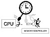 Figure
3.1 Moving data on the clock tick.
Figure
3.1 Moving data on the clock tick.
NOTE
In a DRAM setup—unsynchronized memory—only the CPU transmits and receives according to a clock tick. The memory controller has no idea a clock is ticking, and tries to send data back to the CPU, unaware of the swinging pendulum.
Synchronized DRAM (SDRAM)
Interruptions are known as Interrupt Requests (IRQs) and, to mix metaphors, they are like a two-year-old demanding attention. One way to handle them is to repeat "not now...not now...not now" until it's a good time to listen. Another way to handle an interruption is to say, "Come back in a minute and I'll be ready to respond then." The problem is explaining to the two-year-old what you mean by "a minute." We'll discuss IRQs in Chapter 4, "Processor Mechanics, IRQs, and DMA."
One day the boss had a great idea. There was a big clock in the front office (the motherboard oscillator) and he proposed that both he and the pressman wear a watch. That way, both of them could tell time. It was a novel idea: The boss would then be able to call out to the pressman that he had a job to run, and the pressman could holler back, "I'll be ready in a minute."
This could also work the other way around. When the pressman finished a job, he could call out to the boss that he was ready to deliver the goods. The boss could then shout back that he needed another minute because he was busy with a customer. Either one of them could watch the clock for a minute to go by, doing something else until the other one was ready to talk.
Another way to think of clock ticks is to imagine a ski lift. Regardless of whether anyone takes a seat, an endless chain goes up and down the slope. Each seat is a clock tick, and either the CPU or the memory controller can put a data bit on a seat. Synchronization is sort of like waiting until a seat comes by before putting a data bit on it. Asynchronous is something like trying to shove a data bit toward the ski lift without paying any attention at all to whether or not there's a seat nearby. Usually, the bit goes nowhere and the device has to try again, hoping a seat just happens to show up.
An interesting feature of SRAM is that it allows for timing and synchronization with the CPU. The same idea was retrofitted to DRAM chips, and synchronized memory was born. DRAM is called asynchronousbecause it reacts immediately and on its own, to any given instruction. SDRAM is synchronous because it waits for a clock tick before responding to instructions.
CAUTION
SDRAM provides a way for the memory controller and CPU to both understand clock ticks, and to adjust their actions according to the same clock.
Cycles and Frequencies
Any business can make more money by choosing different growth paths. One path is to move the product along faster. Speeding things up means that in a given time period, we can ship out more stuff (technical term). More stuff means more money, and the business grows. System performance is no different in a computer, and some improvements have come about by simply making things go faster.
Taking half as long to move a byte means moving twice as many bytes in a given time. If it takes 10 ticks to move one byte, then using 5 ticks to move the same byte means faster throughput. In other words, we can keep the byte the same size and move it in less time. This is essentially the underlying principle of multipliers and half ticks, and gave rise to double data rate (DDR) memory.
The power supply converts alternating current (AC) to direct current (DC), but that doesn't mean we never see alternating current again. Consider the oscillator, vibrating back and forth very quickly. How would that be possible, unless the associated electrical charges were moving back and forth? In fact, some components in a computer re-convert the incoming direct current to very low amperage alternating current. This isn't ordinary AC power, but means that small amounts of electricity reverse direction (polarity) for the purposes of timing and signaling.
Timing cycles are represented as waves moving up and down through a midpoint. The height between the top (peak) and bottom (trough) of a single wave cycle is called the amplitude. The number of waves being generated in a single second is called the frequency. We mentioned frequency in Chapter 2, in our discussion of bandwidth and broadband, but let's take a closer look at the specific concept.
Signal information moves at some frequency number. In Chapter 11, "Cables and Connectors," we reference various types of wire specifications, but as an example, Category 4 low-grade cable specifies a transmission rate of 20MHz. This means signals are passing through the wire at a cycle rate of twenty million waves per second. To produce both the timing of the cycles, and the characteristic up-reverse-down pattern of a wave, the electrical current must be moving in an alternating, cyclical flow pattern. (Think of your hand moving back and forth at one end of a tub of water. Although your arm is moving horizontally, the pulses of water are measured vertically.) The reversing directions of alternating current produce pulses of electricity that we see as waves on an oscilloscope.
Clock Speed and Megahertz
Clock speed is a frequency measurement, referring to cycles per second. It's usually written in megahertz (MHz), where "mega" refers to 1 million cycles per second and "giga" refers to one billion cycles per second. One cycle per second is 1Hz. The motherboard oscillator—a sort of electronic clock—is configured through jumpers to produce a specific frequency. Once again, the number of waves passing a given point in one second, from the start to finish of each wave, is the frequency of the cycle.
A single clock tick (wave cycle) is measured from the point where a wave begins to move upwards, all the way down and through a midline, to the point where the wave moves back up and touches the midline again. Figure
3.2 is a sine wave, with smooth up and down movements very similar to waves you see in water. Waves come in various shapes, but the two we'll be concerned with are the sine wave and the square or pulse wave. When you look at any signal wave on an oscilloscope, you'll see that the name refers to its actual shape.
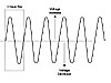 Figure
3.2 A sine wave.
Figure
3.2 A sine wave.
When you hear a sine wave generated on a synthesizer oscillator (not so different from a computer oscillator), it sounds very smooth, like a flute. The many steps taking place as the wave moves up and down make it an analog signal. We'll discuss the difference between analog and digital in Chapter 6, "Basic Electronics." A pulse wave, on the other hand, sounds very harsh, like a motorcycle engine. Pulse waves have three components we're interested in: the midline, the peak, and the trough. Figure
3.3 shows a pulse or square wave.
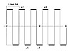 Figure
3.3 A square wave.
Figure
3.3 A square wave.
Note that in Figure 3.3, we've highlighted the top and bottom of the wave with a heavier, thicker line. The actual wave is the same signal strength, but we want you to see how a pulse wave is much like the on/off concept of any binary system. When we speak of the leading edge of a wave, we can also speak of the immediate-on, top of a pulse. Likewise, the trailing edge can be the immediate-on, bottom of the wave. The top is one polarity and can take on a +1 setting, whereas the bottom is the reversed polarity and can take on a -1 setting. When the wave is at the immediate-off centerline, it has a 0 setting.
Clock Multipliers
A computer timing oscillator is a piece of crystal. When it's connected to an electrical current, the crystal begins to vibrate, sending out very fast pulses of current. Pulses from the oscillator enter a frequency synthesizer, where the main frequency can be changed and directed to different components. The various fractional speeds are set with jumpers. Generally, the motherboard uses one fraction of the crystal's vibration, which constitutes the motherboard speed. The CPU uses a different fraction, usually faster than the motherboard.
NOTE
This is highly simplified for the purpose of creating an example only.
Suppose the crystal vibrates at 660MHz, and the motherboard speed is one twentieth of that: 33MHz (660/20). If the CPU uses one fifth of the crystal's frequency, it runs at 133MHz (660/5). That means the CPU is also running four times faster than the motherboard (33x4), making it a 4X processor.
The original XT machines used the same timing frequency for all the components on the motherboard. The 80486 introduced the concept of multipliers and frequency synthesizers. Nowadays, we see various frequencies being assigned to such things as the processor, the front-side bus, the memory bus, memory caches, the expansion bus, and so forth. The frequency assigned to the CPU's internal processing can also be sent to a high-speed L-1 cache.
TIP
When you hear that a memory controller is synchronized to a processor bus, it means a certain timing frequency is being derived from the main oscillator and "sent" to both devices.
Have you ever watched a group of children playing with a jump rope? Part of the game is to move the arc of the rope around a cylinder of space at some speed. At the high end of the arc, the rope passes over the jumper's head. At the low end of the arc, the jumper has to jump up and create a gap for the rope to pass between his feet and the ground. Each jump is like a 1-bit data transfer. The speed of the rope is the timing frequency.
Suppose we have two groups of children, where the pair on the left is twirling their rope in one direction. Their friends on the right are twirling a second rope, twice as fast, in the opposite direction. Let's not worry about the jumping kids, but instead, watch each rope in slow motion. Figure 3.4 shows the centers of each rope as they come close together. (Note that the following physics and math are incorrect, but we're using an example.)
The rope to the left, in Figure 3.4, is producing one cycle for every two cycles on the right. The CPU typically attaches a bit of information (represented by the cylinder on the rope) to each of its own cycles (the high end of the arc). Notice that a transfer to the memory controller takes place in one cycle, but the "rope" in the CPU passes by twice. For every two ticks taking place inside the CPU, the components working with the motherboard clock "hear" only a single tick. When the CPU attaches a bit to each wave (each turn of its rope), it has to wait until the memory cycle is ready for that second bit.
 Figure
3.4 Relative cycle speeds and one missed transfer.
Figure
3.4 Relative cycle speeds and one missed transfer.
We can improve performance in the CPU by adding a small buffer, or cache, to the motherboard, close to the CPU. When the processor and memory controller's timing cycles are synchronized, the processor can offload a bit directly to memory. When their cycles are out of sync, the CPU can still move its second bit into the buffer and get on with something else. Figure
3.5 shows how a small buffer (the little guy in the middle), synchronized to the processor, can temporarily store bits until the memory controller is ready for a transfer.
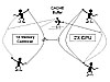 Figure
3.5 CPU transfers buffered to a "holding tank."
Figure
3.5 CPU transfers buffered to a "holding tank."
The small buffer we're talking about is the L-1 cache. In CPU-memory transfers, a buffer is the same as a cache. A critical difference is that memory caches do not work with probabilities. Each bit going into the cache is absolutely going to be sent to memory. When the L-1 cache fills up, the L-2 cache takes the overflow. If both the L-1 and L-2 buffers become filled, a Level 3 cache might be helpful. The goal is to ensure that bits are transferred for every single processor clock tick. Understand that the CPU can also recall bits from memory and use the caches. However, at twice the speed of memory, the CPU more often is ready, willing, and able to take bits while the memory controller is still searching.
To bring this together: Imagine installing a Pentium processor on a 66MHz motherboard, using a 4X clock multiplier. Internally, the Pentium moves data at 264MHz (call it 266Mhz). The memory controller runs at 66MHz (the speed of the motherboard). When the Pentium "hangs" a byte onto a clock tick, it may have to wait for up to four of its own cycles before the memory controller is ready to handle the transfer. This assumes we're using SDRAM and the controller "hears" the same ticks as the processor. Remember that DRAM had no timing link between the processor and CPU, and each component had to wait until the other wasn't busy before it could accomplish a transfer.
The PC100 Standard
Motherboard speeds eventually increased to 100MHz, and CPU speeds went beyond 500MHz. The industry decided that SDRAM modules should be synchronized at 100MHz. Someone had to set the standards for the way memory modules were clocked, so Intel developed the PC100 standard as part of the overall PCI standard. The initial standard made sure that a 100MHz module was really capable of, and really did run at 100MHz. Naturally, this created headaches for memory manufacturing companies, but the standard helped in determining system performance.
At 100MHz and higher, timing is absolutely critical, and everything from the length of the signal traces to the construction of the memory chips themselves is a factor. The shorter the distance the signal needs to travel, the faster it runs. Non-compliant modules—those that didn't meet the PC100 specification—could significantly reduce the performance and reliability of the system. The standard caught on, although unscrupulous vendors would sometimes label 100MHz memory chips as PC100 compliant. (This didn't necessarily do any harm, but it did leave people who built their own systems wondering why their computer didn't run as they expected.)
We evaluate memory speed partly on the basis of the actual memory chips in a module, and partly on the underlying printed circuit board and buses. Because of the physics of electricity, a module designed with individual parts running at 100MHz rarely reaches that overall speed. It takes time for the signals to move through the wire, and the wire itself can slow things down. This led to ratings problems similar to those involving processors, which are covered in Chapter 5.
PC66 Versus PC100
PC100 SDRAM modules required 8 ns DRAM chips, capable of operating at 125MHz. The extra twenty-five megahertz provides a margin of error, to make sure that the overall module will be able to run at 100MHz. The standard also called for a correctly programmed EEPROM, on a properly designed circuit board.
SDRAM modules prior to the PC100 standard used either 83MHz chips (12 ns) or 100MHz chips at 10 ns. They ran on systems using only a 66MHz bus. It happens that these slightly slower 100MHz chips could produce a module that would operate reliably at about 83MHz. These slower SDRAM modules are now called PC66, to differentiate them from the PC100 specification (with 8 ns chips).
As memory speeds increased, the PC100 standard was upgraded to keep pace with new modules. Intel released a PC133 specification, synchronized to a 133MHz chipset, and so it went. PC800 RDRAM was released to coincide with Intel's 800 series chipset, running at 800MHz. These days, we see a PC1066 specification, designed for even higher-speed memory. As bus speeds and module designs change, so too does the specification.
MHz to Nanosecond
SDRAM modules are rated in megahertz, so as to link the chip speed to the bus speed. To find the speed in nanoseconds, divide 1 second (1 billion nanoseconds) by the output frequency of the chip. For example, a 67MHz chip runs at 67-million cycles per second. If you divide one billion by 67 million, the result is 14.9, which rounds off to 15 ns.
You can use this same formula to make a loose comparison between processor speeds and memory modules. For example, we can take a 900MHz Pentium and divide one billion by 900 million. The result shows a CPU running at 0.9 nanoseconds. Compare a 12 ns SDRAM chip with this CPU and you can see how much faster the processor is running. Even when we take ultra-fast SRAM running at 2 ns, we can see a significant difference in speed. Understand that nanosecond timing numbers don't tell the whole story when it comes to performance.
NRZI and DDR
Instructions can be designed to begin from exact points in a wave cycle. This is another way of improving processor performance. When the cycle is going up, we refer to an "up tick." When the cycle is going down, we refer to a "down tick." Using an analog sine wave, we can use the midpoint for a 0 setting, and some amount of signal (other than zero) as a 1. This is the concept of Non-Return-to-Zero-Inverted (NRZI) encoding. NRZI encoding means that any variation in the voltage level produces a change in state. A steady voltage represents a 1, and any change at all in voltage represents a 0.
TIP
If we use a pulse wave, we can clearly differentiate between a zero, and two additional numbers: the +1 and the -1. Pipelining and double-data rate (DDR) memory both take advantage of the square design of a pulse wave to send two signals per clock tick.
Pipelining
Suppose your friend asks you to go buy a soda. Right as you turn to the door, he then asks you to hand him a pencil. Both instructions are mixed together, and you'll have to make a processing decision as to which takes priority. That decision moment slows down your overall actions. Essentially, when an asynchronous DRAM chip receives an instruction to store something, it runs into the same problem. It takes the first instruction, then processes it until it finishes. At that point, it "looks up," so to speak, to get another instruction.
On the other hand, when we're aware of our surroundings, someone can ask us to do something and also ask us to do something else when we're done. Although we're busy with the first task, we store the second task in a cache, knowing that as soon as we're finished with the first, we can begin the second. In other words, we don't have to be told a second time. This type of buffering (a very small memory cache) saves time for the person issuing the instructions.
Instead of being constantly interrupted, the clock and a pipeline cache in a memory module allows instructions to be organized one after the other. The process is called a pipeline system. Pipelining is a little like the way a CPU uses IRQ lines to make some sense out of the data stream chaos flying around in electronic space.
Using regular pipelining, a memory controller can write a bit to memory at the same time as it's "hearing" the next call from the CPU. Likewise, when it reads a bit from memory, it can have the next bit ready to go before the CPU asks for it. We'll encounter the concept of pipelining again when we take a look at Pentium processors in the next chapter. Dual-pipeline architecture means a chip can listen to a new instruction while it's completing the first instruction. This is yet another way to speed up any system or sub-system.
Pseudo Static RAM (PSRAM)
Synchronous DRAM takes into account interrupt timing and the motherboard clock, and works just like SRAM. Capacitors allow for higher density (and lower cost) of a DRAM chip, as opposed to the more expensive transistors on SRAM chips. Most SDRAM controllers are built into the North Bridge of the motherboard chipset.
Another type of memory is called Pseudo Static RAM (PSRAM). This is DRAM with built-in refresh and address-control circuitry to make it behave similarly to SRAM. It combines the high density of DRAM capacitors with the speed of SRAM, but instead of having to rely on the CPU for an accuracy check of the original "send," the built-in circuitry "remembers" the data correctly.
Larger Bytes and Wider Buses
The other way to improve performance is by increasing the size of the information packet (combining bytes) and moving everything at the original time. This is similar to increasing bus widths. For example, a piece of paper four inches wide and eight inches long can hold some number of words. Handing you a piece of paper still takes only one movement. But if the paper changes to eight inches wide, it can store a lot more words. In the same single movement, you receive much more information.
Summary—Basic Memory
We've seen that memory can be broadly divided into two categories: memory that the system can change, and that which the system cannot change. RAM and ROM, respectively, are the beginning concepts for understanding memory. The ROM BIOS is where the motherboard remembers the most basic instructions about the hardware of a particular chipset. CMOS stores system configuration settings, as well as settings for additional hardware connected to the basic chipset. BIOS and CMOS are different in that CMOS requires a small amount of electricity to maintain its settings.
BIOS and CMOS can be changed, but not without some effort. Make sure you know the acronyms associated with these chips and the ways in which they can be updated. Additionally, you should have a comfortable understanding about the following points having to do with memory:
- The central processing unit, the memory controller, and the system clock
- Clock cycles and multipliers, and how electrical data pulses are "pushed" along by clock pulses
- How timing affects performance, and the difference between asynchronous and synchronous data transfers
- The North Bridge and South Bridge architecture (see Chapter 2), and how the front side bus stands between the CPU and the North Bridge
We've talked about the original DRAM chips, and how they became SDRAM chips. The important change was when the memory controllers began to use timing frequencies to perform reads, writes, and refreshes. We've also examined the concept of timing oscillators and how their frequency can be divided into multipliers. Notice how we refer to the CPU speed as a multiple of slowest speed, and rarely as a fraction of a faster speed (a good marketing technique).
DRAM and SDRAM are both different from BIOS and CMOS. Be sure you know the acronyms, because you'll find them on the exam. SIMMs and DIMMs are modules, and we'll be discussing them shortly. Memory chips use different components as storage cells. After the chip has been manufactured, it's packaged onto a module. The individual chips fit onto a small IC board to form a module.
Cache Memory
Do you remember the printing business? Well, the company expanded, meaning there was more and more paperwork. Between print jobs, they had to send copies of financial statements and records off to the accounting department and the government. So the boss hired a secretary. At first, they sent these small jobs to the press room—after all, they were a printing company—but that was costing too much money. Finally, he bought a laser printer for himself (L-1 cache), and one for his secretary (L-2 cache) so they could do these quick little jobs themselves.
Whenever the boss was working up a price quote for a customer, he could set up various calculations and have his secretary print them off. Because they didn't have to go all the way to the press room (main memory), these temporary jobs were extremely quick. The CPU uses Level 1 and Level 2 caching in a similar fashion.
Level 1 (primary) cache memory is like the boss's own personal printer, right there by his desk. Level 2 (secondary) cache memory is like the secretary's printer in the next room. It takes a bit longer for the secretary to print a job and carry it back to the boss's office, but it's still much faster than having to run the job through the entire building.
CAUTION
Remember that the CPU uses memory caches to store data from registers that it will be using again soon. It also uses memory caches to store data on the way to memory, where the memory controller is too slow to capture each bit in relation to the CPU's timing speed. L-1 and L-2 caches run at the speed of the processor bus (also known as the front side bus). This allows the caches to capture a bit every time (clock tick) the processor sends a bit, or the reverse.
Memory Caches
Cache (pronounced "cash") is derived from the French word cacher, meaning to hide. Two types of caching are commonly used in personal computers: memory caching and disk caching. A memory cache (sometimes called a cache store, a memory buffer, or a RAM cache) is a portion of memory made up of high-speed static RAM (SRAM) instead of the slower and cheaper dynamic RAM (DRAM). Memory caching is effective because most programs access the same instructions over and over. By keeping as much of this information as possible in SRAM, the computer avoids having to access the slower DRAM.
The memory hierarchy is a way to handle differences in speed. "Hierarchy" is a fancy way of saying "the order of things; from top to bottom, fast to slow, or most important to least important." Going from fastest to slowest, the memory hierarchy is made up of registers, caches, main memory, and disks.
NOTE
When the processor needs information, it looks at the top of the hierarchy (the fastest memory). If the data is there, it wins. Otherwise, a so-called miss occurs, and the processor has to look in the next, lower level of hierarchy. When a miss occurs, the whole block of memory containing the requested missing information is brought in from a lower, slower hierarchical level. Some existing blocks or pages must be removed for a new one to be brought in.
Disk caching is different from memory caching, in that it uses a formula based on probabilities. If you are editing page one of a text you are probably going to request page two. So even if page two has not been requested, it is retrieved and placed in a disk cache on the assumption it will be required in the near future. Disk caches use main memory or in some cases additional memory included with the disk itself.
Memory caching is based on things the CPU has already used. When data or an instruction has been used once, the chances are very good the same instruction or data will be used again. Processing speed can be dramatically increased if the CPU can grab needed instructions or data from a high-speed memory cache rather than going to slower main memory or an even slower hard disk. The L1, L2, and L3 cache are made up of extremely high-speed memory and provide a place to store instructions and data that may be used again.
Using Memory Levels
Here's another way to understand the different levels of a hierarchy. Think of the answer to the following questions, and then watch what happens in your mind. What's your name? This information is immediately available to you from something like the ROM BIOS in a computer. What day is it? This information is somewhat less available and requires a quick calculation, or "remembering" process. This is vaguely like the CMOS settings in the system.
What's your address? Once again you have a fairly quick access to your long-term memory, and quickly call the information into RAM (your attention span). What's the address of the White House? Now, for the first time, you're likely to draw a blank. In that case you have two options: The first is that you might remember a particular murder-mystery movie and the title, which acts somewhat like an index pointer to retrieve "1600 Pennsylvania Avenue" from your internal hard drive. In other instances, you'll likely have to access process instructions, which point you to a research tool like the Internet or a phone book.
You should be able to see how it takes longer to retrieve something when you're less likely to use the information on a regular basis. Not only that, but an entire body of information can be stored in your mind, or you may have only a "stub." The stub then calls up a process by which you can load an entire application, which goes out and finds the information. If you expect to need something, you keep it handy, so to speak. A cache is a way of keeping information handy.
CAUTION
Understand that a cache is just a predefined place to store data. It can be fast or slow, large or small, and can be used in different ways.
L-1 and L-2 Cache Memory
The Intel 486 and early Pentium chips had a small, built-in, 16KB cache on the CPU called a Level 1 (L-1), or primary cache. Another cache is the Level 2 (L-2), or secondary cache. The L-2 cache was generally (not very often, anymore) a separate memory chip, one step slower than the L-1 cache in the memory hierarchy. L-2 cache almost always uses a dedicated memory bus, also known as a backside bus (see Figure 2.10 in Chapter 2).
A die, sometimes called the chip package, is essentially the foundation for a multitude of circuit traces making up a microprocessor. Today, we have internal caches (inside the CPU housing) and externalcaches (outside the die). When Intel came up with the idea of a small amount of cache memory (Level 1), engineers were able to fit it right on the die. The 80486 used this process and it worked very well. Then the designers decided that if one cache was good, two would be better. However, that secondary cache (Level 2) couldn't fit on the die, so the company had to purchase separate memory chips from someone else.
NOTE
Don't confuse a chip package with a chipset—the entire set of chips used on a motherboard to support a CPU.
These separate memory chips came pre-packaged from other companies, so Intel developed a small IC board to combine their own chips with the separate cache memory. They mounted the cards vertically, and changed the mounts from sockets to slots. It wasn't until later that evolving engineering techniques and smaller transistors allowed them to move the L-2 cache onto the die. In other words, not every design change is due to more efficient manufacturing.
CAUTION
For the purposes of the exam, you should remember that the primary (L-1) cache is internal to the processor chip itself, and the secondary (L-2) cache is almost always external. Modern systems may have the L-1 and L-2 cache combined in an integrated package, but the exam may easily differentiate an L-2 cache as being external. Up until the 486 family of chips, the CPU had no internal cache, so any external cache was designated as the "primary" memory cache. The 80486 introduced an 8KB internal L-1 cache, which was later increased to 16KB. The Pentium family added a 256KB or 512KB external, secondary L-2 cache.
Larger memory storage means more memory addresses, which, in turn, means larger numbers. A CPU register can store only a certain size byte, and larger numbers mean wider registers, as well as wider address buses. Note that registers (discussed again in Chapter 4) are usually designed around the number of bits a CPU can process simultaneously. A 16-bit processor usually has 16-bit registers; a 32-bit processor has 32-bit registers, and so forth. These larger numbers require a correspondingly wider data bus to move a complete address out of the processor.
TIP
You should be getting a sense of how larger and faster CPUs generate a chain of events that lead to whole new chipsets and motherboards. Not only does the chip run faster, but the internal registers grow larger, or new ways to move instructions more quickly demand faster bus speeds. Although we can always add cells to a memory chip, it isn't so easy to add registers to a microprocessor.
Larger numbers mean the memory controller takes more time to decode the addresses and to find stored information. Faster processing requires more efficient memory storage, faster memory chips, and better bus technology. Everything associated with timing, transfers, and interruptions must be upgraded to support the new central processor.
L-3 Caches
You may see references to an L-3—or a Level 3—cache. Tertiary (third) caches originated out of server technology, where high-end systems use more than a single processor. One way to add an L-3 cache is to build some additional memory chips directly into the North Bridge. Another way is to place the cache into a controller sub-system between the CPU and its dependent devices. These small I/O managers are part of hub architecture, discussed in Chapter 5. Newer Pentium 4 processors use up to 20-level pipelining operations; an L-3 cache would also be a way to offload next-due instructions from a memory controller.
Simply put: More and more CPUs have both the L-1 and L-2 cache built right onto the die. If a third cache remains outside the die, many people refer to it as a Level 3 cache. Level 3 caches are usually larger than L-2 caches, more often in the 1MB size range. All three types of cache usually run at the processor speed, rather than the speed of a slower memory bus. (Benchmark tests on single-processor systems have shown that an L-2 cache peaks out at about 512KB, so adding more memory to a third-level cache isn't always going to increase system performance.)
Memory Pages
The CPU sends data to memory in order to empty its registers and make room for more calculations. In other words, the CPU has some information it wants to get rid of, and sends that information out to the memory controller. The memory controller shoves it into whichever capacitors are available and keeps track of where it put everything. Each bit is assigned a memory address for as long as the controller is in charge of it (no pun intended).
When the CPU wants to empty a register, it waits for one of its internal electrical pulses (processor clock tick). When the pulse arrives, it sends out a data bit, usually to a memory cache. Very quickly, a stream of bits generates bytes in multiples of eight (8-bit byte, 16-bit bytes, and so on). The cache waits for the slower pulses of the motherboard clock, and then sends each bit over to the memory controller. The controller then directs each electrical charge into a memory cell. The cell might be a capacitor, in which case it has to be recharged. Or, it might be a transistor, in which case a switch opens or closes. Regardless of how wide a register or an address is, each bit ends up in its own cell, somewhere in the memory chip.
Page Ranges
Typically, memory is divided into blocks. At the main memory level, a block of memory is referred to as a memory page. A page is a related group of bytes (and their bits). It can vary in size from 512 bits to several kilobytes, depending on the way the operating system is set up. Understand that physical memory is fixed, with the amount of memory identified in the BIOS. However, the operating system dictates much of how the memory is being used. For example, a 32-bit operating system will structure memory pages in multiples of thirty-two bits; a 64-bit operating system will use pages that are multiples of sixty-four.
DRAM cells are usually accessed through paging. The controller keeps track of the electrical charges, their location, and the state (condition) of each capacitor and/or transistors of each memory chip. This combination of states and locations is the actual address.
Pages are similar to named ranges in a spreadsheet. Without ranges, a spreadsheet formula must include every necessary cell in a calculation. We might have a formula something like =SUM(A1+B1+C1+D1+E1). Now suppose we assign cells C1, D1, and E1 to a range, and call that range "LastWeek." We can now change the formula to include the range name: =SUM(A1+B1+"LastWeek"). The range name includes a set of cells.
A named range is analogous to the memory controller giving a unique name to part of a row of charges. This range of charges is called a page address. A memory page is some part of a row in a grid. A page address means that the controller doesn't have to go looking for every single capacitor or transistor containing particular data bits.
Do you remember that cheap little printing toy we talked about earlier—the one with the rubber letters and the rail? One way to think of memory addressing is as if we were trying to locate every single piece of rubber in the rail. The memory controller has to ask, "Get me letter 1, at the left end. Now get me letter 2, next to letter 1. Now get me letter 3, the third one in from the left," and so on. But suppose we don't worry about each letter, and think instead of the whole rail. Now the controller has only to ask, "Get me everything in the rail right now." This is more like memory paging.
Burst Mode
A burst of information is when a sub-system stores up pieces of information, and then sends them all out at once. Back in World War II, submarines were at risk every time they surfaced to send radio messages to headquarters. To reduce the time on the surface, people would record a message at a slow speed, and then play it back during the transmission in a single high-speed burst. To anyone listening, the message would sound like a quick stream of unintelligible noise.
"Bursting" is a rapid data-transfer technique that automatically generates a series of consecutive addresses every time the processor requests only a single address. In other words, although the processor is asking for only one address, bursting creates a block of more than that one. The assumption is that the additional addresses will be located adjacent to the previous data in the same row. Bursting can be applied both to read operations (from memory) and write operations (to memory).
On a system bus, burst mode is more like taking control of the phone line and not allowing anyone else to interrupt until the end of the conversation. However, memory systems use burst mode to mean something more like caching: The next-expected information is prepared before the CPU actually makes a request. Neither process is really a burst, but rather an uninterrupted transmission of information. Setting aside the semantics, burst mode takes place for only limited amounts of time, because otherwise no other sub-systems would be able to request an interruption.
Fast Page Mode (FPM)
Dynamic RAM originally began with Fast Page Mode (FPM), back in the late 1980s. Even now, many technical references refer to FPM DRAM or EDO memory (discussed next). In many situations, the CPU transfers data back and forth between memory, in bursts of consecutive addresses. Fast page mode simplifies the process by providing an automatic column counter. Keep in mind that addresses are held in a matrix, and that a given row is a page of memory. Each bit in the page also has a row-column number (address).
In plain DRAM, the controller not only had to find a row of bits (the page), it also had to go up and "manually" look at each column heading. Fast Page Mode automatically increments the column address, when the controller selects a memory page. It can then access the next cell without having to go get another column address. The controller uses fast page mode to make an assumption that the data read/write following a CPU request will be in the next three columns of the page row. This is somewhat like having a line of letters all ready to go in the toy stamp.
Using FPM, the controller doesn't have to waste time looking for a range address for at least three more times: It can read-assume-assume-assume. The three assumptions are burst cycles. The process saves time, and increases speed when reading or writing bursts of data.
NOTE
Fast Page Mode is capable of processing commands at up to 50 ns. Fifty nanoseconds is fifty billionths of a second, which used to be considered very fast. Remember that the controller first moves to a row, then to a column, then retrieves the information. The row and column number is a matrix address.
The Data Output Buffer
Suppose the CPU wants back 16 bits of data (two bytes). Figure 3.6 illustrates what happens next. Note that the controller has stored the data in what it calls Page 12, in the cell range 1–16. It passes through the memory chip, looking for Page 12, bit 1 (Cell A12). It then moves each bit into the data output buffer cell at the top of each column. Remember: The controller doesn't have to look again at the page number for bits number 2, 3, or 4. It's already read "page 12," and assumes-assumes-assumes. For the fifth bit, it quickly re-reads the page address, and then goes and gets bits 5, 6, 7, and 8. Notice that in two reads, the controller has picked up one byte: half of a 16-bit address.
After the controller completes its pass through the entire page (four reads: one complete number), it validates the information and hands it back to the CPU. The controller then turns off the data output buffer (above the columns, in Figure 3.6). This takes approximately 10 nanoseconds. Finally, each cell in the page is prepared for the next transmission from the CPU. The memory enters a 10 ns wait state while the capacitors are pre-charged for the next cycle. In other words, that part of the row is given a zero charge (wiped out) and prepared for the next transmission.
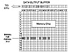 Figure
3.6 Memory controller retrieves cell data.
Figure
3.6 Memory controller retrieves cell data.
NOTE
Understand that FPM has a 20 ns wait state: 10 ns to turn off the data output buffer, plus 10 ns to recharge specific cells in a page.
Extended Data Output (EDO) RAM
FPM evolved into Extended Data Out (EDO) memory. The big improvement in EDO was that column cell addresses were merely deactivated, not wiped out. The data remained valid until the next call from the CPU. In other words, Fast Page Mode deactivated the data output buffer (10 ns), and then removed the data bits in the column cells (10 ns). EDO, on the other hand, kept the data output buffer active until the beginning of the next cycle, leaving the data bits alone. One less step means a faster process.
EDO memory is sometimes referred to as hyper-page mode, and allows a timing overlap between successive read/writes. Remember that the data output buffers aren't turned off when the memory controller finishes reading a page. Instead, the CPU (not the memory controller) determines the start of the deactivation process by sending a new request. The result of this overlap in the process is that EDO eliminates 10 ns per cycle delay of fast page mode, generating faster throughput.
Here's another way to look at it. When you delete a file, the operating system has two ways to go about the process. It can either write a series of zeroes over every bit of data pertaining to that file, everywhere they exist, or it can simply cancel the FAT index reference. Obviously it's a lot faster to just cancel the first letter of the file's index name than it is to spend time cleaning out every data bit. Utility software applications allow you to "undelete" a file by resetting the first letter of a recoverable file. These applications also provide a way to wipe out a disk by writing all zeros to the file area. In the latter case, nobody can recover the information. FPM is like writing all zeros to a disk, and EDO is like changing only the first letter of the index name.
Both FPM and EDO memory are asynchronous. (In the English language, the "a" in front of synchronous is called a prefix. The "a" prefix generally means "not," or "the opposite.") In asynchronous memory, the memory controller is not working with any other clocks. DRAM is asynchronous memory. In asynchronous mode, the CPU and memory controller have to wait for each other to be ready before they can transfer data.
Rambus Memory (RDRAM)
All the memory systems that we've talked about so far are known as wide channel systems because the memory channel is equal to the width of the processor bus. RDRAM is known as a narrow channelsystem because data is transferred only 2 bytes (16 bits) at a time. This might seem small, but those 2 bytes move extremely fast! The Rambus data bus is 16 bits wide, as opposed to the more typical 32 or 64 bits wide. Additionally, Rambus memory sends data more frequently. It reads data on both the rising and falling edges of the clock signal.
RDRAM
Rambus dynamic RAM comes out of technology developed originally by Rambus, Inc., for the Nintendo 64 gaming system. It's not that new, but it seems new because Intel started to use it with its Pentium 4 processors and 800-series chipset. Rambus memory is integrated onto Rambus Inline Memory Modules (RIMMs). The modules use Rambus DRAM (RDRAM) chips. We discuss memory modules (packaging) later in this chapter.
RDRAM chips use the processor's memory bus timing frequency, not the motherboard clock. Therefore, the processor won't request something at mid tick (the reverse of an interrupt). On the other hand, SRAM and SDRAM are synced to the CPU at a multiple closer to the motherboard clock. In other words, SDRAM, running at 100MHz, might be three times the speed of a 33MHz board.
RDRAM starts with the CPU speed, multiplied from a 66MHz board. A 10X processor on the same board would now be running at 660MHz. RDRAM then sets the memory bus to one half or one third of the CPU speed. 660 divided by two sets the memory bus at 330MHz. Divide by three, and the memory bus transfers at 220MHz. Both are faster than SDRAM. Remember that speed alone doesn't account for total performance.
Earlier Pentiums used a 64-bit bus and transferred data in parallel. The corresponding memory module bus was also 64 bits wide, which meant that data could be moved across the memory bus in 64-bit (8-byte) chunks. Another way of looking at it is that a bit is one-eighth of a byte. Therefore, 64 bits divided by 8 equals 8 bytes.
SLDRAM
Earlier memory chips used separate address, data, and control lines. This separation tended to limit speed. Engineers decided that joining the three types of data into a single packet and moving it across a single bus would improve efficiency. Along the way, they came up with two different methods, or protocols, for doing so. The protocol-based designs we'll mention are SyncLink DRAM (SLDRAM) and Rambus DRAM, sometimes called Direct Rambus DRAM (DRDRAM).
Intel eventually bought Rambus and began licensing the technology for a fee. SLDRAM, on the other hand, was an open industry standard. You may remember the problems IBM had with their micro-channel architecture buses. In the same way, memory manufacturers moved more toward SLDRAM. A secondary benefit of SLDRAM was that it doesn't require that existing RAM chips be redesigned. RDRAM, with its narrow channel bus, is a whole new architecture.
The original SLDRAM used a 200Mhz bus, making it faster than standard SDRAM. Double Data Rate SDRAM (DDR SDRAM) and SLDRAM both use the rising and falling edge of the clock to move twice the amount of information as SDRAM. As such, the overall transfer started out at 400MHz and quickly moved up to 800MHz.
Prior to Rambus memory, the fastest chips had a throughput of 100MHz. SDRAM with a 64-bit bus (to match the Pentium) transfers data in 8-byte chunks. Eight megabytes moving in parallel means an 8MB transfer every second. RDRAM chips transfer data in 2-byte chunks, twice per cycle (one on the up tick, one on the down tick). At 800MHz, RIMMs move 1,600MB per second (2 transfers per cycle times 800), which translates to 1.66 gigabytes (GB) or a billion bytes—about twice as fast as SDRAM.
Double Data Rate SDRAM (DDR SDRAM)
SLDRAM generated DDR SDRAM and DDR-II. Both use a newer version of the Intel i845E chipset. Double Data Rate (DDR) came about as a response to Intel's RDRAM changed architecture and licensing fees. AMD was developing faster processing by using a double-speed bus. Instead of using a full clock tick to run an event, they used a "half-tick" cycle, which is the voltage change during a clock cycle. As the clock begins a tick, the voltage goes up (an up tick) and an event takes place. When the clock ends the tick, the voltage goes down (a down tick) and a second event takes place. Every clock cycle has two memory cycle events. The AMD Athlon and Duron use the DDR specification with the double-speed bus.
DDR and Rambus memory are not backward compatible with SDRAM. The big difference between DDR and SDRAM memory is that DDR reads data on both the rising and falling edges of the clock tick. SDRAM only carries information on the rising edge of a signal. Basically, this allows the DDR module to transfer twice as much data as SDRAM in the same time period. For example, instead of a data rate of 133MB/s, DDR memory transfers data at 266MB/s.
DDR is packaged in dual inline memory modules (DIMMs) like their SDRAM predecessors. They connect to the motherboard in a similar way as SDRAM. DDR memory supports both ECC (error correction code, typically used in servers) and non-parity (used on desktops/laptops). We discuss parity at the end of this chapter.
NOTE
RDRAM also developed a different type of chip packaging called Fine Pitch Ball Grid Array (FPBGA). Rambus chips are much larger than SDRAM or DDR die, which means that fewer parts can be produced on a wafer. Most DDR SDRAM uses a Thin Small Outline Package (TSOP). TSOP chips have fairly long contact pins on each side. FPBGA chips have tiny ball contacts on the underside. The very small soldered balls have a much lower capacitive load than the TSOP pins. DDR SDRAM using FPBGA packaging runs at 200–266MHz, whereas the same chips in a TSOP package are limited to 150–180MHz.
DDR-II
The current PC1066 RDRAM can reach 667MHz speeds (which is really PC1333), so Samsung and Elpida have announced that they are studying 1,333MHz RDRAM and 800MHz memory (PC1600). These systems would most likely be used in high-end network systems, but that doesn't mean that RDRAM would be completely removed from the home consumer market. Rambus has already developed a new technology, codenamed "Yellowstone," which should lead to 3.2GHz memory, with a 12.4GB/s throughput. With a 128-bit interface, Rambus promises to achieve 100GB/s throughput. Yellowstone technology is expected to arrive in game boxes first, with PC memory scheduled for sometime around 2005.
DDR-II may be the end of Rambus memory, although people have previously speculated that RDRAM wouldn't last. DDR-II extends the original DDR concept, taking on some of the advantages developed by Rambus. DDR-II uses FPBGA packaging for faster connection to the system, and reduces some of the signal reflection problems (collisions) of the original DDR. However, latency problems increase with higher bus speeds. DDR-II is entering the consumer market, but RDRAM is expected to continue, although with limited chipset support.
Serial Transfers and Latency
One of the problems with Rambus memory is that the RIMMs are connected to the bus in a series. A data item has to pass through all the other modules before it reaches the memory bus. The signal has to travel a lot farther than it does on a DIMM, where the bus uses parallel transfers. The longer distance introduces a time lag, called latency. The longer the delay before the signal reaches the bus, the higher the latency. In a Nintendo game, data generally moves in long streams, so serial transfers aren't a problem. But in a typical PC, data routinely moves in short bursts, and latency becomes a problem.
To understand latency, take a look at the difference between serial and parallel transfers. Think of a train in a movie scene. The hero is at one end of the train and has to chase the bad guy, using a serial process. He goes from one end of a car, along all the seats, and then leaves by a door at the other end, which is connected to the next car in the train. Then the process starts all over again, until he either reaches the end of the train or someone gets killed.
Now take that same train, but this time there isn't a hero chasing a bad guy. Instead, imagine a train full of people on their way to work. If there was only one door at the back of the train, it would take forever to let everyone off at the train station. To fix that problem, each car has its own door. When the train comes to a stop, everyone turns to the side facing the platform: The doors in each car open up, and people leave each car simultaneously. This is a parallel transfer.
RDRAM uses a 16-bit bus for the data signals. This narrow 2-byte path is the main reason why RDRAM can run at higher speeds than SDRAM. Keep in mind that transfers are not only faster, but there are two of them per cycle. On the other hand, one of the problems with parallel transfers at high speeds is something called skew. The longer and faster the bus gets, the more likely it is that some data signals will arrive too soon or too late: not in a perfect line. It would be as if sixty-four people started to leave the train at the same time, but each one stepped onto the platform at a different time.
SLDRAM uses a lower clock speed, which reduces signal problems. With no licensing fees, it's also cheaper to produce. Another useful feature is that it has a higher bandwidth than DRDRAM, allowing for a potential transfer of 3.2GB/s, as opposed to Rambus's 1.6GB/s. (Note that modern Intel chipsets use two parallel Rambus channels to reach 3.2GB/s.)
NOTE
Intel went the Rambus course, and released the 800 series chipset to work only with RDRAM. Soon after, Via released a chipset that would run DDR memory, an outgrowth of the SLDRAM technology. AMD wasn't going to be limited to an Intel board, so much of the market jumped on the Via chipset. This put pressure on Intel to come up with a modified 840-series chipset that would also support DDR memory. It appears as though Rambus may have a hard battle to win market share, but it continues to hang on in high-end desktops and workstations.
In a nutshell, fast and long may not be the same as slow and short. For instance, suppose you want to go two miles to the store. If you go the long way, using a highway, it's a ten-mile drive. However, you can drive 60 mph on the highway. If you go directly to the store, you're stuck driving 30 mph on local roads. Using the highway, you arrive in six minutes (60 mph/10 miles). The other way, you arrive in four minutes (30 mph/2 miles). You might drive a whole lot faster on the highway, but you'll get to the store faster on the straight-line route. In this example, the store is the memory controller. The different roads represent different types of bus architectures.
Video RAM (VRAM)
VRAM (Video RAM) and WRAM (Windows RAM) have been mostly supplanted by DDR memory chips, but you may find a question about VRAM (pronounced "vee-ram") on the exam. Video RAM was designed to provide two access paths to the same memory address. It's as if VRAM were a café that has two doors: one in the front and one in the back. Information comes in one "entrance" at the same time that other information flows out the other "exit." When the video controller reads the memory for information, it accesses an address with one of the paths. When the CPU writes data to that memory, it accesses the address via the other path. Because of these two access paths, we say that VRAM is dual-ported.
Manipulating graphics is processing-intensive, and so this capability to push data in and out of the chip at the same time helps a moving image appear continuous. In a way, the concept is similar to pipelining, but dual-porting uses one channel for "in" and the other channel for "out." Pipelining uses only one channel, but doesn't have to ask for instructions twice. VRAM chips are about 20% larger than DRAM chips because of extra circuitry requirements. (Modern computers usually have basic graphics processing integrated right onto the motherboard, with the AGP providing for faster video processing.)
VRAM, WRAM, and AGP
The AGP acronym stands for Accelerated Graphics Port. Most computers include this accelerated port, which is an integrated part of the I/O system. An AGP is not the same thing as VRAM or a video accelerator card, nor is it the same thing as today's integrated graphics. Although some video cards still use the main expansion bus, most connect with the AGP.
To say that a computer has "AGP memory" or "comes with AGP" can be confusing at best. At worst, it can demonstrate a faulty knowledge of the distinction between video memory and I/O subsystems. AGP is discussed in the "Accelerated Graphics Port (AGP)" section of Chapter 9, "Peripherals: Output Devices."
WRAM is short for Windows RAM, and has no connection with Microsoft, even though the acronym includes the word "Windows." WRAM, like VRAM, is dual-ported, but uses large block addressing to achieve higher bandwidth. Additional features provided better performance than video RAM at lower manufacturing costs. With the advent of AGP and DDR memory, both VRAM and Windows RAM have faded from the marketplace. That's not to say that add-on graphics accelerator cards have vanished.
Supplemental Information
VRAM has been superseded by DDR SDRAM and Synchronous Graphics RAM (SGRAM). This is a specialized form of SDRAM that uses bit masking (writing to a specified bit plane without affecting the others) and block writes (filling a block of memory with a single color). Synchronous Graphics RAM uses very fast memory transfers. It also incorporates specific design changes for certain acceleration features built into video cards. SGRAM is still single-ported, unlike VRAM or WRAM, but offers performance similar to VRAM. SGRAM is typically used in moderate to high-end cards where performance is important, but very high resolution isn't required.
Multibank DRAM (MDRAM)
Multibank DRAM was invented by MoSys, specifically for use in graphics cards, and differs substantially in design from other types of video memory. Conventional memory designs use a single block of memory for the frame buffer. MDRAM breaks its memory up into multiple 32KB banks that can be accessed independently. This means that instead of the entire bandwidth being devoted to a single frame, smaller pieces can be processed in an overlapped system. This overlapping is called interleaving, and isn't the same as interlaced monitors, which we discuss in Chapter 9.
Given that other forms of video memory use these single blocks, video cards tend to be manufactured with increments of whole megabytes of memory, typically in 1MB, 2MB, 4MB, or 8MB, and so forth. A monitor running 1,024x768 resolution in true color (24 bits) uses 2.25MB of video memory for the frame buffer. That's more than 2MB, but the next step up is 4MB, leaving 1.75MB of wasted memory. MDRAM has no such restriction, allowing video cards to be manufactured with any amount of RAM, even exactly 2.25MB.
Earlier, we mentioned that VRAM and WRAM are dual-ported. Table 3.2 lists the various types of memory, along with the way they're ported. You probably won't need to know single or dual, but this may help put all the types of memory in one place.
Table 3.2 Types of Memory Used for Video Processing
Memory Type
|
Ports
|
Standard (FPM) DRAM
|
Single
|
EDO DRAM
|
Single
|
VRAM
|
Dual
|
WRAM
|
Dual
|
SGRAM
|
Single
|
MDRAM
|
Single
|
Packaging Modules
We've discussed how memory chips work on the inside, but you'll need to know how these chips are installed on a motherboard. Most of the changes in form came about either to make maintenance easier or to avoid bad connections. Keep in mind that installing a combined unit or module of some kind is less expensive than having many individual units to install. (This is one reason why Intel wanted to get the Level 2 cache onto the die, rather than onto a separate processor IC board.)
Everything about the packaging of memory chips rests on the concept of modules. These modules are vaguely like tiny motherboards within a motherboard, in that they, too, are integrated circuit boards. The big difference between DRAM and SDRAM is the synchronization feature. Be sure you understand how SDRAM uses timing cycles to more efficiently interrupt the CPU. Remember, SRAM is extremely fast and is used in secondary caches; SDRAM is a type of main memory.
It's all well and good to know how SDRAM differs from Rambus RAM, but you're also going to have to be able to differentiate between SIMMs and DIMMs. Inline memory modules are the small IC cards you install in your machine when you upgrade your memory. You won't have to remember clock speeds and the exact number of pins, but you'll definitely be tested on the different types of modules. (That being said, keep in mind that SIMMs are usually 30-pin or 72-pin modules, and DIMMs often use a 168-pin configuration.)
Dual Inline Package (DIP)
Originally, DRAM came in individual chips called dual inline packages (DIPs). XT and AT systems had 36 sockets on the motherboard, each with one DIP per socket. Later, a number of DIPs were mounted on a memory board that plugged into an expansion slot. It was very time consuming to change memory, and there were problems with chip creep (thermal cycling), where the chips would work their way out of the sockets as the PC turned on and off. Heat expanded and contracted the sockets, and you'd have to push the chips back in with your fingers.
To solve this problem, manufacturers finally soldered the first 640 kilobytes of memory right onto the board. Then the problem was trying to replace a bad chip. Finally, chips went onto their own card, called a single inline memory module or SIMM. On a SIMM, each individual chip is soldered onto a small circuit board with an edge connector. Prices had fallen, so it was cost effective to simply replace the whole module if a memory chip failed.
Connectors: Gold Versus Tin
SIMMs and DIMMs come with either tin (silver-colored) or gold edge connectors. Although you may assume that gold is always better, that's not true. You'll want to match the metal of the edge connectors to the metal in the board's socket. If the motherboard uses gold sockets, use a gold SIMM. Tin sockets (or slots) should use tin edge connectors. The cost difference is minimal, but matching the metal type is critical.
Although it's true that gold won't corrode, a gold SIMM in a tin connector will produce much faster corrosion in the tin connectors. This quickly leads to random glitches and problems, so look at the board and match the color of the metal.
It's important to note, too, that each module is rated for the number of installations, or insertions. Each insertion causes scratches, and the more metal that is scratched off, the worse the connection becomes. In flea market exchanges and corporate environments, modules are subjected to constant wear and tear, and nobody is looking at the rated number of insertions.
Single Inline Memory Modules (SIMMs)
When DRAM chips were placed in a line on their own circuit board, it gave rise to the term inlinememory. After the chips were formed into a module, the entire module would fit into a socket on the board. These modules and sockets are referred to as memory banks. Depending on how the chips are connected on their own little circuit board, the module is called either a single or dual inline memory module (SIMM or DIMM).
CAUTION
Remember that SIMM, with an S, is a Single inline memory module. D is for double, and DIMM is a dual (two) inline memory module, with connectors on two sides, making it a double-edged connector. DIP is a dual inline package, but refers to single chips.
SIMMs come in both 30-pin and 72-pin versions. The 30-pin module is an 8-bit chip, with 1 optional parity bit. The 72-pin SIMM is a 32-bit chip, with 4 optional parity bits.
The memory bus grew from 8 bits to 16 bits, and then from 32 bits to 64 bits wide. The 32-bit bus coincided with the development of the SIMM, which meant that the 32-bit-wide data bus could connect directly to one SIMM (4 sets of 8 bits). However, when the bus widened to 64 bits, rather than making a gigantic SIMM, boards started using two SIMMs in paired memory banks. The 64-bit-wide DIMM was developed after the SIMMs, and went back to using only one module per socket again.
CAUTION
SIMMs and DIMMs are sometimes referred to as chips, but they are really series of chips (modules). DRAM itself is a chip, and many chips are grouped together to form SIMMs and DIMMs. SIMMs can come with a varying number of pins, including 30-pin and 72-pin. (Even though the 72-pin module could have chips on both sides, it was still a SIMM.)
Be careful when you read a question on the exam that you don't accidentally agree that a SIMM is a memory chip. A good way to keep alert is that chips have RAM in their name: DRAM, SRAM, SDRAM, RDRAM, and so forth.
Dual Inline Memory Modules (DIMMs)
Dual inline memory modules are very similar to SIMMs in that they install vertically into sockets on the system board. DIMMs are also a line of DRAM chips, combined on a circuit board. The main difference is that a dual module has two different signal pins, one on each side of the module. This is why they are dual inline modules.
The differences between SIMMs and DIMMs are as follows:
- A DIMM has opposing pins on either side of its board. The pins remain electrically isolated to form two separate contacts—a dual set of electrical contacts (sort of like a parallel circuit).
- A SIMM also has opposing pins on either side of the board. However, the pins are connected, tying them together. The connection forms a single electrical contact (sort of like a series circuit).
DIMMs began to be used in computers that supported a 64-bit or wider memory bus. Pentium MMX, Pentium Pro, and Pentium II boards use 168-pin modules. They are 1 inch longer than 72-pin SIMMs, with a secondary keying notch so they'll fit into their slots only one way.
Don't Mix Different Types of Memory
Mixing different types of SIMMs or DIMMs within the same memory bank prevents the CPU from accurately detecting how much memory it has. In this case, the system will either fail to boot, or will boot and fail to recognize or use some of the memory.
- You can, however, substitute a SIMM with a different speed within the same memory bank, but only if the replacement is equal to or faster than the replaced module.
- All memory taken together (from all memory banks) will be set to the speed of the slowest SIMM.
Rambus Inline Memory Modules (RIMMs)
Rambus inline memory modules (RIMMs) use Rambus memory chips. On a standard bi-directional bus, prior to Rambus memory, data traveled down the bus in one direction, with returning data moving back up the same bus in the opposite direction. This same process took place for each bank of memory, with each module being addressed separately. As a result, the system entered a wait state until the bus was ready for either type of transfer.
RIMMs use a looped system, where everything is going in one direction (uni-directional) all the time. In a looped system, data moves forward from chip to chip and module to module. Data goes down the line, and then the results data continues forward on the wire in the same direction. The results data doesn't have to wait for downstream data to finish being sent.
Continuity Modules
Because Rambus memory works with serial transfers, there must be a memory module in every motherboard memory slot. Even if all the memory is contained in a single module, the unused sockets must have an installed printed circuit board, known as a continuity module, to complete the circuit. This is similar to a string of lights, wired in series, where every socket requires a bulb.
RDRAM chips are set on their modules contiguously (next to each other in a chain) and are connected to each other in a series. This means that if an empty memory bank socket is in between two RIMM chips, you must install a continuity module. These are low-cost circuit boards that look like a RIMM, but with no memory chips. All the continuity module does is allow the current to move through the chain of RDRAM chips.
NOTE
RDRAM is fast for two reasons: It doesn't have to wait for the bus to turn around, and the cycle time is running at a fast 800MHz, so it doesn't have to wait very long for the next cycle. Using RDRAM chips, signals go from one module to the next to the next, and the throughput is triple that of 100MHz SDRAM. There can also be four RDRAM channels (narrow channel memory) at the same time. This can increase throughput to either 3.2GB (dual channel) or 6.4GB (all four channels).
Memory Diagnostics—Parity
The first thing a PC tests when it runs through the POST (Power On Self-Test) is the memory integrity. On many machines we can see this taking place as a rapidly increasing number displayed on the monitor before anything else happens. The testing is designed to verify the structural fitness of each cell (usually capacitors) in every main memory module. When all the cells have been checked, the boot process continues. The POST test is a simple, one-time test, and may not uncover a bad memory module.
NOTE
A bad memory module can cause strange, intermittent errors having to do with read failures, page faults, or even more obscure error messages. Before you tear apart Windows in an attempt to diagnose a possible operating system problem, run a comprehensive hardware diagnostics program on the machine. These applications do a much more exhaustive test of each memory cell, and produce a report of a failed module by its location in the memory banks.
Memory modules may or may not use parity checking, depending on how they're manufactured. The circuitry must be built into the module for it to be capable of parity checking. Keep in mind that parity checking is not the same as the initial test of the cells. Parity checking takes place only after the machine is up and running, and is used to check read/write operations.
Originally, parity checking was a major development in data protection. At the time, memory chips were nowhere near as reliable as they are today, and the process went a long way toward keeping data accurate. Parity checking is still the most common (and least expensive) way to check whether a memory cell can accurately hold data. A more sophisticated (and expensive) method uses Error Correcting Code (ECC) parity.
NOTE
Most DRAM chips in SIMMs or DIMMs require a parity bit because memory can be corrupted even if the computer hasn't actually been bashed with a hammer. Alpha particles can disturb memory cells with ionizing radiation, resulting in lost data. Electromagnetic interference (EMI) also can change stored information.
Even or Odd Parity
In odd and even parity, every byte gets 1 parity bit attached, making a combined 9-bit byte. Therefore, a 16-bit byte has 2 parity bits, a 32-bit byte has 4 parity bits, and so forth. This produces extra pins on the memory module, and this is one of the reasons why various DIMMs and SIMMs have a different number of pins.
Again, parity adds 1 bit to every 8-bit byte going into memory. If parity is set to odd, the circuit totals the number of binary "1s" in the byte and then adds a 1 or a 0 in the ninth place to make the total odd. When the same byte is read from memory, the circuit totals up all eight bits to ensure the total is still odd. If the total has changed to even, an error has occurred and a parity error message is generated. Figure
3.7 shows various bytes of data with their additional parity bit.
Even parity checking is where the total of all the 1 bits in a byte must equal an even number. If five of the bits are set to 1, the parity bit will also be set to 1 to total six (an even number). If 6 bits were set to 1, the parity bit would be set to 0 to maintain the even number six.
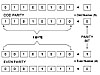 Figure
3.7 Odd and even parity.
Figure
3.7 Odd and even parity.
Fake or Disabled Parity
Some computer manufacturers install a less expensive "fake" parity chip that simply sends a 1 or a 0 to the parity circuit to supply parity on the basis of which parity state is expected. Regardless of whether the parity is valid, the computer is fooled into thinking that everything is valid. This method means no connection whatsoever exists between the parity bit being sent and the associated byte of data.
A more common way for manufacturers to reduce the cost of SIMMs is to simply disable the parity completely, or to build a computer without any parity checking capability installed. Some of today's PCs are being shipped this way, and they make no reference to the disabled or missing parity. The purchaser must ensure that the SIMMs have parity capabilities, and must configure the motherboard to turn parity on.
Error Correction Code (ECC)
Parity checking is limited in the sense that it can only detect an error—it can't repair or correct the error. The circuit can't tell which one of the eight bits is invalid. Additionally, if multiple bits are wrong but the result according to the parity is correct, the circuit passes the invalid data as okay.
CAUTION
You'll receive a parity error if the parity is odd and the circuit gets an even number, or if the parity is even and the parity circuit gets an odd number. The circuit can't correct the error, but it can detect that the data is wrong.
Error correction code (ECC) uses a special algorithm to work with the memory controller, adding error correction code bits to data bytes when they're sent to memory. When the CPU calls for data, the memory controller decodes the error correction bits and determines the validity of its attached data. Depending on the system, a 32-bit word (4 bytes) might use four bits for the overall accuracy test, and another two bits for specific errors. This example uses 6 ECC bits, but there may be more.
ECC requires more bits for each byte, but the benefit is that it can correct single-bit errors, rather than only the entire word. (We discuss bytes and words in the next chapter.) Because approximately 90% of data errors are single-bit errors, ECC does a very good job. On the other hand, ECC costs a lot more, because of the additional number of bits.
CAUTION
Remember that ECC can correct single-bit errors. However, like odd-even parity, it can also detect (not correct) multi-bit errors. Regular parity checking understands only that the overall byte coming out of memory doesn't match what was sent into memory: It cannot correct anything.
Usually, whoever is buying the computer decides which type of data integrity checking he or she wants, depending mainly on cost benefits. The buyer can choose ECC, parity checking, or nothing. High-end computers (file servers, for example) typically use an ECC-capable memory controller. Midrange desktop business computers typically are configured with parity checking. Low-cost home computers often have non-parity memory (no parity checking or "fake" parity).
XXX . XXX 4%zero null 0 1 2 3 4 Charging up random access memory
Random access memory (RAM) device architecture using ferroelectric tunneling RAM
The demonstrated room temperature ferroelectric states in ultra-thin films of tin and tellurium and have filed a provisional patent for a new kind of random access memory that they call ferroelectric tunneling random access memory. Experiments showed that memory could be written through a top gate voltage, which “flips” the in-plane polarization of the ferroelectric film, and read by a voltage tunneling through an edge without erasing the memory state.
Just as magnetic materials have opposing North and South poles, ferroelectric materials have opposing positive charges and negative charges that exhibit measurable differences in electric potential. demonstrated this ferroelectric behavior along the edges of atomically thin tin-tellurium film at room temperature.
Measurements showed the energy gap, or bandgap, of this ultra-thin (2-D) film to be about eight times higher than the bandgap in bulk (3-D) tin-tellurium, with an on/off ratio as high as 3,000, they report July 15 in the journal Science. Their findings hold promise for making random access memory (RAM) devices from this special semiconductor material, which is known as a topological crystalline insulator.
“This discovery is very exciting because usually when you decrease the thickness from the 3-D to 2-D, the phase transition temperature always decreases and therefore could destroy the ferroelectricity. But in this case, the [ferroelectric] phase transition temperature increased. It’s quite unusual,”
A unit cell is the smallest repeating pattern of atoms in the tin-tellurium molecular structure. Built on a base of graphene and silicon carbide, the tin-tellurium layers in the experiments ranged in size from 1 to 8 unit cells. In an actual device, the tin-tellurium would be capped with insulating material, as seen in the illustration in the slideshow above. The new study shows this ferroelectric state persists up to only about 26 F in the single-unit cell thin film tin-tellurium material, but in 2-, 3- and 4-unit cells, the ferroelectric state was robust to 300 kelvins, or 80 F, the highest temperature the experimental apparatus could measure.
“Room-temperature devices could have a very large commercial application. That’s why we are very excited about this work; it’s really robust even in room temperature .
Tests showed that memory could be written through a top gate voltage, which “flips” the in-plane polarization of the ferroelectric film, and read by a voltage tunneling through an edge without erasing the memory state. Evidence of this behavior in a sample that was a mere 16-nanometers in width means that tin-tellurium memory cells could be densely packed. Nanosensors and electronics are also possible.
Zeros and ones
Advantages of ferroelectric memory include lower-power consumption, fast write operations, and durable storage, Liu says. The MIT-Tsinghua results show the separation of positive and negative charges, or polarization, in their sample was in-plane, or parallel, with the atomically flat sample, creating a potential change on the edges of square-shaped islands of the material. Since this potential difference along edges is measurably different, one with large tunneling current, the other small, it can realize two different states that represent either a zero or a one, and these states can be detected simply by measuring the current.
“Based on this property, we proposed a new kind of random access memory. We call it ferroelectric tunneling random access memory, who proposed the initial architecture for this kind of memory, the protection and is in the process of filing a utility covering the findings regarding in-plane polarization and tunneling current. “It’s very simple, and it’s really practical,
Mathematical calculations known as density functional theory matched the experimental findings that there are 1/20 to 1/30 as many tin vacancies in the atomically thin tin-tellurium film than in the bulk form of the material. This lack of defects is believed to contribute to formation of the ferroelectric state.
The next step will be to show these results in actual devices. Future challenges include how to easily and inexpensively produce high quality tin-tellurium thin films and how to precisely control the polarization direction.
The next step will be to show these results in actual devices. Future challenges include how to easily and inexpensively produce high quality tin-tellurium thin films and how to precisely control the polarization direction.
XXX . XXX 4%zero null 0 1 2 3 4 5 6 Eye Movement Monitoring of Memory
Explicit (often verbal) reports are typically used to investigate memory (e.g. "Tell me what you remember about the person you saw at the bank yesterday."), however such reports can often be unreliable or sensitive to response bias 1, and may be unobtainable in some participant populations. Furthermore, explicit reports only reveal when information has reached consciousness and cannot comment on when memories were accessed during processing, regardless of whether the information is subsequently accessed in a conscious manner. Eye movement monitoring (eye tracking) provides a tool by which memory can be probed without asking participants to comment on the contents of their memories, and access of such memories can be revealed on-line 2,3. Video-based eye trackers (either head-mounted or remote) use a system of cameras and infrared markers to examine the pupil and corneal reflection in each eye as the participant views a display monitor. For head-mounted eye trackers, infrared markers are also used to determine head position to allow for head movement and more precise localization of eye position. Here, we demonstrate the use of a head-mounted eye tracking system to investigate memory performance in neurologically-intact and neurologically-impaired adults. Eye movement monitoring procedures begin with the placement of the eye tracker on the participant, and setup of the head and eye cameras. Calibration and validation procedures are conducted to ensure accuracy of eye position recording. Real-time recordings of X,Y-coordinate positions on the display monitor are then converted and used to describe periods of time in which the eye is static (i.e. fixations) versus in motion (i.e., saccades). Fixations and saccades are time-locked with respect to the onset/offset of a visual display or another external event (e.g. button press). Experimental manipulations are constructed to examine how and when patterns of fixations and saccades are altered through different types of prior experience. The influence of memory is revealed in the extent to which scanning patterns to new images differ from scanning patterns to images that have been previously studied 2, 4-5. Memory can also be interrogated for its specificity; for instance, eye movement patterns that differ between an identical and an altered version of a previously studied image reveal the storage of the altered detail in memory 2-3, 6-8. These indices of memory can be compared across participant populations, thereby providing a powerful tool by which to examine the organization of memory in healthy individuals, and the specific changes that occur to memory with neurological insult or decline 2-3, 8-10
Protocol
Equipment used during data acquisition
Eye tracker
The eye tracker used in the current protocol is an EyeLink II system (SR Research Ltd; Mississauga, Ontario, Canada). This head-mounted, video-based eye tracker records eye position in X, Y-coordinate frame at a sampling rate of either 500 or 250 Hz, with a spatial resolution of < 0.1°. One camera is used to monitor head position by sending infrared markers to sensors placed on the four corners of the display monitor that is viewed by the participants. Two additional cameras are mounted on the headband situated below each of the eyes, and infrared illuminators are used to note the pupil and corneal reflections. Eye position may be based on pupil and corneal reflections, or based on the pupil only. The padded headband of the eye tracker can be adjusted in two planes to comfortably fit the head size of an adult participant. Most eyeglasses and contact lenses can be accommodated by the eye tracker.
Computers
Two PCs are used to support eye movement recording. One computer serves as the display computer, which presents the calibration screens, necessary task instructions and the images used in the experimental paradigm to the participants. The display computer details the data collection parameters that are then governed by the second, host computer. The host computer calculates real-time gaze position and records the eye movement data for later analysis, as well as any button press or keyboard responses made the participant. Participant setup and operations of the eye tracker are performed via the host PC.
Software
In this protocol, the timing and order by which experimental stimuli are to be presented to the participants, and the manner in which eye position is to be collected by the host PC are programmed through Experiment Builder, a software program specifically developed by SR Research Ltd to interface with the eye tracker host computer. However, stimulus presentation can also be conducted through other software programs (e.g., Presentation, Neurobehavioral Systems; Albany, CA). Conversion of the eye movement data to a series of fixation and saccade events that are time-locked to stimulus presentation (or another external event) is achieved through the host computer and can be interrogated with Data Viewer, a software program developed by SR Research Ltd; however, again, other programs can be used to derive the required eye movement measures. Here, the detection of fixations and saccades are dependent on an online parser, which separates raw eye movement samples into meaningful states (saccades, blinks and fixations). If the velocity of two successive eye movement samples exceeds 22 degrees per second over a distance of 0.1°, the samples are labeled as a saccade. If the pupil is missing for 3 or more samples, the eye activity is marked as a blink within the data stream. Non-saccade and non-blink activity are considered fixations.
Eye tracking procedures.
Below, we detail the procedures for obtaining eye movement recordings for each participant.
- Consent. Prior to participant setup, participants are shown the eye tracker headband. The experimenter explains to the participants that head and eye positions are monitored through the cameras that are contained on the headband.
- For a given experimental paradigm, participants are seated a fixed distance from the monitor to maintain the same visual angle across participants.
- Eye tracker camera setup. The eye tracker helmet is adjusted so that the helmet is snug and unlikely to move but not uncomfortable around the head. The helmet is further adjusted so that the head camera can send infrared illumination to the external markers on the display monitor. Each of the eye cameras are situated on individual rods that extend from the helmet which allow for adjustment in all axes. The eye cameras are positioned just under and slightly away from each eye without obstructing the participant s view of the display monitor (see Figure 1). The cameras are focused to get a clear and stable image of the pupil and corneal reflections. Status panels on the host computer indicate whether pupil and corneal reflections are being acquired. The illumination threshold can be adjusted to obtain the most stable recording of the pupil and corneal reflections. The experimenter then selects the appropriate experimental paradigm, and designates a filename for the ensuing eye movement recordings.Figure 1. Example of a head-mounted video-based eye tracker (left) and the display and host PCs (right). Note that the display monitor in front of the participant shows the location of the pupil (blue dot with crosshair) and corneal reflection (yellow dot with crosshair) to aid in camera setup.

- Calibration. To obtain accurate recordings of the eye position on the display monitor, a calibration procedure is initiated following camera setup. During the calibration procedure, the participants are instructed to look at a series of targets that appear at various locations on the display. Typically, nine target locations are used, but calibration can be performed with as few as three target locations. From these nine recorded locations, eye position at any point on the screen can be interpolated.
- Validation. Following calibration, a validation procedure is used to check the accuracy of the eye movement recording. The same nine target locations are provided to the participant to fixate, and the difference is computed between the current fixation position and the previously recorded fixation position. If the average accuracy for recording of position for one (or both) eyes exceeds acceptable levels (average error < 0.5° and maximum error of any point < 1.0°), calibration and validation procedures are repeated. Following acceptance of the accuracy levels, the experimenter can determine if eye movement recording should be monocular or binocular. In the case of monocular recording, the experimenter can determine from which eye data is to be recorded, or the host PC can automatically select the eye with the lower average error and the lower maximum error. While calibration and validation can occur with slight head movement, it is advantageous to have participants sit as still as possible. Participants are also instructed not to anticipate the upcoming locations of targets, but rather to move to, and fixate deliberately on, the targets only when they appear and to stay fixated on the target until it disappears.
- Experimental Paradigm. Instructions particular to a given paradigm are presented to the participant (e.g., "Please freely view each of the following images."), and data recording is initiated for the session.
- Drift correction. Prior to the onset of each experimental stimulus, a drift correction can be performed by having the participants look at a central fixation target while pressing a button on a joypad or keyboard to accept the fixation position. When drift correction is employed, a trial will not begin until the participant successfully fixates on the central fixation region within 2.0° of the center target. If the participant consistently fixates greater than 2.0°, the participant must again undergo calibration and validation procedures. Any difference less than 2.0° between the recorded eye position and the initial fixation position obtained during the calibration/validation recordings is then noted as error and accounted for in the data.
- Stimulus presentation. Eye position, including fixation and saccade events, is recorded following drift correction procedures for each stimulus presentation. The experimenter can monitor the accuracy of the recordings online via inspection of the host computer.
- Following the eye movement recording session, measures that characterize the eye movement scanning patterns for different types of images (e.g. novel, repeated) can be derived with a variety of software packages, such as SR Research Ltd s Data Viewer. In addition, viewing to specific regions of a stimulus (e.g. unaltered, manipulated) can be characterized by analyzing eye movements with respect to experimenter-drawn regions of interest that are created for each image either at the paradigm programming phase or after data collection.
- Participants are debriefed regarding the purpose of the experiment at the conclusion of the session.
Representative Results
Multiple measures can be derived from the eye movement recordings, including measures that describe overall viewing to the image (including the characteristics of each fixation/saccade), and measures that describe the pattern of viewing that has been directed to a particular region of interest within an image 3. Measures of overall viewing to an image may include (but are not limited to): the number of fixations and the number of saccades made to the image, the average duration of each fixation, and the total amount of viewing time that was spent fixating on the image. Measures that describe the pattern of viewing to a particular region of interest may include (but are not limited to): the number of fixations made to the region of interest, the amount of time spent within a region of interest, and the number of transitions made into/out of a region of interest. Further, measures may be derived from the eye movement recordings that outline the timing by which (i.e., how early) a particular eye movement event has occurred, such as when, following stimulus onset, the eyes fixate on a specific region of interest, when the first saccade is made on an image, and the entropy (constraint/randomness) inherent in the sequence of eye movement patterns.
For any given image, eye movement measures can detail where the eyes were fixated, when and for how long. To obtain an index of memory, we can give viewers different types or amounts of exposure to distinct sets of images, and then compare viewing patterns across those sets and across participants. For instance, to probe memory for repetition of an image, scanning patterns can be contrasted between novel images and images that have been viewed multiple times throughout a testing session. Viewing images repeatedly throughout a testing session results in a decrease in overall viewing of the image 2, 4-5, 8. This can be seen in Figure 2. In this representative result from Riggs et al. 11, participants viewed novel pictures of faces once in each of five testing blocks; with increasing exposure, there was a decrease in the amount of fixations that viewers make to the faces. To probe memory for particular details of an image, scanning patterns can be contrasted between images that have been repeatedly viewed in their original, unaltered form (repeated images) and images that have similarly been viewed repeatedly throughout a testing session, but a change has been introduced to some element within a scene during the final exposure (manipulated images). In such cases, scanning patterns are attracted differentially to the region that has been altered within a manipulated image compared to the same, unaltered region of repeated images 2-3, 7-8. However, such eye movement indices of memory are not present in certain populations, such as when healthy older adults and patients with amnesia due to medial temporal lobe damage are assessed for their memory of the spatial relations among objects in scenes, as outlined in Figure 3 2, 8. Therefore, findings from eye movement monitoring can be used to contrast memory among groups of participants with differing neuropsychological status 2-3, 8-10.

Figure 2. Eye movements reveal memory for repetition. In this representative result from our laboratory [11], participants viewed faces across 5 study blocks; as the number of viewings increased (from 1-5), the number of fixations to the faces decreased.

Figure 3. Eye movements reveal memory for changed details. Younger adults [2 (Experiments 1, 2), 8 (Free Viewing Condition)] directed a greater proportion of their total eye fixations to a critical region in a manipulated image that has undergone a change from a prior viewing compared to when the region has not undergone a change, as in novel and repeated images. Such effects of memory were absent in healthy older adults [8 (Free Viewing Condition], and in amnesic patients .
Eye movement monitoring is an efficient, useful tool with which to assess memory function in a variety of populations. This protocol describes the use of a head-mounted video-based eye tracker, but the protocol can be easily adapted to the use of remote eye tracking devices, as remote eye trackers remove the need for helmet adjustment and simplify the camera adjustments. However, with a remote eye tracker, head movement must be constrained to maintain accuracy of eye recordings. Accurate calibration of the eye movements is paramount for obtaining useful, and interpretable, data.
Indices of memory obtained through eye movement monitoring obviate the need for acquiring explicit (i.e., verbal) reports of memory, which may be advantageous for rapid investigation of memory in populations with compromised communication skills. Eye tracking may also be used in concert with explicit reports to determine whether there is information that is maintained in memory but is not available for conscious introspection. Additionally, eye movement patterns can be probed to determine when the influence of memory induces a change in those patterns. All together, when compared to explicit reports, measures derived from eye movement monitoring provide more comprehensive detail regarding what is maintained in memory, and when it is accessed 2-3.
Comparing eye movement patterns across population groups provides insight into how the integrity of memory function may change with age, and/or altered neuro psychological status. Interrogating eye movement indices of memory in individuals with lesions to particular areas of the brain can reveal those neural regions that are critical for forming and maintaining particular kinds of information 2-3, 9-10. With further research that examines the reliability of obtaining indices of memory for individual participants with minimal trials outside the laboratory environment, eye tracking may become a useful methodology to monitor and validate memory in training environments, clinical settings and/or law-enforcement situations, such as in eyewitness identification procedures .
XXX . XXX 4%zero null 0 1 2 3 4 5 6 7 8 Success of electronic eye trial gives hope to the blind
The first UK clinical trials of an electronic eye implant designed to restore the sight of blind people have proved successful and "exceeded expectations", scientists said today.

Eye experts developing the pioneering new technology said the first group of British patients to receive the electronic microchips were regaining "useful vision" just weeks after undergoing surgery.
The news will offer fresh hope for people suffering from retinitis pigmentosa (RP) - a genetic eye condition that leads to incurable blindness.
Retina Implant AG, a leading developer of subretinal implants, fitted two RP sufferers with the wireless device in mid-April as part of its UK trial.
The patients were able to detect light immediately after the microchip was activated, while further testing revealed there were also able to locate white objects on a dark background, Retina Implant said.
We are excited to be involved in this pioneering subretinal implant technology and to announce the first patients implanted in the UK were successful.
"The visual results of these patients exceeded our expectations. This technology represents a genuinely exciting development and is an import step forward in our attempts to offer people with RP a better quality of life."
The patients will undergo further testing as they adjust to the 3mm by 3mm device in the coming months.
Robin Millar, 60, from London, is one of the patients who has been fitted with the chip along with 1,500 electrodes, which are implanted below the retina.
The music producer said: "Since switching on the device I am able to detect light and distinguish the outlines of certain objects which is an encouraging sign.
"I have even dreamt in very vivid colour for the first time in 25 years so a part of my brain which had gone to sleep has woken up!
"I feel this is incredibly promising for future research and I'm happy to be contributing to this legacy."
The subretinal implant technology has been in clinical trials for more than six years with testing also taking place in Germany. Developers are planning to seek commercial approval following the latest phase of testing.
David Head, head of charity RP Fighting Blindness, said: "The completion of the first two implants in the UK is very significant and brings hope to people who have lost their sight as a result of RP."
RP is an inherited condition which gets worse over time and affects one in every 3,000-4,000 people in Europe.
Access Someone's Thoughts Using Only Their Eye Movements
the following and take note of even the slightest eye movements up, down, or to the side.
- What did your worst haircut look like?
- What will your city look like in twenty years?
- What's the most annoying '80s song and how does it sound?
- Write a jingle in your head.
- Have a short conversation with yourself.
- Imagine the feeling of a warm bed on a cold day.
The first two questions likely sent your eyes upwards, while questions three and four moved them to the side, and the last two cast your eyes downward.

Upper Left - Visual Memory
Unless the memory is immediately available, someone's eyes looking to their upper left tells you that they are accessing an image of something from the past. This is a familiar position for those who are visual learners and rely on a visual memory.
Upper Right - Visual Construction
Eyes looking up and to the right indicate that the person is constructing a visual image in their mind. People who are lying will look in this direction as they fabricate mental images. Of course, Samuel L. Jackson explains it best.
Lateral Left - Sound Memory
When your dad tries to remember the punchline of a terrible joke, his eyes are probably looking to his lateral right. This direction indicates that a person is trying to recall a sound from the past. You can use this to assess whether or not someone is reciting lines when they claim to be sincere. Children often look in this direction, for example, when they're repeating the political and religious rhetoric of their parents.

Lateral Right - Sound Construction
If someone is lying about a conversation they claim to have had, they'll look to their lateral left. This direction indicates the creation of sound.

Lower Left - Inner Dialogue
The devil isn't really on your shoulder, he's on your left collarbone. If someone is having an internal debate, they'll likely glance to their lower left. This area indicates a person is deep in thought or questioning.

Lower Right - Kinesthetic/Feeling
Remembering the feeling of something will push our eyes to our right. Don't believe me? While your eyes are closed, move them to the upper left and try to imagine the feeling of fur. The try it with your eyes to the lower right. Which one feels less awkward?

The Potential Complications
Obviously this method of prediction is not foolproof. Eyes are rarely held static in one position. Environmental stimuli like noise and light will influence the direction of eye movement, as will the pressure to maintain steady eye contact in a conversation. Instead, look for repeated "flickering" to any side.
Preferred Representational Systems
Every individual has a preferred way of representing information in their mind, which will influence the direction of their eyes. Some prefer visual images and others prefer sound.
If you ask someone to describe what they saw, for example, they will access their memory of the image (eyes to their upper left), but may also construct a description of the image in their head (eyes to the lateral right).
E - EYESRAM
++++++++++++++++++++++++++++++++++++++++++++++++++++++++
Tidak ada komentar:
Posting Komentar