A linear integrated circuit (linear IC) is a solid-state analog device characterized by a theoretically infinite number of possible operating states. It operates over a continuous range of input levels. In contrast, a digital IC has a finite number of discrete input and output states.
 Within a certain input range, the amplification curve of a linear IC is a straight line; the input and output voltages are directly proportional. The best known, and most common, linear IC is the operational amplifier or op amp , which consists of resistors, diodes, and transistors in a conventional analog circuit. There are two inputs, called inverting and non-inverting. A signal applied to the inverting input results in a signal of opposite phase at the output. A signal applied to the non-inverting input produces a signal of identical phase at the output. A connection, through a variable resistance , between the output and the inverting input is used to control the amplification factor .
Linear ICs are employed in audio amplifiers, A/D (analog-to-digital) converters, averaging amplifiers, differentiators, DC (direct-current) amplifiers, integrators, multivibrators, oscillators, audio filters, and sweep generators. Linear ICs are available in most large electronics stores. Some devices contain several amplifiers within a single housing.

Linear ICs are employed in audio amplifiers, A/D (analog-to-digital) converters, averaging amplifiers, differentiators, DC (direct-current) amplifiers, integrators, multivibrators, oscillators, audio filters, and sweep generators. Linear ICs are available in most large electronics stores. Some devices contain several amplifiers within a single housing.
Characteristics of Operational Amplifiers
This integrated circuit has many characteristics that approach those that are considered to be ideal.
The Ideal Operational Amplifier
With the operational amp having such characteristics that are close to ideal, it is rather easy to design and build circuits using the IC op amp. Equally important is that the op-amp circuit components can perform at theoretical levels that have been predicted. This article will cover analyzing circuits containing op amps, how to use these op-amps to design amplifiers, and important nonideal characteristics of op amps.Supporting Information
The op-amp has three terminals: two input terminals and one output terminal. The figure below, Fig 1.1 illustrates the symbol used for the op-amp discussed in this article. The two terminals on the left-hand side of the op-amp, 1 and 2, are the two input terminals, and on the right side, terminal 3 is the output terminal. In order to operate an amplifier, it needs to be connected to a dc power supply. Generally speaking, most integrated circuit op-amps require not one, but two dc power supplies, as Fig 1.2 illustrates. These two terminals, 4 and 5, are connected to a positive voltage source Vcc and a negative voltage source Vee, respectively. Figure 1.2 (b) shows the dc power supplies as batteries, having a common ground source. The ground source that the two dc power supplies are connected to is actually just the common terminal of the two power supplies. It is interesting that this is so because not one terminal on the op-amp package is physically connected to the ground. For simplicity in this article, the op-amp power supplies will not be illustrated.
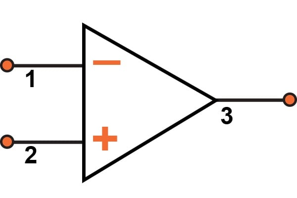
Fig 1.1 Op-amp symbol
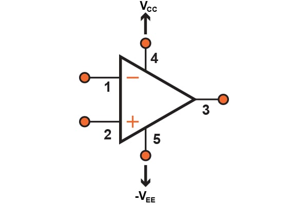
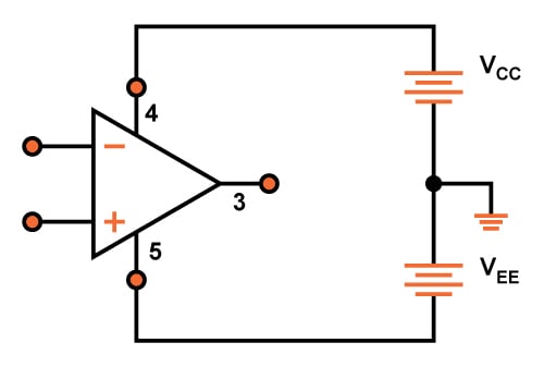
Fig 1.2 Op-amp connections to the dc power supplies
Besides the five terminals discussed thus far, an op-amp may have other terminals for specific purposes. Such purposes might be for frequency compensation and negative feedback or offset nulling, which reduces small DC offsets that can be amplified.
Introducing Characteristics of the Ideal Operational Amp
Looking at the actual functions of the circuit inside the op-amp, we see that it is designed to determine the difference between voltage signals that are applied directly to the two input terminals (the difference of v2 - v1). Once this quantity is found, it is then multiplied by a number A, and in turn, the voltage results in the term A(v2-v1). From here on out, when the voltage is referred to at the terminal, it is meant to be the voltage between that individual terminal and the ground; hence v1 is the voltage applied between terminal 1 and the ground.An ideal op-amp shouldn't be drawing any current for the inputs; meaning, the current into terminal 1 and signal into terminal 2 are both zero. This is to say that the input impedance of an ideal op-amp is supposed to be infinite.
Focusing on the output terminal now, it should act as though it is a terminal of an ideal voltage source. Simply put, the voltage across terminal 3 and ground will always equate to A(v2 - v1), and independent of the current that may or may not be drawn from the third terminal into a load impedance.
With all of this stated, a model can be illustrated for the op-amp shown in Fig 1.3. Looking at the model, one can see that the output terminal has the same sign as v2 but opposite sign of v1. With this in mind, the input terminal is called the inverting input terminal, being denoted by a "-" sign while the input terminal 2 is called the noninverting input terminal and is denoted by a "+" sign.
As stated before, the op-amp is designed to sense a difference between voltage signals and will ignore any given signal that is common to both inputs. What this means, is that if v1 = v2 = 1 V, then the output will accordingly (ideal) be zero. This phenomenon is also known as what's called common-mode rejection. This can also be stated as zero common-mode gain, or analogously, infinite common-mode rejection. For now, we can say that the op-amp is a differential input, single-ended output amplifier, with the latter term pertaining to the fact that this op amp's output lies between the ground and terminal 3.
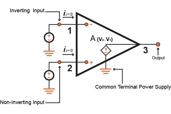
Figure 1.3 Circuit model of ideal op-amp
The term A, is what is known as the differential gain. It is known to be this because it is the desired gain of the op-amp when various signals are applied to the two inputs, 1 and 2. Another name that can we associated with the term is open-loop gain. This gain can be obtained when there is no feedback used in the IC op-amp. Normally, the open-loop gain tends to have an exceptionally high value; an ideal op-amp actually has an infinite open-loop gain.
One characteristic worth noting of op-amps are dc amplifiers or direct-coupled, which stands for dc or direct current since it amplifies signals with frequencies close to zero. Considering that op-amps are direct-coupled ICs, they are much more versatile which allows us to use them in many more important applications. However, direct-coupling can cause some serious problems that will be discussed later on.
Moving over to bandwidth, an ideal op-amp has gain A that will remain constant to a frequency of zero and all the way to an infinite frequency. In other words, an ideal amp can amplify signals of any frequency with an equal gain which allows them to have infinite bandwidth. Thus far, all characteristics and properties of ideal op-amps have been discussed, except one: the gain, A, of an ideal op-amp should have a value that is large and infinite, ideally speaking. However, this brings a good question: if there is a gain of an infinite value, how can the op-amp be used in any application? This can be answered rather simply because the op-amp will not be used solely in an open-loop configuration in almost every application one could think of. In the following article, I will discuss how other components will come into play by applying a feedback to complete or close the loop around the op-amp.
Summary
As of now, we have discussed how an operational amplifier is so popular due to its versatility, as well as the characteristics and functions of the ideal op-amp. To summarize, the characteristics of an ideal op-amp are as follows:- Infinite bandwidth due to the ideal gain inside of the op-amp
- Infinite open-loop gain A
- Infinite or zero common-mode gain
- Input impedance of an infinite value
- Output impedance of zero

Q . I Operational Amplifier Basics
As well as resistors and capacitors, Operational Amplifiers, or Op-amps as they are more commonly called, are one of the basic building blocks of Analogue Electronic Circuits.Operational amplifiers are linear devices that have all the properties required for nearly ideal DC amplification and are therefore used extensively in signal conditioning, filtering or to perform mathematical operations such as add, subtract, integration and differentiation.
An Operational Amplifier, or op-amp for short, is fundamentally a voltage amplifying device designed to be used with external feedback components such as resistors and capacitors between its output and input terminals. These feedback components determine the resulting function or “operation” of the amplifier and by virtue of the different feedback configurations whether resistive, capacitive or both, the amplifier can perform a variety of different operations, giving rise to its name of “Operational Amplifier”.
An Operational Amplifier is basically a three-terminal device which consists of two high impedance inputs, one called the Inverting Input, marked with a negative or “minus” sign, ( – ) and the other one called the Non-inverting Input, marked with a positive or “plus” sign ( + ).
Related Products: OP Amp | SP Amplifier
The third terminal represents the operational amplifiers output port which can both sink and source either a voltage or a current. In a linear operational amplifier, the output signal is the amplification factor, known as the amplifiers gain ( A ) multiplied by the value of the input signal and depending on the nature of these input and output signals, there can be four different classifications of operational amplifier gain.
- Voltage – Voltage “in” and Voltage “out”
- Current – Current “in” and Current “out”
- Transconductance – Voltage “in” and Current “out”
- Transresistance – Current “in” and Voltage “out”
The output voltage signal from an Operational Amplifier is the difference between the signals being applied to its two individual inputs. In other words, an op-amps output signal is the difference between the two input signals as the input stage of an Operational Amplifier is in fact a differential amplifier as shown below.
Differential Amplifier
The circuit below shows a generalized form of a differential amplifier with two inputs marked V1 and V2. The two identical transistors TR1 and TR2 are both biased at the same operating point with their emitters connected together and returned to the common rail, -Vee by way of resistor Re.
Differential Amplifier
So as the forward bias of transistor, TR1 is increased, the forward bias of transistor TR2 is reduced and vice versa. Then if the two transistors are perfectly matched, the current flowing through the common emitter resistor, Re will remain constant.
Like the input signal, the output signal is also balanced and since the collector voltages either swing in opposite directions (anti-phase) or in the same direction (in-phase) the output voltage signal, taken from between the two collectors is, assuming a perfectly balanced circuit the zero difference between the two collector voltages.
This is known as the Common Mode of Operation with the common mode gain of the amplifier being the output gain when the input is zero.
Operational Amplifiers also have one output (although there are ones with an additional differential output) of low impedance that is referenced to a common ground terminal and it should ignore any common mode signals that is, if an identical signal is applied to both the inverting and non-inverting inputs there should no change to the output.
However, in real amplifiers there is always some variation and the ratio of the change to the output voltage with regards to the change in the common mode input voltage is called the Common Mode Rejection Ratio or CMRR.
Operational Amplifiers on their own have a very high open loop DC gain and by applying some form of Negative Feedback we can produce an operational amplifier circuit that has a very precise gain characteristic that is dependant only on the feedback used. Note that the term “open loop” means that there are no feedback components used around the amplifier so the feedback path or loop is open.
An operational amplifier only responds to the difference between the voltages on its two input terminals, known commonly as the “Differential Input Voltage” and not to their common potential. Then if the same voltage potential is applied to both terminals the resultant output will be zero. An Operational Amplifiers gain is commonly known as the Open Loop Differential Gain, and is given the symbol (Ao).
Related Products: Audio Amplifier
Equivalent Circuit of an Ideal Operational Amplifier

Op-amp Parameter and Idealised Characteristic
Open Loop Gain, (Avo)
- Infinite – The main function of an operational amplifier is to amplify the input signal and the more open loop gain it has the better. Open-loop gain is the gain of the op-amp without positive or negative feedback and for such an amplifier the gain will be infinite but typical real values range from about 20,000 to 200,000.
Input impedance, (Zin)
- Infinite – Input impedance is the ratio of input voltage to input current and is assumed to be infinite to prevent any current flowing from the source supply into the amplifiers input circuitry ( Iin = 0 ). Real op-amps have input leakage currents from a few pico-amps to a few milli-amps.
Output impedance, (Zout)
- Zero – The output impedance of the ideal operational amplifier is assumed to be zero acting as a perfect internal voltage source with no internal resistance so that it can supply as much current as necessary to the load. This internal resistance is effectively in series with the load thereby reducing the output voltage available to the load. Real op-amps have output impedances in the 100-20kΩ range.
Bandwidth, (BW)
- Infinite – An ideal operational amplifier has an infinite frequency response and can amplify any frequency signal from DC to the highest AC frequencies so it is therefore assumed to have an infinite bandwidth. With real op-amps, the bandwidth is limited by the Gain-Bandwidth product (GB), which is equal to the frequency where the amplifiers gain becomes unity.
Offset Voltage, (Vio)
- Zero – The amplifiers output will be zero when the voltage difference between the inverting and the non-inverting inputs is zero, the same or when both inputs are grounded. Real op-amps have some amount of output offset voltage.
However, real Operational Amplifiers such as the commonly available uA741, for example do not have infinite gain or bandwidth but have a typical “Open Loop Gain” which is defined as the amplifiers output amplification without any external feedback signals connected to it and for a typical operational amplifier is about 100dB at DC (zero Hz). This output gain decreases linearly with frequency down to “Unity Gain” or 1, at about 1MHz and this is shown in the following open loop gain response curve.
Open-loop Frequency Response Curve

GBP = Gain x Bandwidth = A x BW
GBP = A x BW = 10 x 100,000Hz = 1,000,000.
GBP = A x BW = 1,000 x 1,000Hz = 1,000,000. The same!.

and in Decibels or (dB) is given as:

An Operational Amplifiers Bandwidth
The operational amplifiers bandwidth is the frequency range over which the voltage gain of the amplifier is above 70.7% or -3dB (where 0dB is the maximum) of its maximum output value as shown below.
Operational Amplifier Example No1.
Using the formula 20 log (A), we can calculate the bandwidth of the amplifier as:
37 = 20 log A therefore, A = anti-log (37 ÷ 20) = 70.8
GBP ÷ A = Bandwidth, therefore, 1,000,000 ÷ 70.8 = 14,124Hz, or 14kHz
Then the bandwidth of the amplifier at a gain of 40dB is given as 14kHz as previously predicted from the graph.Operational Amplifier Example No2.
If the gain of the operational amplifier was reduced by half to say 20dB in the above frequency response curve, the -3dB point would now be at 17dB. This would then give the operational amplifier an overall gain of 7.08, therefore A = 7.08.If we use the same formula as above, this new gain would give us a bandwidth of approximately 141.2kHz, ten times more than the frequency given at the 40dB point. It can therefore be seen that by reducing the overall “open loop gain” of an operational amplifier its bandwidth is increased and visa versa.
In other words, an operational amplifiers bandwidth is inversely proportional to its gain, ( A 1/∝ BW ). Also, this -3dB corner frequency point is generally known as the “half power point”, as the output power of the amplifier is at half its maximum value as shown:

Operational Amplifiers Summary
We know now that an Operational amplifiers is a very high gain DC differential amplifier that uses one or more external feedback networks to control its response and characteristics. We can connect external resistors or capacitors to the op-amp in a number of different ways to form basic “building Block” circuits such as, Inverting, Non-Inverting, Voltage Follower, Summing, Differential, Integrator and Differentiator type amplifiers.
Op-amp Symbol
There are a very large number of operational amplifier IC’s available to suit every possible application from standard bipolar, precision, high-speed, low-noise, high-voltage, etc, in either standard configuration or with internal Junction FET transistors.
Operational amplifiers are available in IC packages of either single, dual or quad op-amps within one single device. The most commonly available and used of all operational amplifiers in basic electronic kits and projects is the industry standard μA-741.


Q . II Inverting Operational Amplifier
We saw in the last tutorial that the Open Loop Gain, ( Avo ) of an operational amplifier can be very high, as much as 1,000,000 (120dB) or more.
However, this very high gain is of no real use to us as it makes the amplifier both unstable and hard to control as the smallest of input signals, just a few micro-volts, (μV) would be enough to cause the output voltage to saturate and swing towards one or the other of the voltage supply rails losing complete control of the output.
As the open loop DC gain of an operational amplifier is extremely high we can therefore afford to lose some of this high gain by connecting a suitable resistor across the amplifier from the output terminal back to the inverting input terminal to both reduce and control the overall gain of the amplifier. This then produces and effect known commonly as Negative Feedback, and thus produces a very stable Operational Amplifier based system.
Negative Feedback is the process of “feeding back” a fraction of the output signal back to the input, but to make the feedback negative, we must feed it back to the negative or “inverting input” terminal of the op-amp using an external Feedback Resistor called Rƒ. This feedback connection between the output and the inverting input terminal forces the differential input voltage towards zero.
This effect produces a closed loop circuit to the amplifier resulting in the gain of the amplifier now being called its Closed-loop Gain. Then a closed-loop inverting amplifier uses negative feedback to accurately control the overall gain of the amplifier, but at a cost in the reduction of the amplifiers gain.
This negative feedback results in the inverting input terminal having a different signal on it than the actual input voltage as it will be the sum of the input voltage plus the negative feedback voltage giving it the label or term of a Summing Point. We must therefore separate the real input signal from the inverting input by using an Input Resistor, Rin.
As we are not using the positive non-inverting input this is connected to a common ground or zero voltage terminal as shown below, but the effect of this closed loop feedback circuit results in the voltage potential at the inverting input being equal to that at the non-inverting input producing a Virtual Earth summing point because it will be at the same potential as the grounded reference input. In other words, the op-amp becomes a “differential amplifier”.
Inverting Operational Amplifier Configuration

This is because the junction of the input and feedback signal ( X ) is at the same potential as the positive ( + ) input which is at zero volts or ground then, the junction is a “Virtual Earth”. Because of this virtual earth node the input resistance of the amplifier is equal to the value of the input resistor, Rin and the closed loop gain of the inverting amplifier can be set by the ratio of the two external resistors.
We said above that there are two very important rules to remember about Inverting Amplifiers or any operational amplifier for that matter and these are.
- No Current Flows into the Input Terminals
- The Differential Input Voltage is Zero as V1 = V2 = 0 (Virtual Earth)
Current ( i ) flows through the resistor network as shown.


and this can be transposed to give Vout as:


Linear Output
The equation for the output voltage Vout also shows that the circuit is linear in nature for a fixed amplifier gain as Vout = Vin x Gain. This property can be very useful for converting a smaller sensor signal to a much larger voltage.
Another useful application of an inverting amplifier is that of a “transresistance amplifier” circuit. A Transresistance Amplifier also known as a “transimpedance amplifier”, is basically a current-to-voltage converter (Current “in” and Voltage “out”). They can be used in low-power applications to convert a very small current generated by a photo-diode or photo-detecting device etc, into a usable output voltage which is proportional to the input current as shown.
Transresistance Amplifier Circuit

Inverting Op-amp Example No1
Find the closed loop gain of the following inverting amplifier circuit.

Using the previously found formula for the gain of the circuit
we can now substitute the values of the resistors in the circuit as follows,
Rin = 10kΩ and Rƒ = 100kΩ.
and the gain of the circuit is calculated as: -Rƒ/Rin = 100k/10k = -10.Therefore, the closed loop gain of the inverting amplifier circuit above is given -10 or 20dB (20log(10)).
Inverting Op-amp Example No2
The gain of the original circuit is to be increased to 40 (32dB), find the new values of the resistors required.Assume that the input resistor is to remain at the same value of 10KΩ, then by re-arranging the closed loop voltage gain formula we can find the new value required for the feedback resistor Rƒ.
Gain = Rƒ/Rin
therefore, Rƒ = Gain x Rin
Rƒ = 40 x 10,000
Rƒ = 400,000 or 400KΩ
The new values of resistors required for the circuit to have a gain of 40 would be,
Rin = 10KΩ and Rƒ = 400KΩ.
The formula could also be rearranged to give a new value of Rin, keeping the same value of Rƒ.One final point to note about the Inverting Amplifier configuration for an operational amplifier, if the two resistors are of equal value, Rin = Rƒ then the gain of the amplifier will be -1 producing a complementary form of the input voltage at its output as Vout = -Vin. This type of inverting amplifier configuration is generally called a Unity Gain Inverter of simply an Inverting Buffer.
In the next tutorial about Operational Amplifiers, we will analyse the complement of the Inverting Amplifier operational amplifier circuit called the Non-inverting Amplifier that produces an output signal which is “in-phase” with the input.

Q . III Non-inverting Operational Amplifier
The second basic configuration of an operational amplifier circuit is that of a Non-inverting Operational Amplifier design.
In this configuration, the input voltage signal, ( Vin ) is applied directly to the non-inverting ( + ) input terminal which means that the output gain of the amplifier becomes “Positive” in value in contrast to the “Inverting Amplifier” circuit we saw in the last tutorial whose output gain is negative in value. The result of this is that the output signal is “in-phase” with the input signal.
Feedback control of the non-inverting operational amplifier is achieved by applying a small part of the output voltage signal back to the inverting ( – ) input terminal via a Rƒ – R2 voltage divider network, again producing negative feedback. This closed-loop configuration produces a non-inverting amplifier circuit with very good stability, a very high input impedance, Rin approaching infinity, as no current flows into the positive input terminal, (ideal conditions) and a low output impedance, Rout as shown below.
Non-inverting Operational Amplifier Configuration

In other words the junction is a “virtual earth” summing point. Because of this virtual earth node the resistors, Rƒ and R2 form a simple potential divider network across the non-inverting amplifier with the voltage gain of the circuit being determined by the ratios of R2 and Rƒ as shown below.
Equivalent Potential Divider Network


If the value of the feedback resistor Rƒ is zero, the gain of the amplifier will be exactly equal to one (unity). If resistor R2 is zero the gain will approach infinity, but in practice it will be limited to the operational amplifiers open-loop differential gain, ( Ao ).
We can easily convert an inverting operational amplifier configuration into a non-inverting amplifier configuration by simply changing the input connections as shown.

Voltage Follower (Unity Gain Buffer)
If we made the feedback resistor, Rƒ equal to zero, (Rƒ = 0), and resistor R2 equal to infinity, (R2 = ∞), then the circuit would have a fixed gain of “1” as all the output voltage would be present on the inverting input terminal (negative feedback). This would then produce a special type of the non-inverting amplifier circuit called a Voltage Follower or also called a “unity gain buffer”.As the input signal is connected directly to the non-inverting input of the amplifier the output signal is not inverted resulting in the output voltage being equal to the input voltage, Vout = Vin. This then makes the voltage follower circuit ideal as a Unity Gain Buffer circuit because of its isolation properties.
The advantage of the unity gain voltage follower is that it can be used when impedance matching or circuit isolation is more important than amplification as it maintains the signal voltage. The input impedance of the voltage follower circuit is very high, typically above 1MΩ as it is equal to that of the operational amplifiers input resistance times its gain ( Rin x Ao ). Also its output impedance is very low since an ideal op-amp condition is assumed.
Non-inverting Voltage Follower


Since the input current is zero giving zero input power, the voltage follower can provide a large power gain. However in most real unity gain buffer circuits a low value (typically 1kΩ) resistor is required to reduce any offset input leakage currents, and also if the operational amplifier is of a current feedback type.
The voltage follower or unity gain buffer is a special and very useful type of Non-inverting amplifier circuit that is commonly used in electronics to isolated circuits from each other especially in High-order state variable or Sallen-Key type active filters to separate one filter stage from the other. Typical digital buffer IC’s available are the 74LS125 Quad 3-state buffer or the more common 74LS244 Octal buffer.
One final thought, the closed loop voltage gain of a voltage follower circuit is “1” or Unity. The open loop voltage gain of an operational amplifier with no feedback is Infinite. Then by carefully selecting the feedback components we can control the amount of gain produced by a non-inverting operational amplifier anywhere from one to infinity.
Thus far we have analysed an inverting and non-inverting amplifier circuit that has just one input signal, Vin. In the next tutorial about Operational Amplifiers, we will examine the effect of the output voltage, Vout by connecting more inputs to the amplifier. This then produces another common type of operational amplifier circuit called a Summing Amplifier which can be used to “add” together the voltages present on its inputs.
Q . IIII The Summing Amplifier

The Summing Amplifier is another type of operational amplifier circuit configuration that is used to combine the voltages present on two or more inputs into a single output voltage
We saw previously in the inverting operational amplifier that the inverting amplifier has a single input voltage, (Vin) applied to the inverting input terminal. If we add more input resistors to the input, each equal in value to the original input resistor, (Rin) we end up with another operational amplifier circuit called a Summing Amplifier, “summing inverter” or even a “voltage adder” circuit as shown below.
Summing Amplifier Circuit


However, if all the input impedances, ( Rin ) are equal in value, we can simplify the above equation to give an output voltage of:
Summing Amplifier Equation

This is because the input signals are effectively isolated from each other by the “virtual earth” node at the inverting input of the op-amp. A direct voltage addition can also be obtained when all the resistances are of equal value and Rƒ is equal to Rin.
Note that when the summing point is connected to the inverting input of the op-amp the circuit will produce the negative sum of any number of input voltages. Likewise, when the summing point is connected to the non-inverting input of the op-amp, it will produce the positive sum of the input voltages.
A Scaling Summing Amplifier can be made if the individual input resistors are “NOT” equal. Then the equation would have to be modified to:


Sometimes we need a summing circuit to just add together two or more voltage signals without any amplification. By putting all of the resistances of the circuit above to the same value R, the op-amp will have a voltage gain of unity and an output voltage equal to the direct sum of all the input voltages as shown:

Summing Amplifier Example No1
Find the output voltage of the following Summing Amplifier circuit.Summing Amplifier


Summing Amplifier Applications
So what can we use summing amplifiers for?. If the input resistances of a summing amplifier are connected to potentiometers the individual input signals can be mixed together by varying amounts.For example, measuring temperature, you could add a negative offset voltage to make the output voltage or display read “0” at the freezing point or produce an audio mixer for adding or mixing together individual waveforms (sounds) from different source channels (vocals, instruments, etc) before sending them combined to an audio amplifier.
Summing Amplifier Audio Mixer

Digital to Analogue Converter

Also, the accuracy of this full-scale analogue output depends on voltage levels of the input bits being consistently 0V for “0” and consistently 5V for “1” as well as the accuracy of the resistance values used for the input resistors, Rin.
Fortunately to overcome these errors, at least on our part, commercially available Digital-to Analogue and Analogue-to Digital devices are readily available with highly accurate resistor ladder networks already built-in.
In the next tutorial about operational amplifiers, we will examine the effect of the output voltage, Vout when a signal voltage is connected to the inverting input and the non-inverting input at the same time to produce another common type of operational amplifier circuit called a Differential Amplifier which can be used to “subtract” the voltages present on its inputs.
Q . IIIII The Differential Amplifier

Thus far we have used only one of the operational amplifiers inputs to connect to the amplifier, using either the “inverting” or the “non-inverting” input terminal to amplify a single input signal with the other input being connected to ground.
But as a standard operational amplifier has two inputs, inverting and no-inverting, we can also connect signals to both of these inputs at the same time producing another common type of operational amplifier circuit called a Differential Amplifier.
Basically, as we saw in the first tutorial about operational amplifiers, all op-amps are “Differential Amplifiers” due to their input configuration. But by connecting one voltage signal onto one input terminal and another voltage signal onto the other input terminal the resultant output voltage will be proportional to the “Difference” between the two input voltage signals of V1 and V2.
Related Products: OP Amp | SP Amplifier
Then differential amplifiers amplify the difference between two voltages making this type of operational amplifier circuit a Subtractor unlike a summing amplifier which adds or sums together the input voltages. This type of operational amplifier circuit is commonly known as a Differential Amplifier configuration and is shown below:
Differential Amplifier


Differential Amplifier Equation

The Differential Amplifier circuit is a very useful op-amp circuit and by adding more resistors in parallel with the input resistors R1 and R3, the resultant circuit can be made to either “Add” or “Subtract” the voltages applied to their respective inputs. One of the most common ways of doing this is to connect a “Resistive Bridge” commonly called a Wheatstone Bridge to the input of the amplifier as shown below.
Wheatstone Bridge Differential Amplifier

Light Activated Differential Amplifier

The voltage value at V1 sets the op-amps trip point with a feed back potentiometer, VR2 used to set the switching hysteresis. That is the difference between the light level for “ON” and the light level for “OFF”.
The second leg of the differential amplifier consists of a standard light dependant resistor, also known as a LDR, photoresistive sensor that changes its resistive value (hence its name) with the amount of light on its cell as their resistive value is a function of illumination.
The LDR can be any standard type of cadmium-sulphide (cdS) photoconductive cell such as the common NORP12 that has a resistive range of between about 500Ω in sunlight to about 20kΩ’s or more in the dark.
The NORP12 photoconductive cell has a spectral response similar to that of the human eye making it ideal for use in lighting control type applications. The photocell resistance is proportional to the light level and falls with increasing light intensity so therefore the voltage level at V2 will also change above or below the switching point which can be determined by the position of VR1.
Then by adjusting the light level trip or set position using potentiometer VR1 and the switching hysteresis using potentiometer, VR2 an precision light-sensitive switch can be made. Depending upon the application, the output from the op-amp can switch the load directly, or use a transistor switch to control a relay or the lamps themselves.
It is also possible to detect temperature using this type of simple circuit configuration by replacing the light dependant resistor with a thermistor. By interchanging the positions of VR1 and the LDR, the circuit can be used to detect either light or dark, or heat or cold using a thermistor.
One major limitation of this type of amplifier design is that its input impedances are lower compared to that of other operational amplifier configurations, for example, a non-inverting (single-ended input) amplifier.
Each input voltage source has to drive current through an input resistance, which has less overall impedance than that of the op-amps input alone. This may be good for a low impedance source such as the bridge circuit above, but not so good for a high impedance source.
One way to overcome this problem is to add a Unity Gain Buffer Amplifier such as the voltage follower seen in the previous tutorial to each input resistor. This then gives us a differential amplifier circuit with very high input impedance and low output impedance as it consists of two non-inverting buffers and one differential amplifier. This then forms the basis for most “Instrumentation Amplifiers”.
Instrumentation Amplifier
Instrumentation Amplifiers (in-amps) are very high gain differential amplifiers which have a high input impedance and a single ended output. Instrumentation amplifiers are mainly used to amplify very small differential signals from strain gauges, thermocouples or current sensing devices in motor control systems.Unlike standard operational amplifiers in which their closed-loop gain is determined by an external resistive feedback connected between their output terminal and one input terminal, either positive or negative, “instrumentation amplifiers” have an internal feedback resistor that is effectively isolated from its input terminals as the input signal is applied across two differential inputs, V1 and V2.
The instrumentation amplifier also has a very good common mode rejection ratio, CMRR (zero output when V1 = V2) well in excess of 100dB at DC. A typical example of a three op-amp instrumentation amplifier with a high input impedance ( Zin ) is given below:
High Input Impedance Instrumentation Amplifier

As the op-amps take no current at their input terminals (virtual earth), the same current must flow through the three resistor network of R2, R1 and R2 connected across the op-amp outputs. This means then that the voltage on the upper end of R1 will be equal to V1 and the voltage at the lower end of R1 to be equal to V2.
This produces a voltage drop across resistor R1 which is equal to the voltage difference between inputs V1 and V2, the differential input voltage, because the voltage at the summing junction of each amplifier, Va and Vb is equal to the voltage applied to its positive inputs.
However, if a common-mode voltage is applied to the amplifiers inputs, the voltages on each side of R1 will be equal, and no current will flow through this resistor. Since no current flows through R1 (nor, therefore, through both R2 resistors, amplifiers A1 and A2 will operate as unity-gain followers (buffers). Since the input voltage at the outputs of amplifiers A1 and A2 appears differentially across the three resistor network, the differential gain of the circuit can be varied by just changing the value of R1.
The voltage output from the differential op-amp A3 acting as a subtractor, is simply the difference between its two inputs ( V2 – V1 ) and which is amplified by the gain of A3 which may be one, unity, (assuming that R3 = R4). Then we have a general expression for overall voltage gain of the instrumentation amplifier circuit as:
Instrumentation Amplifier Equation

Q . IIIIIII The Integrator Amplifier

In the previous tutorials we have seen circuits which show how an operational amplifier can be used as part of a positive or negative feedback amplifier or as an adder or subtractor type circuit using just pure resistances in both the input and the feedback loop.
But what if we were to change the purely resistive ( Rƒ ) feedback element of an inverting amplifier to that of a frequency dependant impedance, ( Z ) type complex element, such as a Capacitor, C. What would be the effect on the op-amps output voltage over its frequency range.
By replacing this feedback resistance with a capacitor we now have an RC Network connected across the operational amplifiers feedback path producing another type of operational amplifier circuit commonly called an Op-amp Integrator circuit as shown below.
Related Products: Analog Divider and Multiplier | Comparator
Op-amp Integrator Circuit

In other words the magnitude of the output signal is determined by the length of time a voltage is present at its input as the current through the feedback loop charges or discharges the capacitor as the required negative feedback occurs through the capacitor.
Related Products: OP Amp, SP Amplifier
When a step voltage, Vin is firstly applied to the input of an integrating amplifier, the uncharged capacitor C has very little resistance and acts a bit like a short circuit allowing maximum current to flow via the input resistor, Rin as potential difference exists between the two plates. No current flows into the amplifiers input and point X is a virtual earth resulting in zero output. As the impedance of the capacitor at this point is very low, the gain ratio of Xc/Rin is also very small giving an overall voltage gain of less than one, ( voltage follower circuit ).
As the feedback capacitor, C begins to charge up due to the influence of the input voltage, its impedance Xc slowly increase in proportion to its rate of charge. The capacitor charges up at a rate determined by the RC time constant, ( τ ) of the series RC network. Negative feedback forces the op-amp to produce an output voltage that maintains a virtual earth at the op-amp’s inverting input.
Since the capacitor is connected between the op-amp’s inverting input (which is at earth potential) and the op-amp’s output (which is negative), the potential voltage, Vc developed across the capacitor slowly increases causing the charging current to decrease as the impedance of the capacitor increases. This results in the ratio of Xc/Rin increasing producing a linearly increasing ramp output voltage that continues to increase until the capacitor is fully charged.
At this point the capacitor acts as an open circuit, blocking any more flow of DC current. The ratio of feedback capacitor to input resistor ( Xc/Rin ) is now infinite resulting in infinite gain. The result of this high gain (similar to the op-amps open-loop gain), is that the output of the amplifier goes into saturation as shown below. (Saturation occurs when the output voltage of the amplifier swings heavily to one voltage supply rail or the other with little or no control in between).


Op-amp Integrator Ramp Generator


The AC or Continuous Op-amp Integrator
If we changed the above square wave input signal to that of a sine wave of varying frequency the Op-amp Integrator performs less like an integrator and begins to behave more like an active “Low Pass Filter”, passing low frequency signals while attenuating the high frequencies.At 0Hz or DC, the capacitor acts like an open circuit blocking any feedback voltage resulting in very little negative feedback from the output back to the input of the amplifier. Then with just the feedback capacitor, C, the amplifier effectively is connected as a normal open-loop amplifier which has very high open-loop gain resulting in the output voltage saturating.
This circuit connects a high value resistance in parallel with a continuously charging and discharging capacitor. The addition of this feedback resistor, R2 across the capacitor, C gives the circuit the characteristics of an inverting amplifier with finite closed-loop gain of R2/R1. The result is at very low frequencies the circuit acts as an standard integrator, while at higher frequencies the capacitor shorts out the feedback resistor, R2 due to the effects of capacitive reactance reducing the amplifiers gain.
The AC Op-amp Integrator with DC Gain Control

Further more, when the input is triangular, the output waveform is also sinusoidal. This then forms the basis of a Active Low Pass Filter as seen before in the filters section tutorials with a corner frequency given as.

Q . IIIIIIII The Differentiator Amplifier

Here, the position of the capacitor and resistor have been reversed and now the reactance, Xc is connected to the input terminal of the inverting amplifier while the resistor, Rƒ forms the negative feedback element across the operational amplifier as normal.
This operational amplifier circuit performs the mathematical operation of Differentiation, that is it “produces a voltage output which is directly proportional to the input voltage’s rate-of-change with respect to time“. In other words the faster or larger the change to the input voltage signal, the greater the input current, the greater will be the output voltage change in response, becoming more of a “spike” in shape.
As with the integrator circuit, we have a resistor and capacitor forming an RC Network across the operational amplifier and the reactance ( Xc ) of the capacitor plays a major role in the performance of a Op-amp Differentiator.
 The input signal to the differentiator is applied to the capacitor. The capacitor blocks any DC content so there is no current flow to the amplifier summing point, X resulting in zero output voltage. The capacitor only allows AC type input voltage changes to pass through and whose frequency is dependant on the rate of change of the input signal.
At low frequencies the reactance of the capacitor is “High” resulting in a low gain ( Rƒ/Xc ) and low output voltage from the op-amp. At higher frequencies the reactance of the capacitor is much lower resulting in a higher gain and higher output voltage from the differentiator amplifier.
However, at high frequencies an op-amp differentiator circuit becomes unstable and will start to oscillate. This is due mainly to the first-order effect, which determines the frequency response of the op-amp circuit causing a second-order response which, at high frequencies gives an output voltage far higher than what would be expected. To avoid this the high frequency gain of the circuit needs to be reduced by adding an additional small value capacitor across the feedback resistor Rƒ.
Ok, some math’s to explain what’s going on!. Since the node voltage of the operational amplifier at its inverting input terminal is zero, the current, i flowing through the capacitor will be given as:
 The charge on the capacitor equals Capacitance x Voltage across the capacitor
 The rate of change of this charge is:
 but dQ/dt is the capacitor current,i
 from which we have an ideal voltage output for the op-amp differentiator is given as:
 Therefore, the output voltage Vout is a constant -Rƒ.C times the derivative of the input voltage Vin with respect to time. The minus sign indicates a 180o phase shift because the input signal is connected to the inverting input terminal of the operational amplifier.
One final point to mention, the Op-amp Differentiator circuit in its basic form has two main disadvantages compared to the previous operational amplifier integrator circuit. One is that it suffers from instability at high frequencies as mentioned above, and the other is that the capacitive input makes it very susceptible to random noise signals and any noise or harmonics present in the source circuit will be amplified more than the input signal itself. This is because the output is proportional to the slope of the input voltage so some means of limiting the bandwidth in order to achieve closed-loop stability is required.

 Adding the input resistor Rin limits the differentiators increase in gain at a ratio of Rƒ/Rin. The circuit now acts like a differentiator amplifier at low frequencies and an amplifier with resistive feedback at high frequencies giving much better noise rejection.
Additional attenuation of higher frequencies is accomplished by connecting a capacitor Cƒ in parallel with the differentiator feedback resistor, Rƒ. This then forms the basis of a Active High Pass Filter as we have seen before in the filters section.
Q . IIIIIIIIII Operational Amplifier Building Blocks

We have seen that we can connect resistors to a basic operational amplifier to produce various inverting and non-inverting outputs and configurations along with their respective gains.
So to make things a little bit easier for all, here is a list of some of the “Basic Operational Amplifier Building Blocks” we can use to create different electronic circuits and filters.


If the magnitudes of the two op-amp gains, A1 and A2 are equal to each other, then the output signal will be doubled as it is effectively the combination of the two individual amplifier gains.


If resistances are equal (R = R3 and RA = R4) then the output voltage is as given and the voltage gain is +1. If the input resistance are unequal the circuit becomes a differential amplifier producing a negative output when V1 is higher than V2 and a positive output when V1 is lower than V2.

When the input voltage drops below the preset reference voltage and Vin < Vref, the output switches back. By using positive feedback the basic comparator circuit can easily be converted into a Schmitt Trigger to reduce oscillations around the switching point.
 Here are just some of the more common and basic operational amplifier building block configurations discussed in this section that we can use in electronic circuits. All the above circuits can be constructed using a variety of different op-amps including the famous 741 op-amp. I hope that this short tutorial about basic op-amp building blocks will help you to understand the different basic op-amp circuit configurations.
 timeline1941: A vacuum tube op-amp. An op-amp, defined as a general-purpose, DC-coupled, high gain, inverting feedback amplifier, is first found in U.S. Patent 2,401,779 "Summing Amplifier" filed by Karl D. Swartzel Jr. of Bell Labs in 1941. This design used three vacuum tubes to achieve a gain of 90 dB and operated on voltage rails of ±350 V. It had a single inverting input rather than differential inverting and non-inverting inputs, as are common in today's op-amps. Throughout World War II, Swartzel's design proved its value by being liberally used in the M9 artillery director designed at Bell Labs. This artillery director worked with the SCR584 radar system to achieve extraordinary hit rates (near 90%) that would not have been possible otherwise.[16]
1947: An op-amp with an explicit non-inverting input. In 1947, the operational amplifier was first formally defined and named in a paper[17] by John R. Ragazzini of Columbia University. In this same paper a footnote mentioned an op-amp design by a student that would turn out to be quite significant. This op-amp, designed by Loebe Julie, was superior in a variety of ways. It had two major innovations. Its input stage used a long-tailed triode pair with loads matched to reduce drift in the output and, far more importantly, it was the first op-amp design to have two inputs (one inverting, the other non-inverting). The differential input made a whole range of new functionality possible, but it would not be used for a long time due to the rise of the chopper-stabilized amplifier.[16]
1949: A chopper-stabilized op-amp. In 1949, Edwin A. Goldberg designed a chopper-stabilized op-amp.[18] This set-up uses a normal op-amp with an additional AC amplifier that goes alongside the op-amp. The chopper gets an AC signal from DC by switching between the DC voltage and ground at a fast rate (60 Hz or 400 Hz). This signal is then amplified, rectified, filtered and fed into the op-amp's non-inverting input. This vastly improved the gain of the op-amp while significantly reducing the output drift and DC offset. Unfortunately, any design that used a chopper couldn't use their non-inverting input for any other purpose. Nevertheless, the much improved characteristics of the chopper-stabilized op-amp made it the dominant way to use op-amps. Techniques that used the non-inverting input regularly would not be very popular until the 1960s when op-amp ICs started to show up in the field.
1953: A commercially available op-amp. In 1953, vacuum tube op-amps became commercially available with the release of the model K2-W from George A. Philbrick Researches, Incorporated. The designation on the devices shown, GAP/R, is an acronym for the complete company name. Two nine-pin 12AX7 vacuum tubes were mounted in an octal package and had a model K2-P chopper add-on available that would effectively "use up" the non-inverting input. This op-amp was based on a descendant of Loebe Julie's 1947 design and, along with its successors, would start the widespread use of op-amps in industry.
1961: A discrete IC op-amp. With the birth of the transistor in 1947, and the silicon transistor in 1954, the concept of ICs became a reality. The introduction of the planar process in 1959 made transistors and ICs stable enough to be commercially useful. By 1961, solid-state, discrete op-amps were being produced. These op-amps were effectively small circuit boards with packages such as edge connectors. They usually had hand-selected resistors in order to improve things such as voltage offset and drift. The P45 (1961) had a gain of 94 dB and ran on ±15 V rails. It was intended to deal with signals in the range of ±10 V.
1961: A varactor bridge op-amp. There have been many different directions taken in op-amp design. Varactor bridge op-amps started to be produced in the early 1960s.[19][20] They were designed to have extremely small input current and are still amongst the best op-amps available in terms of common-mode rejection with the ability to correctly deal with hundreds of volts at their inputs.
1962: An op-amp in a potted module. By 1962, several companies were producing modular potted packages that could be plugged into printed circuit boards.[citation needed] These packages were crucially important as they made the operational amplifier into a single black box which could be easily treated as a component in a larger circuit.
1963: A monolithic IC op-amp. In 1963, the first monolithic IC op-amp, the μA702 designed by Bob Widlar at Fairchild Semiconductor, was released. Monolithic ICs consist of a single chip as opposed to a chip and discrete parts (a discrete IC) or multiple chips bonded and connected on a circuit board (a hybrid IC). Almost all modern op-amps are monolithic ICs; however, this first IC did not meet with much success. Issues such as an uneven supply voltage, low gain and a small dynamic range held off the dominance of monolithic op-amps until 1965 when the μA709[21] (also designed by Bob Widlar) was released.
1968: Release of the μA741. The popularity of monolithic op-amps was further improved upon the release of the LM101 in 1967, which solved a variety of issues, and the subsequent release of the μA741 in 1968. The μA741 was extremely similar to the LM101 except that Fairchild's facilities allowed them to include a 30 pF compensation capacitor inside the chip instead of requiring external compensation. This simple difference has made the 741 the canonical op-amp and many modern amps base their pinout on the 741s. The μA741 is still in production, and has become ubiquitous in electronics—many manufacturers produce a version of this classic chip, recognizable by part numbers containing 741. The same part is manufactured by several companies.
1970: First high-speed, low-input current FET design. In the 1970s high speed, low-input current designs started to be made by using FETs. These would be largely replaced by op-amps made with MOSFETs in the 1980s.
1972: Single sided supply op-amps being produced. A single sided supply op-amp is one where the input and output voltages can be as low as the negative power supply voltage instead of needing to be at least two volts above it. The result is that it can operate in many applications with the negative supply pin on the op-amp being connected to the signal ground, thus eliminating the need for a separate negative power supply.
The LM324 (released in 1972) was one such op-amp that came in a quad package (four separate op-amps in one package) and became an industry standard. In addition to packaging multiple op-amps in a single package, the 1970s also saw the birth of op-amps in hybrid packages. These op-amps were generally improved versions of existing monolithic op-amps. As the properties of monolithic op-amps improved, the more complex hybrid ICs were quickly relegated to systems that are required to have extremely long service lives or other specialty systems.
Recent trends. Recently supply voltages in analog circuits have decreased (as they have in digital logic) and low-voltage op-amps have been introduced reflecting this. Supplies of 5 V and increasingly 3.3 V (sometimes as low as 1.8 V) are common. To maximize the signal range modern op-amps commonly have rail-to-rail output (the output signal can range from the lowest supply voltage to the highest) and sometimes rail-to-rail inputs.


This operational amplifier circuit performs the mathematical operation of Differentiation, that is it “produces a voltage output which is directly proportional to the input voltage’s rate-of-change with respect to time“. In other words the faster or larger the change to the input voltage signal, the greater the input current, the greater will be the output voltage change in response, becoming more of a “spike” in shape.
As with the integrator circuit, we have a resistor and capacitor forming an RC Network across the operational amplifier and the reactance ( Xc ) of the capacitor plays a major role in the performance of a Op-amp Differentiator.
Op-amp Differentiator Circuit
At low frequencies the reactance of the capacitor is “High” resulting in a low gain ( Rƒ/Xc ) and low output voltage from the op-amp. At higher frequencies the reactance of the capacitor is much lower resulting in a higher gain and higher output voltage from the differentiator amplifier.
However, at high frequencies an op-amp differentiator circuit becomes unstable and will start to oscillate. This is due mainly to the first-order effect, which determines the frequency response of the op-amp circuit causing a second-order response which, at high frequencies gives an output voltage far higher than what would be expected. To avoid this the high frequency gain of the circuit needs to be reduced by adding an additional small value capacitor across the feedback resistor Rƒ.
Ok, some math’s to explain what’s going on!. Since the node voltage of the operational amplifier at its inverting input terminal is zero, the current, i flowing through the capacitor will be given as:
One final point to mention, the Op-amp Differentiator circuit in its basic form has two main disadvantages compared to the previous operational amplifier integrator circuit. One is that it suffers from instability at high frequencies as mentioned above, and the other is that the capacitive input makes it very susceptible to random noise signals and any noise or harmonics present in the source circuit will be amplified more than the input signal itself. This is because the output is proportional to the slope of the input voltage so some means of limiting the bandwidth in order to achieve closed-loop stability is required.
Op-amp Differentiator Waveforms
If we apply a constantly changing signal such as a Square-wave, Triangular or Sine-wave type signal to the input of a differentiator amplifier circuit the resultant output signal will be changed and whose final shape is dependant upon the RC time constant of the Resistor/Capacitor combination.Improved Op-amp Differentiator Amplifier
The basic single resistor and single capacitor op-amp differentiator circuit is not widely used to reform the mathematical function of Differentiation because of the two inherent faults mentioned above, “Instability” and “Noise”. So in order to reduce the overall closed-loop gain of the circuit at high frequencies, an extra resistor, Rin is added to the input as shown below.Improved Op-amp Differentiator Amplifier
Additional attenuation of higher frequencies is accomplished by connecting a capacitor Cƒ in parallel with the differentiator feedback resistor, Rƒ. This then forms the basis of a Active High Pass Filter as we have seen before in the filters section.
Q . IIIIIIIIII Operational Amplifier Building Blocks
We have seen that we can connect resistors to a basic operational amplifier to produce various inverting and non-inverting outputs and configurations along with their respective gains.
So to make things a little bit easier for all, here is a list of some of the “Basic Operational Amplifier Building Blocks” we can use to create different electronic circuits and filters.
The Voltage Follower
The Voltage Follower, also called a buffer dose not amplify or invert the input signal but instead provides isolation between two circuits. The input impedance is very high while the output impedance is low avoiding any loading effects within the circuit. As the output is connected back directly to one of the inputs, the overall gain of the buffer is +1 and Vout = Vin.The Voltage Follower Op-amp Circuit
The Op-amp Inverter
The Inverter, also called an inverting buffer is the opposite to that of the previous voltage follower. The inverter does not amplify if both resistances are equal but does invert the input signal. The input impedance is equal to R and the gain is -1 giving Vout = -Vin.The Op-amp Inverter Circuit
The Non-inverting Amplifier
The Non-inverting Amplifier does not invert the input signal or produce an inverting signal but instead amplifies it by the ratio of: (RA + RB)/RB or commonly 1+(RA/RB). The input signal is connected to the non-inverting (+) input.The Non-inverting Op-amp Circuit
The Inverting Amplifier
The Inverting Amplifier both inverts and amplifies the input signal by the ratio of -RA/RB. The gain of the amplifier is controlled by negative feedback using the feedback resistor RA and the input signal is fed to the inverting (–) input.The Inverting Op-amp Circuit
The Bridge Amplifier
The inverting and non-inverting amplifier circuits from above can be connected together to form a bridge amplifier configuration. The input signal is common to both op-amps with the output voltage signal taken across the load resistor, RL which floats between the two outputs.If the magnitudes of the two op-amp gains, A1 and A2 are equal to each other, then the output signal will be doubled as it is effectively the combination of the two individual amplifier gains.
The Bridge Op-amp Circuit
The Voltage Adder
The Adder, also called a summing amplifier, produces an inverted output voltage which is proportional to the sum of the input voltages V1 and V2. More inputs can be summed. If the input resistors are equal in value (R1 = R2 = R) then the summed output voltage is as given and the gain is +1. If the input resistors are unequal then the output voltage is a weighted sum and becomes:
Vout = -(V1(RA/R1) + V2(RA/R2) + etc.)
The Voltage Adder Op-amp Circuit
The Voltage Subtractor
The Subtractor also called a differential amplifier, uses both the inverting and non-inverting inputs to produce an output signal which is the difference between the two input voltages V1 and V2 allowing one signal to be subtracted from another. More inputs can be added to be subtracted if required.If resistances are equal (R = R3 and RA = R4) then the output voltage is as given and the voltage gain is +1. If the input resistance are unequal the circuit becomes a differential amplifier producing a negative output when V1 is higher than V2 and a positive output when V1 is lower than V2.
The Voltage Subtractor Op-amp Circuit
The Op-amp Comparator
The Comparator has many uses but the most common is to compare the input voltage to a reference voltage and switch the output if the input voltage is above the reference voltage. If the input goes more positive than the reference voltage set by the voltage divider, Vin > Vref, the output changes state.When the input voltage drops below the preset reference voltage and Vin < Vref, the output switches back. By using positive feedback the basic comparator circuit can easily be converted into a Schmitt Trigger to reduce oscillations around the switching point.
The Comparator Op-amp Circuit
Q . IIIIIIIII Op-amp Multivibrator
The Operational Amplifier or Op-amp for short, is a very versatile device that can be used in a variety of different electronic circuits and applications, from voltage amplifiers, to filters, to signal conditioners
But one very simple and extremely useful op-amp circuit based around any general purpose operational amplifier is the Astable Op-amp Multivibrator.
We saw in our tutorials about Sequential Logic that multivibrator circuits can be constructed using transistors, logic gates or from dedicated chips such as the NE555 timer. We also saw that the astable multivibrator switches continuously between its two unstable states without the need for any external triggering.
But the problem with using these components to produce an astable multivibrator circuit is that for transistor based astables, many additional components are required, digital astables can generally only be used in digital circuits, and the use of a 555 timer may not always give us a symmetrical output without additional biasing components. The Op-amp Multivibrator circuit however, can provide us with a good rectangular wave signal with the use of just four components, three resistors and a timing capacitor.
The Op-amp Multivibrator is an astable oscillator circuit that generates a rectangular output waveform using an RC timing network connected to the inverting input of the operational amplifier and a voltage divider network connected to the other non-inverting input.
Unlike the monostable or bistable, the astable multivibrator has two states, neither of which are stable as it is constantly switching between these two states with the time spent in each state controlled by the charging or discharging of the capacitor through a resistor.
In the op-amp multivibrator circuit the op-amp works as an analogue comparator. An op-amp comparator compares the voltages on its two inputs and gives a positive or negative output depending on whether the input is greater or less than some reference value, Vref.
However, because the open-loop op-amp comparator is very sensitive to the voltage changes on its inputs, the output can switch uncontrollably between its positive, +V(sat) and negative, -V(sat) supply rails whenever the input voltage being measured is near to the reference voltage, Vref.
To eliminate any erratic or uncontrolled switching operations, the op-amp used in the multivibrator circuit is configured as a closed-loop Schmitt Trigger circuit. Consider the circuit below.
 The op-amp comparator circuit above is configured as a Schmitt trigger that uses positive feedback provided by resistors R1 and R2 to generate hysteresis. As this resistive network is connected between the amplifiers output and non-inverting (+) input, when Vout is saturated at the positive supply rail, a positive voltage is applied to the op-amps non-inverting input. Likewise, when Vout is saturated to the negative supply rail, a negative voltage is applied to the op-amps non-inverting input.
As the two resistors are configured across the op-amps output as a voltage divider network, the reference voltage, Vref will therefore be dependant upon the fraction of output voltage fed back to the non-inverting input. This feedback fraction, β is given as:
 Where +V(sat) is the positive op-amp DC saturation voltage and -V(sat) is the negative op-amp DC saturation voltage.
Then we can see that the positive or upper reference voltage, +Vref (i.e. the maximum positive value for the voltage at the inverting input) is given as: +Vref = +V(sat)β while the negative or lower reference voltage (i.e. the maximum negative value for the voltage at the inverting input) is given as: -Vref = -V(sat)β.
So if Vin exceeds +Vref, the op-amp switches state and the output voltage drops to its negative DC saturation voltage. Likewise when the input voltage falls below -Vref, the op-amp switches state once again and the output voltage will switch from the negative saturation voltage back to the positive DC saturation voltage. The amount of built-in hysteresis given by the Schmitt comparator as it switches between the two saturation voltages is defined by the difference between the two trigger reference voltages as: VHYSTERESIS = +Vref - (-Vref).
In fact the Schmitt comparator will always produce a rectangular output waveform independent of the input signal waveform. In other words, the voltage input does not have to be a sinusoid, it could be any wave shape or complex waveform. Consider the circuit below.
 As the input waveform will be periodical and have an amplitude sufficiently greater than its reference voltage, Vref, the output rectangular waveform will always have the same period, T and therefore frequency, ƒ as the input waveform.
By replacing either resistor R1 or R2 with a potentiometer we could adjust the feedback fraction, β and therefore the reference voltage value at the non-inverting input to cause the op-amp to change state anywhere from zero to 90o of each half cycle so long as the reference voltage, Vref remained below the maximum amplitude of the input signal.
 So how does it work. Firstly lets assume that the capacitor is fully discharged and the output of the op-amp is saturated at the positive supply rail. The capacitor, C starts to charge up from the output voltage, Vout through resistor, R at a rate determined by their RC time constant.
We know from our tutorials about RC circuits that the capacitor wants to charge up fully to the value of Vout (which is +V(sat)) within five time constants. However, as soon as the capacitors charging voltage at the op-amps inverting (-) terminal is equal to or greater than the voltage at the non-inverting terminal (the op-amps output voltage fraction divided between resistors R1 and R2), the output will change state and be driven to the opposing negative supply rail.
But the capacitor, which has been happily charging towards the positive supply rail (+V(sat)), now sees a negative voltage, -V(sat) across its plates. This sudden reversal of the output voltage causes the capacitor to discharge toward the new value of Vout at a rate dictated again by their RC time constant.
 Once the op-amps inverting terminal reaches the new negative reference voltage, -Vref at the non-inverting terminal, the op-amp once again changes state and the output is driven to the opposing supply rail voltage, +V(sat). The capacitor now see’s a positive voltage across its plates and the charging cycle begins again. Thus, the capacitor is constantly charging and discharging creating an astable op-amp multivibrator output.
The period of the output waveform is determined by the RC time constant of the two timing components and the feedback ratio established by the R1, R2 voltage divider network which sets the reference voltage level. If the positive and negative values of the amplifiers saturation voltage have the same magnitude, then t1 = t2 and the expression to give the period of oscillation becomes:
 Then we can see from the above equation that the frequency of oscillation for an Op-amp Multivibrator circuit not only depends upon the RC time constant but also upon the feedback fraction. However, if we used resistor values that gave a feedback fraction of 0.462, (β = 0.462), then the frequency of oscillation of the circuit would be equal to just 1/2RC as shown because the linear log term becomes equal to one.

 Then the frequency of oscillation is calculated as 1kHz. When β = 0.462, this frequency can be calculated directly as: ƒ = 1/2RC. Also when the two feedback resistors are the same, that is R1 = R2, the feedback fraction is equal to 3 and the frequency of oscillation becomes: ƒ = 1/2.2RC.
We can take this op-amp multivibrator circuit one step further by replacing one of the feedback resistors with a potentiometer to produce a variable frequency op-amp multivibrator as shown.
 By adjusting the central potentiometer between β1 and β2 the output frequency will change by the following amounts.
Potentiometer wiper at β1
 Potentiometer wiper at β2
 Then in this simple example we can produce an operational amplifier multivibrator circuit that can produce a variable output rectangular waveform from 100Hz to 1.2kHz, or any frequency range we require just by changing the RC component values.
We have seen above that an Op-amp Multivibrator circuit can be constructed using a standard operational amplifier, such as the 741, and a few additional components. These voltage controlled non-sinusoidal relaxation oscillators are generally limited to a few hundred kilo-hertz (kHz) because the op-amp does not have the required bandwidth, but nevertheless they still make excellent oscillators.
We saw in our tutorials about Sequential Logic that multivibrator circuits can be constructed using transistors, logic gates or from dedicated chips such as the NE555 timer. We also saw that the astable multivibrator switches continuously between its two unstable states without the need for any external triggering.
But the problem with using these components to produce an astable multivibrator circuit is that for transistor based astables, many additional components are required, digital astables can generally only be used in digital circuits, and the use of a 555 timer may not always give us a symmetrical output without additional biasing components. The Op-amp Multivibrator circuit however, can provide us with a good rectangular wave signal with the use of just four components, three resistors and a timing capacitor.
The Op-amp Multivibrator is an astable oscillator circuit that generates a rectangular output waveform using an RC timing network connected to the inverting input of the operational amplifier and a voltage divider network connected to the other non-inverting input.
Unlike the monostable or bistable, the astable multivibrator has two states, neither of which are stable as it is constantly switching between these two states with the time spent in each state controlled by the charging or discharging of the capacitor through a resistor.
In the op-amp multivibrator circuit the op-amp works as an analogue comparator. An op-amp comparator compares the voltages on its two inputs and gives a positive or negative output depending on whether the input is greater or less than some reference value, Vref.
However, because the open-loop op-amp comparator is very sensitive to the voltage changes on its inputs, the output can switch uncontrollably between its positive, +V(sat) and negative, -V(sat) supply rails whenever the input voltage being measured is near to the reference voltage, Vref.
To eliminate any erratic or uncontrolled switching operations, the op-amp used in the multivibrator circuit is configured as a closed-loop Schmitt Trigger circuit. Consider the circuit below.
Op-amp Schmitt Comparator
As the two resistors are configured across the op-amps output as a voltage divider network, the reference voltage, Vref will therefore be dependant upon the fraction of output voltage fed back to the non-inverting input. This feedback fraction, β is given as:
Then we can see that the positive or upper reference voltage, +Vref (i.e. the maximum positive value for the voltage at the inverting input) is given as: +Vref = +V(sat)β while the negative or lower reference voltage (i.e. the maximum negative value for the voltage at the inverting input) is given as: -Vref = -V(sat)β.
So if Vin exceeds +Vref, the op-amp switches state and the output voltage drops to its negative DC saturation voltage. Likewise when the input voltage falls below -Vref, the op-amp switches state once again and the output voltage will switch from the negative saturation voltage back to the positive DC saturation voltage. The amount of built-in hysteresis given by the Schmitt comparator as it switches between the two saturation voltages is defined by the difference between the two trigger reference voltages as: VHYSTERESIS = +Vref - (-Vref).
Sinusoidal to Rectangular Conversion
One of the many uses of a Schmitt trigger comparator, other than as an op-amp multivibrator, is that we can use it to convert any periodic sinusoidal waveform into a rectangular waveform providing the value of the sinusoid is greater than the voltage reference point.In fact the Schmitt comparator will always produce a rectangular output waveform independent of the input signal waveform. In other words, the voltage input does not have to be a sinusoid, it could be any wave shape or complex waveform. Consider the circuit below.
Sinusoidal to Rectangular Converter
By replacing either resistor R1 or R2 with a potentiometer we could adjust the feedback fraction, β and therefore the reference voltage value at the non-inverting input to cause the op-amp to change state anywhere from zero to 90o of each half cycle so long as the reference voltage, Vref remained below the maximum amplitude of the input signal.
Op-amp Multivibrator
We can take this idea of converting a periodic waveform into a rectangular output one step further by replacing the sinusoidal input with an RC timing circuit connected across the op-amps output. This time, instead of a sinusoidal waveform being used to trigger the op-amp, we can use the capacitors charging voltage, Vc to change the output state of the op-amp as shown.Op-amp Multivibrator Circuit
We know from our tutorials about RC circuits that the capacitor wants to charge up fully to the value of Vout (which is +V(sat)) within five time constants. However, as soon as the capacitors charging voltage at the op-amps inverting (-) terminal is equal to or greater than the voltage at the non-inverting terminal (the op-amps output voltage fraction divided between resistors R1 and R2), the output will change state and be driven to the opposing negative supply rail.
But the capacitor, which has been happily charging towards the positive supply rail (+V(sat)), now sees a negative voltage, -V(sat) across its plates. This sudden reversal of the output voltage causes the capacitor to discharge toward the new value of Vout at a rate dictated again by their RC time constant.
Op-amp Multivibrator Voltages
The period of the output waveform is determined by the RC time constant of the two timing components and the feedback ratio established by the R1, R2 voltage divider network which sets the reference voltage level. If the positive and negative values of the amplifiers saturation voltage have the same magnitude, then t1 = t2 and the expression to give the period of oscillation becomes:
Example No1
An op-amp multivibrator circuit is constructed using the following components. R1 = 35kΩ, R2 = 30kΩ, R = 50kΩ and C = 0.01uF. Calculate the circuits frequency of oscillation.We can take this op-amp multivibrator circuit one step further by replacing one of the feedback resistors with a potentiometer to produce a variable frequency op-amp multivibrator as shown.
Variable Op-amp Multivibrator
Potentiometer wiper at β1
We have seen above that an Op-amp Multivibrator circuit can be constructed using a standard operational amplifier, such as the 741, and a few additional components. These voltage controlled non-sinusoidal relaxation oscillators are generally limited to a few hundred kilo-hertz (kHz) because the op-amp does not have the required bandwidth, but nevertheless they still make excellent oscillators.
Q . IIIIIIIIII But one very simple and extremely useful op-amp circuit based around any general purpose operational amplifier is the Astable Op-amp Multivibrator.
We saw in our tutorials about Sequential Logic that multivibrator circuits can be constructed using transistors, logic gates or from dedicated chips such as the NE555 timer. We also saw that the astable multivibrator switches continuously between its two unstable states without the need for any external triggering.
But the problem with using these components to produce an astable multivibrator circuit is that for transistor based astables, many additional components are required, digital astables can generally only be used in digital circuits, and the use of a 555 timer may not always give us a symmetrical output without additional biasing components. The Op-amp Multivibrator circuit however, can provide us with a good rectangular wave signal with the use of just four components, three resistors and a timing capacitor.
The Op-amp Multivibrator is an astable oscillator circuit that generates a rectangular output waveform using an RC timing network connected to the inverting input of the operational amplifier and a voltage divider network connected to the other non-inverting input.
Unlike the monostable or bistable, the astable multivibrator has two states, neither of which are stable as it is constantly switching between these two states with the time spent in each state controlled by the charging or discharging of the capacitor through a resistor.
In the op-amp multivibrator circuit the op-amp works as an analogue comparator. An op-amp comparator compares the voltages on its two inputs and gives a positive or negative output depending on whether the input is greater or less than some reference value, Vref.
However, because the open-loop op-amp comparator is very sensitive to the voltage changes on its inputs, the output can switch uncontrollably between its positive, +V(sat) and negative, -V(sat) supply rails whenever the input voltage being measured is near to the reference voltage, Vref.
To eliminate any erratic or uncontrolled switching operations, the op-amp used in the multivibrator circuit is configured as a closed-loop Schmitt Trigger circuit. Consider the circuit below.
The op-amp comparator circuit above is configured as a Schmitt trigger that uses positive feedback provided by resistors R1 and R2 to generate hysteresis. As this resistive network is connected between the amplifiers output and non-inverting (+) input, when Vout is saturated at the positive supply rail, a positive voltage is applied to the op-amps non-inverting input. Likewise, when Vout is saturated to the negative supply rail, a negative voltage is applied to the op-amps non-inverting input.
As the two resistors are configured across the op-amps output as a voltage divider network, the reference voltage, Vref will therefore be dependant upon the fraction of output voltage fed back to the non-inverting input. This feedback fraction, β is given as:
Where +V(sat) is the positive op-amp DC saturation voltage and -V(sat) is the negative op-amp DC saturation voltage.
Then we can see that the positive or upper reference voltage, +Vref (i.e. the maximum positive value for the voltage at the inverting input) is given as: +Vref = +V(sat)β while the negative or lower reference voltage (i.e. the maximum negative value for the voltage at the inverting input) is given as: -Vref = -V(sat)β.
So if Vin exceeds +Vref, the op-amp switches state and the output voltage drops to its negative DC saturation voltage. Likewise when the input voltage falls below -Vref, the op-amp switches state once again and the output voltage will switch from the negative saturation voltage back to the positive DC saturation voltage. The amount of built-in hysteresis given by the Schmitt comparator as it switches between the two saturation voltages is defined by the difference between the two trigger reference voltages as: VHYSTERESIS = +Vref - (-Vref).
In fact the Schmitt comparator will always produce a rectangular output waveform independent of the input signal waveform. In other words, the voltage input does not have to be a sinusoid, it could be any wave shape or complex waveform. Consider the circuit below.
As the input waveform will be periodical and have an amplitude sufficiently greater than its reference voltage, Vref, the output rectangular waveform will always have the same period, T and therefore frequency, ƒ as the input waveform.
By replacing either resistor R1 or R2 with a potentiometer we could adjust the feedback fraction, β and therefore the reference voltage value at the non-inverting input to cause the op-amp to change state anywhere from zero to 90o of each half cycle so long as the reference voltage, Vref remained below the maximum amplitude of the input signal.
So how does it work. Firstly lets assume that the capacitor is fully discharged and the output of the op-amp is saturated at the positive supply rail. The capacitor, C starts to charge up from the output voltage, Vout through resistor, R at a rate determined by their RC time constant.
We know from our tutorials about RC circuits that the capacitor wants to charge up fully to the value of Vout (which is +V(sat)) within five time constants. However, as soon as the capacitors charging voltage at the op-amps inverting (-) terminal is equal to or greater than the voltage at the non-inverting terminal (the op-amps output voltage fraction divided between resistors R1 and R2), the output will change state and be driven to the opposing negative supply rail.
But the capacitor, which has been happily charging towards the positive supply rail (+V(sat)), now sees a negative voltage, -V(sat) across its plates. This sudden reversal of the output voltage causes the capacitor to discharge toward the new value of Vout at a rate dictated again by their RC time constant.
Once the op-amps inverting terminal reaches the new negative reference voltage, -Vref at the non-inverting terminal, the op-amp once again changes state and the output is driven to the opposing supply rail voltage, +V(sat). The capacitor now see’s a positive voltage across its plates and the charging cycle begins again. Thus, the capacitor is constantly charging and discharging creating an astable op-amp multivibrator output.
The period of the output waveform is determined by the RC time constant of the two timing components and the feedback ratio established by the R1, R2 voltage divider network which sets the reference voltage level. If the positive and negative values of the amplifiers saturation voltage have the same magnitude, then t1 = t2 and the expression to give the period of oscillation becomes:
Then we can see from the above equation that the frequency of oscillation for an Op-amp Multivibrator circuit not only depends upon the RC time constant but also upon the feedback fraction. However, if we used resistor values that gave a feedback fraction of 0.462, (β = 0.462), then the frequency of oscillation of the circuit would be equal to just 1/2RC as shown because the linear log term becomes equal to one.
Then the frequency of oscillation is calculated as 1kHz. When β = 0.462, this frequency can be calculated directly as: ƒ = 1/2RC. Also when the two feedback resistors are the same, that is R1 = R2, the feedback fraction is equal to 3 and the frequency of oscillation becomes: ƒ = 1/2.2RC.
We can take this op-amp multivibrator circuit one step further by replacing one of the feedback resistors with a potentiometer to produce a variable frequency op-amp multivibrator as shown.
By adjusting the central potentiometer between β1 and β2 the output frequency will change by the following amounts.
Potentiometer wiper at β1
Potentiometer wiper at β2
Then in this simple example we can produce an operational amplifier multivibrator circuit that can produce a variable output rectangular waveform from 100Hz to 1.2kHz, or any frequency range we require just by changing the RC component values.
We have seen above that an Op-amp Multivibrator circuit can be constructed using a standard operational amplifier, such as the 741, and a few additional components. These voltage controlled non-sinusoidal relaxation oscillators are generally limited to a few hundred kilo-hertz (kHz) because the op-amp does not have the required bandwidth, but nevertheless they still make excellent oscillators.


 Oscillators convert a DC input (the supply voltage) into an AC output (the waveform), which can have a wide range of different wave shapes and frequencies that can be either complicated in nature or simple sine waves depending upon the application.
Oscillators are also used in many pieces of test equipment producing either sinusoidal sine waves, square, sawtooth or triangular shaped waveforms or just a train of pulses of a variable or constant width. LC Oscillators are commonly used in radio-frequency circuits because of their good phase noise characteristics and their ease of implementation.
An Oscillator is basically an Amplifier with “Positive Feedback”, or regenerative feedback (in-phase) and one of the many problems in electronic circuit design is stopping amplifiers from oscillating while trying to get oscillators to oscillate.
Related Products: Oscillators and Crystals | Crystals | MEMS Oscillators | SMD Crystal Oscillator | TH Crystal Oscillator
Oscillators work because they overcome the losses of their feedback resonator circuit either in the form of a capacitor, inductor or both in the same circuit by applying DC energy at the required frequency into this resonator circuit. In other words, an oscillator is a an amplifier which uses positive feedback that generates an output frequency without the use of an input signal. It is self sustaining.
Then an oscillator has a small signal feedback amplifier with an open-loop gain equal too or slightly greater than one for oscillations to start but to continue oscillations the average loop gain must return to unity. In addition to these reactive components, an amplifying device such as an Operational Amplifier or Bipolar Transistor is required.
Unlike an amplifier there is no external AC input required to cause the Oscillator to work as the DC supply energy is converted by the oscillator into AC energy at the required frequency.


 Oscillators are circuits that generate a continuous voltage output waveform at a required frequency with the values of the inductors, capacitors or resistors forming a frequency selective LC resonant tank circuit and feedback network. This feedback network is an attenuation network which has a gain of less than one ( β <1 ) and starts oscillations when Aβ >1 which returns to unity ( Aβ =1 ) once oscillations commence.
The LC oscillators frequency is controlled using a tuned or resonant inductive/capacitive (LC) circuit with the resulting output frequency being known as the Oscillation Frequency. By making the oscillators feedback a reactive network the phase angle of the feedback will vary as a function of frequency and this is called Phase-shift.
There are basically types of Oscillators
At high frequencies the reactance of a capacitor is very low acting as a short circuit while the reactance of the inductor is high acting as an open circuit. At low frequencies the reverse is true, the reactance of the capacitor acts as an open circuit and the reactance of the inductor acts as a short circuit.
Between these two extremes the combination of the inductor and capacitor produces a “Tuned” or “Resonant” circuit that has a Resonant Frequency, ( ƒr ) in which the capacitive and inductive reactance’s are equal and cancel out each other, leaving only the resistance of the circuit to oppose the flow of current. This means that there is no phase shift as the current is in phase with the voltage. Consider the circuit below.
 The circuit consists of an inductive coil, L and a capacitor, C. The capacitor stores energy in the form of an electrostatic field and which produces a potential (static voltage) across its plates, while the inductive coil stores its energy in the form of an electromagnetic field. The capacitor is charged up to the DC supply voltage, V by putting the switch in position A. When the capacitor is fully charged the switch changes to position B.
The charged capacitor is now connected in parallel across the inductive coil so the capacitor begins to discharge itself through the coil. The voltage across C starts falling as the current through the coil begins to rise.
This rising current sets up an electromagnetic field around the coil which resists this flow of current. When the capacitor, C is completely discharged the energy that was originally stored in the capacitor, C as an electrostatic field is now stored in the inductive coil, L as an electromagnetic field around the coils windings.
As there is now no external voltage in the circuit to maintain the current within the coil, it starts to fall as the electromagnetic field begins to collapse. A back emf is induced in the coil (e = -Ldi/dt) keeping the current flowing in the original direction.
This current charges up capacitor, C with the opposite polarity to its original charge. C continues to charge up until the current reduces to zero and the electromagnetic field of the coil has collapsed completely.
The energy originally introduced into the circuit through the switch, has been returned to the capacitor which again has an electrostatic voltage potential across it, although it is now of the opposite polarity. The capacitor now starts to discharge again back through the coil and the whole process is repeated. The polarity of the voltage changes as the energy is passed back and forth between the capacitor and inductor producing an AC type sinusoidal voltage and current waveform.
This process then forms the basis of an LC oscillators tank circuit and theoretically this cycling back and forth will continue indefinitely. However, things are not perfect and every time energy is transferred from the capacitor, C to inductor, L and back from L to C some energy losses occur which decay the oscillations to zero over time.
This oscillatory action of passing energy back and forth between the capacitor, C to the inductor, L would continue indefinitely if it was not for energy losses within the circuit. Electrical energy is lost in the DC or real resistance of the inductors coil, in the dielectric of the capacitor, and in radiation from the circuit so the oscillation steadily decreases until they die away completely and the process stops.
Then in a practical LC circuit the amplitude of the oscillatory voltage decreases at each half cycle of oscillation and will eventually die away to zero. The oscillations are then said to be “damped” with the amount of damping being determined by the quality or Q-factor of the circuit.
 The frequency of the oscillatory voltage depends upon the value of the inductance and capacitance in the LC tank circuit. We now know that for resonance to occur in the tank circuit, there must be a frequency point were the value of XC, the capacitive reactance is the same as the value of XL, the inductive reactance ( XL = XC ) and which will therefore cancel out each other out leaving only the DC resistance in the circuit to oppose the flow of current.
If we now place the curve for inductive reactance of the inductor on top of the curve for capacitive reactance of the capacitor so that both curves are on the same frequency axes, the point of intersection will give us the resonance frequency point, ( ƒr or ωr ) as shown below.
 where: ƒr is in Hertz, L is in Henries and C is in Farads.
 Then by simplifying the above equation we get the final equation for Resonant Frequency, ƒr in a tuned LC circuit as:
 This equation shows that if either L or C are decreased, the frequency increases. This output frequency is commonly given the abbreviation of ( ƒr ) to identify it as the “resonant frequency”.
To keep the oscillations going in an LC tank circuit, we have to replace all the energy lost in each oscillation and also maintain the amplitude of these oscillations at a constant level. The amount of energy replaced must therefore be equal to the energy lost during each cycle.
If the energy replaced is too large the amplitude would increase until clipping of the supply rails occurs. Alternatively, if the amount of energy replaced is too small the amplitude would eventually decrease to zero over time and the oscillations would stop.
The simplest way of replacing this lost energy is to take part of the output from the LC tank circuit, amplify it and then feed it back into the LC circuit again. This process can be achieved using a voltage amplifier using an op-amp, FET or bipolar transistor as its active device. However, if the loop gain of the feedback amplifier is too small, the desired oscillation decays to zero and if it is too large, the waveform becomes distorted.
To produce a constant oscillation, the level of the energy fed back to the LC network must be accurately controlled. Then there must be some form of automatic amplitude or gain control when the amplitude tries to vary from a reference voltage either up or down.
To maintain a stable oscillation the overall gain of the circuit must be equal to one or unity. Any less and the oscillations will not start or die away to zero, any more the oscillations will occur but the amplitude will become clipped by the supply rails causing distortion. Consider the circuit below.
 A Bipolar Transistor is used as the LC oscillators amplifier with the tuned LC tank circuit acts as the collector load. Another coil L2 is connected between the base and the emitter of the transistor whose electromagnetic field is “mutually” coupled with that of coil L.
“Mutual inductance” exists between the two circuits and the changing current flowing in one coil circuit induces, by electromagnetic induction, a potential voltage in the other (transformer effect) so as the oscillations occur in the tuned circuit, electromagnetic energy is transferred from coil L to coil L2 and a voltage of the same frequency as that in the tuned circuit is applied between the base and emitter of the transistor. In this way the necessary automatic feedback voltage is applied to the amplifying transistor.
The amount of feedback can be increased or decreased by altering the coupling between the two coils L and L2. When the circuit is oscillating its impedance is resistive and the collector and base voltages are 180o out of phase. In order to maintain oscillations (called frequency stability) the voltage applied to the tuned circuit must be “in-phase” with the oscillations occurring in the tuned circuit.
Therefore, we must introduce an additional 180o phase shift into the feedback path between the collector and the base. This is achieved by winding the coil of L2 in the correct direction relative to coil L giving us the correct amplitude and phase relationships for the Oscillators circuit or by connecting a phase shift network between the output and input of the amplifier.
The LC Oscillator is therefore a “Sinusoidal Oscillator” or a “Harmonic Oscillator” as it is more commonly called. LC oscillators can generate high frequency sine waves for use in radio frequency (RF) type applications with the transistor amplifier being of a Bipolar Transistor or FET.
Harmonic Oscillators come in many different forms because there are many different ways to construct an LC filter network and amplifier with the most common being the Hartley LC Oscillator, Colpitts LC Oscillator, Armstrong Oscillator and Clapp Oscillator to name a few.
 Then we can see from the above example that by decreasing the value of either the capacitance, C or the inductance, L will have the effect of increasing the frequency of oscillation of the LC tank circuit.
Q . IIIIIIIIIII The Hartley Oscillator

One of the main disadvantages of the basic LC Oscillator circuit we looked at in the previous tutorial is that they have no means of controlling the amplitude of the oscillations and also, it is difficult to tune the oscillator to the required frequency. If the cumulative electromagnetic coupling between L1 and L2 is too small there would be insufficient feedback and the oscillations would eventually die away to zero.
Likewise if the feedback was too strong the oscillations would continue to increase in amplitude until they were limited by the circuit conditions producing signal distortion. So it becomes very difficult to “tune” the oscillator.
However, it is possible to feed back exactly the right amount of voltage for constant amplitude oscillations. If we feed back more than is necessary the amplitude of the oscillations can be controlled by biasing the amplifier in such a way that if the oscillations increase in amplitude, the bias is increased and the gain of the amplifier is reduced.
If the amplitude of the oscillations decreases the bias decreases and the gain of the amplifier increases, thus increasing the feedback. In this way the amplitude of the oscillations are kept constant using a process known as Automatic Base Bias.
One big advantage of automatic base bias in a voltage controlled oscillator, is that the oscillator can be made more efficient by providing a Class-B bias or even a Class-C bias condition of the transistor. This has the advantage that the collector current only flows during part of the oscillation cycle so the quiescent collector current is very small. Then this “self-tuning” base oscillator circuit forms one of the most common types of LC parallel resonant feedback oscillator configurations called the Hartley Oscillator circuit.

Hartley Oscillator Tank Circuit
In the Hartley Oscillator the tuned LC circuit is connected between the collector and the base of a transistor amplifier. As far as the oscillatory voltage is concerned, the emitter is connected to a tapping point on the tuned circuit coil.
The feedback part of the tuned LC tank circuit is taken from the centre tap of the inductor coil or even two separate coils in series which are in parallel with a variable capacitor, C as shown.
The Hartley circuit is often referred to as a split-inductance oscillator because coil L is centre-tapped. In effect, inductance L acts like two separate coils in very close proximity with the current flowing through coil section XY induces a signal into coil section YZ below.
An Hartley Oscillator circuit can be made from any configuration that uses either a single tapped coil (similar to an autotransformer) or a pair of series connected coils in parallel with a single capacitor as shown below.
 When the circuit is oscillating, the voltage at point X (collector), relative to point Y (emitter), is 180o out-of-phase with the voltage at point Z (base) relative to point Y. At the frequency of oscillation, the impedance of the Collector load is resistive and an increase in Base voltage causes a decrease in the Collector voltage.
Then there is a 180o phase change in the voltage between the Base and Collector and this along with the original 180o phase shift in the feedback loop provides the correct phase relationship of positive feedback for oscillations to be maintained.
The amount of feedback depends upon the position of the “tapping point” of the inductor. If this is moved nearer to the collector the amount of feedback is increased, but the output taken between the Collector and earth is reduced and vice versa. Resistors, R1 and R2 provide the usual stabilizing DC bias for the transistor in the normal manner while the capacitors act as DC-blocking capacitors.
In this Hartley Oscillator circuit, the DC Collector current flows through part of the coil and for this reason the circuit is said to be “Series-fed” with the frequency of oscillation of the Hartley Oscillator being given as.
 Note: LT is the total cumulatively coupled inductance if two separate coils are used including their mutual inductance, M.
The frequency of oscillations can be adjusted by varying the “tuning” capacitor, C or by varying the position of the iron-dust core inside the coil (inductive tuning) giving an output over a wide range of frequencies making it very easy to tune. Also the Hartley Oscillator produces an output amplitude which is constant over the entire frequency range.
As well as the Series-fed Hartley Oscillator above, it is also possible to connect the tuned tank circuit across the amplifier as a shunt-fed oscillator as shown below.
 In the shunt-fed Hartley oscillator circuit, both the AC and DC components of the Collector current have separate paths around the circuit. Since the DC component is blocked by the capacitor, C2 no DC flows through the inductive coil, L and less power is wasted in the tuned circuit.
The Radio Frequency Coil (RFC), L2 is an RF choke which has a high reactance at the frequency of oscillations so that most of the RF current is applied to the LC tuning tank circuit via capacitor, C2 as the DC component passes through L2 to the power supply. A resistor could be used in place of the RFC coil, L2 but the efficiency would be less.
From above we can calculate the frequency of oscillations for a Hartley Oscillator as:
 The circuit consists of two inductive coils in series, so the total inductance is given as:


 The advantage of constructing a Hartley Oscillator using an operational amplifier as its active stage is that the gain of the op-amp can be very easily adjusted using the feedback resistors R1 and R2. As with the transistorised oscillator above, the gain of the circuit must be equal too or slightly greater than the ratio of L1/L2. If the two inductive coils are wound onto a common core and mutual inductance M exists then the ratio becomes (L1+M)/(L2+M).
This Hartley Oscillator configuration has a tuned tank circuit with its resonant coil tapped to feed a fraction of the output signal back to the emitter of the transistor. Since the output of the transistors emitter is always “in-phase” with the output at the collector, this feedback signal is positive. The oscillating frequency which is a sine-wave voltage is determined by the resonance frequency of the tank circuit.
Q . IIIIIIIIIIII Linear Integrated Circuit Questions and Answers – Ideal Operational Amplifier
This set of Linear Integrated Circuit Multiple Choice Questions & Answers (MCQs) focuses on “Ideal Operational Amplifier”.
1. Determine the output from the following circuit

a) 180o in phase with input signal
b) 180o out of phase with input signal
c) Same as that of input signal
d) Output signal cannot be determined
View Answer
a) Infinite voltage gain
b) Infinite bandwidth
c) Infinite output resistance
d) Infinite slew rate
View Answer
a) Signals can be amplified without attenuation
b) Output common-mode noise voltage is zero
c) Output voltage occurs simultaneously with input voltage changes
d) Output can drive infinite number of device
View Answer
a) To control the output voltage
b) To obtain finite output voltage
c) To receive zero noise output voltage
d) None of the mentioned
View Answer

a)
b)
c)
d) None of the mentioned
View Answer
a) VO= V1-V2
b) VO= A×(V1-V2)
c) VO= A×(V1+V2)
d) VO= V1×V2
View Answer
a) Amplifies the difference between the two input voltages
b) Amplifies individual voltages input voltages
c) Amplifies products of two input voltage
d) None of the mentioned
View Answer

a) Data provided is insufficient
b)
c)
d)
View Answer
a) Input Resistance –> 0
b) Output impedance –> 0
c) Bandwidth –> ∞
d) Open loop voltage gain –> ∞
View Answer
a)
b)
c)
d)
View Answer
a) 8v
b) 4v
c) -4v
d) -2v
View Answer
a) Positive saturation
b) Negative saturation
c) Both positive and negative saturation voltage
d) Supply voltage
View Answer
 Sourced by many manufacturers, and in multiple similar products, an example of a bipolar transistor operational amplifier is the 741 integrated circuit designed in 1968 by David Fullagar at Fairchild Semiconductor after Bob Widlar's LM301 integrated circuit design.[10] In this discussion, we use the parameters of the Hybrid-pi model to characterize the small-signal, grounded emitter characteristics of a transistor. In this model, the current gain of a transistor is denoted hfe, more commonly called the β.
It entails two cascaded transistor pairs, satisfying conflicting requirements. The first stage consists of the matched NPN emitter follower pair Q1, Q2 that provide high input impedance. The second is the matched PNP common-base pair Q3, Q4 that eliminates the undesirable Miller effect; it drives an active load Q7 plus matched pair Q5, Q6.
That active load is implemented as a modified Wilson current mirror; its role is to convert the (differential) input current signal to a single-ended signal without the attendant 50% losses (increasing the op-amp's open-loop gain by 3 dB).[nb 4] Thus, a small-signal differential current in Q3 versus Q4 appears summed (doubled) at the base of Q15, the input of the voltage gain stage.
The transistor Q22 prevents this stage from delivering excessive current to Q20 and thus limits the output sink current.
The resistor (39 kΩ) connecting the (diode-connected) Q11 and Q12, and the given supply voltage (VS+−VS−), determine the current in the current mirrors, (matched pairs) Q10/Q11 and Q12/Q13. The collector current of Q11, i11 * 39 kΩ = VS+ − VS− − 2 VBE. For the typical VS = ±20 V, the standing current in Q11/Q12 (as well as in Q13) would be ≈1 mA. A supply current for a typical 741 of about 2 mA agrees with the notion that these two bias currents dominate the quiescent supply current.
Transistors Q11 and Q10 form a Widlar current mirror, with quiescent current in Q10 i10 such that ln( i11 / i10 ) = i10 * 5 kΩ / 28 mV, where 5 kΩ represents the emitter resistor of Q10, and 28 mV is VT, the thermal voltage at room temperature. In this case i10 ≈ 20 μA.
The quiescent currents of Q1/Q3 (resp., Q2/Q4) i1 will thus be half of i10, of order ≈ 10 μA. Input bias current for the base of Q1 (resp. Q2) will amount to i1 / β; typically ≈50 nA, implying a current gain hfe ≈ 200 for Q1(Q2).
This feedback circuit tends to draw the common base node of Q3/Q4 to a voltage Vcom − 2 * VBE, where Vcom is the input common-mode voltage. At the same time, the magnitude of the quiescent current is relatively insensitive to the characteristics of the components Q1–Q4, such as hfe, that would otherwise cause temperature dependence or part-to-part variations.
Transistor Q7 drives Q5 and Q6 into conduction until their (equal) collector currents match that of Q1/Q3 and Q2/Q4. The quiescent current in Q7 is VBE / 50 kΩ, about 35μA, as is the quiescent current in Q15, with its matching operating point. Thus, the quiescent currents are pairwise matched in Q1/Q2, Q3/Q4, Q5/Q6, and Q7/Q15.
This portion of the op amp cleverly changes a differential signal at the op amp inputs to a single-ended signal at the base of Q15, and in a way that avoids wastefully discarding the signal in either leg. To see how, notice that a small negative change in voltage at the inverting input (Q2 base) drives it out of conduction, and this incremental decrease in current passes directly from Q4 collector to its emitter, resulting in a decrease in base drive for Q15. On the other hand, a small positive change in voltage at the non-inverting input (Q1 base) drives this transistor into conduction, reflected in an increase in current at the collector of Q3. This current drives Q7 further into conduction, which turns on current mirror Q5/Q6. Thus, the increase in Q3 emitter current is mirrored in an increase in Q6 collector current; the increased collector currents shunts more from the collector node and results in a decrease in base drive current for Q15. Besides avoiding wasting 3 dB of gain here, this technique decreases common-mode gain and feedthrough of power supply noise.
The output impedance is not zero, as it would be in an ideal op-amp, but with negative feedback it approaches zero at low frequencies.
In the present circuit, if the input voltages change in the same direction, the negative feedback makes Q3/Q4 base voltage follow (with 2VBE below) the input voltage variations. Now the output part (Q10) of Q10-Q11 current mirror keeps up the common current through Q9/Q8 constant in spite of varying voltage. Q3/Q4 collector currents, and accordingly the output current at the base of Q15, remain unchanged.
In the typical 741 op amp, the common-mode rejection ratio is 90 dB, implying an open-loop common-mode voltage gain of about 6.
This internal compensation is provided to achieve unconditional stability of the amplifier in negative feedback configurations where the feedback network is non-reactive and the closed loop gain is unity or higher. By contrast, amplifiers requiring external compensation, such as the μA748, may require external compensation or closed-loop gains significantly higher than unity.
The output range of the amplifier is about one volt less than the supply voltage, owing in part to VBE of the output transistors Q14 and Q20.
The 25 Ω resistor at the Q14 emitter, along with Q17, acts to limit Q14 current to about 25 mA; otherwise, Q17 conducts no current.
Current limiting for Q20 is performed in the voltage gain stage: Q22 senses the voltage across Q19's emitter resistor (50Ω); as it turns on, it diminishes the drive current to Q15 base.
Later versions of this amplifier schematic may show a somewhat different method of output current limiting.
The "741" has come to often mean a generic op-amp IC (such as μA741, LM301, 558, LM324, TBA221 — or a more modern replacement such as the TL071). The description of the 741 output stage is qualitatively similar for many other designs (that may have quite different input stages), except:
We saw in our tutorials about Sequential Logic that multivibrator circuits can be constructed using transistors, logic gates or from dedicated chips such as the NE555 timer. We also saw that the astable multivibrator switches continuously between its two unstable states without the need for any external triggering.
But the problem with using these components to produce an astable multivibrator circuit is that for transistor based astables, many additional components are required, digital astables can generally only be used in digital circuits, and the use of a 555 timer may not always give us a symmetrical output without additional biasing components. The Op-amp Multivibrator circuit however, can provide us with a good rectangular wave signal with the use of just four components, three resistors and a timing capacitor.
The Op-amp Multivibrator is an astable oscillator circuit that generates a rectangular output waveform using an RC timing network connected to the inverting input of the operational amplifier and a voltage divider network connected to the other non-inverting input.
Unlike the monostable or bistable, the astable multivibrator has two states, neither of which are stable as it is constantly switching between these two states with the time spent in each state controlled by the charging or discharging of the capacitor through a resistor.
In the op-amp multivibrator circuit the op-amp works as an analogue comparator. An op-amp comparator compares the voltages on its two inputs and gives a positive or negative output depending on whether the input is greater or less than some reference value, Vref.
However, because the open-loop op-amp comparator is very sensitive to the voltage changes on its inputs, the output can switch uncontrollably between its positive, +V(sat) and negative, -V(sat) supply rails whenever the input voltage being measured is near to the reference voltage, Vref.
To eliminate any erratic or uncontrolled switching operations, the op-amp used in the multivibrator circuit is configured as a closed-loop Schmitt Trigger circuit. Consider the circuit below.
Op-amp Schmitt Comparator
As the two resistors are configured across the op-amps output as a voltage divider network, the reference voltage, Vref will therefore be dependant upon the fraction of output voltage fed back to the non-inverting input. This feedback fraction, β is given as:
Then we can see that the positive or upper reference voltage, +Vref (i.e. the maximum positive value for the voltage at the inverting input) is given as: +Vref = +V(sat)β while the negative or lower reference voltage (i.e. the maximum negative value for the voltage at the inverting input) is given as: -Vref = -V(sat)β.
So if Vin exceeds +Vref, the op-amp switches state and the output voltage drops to its negative DC saturation voltage. Likewise when the input voltage falls below -Vref, the op-amp switches state once again and the output voltage will switch from the negative saturation voltage back to the positive DC saturation voltage. The amount of built-in hysteresis given by the Schmitt comparator as it switches between the two saturation voltages is defined by the difference between the two trigger reference voltages as: VHYSTERESIS = +Vref - (-Vref).
Sinusoidal to Rectangular Conversion
One of the many uses of a Schmitt trigger comparator, other than as an op-amp multivibrator, is that we can use it to convert any periodic sinusoidal waveform into a rectangular waveform providing the value of the sinusoid is greater than the voltage reference point.In fact the Schmitt comparator will always produce a rectangular output waveform independent of the input signal waveform. In other words, the voltage input does not have to be a sinusoid, it could be any wave shape or complex waveform. Consider the circuit below.
Sinusoidal to Rectangular Converter
By replacing either resistor R1 or R2 with a potentiometer we could adjust the feedback fraction, β and therefore the reference voltage value at the non-inverting input to cause the op-amp to change state anywhere from zero to 90o of each half cycle so long as the reference voltage, Vref remained below the maximum amplitude of the input signal.
Op-amp Multivibrator
We can take this idea of converting a periodic waveform into a rectangular output one step further by replacing the sinusoidal input with an RC timing circuit connected across the op-amps output. This time, instead of a sinusoidal waveform being used to trigger the op-amp, we can use the capacitors charging voltage, Vc to change the output state of the op-amp as shown.Op-amp Multivibrator Circuit
We know from our tutorials about RC circuits that the capacitor wants to charge up fully to the value of Vout (which is +V(sat)) within five time constants. However, as soon as the capacitors charging voltage at the op-amps inverting (-) terminal is equal to or greater than the voltage at the non-inverting terminal (the op-amps output voltage fraction divided between resistors R1 and R2), the output will change state and be driven to the opposing negative supply rail.
But the capacitor, which has been happily charging towards the positive supply rail (+V(sat)), now sees a negative voltage, -V(sat) across its plates. This sudden reversal of the output voltage causes the capacitor to discharge toward the new value of Vout at a rate dictated again by their RC time constant.
Op-amp Multivibrator Voltages
The period of the output waveform is determined by the RC time constant of the two timing components and the feedback ratio established by the R1, R2 voltage divider network which sets the reference voltage level. If the positive and negative values of the amplifiers saturation voltage have the same magnitude, then t1 = t2 and the expression to give the period of oscillation becomes:
Example No1
An op-amp multivibrator circuit is constructed using the following components. R1 = 35kΩ, R2 = 30kΩ, R = 50kΩ and C = 0.01uF. Calculate the circuits frequency of oscillation.We can take this op-amp multivibrator circuit one step further by replacing one of the feedback resistors with a potentiometer to produce a variable frequency op-amp multivibrator as shown.
Variable Op-amp Multivibrator
Potentiometer wiper at β1
We have seen above that an Op-amp Multivibrator circuit can be constructed using a standard operational amplifier, such as the 741, and a few additional components. These voltage controlled non-sinusoidal relaxation oscillators are generally limited to a few hundred kilo-hertz (kHz) because the op-amp does not have the required bandwidth, but nevertheless they still make excellent oscillators.
Q . IIIIIIIIII Operational Amplifiers Summary
Operational Amplifier General Conditions
- • The Operational Amplifier, or Op-amp as it is most commonly called, can be an ideal amplifier with infinite Gain and Bandwidth when used in the Open-loop mode with typical DC gains of well over 100,000 or 100dB.
- • The basic Op-amp construction is of a 3-terminal device, 2-inputs and 1-output, (excluding power connections).
- • An Operational Amplifier operates from either a dual positive ( +V ) and an corresponding negative ( -V ) supply, or they can operate from a single DC supply voltage.
- • The two main laws associated with the operational amplifier are that it has an infinite input impedance, ( Z = ∞ ) resulting in “No current flowing into either of its two inputs” and zero input offset voltage “V1 = V2“.
- • An operational amplifier also has zero output impedance, ( Z = 0 ).
- • Op-amps sense the difference between the voltage signals applied to their two input terminals and then multiply it by some pre-determined Gain, ( A ).
- • This Gain, ( A ) is often referred to as the amplifiers “Open-loop Gain”.
- • Closing the open loop by connecting a resistive or reactive component between the output and one input terminal of the op-amp greatly reduces and controls this open-loop gain.
- • Op-amps can be connected into two basic configurations, Inverting and Non-inverting.
The Two Basic Operational Amplifier Circuits
- For negative feedback, were the fed-back voltage is in “anti-phase” to the input the overall gain of the amplifier is reduced.
- For positive feedback, were the fed-back voltage is in “Phase” with the input the overall gain of the amplifier is increased.
- By connecting the output directly back to the negative input terminal, 100% feedback is achieved resulting in a Voltage Follower (buffer) circuit with a constant gain of 1 (Unity).
- Changing the fixed feedback resistor ( Rƒ ) for a Potentiometer, the circuit will have Adjustable Gain.
Operational Amplifier Gain
- The Open-loop gain called the Gain Bandwidth Product, or (GBP) can be very high and is a measure of how good an amplifier is.
- Very high GBP makes an operational amplifier circuit unstable as a micro volt input signal causes the output voltage to swing into saturation.
- By the use of a suitable feedback resistor, ( Rƒ ) the overall gain of the amplifier can be accurately controlled.
Differential and Summing Amplifiers
- By adding more input resistors to either the inverting or non-inverting inputs Voltage Adders or Summers can be made.
- Voltage follower op-amps can be added to the inputs of Differential amplifiers to produce high impedance Instrumentation amplifiers.
- The Differential Amplifier produces an output that is proportional to the difference between the 2 input voltages.
Differentiator and Integrator Operational Amplifier Circuits
- The Integrator Amplifier produces an output that is the mathematical operation of integration.
- The Differentiator Amplifier produces an output that is the mathematical operation of differentiation.
- Both the Integrator and Differentiator Amplifiers have a resistor and capacitor connected across the op-amp and are affected by its RC time constant.
- In their basic form, Differentiator Amplifiers suffer from instability and noise but additional components can be added to reduce the overall closed-loop gain.
Q . IIIIIIIIIII LC Oscillator Basics
Oscillators are also used in many pieces of test equipment producing either sinusoidal sine waves, square, sawtooth or triangular shaped waveforms or just a train of pulses of a variable or constant width. LC Oscillators are commonly used in radio-frequency circuits because of their good phase noise characteristics and their ease of implementation.
An Oscillator is basically an Amplifier with “Positive Feedback”, or regenerative feedback (in-phase) and one of the many problems in electronic circuit design is stopping amplifiers from oscillating while trying to get oscillators to oscillate.
Related Products: Oscillators and Crystals | Crystals | MEMS Oscillators | SMD Crystal Oscillator | TH Crystal Oscillator
Oscillators work because they overcome the losses of their feedback resonator circuit either in the form of a capacitor, inductor or both in the same circuit by applying DC energy at the required frequency into this resonator circuit. In other words, an oscillator is a an amplifier which uses positive feedback that generates an output frequency without the use of an input signal. It is self sustaining.
Then an oscillator has a small signal feedback amplifier with an open-loop gain equal too or slightly greater than one for oscillations to start but to continue oscillations the average loop gain must return to unity. In addition to these reactive components, an amplifying device such as an Operational Amplifier or Bipolar Transistor is required.
Unlike an amplifier there is no external AC input required to cause the Oscillator to work as the DC supply energy is converted by the oscillator into AC energy at the required frequency.
Basic Oscillator Feedback Circuit
Where: β is a feedback fraction.
Oscillator Gain Without Feedback
Oscillator Gain With Feedback
The LC oscillators frequency is controlled using a tuned or resonant inductive/capacitive (LC) circuit with the resulting output frequency being known as the Oscillation Frequency. By making the oscillators feedback a reactive network the phase angle of the feedback will vary as a function of frequency and this is called Phase-shift.
There are basically types of Oscillators
- 1. Sinusoidal Oscillators – these are known as Harmonic Oscillators and are generally a “LC Tuned-feedback” or “RC tuned-feedback” type Oscillator that generates a purely sinusoidal waveform which is of constant amplitude and frequency.
- 2. Non-Sinusoidal Oscillators – these are known as Relaxation Oscillators and generate complex non-sinusoidal waveforms that changes very quickly from one condition of stability to another such as “Square-wave”, “Triangular-wave” or “Sawtoothed-wave” type waveforms.
Oscillator Resonance
When a constant voltage but of varying frequency is applied to a circuit consisting of an inductor, capacitor and resistor the reactance of both the Capacitor/Resistor and Inductor/Resistor circuits is to change both the amplitude and the phase of the output signal as compared to the input signal due to the reactance of the components used.At high frequencies the reactance of a capacitor is very low acting as a short circuit while the reactance of the inductor is high acting as an open circuit. At low frequencies the reverse is true, the reactance of the capacitor acts as an open circuit and the reactance of the inductor acts as a short circuit.
Between these two extremes the combination of the inductor and capacitor produces a “Tuned” or “Resonant” circuit that has a Resonant Frequency, ( ƒr ) in which the capacitive and inductive reactance’s are equal and cancel out each other, leaving only the resistance of the circuit to oppose the flow of current. This means that there is no phase shift as the current is in phase with the voltage. Consider the circuit below.
Basic LC Oscillator Tank Circuit
The charged capacitor is now connected in parallel across the inductive coil so the capacitor begins to discharge itself through the coil. The voltage across C starts falling as the current through the coil begins to rise.
This rising current sets up an electromagnetic field around the coil which resists this flow of current. When the capacitor, C is completely discharged the energy that was originally stored in the capacitor, C as an electrostatic field is now stored in the inductive coil, L as an electromagnetic field around the coils windings.
As there is now no external voltage in the circuit to maintain the current within the coil, it starts to fall as the electromagnetic field begins to collapse. A back emf is induced in the coil (e = -Ldi/dt) keeping the current flowing in the original direction.
This current charges up capacitor, C with the opposite polarity to its original charge. C continues to charge up until the current reduces to zero and the electromagnetic field of the coil has collapsed completely.
The energy originally introduced into the circuit through the switch, has been returned to the capacitor which again has an electrostatic voltage potential across it, although it is now of the opposite polarity. The capacitor now starts to discharge again back through the coil and the whole process is repeated. The polarity of the voltage changes as the energy is passed back and forth between the capacitor and inductor producing an AC type sinusoidal voltage and current waveform.
This process then forms the basis of an LC oscillators tank circuit and theoretically this cycling back and forth will continue indefinitely. However, things are not perfect and every time energy is transferred from the capacitor, C to inductor, L and back from L to C some energy losses occur which decay the oscillations to zero over time.
This oscillatory action of passing energy back and forth between the capacitor, C to the inductor, L would continue indefinitely if it was not for energy losses within the circuit. Electrical energy is lost in the DC or real resistance of the inductors coil, in the dielectric of the capacitor, and in radiation from the circuit so the oscillation steadily decreases until they die away completely and the process stops.
Then in a practical LC circuit the amplitude of the oscillatory voltage decreases at each half cycle of oscillation and will eventually die away to zero. The oscillations are then said to be “damped” with the amount of damping being determined by the quality or Q-factor of the circuit.
Damped Oscillations
If we now place the curve for inductive reactance of the inductor on top of the curve for capacitive reactance of the capacitor so that both curves are on the same frequency axes, the point of intersection will give us the resonance frequency point, ( ƒr or ωr ) as shown below.
Resonance Frequency
Then the frequency at which this will happen is given as:
Resonant Frequency of a LC Oscillator
- Where:
- L is the Inductance in Henries
- C is the Capacitance in Farads
- ƒr is the Output Frequency in Hertz
To keep the oscillations going in an LC tank circuit, we have to replace all the energy lost in each oscillation and also maintain the amplitude of these oscillations at a constant level. The amount of energy replaced must therefore be equal to the energy lost during each cycle.
If the energy replaced is too large the amplitude would increase until clipping of the supply rails occurs. Alternatively, if the amount of energy replaced is too small the amplitude would eventually decrease to zero over time and the oscillations would stop.
The simplest way of replacing this lost energy is to take part of the output from the LC tank circuit, amplify it and then feed it back into the LC circuit again. This process can be achieved using a voltage amplifier using an op-amp, FET or bipolar transistor as its active device. However, if the loop gain of the feedback amplifier is too small, the desired oscillation decays to zero and if it is too large, the waveform becomes distorted.
To produce a constant oscillation, the level of the energy fed back to the LC network must be accurately controlled. Then there must be some form of automatic amplitude or gain control when the amplitude tries to vary from a reference voltage either up or down.
To maintain a stable oscillation the overall gain of the circuit must be equal to one or unity. Any less and the oscillations will not start or die away to zero, any more the oscillations will occur but the amplitude will become clipped by the supply rails causing distortion. Consider the circuit below.
Basic Transistor LC Oscillator Circuit
“Mutual inductance” exists between the two circuits and the changing current flowing in one coil circuit induces, by electromagnetic induction, a potential voltage in the other (transformer effect) so as the oscillations occur in the tuned circuit, electromagnetic energy is transferred from coil L to coil L2 and a voltage of the same frequency as that in the tuned circuit is applied between the base and emitter of the transistor. In this way the necessary automatic feedback voltage is applied to the amplifying transistor.
The amount of feedback can be increased or decreased by altering the coupling between the two coils L and L2. When the circuit is oscillating its impedance is resistive and the collector and base voltages are 180o out of phase. In order to maintain oscillations (called frequency stability) the voltage applied to the tuned circuit must be “in-phase” with the oscillations occurring in the tuned circuit.
Therefore, we must introduce an additional 180o phase shift into the feedback path between the collector and the base. This is achieved by winding the coil of L2 in the correct direction relative to coil L giving us the correct amplitude and phase relationships for the Oscillators circuit or by connecting a phase shift network between the output and input of the amplifier.
The LC Oscillator is therefore a “Sinusoidal Oscillator” or a “Harmonic Oscillator” as it is more commonly called. LC oscillators can generate high frequency sine waves for use in radio frequency (RF) type applications with the transistor amplifier being of a Bipolar Transistor or FET.
Harmonic Oscillators come in many different forms because there are many different ways to construct an LC filter network and amplifier with the most common being the Hartley LC Oscillator, Colpitts LC Oscillator, Armstrong Oscillator and Clapp Oscillator to name a few.
LC Oscillator Example No1
An inductance of 200mH and a capacitor of 10pF are connected together in parallel to create an LC oscillator tank circuit. Calculate the frequency of oscillation.LC Oscillators Summary
The basic conditions required for an LC oscillator resonant tank circuit are given as follows.- For oscillations to exist an oscillator circuit MUST contain a reactive (frequency-dependant) component either an “Inductor”, (L) or a “Capacitor”, (C) as well as a DC power source.
- In a simple inductor-capacitor, LC circuit, oscillations become damped over time due to component and circuit losses.
- Voltage amplification is required to overcome these circuit losses and provide positive gain.
- The overall gain of the amplifier must be greater than one, unity.
- Oscillations can be maintained by feeding back some of the output voltage to the tuned circuit that is of the correct amplitude and in-phase, (0o).
- Oscillations can only occur when the feedback is “Positive” (self-regeneration).
- The overall phase shift of the circuit must be zero or 360o so that the output signal from the feedback network will be “in-phase” with the input signal.
Q . IIIIIIIIIII The Hartley Oscillator
One of the main disadvantages of the basic LC Oscillator circuit we looked at in the previous tutorial is that they have no means of controlling the amplitude of the oscillations and also, it is difficult to tune the oscillator to the required frequency. If the cumulative electromagnetic coupling between L1 and L2 is too small there would be insufficient feedback and the oscillations would eventually die away to zero.
Likewise if the feedback was too strong the oscillations would continue to increase in amplitude until they were limited by the circuit conditions producing signal distortion. So it becomes very difficult to “tune” the oscillator.
However, it is possible to feed back exactly the right amount of voltage for constant amplitude oscillations. If we feed back more than is necessary the amplitude of the oscillations can be controlled by biasing the amplifier in such a way that if the oscillations increase in amplitude, the bias is increased and the gain of the amplifier is reduced.
If the amplitude of the oscillations decreases the bias decreases and the gain of the amplifier increases, thus increasing the feedback. In this way the amplitude of the oscillations are kept constant using a process known as Automatic Base Bias.
One big advantage of automatic base bias in a voltage controlled oscillator, is that the oscillator can be made more efficient by providing a Class-B bias or even a Class-C bias condition of the transistor. This has the advantage that the collector current only flows during part of the oscillation cycle so the quiescent collector current is very small. Then this “self-tuning” base oscillator circuit forms one of the most common types of LC parallel resonant feedback oscillator configurations called the Hartley Oscillator circuit.
Hartley Oscillator Tank Circuit
The feedback part of the tuned LC tank circuit is taken from the centre tap of the inductor coil or even two separate coils in series which are in parallel with a variable capacitor, C as shown.
The Hartley circuit is often referred to as a split-inductance oscillator because coil L is centre-tapped. In effect, inductance L acts like two separate coils in very close proximity with the current flowing through coil section XY induces a signal into coil section YZ below.
An Hartley Oscillator circuit can be made from any configuration that uses either a single tapped coil (similar to an autotransformer) or a pair of series connected coils in parallel with a single capacitor as shown below.
Basic Hartley Oscillator Design
Then there is a 180o phase change in the voltage between the Base and Collector and this along with the original 180o phase shift in the feedback loop provides the correct phase relationship of positive feedback for oscillations to be maintained.
The amount of feedback depends upon the position of the “tapping point” of the inductor. If this is moved nearer to the collector the amount of feedback is increased, but the output taken between the Collector and earth is reduced and vice versa. Resistors, R1 and R2 provide the usual stabilizing DC bias for the transistor in the normal manner while the capacitors act as DC-blocking capacitors.
In this Hartley Oscillator circuit, the DC Collector current flows through part of the coil and for this reason the circuit is said to be “Series-fed” with the frequency of oscillation of the Hartley Oscillator being given as.
The frequency of oscillations can be adjusted by varying the “tuning” capacitor, C or by varying the position of the iron-dust core inside the coil (inductive tuning) giving an output over a wide range of frequencies making it very easy to tune. Also the Hartley Oscillator produces an output amplitude which is constant over the entire frequency range.
As well as the Series-fed Hartley Oscillator above, it is also possible to connect the tuned tank circuit across the amplifier as a shunt-fed oscillator as shown below.
Shunt-fed Hartley Oscillator Circuit
The Radio Frequency Coil (RFC), L2 is an RF choke which has a high reactance at the frequency of oscillations so that most of the RF current is applied to the LC tuning tank circuit via capacitor, C2 as the DC component passes through L2 to the power supply. A resistor could be used in place of the RFC coil, L2 but the efficiency would be less.
Hartley Oscillator Example No1
A Hartley Oscillator circuit having two individual inductors of 0.5mH each, are designed to resonate in parallel with a variable capacitor that can be adjusted between 100pF and 500pF. Determine the upper and lower frequencies of oscillation and also the Hartley oscillators bandwidth.From above we can calculate the frequency of oscillations for a Hartley Oscillator as:
Hartley Oscillator Upper Frequency
Hartley Oscillator Lower Frequency
Hartley Oscillator Bandwidth
Hartley Oscillator using an Op-amp
As well as using a bipolar junction transistor (BJT) as the amplifiers active stage of the Hartley oscillator, we can also use either a field effect transistor, (FET) or an operational amplifier, (op-amp). The operation of an Op-amp Hartley Oscillator is exactly the same as for the transistorised version with the frequency of operation calculated in the same manner. Consider the circuit below.Hartley Oscillator Op-amp Circuit
The Hartley Oscillator Summary
Then to summarise, the Hartley Oscillator consists of a parallel LC resonator tank circuit whose feedback is achieved by way of an inductive divider. Like most oscillator circuits, the Hartley oscillator exists in several forms, with the most common form being the transistor circuit above.This Hartley Oscillator configuration has a tuned tank circuit with its resonant coil tapped to feed a fraction of the output signal back to the emitter of the transistor. Since the output of the transistors emitter is always “in-phase” with the output at the collector, this feedback signal is positive. The oscillating frequency which is a sine-wave voltage is determined by the resonance frequency of the tank circuit.
Q . IIIIIIIIIIII Linear Integrated Circuit Questions and Answers – Ideal Operational Amplifier
This set of Linear Integrated Circuit Multiple Choice Questions & Answers (MCQs) focuses on “Ideal Operational Amplifier”.
1. Determine the output from the following circuit
a) 180o in phase with input signal
b) 180o out of phase with input signal
c) Same as that of input signal
d) Output signal cannot be determined
View Answer
Answer: b
Explanation: The input signal is given to the inverting input terminal. Therefore, the output Vo is 180o out of phase with input signal V2.
2. Which of the following electrical characteristics is not exhibited by an ideal op-amp?Explanation: The input signal is given to the inverting input terminal. Therefore, the output Vo is 180o out of phase with input signal V2.
a) Infinite voltage gain
b) Infinite bandwidth
c) Infinite output resistance
d) Infinite slew rate
View Answer
Answer: c
Explanation: An ideal op-amp exhibits zero output resistance so that output can drive an infinite number of other devices.
3. An ideal op-amp requires infinite bandwidth becauseExplanation: An ideal op-amp exhibits zero output resistance so that output can drive an infinite number of other devices.
a) Signals can be amplified without attenuation
b) Output common-mode noise voltage is zero
c) Output voltage occurs simultaneously with input voltage changes
d) Output can drive infinite number of device
View Answer
Answer: a
Explanation: An ideal op-amp has infinite bandwidth. Therefore, any frequency signal from 0 to ∞ Hz can be amplified without attenuation.
4. Ideal op-amp has infinite voltage gain becauseExplanation: An ideal op-amp has infinite bandwidth. Therefore, any frequency signal from 0 to ∞ Hz can be amplified without attenuation.
a) To control the output voltage
b) To obtain finite output voltage
c) To receive zero noise output voltage
d) None of the mentioned
View Answer
Answer: b
Explanation: As the voltage gain is infinite, the voltage between the inverting and non-inverting terminal (i.e. differential input voltage) is essentially zero for finite output voltage.
5. Determine the output voltage from the following circuit diagram?Explanation: As the voltage gain is infinite, the voltage between the inverting and non-inverting terminal (i.e. differential input voltage) is essentially zero for finite output voltage.
a)
b)
c)
d) None of the mentioned
View Answer
Answer: c
Explanation: In an ideal op-amp when the inverting terminal is zero. The output will be in-phase with the input signal.
6. Find the output voltage of an ideal op-amp. If V1 and V2 are the two input voltagesExplanation: In an ideal op-amp when the inverting terminal is zero. The output will be in-phase with the input signal.
a) VO= V1-V2
b) VO= A×(V1-V2)
c) VO= A×(V1+V2)
d) VO= V1×V2
View Answer
Answer: b
Explanation: The output voltage of an ideal op-amp is the product of gain and algebraic difference between the two input voltages.
7. How will be the output voltage obtained for an ideal op-amp?Explanation: The output voltage of an ideal op-amp is the product of gain and algebraic difference between the two input voltages.
a) Amplifies the difference between the two input voltages
b) Amplifies individual voltages input voltages
c) Amplifies products of two input voltage
d) None of the mentioned
View Answer
Answer: a
Explanation: Op-amp amplifies the difference between two input voltages and the polarity of the output voltage depends on the polarity of the difference voltage.
8. The signal to an inverting terminal of an ideal op-amp is zero. Find the output voltage, if the other input voltage isExplanation: Op-amp amplifies the difference between two input voltages and the polarity of the output voltage depends on the polarity of the difference voltage.
a) Data provided is insufficient
b)
c)
d)
View Answer
Answer: a
Explanation: Although the output is 180o out of phase with input signal, the gain of the amplifier is not given.
9. Which is not the ideal characteristic of an op-amp?Explanation: Although the output is 180o out of phase with input signal, the gain of the amplifier is not given.
a) Input Resistance –> 0
b) Output impedance –> 0
c) Bandwidth –> ∞
d) Open loop voltage gain –> ∞
View Answer
Answer: a
Explanation: Input resistance is infinite so almost any signal source can drive it and there is no loading of the preceding stage.
10. Find the ideal voltage transfer curve of a normal op-amp.Explanation: Input resistance is infinite so almost any signal source can drive it and there is no loading of the preceding stage.
a)
b)
c)
d)
View Answer
Answer: c
Explanation: The ideal voltage transfer curve would be almost vertical because of the very large value of gain.
11. Find the input voltage of an ideal op-amp. It’s one of the inputs and output voltages are 2v and 12v. (Gain=3)Explanation: The ideal voltage transfer curve would be almost vertical because of the very large value of gain.
a) 8v
b) 4v
c) -4v
d) -2v
View Answer
Answer: d
Explanation: The output voltage, VO = (Vin1– Vin2)
=> 12v=3×(2- Vin2)
=> Vin2= -2v.
12. Which factor determine the output voltage of an op-amp?Explanation: The output voltage, VO = (Vin1– Vin2)
=> 12v=3×(2- Vin2)
=> Vin2= -2v.
a) Positive saturation
b) Negative saturation
c) Both positive and negative saturation voltage
d) Supply voltage
View Answer
Answer: c
Explanation: Output voltage is proportional to input voltage only until it reaches the saturation voltage. The output cannot exceed the positive and negative saturation voltage. These saturation voltages are specified by an output voltage swing rating of the op-amp for given values of supply voltage.
Explanation: Output voltage is proportional to input voltage only until it reaches the saturation voltage. The output cannot exceed the positive and negative saturation voltage. These saturation voltages are specified by an output voltage swing rating of the op-amp for given values of supply voltage.
Real op-amps
Real op-amps differ from the ideal model in various aspects.DC imperfections
Real operational amplifiers suffer from several non-ideal effects:- Finite gain
- Open-loop gain is infinite in the ideal operational amplifier but finite in real operational amplifiers. Typical devices exhibit open-loop DC gain ranging from 100,000 to over 1 million. So long as the loop gain (i.e., the product of open-loop and feedback gains) is very large, the circuit gain will be determined entirely by the amount of negative feedback (i.e., it will be independent of open-loop gain). In cases where closed-loop gain must be very high, the feedback gain will be very low, and the low feedback gain causes low loop gain; in these cases, the operational amplifier will cease to behave ideally.
- Finite input impedances
- The differential input impedance of the operational amplifier is defined as the impedance between its two inputs; the common-mode input impedance is the impedance from each input to ground. MOSFET-input operational amplifiers often have protection circuits that effectively short circuit any input differences greater than a small threshold, so the input impedance can appear to be very low in some tests. However, as long as these operational amplifiers are used in a typical high-gain negative feedback application, these protection circuits will be inactive. The input bias and leakage currents described below are a more important design parameter for typical operational amplifier applications.
- Non-zero output impedance
- Low output impedance is important for low-impedance loads; for these loads, the voltage drop across the output impedance effectively reduces the open loop gain. In configurations with a voltage-sensing negative feedback, the output impedance of the amplifier is effectively lowered; thus, in linear applications, op-amp circuits usually exhibit a very low output impedance.
- Low-impedance outputs typically require high quiescent (i.e., idle) current in the output stage and will dissipate more power, so low-power designs may purposely sacrifice low output impedance.
- Input current
- Due to biasing requirements or leakage, a small amount of current (typically ~10 nanoamperes for bipolar op-amps, tens of picoamperes (pA) for JFET input stages, and only a few pA for MOSFET input stages) flows into the inputs. When large resistors or sources with high output impedances are used in the circuit, these small currents can produce large unmodeled voltage drops. If the input currents are matched, and the impedance looking out of both inputs are matched, then the voltages produced at each input will be equal. Because the operational amplifier operates on the difference between its inputs, these matched voltages will have no effect. It is more common for the input currents to be slightly mismatched. The difference is called input offset current, and even with matched resistances a small offset voltage (different from the input offset voltage below) can be produced. This offset voltage can create offsets or drifting in the operational amplifier.
- Input offset voltage
- This voltage, which is what is required across the op-amp's input terminals to drive the output voltage to zero.[7][nb 1] In the perfect amplifier, there would be no input offset voltage. However, it exists in actual op-amps because of imperfections in the differential amplifier that constitutes the input stage of the vast majority of these devices. Input offset voltage creates two problems: First, due to the amplifier's high voltage gain, it virtually assures that the amplifier output will go into saturation if it is operated without negative feedback, even when the input terminals are wired together. Second, in a closed loop, negative feedback configuration, the input offset voltage is amplified along with the signal and this may pose a problem if high precision DC amplification is required or if the input signal is very small.[nb 2]
- Common-mode gain
- A perfect operational amplifier amplifies only the voltage difference between its two inputs, completely rejecting all voltages that are common to both. However, the differential input stage of an operational amplifier is never perfect, leading to the amplification of these common voltages to some degree. The standard measure of this defect is called the common-mode rejection ratio (denoted CMRR). Minimization of common mode gain is usually important in non-inverting amplifiers (described below) that operate at high amplification.
- Power-supply rejection
- The output of a perfect operational amplifier will be completely independent from its power supply. Every real operational amplifier has a finite power supply rejection ratio (PSRR) that reflects how well the op-amp can reject changes in its supply voltage.
- Temperature effects
- All parameters change with temperature. Temperature drift of the input offset voltage is especially important.
- Drift
- Real op-amp parameters are subject to slow change over time and with changes in temperature, input conditions, etc.
AC imperfections
The op-amp gain calculated at DC does not apply at higher frequencies. Thus, for high-speed operation, more sophisticated considerations must be used in an op-amp circuit design.- Finite bandwidth
- All amplifiers have finite bandwidth. To a first approximation, the op-amp has the frequency response of an integrator with gain. That is, the gain of a typical op-amp is inversely proportional to frequency and is characterized by its gain–bandwidth product (GBWP). For example, an op-amp with a GBWP of 1 MHz would have a gain of 5 at 200 kHz, and a gain of 1 at 1 MHz. This dynamic response coupled with the very high DC gain of the op-amp gives it the characteristics of a first-order low-pass filter with very high DC gain and low cutoff frequency given by the GBWP divided by the DC gain. The finite bandwidth of an op-amp can be the source of several problems, including:
- Stability
- Associated with the bandwidth limitation is a phase difference between the input signal and the amplifier output that can lead to oscillation in some feedback circuits. For example, a sinusoidal output signal meant to interfere destructively with an input signal of the same frequency will interfere constructively if delayed by 180 degrees forming positive feedback. In these cases, the feedback circuit can be stabilized by means of frequency compensation, which increases the gain or phase margin of the open-loop circuit. The circuit designer can implement this compensation externally with a separate circuit component. Alternatively, the compensation can be implemented within the operational amplifier with the addition of a dominant pole that sufficiently attenuates the high-frequency gain of the operational amplifier. The location of this pole may be fixed internally by the manufacturer or configured by the circuit designer using methods specific to the op-amp. In general, dominant-pole frequency compensation reduces the bandwidth of the op-amp even further. When the desired closed-loop gain is high, op-amp frequency compensation is often not needed because the requisite open-loop gain is sufficiently low; consequently, applications with high closed-loop gain can make use of op-amps with higher bandwidths.
- Distortion, and other effects
- Limited bandwidth also results in lower amounts of feedback at higher frequencies, producing higher distortion, and output impedance as the frequency increases.
Typical low-cost, general-purpose op-amps exhibit a GBWP of a few megahertz. Specialty and high-speed op-amps exist that can achieve a GBWP of hundreds of megahertz. For very high-frequency circuits, a current-feedback operational amplifier is often used.
- Noise
- Amplifiers generate random voltage at the output even when there is no signal applied. This can be due to thermal noise and flicker noise of the devices. For applications with high gain or high bandwidth, noise becomes a very important consideration.
- Input capacitance
- Most important for high frequency operation because it reduces input impedance and may cause phase shifts.
- Common-mode gain
- See DC imperfections, above.
- Power-supply rejection
- With increasing frequency the power-supply rejection usually gets worse. So it can be important to keep the supply clean of higher frequency ripples and signals, e.g. by the use of bypass capacitors.
Non-linear imperfections

- Saturation
- Output voltage is limited to a minimum and maximum value close to the power supply voltages.[nb 3] The output of older op-amps can reach to within one or two volts of the supply rails. The output of newer so-called "rail to rail" op-amps can reach to within millivolts of the supply rails when providing low output currents.
- Slewing
- The amplifier's output voltage reaches its maximum rate of change, the slew rate, usually specified in volts per microsecond. When slewing occurs, further increases in the input signal have no effect on the rate of change of the output. Slewing is usually caused by the input stage saturating; the result is a constant current i driving a capacitance C in the amplifier (especially those capacitances used to implement its frequency compensation); the slew rate is limited by dv/dt=i/C. Slewing is associated with the large-signal performance of an op-amp. Consider, for example, an op-amp configured for a gain of 10. Let the input be a 1 V, 100 kHz sawtooth wave. That is, the amplitude is 1 V and the period is 10 microseconds. Accordingly, the rate of change (i.e., the slope) of the input is 0.1 V per microsecond. After 10x amplification, the output should be a 10 V, 100 kHz sawtooth, with a corresponding slew rate of 1 V per microsecond. However, the classic 741 op-amp has a 0.5 V per microsecond slew rate specification, so that its output can rise to no more than 5 V in the sawtooth's 10 microsecond period. Thus, if one were to measure the output, it would be a 5 V, 100 kHz sawtooth, rather than a 10 V, 100 kHz sawtooth.Next consider the same amplifier and 100 kHz sawtooth, but now the input amplitude is 100 mV rather than 1 V. After 10x amplification the output is a 1 V, 100 kHz sawtooth with a corresponding slew rate of 0.1 V per microsecond. In this instance the 741 with its 0.5 V per microsecond slew rate will amplify the input properly.Modern high speed op-amps can have slew rates in excess of 5,000 V per microsecond. However, it is more common for op-amps to have slew rates in the range 5-100 V per microsecond. For example, the general purpose TL081 op-amp has a slew rate of 13 V per microsecond. As a general rule, low power and small bandwidth op-amps have low slew rates. As an example, the LT1494 micropower op-amp consumes 1.5 microamp but has a 2.7 kHz gain-bandwidth product and a 0.001 V per microsecond slew rate.
- Non-linear input-output relationship
- The output voltage may not be accurately proportional to the difference between the input voltages. It is commonly called distortion when the input signal is a waveform. This effect will be very small in a practical circuit where substantial negative feedback is used.
- Phase reversal
- In some integrated op-amps, when the published common mode voltage is violated (e.g., by one of the inputs being driven to one of the supply voltages), the output may slew to the opposite polarity from what is expected in normal operation.[8][9] Under such conditions, negative feedback becomes positive, likely causing the circuit to "lock up" in that state.
Power considerations
- Limited output current
- The output current must be finite. In practice, most op-amps are designed to limit the output current so as not to exceed a specified level – around 25 mA for a type 741 IC op-amp – thus protecting the op-amp and associated circuitry from damage. Modern designs are electronically more rugged than earlier implementations and some can sustain direct short circuits on their outputs without damage.
- Output sink current
- The output sink current is the maximum current allowed to sink into the output stage. Some manufacturers show the output voltage vs. the output sink current plot, which gives an idea of the output voltage when it is sinking current from another source into the output pin.
- Limited dissipated power
- The output current flows through the op-amp's internal output impedance, dissipating heat. If the op-amp dissipates too much power, then its temperature will increase above some safe limit. The op-amp may enter thermal shutdown, or it may be destroyed.
Internal circuitry of 741-type op-amp
A component-level diagram of the common 741 op-amp. Dotted lines outline: current mirrors (red); differential amplifier (blue); class A gain stage (magenta); voltage level shifter (green); output stage (cyan).
Architecture
A small-scale integrated circuit, the 741 op-amp shares with most op-amps an internal structure consisting of three gain stages:[12]- Differential amplifier (outlined blue) — provides high differential amplification (gain), with rejection of common-mode signal, low noise, high input impedance, and drives a
- Voltage amplifier (outlined magenta) — provides high voltage gain, a single-pole frequency roll-off, and in turn drives the
- Output amplifier (outlined cyan and green) — provides high current gain (low output impedance), along with output current limiting, and output short-circuit protection.
Differential amplifier
The input stage consists of a cascaded differential amplifier (outlined in blue) followed by a current-mirror active load. This constitutes a transconductance amplifier, turning a differential voltage signal at the bases of Q1, Q2 into a current signal into the base of Q15.It entails two cascaded transistor pairs, satisfying conflicting requirements. The first stage consists of the matched NPN emitter follower pair Q1, Q2 that provide high input impedance. The second is the matched PNP common-base pair Q3, Q4 that eliminates the undesirable Miller effect; it drives an active load Q7 plus matched pair Q5, Q6.
That active load is implemented as a modified Wilson current mirror; its role is to convert the (differential) input current signal to a single-ended signal without the attendant 50% losses (increasing the op-amp's open-loop gain by 3 dB).[nb 4] Thus, a small-signal differential current in Q3 versus Q4 appears summed (doubled) at the base of Q15, the input of the voltage gain stage.
Voltage amplifier
The (class-A) voltage gain stage (outlined in magenta) consists of the two NPN transistors Q15/Q19 connected in a Darlington configuration and uses the output side of current mirror Q12/Q13 as its collector (dynamic) load to achieve its high voltage gain. The output sink transistor Q20 receives its base drive from the common collectors of Q15 and Q19; the level-shifter Q16 provides base drive for the output source transistor Q14.The transistor Q22 prevents this stage from delivering excessive current to Q20 and thus limits the output sink current.
Output amplifier
The output stage (Q14, Q20, outlined in cyan) is a Class AB complementary-symmetry amplifier. It provides an output drive with impedance of ≈50Ω, in essence, current gain. Transistor Q16 (outlined in green) provides the quiescent current for the output transistors, and Q17 provides output current limiting.Biasing circuits
Provide appropriate quiescent current for each stage of the op-amp.The resistor (39 kΩ) connecting the (diode-connected) Q11 and Q12, and the given supply voltage (VS+−VS−), determine the current in the current mirrors, (matched pairs) Q10/Q11 and Q12/Q13. The collector current of Q11, i11 * 39 kΩ = VS+ − VS− − 2 VBE. For the typical VS = ±20 V, the standing current in Q11/Q12 (as well as in Q13) would be ≈1 mA. A supply current for a typical 741 of about 2 mA agrees with the notion that these two bias currents dominate the quiescent supply current.
Transistors Q11 and Q10 form a Widlar current mirror, with quiescent current in Q10 i10 such that ln( i11 / i10 ) = i10 * 5 kΩ / 28 mV, where 5 kΩ represents the emitter resistor of Q10, and 28 mV is VT, the thermal voltage at room temperature. In this case i10 ≈ 20 μA.
Differential amplifier
The biasing circuit of this stage is set by a feedback loop that forces the collector currents of Q10 and Q9 to (nearly) match. The small difference in these currents provides the drive for the common base of Q3/Q4 (note that the base drive for input transistors Q1/Q2 is the input bias current and must be sourced externally). The summed quiescent currents of Q1/Q3 plus Q2/Q4 is mirrored from Q8 into Q9, where it is summed with the collector current in Q10, the result being applied to the bases of Q3/Q4.The quiescent currents of Q1/Q3 (resp., Q2/Q4) i1 will thus be half of i10, of order ≈ 10 μA. Input bias current for the base of Q1 (resp. Q2) will amount to i1 / β; typically ≈50 nA, implying a current gain hfe ≈ 200 for Q1(Q2).
This feedback circuit tends to draw the common base node of Q3/Q4 to a voltage Vcom − 2 * VBE, where Vcom is the input common-mode voltage. At the same time, the magnitude of the quiescent current is relatively insensitive to the characteristics of the components Q1–Q4, such as hfe, that would otherwise cause temperature dependence or part-to-part variations.
Transistor Q7 drives Q5 and Q6 into conduction until their (equal) collector currents match that of Q1/Q3 and Q2/Q4. The quiescent current in Q7 is VBE / 50 kΩ, about 35μA, as is the quiescent current in Q15, with its matching operating point. Thus, the quiescent currents are pairwise matched in Q1/Q2, Q3/Q4, Q5/Q6, and Q7/Q15.
Voltage amplifier
Quiescent currents in Q16 and Q19 are set by the current mirror Q12/Q13, which is running at ≈ 1 mA. Through some mechanism, the collector current in Q19 tracks that standing current.Output amplifier
In the circuit involving Q16 (variously named rubber diode or VBE multiplier), the 4.5 kΩ resistor must be conducting about 100 μA, with the Q16 VBE roughly 700 mV. Then the VCB must be about 0.45 V and VCE at about 1.0 V. Because the Q16 collector is driven by a current source and the Q16 emitter drives into the Q19 collector current sink, the Q16 transistor establishes a voltage difference between Q14 base and Q20 base of ≈ 1 V, regardless of the common-mode voltage of Q14/Q20 base. The standing current in Q14/Q20 will be a factor exp(100 mV / VT ) ≈ 36 smaller than the 1 mA quiescent current in the class A portion of the op amp. This (small) standing current in the output transistors establishes the output stage in class AB operation and reduces the crossover distortion of this stage.Small-signal differential mode
A small differential input voltage signal gives rise, through multiple stages of current amplification, to a much larger voltage signal on output.Input impedance
The input stage with Q1 and Q3 is similar to an emitter-coupled pair (long-tailed pair), with Q2 and Q4 adding some degenerating impedance. The input impedance is relatively high because of the small current through Q1-Q4. A typical 741 op amp has an differential input impedance of about 2 MΩ. The common mode input impedance is even higher, as the input stage works at an essentially constant current.Differential amplifier
A differential voltage VIn at the op-amp inputs (pins 3 and 2, respectively) gives rise to a small differential current in the bases of Q1 and Q2 iIn ≈ VIn / ( 2 hie * hfe). This differential base current causes a change in the differential collector current in each leg by iIn * hfe. Introducing the transconductance of Q1, gm = hfe / hie, the (small-signal) current at the base of Q15 (the input of the voltage gain stage) is VIn * gm / 2.This portion of the op amp cleverly changes a differential signal at the op amp inputs to a single-ended signal at the base of Q15, and in a way that avoids wastefully discarding the signal in either leg. To see how, notice that a small negative change in voltage at the inverting input (Q2 base) drives it out of conduction, and this incremental decrease in current passes directly from Q4 collector to its emitter, resulting in a decrease in base drive for Q15. On the other hand, a small positive change in voltage at the non-inverting input (Q1 base) drives this transistor into conduction, reflected in an increase in current at the collector of Q3. This current drives Q7 further into conduction, which turns on current mirror Q5/Q6. Thus, the increase in Q3 emitter current is mirrored in an increase in Q6 collector current; the increased collector currents shunts more from the collector node and results in a decrease in base drive current for Q15. Besides avoiding wasting 3 dB of gain here, this technique decreases common-mode gain and feedthrough of power supply noise.
Voltage amplifier
A current signal i at Q15's base gives rise to a current in Q19 of order i * β2 (the product of the hfe of each of Q15 and Q19, which are connected in a Darlington pair). This current signal develops a voltage at the bases of output transistors Q14/Q20 proportional to the hie of the respective transistor.Output amplifier
Output transistors Q14 and Q20 are each configured as an emitter follower, so no voltage gain occurs there; instead, this stage provides current gain, equal to the hfe of Q14 (resp. Q20).The output impedance is not zero, as it would be in an ideal op-amp, but with negative feedback it approaches zero at low frequencies.
Overall open-loop voltage gain
The net open-loop small-signal voltage gain of the op amp involves the product of the current gain hfe of some 4 transistors. In practice, the voltage gain for a typical 741-style op amp is of order 200,000, and the current gain, the ratio of input impedance (≈2−6 MΩ) to output impedance (≈50Ω) provides yet more (power) gain.Other linear characteristics
Small-signal common mode gain
The ideal op amp has infinite common-mode rejection ratio, or zero common-mode gain.In the present circuit, if the input voltages change in the same direction, the negative feedback makes Q3/Q4 base voltage follow (with 2VBE below) the input voltage variations. Now the output part (Q10) of Q10-Q11 current mirror keeps up the common current through Q9/Q8 constant in spite of varying voltage. Q3/Q4 collector currents, and accordingly the output current at the base of Q15, remain unchanged.
In the typical 741 op amp, the common-mode rejection ratio is 90 dB, implying an open-loop common-mode voltage gain of about 6.
Frequency compensation
The innovation of the Fairchild μA741 was the introduction of frequency compensation via an on-chip (monolithic) capacitor, simplifying application of the op amp by eliminating the need for external components for this function. The 30 pF capacitor stabilizes the amplifier via Miller compensation and functions in a manner similar to an op-amp integrator circuit. Also known as 'dominant pole compensation' because it introduces a pole that masks (dominates) the effects of other poles into the open loop frequency response; in a 741 op amp this pole can be as low as 10 Hz (where it causes a −3 dB loss of open loop voltage gain).This internal compensation is provided to achieve unconditional stability of the amplifier in negative feedback configurations where the feedback network is non-reactive and the closed loop gain is unity or higher. By contrast, amplifiers requiring external compensation, such as the μA748, may require external compensation or closed-loop gains significantly higher than unity.
Input offset voltage
The "offset null" pins may be used to place external resistors (typically in the form of the two ends of a potentiometer, with the slider connected to VS–) in parallel with the emitter resistors of Q5 and Q6, to adjust the balance of the Q5/Q6 current mirror. The potentiometer is adjusted such that the output is null (midrange) when the inputs are shorted together.Non-linear characteristics
Input breakdown voltage
The transistors Q3, Q4 help to increase the reverse VBE rating: the base-emitter junctions of the NPN transistors Q1 and Q2 break down at around 7V, but the PNP transistors Q3 and Q4 have VBE breakdown voltages around 50 V.Output-stage voltage swing and current limiting
Variations in the quiescent current with temperature, or between parts with the same type number, are common, so crossover distortion and quiescent current may be subject to significant variation.The output range of the amplifier is about one volt less than the supply voltage, owing in part to VBE of the output transistors Q14 and Q20.
The 25 Ω resistor at the Q14 emitter, along with Q17, acts to limit Q14 current to about 25 mA; otherwise, Q17 conducts no current.
Current limiting for Q20 is performed in the voltage gain stage: Q22 senses the voltage across Q19's emitter resistor (50Ω); as it turns on, it diminishes the drive current to Q15 base.
Later versions of this amplifier schematic may show a somewhat different method of output current limiting.
Applicability considerations
While the 741 was historically used in audio and other sensitive equipment, such use is now rare because of the improved noise performance of more modern op-amps. Apart from generating noticeable hiss, 741s and other older op-amps may have poor common-mode rejection ratios and so will often introduce cable-borne mains hum and other common-mode interference, such as switch 'clicks', into sensitive equipment.The "741" has come to often mean a generic op-amp IC (such as μA741, LM301, 558, LM324, TBA221 — or a more modern replacement such as the TL071). The description of the 741 output stage is qualitatively similar for many other designs (that may have quite different input stages), except:
- Some devices (μA748, LM301, LM308) are not internally compensated (require an external capacitor from output to some point within the operational amplifier, if used in low closed-loop gain applications).
- Some modern devices have "rail-to-rail output" capability, meaning that the output can range from within a few millivolts of the positive supply voltage to within a few millivolts of the negative supply voltage.
Classification
Op-amps may be classified by their construction:- discrete (built from individual transistors or tubes/valves)
- IC (fabricated in an Integrated circuit) — most common
- hybrid
- Military, Industrial, or Commercial grade (for example: the LM301 is the commercial grade version of the LM101, the LM201 is the industrial version). This may define operating temperature ranges and other environmental or quality factors.
- Classification by package type may also affect environmental hardiness, as well as manufacturing options; DIP, and other through-hole packages are tending to be replaced by surface-mount devices.
- Classification by internal compensation: op-amps may suffer from high frequency instability in some negative feedback circuits unless a small compensation capacitor modifies the phase and frequency responses. Op-amps with a built-in capacitor are termed "compensated", and allow circuits above some specified closed-loop gain to operate stably with no external capacitor. In particular, op-amps that are stable even with a closed loop gain of 1 are called "unity gain compensated".
- Single, dual and quad versions of many commercial op-amp IC are available, meaning 1, 2 or 4 operational amplifiers are included in the same package.
- Rail-to-rail input (and/or output) op-amps can work with input (and/or output) signals very close to the power supply rails.
- CMOS op-amps (such as the CA3140E) provide extremely high input resistances, higher than JFET-input op-amps, which are normally higher than bipolar-input op-amps.
- other varieties of op-amp include programmable op-amps (simply meaning the quiescent current, bandwidth and so on can be adjusted by an external resistor).
- manufacturers often tabulate their op-amps according to purpose, such as low-noise pre-amplifiers, wide bandwidth amplifiers, and so on
1947: An op-amp with an explicit non-inverting input. In 1947, the operational amplifier was first formally defined and named in a paper[17] by John R. Ragazzini of Columbia University. In this same paper a footnote mentioned an op-amp design by a student that would turn out to be quite significant. This op-amp, designed by Loebe Julie, was superior in a variety of ways. It had two major innovations. Its input stage used a long-tailed triode pair with loads matched to reduce drift in the output and, far more importantly, it was the first op-amp design to have two inputs (one inverting, the other non-inverting). The differential input made a whole range of new functionality possible, but it would not be used for a long time due to the rise of the chopper-stabilized amplifier.[16]

1949: A chopper-stabilized op-amp. In 1949, Edwin A. Goldberg designed a chopper-stabilized op-amp.[18] This set-up uses a normal op-amp with an additional AC amplifier that goes alongside the op-amp. The chopper gets an AC signal from DC by switching between the DC voltage and ground at a fast rate (60 Hz or 400 Hz). This signal is then amplified, rectified, filtered and fed into the op-amp's non-inverting input. This vastly improved the gain of the op-amp while significantly reducing the output drift and DC offset. Unfortunately, any design that used a chopper couldn't use their non-inverting input for any other purpose. Nevertheless, the much improved characteristics of the chopper-stabilized op-amp made it the dominant way to use op-amps. Techniques that used the non-inverting input regularly would not be very popular until the 1960s when op-amp ICs started to show up in the field.
1953: A commercially available op-amp. In 1953, vacuum tube op-amps became commercially available with the release of the model K2-W from George A. Philbrick Researches, Incorporated. The designation on the devices shown, GAP/R, is an acronym for the complete company name. Two nine-pin 12AX7 vacuum tubes were mounted in an octal package and had a model K2-P chopper add-on available that would effectively "use up" the non-inverting input. This op-amp was based on a descendant of Loebe Julie's 1947 design and, along with its successors, would start the widespread use of op-amps in industry.
1961: A discrete IC op-amp. With the birth of the transistor in 1947, and the silicon transistor in 1954, the concept of ICs became a reality. The introduction of the planar process in 1959 made transistors and ICs stable enough to be commercially useful. By 1961, solid-state, discrete op-amps were being produced. These op-amps were effectively small circuit boards with packages such as edge connectors. They usually had hand-selected resistors in order to improve things such as voltage offset and drift. The P45 (1961) had a gain of 94 dB and ran on ±15 V rails. It was intended to deal with signals in the range of ±10 V.

1961: A varactor bridge op-amp. There have been many different directions taken in op-amp design. Varactor bridge op-amps started to be produced in the early 1960s.[19][20] They were designed to have extremely small input current and are still amongst the best op-amps available in terms of common-mode rejection with the ability to correctly deal with hundreds of volts at their inputs.
1962: An op-amp in a potted module. By 1962, several companies were producing modular potted packages that could be plugged into printed circuit boards.[citation needed] These packages were crucially important as they made the operational amplifier into a single black box which could be easily treated as a component in a larger circuit.

1963: A monolithic IC op-amp. In 1963, the first monolithic IC op-amp, the μA702 designed by Bob Widlar at Fairchild Semiconductor, was released. Monolithic ICs consist of a single chip as opposed to a chip and discrete parts (a discrete IC) or multiple chips bonded and connected on a circuit board (a hybrid IC). Almost all modern op-amps are monolithic ICs; however, this first IC did not meet with much success. Issues such as an uneven supply voltage, low gain and a small dynamic range held off the dominance of monolithic op-amps until 1965 when the μA709[21] (also designed by Bob Widlar) was released.
1968: Release of the μA741. The popularity of monolithic op-amps was further improved upon the release of the LM101 in 1967, which solved a variety of issues, and the subsequent release of the μA741 in 1968. The μA741 was extremely similar to the LM101 except that Fairchild's facilities allowed them to include a 30 pF compensation capacitor inside the chip instead of requiring external compensation. This simple difference has made the 741 the canonical op-amp and many modern amps base their pinout on the 741s. The μA741 is still in production, and has become ubiquitous in electronics—many manufacturers produce a version of this classic chip, recognizable by part numbers containing 741. The same part is manufactured by several companies.
1970: First high-speed, low-input current FET design. In the 1970s high speed, low-input current designs started to be made by using FETs. These would be largely replaced by op-amps made with MOSFETs in the 1980s.
1972: Single sided supply op-amps being produced. A single sided supply op-amp is one where the input and output voltages can be as low as the negative power supply voltage instead of needing to be at least two volts above it. The result is that it can operate in many applications with the negative supply pin on the op-amp being connected to the signal ground, thus eliminating the need for a separate negative power supply.

The LM324 (released in 1972) was one such op-amp that came in a quad package (four separate op-amps in one package) and became an industry standard. In addition to packaging multiple op-amps in a single package, the 1970s also saw the birth of op-amps in hybrid packages. These op-amps were generally improved versions of existing monolithic op-amps. As the properties of monolithic op-amps improved, the more complex hybrid ICs were quickly relegated to systems that are required to have extremely long service lives or other specialty systems.
Recent trends. Recently supply voltages in analog circuits have decreased (as they have in digital logic) and low-voltage op-amps have been introduced reflecting this. Supplies of 5 V and increasingly 3.3 V (sometimes as low as 1.8 V) are common. To maximize the signal range modern op-amps commonly have rail-to-rail output (the output signal can range from the lowest supply voltage to the highest) and sometimes rail-to-rail inputs.

ANALOGUE COMPUTER WITH OP - AMP
===== MA THE STEPPER MATIC OPERATIONAL ANALOG COMPUTER ======
Thanks for sharing wonderful post
BalasHapusBut the best Taurus G3 Accessories and Taurus G3 Upgrades at Taurus Lasers. We have the best Taurus G3 accessories and Taurus G3 upgrades available at factory outlet prices. Shop online now!
Taurus PT111 G2 Laser
Taurus G2C Laser
Taurus G2C Laser Light Combo
Laser for Taurus Revolver
Laser Grips for Taurus Model 85
Taurus G2S
Taurus G3 Accessories
Taurus G3 Upgrades
Taurus Spectrum Laser
Laser Sight for Taurus 709 Slim