microprocessor in electronic devices is the active block that is fast and structuralize the data quickly precisely and good to be a view of data that can be trusted and conveyed by the user or us as the recipient of legitimate data and credible
Today we are discussing about the basic concept of microprocessor. This concept we are categorized in to three parts. 1, Definition of Microcomputer, 2. Definition of Microprocessor, 3. Evolution of Microprocessor
Microcomputer Definition:
Microcomputer is a small computer also called personal computer (PC) which builds with single integrated circuit called microprocessor as a CPU (Central Processing Unit). The microcomputer system consist of various parts (1) CPU (microprocessor), (2) Memory consist of primary type (RAM, ROM) and secondary type (Hard Disk) (3) Input and Output devices. See details in post under the heading What is computer? These parts are connected by the parallel lines called buses see the details about buses in the post Bus Structure of a Microcomputer. Among the three, the data bus and the control bus are bi-directional and the address bus is a unidirectional bus.
The microcomputers are used in everything from smart sewing machines to computer-aided designs systems. Some examples of microcomputers are the Intel 8051 single chip controller, SDK-86: single board computer design kit, the IBM personal computer (PC) and the Apple Macintosh computer etc.
Microprocessor Definition:
Microprocessor is a programmable integrated device that has computing and decision making capabilities just like a CPU of computer. A programmable logic device that reads binary instructions from storage device called memory, accepts binary data as input and processes that data accordingly and provides results as outputs. A typical machine is having three components microprocessors which is heart of microcomputer, memory and input/output as shown in figure. These three components interact with each other to perform a given task.
Now a day, the microprocessor is being used in a wide range of products called microprocessor-based products or microprocessor-based systems. These products may be simple or sophisticated depending on its applications. The microprocessor applications are classified in two categories: reprogrammable systems and embedded systems. In reprogrammable systems, the microprocessor is used for computing and data processing such as microcomputers or PC. This system having general purpose microprocessor handles large data, mass storage devices (disks) and input/output devices or peripherals. In embedded systems, the microprocessor is a part of a final product and we as a user can not modify that program such as washing machines, dish washers, automobile dashboard control, traffic controllers, microwaves etc.
Evolution of Microprocessors:
When we see the evolution of microprocessor, generally it categorize with the number of bits that their ALU can work with at a time i.e a microprocessor with a 4-bit ALU (can operate 4-bit data at one time) called 4-bit microprocessor.
In 1971, Intel produced 4004, 4-bit microprocessor. It contained 2300 PMOS transistors. The 4004 was a 4-bit device intended to be used with some other devices in making a calculator. Some logic designer saw that the 4004 having the ability to change the function of a system by just changing the programming, rather than redesigning the hardware.
In 1972, Intel came out with the 8008 which was capable of doing a function with 8-bit words. it required 20 or more additional devices to form a functional CPU.
In 1974, Intel announced the 8080, which had a much larger instruction set than the 8008 and only two additional devices required forming a functional CPU. Also 8080 used V-Channel technology MOS transistors, so it operated much faster than the 8008. The 8080 is referred to as a second generation microprocessor.
After Intel produce the 8080, Motorola came out with the MC6800- 8-bit general purpose CPU and it required only a +5V supply rather than the -5V. for several years the 8080 and the MC-6800 were the top selling 8-bit microprocessors.
The trends in processor design had impact of historical development of microprocessors from different manufacturers. Intel started facing competition from Motorola, MOS Technology 6502 used as the CPU in the Apple II microcomputer, and the Zilog Z80 used in the Radio Shack TRS-80 microcomputer.. To compete, Intel produced the 8085 microprocessor with general purpose CPU which gives most or all of the computing power of earlier minicomputers. To the software engineer, the 8085 was essentially the same as the 8080, an upgrade of .the 8080 requiring only a+5V power supply. However, the 8085 had lots of hardware improvements that made it easier to design into a circuit. Motorola then produced the MC6809 which has a few 16-bit instructions, but it still an 8-bit processor.
In 1978 Intel came out with the 8086 which is a full 16-bit processor. There were some 16-bit microprocessors available previously such as National PACE and texas Instruments 9900 family of devices, but the market wasn’t ready to accept it . Intel 8086 was certainly the highest performance single-chip 16-bit microprocessor when it first introduced.
Soon after Intel came out with the 8086, Motorola came out with the 16-bit MC68000. The 8086 and the MC68000 work directly with 16-bit words instead of with 8-bit words. They can address a million or more bytes of memory and execute the instruction much faster than the 8-bit processors.
In 1979, Intel 8088.the first microprocessor to make a real splash in the market was introduced. And the evolution has continued, the PC market moved from the 8088 to the 80286, 80386, and 80486, Pentium, Pentium II, Pentium III, and Pentium 4. Intel makes all of these microprocessors and all of them are improvements of design base of the 8088. The Pentium 4 can execute any piece of code that ran on the original 8088, but it does about 5,000 times faster.
Q . I Intel 8253 - Programmable Interval Timer
The Intel 8253 and 8254 are Programmable Interval Timers (PTIs) designed for microprocessors to perform timing and counting functions using three 16-bit registers. Each counter has 2 input pins, i.e. Clock & Gate, and 1 pin for “OUT” output. To operate a counter, a 16-bit count is loaded in its register. On command, it begins to decrement the count until it reaches 0, then it generates a pulse that can be used to interrupt the CPU.
Difference between 8253 and 8254
The following table differentiates the features of 8253 and 8254 −| 8253 | 8254 |
|---|---|
| Its operating frequency is 0 - 2.6 MHz | Its operating frequency is 0 - 10 MHz |
| It uses N-MOS technology | It uses H-MOS technology |
| Read-Back command is not available | Read-Back command is available |
| Reads and writes of the same counter cannot be interleaved. | Reads and writes of the same counter can be interleaved. |
Features of 8253 / 54
The most prominent features of 8253/54 are as follows −- It has three independent 16-bit down counters.
- It can handle inputs from DC to 10 MHz.
- These three counters can be programmed for either binary or BCD count.
- It is compatible with almost all microprocessors.
- 8254 has a powerful command called READ BACK command, which allows the user to check the count value, the programmed mode, the current mode, and the current status of the counter.
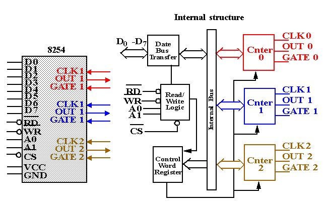
8254 Architecture
The architecture of 8254 looks as follows −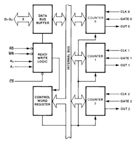
8254 Pin Description
Here is the pin diagram of 8254 −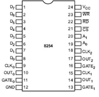
In the above figure, there are three counters, a data bus buffer, Read/Write control logic, and a control register. Each counter has two input signals - CLOCK & GATE, and one output signal - OUT.
Data Bus Buffer
It is a tri-state, bi-directional, 8-bit buffer, which is used to interface the 8253/54 to the system data bus. It has three basic functions −- Programming the modes of 8253/54.
- Loading the count registers.
- Reading the count values.

Read/Write Logic
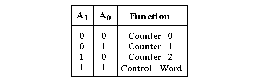
It includes 5 signals, i.e. RD, WR, CS, and the address lines A0 & A1. In the peripheral I/O mode, the RD and WR signals are connected to IOR and IOW, respectively. In the memorymapped I/O mode, these are connected to MEMR and MEMW.Address lines A0 & A1 of the CPU are connected to lines A0 and A1 of the 8253/54, and CS is tied to a decoded address. The control word register and counters are selected according to the signals on lines A0 & A1.
| A1 | A0 | Result |
|---|---|---|
| 0 | 0 | Counter 0 |
| 0 | 1 | Counter 1 |
| 1 | 0 | Counter 2 |
| 1 | 1 | Control Word Register |
| X | X | No Selection |
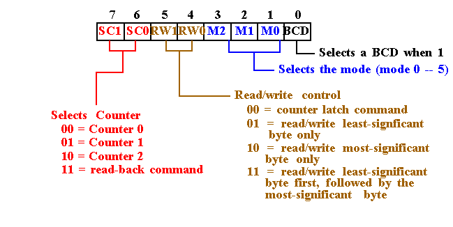
Control Word Register
This register is accessed when lines A0 & A1 are at logic 1. It is used to write a command word, which specifies the counter to be used, its mode, and either a read or write operation. Following table shows the result for various control inputs.| A1 | A0 | RD | WR | CS | Result |
|---|---|---|---|---|---|
| 0 | 0 | 1 | 0 | 0 | Write Counter 0 |
| 0 | 1 | 1 | 0 | 0 | Write Counter 1 |
| 1 | 0 | 1 | 0 | 0 | Write Counter 2 |
| 1 | 1 | 1 | 0 | 0 | Write Control Word |
| 0 | 0 | 0 | 1 | 0 | Read Counter 0 |
| 0 | 1 | 0 | 1 | 0 | Read Counter 1 |
| 1 | 0 | 0 | 1 | 0 | Read Counter 2 |
| 1 | 1 | 0 | 1 | 0 | No operation |
| X | X | 1 | 1 | 0 | No operation |
| X | X | X | X | 1 | No operation |
Counters
Each counter consists of a single, 16 bit-down counter, which can be operated in either binary or BCD. Its input and output is configured by the selection of modes stored in the control word register. The programmer can read the contents of any of the three counters without disturbing the actual count in process.Intel 8253 - Programmable Interval Timer
Q . II Intel 8253
The Intel 8253 and 8254 are Programmable Interval Timers (PITs), which perform timing and counting functions using three 16-bit counters.[1] They were primarily designed for the Intel 8080/8085-processors, but later used in x86-systems. They (or an equivalent circuit embedded in a larger chip) are found in all IBM PC compatibles. In PC compatibles, timer channel 0 is assigned to IRQ-0 (the highest priority hardware interrupt), channel 1 is assigned to DRAM refresh (at least in early models), and channel 2 is assigned to the PC speaker. The Intel 82c54 variant handles up to 10 MHz clock signals


The 8253 is described in the 1980 Intel "Component Data Catalog" publication. The 8254, described as a superset of the 8253 with higher clock speed ratings, has a "preliminary" data sheet in the 1982 Intel "Component Data Catalog". The 8254 is implemented in HMOS, has a "read back" command not available on the 8253, and permits reading and writing of the same counter to be interleaved
The timer has three counters, called channels. Each channel can be programmed to operate in one of six modes. Once programmed, the channels operate independently.[1]
There are three counters (or timers), which are labeled as "Counter 0", "Counter 1" and "Counter 2".[3] Each counter has two input pins – "CLK" (clock input) and "GATE" – and one pin, "OUT", for data output. The three counters are 16-bit down counters independent of each other, and can be easily read by the CPU.[4]
- Data bus buffer contains the logic to buffer the data bus between the microprocessor and the internal registers. It has 8 input pins, usually labelled as D7..D0, where D7 is the MSB.
- Read/write logic has 5 pins, which are listed below. The "X" denotes X is an active low signal.
- RD: read signal
- WR: write signal
- CS: chip select signal
- A0, A1: address lines
- The control word register contains the programmed information which will be sent (by the microprocessor) to the device. It defines how each channel of the PIT logically works. Each access to these ports takes about 1 µs.
The control word register contains 8 bits, labeled D7..D0 (D7 is the MSB). The decoding is somewhat complex. Most values set the parameters for one of the three counters:
- The most significant two bits (if not 11) select the counter register the command applies to.
- The next two bits (if not 00) select the format that will be used for subsequent read/write access to the counter register. This is commonly set to a mode where accesses alternate between the least-significant and most-significant bytes. One difference between the 8253 and 8254 is that the former had one internal bit which affected both reads and writes, so if the format was set to 2-byte, a read of the lsbyte would cause a following write to be directed to the msbyte. The 8254 used separate bits for reads and writes.
- The next three bits select the mode that the counter will operate in.
- The least significant bit selects whether the counter will operate in binary or BCD. (BCD counting almost never used and may not be implemented properly in emulators or southbridges.)
- Latch the count for a given timer. The next read will, rather than returning the counter value at the moment of the read, return the counter value at the moment of the latch command. After the read completes, later reads will return the current counter. When the latch command is used, the mode and BCD status are not changed.
- (8254 only) Latch the status and/or count for multiple timers. This allows multiple simultaneous latch commands using a bitmap. Also, the current channel configuration may be read back in addition to the count

When setting the PIT, the microprocessor first sends a control message, then a count message to the PIT. The counting process will start after the PIT has received these messages, and, in some cases, if it detects the rising edge from the GATE input signal. Status byte format. Bit 7 allows software to monitor the current state of the OUT pin. Bit 6 indicates when the count can be read; when this bit is 1, the counting element has not yet been loaded and cannot be read back by the processor. Bits 5 through 0 are the same as the last bits written to the control register
Operation modes
The D3, D2, and D1 bits of the control word set the operating mode of the timer. There are 6 modes in total; for modes 2 and 3, the D3 bit is ignored, so the missing modes 6 and 7 are aliases for modes 2 and 3.All modes are sensitive to the GATE input, with GATE high causing normal operation, but the effects of GATE low depend on the mode:
- Modes 0 and 4: Counting is suspended while GATE is low, and resumed while GATE is high.
- Modes 1 and 5: The rising edge of GATE starts counting. GATE may go low without affecting counting, but another rising edge will restart the count from the beginning.
- Modes 2 and 3: GATE low forces OUT high immediately (without waiting for a clock pulse) and resets the counter (on the next clock falling edge). When GATE goes high again, counting restarts from the beginning.
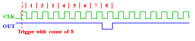
Mode 0 (000): Interrupt on terminal count
Mode 0 is used for the generation of accurate time delay under software control. In this mode, the counter will start counting from the initial COUNT value loaded into it, down to 0. Counting rate is equal to the input clock frequency.The OUT pin is set low after the Control Word is written, and counting starts one clock cycle after the COUNT is programmed. OUT remains low until the counter reaches 0, at which point OUT will be set high until the counter is reloaded or the Control Word is written. The counter wraps around to
0xFFFF internally and continues counting, but the OUT pin never changes again. The Gate signal should remain active high for normal counting. If Gate goes low, counting is suspended, and resumes when it goes high again.The first byte of the new count when loaded in the count register, stops the previous count.
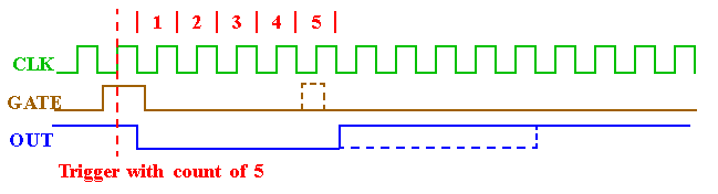
Mode 1 (001): programmable one shot
In this mode 8253 can be used as a Monostable multivibrator. GATE input is used as trigger input.OUT will be initially high. OUT will go low on the Clock pulse following a trigger to begin the one-shot pulse, and will remain low until the Counter reaches zero. OUT will then go high and remain high until the CLK pulse after the next trigger.
After writing the Control Word and initial count, the Counter is armed. A trigger results in loading the Counter and setting OUT low on the next CLK pulse, thus starting the one-shot pulse. An initial count of N will result in a one-shot pulse N CLK cycles in duration.
The one-shot is retriggerable, hence OUT will remain low for N CLK pulses after any trigger. The one-shot pulse can be repeated without rewriting the same count into the counter. GATE has no effect on OUT. If a new count is written to the Counter during a oneshot pulse, the current one-shot is not affected unless the counter is retriggered. In that case, the Counter is loaded with the new count and the oneshot pulse continues until the new count expires.
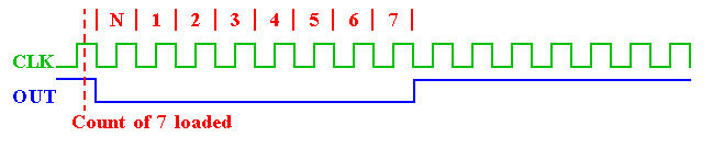
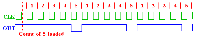
Mode 2 (X10): rate generator
In this mode, the device acts as a divide-by-n counter, which is commonly used to generate a real-time clock interrupt.Like other modes, the counting process will start the next clock cycle after COUNT is sent. OUT will then remain high until the counter reaches 1, and will go low for one clock pulse. The following cycle, the count is reloaded, OUT goes high again, and the whole process repeats itself.
The time between the high pulses depends on the preset count in the counter's register, and is calculated using the following formula:
Value to be loaded into counter =

Note that the values in the COUNT register range from to 1; the register never reaches zero.

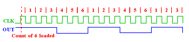
Mode 3 (X11): square wave generator
This mode is similar to mode 2. However, the duration of the high and low clock pulses of the output will be different from mode 2.Suppose is the number loaded into the counter (the COUNT message), the output will be high for counts, and low for counts. Thus, the period will be counts, and if is odd, the extra half-cycle is spent with OUT high.


Mode 4 (100): Software Triggered Strobe
After Control Word and COUNT is loaded, the output will remain high until the counter reaches zero. The counter will then generate a low pulse for 1 clock cycle (a strobe) – after that the output will become high again.GATE low suspends the count, which resumes when GATE goes high again.
Mode 5 (101): Hardware Triggered Strobe
This mode is similar to mode 4. However, the counting process is triggered by the GATE input.After receiving the Control Word and COUNT, the output will be set high. Once the device detects a rising edge on the GATE input, it will start counting. When the counter reaches 0, the output will go low for one clock cycle – after that it will become high again, to repeat the cycle on the next rising edge of GATE.
IBM PC programming tips and hints
The 8253 was used in IBM PC compatibles since their introduction in 1981.[5] In modern times, this PIT is not included as a separate chip in an x86 PC. Rather, its functionality is included as part of the motherboard chipset's southbridge. In a modern chipset, this change may show up in the form of noticeably faster access to the PIT's registers in the x86 I/O address space.All PC compatibles operate the PIT at a clock rate of 105/88 = 1.19318 MHz, 1⁄3 the NTSC colorburst frequency. This frequency, divided by 216 (the largest divisor the 8253 is capable of) produces the ≈18.2 Hz timer interrupt used in MS-DOS and related operating systems.
In the original IBM PCs, Counter 0 is used to generate a timekeeping interrupt. Counter 1 (A1=0, A0=1) is used to trigger the refresh of DRAM memory. The last counter (A1=1, A0=0) is used to generate tones via the PC speaker.
Newer motherboards include additional counters through the Advanced Configuration and Power Interface (ACPI), a counter on the Local Advanced Programmable Interrupt Controller (Local APIC), and a High Precision Event Timer. The CPU itself also provides the Time Stamp Counter (TSC) facility.
On PCs the address for timer0 (chip) is at port 40h..43h and the second timer1 (chip) is at 50h..53h.
On x86 PCs, many video card BIOS and system BIOS will reprogram the second counter for their own use. Reprogramming typically happens during video mode changes, when the video BIOS may be executed, and during system management mode and power saving state changes, when the system BIOS may be executed. This prevents any serious alternative uses of the timer's second counter on many x86 systems.
The timer that is used by the system on x86 PCs is Channel 0, and its clock ticks at a theoretical value of 1193181.8181... Hz, i.e. one third of the NTSC color subcarrier frequency, which comes from dividing the system clock (14.31818 MHz) by 12. This is a holdover of the very first CGA PCs – they derived all necessary frequencies from a single quartz crystal, and to make TV output possible, this oscillator had to run at a multiple of the NTSC color subcarrier frequency.
As stated above, Channel 0 is implemented as a counter. Typically, the initial value of the counter is set by sending bytes to the Control, then Data I/O Port registers (the value 36h sent to port 43h, then the low byte to port 40h, and port 40h again for the high byte). The counter counts down to zero, then sends a hardware interrupt (IRQ 0, INT 8) to the CPU. The counter then resets to its initial value and begins to count down again. The fastest possible interrupt frequency is a little over a half of a megahertz. The slowest possible frequency, which is also the one normally used by computers running MS-DOS or compatible operating systems, is about 18.2 Hz. Under these real mode operating systems, the BIOS accumulates the number of INT 8 calls that it receives in real mode address 0040:006c, which can be read by a program.
As a timer counts down, its value can also be read directly by reading its I/O port twice, first for the low byte, and then for the high byte. However, in free-running counter applications such as in the x86 PC, it is necessary to first write a latch command for the desired channel to the control register, so that both bytes read will belong to one and the same value.
According to a 2002 Microsoft document, "because reads from and writes to this hardware [8254] require communication through an IO port, programming it takes several cycles, which is prohibitively expensive for the OS. Because of this, the aperiodic functionality is not used in practice."
| Short Description | ||||||||
|---|---|---|---|---|---|---|---|---|
| D7 SC1 | D6 SC2 | D5 RW1 | D4 RW0 | D3 M2 | D2 M1 | D1 M9 | D0 BCD | |
| 0 | 0 | format | mode | BCD | Set mode of Counter 0 | |||
| 0 | 1 | format | mode | BCD | Set mode of Counter 1 | |||
| 1 | 0 | format | mode | BCD | Set mode of Counter 2 (at port 42h) | |||
| 1 | 1 | count | status | C2 | C1 | C0 | x | Read-back command (8254 only) |
| counter | 0 | 0 | — x — | Latch counter value. Next read of counter will read snapshot of value. | ||||
| counter | 0 | 1 | mode | BCD | Read/Write bits 0..7 of counter value | |||
| counter | 1 | 0 | mode | BCD | Read/Write bits 8..15 of counter value | |||
| counter | 1 | 1 | mode | BCD | 2xRead/2xWrite bits 0..7 then 8..15 of counter value | |||
| counter | format | 0 | 0 | 0 | BCD | Mode 0: Interrupt on Terminal Count | ||
| counter | format | 0 | 0 | 1 | BCD | Mode 1: Hardware Retriggerable One-Shot | ||
| counter | format | x | 1 | 0 | BCD | Mode 2: Rate Generator | ||
| counter | format | x | 1 | 1 | BCD | Mode 3: Square Wave | ||
| counter | format | 1 | 0 | 0 | BCD | Mode 4: Software Triggered Strobe | ||
| counter | format | 1 | 0 | 1 | BCD | Mode 5: Hardware Triggered Strobe (Retriggerable) | ||
| counter | format | mode | 0 | Counter is a 16-bit binary counter(0–65535) | ||||
| counter | format | mode | 1 | Counter is a 4-digit binary coded decimal counter (0–9999) | ||||
| 1 | 1 | count | status | C2 | C1 | C0 | x | Read-back command (8254 only) |
| 1 | 1 | 0 | 0 | C2 | C1 | C0 | x | Next read of selected counters will read back latched status, then count. |
| 1 | 1 | 0 | 1 | C2 | C1 | C0 | x | Next read of selected counters will read back latched count. |
| 1 | 1 | 1 | 0 | C2 | C1 | C0 | x | Next read of selected counters will read back latched status. |
| 1 | 1 | 1 | 1 | C2 | C1 | C0 | x | Do nothing (latch nothing on any or all counters) |
| 1 | 1 | count | status | 0 | 0 | 0 | x | Do nothing (latch count and/or status on no counters) |
| 1 | 1 | count | status | 1 | C1 | C0 | x | Read-back command applies to counter 2 |
| 1 | 1 | count | status | C2 | 1 | C0 | x | Read-back command applies to counter 1 |
| 1 | 1 | count | status | C2 | C1 | 1 | x | Read-back command applies to counter 0 |
| Bit #/Name | Short Description | |||||||
|---|---|---|---|---|---|---|---|---|
| D7 Output Status | D6 null count | D5 RW1 | D4 RW0 | D3 M2 | D2 M1 | D1 M0 | D0 BCD | |
| 0 | X | X | X | X | X | X | X | Out pin is 0 |
| 1 | X | X | X | X | X | X | X | Out pin is 1 |
| X | 0 | X | X | X | X | X | X | Counter can be read |
| X | 1 | X | X | X | X | X | X | The counter is being set |
| X | X | = | = | = | = | = | = | As defined for the control word register |
Q . IIII Electronic Timers
An Eagle Signal electronic timer would be the timer of choice when fast, high precision accuracy and event feedback are required.
An electronic timer is more compact and also more complex than electro-mechanical timers. If feedback/output control functions are required (in terms of an alarm or another pre-programmed event), an electronic timer is a better fit than an electro-mechanical timer. Each electronic timer offers digital programmability. Some models have a choice of LED or LCD display. Some also operate as multifunction devices and others with long time ranges. These programmable timer solutions are available in many forms to meet many different needs: time indicators, reset timers, repeat cycle timers and multifunction timers. Electronic timer models can be more complex yet remain rugged and require minimal maintenance.


Microprocessors Questions and Answers – Programmable Interval Timer 8254
This set of Microprocessor Multiple Choice Questions & Answers (MCQs) focuses on “Programmable Interval Timer 8254”.
1. The number of counters that are present in the programmable timer device 8254 is
a) 1
b) 2
c) 3
d) 4
View Answer
a) read operation
b) write operation
c) read and write operations
d) none
View Answer
a) mode 0
b) mode 1
c) mode 2
d) mode 3
View Answer
a) 1 clockcycle
b) 2 clockcycles
c) 3 clockcycles
d) 4 clockcycles
View Answer
a) mode 1
b) mode 2
c) mode 3
d) mode 4
View Answer
a) counter 0
b) counter 1
c) counter 2
d) none
View Answer
a) read/load least significant byte only
b) read/load most significant byte only
c) read/load LSB first and then MSB
d) read/load MSB first and then LSB
View Answer
a) decimal count
b) hexadecimal count
c) binary count
d) octal count
View Answer
a) GATE signal is low
b) GATE signal is high
c) CLK signal is low
d) CLK signal is high
View Answer
a) initialising the operating modes
b) selection of counters
c) choosing binary/BCD counters
d) all of the mentioned
View Answer
1. The number of counters that are present in the programmable timer device 8254 is
a) 1
b) 2
c) 3
d) 4
View Answer
Answer: c
Explanation: There are three counters that can be used as either counters or delay generators.
2. The operation that can be performed on control word register isExplanation: There are three counters that can be used as either counters or delay generators.
a) read operation
b) write operation
c) read and write operations
d) none
View Answer
Answer: b
Explanation: The control word register can only be written and cannot be read.
3. The mode that is used to interrupt the processor by setting a suitable terminal count isExplanation: The control word register can only be written and cannot be read.
a) mode 0
b) mode 1
c) mode 2
d) mode 3
View Answer
Answer: a
Explanation: Mode 0 is also called as interrupt on terminal count.
4. In mode 2, if N is loaded as the count value, then after (N-1) cycles, the output becomes low forExplanation: Mode 0 is also called as interrupt on terminal count.
a) 1 clockcycle
b) 2 clockcycles
c) 3 clockcycles
d) 4 clockcycles
View Answer
Answer: a
Explanation: After (N-1) cycles, the output becomes low for only 1 clockcycle. If the count N is reloaded and again the output becomes high and remains so for (N-1) clock pulses.
5. The generation of square wave is possible in the modeExplanation: After (N-1) cycles, the output becomes low for only 1 clockcycle. If the count N is reloaded and again the output becomes high and remains so for (N-1) clock pulses.
a) mode 1
b) mode 2
c) mode 3
d) mode 4
View Answer
Answer: c
Explanation: When the count N loaded is even, then for half of the count, the output remains high and for the remaining half it remains low. If the count loaded is odd, the first clock pulse decrements it by 1 resulting in an even count value.
6. In control word register, if SC1=0 and SC0=1, then the counter selected isExplanation: When the count N loaded is even, then for half of the count, the output remains high and for the remaining half it remains low. If the count loaded is odd, the first clock pulse decrements it by 1 resulting in an even count value.
a) counter 0
b) counter 1
c) counter 2
d) none
View Answer
Answer: b
Explanation: SC denotes select counter.
7. In control word format, if RL1=1, RL0=1 then the operation performed isExplanation: SC denotes select counter.
a) read/load least significant byte only
b) read/load most significant byte only
c) read/load LSB first and then MSB
d) read/load MSB first and then LSB
View Answer
Answer: c
Explanation: To access 16 bit, first LSB is loaded first, and then MSB.
8. If BCD=0, then the operation isExplanation: To access 16 bit, first LSB is loaded first, and then MSB.
a) decimal count
b) hexadecimal count
c) binary count
d) octal count
View Answer
Answer: b
Explanation: If BCD=0 then hexadecimal count. If BCD=1, then the operation is BCD count.
9. The counter starts counting only ifExplanation: If BCD=0 then hexadecimal count. If BCD=1, then the operation is BCD count.
a) GATE signal is low
b) GATE signal is high
c) CLK signal is low
d) CLK signal is high
View Answer
Answer: b
Explanation: If the GATE signal is enabled, then the counter starts counting.
10. The control word register contents are used forExplanation: If the GATE signal is enabled, then the counter starts counting.
a) initialising the operating modes
b) selection of counters
c) choosing binary/BCD counters
d) all of the mentioned
View Answer
Answer: d
Explanation: The control word register contents are used for
i) initialising the operating modes (mode 0-mode 4)
ii) selection of counters (counter0-counter2)
iii) choosing binary or BCD counters
iv) loading of the counter registers
Explanation: The control word register contents are used for
i) initialising the operating modes (mode 0-mode 4)
ii) selection of counters (counter0-counter2)
iii) choosing binary or BCD counters
iv) loading of the counter registers
8254 Programmable Timer is used for timing control applications in microcomputer systems. The design is capable of generating accurate time delays under software control.
")
Q . IIIII 8253 functions
| General The Intel 8253 is a programmable counter / timer chip designed for use as an Intel microcomputer peripheral. It uses nMOS technology with a single +5V supply and is packaged in a 24-pin plastic DIP. It is organized as 3 independent 16-bit counters, each with a counter rate up to 2 MHz. All modes of operation are software programmable. The 82C54 is pin compatible with the HMOS 8254, and is a superset of the 8253. Six programmable timer modes allow the 82C54 / 8253 to be used as an event counter, elapsed time indicator, programmable one-shot, and in many other applications. | |||||||||||||||||||||||||||||||||||||||||||||||||||||||||||||||||||||||||||||||||||||||||||||||||
| Block diagram I'll examine the block diagram and next I'll explore the internal registers and operating modes of this device. Take note, the timer has three independent, programmable counters and they are all identical.
| |||||||||||||||||||||||||||||||||||||||||||||||||||||||||||||||||||||||||||||||||||||||||||||||||
| PIN configuration The following picture shows the pin configuration of the 8253 and a general definition of the lines follows:
| |||||||||||||||||||||||||||||||||||||||||||||||||||||||||||||||||||||||||||||||||||||||||||||||||
| Internal 8253 registers Here is a list of the internal 8253 registers that will program the internal counters of the 8253:
| |||||||||||||||||||||||||||||||||||||||||||||||||||||||||||||||||||||||||||||||||||||||||||||||||
Control Word Register
The 1st value, $00, is the counter latch mode. If this mode is specified, the current counter value is latched into an internal register at the time of the I/O write operation to the control register. When a read of the counter occurs, it is this latched value that is read. Caution: If the latch mode is not used, then it is possible that the data read back may be in the process of changing while the read is occurring. This could result in invalid data being input by the CPU ( see the timing diagrams to the 8253 by intel's site or go to page "Memory mapped I/O" ). To read the counter value while the counter is still in the process of counting, one must first issue a latch control word, and then issue another control word that indicates the order of the bytes to be read. An alternative method of obtaining a stable count from the timer is to externally inhibit counting while the register is being read. To this, an external logic to the 8253 controlled by the Z80 to inhibit count during an input read operation is to connect. Each technique has certain disadvantages. The first, the latching method, may give the CPU a reading that is "old" by several cycles, depending on the speed of the count and which byte of the counter is being read. The second method, the external inhibiting function, requires additional hardware. In addition, it may change the overall system operation. The counters 1 and 2 of the MZ-700 are not designed with this additional hardware function. :-( but the counter 0. You can use this method for your own purposes even an amplifier is connected to the output pin of this counter. The next 3 bits of the control word are D3, D2, and D1. These bits determine the basic mode of operation for the selected counter. The mode descriptions follows:
| |||||||||||||||||||||||||||||||||||||||||||||||||||||||||||||||||||||||||||||||||||||||||||||||||
| Modes The following text describes all possible modes. The modes used in the MZ-700 and set by the monitor's startup are mode 0, mode 2, and mode 3.
| |||||||||||||||||||||||||||||||||||||||||||||||||||||||||||||||||||||||||||||||||||||||||||||||||


Memory mapped I/O
( Executing I/O operations by storage address)
|
The ports from $E000 to $E008 are allocated to these functions and chips:
|
Q . IIIIIII 80186 Microprocessors with Integrated Peripherals: Introduction and Architecture
The Intel 80186 is an improved version of the 8086 microprocessors. 80186 is a 16-bit microprocessor with 16- bit data bus and 20-bit address bus.
It has a programmable peripheral devices integrated in the same package. The instruction set of the 80186 is a superset of the instruction set of the 8086. The term superset means that all of the 8086 instructions will execute properly on an 80186, but the 80186 having the few additional instructions. We will see on Instruction set of 80186 under this heading.
Following figure shows the block diagram and pin diagram of 80186. The CPU is divided into seven independent functional parts.
 |
| 80186 internal block diagram |
 |
| 80186 68-pins pin diagram |
1. The Bus Interface Unit (BIU)
2. Execution Unit (EU)
3. Clock Generator
4. Programmable interrupt controller
5. Programmable Chip Select Unit (CSU)
6. Programmable DMA Unit
7. Programmable counter/timers
The 80186 has the same bus interface unit (BIU) and execution unit (EU) as the 8086. We can see this under the heading The 8086 Microprocessor- Internal Architecture. The 80186 is 68 pins leadless package, so it has enough pins to send out both the minimum mode type signals \[\overline{RD}\] and \[\overline{WR}\] and the S0 – S3 status signals which can be connected to external bus controller ICs for maximum mode systems. It does not have a pin labeled \[MN/\overline{MX}\] for switching minimum mode through maximum mode.
Clock Generator:
The 80186 has the built in clock generator so that we can add external crystal. This reduces the component count in a system. It has three pin connections: X1, X2, and CLKOUT. The X1 and X2 pins are connected to a crystal that resonate twice the operating frequency of the microprocessor. The CLKOUT pin provides a system clock signal that is one-half the crystal frequency. In addition to external pins, the clock generator provides the internal timing for synchronizing the READY input pin.
Programmable Interrupt Controller:
Programmable interrupt controller has four interrupt input: INT0, INT1, \[INT2/\overline{INTA0}\] and \[INT3/\overline{INTA1}\] as well as one nonmaskable interrupt NMI input. These inputs operates with two modes : internal mode and external mode. In internal mode, if the four INT inputs are programmed, then a signal applied to one of them to push the return address on the stack and vector directly to the start of the interrupt service procedure for that interrupt. In external mode, the \[INT2/\overline{INTA0}\] and \[INT3/\overline{INTA1}\] pins can be programmed to be used as interrupt inputs or they can be programmed to function as interrupt acknowledge outputs. This mode is used to interface with external 8259As. When the 8259A is externally attached with 80186, 80186 microprocessors works as the master and the 8259A works as the slave.
Programmable Chip Select Unit:
This built in address decoder unit can be programmed to produce an active low chip select signal when the memory or port address in a specified range is sent out. This built-in decoder is to select major blocks of memory. six memory address chip select signals are available: lower chip select lines \[\overline{LCS},\] upper chip select lines \[\overline{UCS},\] and middle chip select lines \[\overline{MCS0}-3.\] The boundary of the lower chip select signal is begins at location 00000H and the boundary of the upper chip select signal is ends at location FFFFFH. The sizes of the memory areas are programmable by some bits put in a control word, and wait states (0-3 waits) can be automatically inserted with the selection of an area of memory.
In addition to producing memory chip select signals, the 80186 can be programmed to produce up to seven peripheral chip select signals on its \[\overline{PCS0}-\overline{PCS4},\] \[\overline{PCS5}/A1,\] and \[\overline{PCS6}/A2\] pins. The programmable I/O area starts at a base I/O address programmed by the user, and all seven 128-byte blocks are contiguous.
Programmable DMA Unit:
The DMA unit has two DMA request inputs, DRQ0 and DRQ1. These inputs allow external devices such as disk controllers, CRT controllers etc. to request use of one of the DMA channels. For each DMA channel the 80186 has a full 20-bit register to hold the source address, a 20-bit register to hold the destination address, and a 16-bit counter to keep track of how many words or bytes have been transferred. DMA transfers can be from memory to memory, I/O to I/O, or between I/O and memory.
Programmable counter/timers:
The timer section contains three fully programmable 16-bit timers. Timers 0 and 1 generate waveforms for external use, and are driven by either the master clock of 80186 or by an external clock. They are also used to count external events. The third timer, timer 2, is internally connected to the processor clock. The output of timer 2 generates an interrupt after a specified number of clocks and can provide a clock to the other timers.
Q . IIIIIII Classification of Computer
The way computers process the information can be broadly classified into three categories.
 |
| Classification of Computer |
1. Analog Computers
In analog computers, continuous quantities are used. Computations are carried out with physical quantities such as voltage, length, current, temperature etc. For ex: Voltmeter, ammeter, thermometer. These computers operate by measuring rather than counting. All calculations are parallel and faster.
2. Digital Computers
The digital computers work upon discontinuous data. They convert the data into digit (binary digit 0 and 1) and all operations carried out at fast rates. Computers used for business and scientific applications are digital computers. They can be further classified into 2 ways
- Purpose wise
- Size and performance wise
i. Purpose wise Computers
Purpose wise digital computers are classified into two types:
· Special Purpose Computers
o These computers were designed to perform a specific task. The instructions carried out the tasks are permanently stored in the machine. For the specific tasks, this type of computer works efficiently but such computers are not versatile.
o Ex: Blood pressure monitoring system
· General purpose Computers
o This type of computers can work on different types of programs input to it and thus be used in countless applications. The programs are not permanently stored but are input at the time of execution. These computers are versatile.
ii. Size and performance wise
Size and performance wise computers can be classified into 4 types:
a) Microcomputers
These computers are also known as PC’s. PC’s are single processor systems which can perform simple task such as word processing, spreadsheet calculations or graphics rendering. The first PC was built by IBM.
b) Minicomputers
This type of computers usually designed for real time dedicated applications or as high performance, multiple user applications. Today’s minicomputers are the multiprocessor systems running on UNIX operating system.
Ex: Digital Alpha, IBM RS/6000, Sun Ultra.
c) Mainframes
Applications which require high performance or generate and process large number of transaction are generally use mainframes. These computers generally used by banks to process ATM, check and electronic transactions.
Ex: S/390
d) Supercomputers
These computers are designed for ultra high performance tasks such as weather analysis, encryption cracking and creation of animation. Supercomputers are large in size and more expensive. These computers are owned by govt. agencies and large corporations. National Security Agency(NSA) houses use this computers for code breaking and intelligence gathering.
Ex: IBM’s Deep Blue.
e) Workstation
The term workstation has two meanings.
1. It can simply refer to an ordinary personal computer that is connected to a network.
2. It is a powerful desktop computers used for high performance tasks, such aas medical imaging and computer Aides Design, that require a lot of processing speed.
3. Some workstation contains more than one microprocessor.
4. Cost of a workstation is more than an average personal computer.
3. Hybrid Computers
Hybrid computers utilize the best qualities of both the digital and analog computers. Some calculation take place in analog manner and rest of them take place in digital manner. These computers are generally used in hospitals to measure patients heart beat, blood pressure, temperature and other vital signals. Hybrid computers are also used in weather forecasting.
Q . IIIIIIII The Unguided Transmission (Wireless): Infrared and Millimeter Waves
Infrared and millimeter waves are widely used for short-range communication. The remote controls used on televisions, VCR’s, and stereos all use infrared communication.
They are relatively directional, cheap, and easy to build, but they cannot pass through solid objects.
It can be used for indoor wireless LANs; without any interfere with a similar system in adjacent rooms i.e. security is better than radio systems.
It cannot be used outdoors because the sun shines as brightly in the infrared as in the visible spectrum.
Electronic timer switch with time tracker
A programmable timer for turning a light on and off in response to changing sunset, daylight savings time, and other programmable conditions. The programmable timer includes an input device, a microprocessor, and a switch. The input device provides calendar, geographical, and daylight savings information to the microprocessor, which stores the programming information. The microprocessor computes an effective switching time from the stored information. The microprocessor employs program logic that compares the effective switching time to the current time to generate a timing control signal. The timing control signal, in turn, causes the switch to turn a light on and off. In the preferred embodiment, the microprocessor and the switch are included within a housing which mounts on a wall in place of a normal light switch. A liquid crystal display is disposed on a face of the housing to provide a read out of the programming information and of the time of day. The input device is disposed on the face of the housing and includes a key matrix having a plurality of finger settable key type programming switches. Information is programmed by depressing each key while the programming logic is in a particular program mode.
Q . IIIIIIIIII Cache Memory
We have already discussed about the Primary memory and Secondary memory. Also seen the difference between SRAM static RAM and DRAM: Dynamic RAM. Today in this post we will discuss the cache memory.
The cache is a small amount of high-speed memory, present between the primary memory (RAM) and CPU (processor). Its access time is much less compared to that of the main memory. It is an intermediate memory and is not accessible to users. It stores instructions and data, which are to be immediately executed. It is used to reduce the average access time reading data, which are stored in main memory. Thus the cash memory increases the operating speed of the system. But it is mush costlier than main memory. There are two levels of cache memory
L1 and L2, L1 cache memory will present inside CPU, where as the L2 cache will be present on the mother board. L1 cache is very fast since it runs at a speed of processor. L2 cache is larger but slower in speed than L1 cache.
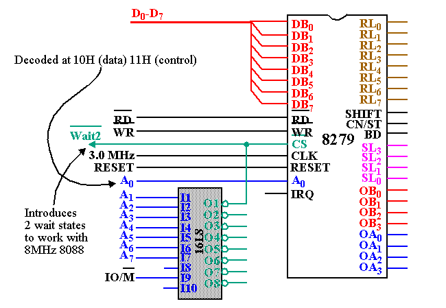
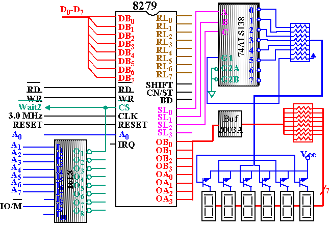
Q . IIIIIIIIIII Programmable Keyboard/Display Interface - 8279
Programmable Keyboard/Display Interface - 8279
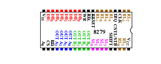
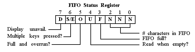
Pinout Definition 8279
- A0: Selects data (0) or control/status (1) for reads and writes between micro and 8279.
- BD: Output that blanks the displays.
- CLK: Used internally for timing. Max is 3 MHz.
- CN/ST: Control/strobe, connected to the control key on the keyboard.
- CS: Chip select that enables programming, reading the keyboard, etc.
- DB7-DB0: Consists of bidirectional pins that connect to data bus on micro.
- IRQ: Interrupt request, becomes 1 when a key is pressed, data is available.
- OUT A3-A0/B3-B0: Outputs that sends data to the most significant/least significant nibble of display.
- RD(WR): Connects to micro's IORC or RD signal, reads data/status registers.
- RESET: Connects to system RESET.
- RL7-RL0: Return lines are inputs used to sense key depression in the keyboard matrix.
- Shift: Shift connects to Shift key on keyboard.
- SL3-SL0: Scan line outputs scan both the keyboard and displays.
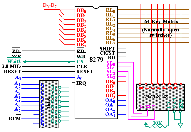
Keyboard Interface of 8279
Interface of 8279
- 1010WWBB
- The display write inhibit control word inhibits writing to either the leftmost 4 bits of the display (left W) or rightmost 4 bits.
- BB works similarly except that they blank (turn off) half of the output pins.
- 1100CCFA
- The clear control word clears the display, FIFO or both
- Bit F clears FIFO and the display RAM status, and sets address pointer to 000.
- 1110E000
Interface of 8279
Programmable Interval Timer: 8254
- Used for controlling real-time events such as real-time clock, events counter, and motor speed and direction control.
8254 Pin Definitions
- CLK: The clock input is the timing source for each of the internal counters.
- CS: Chip Select enables the 8254 for programming, and reading and writing.
- G: The gate input controls the operation of the counter in some modes.
- OUT: A counter output is where the wave-form generated by the timer is available.
- RD/WR: Read/Write causes data to be read/written from the 8254 and often connects to the IORC/IOWC.
8254 Programming
- The control word allows the programmer to select the counter, model of operation, binary or BCD count and type of operation (read/write).
8254 Programming

=== MICRO 520 MA THE COM STATUE PROCESS MATIC ===
I just want to thank you for sharing your information and your site or blog this is simple but nice Information I’ve ever seen i like it i learn something today. Building inspection
BalasHapus