Electronic and Computer Engineering IN transfer memo changing world AMNIMARJESLOW GOVERNMENT 91220017 LOR INTEL EL ACCU EL APP RESEARCH 02096010014 ELCLEAR LJBUSAF ADAPTER TRANSFER XGIGO XWAM PROCESS !
Computers are all pervasive. Almost every aspect of daily life from shopping in a supermarket to flying abroad depends on highly sophisticated computing systems.
The challenges in designing and delivering effective, safe and cost efficient systems require a complex integration of application knowledge, software and electronics, interfaced to a rapidly changing world.
With continuing advancing technologies as like as the research of intelligent video processing technology, internet of things and human-computer interaction.
the basic foundation of computer electronics begins with an elementary approach called accumulator through the input process ---- memory ---- process ----- output --@ X . I Accumulator Accumulator is a very important register for operations in microprocessor. It is used as source of one of the operands to the Arithmetic and Logic Unit (ALU). It is also the destination of the result. The size of the accumulator is the same as the word size of the microprocessor. It is usually represented by a symbol, A.
A microprocessor that uses accumulator for storing data is called accumulator based microprocessor. Usually 8-bit microprocessors are accumulator based. Some of these microprocessors are Intel 8085 and Motorola 6809.
In 16-bit and 32-bit microprocessors the accumulator is replaced by a general purpose register. These microprocessors are called general purpose register based microprocessors. Some of these microprocessors are Intel Pentium and Motorola 68000/68020. When a microprocessor contains many general purpose registers, any one of them can be used as an accumulator.
Registers In Microprocessor
What is register?
Register is a small high speed named memory. It consists of a set of binary storage cells called flip-flops with parallel reading or writing or both the facilities. The number of bits in a register depends on the type and address of the data.
Register plays a major role in CPU operations. Microprocessor picks up data from one of the registers for doing arithmetic or logical operation. Once the operation is over, it stores the result in a register. Data are usually loaded from memory to register. Similarly the resultant data will be loaded from registers to memory.
The first microprocessor was introduced in 1971 by Intel Corp. It was named Intel 4004 as it was a 4 bit processor. It was a processor on a single chip. It could perform simple arithmetic and logic operations such as addition, subtraction, boolean AND and boolean OR. It had a control unit capable of performing control functions like fetching an instruction from memory, decoding it, and generating control pulses to execute it. It was able to operate on 4 bits of data at a time.This first microprocessor was quite a success in industry. Soon other microprocessors were also introduced. Intel introduced the enhanced version of 4004, the 4040. Some other 4 bit processors are International’s PPS4 and Thoshiba’s T3472.
8-bit Microprocessors
The first 8 bit microprocessor which could perform arithmetic and logic operations on 8 bit words was introduced in 1973 again by Intel. This was Intel 8008 and was later followed by an improved version, Intel 8088. Some other 8 bit processors are Zilog-80 and Motorola M6800.
16-bit Microprocessors
The 8-bit processors were followed by 16 bit processors. They are Intel 8086 and 80286.
32-bit Microprocessors
The 32 bit microprocessors were introduced by several companies but the most popular one is Intel 80386.
Pentium Series
Instead of 80586, Intel came out with a new processor namely Pentium processor. Its performance is closer to RISC performance. Pentium was followed by Pentium Pro CPU. Pentium Pro allows allow multiple CPUs in a single system in order to achive multiprocessing. The MMX extension was added to Pentium Pro and the result was Pentiuum II. The low cost version of Pentium II is celeron.
The Pentium III provided high performance floating point operations for certain types of computations by using the SIMD extensions to the instruction set. These new instructions makes the Pentium III faster than high-end RISC CPUs.
Interestingly Pentium IV could not execute code faster than the Pentium III when running at the same clock frequency. So Pentium IV had to speed up by executing at a much higher clock frequency.
General Purpose Registers
General purpose registers (GPR) are not used for storing any specific type of information. Instead operands as well as addresses are stored at the time of program execution. However the operand and the address information may not be of the same size. For example, in 8-bit microprocessors, the data is 8 bit whereas the address is 16 bit.
To allow storage of both types of information, provision is usually made to access registers individually with bit size, say, k or as register pairs where the registers are concatenated to provide bit size of 2 k as shown in the following figure.
General Purpose Register
Addressing Mode
What is Addressing Mode?
In any microprocessor instruction, the source and the destination can be a register, memory content or an 8 bit number. In fact, these source and destination are operands. The various forms of specifying the operands are called the addressing mode.
Four types of addressing modes are explained in this article.
1. Immediate Addressing 2. Register Addressing 3. Direct Addressing 4. Indirect Addressing
1. Immediate Addressing
In immediate addressing mode, the operand is readily available with the instruction. For example, in the following instruction, MVI A, 05 The data, 05 is moving to accumulator.
2. Register Addressing
In this mode, operand is in any one of the general purpose register. So, the name of the register is given as operand. For example, in the following instruction, MOV A, B The data contained in the register, B is moving to accumulator, A.
3. Direct Addressing
In this mode, the operand is available in the memory. So, the address of the memory location should be given as operand. Normally, these types of instructions will have 3 bytes. Consider the following instruction, LDA 2050 It load the content of the memory location, 2050 to accumulator. Note that here the operand is indicated by its address.
4. Indirect Addressing
In this mode, the operand is available in memory but its address is indicated by any one of the register pair. Normally, the address is indicated by the HL (two parts of memory address) pair of memory. The name of the register pair is given as operand. Hence it is indirect. MOV A, M In the above instruction, M refers to HL pair. It moves the content of the memory location indicated by HL pair to accumulator.
The following instruction, LDAX B move the content of the memory location indicated by the register pair, BC.
Arithmetic And Logic Unit
Arithmetic and Logic Unit (ALU) in microprocessor is capable of performing the following operations on binary data.
Binary addition and subtraction
Logical AND, OR, XOR
Complement
Rotate left and right
ALU has three registers: accumulator, temporary register and flag register (SR). Accumulator and temporary register are used to hold the operand of the operations being performed. The result of the operation is again placed in the accumulator replacing all the existing original operands.
The ALU contains number of flip-flops called flags to store information related to the result of the operation. The information may be sign of the result, carry status, result is 0 or not, parity etc. Decimal adjust is an additional unit used to adjust the result of the addition operation.
Control Unit The control unit controls and synchronizes all the data transfer in microprocessor system. The control unit uses inputs from a master clock to drive timing and control signals that regulate the data transfer in the system associated with each instruction. It also accepts the control signals generated by other devices in the microprocessor system which alters the state of the microprocessor. Control unit regulate the instruction cycle
Embedded Microprocessor
What is embedded microprocessor?
Embedded microprocessors are embedded inside other devices. Usually these processors are used as microcontrollers in devices such as automotive ignition control, digital radio tuning, printers, mobile phones, DVD players and washing machines. The functions of microcontrollers were once done by mechanical devices. Generally embedded microprocessors are 8 bit devices programmed in assembly language.
Nowadays RISC microcontrollers such as ARM used as they are cheap and consume low power. Moreover the software can be written in high level languages such C, C++ and Java. This allows easy coding in less time.
Embedded System
An embedded system is a microprocessor-based system that controls a function or set of functions. A typical embedded systems consists of the following components: processor, memory, peripherals and software.
Advantages
Microprocessors that are used as embedded controllers are cheap
More efficient than mechanical devices
Ease of design
Software portability
Replacement of analog circuits
High noise immunity
Self-test features
No component ageing and drift
Applications of Microprocessor
The wide range of application area of the microprocessor can be broadly classified into two groups: general purpose application and special purpose application.
1. General purpose application
i) Single board micro computers
Single board microcomputers are simple and cheaper. They have the minimum possible software and hardware configuration. They are used to train the students. They are also used to build small computer based systems.
ii) Personal Computers
The home computer made up of a 8 bit microprocessor are used for playing video games and learning simple programs. The 16 bit computers are used for word processing, payroll, business accounts, etc.
iii) Super Minis and CAD
32 bit processors are used to build powerful microcomputers. Their performance is better than mainframe and mini-computers. These systems are used in Engineering side as computer aided design machines.
2. Special purpose application.
i) Instrumentation
The microprocessor based instrument can be made intelligent using feature programmability. Microprocessors can be used as controllers in various instruments. They are also used in medical instruments to measure blood pressure and temperature.
ii) Control
Microprocessor controllers are now available in home appliances such as microwave oven, washing machine. In industry, microprocessors are used in controlling various process parameters such as speed, temperature, moisture and pressure.
iii) Communication
In the telephone industry, microprocessors are used in digital telephone sets, telephone exchanges and modems. They are also used in railway reservation system at the national level and air reservation system at international level. Satellite communication systems, mobile phones and televisions are also using microprocessors.
iv) Office Automation and Publication
With the availability of inexpensive and user friendly microcomputers along with wide range of software packages, office works are computerized. Microcomputers are used in office to perform word processing, spreadsheet operations, storage and retrieval of huge information. In publishing houses microprocessor based systems are used for making automatic photo copies. Microprocessor based LASER printers are used to achieve good speed in printing.
Each instruction has two parts: one is the task to be performed called the operation code (opcode) and the other is the data to be operated on called the operand (data).
Instruction And Word Size
1. One word or one byte Instruction
It includes the opcode and operand in the same byte. Example:ADD B
2. Two word or two byte Instruction
First byte specifies the opcode and second byte specifies the operand. Example:MVI A, 05
3. Three word or three byte Instruction
The first byte specifies the opcode and the following two bytes specify the 16 bit address. The second byte is lower order and the other is higher order. Example:JMP 2085H X . II Basic computer design and accumulator logic
Hardware Component of BC

A memory unit:4096x16.
Registers: AR,PC,DR,AC,IR,TR,OUTR,INPR,and SC
Flip-Flops(Status): I,S,E,R,IEN,FGI,and FGO
Decoders: A 3x8 Opcode decoder A 4x16 timing decoder
Common bus:16bits
Control logic gates
Adder and Logic circuit :Connected to AC


Control Logic Gates

inputs:


Two decoder outputs
I flip-flop
IR (0-11)
AC(0-15): To check if AC=0 and To detect sign bit AC(15)
DR(0-15):To check if DR=0
Values of seven flip-flops

Outputs:


Input Controls of the nine registers
Read and Write Controls of memory
Set ,Clear, or Complement Controls of the flip-flops
S2,S1,S0 Controls to select a register for the bus
AC ,and Adder and Logic circuit


Control of Register and Memory
The control inputs of the registers are LD (load), INR(increment) and CLR (clear).


Address Register
To derive the gate structure associated with the control inputs of AR: we find all the statements that change the contents of AR.

fig. control gates associated with AR


Similarly,control gates for the other registers , as well as the read and write inputs of memory can be derived . The logic gates associated with the read inputs of memory is derived by scanning all statements that contain a read operation. (Read operation is recognized by the symbol <--M[AR]).

..


The output of the logic gates that implement the Boolean expression above must be connected to the read input of memory.


Control fo flip-flop
The control gates for the seven flip-flops can be determined in a similar manner.

Example:


Interrupt Enable Flag(IEF)
IEF instruction


These three instructions can cause IEN flag to change its value.

fig.control input for IEN


Control of Common Bus
The16 bit common bus is controlled by the selection inputs S2, S1 and S0. Binary numbers for S2S1S0 is associated with a Boolean variablex1 throughx7,which must be active in order to select the register or memory for the bus.

fig.Encoder for Bus Selection Circuit


Example:whenx1=1,S2S1S0 must be 001 and thus output of AR will be selected for the bus.

To determine the logic for each encoder input, it is necessary to find the control functions that place the corresponding register onto the bus.

Example: to find the logic that makesx1 =1, we scan all register transfer statements that have AR as a source.

..


Therefore, the Boolean function for x1 is,

.


Similarly, for memory read operation,

.


fig. Encoder for bus selection inputs


Design of Accumulator Logic
To design the logic associated with AC, we extract all register transfer statements that change the contents of AC. The circuit associated with the AC register is shown below:

fig.circuit associated with AC


instruction sample In AC


Control of AC Register
The gate structure that controls the LD, INR and CLR inputs of AC is shown below:

fig.Gate structure for controlling LD, INR and CLR of AC


Adder and Logic Circuit
fig.One stage of adder and logic circuit


The adder and logic circuit can be sub-divided into 16 stages, with each bit corresponding to one bit of AC.


One stage of the adder and logic circuit consists of seven AND gates,one OR gate and a full adder (FA) as shown above.
The input is labelled Ii output AC(i).
When LD input is enabled, the 16 inputs Ii for i=0,1,2…15 are transferred to AC(i).
The AND operation is achieved by ANDing AC(i) with the corresponding bit in DR(i).
The transfer from INPR to AC is only for bits 0 through 7.
The complement microoperation is obtained by inverting the bit value in AC.
Shift-right operation transfers bit from AC(i+1) and shift-left operation transfers the bit from AC(i-1).
Hardware components consists of memory unit, registers, flip-flop, decoders, common bus, control logic gates and adder and logic circuit
The control inputs of the resisters are LD (load), INR (increment) and CLR (clear).
To determine the logic for each encoder input, it is necessary to find the control functions that place the corresponding register onto the bus.
The 16 bit common bus is controlled by the selection inputs S2, S1 and S0. Binary numbers for S2S1S0 is associated with a Boolean variable x1 through x7, which must be active in order to select the register or memory for the bus.
To design the logic associated with AC, we extract all register transfer statements that change the contents of AC.
Instrumentation control example with electronic computer ! A household electric heater serves as a simple example of process control
Memory provides permanent storage to the operating system for data used by the CPU. The system’s read-only memory (ROM) stores data permanently for the operating system random access memory (RAM) stores status information for input and output devices, along with values for timers, counters, and internal devices. PLCs require a programming device, either a computer or console, to upload data onto the CPU.

3. A CPU operating cycle includes the following steps: a) start        scan; b) internal checks; c) scan inputs; d) execute program logic; and e) update outputs. The program repeats with the updated outputs.
X . III Past and Future Developments in Memory Design
In the beginning......ENIAC
The US Army's ENIAC project was the first computer to have memory storage capacity in any form. Assembled in the Fall of 1945, ENIAC was the pinnacle of modern technology (well, at least at the time). It was a 30 ton monster, with thiry seperate units, plus power supply and forced-air cooling. 19,000 vaccum tubes, 1,500 relays, and hundreds of thousands of resistors, capacitors, and inductors consuming almost 200 kilowatts of electrical power, ENIAC was a glorified calculator, capable of addition, subtraction, multiplication, division, sign differentiation, and square root extraction.
Despite it's unfavorable comparison to modern computers, ENIAC was state-of-the-art for in it's time. ENIAC was the world's first electronic digital computer, and many of it's features are still used in computers today. The standard circuitry concepts of gates (logical "and"), buffers (logical "or"), and the use of flip-flops as storage and control devices first appeared in the ENIAC.
ENIAC had no central memory, per se. Rather, it had a series of twenty accumulators, which functioned as computational and storage devices. Each accumulator could store one signed 10-digit decimal number. The accumulator functioned as follows:
The basic unit of memory was a flip-flop. Each flip-flop circuit contained two triodes, designed so that only one triode could conduct at any given time. Each circuit had two inputs and two outputs. In the set, or normal position, one of the outputs was positive, the other was negative. In the reset, or abnormal position, the poles were reversed.
Ten flip-flops interconnected by count digit pulses, formed a decade ring counter. Each ring counter is capable of storing and adding numbers. The ring counters had the following characteristics:
At any one time, only one flip-flop in the ring could be in the reset state.
A pulse to the counter input reset the initial flip-flop in the chain.
The circuit could be cleared so that a specific flip-flop was in the reset position while the others remained set.
Each flip-flop in the ring was concidered a stage, and the reception of a pulse on the input side advanced the counter by one stage.
A variation on the counter circuit, the PM counter, acted as the sign bit for the number.
One PM counter and 10 ring counters, one ring for each decimal place, made up an accumulator.
ENIAC operated under the control of a series of pulses from a cycling unit, which emitted pulses at 10 microsecond intervals.
ENIAC led the computer field through 1952. In 1953, ENIAC's memory capacity was increased with the addition of a 100-word static magnetic-memory core. Built by the Burroughs Corporation, using binary coded decimal number system, the memory core was the first ever of it's kind. The core was operational three days after installation, and run until ENIAC was retired.....quite a feat, given the breakdown-prone ENIAC.
ENIAC: 30 tons of fury
Core Dump
After it's creation in 1952, core memory remained the fastest form of memory available until the late 1980's. Core memory (also known as main memory), is composed of a series of donut-shaped magnets, called cores. The cores were treated as binary switches. Each core could be polarized in either a clockwise or counterclockwise fashion, thus altering the positive or negative charge of the "donut" changed it's state.
Until fairly recently, core was the prominent form of memory for computing (by 1976, 95% of the worlds computers used core memories). It had several features that made it attractive for computer hardware designers. First, it was cheap. Dirt cheap. In 1960, when computers were beginning to be widely used in large commercial enterprises, core memory cost about 20 cents a bit. By 1974, with the wide-spread use of semi-conductors in computers, core memory was running slightly less than a penny per bit. Secondly, since core memory relied on changing the polarity of ferrite magnets for retaining information, core would never lose the information it contained. A loss of power would not effect the memory, since the states of the magnets wouldn't be changed. In a similar vein, radiation from the machine would have no effect on the state of the memory.
Core memory is organized in 2-dimensional matrices, usually in planes of 64X64 or 128X128. These planes of memory (called "mats") were then stacked to form memory banks, with each individual core barely visible to the human eye.. The core read/write wires were split into two wires (column, row), each wire carrying half of the necessary threshold switching current. This allowed for the addressing of specific memory cores in the matrix for reading and writing.
Currently, molecular memory is being
A 1951 core memory design. Each core show here is several millimeters in diameter.
It's Glorious Future
With the rapid changes in computing technology that occur almost daily, it shouldn't be suprising that new paradigms of RAM are being researched. Below are some examples of where the future of RAM technology may be heading.....
Holographic Memory
We are all familiar with holograms; those cool little optical tricks that create 3D images that seem to follow you around the room. You can get them for a buck at the Dollar Store. But I bet you didn't realize that holograms have the potential to store immense quantities of data in a very compact space. While it's still a few years away from being a commercial product, holographic memory modules have the potential to put gigabytes of memory capacity on your motherboard. Now, I'm not going to jive you: I don't understand this stuff on a very technical level. It's still pretty theoretical. But I'll explain what I do know, and hopefully you'll be able to grasp just how this exciting old technology can be used as a computing medium.
First, what is a hologram? Well, when two coherent beams of light (such as laser beams) intersect in a holographic medium (such as liquid crystal), they leave an interference pattern in the medium at the point of intersection. This interference pattern is what we call a hologram. It has the property that if one of the beams of light is shown through the pattern, it appears as though the second source of light is also illuminating the pattern, making the pattern "jump out at you".
Now, instead of having an image projected, imagine that the source was a page of data. By having a source illuminate a pattern created with the data page, the page of data "comes out". Imagine futher that a series of patterns had been grated into the medium, each with a different page of data. With one laser beam, you could read the data off the holographic crystal. And by simply rotating the crystal a fraction of a degree, the laser would be intersecting a different interference pattern, which would access a whole new page of data! Instead of accessing a series of bits, you would be accessing megabytes of data at a time!
The implications are pretty obvious. A tremendous amount of data could be stored on a tiny chip. The only limitations would be in the size of the reading and writing optical systems. While this technology is not ready for widespread use, it is exciting to think that computers are approaching this level of capability at.....well, at the speed of light.
Here is an example of a holographic memory system. Obviously not ready for PC use.
Molecular Memory
Here is a form of memory under research that is very theoretical. Conventional wisdom says that although current production methods can cram large amounts of data into the small space of a chip, eventually there will reach a point where we can't cram anymore on there. So, what do we do? According to researchers, we look for something smaller to write on; say, about the size of a molecule, or even an atom.
Current research is focused on bacteriorhodopsin, a protein found in the membrane of a microorganism called halobacterium halobium, which thrives in salt-water marshes. The organism uses these proteins for photosynthesis when oxygen levels in the environment are too low for it to use respiration for energy. The protein also has a feature that attracts it to researchers: under certain light conditions, the protein changes it's physical structure.
The protein is remarkably stable, capable of holding a give state for years at a time (researchers have molecular memory modules which have held their data for two years, and it is theorized that they could remain stable for up to five years). The basis of this memory technology is that in it's different physical strucutres, the bacteriorhodopsin protein will absorb different light spectra. A laser of a certain color is used to flip the proteins from one state to the other. To read the data (and this is the slick part), a red laser is show upon a page of data, with a photosensitive receptor behind the memory module. Protein in the O state (binary 0) will absorb the red light, while protein in the Q state (binary 1) will let the beam pass through onto the photoreceptor, which reads the binary information.
Current molecular memory design is a 1" X 1" X 2" transparent curvette. The proteins are held inside the curvette by a polymerized gel. Theoretically, this dinky chip can contain upwards of a terabyte of data (roughly one million megabytes). In practice, researchers have only managed to store 800 megs of data. Still, this is an impressive accomplishment, and the designers have realistic expectations to to have this chip hold 1.7 gigs of data within the next few years. And while the reading is somewhat slow (comparable to some slower forms of todays memory), it returns over a meg of data per read. Not too shabby......
Below is a schematic, taken from Byte online magazine, which shows how molecular memory works:
Q&A
round table
Question 1
Your company is switching out the old core memory in it's mainframes in favor of a solid state DRAM memory. But is this necessarily a vast improvement? What is an advantage of using core? What aspects will be lost by switching to DRAM?
Question 2
Suppose core memory has a memory access time of 2 microseconds (2 millionths of a second). The new DRAM memory has an average access time of 60 nano seconds (60 billionths of a second). How much faster is the new memory, given that the CPU of the mainframe runs at 150 MHz?
Question 3
Pretend we just invented a cool new holographic memory system. It holds an immmese amount of data, but it's SLOW!!! If a hunk of data isn't in main memory, we have to go to holographic memory (which we will use in place of virtual memory in this instance) and we wait for the access.....and wait.....and wait......
What kind of memory writing (storage) scheme would best be used to reduce the wait time for writing (think: where will a block be placed in the holographic memory? Is there an organizational structure?.....) What would be the disadvantage of this scheme?
Answers
(No peeking!)
1. While core memory may be outdated, it does have a few thigs going for it. First, it's cheap. Dirt cheap (ring any bells?). Second, since it's state is dependent on the polarity of an iron magnet, the memory is non-volatile, and cannot be lost due to power shortages or irradiation.
2. The 150 MHz was thrown in there to throw you off: it has no bearing on the question. It's a simple proportion problem. Speed up is the speed of the old divided by speed of the new. So.....
speed of old .000002 --------------- = --------------- speed of new .000000009
You can pound this out on a calculator if you wish. The answer is roughly 222 times faster.
3. We figure a FULLY ASSOCIATIVE organization for the holographic memory would reduce the time it took to write to it. Just throw the memory in there. The downside is that it would take longer to find once it's in there (have to search the entire memory for a piece of data).
X . IIII Flip-Flops and the Art of Computer Memory
This is the fifth part in my multi-part series on how computers work. Computers are thinking machines, and the first four parts of my series have been on how we teach computers to think. But all of this logic, electronic or otherwise, is useless unless our computers can remember what they did. After logicking something out, a computer needs to remember the result of all that logicking!
In this post, I describe how to use the logic gates described in part four to electronically implement computer memory.
This post depends heavily on my last few posts, so if you haven’t read them, you might want to.
In the first and second parts, I describe the language of logic that computers use, called Boolean algebra.
Before we talk about exactly how we implement computer memory, let’s talk about what we want out of it.
In the world of Boolean logic, there is only true and false. So all we need to do is record whether the result of a calculation was either true or false. As we learned in part three, we represent true and false (called truth values) using the voltage in an electric circuit. If the voltage at the output is above +5 volts, the output is true. If it’s below +5 volts, the output is false.
So, to record whether an output was true or false, we need to make a circuit whose output can be toggled between + 5 volts and, say, 0 volts.
Logic Gate, Logic Gate
To implement this, we’ll use the logic gates we discussed in part four. Specifically, we need an electronic logic gate that implements the nor operation discussed in part two. A nor B, which is the same as not (A or B), is true if and only if neitherAnorB is true. We could use other logic gates, but this one will do nicely.
As a reminder, let’s write out the truth table for the logical operations or and nor. That way, we’ll be ready to use them when we need them. Given a pair of inputs, A and B, the truth table tells us what the output will be. Each row corresponds to a given pair of inputs. The right two columns give the outputs for or and nor = not or, respectively. Here’s the table:
The truth table for the logical operations “A OR B” and “A NOR B.” Each row corresponds to a different set of inputs A and B; the last two columns correspond to the appropriate outputs.
Let’s introduce a circuit symbol for the nor gate. This will be helpful when we actually draw a diagram of how to construct computer memory. Here’s the symbol we’ll use:
A symbol for a NOR gate. The two terminals on the left correspond to the inputs. The terminal on the right corresponds to the outputs.
Crossing the Streams
Okay, so how do we make computer memory out of this? Well, we take twonor gates, and we cross the streams… We define two input variables, which we call S (standing for set) and R (standing for reset), and two output variables, which we call Q and not Q. The reasons for this peculiar naming scheme will become clear in a moment. Then we wire the output of each of our nor gates so that it feeds back into the other nor gate as an input, as shown below. One kind of computer memory constructed by cross-wiring two NOR gates. We have two input variables, called S and R, and two output variables, called Q and not Q.For reasons that will eventually become clear, this circuit is called an SR-Latch, and it’s part of a class of circuits called flip-flops. Now let’s see if we can figure out what’s going on. Assume that both S and R are false for now. And let’s assume that Q is true and not Q is (as the name suggests) false, as shown below. An SR latch such that the Q state is true, the NOT Q state is false, and both S and R are false. This state is self-perpetuating. Blue indicates FALSE. Red indicates TRUE.Is this consistent with the truth table we listed above?
S nor Q is false, because if Q is true, then (obviously) both S and Q aren’t false. Since we gave the name “not Q” to the output of S nor Q, this means not Q must be false. That’s what we expected. Good.
R nor (not Q) is true, because R is falseand not Q is false. The output of R nor (not Q) is the same as Q, so Q must be true. Also what we expected!
Okay, so what does this mean? It means that if we start our circuit in this state, with R and S as false, Q as true, and not Q as false, our circuit perpetuates itself in this state. Nothing changes.
Toggle Me This, Toggle Me That
Now let’s alter the state described above a little bit. Let’s change R to true. Since R is true, this changes the output of R nor (not Q) to false.So now Q is false…and since S is still false, the output of S nor Q is now true. Now our circuit looks like this:
An SR latch mid-toggle. We set R to true. Immediately, Q becomes false, which causes NOT Q to become true.And if we wait a moment further, the cross-wiring takes effect so that both inputs to R nor (not Q) are true. This doesn’t change the output, though, as shown below. An SR-latch mid-toggle. After NOT Q becomes true, it feeds back into the first NOR gate. Fortunately, this doesn’t seem to affect anything.Now we can set R to false again, and Q will stay false and not Q will stay true, as shown below. An SR-latch with Q false and NOT Q true. We got to this self-sustaining state by temporarily setting R to true.Look familiar? This is the mirror image of the state we started with! And it’s self-sustaining, just like the initial state was. With both R and S set to false, not Q will stay true as long as we like.
Although R is falsenow, the circuit remembers that we set it to true before! It’s not hard to convince ourselves that if we set S to first true and then false, the circuit will revert to its original configuration. This is why the circuit is called a flip-flop. It flip-flops between the two states. Here’s a nice animation of the process I stole from Wikipedia: An animation of the flip-flop process for the NOR-gate based SR-latch we talked about. In this animation, RED signifies TRUE and BLACK signifies FALSE. (source)This is computer memory. And similar devices are behind your CPU cache and other components inside your laptop.
In general, clocks are something I didn’t touch on. Real computers use a clock to sync the flipping of memory with the computations they perform using the logic gates I talked about earlier. (Clocks can also be generated using logic gates. This is the speed of your CPU clock.)
X . IIIII Computer engineering
Computer engineering is a discipline that integrates several fields of electrical engineering and computer science required to develop computer hardware and software.[1] Computer engineers usually have training in electronic engineering (or electrical engineering), software design, and hardware–software integration instead of only software engineering or electronic engineering. Computer engineers are involved in many hardware and software aspects of computing, from the design of individual microcontrollers, microprocessors, personal computers, and supercomputers, to circuit design. This field of engineering not only focuses on how computer systems themselves work, but also how they integrate into the larger picture.
Usual tasks involving computer engineers include writing software and firmware for embeddedmicrocontrollers, designing VLSI chips, designing analogsensors, designing mixed signal circuit boards, and designing operating systems. Computer engineers are also suited for robotics research, which relies heavily on using digital systems to control and monitor electrical systems like motors, communications, and sensors.
In many institutions, computer engineering students are allowed to choose areas of in-depth study in their junior and senior year, because the full breadth of knowledge used in the design and application of computers is beyond the scope of an undergraduate degree. Other institutions may require engineering students to complete one or two years of General Engineering before declaring computer engineering as their primary focus
The motherboard used in a HD DVD player, the result of computer engineering efforts.
The first computer engineering degree program in the United States was established in 1972 at Case Western Reserve University in Cleveland, Ohio. As of 2015[update], there were 250 ABET-accredited computer engineering programs in the US.[7] In Europe, accreditation of computer engineering schools is done by a variety of agencies part of the EQANIE network. Due to increasing job requirements for engineers who can concurrently design hardware, software, firmware, and manage all forms of computer systems used in industry, some tertiary institutions around the world offer a bachelor's degree generally called computer engineering. Both computer engineering and electronic engineering programs include analog and digital circuit design in their curriculum. As with most engineering disciplines, having a sound knowledge of mathematics and science is necessary for computer engineers.
Work
There are two major specialties in computer engineering: hardware and software.
Computer hardware engineering
Most computer hardware engineers research, develop, design, and test various computer equipment. This can range from circuit boards and microprocessors to routers. Some update existing computer equipment to be more efficient and work with newer software. Most computer hardware engineers work in research laboratories and high-tech manufacturing firms. Some also work for the federal government. According to BLS, 95% of computer hardware engineers work in metropolitan areas.They generally work full-time. Approximately 33% of their work requires more than 40 hours a week. The median salary for employed qualified computer hardware engineers (2012) was $100,920 per year or $48.52 per hour. Computer hardware engineers held 83,300 jobs in 2012 in the USA.[8]
Computer software engineering
Computer software engineers develop, design, and test software. They construct, and maintain computer programs, as well as set up networks such as "intranets" for companies. Software engineers can also design or code new applications to meet the needs of a business or individual. Some software engineers work independently as freelancers and sell their software products/applications to an enterprise or individual.
Specialty areas
There are many specialty areas in the field of computer engineering.
Coding, cryptography, and information protection
Computer engineers work in coding, cryptography, and information protection to develop new methods for protecting various information, such as digital images and music, fragmentation, copyright infringement and other forms of tampering. Examples include work on wireless communications, multi-antenna systems, optical transmission, and digital watermarking.
Communications and wireless networks
Those focusing on communications and wireless networks, work advancements in telecommunications systems and networks (especially wireless networks), modulation and error-control coding, and information theory. High-speed network design, interference suppression and modulation, design and analysis of fault-tolerant system, and storage and transmission schemes are all a part of this specialty.
Compilers and operating systems
This specialty focuses on compilers and operating systems design and development. Engineers in this field develop new operating system architecture, program analysis techniques, and new techniques to assure quality. Examples of work in this field includes post-link-time code transformation algorithm development and new operating system development.
Computational science and engineering
Computational Science and Engineering is a relatively new discipline. According to the Sloan Career Cornerstone Center, individuals working in this area, "computational methods are applied to formulate and solve complex mathematical problems in engineering and the physical and the social sciences. Examples include aircraft design, the plasma processing of nanometer features on semiconductor wafers, VLSI circuit design, radar detection systems, ion transport through biological channels, and much more".
Computer networks, mobile computing, and distributed systems
In this specialty, engineers build integrated environments for computing, communications, and information access. Examples include shared-channel wireless networks, adaptive resource management in various systems, and improving the quality of service in mobile and ATM environments. Some other examples include work on wireless network systems and fast Ethernet cluster wired systems.
Computer systems: architecture, parallel processing, and dependability
Engineers working in computer systems work on research projects that allow for reliable, secure, and high-performance computer systems. Projects such as designing processors for multi-threading and parallel processing are included in this field. Other examples of work in this field include development of new theories, algorithms, and other tools that add performance to computer systems.
In this specialty, computer engineers focus on developing visual sensing technology to sense an environment, representation of an environment, and manipulation of the environment. The gathered three-dimensional information is then implemented to perform a variety of tasks. These include, improved human modeling, image communication, and human–computer interfaces, as well as devices such as special-purpose cameras with versatile vision sensors.[10]
Embedded systems
Examples of devices that use embedded systems.
Individuals working in this area design technology for enhancing the speed, reliability, and performance of systems. Embedded systems are found in many devices from a small FM radio to the space shuttle. According to the Sloan Cornerstone Career Center, ongoing developments in embedded systems include "automated vehicles and equipment to conduct search and rescue, automated transportation systems, and human–robot coordination to repair equipment in space."[10]
Integrated circuits, VLSI design, testing and CAD
This specialty of computer engineering requires adequate knowledge of electronics and electrical systems. Engineers working in this area work on enhancing the speed, reliability, and energy efficiency of next-generation very-large-scale integrated (VLSI) circuits and microsystems. An example of this specialty is work done on reducing the power consumption of VLSI algorithms and architecture.
Signal, image and speech processing
Computer engineers in this area develop improvements in human–computer interaction, including speech recognition and synthesis, medical and scientific imaging, or communications systems. Other work in this area includes computer vision development such as recognition of human facial features.
Education
Most entry-level computer engineering jobs require at least a bachelor's degree in computer engineering. Sometimes a degree in electronic engineering is accepted, due to the similarity of the two fields. Because hardware engineers commonly work with computer software systems, a background in computer programming usually is needed. According to BLS, "a computer engineering major is similar to electrical engineering but with some computer science courses added to the curriculum".[8] Some large firms or specialized jobs require a master's degree.
It is also important for computer engineers to keep up with rapid advances in technology. Therefore, many continue learning throughout their careers. This can be helpful, especially when it comes to learning new skills or improving existing ones. For example, as the relative cost of fixing a bug increases the further along it is in the software development cycle, there can be greater cost savings attributed to developing and testing for quality code as soon as possible in the process, and particularly before release.
Job outlook in the United States
Computer hardware engineering
According to the BLS, Job Outlook employment for computer hardware engineers, 2014–24 is 3% ("Slower than average" in their own words when compared to other occupations)"[12] and is down from 7% for 2012 to 2022 BLS estimate[12] and is further down from 9% in the BLS 2010 to 2020 estimate." Today, computer hardware is somehow equal to electronic and computer engineering (ECE) and has divided to many subcategories, the most significant of them is Embedded system design.[8]
Computer software engineering
According to the U.S. Bureau of Labor Statistics (BLS), "computer applications software engineers and computer systems software engineers are projected to be among the faster than average growing occupations" from 2014 to 2024, with a projected growth rate of 17%.[13] This is down from the 2012 to 2022 BLS estimate of 22% for software developers.[9][13] And, further down from the 30% 2010 to 2020 BLS estimate.[14] In addition, growing concerns over cyber security add up to put computer software engineering high above the average rate of increase for all fields. However, some of the work will be outsourced in foreign countries. Due to this, job growth will not be as fast as during the last decade, as jobs that would have gone to computer software engineers in the United States would instead go to computer software engineers in countries such as India.[15] In addition the BLS Job Outlook for Computer Programmers, 2014–24 has an −8% (a decline in their words)[15] for those who program computers (i.e. embedded systems) who are not computer application developers
X . IIIIII the process of working in the computer program by computer service or PLC
the basic foundation of computer electronics begins with an elementary approach called accumulator through the input process ---- memory ---- process ----- output;the basic basis of computer electronics is used in controlling the machine engine in the factory for the process of working the machine both the product assembly process machine and auto insert and finishing machines many people call the process of working in the computer program by computer service or PLC ;
What is a Programmable Logic Controller (PLC)?
A Programmable Logic Controller, or PLC, is more or less a small computer with a built-in operating system (OS). This OS is highly specialized and optimized to handle incoming events in real time, i.e., at the time of their occurrence.
The PLC has input lines, to which sensors are connected to notify of events (such as temperature above/below a certain level, liquid level reached, etc.), and output lines, to which actuators are connected to effect or signal reactions to the incoming events (such as start an engine, open/close a valve, and so on).
The system is user programmable. It uses a language called "Relay Ladder" or RLL (Relay Ladder Logic). The name of this language implies that the control logic of the earlier days, which was built from relays, is being simulated.
Some other languages used include:
Sequential Function chart
Functional block diagram
Structured Text
Instruction List
Continuous function chart
A programmable logic controller, PLC, or programmable controller is a digital computer used for automation of typically industrial electromechanical processes, such as control of machinery on factory assembly lines, amusement rides, or light fixtures. PLCs are used in many machines, in many industries. PLCs are designed for multiple arrangements of digital and analog inputs and outputs, extended temperature ranges, immunity to electrical noise, and resistance to vibration and impact. Programs to control machine operation are typically stored in battery-backed-up or non-volatile memory. A PLC is an example of a "hard" real-time system since output results must be produced in response to input conditions within a limited time, otherwise unintended operation will result.
Before the PLC, control, sequencing, and safety interlock logic for manufacturing automobiles was mainly composed of relays, cam timers, drum sequencers, and dedicated closed-loop controllers. Since these could number in the hundreds or even thousands, the process for updating such facilities for the yearly model change-over was very time consuming and expensive, as electricians needed to individually rewire the relays to change their operational characteristics.
Digital computers, being general-purpose programmable devices, were soon applied to control industrial processes. Early computers required specialist programmers, and stringent operating environmental control for temperature, cleanliness, and power quality. Using a general-purpose computer for process control required protecting the computer from the plant floor conditions. An industrial control computer would have several attributes: it would tolerate the shop-floor environment, it would support discrete (bit-form) input and output in an easily extensible manner, it would not require years of training to use, and it would permit its operation to be monitored. The response time of any computer system must be fast enough to be useful for control; the required speed varying according to the nature of the process.[1] Since many industrial processes have timescales easily addressed by millisecond response times, modern (fast, small, reliable) electronics greatly facilitate building reliable controllers, especially because performance can be traded off for reliability.
Initially industries used relays to control the manufacturing processes. The relay control panels had to be regularly replaced, consumed lot of power and it was difficult to figure out the problems associated with it. To sort these issues, Programmable logic controller (PLC) was introduced.
What is PLC?
Programmable Logic Controller (PLC) is a digital computer used for the automation of various electro-mechanical processes in industries. These controllers are specially designed to survive in harsh situations and shielded from heat, cold, dust, and moisture etc. PLC consists of a microprocessor which is programmed using the computer language.
The program is written on a computer and is downloaded to the PLC via cable. These loaded programs are stored in non – volatile memory of the PLC. During the transition of relay control panels to PLC, the hard wired relay logic was exchanged for the program fed by the user. A visual programming language known as the Ladder Logic was created to program the PLC.
PLC Hardware
The hardware components of a PLC system are CPU, Memory, Input/Output, Power supply unit, and programming device. Below is a diagram of the system overview of PLC.
CPU – Keeps checking the PLC controller to avoid errors. They perform functions including logic operations, arithmetic operations, computer interface and many more.
Memory – Fixed data is used by the CPU. System (ROM) stores the data permanently for the operating system. RAM stores the information of the status of input and output devices, and the values of timers, counters and other internal devices.
I/O section – Input keeps a track on field devices which includes sensors, switches.
O/P Section - Outputhas a control over the other devices which includes motors, pumps, lights and solenoids. The I/O ports are based on Reduced Instruction Set Computer (RISC).
Power supply – Certain PLCs have an isolated power supply. But, most of the PLCs work at 220VAC or 24VDC.
Programming device – This device is used to feed the program into the memory of the processor. The program is first fed to the programming device and later it is transmitted to the PLC’s memory.
System Buses – Buses are the paths through which the digital signal flows internally of the PLC. The four system buses are:
·Data bus is used by the CPU to transfer data among different elements.
·Control bus transfers signals related to the action that are controlled internally.
·Address bus sends the location’s addresses to access the data.
·System bus helps the I/O port and I/O unit to communicate with each other.
Programmable logic controllers (PLCs) have been an integral part of factory automation and industrial process control for decades. PLCs control a wide array of applications from simple lighting functions to environmental systems to chemical processing plants. These systems perform many functions, providing a variety of analog and digital input and output interfaces; signal processing; data conversion; and various communication protocols. All of the PLC's components and functions are centered around the controller, which is programmed for a specific task.
The basic PLC module must be sufficiently flexible and configurable to meet the diverse needs of different factories and applications. Input stimuli (either analog or digital) are received from machines, sensors, or process events in the form of voltage or current. The PLC must accurately interpret and convert the stimulus for the CPU which, in turn, defines a set of instructions to the output systems that control actuators on the factory floor or in another industrial environment.
Modern PLCs were introduced in the 1960s, and for decades the general function and signal-path flow changed little. However, twenty-first-century process control is placing new and tougher demands on a PLC: higher performance, smaller form factor, and greater functional flexibility. There must be built-in protection against the potentially damaging electrostatic discharge (ESD), electromagnetic interference and radio frequency interference (RFI/EMI), and high-amplitude transient pulses found in the harsh industrial setting.
Robust Design
PLCs are expected to work flawlessly for years in industrial environments that are hazardous to the very microelectronic components that give modern PLCs their excellent flexibility and precision. No mixed-signal IC company understands this better than Maxim. Since our inception, we have led the industry with exceptional product reliability and innovative approaches to protect high-performance electronics from real environmental dangers, including high levels of ESD, large transient voltage swings, and EMI/RFI. Designers have long endorsed Maxim's products because they solve difficult analog and mixed-signal design problems and continue solving those problems year after year.
Higher Integration
PLCs have from four to hundreds of input/output (I/O) channels in a wide variety of form factors, so size and power can be as important as system accuracy and reliability. Maxim leads the industry in integrating the right features into ICs, thereby reducing the overall system footprint and power demands and making designs more compact. Maxim has hundreds of low-power, high-precision IC's in the smallest available footprints, so the system designer can create precision products that meet strict space and power requirements.
Factory Automation, a Short History
Assembly lines are a relatively new invention in human history. There have likely been many parallel inventions in many countries, but here we will mention just a few highlights from the U.S.
Samuel Colt, the U.S. gun manufacturer, demonstrated interchangeable parts in the mid-1800s. Previously each gun was assembled with individually made pieces that were filed to fit. To automate that assembly process, Mr. Colt placed all the pieces for ten guns in separate bins and then assembled a gun by randomly pulling pieces from the bins. Early in the twentieth century Henry Ford expanded mass-production techniques. He designed fixed-assembly stations with cars moving between positions. Each employee learned just a few assembly tasks and performed those tasks for days on end. In 1954 George Devol applied for U.S. Patent 2,988,237, which enabled the first industrial robot named Unimate. By the late 1960s General Motors® used a PLC to assemble automobile automatic transmissions. Dick Morley, known as the "father" of the PLC, was involved with the production of the first PLC for GM®, the Modicon. Morley's U.S. Patent 3,761,893 is the basis of many PLCs today.
Basic PLC Operation
How simple can process control be? Consider a common household space heater.
The heater's components are enclosed inside one container, which makes system communications easy. Expanding on this concept is a household forced-air heater with a remote thermostat. Here the communication paths are just a few meters and a voltage control is typically utilized.
Think now beyond a small, relatively simple process-control system. What controls and configuration are necessary in a factory?
The resistance of long wires, EMI, and RFI make voltage-mode control impractical. Instead, a current loop is a simple, but elegant solution. In this design wire resistance is removed from the equation because Kirchhoff's law tells us that the current anywhere in the loop is equal to all other points in the loop. Because the loop impedance and bandwidth are low (a few hundred ohms and < 100Hz), EMI and RFI spurious pickup issues are minimized. A PLC system is useful for properly controlling such a factory system.
A household electric heater serves as a simple example of process control.
Longer-range factory communications.
Current Communication for PLCs
Current-control loops evolved from early twentieth-century teletype impact printers, first as 0–60mA loops and later as 0–20mA loops. Advances in PLC systems added 4–20mA loops.
A 4–20mA loop has several advantages. Older discrete component designs required careful design calculations; circuitry was comparatively large compared to today's integrated 4–20mA ICs. Maxim has introduced several 20mA devices, including the MAX15500 and MAX5661, which greatly simplify the design of a 4–20mA PLC system.
Any measured current-flow level indicates some information. In practice, the 4–20mA current loops operate from a 0mA to 24mA current range. However, the electrical current ranges from 0mA to 4mA and 20mA to 24mA are used for diagnostics and system calibration. Since current levels below 4mA and above 20mA are used for diagnostics, one might conclude that readings between 0mA and 4mA could indicate a broken wire in the system. Similarly, a current level between 20mA and 24mA could indicate a potential short circuit in the system.
An enhancement for 4–20mA communications is the highway-addressable remote transducer (HART® system) which is backward compatible with 4–20mA instrumentation. A HART system allows two-way communications with smart, microprocessor-based, intelligent field devices. The HART protocol allows additional digital information to be carried on the same pair of wires with the 4–20mA analog current signal for process-control applications.
PLCs can be described by separating them into several functional groups. Many PLC manufacturers will organize these functions into individual modules; the exact content of each of these modules will likely be as diverse as are the applications. Many modules have multiple functions that can interface with multiple sensor interfaces. Yet other modules or expansion modules are often dedicated to a specific application such as a resistance temperature detector (RTD), sensor, or thermocouple sensor. In general, all modules have the same core functions: analog input, analog output, distributed control (e.g., a fieldbus), interface, digital input and outputs (I/Os), CPU, and power. We will examine each of these core functions in turn, and leave sensors and sensor interfaces for a separate section.
Simplified PLC block diagram.
General Motors is a registered trademark of General Motors LLC. GM is a registered trademark of General Motors LLC. HART is a registered trademark of the HART Communication Foundation.
A PROGRAMMABLE LOGIC CONTROLLER (PLC) is an industrial computer control system that continuously monitors the state of input devices and makes decisions based upon a custom program to control the state of output devices.
Almost any production line, machine function, or process can be greatly enhanced using this type of control system. However, the biggest benefit in using a PLC is the ability to change and replicate the operation or process while collecting and communicating vital information.
Another advantage of a PLC system is that it is modular. That is, you can mix and match the types of Input and Output devices to best suit your application.
History of PLCs
The first Programmable Logic Controllers were designed and developed by Modicon as a relay re-placer for GM and Landis.
These controllers eliminated the need for rewiring and adding additional hardware for each new configuration of logic.
The new system drastically increased the functionality of the controls while reducing the cabinet space that housed the logic.
The first PLC, model 084, was invented by Dick Morley in 1969
The first commercial successful PLC, the 184, was introduced in 1973 and was designed by Michael Greenberg.
What Is Inside A PLC?
The Central Processing Unit, the CPU, contains an internal program that tells the PLC how to perform the following functions:
Execute the Control Instructions contained in the User's Programs. This program is stored in "nonvolatile" memory, meaning that the program will not be lost if power is removed
Communicate with other devices, which can include I/O Devices, Programming Devices, Networks, and even other PLCs.
Perform Housekeeping activities such as Communications, Internal Diagnostics, etc.
How Does A PLC Operate?
There are four basic steps in the operation of all PLCs; Input Scan, Program Scan, Output Scan, and Housekeeping. These steps continually take place in a repeating loop.
Four Steps In The PLC Operations
1.) Input Scan
Detects the state of all input devices that are connected to the PLC
2.) Program Scan
Executes the user created program logic
3.) Output Scan
Energizes or de-energize all output devices that are connected to the PLC.
4.) Housekeeping
This step includes communications with programming terminals, internal diagnostics, etc...
These steps are continually processed in a loop.
What Programming Language Is Used To Program A PLC?
While Ladder Logic is the most commonly used PLC programming language, it is not the only one. The following table lists of some of languages that are used to program a PLC.
Ladder Diagram (LD) Traditional ladder logic is graphical programming language. Initially programmed with simple contacts that simulated the opening and closing of relays, Ladder Logic programming has been expanded to include such functions as counters, timers, shift registers, and math operations.
Function Block Diagram (FBD) - A graphical language for depicting signal and data flows through re-usable function blocks. FBD is very useful for expressing the interconnection of control system algorithms and logic.
Structured Text (ST) – A high level text language that encourages structured programming. It has a language structure (syntax) that strongly resembles PASCAL and supports a wide range of standard functions and operators. For example;
If Speed1 > 100.0 then Flow_Rate: = 50.0 + Offset_A1; Else Flow_Rate: = 100.0; Steam: = ON End_If;
Instruction List (IL): A low level “assembler like” language that is based on similar instructions list languages found in a wide range of today’s PLCs.
LD MPC LD ST RESET: ST
R1 RESET PRESS_1 MAX_PRESS LD 0 A_X43
Sequential Function Chart (SFC) A method of programming complex control systems at a more highly structured level. A SFC program is an overview of the control system, in which the basic building blocks are entire program files. Each program file is created using one of the other types of programming languages. The SFC approach coordinates large, complicated programming tasks into smaller, more manageable tasks.
– Horns and Alarms – Stack lights – Control Relays – Counter/Totalizer – Pumps – Printers – Fans
What Do I Need To Consider When Choosing A PLC?
There are many PLC systems on the market today. Other than cost, you must consider the following when deciding which one will best suit the needs of your application.
Will the system be powered by AC or DC voltage?
Does the PLC have enough memory to run my user program?
Does the system run fast enough to meet my application’s requirements?
What type of software is used to program the PLC?
Will the PLC be able to manage the number of inputs and outputs that my application requires?
If required by your application, can the PLC handle analog inputs and outputs, or maybe a combination of both analog and discrete inputs and outputs?
How am I going to communicate with my PLC?
Do I need network connectivity and can it be added to my PLC?
Will the system be located in one place or spread out over a large area?
PLC Acronyms
The following table shows a list of commonly used Acronyms that you see when researching or using your PLC.
ASCII
American Standard Code for Information Interchange
BCD
Binary Coded Decimal
CSA
Canadian Standards Association
DIO
Distributed I/O
EIA
Electronic Industries Association
EMI
ElectroMagnetic Interference
HMI
Human Machine Interface
IEC
International Electrotechnical Commission
IEEE
Institute of Electrical and Electronic Engineers
I/O
Input(s) and/or Output(s)
ISO
International Standards Organization
LL
Ladder Logic
LSB
Least Significant Bit
MMI
Man Machine Interface
MODICON
Modular Digital Controller
MSB
Most Significant Bit
PID
Proportional Integral Derivative (feedback control)
RF
Radio Frequency
RIO
Remote I/O
RTU
Remote Terminal Unit
SCADA
Supervisory Control And Data Acquisition
TCP/IP
Transmission Control Protocol / Internet Protocol
portions of this tutorial contributed by www.modicon.com and www.searcheng.co.uk
A small number of U.S. based tech companies design, manufacture and sell PLC modules. Advanced Micro Controls Inc (AMCI) is such a company, specializing in Position Sensing interfaces and Motion Control modules.
When the first electronic machine controls were designed, they used relays to control the machine logic (i.e. press "Start" to start the machine and press "Stop" to stop the machine). A basic machine might need a wall covered in relays to control all of its functions. There are a few limitations to this type of control.
Relays fail.
The delay when the relay turns on/off.
There is an entire wall of relays to design/wire/troubleshoot.
A PLC overcomes these limitations, it is a machine controlled operation.
Recent developments
PLCs are becoming more and more intelligent. In recent years PLCs have been integrated into electrical communications such as Computer network(s) i.e., all the PLCs in an industrial environment have been plugged into a network which is usually hierarchically organized. The PLCs are then supervised by a control centre. There exist many proprietary types of networks. One type which is widely known is SCADA .
Basic Concepts
How the PLC operates
The PLC is a purpose-built machine control computer designed to read digital and analog inputs from various sensors, execute a user defined logic program, and write the resulting digital and analog output values to various output elements like hydraulic and pneumatic actuators, indication lamps, solenoid coils, etc.
Scan cycle
Exact details vary between manufacturers, but most PLCs follow a 'scan-cycle' format. PLC scans programme top to bottom & left to right.
Overhead - Overhead includes testing I/O module integrity, verifying the user program logic hasn't changed, that the computer itself hasn't locked up (via a watchdog timer), and any necessary communications. Communications may include traffic over the PLC programmer port, remote I/O racks, and other external devices such as HMIs (Human Machine Interfaces).
Input scan
A 'snapshot' of the digital and analog values present at the input cards is saved to an input memory table.
Logic execution
The user program is scanned element by element, then rung by rung until the end of the program, and resulting values written to an output memory table.
Diagnosis and communication
is used in many different disciplines with variations in the use of logics, analytics, and experience to determine "cause and effect". In systems engineering and computer science, it is typically used to determine the causes of symptoms, mitigations, and solutions. it is communicate to input module and send message to output module for any incorrect data files variations.
Output scan
Values from the resulting output memory table are written to the output modules.
Once the output scan is complete the process repeats itself until the PLC is powered down.
The time it takes to complete a scan cycle is, appropriately enough, the "scan cycle time", and ranges from hundreds of milliseconds (on older PLCs, and/or PLCs with very complex programs) to only a few milliseconds on newer PLCs, and/or PLCs executing short, simple code.
Basic instructions
Be aware that specific nomenclature and operational details vary widely between PLC manufacturers, and often implementation details evolve from generation to generation.
Often the hardest part, especially for an inexperienced PLC programmer, is practicing the mental ju-jitsu necessary to keep the nomenclature straight from manufacturer to manufacturer.
Positive Logic (most PLCs follow this convention)
True = logic 1 = input energized.
False = logic 0 = input NOT energized.
Negative Logic
True = logic 0 = input NOT energized
False = logic 1 = input energized.
Normally Open
(XIC) - eXamine If Closed.
This instruction is true (logic 1) when the hardware input (or internal relay equivalent) is energized.
Normally Closed
(XIO) - eXamine If Open.
This instruction is true (logic 1) when the hardware input (or internal relay equivalent) is NOT energized.
Output Enable
(OTE) - OuTput Enable.
This instruction mimics the action of a conventional relay coil.
On Timer
(TON) - Timer ON.
Generally, ON timers begin timing when the input (enable) line goes true, and reset if the enable line goes false before setpoint has been reached. If enabled until setpoint is reached then the timer output goes true, and stays true until the input (enable) line goes false.
Off Timer
(TOF) - Timer OFF.
Generally, OFF timers begin timing on a true-to-false transition, and continue timing as long as the preceding logic remains false. When the accumulated time equals setpoint the TOF output goes on, and stays on until the rung goes true.
Retentive Timer
(RTO) - Retentive Timer On.
This type of timer does NOT reset the accumulated time when the input condition goes false.
Rather, it keeps the last accumulated time in memory, and (if/when the input goes true again) continues timing from that point. In the Allen-Bradley construction, this instruction goes true once setpoint (preset) time has been reached, and stays true until a RES (RESet) instruction is made true to clear it.
Latching Relays
(OTL) - OuTput Latch.
(OTU) - OuTput Unlatch.
Generally, the unlatch operator takes precedence. That is, if the unlatch instruction is true then the relay output is false even though the latch instruction may also be true. In Allen-Bradley ladder logic, latch and unlatch relays are separate operators.
However, other ladder dialects opt for a single operator modeled after RS (Reset-Set) flip-flop IC chip logic.
Jump to Subroutine
(JSR) - Jump to SubRoutine
For jumping from one rung to another the JSR (Jump to Subroutine) command is used.
X . IIIIIII What is a Programmable Logic Controller?
Programmable Logic Controllers (PLCs) have become an integral part of the industrial environment. As a technician involved with the processes controlled by PLCs, it is important to understand their basic functionalities and capabilities.
A programmable logic controller (PLC) is a digital computer used for automation of electromechanical processes, such as control of machinery on factory assembly lines, amusement rides, or lighting fixtures. PLCs are used in many industries and machines. Unlike general-purpose computers, the PLC is designed for multiple inputs and output arrangements, extended temperature ranges, immunity to electrical noise, and resistance to vibration and impact. Programs to control machine operation are typically stored in battery-backed or non-volatile memory. A PLC is an example of a real time system since output results must be produced in response to input conditions within a bounded time, otherwise unintended operation will result. Figure 1 shows a graphical depiction of typical PLCs.
Figure 1: Typical PLCs
Figure 2: Examples of Hardware PLCs Control
History of the PLC
PLC invention was in response to the needs of the American automotive manufacturing industry where software revision replaced the re-wiring of hard wired, relay-based control panels when production models changed.
Before the PLC, control, sequencing, and safety interlock logic for manufacturing automobiles relied on hundreds or, in some instances, thousands of relays, cam timers, and drum sequencers and dedicated closed-loop controllers. The process for updating such facilities for the yearly model change-over was very time consuming and expensive, as electricians needed to individually and manually rewire each and every relay.
In 1968, GM Hydramatic issued a request for an electronic replacement for hard-wired relay systems. The winning proposal came from Bedford Associates of Bedford, Massachusetts. The first PLC, designated the 084 because it was Bedford Associates’ eighty-fourth project, was the result. Bedford Associates started a new company dedicated to developing, manufacturing, selling, and servicing this new product: MODICON, which stood for MOdular DIgital CONtroller. One of the people who worked on that project was Dick Morley, the “father” of the PLC.
In other industries, PLCs replaced relay systems used in manufacturing applications. This eliminated the high cost of maintaining these inflexible systems. In 1970, with the innovation of the microprocessor, the machine that was originally used as a relay replacement device only, evolved into the advanced PLC of today.
Advantages of PLCs
There are six major advantages of using PLCs over relay systems as follows:
Flexibility
Ease of troubleshooting
Space efficiency
Low cost
Testing
Visual operation
Flexibility: One single PLC can easily run many machines. Ease of Troubleshooting: Back before PLCs, wired relay-type panels required time for rewiring of panels and devices. With PLC control, any change in circuit design or sequence is as simple as retyping the logic. Correcting errors in PLC is both fast and cost effective. Space Efficient: Fewer components are required in a PLC system than in a conventional hardware system. The PLC performs the functions of timers, counters, sequencers, and control relays, so these hardware devices are not required. The only field devices that are required are those that directly interface with the system such as switches and motor starters. Low Cost: Prices of PLCs vary from a few hundred to a few thousand. This is minimal compared to the prices of the contact, coils, and timers that companies pay to match the same things. Using PLCs also saves on installation cost and shipping. Testing: A PLC program can be tested, evaluated, and validated in a lab prior to implementation in the field. Visual observation: When running a PLC program, a visual operation displays on a screen or module mounted status lamps assist in making troubleshooting a circuit quick, easy, and relatively simple.
Components of a PLC
All PLCs have the same basic components. These components work together to bring information into the PLC from the field, evaluate that information, and send information back out to various field. Without any of these major components, the PLC will fail to function properly.
The basic components include a power supply, central processing unit (CPU or processor), co-processor modules, input and output modules (I/O), and a peripheral device.
Figure 3: PLC Components
A programmable logic controller (PLC) is a modular solid state computer with custom programming.
The systems are used in industrial control systems (ICS) for machinery in a wide range of industries, including many of those involved in critical infrastructure. PLCs replaced many antiquated systems such as relays, drum sequencers and cam timers, as well as other controllers. In a lot of areas such as processing plants, assembly lines and manufacturing (especially automotive), carnival rides and lighting controllers, PLCs have largely replaced precursor technologies
PLCs enable repeatable processes and information gathering. The information gathered can be used as feedback to guide needed changes and improvements to processes, some of which can be performed automatically according to the device’s coding. If further change is desired, a PLU can be reprogrammed, unlike a relay which would need to be rewired. PLCs take up less space, perform more complex tasks and are more customizable than the technologies they replace. As a result, they’ve had a great impact on industry.
PLCs are constructed from central processors complemented by memory that is backed up by battery or non-volatile memory. The systems take numerous inputs and output many functions, while monitoring conditions and providing feedback. The CPU of a PLC continually loops through input scan, program scan, output scan and housekeeping modes.
The first PLC, the 084, was invented by Dick Morley in 1969 for General Motors. The 084 performed uninterrupted for 20 years before being retired.
Future of network automation
Network automation is one of the key methodologies supporting the evolution of intent-based networking (IBN), in which software is used to map how resources can be harnessed to meet the demands of what an enterprise needs to accomplish with its network.
Automation is enabled through a graphical user interface through which engineers can determine how network operations should be performed to meet a particular objective, with configuration and other management changes made to network components -- regardless of vendor -- automatically. IBN will also leverage artificial intelligence and machine learning tools to further automate network intent
example PLC network automation programmable ;
Models are available with 16, 24 and 40 I/O, each with 24 Vdc or 100-240 Vac input power. Basic instructions can be executed in 0.042 µs, and program memory is 640 kB. There are 1024 timers, and six of the 512 counters are high-speed at rates up to 100 kHz. These capabilities are combined with extensive data and bit memory, double the capacity of a typical micro PLC, and enable the PLC to handle large programs with complex control requirements such as PID, flow totalization and recipes. Up to 12 expansion modules can be added to the 16 I/O model, and up to 15 expansion modules can be added to the 24 and 40 I/O models. These modules can be of any type with no restrictions as to the number of analog and specialty modules. This gives the 40 I/O model the capability to handle up to 520 I/O with a maximum of 126 analog I/O, much more than a typical micro PLC. Suggested applications include oil & gas, chemical, solar, marine, packaging, food & beverage, material handling, utility vehicles, and OEM machinery and process skids.
X . IIIIIIII Digital electronic computer
In computer science, a digital electronic computer is a computer machine which is both an electronic computer and a digital computer. Examples of a digital electronic computers include the IBM PC, the Apple Macintosh as well as modern smartphones. When computers that were both digital and electronic appeared, they displaced almost all other kinds of computers, but computation has historically been performed in various non-digital and non-electronic ways: the Lehmer sieve is an example of a digital non-electronic computer, while analog computers are examples of non-digital computers which can be electronic (with analog electronics), and mechanical computers are examples of non-electronic computers (which may be digital or not). An example of a computer which is both non-digital and non-electronic is the ancient Antikythera mechanism found in Greece. All kinds of computers, whether they are digital or analog, and electronic or non-electronic, can be Turing complete if they have sufficient memory. A digital electronic computer is not necessarily a programmable computer, a stored program computer, or a general purpose computer, since in essence a digital electronic computer can be built for one specific application and be non-reprogrammable. As of 2014, most personal computers and smartphones in people's homes that use multicorecentral processing units (such as AMD FX, Intel Core i7, or the multicore varieties of ARM-based chips) are also parallel computers using the MIMD (multiple instructions - multiple data) paradigm, a technology previously only used in digital electronic supercomputers. As of 2014, most digital electronic supercomputers are also cluster computers, a technology that can be used at home in the form of small Beowulf clusters. Parallel computation is also possible with non-digital or non-electronic computers. An example of a parallel computation system using the abacus would be a group of human computers using a number of abacus machines for computation and communicating using natural language.
A digital computer can perform its operations in the decimal system, in binary, in ternary or in other numeral systems. As of 2014, all digital electronic computers commonly used, whether personal computers or supercomputers, are working in the binary number system and also use binary logic. A few ternary computers using ternary logic were built mainly in the Soviet Union as research projects.
A digital electronic computer is not necessarily a transistorized computer: before the advent of the transistor, computers used vacuum tubes. The transistor enabled electronic computers to become much more powerful, and recent and future developments in digital electronics may enable humanity to build even more powerful electronic computers. One such possible development is the memristor.
People living in the beginning of the 21st century use digital electronic computers for storingdata, such as photos, music, documents, and for performing complex mathematical computations or for communication, commonly over a worldwide computer network called the internet which connects many of the world's computers. All these activities made possible by digital electronic computers could, in essence, be performed with non-digital or non-electronic computers if they were sufficiently powerful, but it was only the combination of electronics technology with digital computation in binary that enabled humanity to reach the computation power necessary for today's computing. Advances in quantum computing, DNA computing, optical computing or other technologies could lead to the development of more powerful computers in the future.
Digital computers are inherently best described by discrete mathematics, while analog computers are most commonly associated with continuous mathematics.
The philosophy of digital physics views the universe as being digital. Konrad Zuse wrote a book known as Rechnender Raum in which he described the whole universe as one all-encompassing computer .
In 1939 John V. Atanasoff (1903-1995) and graduate student Clifford Berry of Iowa State College built an analog mechanical computer for solving linear equations.
In 1941 Atanasoff and Berry complete another computer for solving linear equations with 60 50-bit words of memory using capacitors. The computer is later known as the ABC, the Atanasoff-Berry Computer.
In December 1943 the Colossus is built at Bletchley Park. It has 2,400 vacuum tubes and is designed for the purpose of aiding in the decyphering of German secret messages.
By 1945 Konrad Zuse (1910-1995) had developed a series of general-purpose electronic calculators, named Z1 through Z4.
In 1946 the ENIAC (Electronic Numerical Integrator and Calculator) was unveiled. It was developed by J. Presper Eckert and John W. Mauchly at the University of Pennsylvania.
In 1947 Bell Telephone Laboratories develops the transistor.
Howard Aiken and Grace Murray Hopper (1906-1992) (and IBM?) designed the Harvard Mark I, a large electromechanical computing device, unveiled 21 June 1948 The Mark V was a general-purpose electromechanical computer.
In 1949 Maurice Wilkes assembled the EDSAC, and Frederick Williams and Tom Kilburn the Manchester Mark I.
On March 31, 1951, the US Census Bureau accepted the first UNIVAC. J. Presper Eckert and John W. Mauchly. Remington Rand Inc, First commercial computer. 54,000 vacuum tubes, 2.25 MHz. The news media conducted a mock inquiry to UNIVAC concerning its prediction of the election outcome of the 1952 presidential election between Eisenhower and Stevenson
John von Neumann (1903-1957) helped designed the EDVAC (Electronic Discrete Variable Automatic Computer) which began limited operation in 1951.
IBM 650 introduced in 1953
IBM 7090 the first of the "second-generation" of computers build with transitors was introduced in 1958.
Texas Instruments and Fairchild semiconductor both announce the integrated circuit in 1959.
DEC PDP 8 the first minicomputer sold for $18,000 in 1963.
The IBM 360 is introduced in April of 1964. It used integrated circuits
In 1968 Intel is established by Robert Noyce, Grove, and Moore.
In 1970 the floppy disk was inroduced
1972 -- Intel's 8008 and 8080
1972 -- DEC PDP 11/45
1976 -- Jobs and Wozniak build the Apple I
1978 -- DEC VAX 11/780
1979 -- Motorolla 68000
1981 -- IBM PC
1982 -- Compaq IBM-compatible PC
1984 -- Sony and Phillips CD-ROM
1988 -- Next computer by Steve Jobs
1992 -- DEC 64-bit RISC alpha
1993 -- Intel's Pentium
First Generation Electronic Computers (1937-1953) Three machines have been promoted at various times as the first electronic computers. These machines used electronic switches, in the form of vacuum tubes, instead of electromechanical relays. In principle the electronic switches would be more reliable, since they would have no moving parts that would wear out, but the technology was still new at that time and the tubes were comparable to relays in reliability. Electronic components had one major benefit, however: they could ``open'' and ``close'' about 1,000 times faster than mechanical switches. The earliest attempt to build an electronic computer was by J. V. Atanasoff, a professor of physics and mathematics at Iowa State, in 1937. Atanasoff set out to build a machine that would help his graduate students solve systems of partial differential equations. By 1941 he and graduate student Clifford Berry had succeeded in building a machine that could solve 29 simultaneous equations with 29 unknowns. However, the machine was not programmable, and was more of an electronic calculator. A second early electronic machine was Colossus, designed by Alan Turing for the British military in 1943. This machine played an important role in breaking codes used by the German army in World War II. Turing's main contribution to the field of computer science was the idea of the Turing machine, a mathematical formalism widely used in the study of computable functions. The existence of Colossus was kept secret until long after the war ended, and the credit due to Turing and his colleagues for designing one of the first working electronic computers was slow in coming. The first general purpose programmable electronic computer was the Electronic Numerical Integrator and Computer (ENIAC), built by J. Presper Eckert and John V. Mauchly at the University of Pennsylvania. Work began in 1943, funded by the Army Ordnance Department, which needed a way to compute ballistics during World War II. The machine wasn't completed until 1945, but then it was used extensively for calculations during the design of the hydrogen bomb. By the time it was decommissioned in 1955 it had been used for research on the design of wind tunnels, random number generators, and weather prediction. Eckert, Mauchly, and John von Neumann, a consultant to the ENIAC project, began work on a new machine before ENIAC was finished. The main contribution of EDVAC, their new project, was the notion of a stored program. There is some controversy over who deserves the credit for this idea, but none over how important the idea was to the future of general purpose computers. ENIAC was controlled by a set of external switches and dials; to change the program required physically altering the settings on these controls. These controls also limited the speed of the internal electronic operations. Through the use of a memory that was large enough to hold both instructions and data, and using the program stored in memory to control the order of arithmetic operations, EDVAC was able to run orders of magnitude faster than ENIAC. By storing instructions in the same medium as data, designers could concentrate on improving the internal structure of the machine without worrying about matching it to the speed of an external control. Regardless of who deserves the credit for the stored program idea, the EDVAC project is significant as an example of the power of interdisciplinary projects that characterize modern computational science. By recognizing that functions, in the form of a sequence of instructions for a computer, can be encoded as numbers, the EDVAC group knew the instructions could be stored in the computer's memory along with numerical data. The notion of using numbers to represent functions was a key step used by Goedel in his incompleteness theorem in 1937, work which von Neumann, as a logician, was quite familiar with. Von Neumann's background in logic, combined with Eckert and Mauchly's electrical engineering skills, formed a very powerful interdisciplinary team. Software technology during this period was very primitive. The first programs were written out in machine code, i.e. programmers directly wrote down the numbers that corresponded to the instructions they wanted to store in memory. By the 1950s programmers were using a symbolic notation, known as assembly language, then hand-translating the symbolic notation into machine code. Later programs known as assemblers performed the translation task. As primitive as they were, these first electronic machines were quite useful in applied science and engineering. Atanasoff estimated that it would take eight hours to solve a set of equations with eight unknowns using a Marchant calculator, and 381 hours to solve 29 equations for 29 unknowns. The Atanasoff-Berry computer was able to complete the task in under an hour. The first problem run on the ENIAC, a numerical simulation used in the design of the hydrogen bomb, required 20 seconds, as opposed to forty hours using mechanical calculators. Eckert and Mauchly later developed what was arguably the first commercially successful computer, the UNIVAC; in 1952, 45 minutes after the polls closed and with 7% of the vote counted, UNIVAC predicted Eisenhower would defeat Stevenson with 438 electoral votes (he ended up with 442).
Let's examine the purpose and construction of the ABC (the name ABC-Atanasoff-Berry Computer is not the original name of the machine, Atanasoff adopted this name in recognition of Berry's contribution to it during the litigations in the end of 1960s).
ABC was about the size of a desk and weighed about 315 kg (see the lower scheme). It contained 280 vacuum tubes and 31 thyratrons.
A scheme of ABC
ABC was a specialized computing machine for the solution of large systems of linear algebraic equations (up to twenty-nine equations in twenty-nine unknowns, with each of the thirty coefficients (including constant term) of each equation having about fifteen decimal places), using the standard Gaussian elimination algorithm. Atanasoff's idea was the following: he would solve a large set of equations by eliminating a designated variable from successive (overlapping) pairs, thereby generating a new set in one fewer variables, then repeating the process for the new set, and so on, until finally a single equation in a single variable emerged. He could then find single equations in all the other variables, as well, and so calculate the value of every variable.
The structure and principals of operation of ABC are very simple. The machine consists of three basic parts: storage device, arithmetic unit and input/output unit. For storage device Atanasoff considered many possibilities, conducting numerous tests and experiments, in the end he chose to use for the memory a rotating electrostatic store—drum, based on capacitors. So called keyboard and counter drums (the nearby photo is of the only surviving part of the ABC—one of the two drums), are mounted on a common axle, were each eleven inches long and eight inches in diameter (the drums contained 1600 capacitors each). Each drum holds 30 numbers of 50 bits each. (Two of the columns are spares). Drums are operated in parallel. It is the first use of the idea we now call DRAM—use of capacitors to store 0s and 1s, refreshing their state periodically. The source digits from punch card reader are stored on Drum #1. The contents of Drum #1 could be transferred to Drum #2. When all operands are stored on Drum #1 and Drum #2 the ABC was ready for computations. Each computation (addition or subtraction) was completed on digits from Drum #1 and Drum #2 and the result was stored on Drum #1. When the computations was finished the contents of Drum #1 was punched on cards. He would have a memory separate from the arithmetic unit, in the form of two drums turning on a common axle, each drum large enough to store the coefficients of one equation in capacitor elements. The coefficients of any given pair to be processed would be fed simultaneously into the electronic arithmetic unit and operated on to eliminate a designated coefficient from one of them. The new equation thus formed would be recorded on a card as one of the next smaller set, to be reentered in the next round of eliminations. Atanasoff's arithmetic unit is based on vacuum tubes and consisted of thirty computing mechanisms together with several control mechanisms. Each of the computing mechanisms, which Atanasoff had expected to be electronic counters with some kind of carrying arrangement. That is, the thirty computing mechanisms consisted of thirty electronic add-subtract mechanisms (each contains 7 dual triodes) (see the nearby photo), thirty other primarily electronic mechanisms, and the thirty electrostatic bands of a carry-borrow drum.
For input device is used existent punch card reader of IBM Corp (there are two readers: decimal and binary). For the output device however Atanasoff devised a high-voltage thyratron-based puncher, which seems to be a failure. During the experiments with the machine in the summer of 1942 the only serious flaw appeared namely in the output puncher. The writing mechanism consisted in two sets of thirty tungsten electrodes, positioned one directly above the other in straight lines. The card was passed between the two sets and a sparking circuit applied 5000 volts across the associated pair of electrodes, to produce an arc and leave a small round charred spot on the card at that position. This mechanism was not reliable and for solving of system of equations over 3 appeared mistakes. It was only a matter of time to improve the scheme of the punching mechanism, or to choose a better material for punching cards, or even to invent a new, not so primitive way of entering the intermediate data in the machine, but Atanasoff and Berry didn't had time, as they hade to leave to the army.
In 1996 a replica of ABC was built in the Iowa State University (see the lower photo) and was demonstrated in several towns in USA.
IBM 701 Electronic analytical control unit
What was so special about the 701? Well, a few things. The 701 was a landmark product because it was:
The first IBM large-scale electronic computer manufactured in quantity;
IBM's first commercially available scientific computer;
The first IBM machine in which programs were stored in an internal, addressable, electronic memory;
Developed and produced in record time -- less than two years from "first pencil on paper" to installation;
Key to IBM's transition from punched-card machines to electronic computers; and
The first of the pioneering line of IBM 700 series computers, including the 702, 704, 705 and 709.
The impetus for the 701's development was the outbreak of the Korean War in June 1950. At the onset of hostilities, IBM Chairman Thomas J. Watson, Sr., asked the U.S. Government what the company could do to help. Build a large scientific computer, he was told. One that could be used for aircraft design, nuclear development and munitions manufacture.
The company had already constructed one-of-a-kind large machines, such as the Automatic Sequence Controlled Calculator -- Mark I, for short -- developed in cooperation with Harvard University in 1944, and the Selective Sequence Electronic Calculator (SSEC) in 1948.
But to produce a number of clones of a single large-scale machine for multiple customers with varying needs represented a bold new challenge for IBM. In late 1950, Jim Birkenstock, the company's director of product planning and market analysis, set out to visit defense and aircraft firms to determine their requirements and the potential for a machine that would be useful in building aircraft, designing jet engines and performing other technical applications requiring many repetitive operations.
After IBM secured just 18 orders, Tom Watson, Jr., knew "that we were in the electronics business and that we'd better move pretty fast."
And move fast they did. In fact, design and construction of the Defense Calculator were undertaken almost concurrently. Actual design started on February 1, 1951 and was completed a year later. Assembly operations began in Poughkeepsie, N.Y., in March 1951. Actual assembly of the first production machine began on June 1, 1952, and it was shipped out six months later for installation in IBM's World Headquarters, at 590 Madison Avenue in New York City. Installation of the first 701 -- in the same space previously occupied by the SSEC -- was announced by the IBM on March 27, 1953. The 701 was some twenty-five times faster than the SSEC and occupied less than one-quarter of the space.
The developers and builders of the 701 had created a computer that consisted of two tape units (each with two tape drives), a magnetic drum memory unit, a cathode-ray tube storage unit, an L-shaped arithmetic and control unit with an operator's panel, a card reader, a printer, a card punch and three power units. The 701 could perform more than 16,000 addition or subtraction operations a second, read 12,500 digits a second from tape, print 180 letters or numbers a second, and output 400 digits a second from punched-cards.
The history of "the machine that carried us into the electronics business" -- in the words of Tom Watson -- is a story of effective teamwork, creativity, commitment and enterprise. Now, in the pages that follow, you can revisit those exciting times a half century ago, view the machine and its components; meet the key IBM players who designed, built and launched it; learn about the 701's customers and its many suppliers; and gauge its performance and capabilities. Although the 701 had a relatively short life in the IBM product catalogue, it carved out a long legacy in the company's history and in the chronicles of the modern computer
========= MA THE COMPUTE CREATED ELECTRONIC SPACE MATIC ==========


 start scan; b) internal checks; c) scan inputs; d) execute program logic; and e) update outputs. The program repeats with the updated outputs.")


 The motherboard used in a HD DVD player, the result of computer engineering efforts.


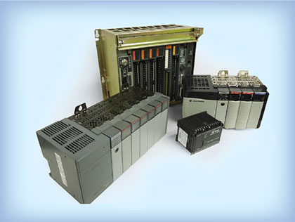
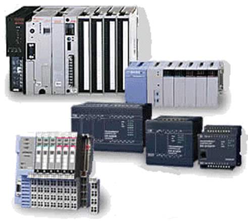
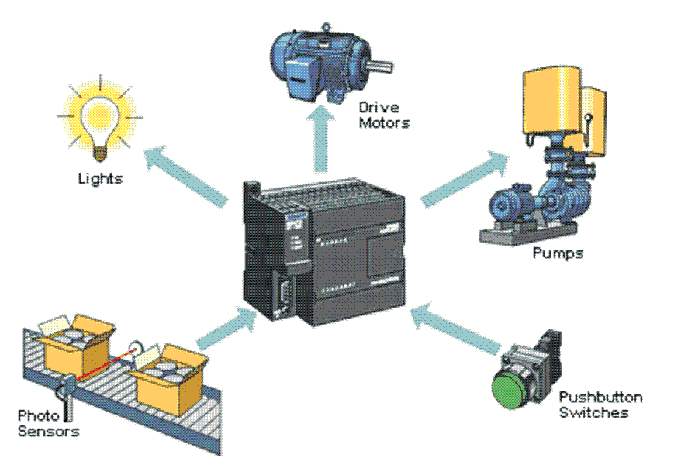
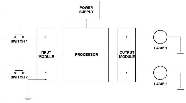

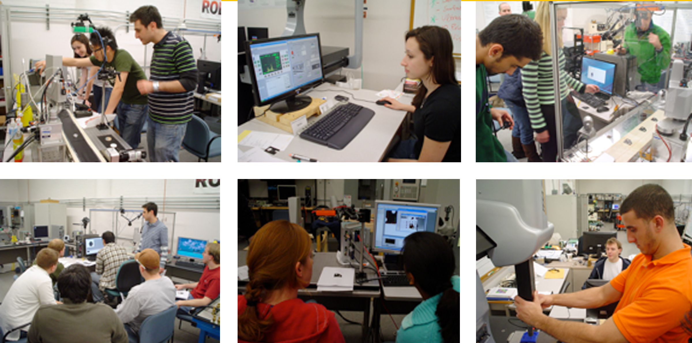
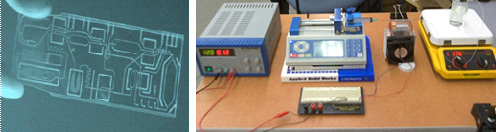
 The Lehmer sieve is an example of a digital non-electronic computer, specialized for finding primes and solving simple Diophantine equations. When digital electronic computers appeared, they displaced all other kinds of computers, including analog computers and mechanical computers .
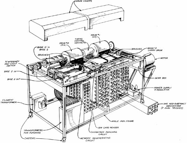
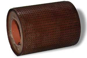 For storage device Atanasoff considered many possibilities, conducting numerous tests and experiments, in the end he chose to use for the memory a rotating electrostatic store—drum, based on capacitors. So called keyboard and counter drums (the nearby photo is of the only surviving part of the ABC—one of the two drums), are mounted on a common axle, were each eleven inches long and eight inches in diameter (the drums contained 1600 capacitors each). Each drum holds 30 numbers of 50 bits each. (Two of the columns are spares). Drums are operated in parallel. It is the first use of the idea we now call DRAM—use of capacitors to store 0s and 1s, refreshing their state periodically.
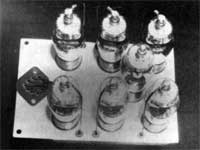 Atanasoff's arithmetic unit is based on vacuum tubes and consisted of thirty computing mechanisms together with several control mechanisms. Each of the computing mechanisms, which Atanasoff had expected to be electronic counters with some kind of carrying arrangement. That is, the thirty computing mechanisms consisted of thirty electronic add-subtract mechanisms (each contains 7 dual triodes) (see the nearby photo), thirty other primarily electronic mechanisms, and the thirty electrostatic bands of a carry-borrow drum.
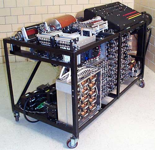

Thanks for this. I really like what you've posted here and wish you the best of luck with this blog and thanks for sharing. Desentupidora em Valinhos
BalasHapus