In the field of electronics science in the forefront of an electronic equipment there are two areas of component engineering block that is passive block and any active block called passive block is load block consists of:1. resistor or unit resistance ohms generate heat energy in the mode
trans2. inductor or unit winding henry generate magnetic energy in fashion
be linkage3. capacitor or condenser unit farad produce electrical energy in
linkage max modethe passive block in the control of electronics is the burden that generates the energy of conservation of the moment of inertia from one form of energy to anotherwhile the active block is the output perfection block to the load to generate a more perfect input on the passive block: the active block consists of:1. diode as refining the input into a power in
control2. transistors as driver tools and electronic switch in micro-nano order
seconds3. Integred circuit ie linear and digital pulses example 741 and 40474. microprocesor5. microcontroller6. computer7. wire memory flyer internet mode Tx and Rx reversible

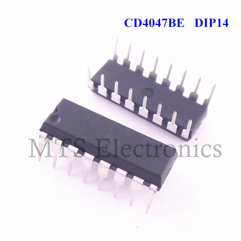
CD4047BC
Low Power Monostable/Astable Multivibrator
General Description
The CD4047B is capable of operating in either the
monostable or astable mode. It requires an external capacitor
(between pins 1 and 3) and an external resistor
(between pins 2 and 3) to determine the output pulse width
in the monostable mode, and the output frequency in the
astable mode.
Astable operation is enabled by a high level on the astable
input or low level on the astable input. The output frequency
(at 50% duty cycle) at Q and Q outputs is determined
by the timing components. A frequency twice that of
Q is available at the Oscillator Output; a 50% duty cycle is
not guaranteed.
Monostable operation is obtained when the device is triggered
by LOW-to-HIGH transition at + trigger input or
HIGH-to-LOW transition at - trigger input. The device can
be retriggered by applying a simultaneous LOW-to-HIGH
transition to both the + trigger and retrigger inputs.
A high level on Reset input resets the outputs Q to LOW, Q
to HIGH.
Features
n Wide supply voltage range: 3.0V to 15V
n High noise immunity: 0.45 VDD (typ.)
n Low power TTL compatibility: Fan out of 2 driving 74L
or 1 driving 74LS
SPECIAL FEATURES
n Low power consumption: special CMOS oscillator
configuration
n Monostable (one-shot) or astable (free-running)
operation
n True and complemented buffered outputs
n Only one external R and C required
MONOSTABLE MULTIVIBRATOR FEATURES
n Positive- or negative-edge trigger
n Output pulse width independent of trigger pulse duration
n Retriggerable option for pulse width expansion
n Long pulse widths possible using small RC components
by means of external counter provision
n Fast recovery time essentially independent of pulse
width
n Pulse-width accuracy maintained at duty cycles
approaching 100%
ASTABLE MULTIVIBRATOR FEATURES
n Free-running or gate able operating modes
n 50% duty cycle
n Oscillator output available
n Good astable frequency stability
typical= ±2% + 0.03%/°C @ 100 kHz
frequency= ±0.5% + 0.015%/°C @ 10 kHz
deviation (circuits trimmed to frequency VDD = 10V
±10%)
Applications
• Frequency discriminators
• Timing circuits
• Time-delay applications
• Envelope detection
• Frequency multiplication
• Frequency division

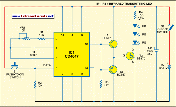
IC CD4047 basically it used for astable multivibrators for MOSFET's driving circuit (Gating Circuit).

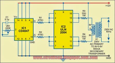
Simple Low-Power Inverter Circuit Diagram
CD4047BE / CD 4047BE, CMOS 4047 TIMERS /
ASTABLE MULTIVIBRATORS / MONOSTABLE MULTIVIBRATORS
LOW-POWER ICS (Much Superior to NE555/LM555)
The versatile 8-pin 555-series multivibrator ICs (LM 555 / NE 555) are probably the most popular ICs ever made. Unfortunately, not enough designers know the true power of the 14-pin CD 4047 timer / multivibrator IC! For a measely extra 3-pins on each side, here is the sizzling steak you get when you use the CMOS 4047 over the ground-round of the 555:
CMOS low power - on level with CMOS 555 ICs (ICM7555, LMC555, GLC555, LM7555). One big disadvantage with the LM555 is that it produces large crowbar currents in the output driver, resulting in supply current spikes of 300ma to 400ma when it switches, whereas the 4047 produces only 2ma - 3ma current spikes.
(2) Much higher bandwidth. 555 is limited to about 300 KHz. With the 4047, you get BW up to about 2 MHz (15+VDC supply).
(3) A + Trigger pin as well as a - Trigger pin. 555 has only a - Trigger pin.
(4) A Retrigger pin. Zip here for the 555.
(5) The normal Output pin plus the Complement Output pin. The 555 has only the normal Output pin. Complementary outputs much simplify switching, logic, push-pull and communications designs.
(6) Internal Oscillator Output pin. Zip here for the 555.
(7) Two Astable Inputs - one requiring positive voltage, the other requiring negative voltage to trigger Astable operation, else its Monostable. With the 555, to go from Astable to Monostable operation or vice-versa, you have to re-wire the timing circuitry by adding or removing a resistor. With the 4047, the timing circuitry conveniently stays the same; you just simply change the Astable or Not-Astable inputs.
For multivibrator versatility, you can't beat the 4047 CMOS. Because of these extra, often critical, advantages over the common 555, the 4047's multivibrator applications are virtually unlimited, and include: (1) Frequency multiplication, (2) Frequency division, (3) Envelope detection (e.g. amplitude modulation - AM demodulation), (4) Frequency discrimination, (5) Timing circuits / Time delay circuits. We use these standard ICs by the ton, but we purchased so many that we are selling some now. CD4047BE ICs shipped in anti-static tube.
Q . I Integrated circuit design
Integrated circuit design, or IC design, is a subset of electronics engineering, encompassing the particular logic and circuit design techniques required to design integrated circuits, or ICs. ICs consist of miniaturized electronic components built into an electrical network on a monolithic semiconductor substrate by photolithography.
IC design can be divided into the broad categories of digital and analog IC design. Digital IC design is to produce components such as microprocessors, FPGAs, memories (RAM, ROM, and flash) and digital ASICs. Digital design focuses on logical correctness, maximizing circuit density, and placing circuits so that clock and timing signals are routed efficiently. Analog IC design also has specializations in power IC design and RF IC design. Analog IC design is used in the design of op-amps, linear regulators, phase locked loops, oscillators and active filters. Analog design is more concerned with the physics of the semiconductor devices such as gain, matching, power dissipation, and resistance. Fidelity of analog signal amplification and filtering is usually critical and as a result, analog ICs use larger area active devices than digital designs and are usually less dense in circuitry.
Modern ICs are enormously complicated. An average desktop computer chip, as of 2015, has over 1 billion transistors. The rules for what can and cannot be manufactured are also extremely complex. Common IC processes of 2015 have more than 500 rules. Furthermore, since the manufacturing process itself is not completely predictable, designers must account for its statistical nature. The complexity of modern IC design, as well as market pressure to produce designs rapidly, has led to the extensive use of automated design tools in the IC design process. In short, the design of an IC using EDA software is the design, test, and verification of the instructions that the IC is to carry out.

Layout view of a simple CMOS Operational Amplifier (inputs are to the left and the compensation capacitor is to the right). The metal layer is coloured blue, green and brown are N- and P-doped Si, the polysilicon is red and vias are crosses
Integrated circuit design involves the creation of electronic components, such as transistors, resistors, capacitors and the metallic interconnect of these components onto a piece of semiconductor, typically silicon. A method to isolate the individual components formed in the substrate is necessary since the substrate silicon is conductive and often forms an active region of the individual components. The two common methods are p-n junction isolation and dielectric isolation. Attention must be given to power dissipation of transistors and interconnect resistances and current density of the interconnect, contacts and vias since ICs contain very tiny devices compared to discrete components, where such concerns are less of an issue. Electromigration in metallic interconnect and ESD damage to the tiny components are also of concern. Finally, the physical layout of certain circuit subblocks is typically critical, in order to achieve the desired speed of operation, to segregate noisy portions of an IC from quiet portions, to balance the effects of heat generation across the IC, or to facilitate the placement of connections to circuitry outside the IC.
Design steps
A typical IC design cycle involves several steps:
- Feasibility study and die size estimate
- Function analysis
- System Level Design
- Analogue Design, Simulation & Layout
- Digital Design, Simulation & Synthesis
- System Simulation & Verification
- Design For Test and Automatic test pattern generation
- Design for manufacturability (IC)
- Tape-in
- Mask data preparation
- Tape-out
- Wafer fabrication
- Die test
- Packaging
- Post silicon validation and integration
- Device characterization
- Tweak (if necessary)
- Datasheet generation (of usually a Portable Document Format (PDF) file)
- Ramp up
- Production
- Yield Analysis / Warranty Analysis Reliability (semiconductor)
- Failure analysis on any returns
- Plan for next generation chip using production information if possible
- Electronic system-level design: This step creates the user functional specification. The user may use a variety of languages and tools to create this description. Examples include a C/C++ model, SystemC, SystemVerilog Transaction Level Models, Simulink and MATLAB.
- RTL design: This step converts the user specification (what the user wants the chip to do) into a register transfer level (RTL) description. The RTL describes the exact behavior of the digital circuits on the chip, as well as the interconnections to inputs and outputs.
- Physical design: This step takes the RTL, and a library of available logic gates, and creates a chip design. This involves figuring out which gates to use, defining places for them, and wiring them together.
Design process
Microarchitecture and system-level design
The initial chip design process begins with system-level design and microarchitecture planning. Within IC design companies, management and often analytics will draft a proposal for a design team to start the design of a new chip to fit into an industry segment. Upper-level designers will meet at this stage to decide how the chip will operate functionally. This step is where an IC's functionality and design are decided. IC designers will map out the functional requirements, verification testbenches, and testing methodologies for the whole project, and will then turn the preliminary design into a system-level specification that can be simulated with simple models using languages like C++ and MATLAB and emulation tools. For pure and new designs, the system design stage is where an Instruction set and operation is planned out, and in most chips existing instruction sets are modified for newer functionality. Design at this stage is often statements such as encodes in the MP3 format or implements IEEE floating-point arithmetic. At later stages in the design process, each of these innocent looking statements expands to hundreds of pages of textual documentation.RTL design
Upon agreement of a system design, RTL designers then implement the functional models in a hardware description language like Verilog, SystemVerilog, or VHDL. Using digital design components like adders, shifters, and state machines as well as computer architecture concepts like pipelining, superscalar execution, and branch prediction, RTL designers will break a functional description into hardware models of components on the chip working together. Each of the simple statements described in the system design can easily turn into thousands of lines of RTL code, which is why it is extremely difficult to verify that the RTL will do the right thing in all the possible cases that the user may throw at it.To reduce the number of functionality bugs, a separate hardware verification group will take the RTL and design testbenches and systems to check that the RTL actually is performing the same steps under many different conditions, classified as the domain of functional verification. Many techniques are used, none of them perfect but all of them useful – extensive logic simulation, formal methods, hardware emulation, lint-like code checking, code coverage, and so on.
A tiny error here can make the whole chip useless, or worse. The famous Pentium FDIV bug caused the results of a division to be wrong by at most 61 parts per million, in cases that occurred very infrequently. No one even noticed it until the chip had been in production for months. Yet Intel was forced to offer to replace, for free, every chip sold until they could fix the bug, at a cost of $475 million (US).
Physical design
RTL is only a behavioral model of the actual functionality of what the chip is supposed to operate under. It has no link to a physical aspect of how the chip would operate in real life at the materials, physics, and electrical engineering side. For this reason, the next step in the IC design process, physical design stage, is to map the RTL into actual geometric representations of all electronics devices, such as capacitors, resistors, logic gates, and transistors that will go on the chip.
The main steps of physical design are listed below. In practice there is not a straightforward progression - considerable iteration is required to ensure all objectives are met simultaneously. This is a difficult problem in its own right, called design closure.
- Logic synthesis: The RTL is mapped into a gate-level netlist in the target technology of the chip.
- Floorplanning: The RTL of the chip is assigned to gross regions of the chip, input/output (I/O) pins are assigned and large objects (arrays, cores, etc.) are placed.
- Placement: The gates in the netlist are assigned to nonoverlapping locations on the die area.
- Logic/placement refinement: Iterative logical and placement transformations to close performance and power constraints.
- Clock insertion: Clock signal wiring is (commonly, clock trees) introduced into the design.
- Routing: The wires that connect the gates in the netlist are added.
- Postwiring optimization: Performance (timing closure), noise (signal integrity), and yield (Design for manufacturability) violations are removed.
- Design for manufacturability: The design is modified, where possible, to make it as easy and efficient as possible to produce. This is achieved by adding extra vias or adding dummy metal/diffusion/poly layers wherever possible while complying to the design rules set by the foundry.
- Final checking: Since errors are expensive, time consuming and hard to spot, extensive error checking is the rule, making sure the mapping to logic was done correctly, and checking that the manufacturing rules were followed faithfully.
- Tapeout and mask generation: the design data is turned into photomasks in mask data preparation.
Analog design
Before the advent of the microprocessor and software based design tools, analog ICs were designed using hand calculations and process kit parts. These ICs were low complexity circuits, for example, op-amps, usually involving no more than ten transistors and few connections. An iterative trial-and-error process and "overengineering" of device size was often necessary to achieve a manufacturable IC. Reuse of proven designs allowed progressively more complicated ICs to be built upon prior knowledge. When inexpensive computer processing became available in the 1970s, computer programs were written to simulate circuit designs with greater accuracy than practical by hand calculation. The first circuit simulator for analog ICs was called SPICE (Simulation Program with Integrated Circuits Emphasis). Computerized circuit simulation tools enable greater IC design complexity than hand calculations can achieve, making the design of analog ASICs practical. The computerized circuit simulators also enable mistakes to be found early in the design cycle before a physical device is fabricated. Additionally, a computerized circuit simulator can implement more sophisticated device models and circuit analysis too tedious for hand calculations, permitting Monte Carlo analysis and process sensitivity analysis to be practical. The effects of parameters such as temperature variation, doping concentration variation and statistical process variations can be simulated easily to determine if an IC design is manufacturable. Overall, computerized circuit simulation enables a higher degree of confidence that the circuit will work as expected upon manufacture.Coping with variability
A challenge most critical to analog IC design involves the variability of the individual devices built on the semiconductor chip. Unlike board-level circuit design which permits the designer to select devices that have each been tested and binned according to value, the device values on an IC can vary widely which are uncontrollable by the designer. For example, some IC resistors can vary ±20% and β of an integrated BJT can vary from 20 to 100. In the latest CMOS processes, β of vertical PNP transistors can even go below 1. To add to the design challenge, device properties often vary between each processed semiconductor wafer. Device properties can even vary significantly across each individual IC due to doping gradients. The underlying cause of this variability is that many semiconductor devices are highly sensitive to uncontrollable random variances in the process. Slight changes to the amount of diffusion time, uneven doping levels, etc. can have large effects on device properties.Some design techniques used to reduce the effects of the device variation are:
- Using the ratios of resistors, which do match closely, rather than absolute resistor value.
- Using devices with matched geometrical shapes so they have matched variations.
- Making devices large so that statistical variations becomes an insignificant fraction of the overall device property.
- Segmenting large devices, such as resistors, into parts and interweaving them to cancel variations.
- Using common centroid device layout to cancel variations in devices which must match closely (such as the transistor differential pair of an op amp).
Vendors
The three largest companies selling electronic design automation tools are Synopsys, Cadence, and Mentor GraphicsQ . II Electronic design automation
Electronic design automation (EDA), also referred to as electronic computer-aided design (ECAD), is a category of software tools for designing electronic systems such as integrated circuits and printed circuit boards. The tools work together in a design flow that chip designers use to design and analyze entire semiconductor chips. Since a modern semiconductor chip can have billions of components, EDA tools are essential for their design.
EDA specifically with respect to integrated circuits.
Before EDA, integrated circuits were designed by hand, and manually laid out. Some advanced shops used geometric software to generate the tapes for the Gerber photoplotter, but even those copied digital recordings of mechanically drawn components. The process was fundamentally graphic, with the translation from electronics to graphics done manually. The best known company from this era was Calma, whose GDSII format survives.
By the mid-1970s, developers started to automate the design along with the drafting. The first placement and routing (Place and route) tools were developed. The proceedings of the Design Automation Conference cover much of this era.
The next era began about the time of the publication of "Introduction to VLSI Systems" by Carver Mead and Lynn Conway in 1980. This ground breaking text advocated chip design with programming languages that compiled to silicon. The immediate result was a considerable increase in the complexity of the chips that could be designed, with improved access to design verification tools that used logic simulation. Often the chips were easier to lay out and more likely to function correctly, since their designs could be simulated more thoroughly prior to construction. Although the languages and tools have evolved, this general approach of specifying the desired behavior in a textual programming language and letting the tools derive the detailed physical design remains the basis of digital IC design today.
The earliest EDA tools were produced academically. One of the most famous was the "Berkeley VLSI Tools Tarball", a set of UNIX utilities used to design early VLSI systems. Still widely used are the Espresso heuristic logic minimizer and Magic.
Another crucial development was the formation of MOSIS, a consortium of universities and fabricators that developed an inexpensive way to train student chip designers by producing real integrated circuits. The basic concept was to use reliable, low-cost, relatively low-technology IC processes, and pack a large number of projects per wafer, with just a few copies of each projects' chips. Cooperating fabricators either donated the processed wafers, or sold them at cost, seeing the program as helpful to their own long-term growth.
Birth of commercial EDA
1981 marks the beginning of EDA as an industry. For many years, the larger electronic companies, such as Hewlett Packard, Tektronix, and Intel, had pursued EDA internally. In 1981, managers and developers spun out of these companies to concentrate on EDA as a business. Daisy Systems, Mentor Graphics, and Valid Logic Systems were all founded around this time, and collectively referred to as DMV. Within a few years there were many companies specializing in EDA, each with a slightly different emphasis. The first trade show for EDA was held at the Design Automation Conference in 1984.In 1981, the U.S. Department of Defense began funding of VHDL as a hardware description language. In 1986, Verilog, another popular high-level design language, was first introduced as a hardware description language by Gateway Design Automation. Simulators quickly followed these introductions, permitting direct simulation of chip designs: executable specifications. In a few more years, back-ends were developed to perform logic synthesis.

Current status
Current digital flows are extremely modular The front ends produce standardized design descriptions that compile into invocations of "cells,", without regard to the cell technology. Cells implement logic or other electronic functions using a particular integrated circuit technology. Fabricators generally provide libraries of components for their production processes, with simulation models that fit standard simulation tools. Analog EDA tools are far less modular, since many more functions are required, they interact more strongly, and the components are (in general) less ideal.EDA for electronics has rapidly increased in importance with the continuous scaling of semiconductor technology.[2] Some users are foundry operators, who operate the semiconductor fabrication facilities, or "fabs", and design-service companies who use EDA software to evaluate an incoming design for manufacturing readiness. EDA tools are also used for programming design functionality into FPGAs.
- High-level synthesis (or behavioural synthesis, algorithmic synthesis) – high-level design description (e.g. in C/C++) is converted into RTL.
- Logic synthesis – translation of RTL design description (e.g. written in Verilog or VHDL) into a discrete netlist of logic gates.
- Schematic capture – For standard cell digital, analog, RF-like Capture CIS in Orcad by Cadence and ISIS in Proteus
- Layout – usually schematic-driven layout, like Layout in Orcad by Cadence, ARES in Proteus
Simulation
- Transistor simulation – low-level transistor-simulation of a schematic/layout's behavior, accurate at device-level.
- Logic simulation – digital-simulation of an RTL or gate-netlist's digital (boolean 0/1) behavior, accurate at boolean-level.
- Behavioral Simulation – high-level simulation of a design's architectural operation, accurate at cycle-level or interface-level.
- Hardware emulation – Use of special purpose hardware to emulate the logic of a proposed design. Can sometimes be plugged into a system in place of a yet-to-be-built chip; this is called in-circuit emulation.
- Technology CAD simulate and analyze the underlying process technology. Electrical properties of devices are derived directly from device physics.
- Electromagnetic field solvers, or just field solvers, solve Maxwell's equations directly for cases of interest in IC and PCB design. They are known for being slower but more accurate than the layout extraction above.[where?]

Analysis and verification
- Functional verification
- Clock Domain Crossing Verification (CDC check): Similar to linting, but these checks/tools specialize in detecting and reporting potential issues like data loss, meta-stability due to use of multiple clock domains in the design.
- Formal verification, also model checking: Attempts to prove, by mathematical methods, that the system has certain desired properties, and that certain undesired effects (such as deadlock) cannot occur.
- Equivalence checking: algorithmic comparison between a chip's RTL-description and synthesized gate-netlist, to ensure functional equivalence at the logical level.
- Static timing analysis: Analysis of the timing of a circuit in an input-independent manner, hence finding a worst case over all possible inputs.
- Physical verification, PV: checking if a design is physically manufacturable, and that the resulting chips will not have any function-preventing physical defects, and will meet original specifications.
Manufacturing preparation
- Mask data preparation, MDP: generation of actual lithography photomask used to physically manufacture the chip.
- Resolution enhancement techniques, RET – methods of increasing of quality of final photomask.
- Optical proximity correction, OPC – up-front compensation for diffraction and interference effects occurring later when chip is manufactured using this mask.
- Mask generation – generation of flat mask image from hierarchical design.
- Automatic test pattern generation, ATPG – generates pattern-data to systematically exercise as many logic-gates, and other components, as possible.
- Built-in self-test, or BIST – installs self-contained test-controllers to automatically test a logic (or memory) structure in the design
Functional Safety
- Functional Safety Analysis, Systematic computation of failure in time (FIT) rates and diagnostic coverage metrics for designs in order to meet the compliance requirements for the desired safety integrity levels.
- Functional Safety Synthesis, Add reliability enhancements to structured elements (Modules, RAMs, ROMs, Register Files, FIFOs) to improves fault detection / fault tolerance. These includes (not limited to), Addition of error detection and / or correction codes (Hamming), Redundant logic for fault detection and fault tolerance (duplicate / triplicate) and Protocol checks (Interface parity, address alignment, beat count)
- Functional Safety Verification,Running of a fault campaign, including insertion of faults into the design and verification that the safety mechanism reacts in an appropriate manner for the faults that are deemed covered.

Acquisitions
Many of the EDA companies acquire small companies with software or other technology that can be adapted to their core business. Most of the market leaders are amalgamations of many smaller companies.This trend is helped by the tendency of software companies to design tools as accessories that fit naturally into a larger vendor's suite of programs on digital circuitry, many new tools incorporate analog design, and mixed systems. This is happening because there is now a trend to place entire electronic systems on a single chip.Q . III Signoff (electronic design automation)
In the automated design of integrated circuits, signoff (also written as sign-off) checks is the collective name given to a series of verification steps that the design must pass before it can be taped out. This implies an iterative process involving incremental fixes across the board using one or more check types, and then retesting the design. There are two types of sign-off's: front-end sign-off and back-end sign-off. After back-end sign-off the chip goes to fabrication. After listing out all the features in the specification, the verification engineer will write coverage for those features to identify bugs, and send back the RTL design to the designer. Bugs, or defects, can include issues like missing features (comparing the layout to the specification), errors in design (typo and functional errors), etc. When the coverage reaches a maximum% then the verification team will sign it off. By using a methodology like UVM, OVM, or VMM, the verification team develops a reusable environment. Nowadays, UVM is more popular than others.
While vendors often embellish the ease of end-to-end (typically RTL to GDS for ASICs, and RTL to timing closure for FPGAs) execution through their respective tool suite, most semiconductor design companies use a combination of tools from various vendors (often called "best of breed" tools) in order to minimize correlation errors pre- and post-silicon. Since independent tool evaluation is expensive (single licenses for design tools from major vendors like Synopsys and Cadence may cost tens or hundreds of thousands of dollars) and a risky proposition (if the failed evaluation is done on a production design, resulting in a time to market delay), it is feasible only for the largest design companies (like Intel, IBM, Freescale, and TI). As a value add, several semiconductor foundries now provide pre-evaluated reference/recommended methodologies (sometimes referred to as "RM" flows) which includes a list of recommended tools, versions, and scripts to move data from one tool to another and automate the entire process
Check types
Signoff checks have become more complex as VLSI designs approach 22nm and below process nodes, because of the increased impact of previously ignored (or more crudely approximated) second-order effects. There are several categories of signoff checks.- DRC – Also sometimes known as geometric verification, this involves verifying if the design can be reliably manufactured given current photolithography limitations. In advanced process nodes, DFM rules are upgraded from optional (for better yield) to required.
- LVS – Also known as schematic verification, this is used to verify that the placement and routing of the standard cells in the design has not altered the functionality of the constructed circuit.
- Formal verification – Here, the logical functionality of the post-layout netlist (including any layout-driven optimization) is verified against the pre-layout, post-synthesis netlist.
- Voltage drop analysis – Also known as IR-drop analysis, this check verifies if the power grid is strong enough to ensure that the voltage representing the binary high value never dips lower than a set margin (below which the circuit will not function correctly or reliably) due to the combined switching of millions of transistors.
- Signal integrity analysis – Here, noise due to crosstalk and other issues is analyzed, and its effect on circuit functionality is checked to ensure that capacitive glitches are not large enough to cross the threshold voltage of gates along the data path.
- Static timing analysis (STA) – Slowly being superseded by statistical static timing analysis (SSTA), STA is used to verify if all the logic data paths in the design can work at the intended clock frequency, especially under the effects of on-chip variation. STA is run as a replacement for SPICE, because SPICE simulation's runtime makes it infeasible for full-chip analysis modern designs.
- Electromigration lifetime checks – To ensure a minimum lifetime of operation at the intended clock frequency without the circuit succumbing to electromigration.
Tools
A small subset of tools are classified as "golden" or signoff-quality. Categorizing a tool as signoff-quality without vendor-bias is a matter of trial and error, since the accuracy of the tool can only be determined after the design has been fabricated. So, one of the metrics that is in use (and often touted by the tool manufacturer/vendor) is the number of successful tapeouts enabled by the tool in question. It has been argued that this metric is insufficient, ill-defined, and irrelevant for certain tools, especially tools that play only a part in the full flow.While vendors often embellish the ease of end-to-end (typically RTL to GDS for ASICs, and RTL to timing closure for FPGAs) execution through their respective tool suite, most semiconductor design companies use a combination of tools from various vendors (often called "best of breed" tools) in order to minimize correlation errors pre- and post-silicon. Since independent tool evaluation is expensive (single licenses for design tools from major vendors like Synopsys and Cadence may cost tens or hundreds of thousands of dollars) and a risky proposition (if the failed evaluation is done on a production design, resulting in a time to market delay), it is feasible only for the largest design companies (like Intel, IBM, Freescale, and TI). As a value add, several semiconductor foundries now provide pre-evaluated reference/recommended methodologies (sometimes referred to as "RM" flows) which includes a list of recommended tools, versions, and scripts to move data from one tool to another and automate the entire process
Q . IIIII Integrated circuit development
The integrated circuit (IC) development process starts with defining product requirements, progresses through architectural definition, implementation, bringup and finally productization. The various phases of the integrated circuit development process are described below. Although the phases are presented here in a straightforward fashion, in reality there is iteration and these steps may occur multiple times.
Before an architecture can be defined some high level product goals must be defined. The requirements are usually generated by a cross functional team that addresses market opportunity, customer needs, feasibility and much more. This phase should result in a product requirements document.
Architecture
The architecture defines the fundamental structure, goals and principles of the product. It defines high level concepts and the intrinsic value proposition of the product. Architecture teams take into account many variables and interface with many groups. People creating the architecture generally have a significant amount of experience dealing with systems in the area for which the architecture is being created. The work product of the architecture phase is an architectural specification.Micro-architecture
The micro-architecture is a step closer to the hardware. It implements the architecture and defines specific mechanisms and structures for achieving that implementation. The result of the micro-architecture phase is a micro-architecture specification which describes the methods used to implement the architecture.Implementation
In the implementation phase the design itself is created using the micro-architectural specification as the starting point. This involves low level definition and partitioning, writing code, entering schematics and verification. This phase ends with a design reaching tapeout.Bring up
After a design is created, taped-out and manufactured, actual hardware, 'first silicon', is received which is taken into the lab where it goes through bringup. Bringup is the process of powering, testing and characterizing the design in the lab. Numerous tests are performed starting from very simple tests such as ensuring that the device will power on to much more complicated tests which try to stress the part in various ways. The result of the bringup phase is documentation of characterization data (how well the part performs to spec) and errata (unexpected behavior).Productization
Productization is the task of taking a design from engineering into mass production manufacturing. Although a design may have successfully met the specifications of the product in the lab during the bringup phase there are many challenges that face product engineers when trying to mass-produce those designs. The IC must be ramped up to production volumes with an acceptable yield. The goal of the productization phase is to reach mass production volumes at an acceptable cost.Sustaining
Once a design is mature and has reached mass production it must be sustained. The process must be continually monitored and problems dealt with quickly to avoid a significant impact on production volumes. The goal of sustaining is to maintain production volumes and continually reduce costs until the product reaches end of life .Q . IIIIII Microprocessor
A microprocessor is a computer processor which incorporates the functions of a computer's central processing unit (CPU) on a single integrated circuit (IC), or at most a few integrated circuits.[2] The microprocessor is a multipurpose, clock driven, register based, digital-integrated circuit which accepts binary data as input, processes it according to instructions stored in its memory, and provides results as output. Microprocessors contain both combinational logic and sequential digital logic. Microprocessors operate on numbers and symbols represented in the binary numeral system.
The integration of a whole CPU onto a single chip or on a few chips greatly reduced the cost of processing power, increasing efficiency. Integrated circuit processors are produced in large numbers by highly automated processes resulting in a low per unit cost. Single-chip processors increase reliability as there are many fewer electrical connections to fail. As microprocessor designs get better, the cost of manufacturing a chip (with smaller components built on a semiconductor chip the same size) generally stays the same.
Before microprocessors, small computers had been built using racks of circuit boards with many medium- and small-scale integrated circuits. Microprocessors combined this into one or a few large-scale ICs. Continued increases in microprocessor capacity have since rendered other forms of computers almost completely obsolete (see history of computing hardware), with one or more microprocessors used in everything from the smallest embedded systems and handheld devices to the largest mainframes and supercomputers


Structure

A block diagram of the architecture of the Z80 microprocessor, showing the arithmetic and logic section, register file, control logic section, and buffers to external address and data lines
A minimal hypothetical microprocessor might only include an arithmetic logic unit (ALU) and a control logic section. The ALU performs operations such as addition, subtraction, and operations such as AND or OR. Each operation of the ALU sets one or more flags in a status register, which indicate the results of the last operation (zero value, negative number, overflow, or others). The control logic retrieves instruction codes from memory and initiates the sequence of operations required for the ALU to carry out the instruction. A single operation code might affect many individual data paths, registers, and other elements of the processor.
As integrated circuit technology advanced, it was feasible to manufacture more and more complex processors on a single chip. The size of data objects became larger; allowing more transistors on a chip allowed word sizes to increase from 4- and 8-bit words up to today's 64-bit words. Additional features were added to the processor architecture; more on-chip registers sped up programs, and complex instructions could be used to make more compact programs. Floating-point arithmetic, for example, was often not available on 8-bit microprocessors, but had to be carried out in software. Integration of the floating point unit first as a separate integrated circuit and then as part of the same microprocessor chip, sped up floating point calculations.
Occasionally, physical limitations of integrated circuits made such practices as a bit slice approach necessary. Instead of processing all of a long word on one integrated circuit, multiple circuits in parallel processed subsets of each data word. While this required extra logic to handle, for example, carry and overflow within each slice, the result was a system that could handle, for example, 32-bit words using integrated circuits with a capacity for only four bits each.
With the ability to put large numbers of transistors on one chip, it becomes feasible to integrate memory on the same die as the processor. This CPU cache has the advantage of faster access than off-chip memory, and increases the processing speed of the system for many applications. Processor clock frequency has increased more rapidly than external memory speed, except in the recent past,[when?] so cache memory is necessary if the processor is not delayed by slower external memory.
Special-purpose designs
A microprocessor is a general purpose system. Several specialized processing devices have followed from the technology:- A digital signal processor (DSP) is specialized for signal processing.
- Graphics processing units (GPUs) are processors designed primarily for realtime rendering of 3D images. They may be fixed function (as was more common in the 1990s), or support programmable shaders. With the continuing rise of GPGPU, GPUs are evolving into increasingly general purpose stream processors (running compute shaders), whilst retaining hardware assist for rasterizing, but still differ from CPUs in that they are optimized for throughput over latency, and are not suitable for running application or OS code.
- Other specialized units exist for video processing and machine vision.
- Microcontrollers integrate a microprocessor with peripheral devices in embedded systems. These tend to have different tradeoffs compared to CPUs.
Nevertheless, trade-offs apply: running 32-bit arithmetic on an 8-bit chip could end up using more power, as the chip must execute software with multiple instructions. Modern microprocessors go into low power states when possible, and an 8-bit chip running 32-bit calculations would be active for more cycles. This creates a delicate balance between software, hardware and use patterns, plus costs
When manufactured on a similar process, 8-bit microprocessors use less power when operating and less power when sleeping than 32-bit microprocessors.
However, a 32-bit microprocessor may use less average power than an 8-bit microprocessor when the application requires certain operations such as floating-point math that take many more clock cycles on an 8-bit microprocessor than a 32-bit microprocessor so the 8-bit microprocessor spends more time in high-power operating mode
Embedded applications
Thousands of items that were traditionally not computer-related include microprocessors. These include large and small household appliances, cars (and their accessory equipment units), car keys, tools and test instruments, toys, light switches/dimmers and electrical circuit breakers, smoke alarms, battery packs, and hi-fi audio/visual components (from DVD players to phonograph turntables). Such products as cellular telephones, DVD video system and HDTV broadcast systems fundamentally require consumer devices with powerful, low-cost, microprocessors. Increasingly stringent pollution control standards effectively require automobile manufacturers to use microprocessor engine management systems, to allow optimal control of emissions over widely varying operating conditions of an automobile. Non-programmable controls would require complex, bulky, or costly implementation to achieve the results possible with a microprocessor.A microprocessor control program (embedded software) can be easily tailored to different needs of a product line, allowing upgrades in performance with minimal redesign of the product. Different features can be implemented in different models of a product line at negligible production cost.
Microprocessor control of a system can provide control strategies that would be impractical to implement using electromechanical controls or purpose-built electronic controls. For example, an engine control system in an automobile can adjust ignition timing based on engine speed, load on the engine, ambient temperature, and any observed tendency for knocking—allowing an automobile to operate on a range of fuel grades
The advent of low-cost computers on integrated circuits has transformed modern society. General-purpose microprocessors in personal computers are used for computation, text editing, multimedia display, and communication over the Internet. Many more microprocessors are part of embedded systems, providing digital control over myriad objects from appliances to automobiles to cellular phones and industrial process control.
The first use of the term "microprocessor" is attributed to Viatron Computer Systems describing the custom integrated circuit used in their System 21 small computer system announced in 1968.
By the late-1960s, designers were striving to integrate the central processing unit (CPU) functions of a computer onto a handful of MOS LSI chips, called microprocessor unit (MPU) chipsets. Building on an earlier Busicom design from 1969, Intel introduced the first commercial microprocessor, the 4-bit Intel 4004, in 1971, followed by its 8-bit microprocessor 8008 in 1972. Building on 8-bit arithmetic logic units (3800/3804) he designed earlier at Fairchild, in 1969, Lee Boysel created the Four-Phase Systems Inc. AL-1 an 8-bit CPU slice that was expandable to 32-bits. In 1970, Steve Geller and Ray Holt of Garrett AiResearch designed the MP944 chipset to implement the F-14A Central Air Data Computer on six metal-gate chips fabricated by AMI.
During the 1960s, computer processors were constructed out of small and medium-scale ICs—each containing from tens of transistors to a few hundred. These were placed and soldered onto printed circuit boards, and often multiple boards were interconnected in a chassis. A large number of discrete logic gates uses more electrical power—and therefore produces more heat—than a more integrated design with fewer ICs. The distance that signals have to travel between ICs on the boards limits a computer's operating system speed.
In the NASA Apollo space missions to the moon in the 1960s and 1970s, all onboard computations for primary guidance, navigation, and control were provided by a small custom processor called "The Apollo Guidance Computer". It used wire wrap circuit boards whose only logic elements were three-input NOR gates.[11]
The first microprocessors emerged in the early 1970s, and were used for electronic calculators, using binary-coded decimal (BCD) arithmetic on 4-bit words. Other embedded uses of 4-bit and 8-bit microprocessors, such as terminals, printers, various kinds of automation etc., followed soon after. Affordable 8-bit microprocessors with 16-bit addressing also led to the first general-purpose microcomputers from the mid-1970s on.
Since the early 1970s, the increase in capacity of microprocessors has followed Moore's law; this originally suggested that the number of components that can be fitted onto a chip doubles every year. With present technology, it is actually every two years,[12] and as such Moore later changed the period to two years.[13]
First projects
Three projects delivered a microprocessor at about the same time: Intel's 4004 (1971 November, based on an earlier 1969 Busicom design), Garrett AiResearch's Central Air Data Computer (CADC), and Texas Instruments (TI) TMS 1000 (1971 September). Arguably, Four-Phase Systems AL1 microprocessor was also delivered in 1969.Intel 4004 (1969-1971)
.jpg)
The 4004 with cover removed (left) and as actually used (right)
The project that produced the 4004 originated in 1969, when Busicom, a Japanese calculator manufacturer, asked Intel to build a chipset for high-performance desktop calculators. Busicom's original design called for a programmable chip set consisting of seven different chips. Three of the chips were to make a special-purpose CPU with its program stored in ROM and its data stored in shift register read-write memory. Ted Hoff, the Intel engineer assigned to evaluate the project, believed the Busicom design could be simplified by using dynamic RAM storage for data, rather than shift register memory, and a more traditional general-purpose CPU architecture. Hoff came up with a four-chip architectural proposal: a ROM chip for storing the programs, a dynamic RAM chip for storing data, a simple I/O device and a 4-bit central processing unit (CPU). Although not a chip designer, he felt the CPU could be integrated into a single chip, but as he lacked the technical know-how the idea remained just a wish for the time being.

Intel 4004, the first commercial microprocessor

CADC.
In 1968, Garrett AiResearch (who employed designers Ray Holt and Steve Geller) was invited to produce a digital computer to compete with electromechanical systems then under development for the main flight control computer in the US Navy's new F-14 Tomcat fighter. The design was complete by 1970, and used a MOS-based chipset as the core CPU. The design was significantly (approximately 20 times) smaller and much more reliable than the mechanical systems it competed against, and was used in all of the early Tomcat models. This system contained "a 20-bit, pipelined, parallel multi-microprocessor". The Navy refused to allow publication of the design until 1997. For this reason the CADC, and the MP944 chipset it used, are fairly unknown.[19]Ray Holt graduated from California Polytechnic University in 1968, and began his computer design career with the CADC. From its inception, it was shrouded in secrecy until 1998 when at Holt's request, the US Navy allowed the documents into the public domain. Since then people[who?] have debated whether this was the first microprocessor. Holt has stated that no one has compared this microprocessor with those that came later.[20] According to Parab et al. (2007),
The scientific papers and literature published around 1971 reveal that the MP944 digital processor used for the F-14 Tomcat aircraft of the US Navy qualifies as the first microprocessor. Although interesting, it was not a single-chip processor, as was not the Intel 4004 – they both were more like a set of parallel building blocks you could use to make a general-purpose form. It contains a CPU, RAM, ROM, and two other support chips like the Intel 4004. It was made from the same P-channel technology, operated at military specifications and had larger chips – an excellent computer engineering design by any standards. Its design indicates a major advance over Intel, and two year earlier. It actually worked and was flying in the F-14 when the Intel 4004 was announced. It indicates that today's industry theme of converging DSP-microcontroller architectures was started in 1971.[21]This convergence of DSP and microcontroller architectures is known as a digital signal controller.
Four-Phase Systems AL1 (1969)

Pico/General Instrument

Pico was a spinout by five GI design engineers whose vision was to create single chip calculator ICs. They had significant previous design experience on multiple calculator chipsets with both GI and Marconi-Elliott.[29] The key team members had originally been tasked by Elliott Automation to create an 8-bit computer in MOS and had helped establish a MOS Research Laboratory in Glenrothes, Scotland in 1967.
Calculators were becoming the largest single market for semiconductors so Pico and GI went on to have significant success in this burgeoning market. GI continued to innovate in microprocessors and microcontrollers with products including the CP1600, IOB1680 and PIC1650. In 1987, the GI Microelectronics business was spun out into the Microchip PIC microcontroller business.
Gilbert Hyatt
Gilbert Hyatt was awarded a patent claiming an invention pre-dating both TI and Intel, describing a "microcontroller". The patent was later invalidated, but not before substantial royalties were paid outTMS 1000
The Smithsonian Institution says TI engineers Gary Boone and Michael Cochran succeeded in creating the first microcontroller (also called a microcomputer) and the first single-chip CPU in 1971. The result of their work was the TMS 1000, which went on the market in 1974.[34] TI stressed the 4-bit TMS 1000 for use in pre-programmed embedded applications, introducing a version called the TMS1802NC on September 17, 1971 that implemented a calculator on a chip.TI filed for a patent on the microprocessor. Gary Boone was awarded U.S. Patent 3,757,306 for the single-chip microprocessor architecture on September 4, 1973. In 1971, and again in 1976, Intel and TI entered into broad patent cross-licensing agreements, with Intel paying royalties to TI for the microprocessor patent. A history of these events is contained in court documentation from a legal dispute between Cyrix and Intel, with TI as inventor and owner of the microprocessor patent.
A computer-on-a-chip combines the microprocessor core (CPU), memory, and I/O (input/output) lines onto one chip. The computer-on-a-chip patent, called the "microcomputer patent" at the time, U.S. Patent 4,074,351, was awarded to Gary Boone and Michael J. Cochran of TI. Aside from this patent, the standard meaning of microcomputer is a computer using one or more microprocessors as its CPU(s), while the concept defined in the patent is more akin to a microcontroller.
The Intel 4004 was followed in 1972 by the Intel 8008, the world's first 8-bit microprocessor. The 8008 was not, however, an extension of the 4004 design, but instead the culmination of a separate design project at Intel, arising from a contract with Computer Terminals Corporation, of San Antonio TX, for a chip for a terminal they were designing,[35] the Datapoint 2200—fundamental aspects of the design came not from Intel but from CTC. In 1968, CTC's Vic Poor and Harry Pyle developed the original design for the instruction set and operation of the processor. In 1969, CTC contracted two companies, Intel and Texas Instruments, to make a single-chip implementation, known as the CTC 1201.[36] In late 1970 or early 1971, TI dropped out being unable to make a reliable part. In 1970, with Intel yet to deliver the part, CTC opted to use their own implementation in the Datapoint 2200, using traditional TTL logic instead (thus the first machine to run "8008 code" was not in fact a microprocessor at all and was delivered a year earlier). Intel's version of the 1201 microprocessor arrived in late 1971, but was too late, slow, and required a number of additional support chips. CTC had no interest in using it. CTC had originally contracted Intel for the chip, and would have owed them US$50,000 (equivalent to $295,686 in 2016) for their design work.[36] To avoid paying for a chip they did not want (and could not use), CTC released Intel from their contract and allowed them free use of the design.[36] Intel marketed it as the 8008 in April, 1972, as the world's first 8-bit microprocessor. It was the basis for the famous "Mark-8" computer kit advertised in the magazine Radio-Electronics in 1974. This processor had an 8-bit data bus and a 14-bit address bus.[37]
The 8008 was the precursor to the successful Intel 8080 (1974), which offered improved performance over the 8008 and required fewer support chips. Federico Faggin conceived and designed it using high voltage N channel MOS. The Zilog Z80 (1976) was also a Faggin design, using low voltage N channel with depletion load and derivative Intel 8-bit processors: all designed with the methodology Faggin created for the 4004. Motorola released the competing 6800 in August 1974, and the similar MOS Technology 6502 in 1975 (both designed largely by the same people). The 6502 family rivaled the Z80 in popularity during the 1980s.
A low overall cost, small packaging, simple computer bus requirements, and sometimes the integration of extra circuitry (e.g. the Z80's built-in memory refresh circuitry) allowed the home computer "revolution" to accelerate sharply in the early 1980s. This delivered such inexpensive machines as the Sinclair ZX81, which sold for US$99 (equivalent to $260.80 in 2016). A variation of the 6502, the MOS Technology 6510 was used in the Commodore 64 and yet another variant, the 8502, powered the Commodore 128.
The Western Design Center, Inc (WDC) introduced the CMOS WDC 65C02 in 1982 and licensed the design to several firms. It was used as the CPU in the Apple IIe and IIc personal computers as well as in medical implantable grade pacemakers and defibrillators, automotive, industrial and consumer devices. WDC pioneered the licensing of microprocessor designs, later followed by ARM (32-bit) and other microprocessor intellectual property (IP) providers in the 1990s.
Motorola introduced the MC6809 in 1978. It was an ambitious and well thought-through 8-bit design that was source compatible with the 6800, and implemented using purely hard-wired logic (subsequent 16-bit microprocessors typically used microcode to some extent, as CISC design requirements were becoming too complex for pure hard-wired logic).
Another early 8-bit microprocessor was the Signetics 2650, which enjoyed a brief surge of interest due to its innovative and powerful instruction set architecture.
A seminal microprocessor in the world of spaceflight was RCA's RCA 1802 (aka CDP1802, RCA COSMAC) (introduced in 1976), which was used on board the Galileo probe to Jupiter (launched 1989, arrived 1995). RCA COSMAC was the first to implement CMOS technology. The CDP1802 was used because it could be run at very low power, and because a variant was available fabricated using a special production process, silicon on sapphire (SOS), which provided much better protection against cosmic radiation and electrostatic discharge than that of any other processor of the era. Thus, the SOS version of the 1802 was said to be the first radiation-hardened microprocessor.
The RCA 1802 had a static design, meaning that the clock frequency could be made arbitrarily low, or even stopped. This let the Galileo spacecraft use minimum electric power for long uneventful stretches of a voyage. Timers or sensors would awaken the processor in time for important tasks, such as navigation updates, attitude control, data acquisition, and radio communication. Current versions of the Western Design Center 65C02 and 65C816 have static cores, and thus retain data even when the clock is completely halted.
12-bit designs
The Intersil 6100 family consisted of a 12-bit microprocessor (the 6100) and a range of peripheral support and memory ICs. The microprocessor recognised the DEC PDP-8 minicomputer instruction set. As such it was sometimes referred to as the CMOS-PDP8. Since it was also produced by Harris Corporation, it was also known as the Harris HM-6100. By virtue of its CMOS technology and associated benefits, the 6100 was being incorporated into some military designs until the early 1980s.16-bit designs
| Microprocessor modes for the x86 architecture |
|---|
|
Other early multi-chip 16-bit microprocessors include one that Digital Equipment Corporation (DEC) used in the LSI-11 OEM board set and the packaged PDP 11/03 minicomputer—and the Fairchild Semiconductor MicroFlame 9440, both introduced in 1975–76. In 1975, National introduced the first 16-bit single-chip microprocessor, the National Semiconductor PACE, which was later followed by an NMOS version, the INS8900.
Another early single-chip 16-bit microprocessor was TI's TMS 9900, which was also compatible with their TI-990 line of minicomputers. The 9900 was used in the TI 990/4 minicomputer, the Texas Instruments TI-99/4A home computer, and the TM990 line of OEM microcomputer boards. The chip was packaged in a large ceramic 64-pin DIP package, while most 8-bit microprocessors such as the Intel 8080 used the more common, smaller, and less expensive plastic 40-pin DIP. A follow-on chip, the TMS 9980, was designed to compete with the Intel 8080, had the full TI 990 16-bit instruction set, used a plastic 40-pin package, moved data 8 bits at a time, but could only address 16 KB. A third chip, the TMS 9995, was a new design. The family later expanded to include the 99105 and 99110.
The Western Design Center (WDC) introduced the CMOS 65816 16-bit upgrade of the WDC CMOS 65C02 in 1984. The 65816 16-bit microprocessor was the core of the Apple IIgs and later the Super Nintendo Entertainment System, making it one of the most popular 16-bit designs of all time.
Intel "upsized" their 8080 design into the 16-bit Intel 8086, the first member of the x86 family, which powers most modern PC type computers. Intel introduced the 8086 as a cost-effective way of porting software from the 8080 lines, and succeeded in winning much business on that premise. The 8088, a version of the 8086 that used an 8-bit external data bus, was the microprocessor in the first IBM PC. Intel then released the 80186 and 80188, the 80286 and, in 1985, the 32-bit 80386, cementing their PC market dominance with the processor family's backwards compatibility. The 80186 and 80188 were essentially versions of the 8086 and 8088, enhanced with some onboard peripherals and a few new instructions. Although Intel's 80186 and 80188 were not used in IBM PC type designs,[dubious ] second source versions from NEC, the V20 and V30 frequently were. The 8086 and successors had an innovative but limited method of memory segmentation, while the 80286 introduced a full-featured segmented memory management unit (MMU). The 80386 introduced a flat 32-bit memory model with paged memory management.
The 16-bit Intel x86 processors up to and including the 80386 do not include floating-point units (FPUs). Intel introduced the 8087, 80187, 80287 and 80387 math coprocessors to add hardware floating-point and transcendental function capabilities to the 8086 through 80386 CPUs. The 8087 works with the 8086/8088 and 80186/80188,[38] the 80187 works with the 80186 but not the 80188,[39] the 80287 works with the 80286 and the 80387 works with the 80386. The combination of an x86 CPU and an x87 coprocessor forms a single multi-chip microprocessor; the two chips are programmed as a unit using a single integrated instruction set.[40] The 8087 and 80187 coprocessors are connected in parallel with the data and address buses of their parent processor and directly execute instructions intended for them. The 80287 and 80387 coprocessors are interfaced to the CPU through I/O ports in the CPU's address space, this is transparent to the program, which does not need to know about or access these I/O ports directly; the program accesses the coprocessor and its registers through normal instruction opcodes.
32-bit designs

Upper interconnect layers on an Intel 80486DX2 die
The most significant of the 32-bit designs is the Motorola MC68000, introduced in 1979.[dubious ] The 68k, as it was widely known, had 32-bit registers in its programming model but used 16-bit internal data paths, three 16-bit Arithmetic Logic Units, and a 16-bit external data bus (to reduce pin count), and externally supported only 24-bit addresses (internally it worked with full 32 bit addresses). In PC-based IBM-compatible mainframes the MC68000 internal microcode was modified to emulate the 32-bit System/370 IBM mainframe.[41] Motorola generally described it as a 16-bit processor. The combination of high performance, large (16 megabytes or 224 bytes) memory space and fairly low cost made it the most popular CPU design of its class. The Apple Lisa and Macintosh designs made use of the 68000, as did a host of other designs in the mid-1980s, including the Atari ST and Commodore Amiga.
The world's first single-chip fully 32-bit microprocessor, with 32-bit data paths, 32-bit buses, and 32-bit addresses, was the AT&T Bell Labs BELLMAC-32A, with first samples in 1980, and general production in 1982.[42][43] After the divestiture of AT&T in 1984, it was renamed the WE 32000 (WE for Western Electric), and had two follow-on generations, the WE 32100 and WE 32200. These microprocessors were used in the AT&T 3B5 and 3B15 minicomputers; in the 3B2, the world's first desktop super microcomputer; in the "Companion", the world's first 32-bit laptop computer; and in "Alexander", the world's first book-sized super microcomputer, featuring ROM-pack memory cartridges similar to today's gaming consoles. All these systems ran the UNIX System V operating system.
The first commercial, single chip, fully 32-bit microprocessor available on the market was the HP FOCUS.
Intel's first 32-bit microprocessor was the iAPX 432, which was introduced in 1981, but was not a commercial success. It had an advanced capability-based object-oriented architecture, but poor performance compared to contemporary architectures such as Intel's own 80286 (introduced 1982), which was almost four times as fast on typical benchmark tests. However, the results for the iAPX432 was partly due to a rushed and therefore suboptimal Ada compiler.[citation needed]
Motorola's success with the 68000 led to the MC68010, which added virtual memory support. The MC68020, introduced in 1984 added full 32-bit data and address buses. The 68020 became hugely popular in the Unix supermicrocomputer market, and many small companies (e.g., Altos, Charles River Data Systems, Cromemco) produced desktop-size systems. The MC68030 was introduced next, improving upon the previous design by integrating the MMU into the chip. The continued success led to the MC68040, which included an FPU for better math performance. The 68050 failed to achieve its performance goals and was not released, and the follow-up MC68060 was released into a market saturated by much faster RISC designs. The 68k family faded from use in the early 1990s.
Other large companies designed the 68020 and follow-ons into embedded equipment. At one point, there were more 68020s in embedded equipment than there were Intel Pentiums in PCs.[44] The ColdFire processor cores are derivatives of the 68020.
During this time (early to mid-1980s), National Semiconductor introduced a very similar 16-bit pinout, 32-bit internal microprocessor called the NS 16032 (later renamed 32016), the full 32-bit version named the NS 32032. Later, National Semiconductor produced the NS 32132, which allowed two CPUs to reside on the same memory bus with built in arbitration. The NS32016/32 outperformed the MC68000/10, but the NS32332—which arrived at approximately the same time as the MC68020—did not have enough performance. The third generation chip, the NS32532, was different. It had about double the performance of the MC68030, which was released around the same time. The appearance of RISC processors like the AM29000 and MC88000 (now both dead) influenced the architecture of the final core, the NS32764. Technically advanced—with a superscalar RISC core, 64-bit bus, and internally overclocked—it could still execute Series 32000 instructions through real-time translation.
When National Semiconductor decided to leave the Unix market, the chip was redesigned into the Swordfish Embedded processor with a set of on chip peripherals. The chip turned out to be too expensive for the laser printer market and was killed. The design team went to Intel and there designed the Pentium processor, which is very similar to the NS32764 core internally. The big success of the Series 32000 was in the laser printer market, where the NS32CG16 with microcoded BitBlt instructions had very good price/performance and was adopted by large companies like Canon. By the mid-1980s, Sequent introduced the first SMP server-class computer using the NS 32032. This was one of the design's few wins, and it disappeared in the late 1980s. The MIPS R2000 (1984) and R3000 (1989) were highly successful 32-bit RISC microprocessors. They were used in high-end workstations and servers by SGI, among others. Other designs included the Zilog Z80000, which arrived too late to market to stand a chance and disappeared quickly.
The ARM first appeared in 1985.[45] This is a RISC processor design, which has since come to dominate the 32-bit embedded systems processor space due in large part to its power efficiency, its licensing model, and its wide selection of system development tools. Semiconductor manufacturers generally license cores and integrate them into their own system on a chip products; only a few such vendors are licensed to modify the ARM cores. Most cell phones include an ARM processor, as do a wide variety of other products. There are microcontroller-oriented ARM cores without virtual memory support, as well as symmetric multiprocessor (SMP) applications processors with virtual memory.
From 1993 to 2003, the 32-bit x86 architectures became increasingly dominant in desktop, laptop, and server markets, and these microprocessors became faster and more capable. Intel had licensed early versions of the architecture to other companies, but declined to license the Pentium, so AMD and Cyrix built later versions of the architecture based on their own designs. During this span, these processors increased in complexity (transistor count) and capability (instructions/second) by at least three orders of magnitude. Intel's Pentium line is probably the most famous and recognizable 32-bit processor model, at least with the public at broad.
64-bit designs in personal computers
While 64-bit microprocessor designs have been in use in several markets since the early 1990s (including the Nintendo 64 gaming console in 1996), the early 2000s saw the introduction of 64-bit microprocessors targeted at the PC market.With AMD's introduction of a 64-bit architecture backwards-compatible with x86, x86-64 (also called AMD64), in September 2003, followed by Intel's near fully compatible 64-bit extensions (first called IA-32e or EM64T, later renamed Intel 64), the 64-bit desktop era began. Both versions can run 32-bit legacy applications without any performance penalty as well as new 64-bit software. With operating systems Windows XP x64, Windows Vista x64, Windows 7 x64, Linux, BSD, and macOS that run 64-bit natively, the software is also geared to fully utilize the capabilities of such processors. The move to 64 bits is more than just an increase in register size from the IA-32 as it also doubles the number of general-purpose registers.
The move to 64 bits by PowerPC had been intended since the architecture's design in the early 90s and was not a major cause of incompatibility. Existing integer registers are extended as are all related data pathways, but, as was the case with IA-32, both floating point and vector units had been operating at or above 64 bits for several years. Unlike what happened when IA-32 was extended to x86-64, no new general purpose registers were added in 64-bit PowerPC, so any performance gained when using the 64-bit mode for applications making no use of the larger address space is minimal
In 2011, ARM introduced a new 64-bit ARM architecture.
RISC
In the mid-1980s to early 1990s, a crop of new high-performance reduced instruction set computer (RISC) microprocessors appeared, influenced by discrete RISC-like CPU designs such as the IBM 801 and others. RISC microprocessors were initially used in special-purpose machines and Unix workstations, but then gained wide acceptance in other roles.The first commercial RISC microprocessor design was released in 1984, by MIPS Computer Systems, the 32-bit R2000 (the R1000 was not released). In 1986, HP released its first system with a PA-RISC CPU. In 1987, in the non-Unix Acorn computers' 32-bit, then cache-less, ARM2-based Acorn Archimedes became the first commercial success using the ARM architecture, then known as Acorn RISC Machine (ARM); first silicon ARM1 in 1985. The R3000 made the design truly practical, and the R4000 introduced the world's first commercially available 64-bit RISC microprocessor. Competing projects would result in the IBM POWER and Sun SPARC architectures. Soon every major vendor was releasing a RISC design, including the AT&T CRISP, AMD 29000, Intel i860 and Intel i960, Motorola 88000, DEC Alpha.
In the late 1990s, only two 64-bit RISC architectures were still produced in volume for non-embedded applications: SPARC and Power ISA, but as ARM has become increasingly powerful, in the early 2010s, it became the third RISC architecture in the general computing segment.
A different approach to improving a computer's performance is to add extra processors, as in symmetric multiprocessing designs, which have been popular in servers and workstations since the early 1990s. Keeping up with Moore's law is becoming increasingly challenging as chip-making technologies approach their physical limits. In response, microprocessor manufacturers look for other ways to improve performance so they can maintain the momentum of constant upgrades.
A multi-core processor is a single chip that contains more than one microprocessor core. Each core can simultaneously execute processor instructions in parallel. This effectively multiplies the processor's potential performance by the number of cores, if the software is designed to take advantage of more than one processor core. Some components, such as bus interface and cache, may be shared between cores. Because the cores are physically close to each other, they can communicate with each other much faster than separate (off-chip) processors in a multiprocessor system, which improves overall system performance.
In 2001, IBM introduced the first commercial multi-core processor, the monolithic two-core POWER4. Personal computers did not receive multi-core processors until the 2003 introduction, of the two-core Intel Pentium D. The Pentium D, however, was not a monolithic multi-core processor. It was constructed from two dies, each containing a core, packaged on a multi-chip module. The first monolithic multi-core processor in the personal computer market was the AMD Athlon X2, which was introduced a few weeks after the Pentium D. As of 2012[update], dual- and quad-core processors are widely used in home PCs and laptops, while quad-, six-, eight-, ten-, twelve-, and sixteen-core processors are common in the professional and enterprise markets with workstations and servers.
Sun Microsystems has released the Niagara and Niagara 2 chips, both of which feature an eight-core design. The Niagara 2 supports more threads and operates at 1.6 GHz.
High-end Intel Xeon processors that are on the LGA 775, LGA 1366, and LGA 2011 sockets and high-end AMD Opteron processors that are on the C32 and G34 sockets are DP (dual processor) capable, as well as the older Intel Core 2 Extreme QX9775 also used in an older Mac Pro by Apple and the Intel Skulltrail motherboard. AMD's G34 motherboards can support up to four CPUs and Intel's LGA 1567 motherboards can support up to eight CPUs.
Modern desktop computers support systems with multiple CPUs, but few applications outside of the professional market can make good use of more than four cores. Both Intel and AMD currently offer fast quad, hex and octa-core desktop CPUs, making multi-CPU systems obsolete for many purposes. The desktop market has been in a transition towards quad-core CPUs since Intel's Core 2 Quad was released and are now common, although dual-core CPUs are still more prevalent. Older or mobile computers are less likely to have more than two cores than newer desktops. Not all software is optimised for multi-core CPUs, making fewer, more powerful cores preferable.
AMD offers CPUs with more cores for a given amount of money than similarly priced Intel CPUs—but the AMD cores are somewhat slower, so the two trade blows in different applications depending on how well-threaded the programs running are. For example, Intel's cheapest Sandy Bridge quad-core CPUs often cost almost twice as much as AMD's cheapest Athlon II, Phenom II, and FX quad-core CPUs but Intel has dual-core CPUs in the same price ranges as AMD's cheaper quad-core CPUs. In an application that uses one or two threads, the Intel dual-core CPUs outperform AMD's similarly priced quad-core CPUs—and if a program supports three or four threads the cheap AMD quad-core CPUs outperform the similarly priced Intel dual-core CPUs.
Historically, AMD and Intel have switched places as the company with the fastest CPU several times. Intel currently leads on the desktop side of the computer CPU market, with their Sandy Bridge and Ivy Bridge series. In servers, AMD's new Opterons seem to have superior performance for their price point. This means that AMD are currently more competitive in low- to mid-end servers and workstations that more effectively use fewer cores and threads.
Taken to the extreme, this trend also includes manycore designs, with hundreds of cores, with qualitatively different architectures.
Q . IIIIIII Microcontroller
A microcontroller (or MCU for microcontroller unit) is a small computer on a single integrated circuit. In modern terminology, it is similar to, but less sophisticated than, a system on a chip or SoC; an SoC may include a microcontroller as one of its components. A microcontroller contains one or more CPUs (processor cores) along with memory and programmable input/output peripherals. Program memory in the form of Ferroelectric RAM, NOR flash or OTP ROM is also often included on chip, as well as a small amount of RAM. Microcontrollers are designed for embedded applications, in contrast to the microprocessors used in personal computers or other general purpose applications consisting of various discrete chips.
Microcontrollers are used in automatically controlled products and devices, such as automobile engine control systems, implantable medical devices, remote controls, office machines, appliances, power tools, toys and other embedded systems. By reducing the size and cost compared to a design that uses a separate microprocessor, memory, and input/output devices, microcontrollers make it economical to digitally control even more devices and processes. Mixed signal microcontrollers are common, integrating analog components needed to control non-digital electronic systems.
Some microcontrollers may use four-bit words and operate at frequencies as low as 4 kHz, for low power consumption (single-digit milliwatts or microwatts). They will generally have the ability to retain functionality while waiting for an event such as a button press or other interrupt; power consumption while sleeping (CPU clock and most peripherals off) may be just nanowatts, making many of them well suited for long lasting battery applications. Other microcontrollers may serve performance-critical roles, where they may need to act more like a digital signal processor (DSP), with higher clock speeds and power consumption.

The die from an Intel 8742, an 8-bit microcontroller that includes a CPU running at 12 MHz, 128 bytes of RAM, 2048 bytes of EPROM, and I/O same chip.
The first microprocessor was the 4-bit Intel 4004 released in 1971, with the Intel 8008 and other more capable microprocessors becoming available over the next several years. However, both processors required external chips to implement a working system, raising total system cost, and making it impossible to economically computerize appliances.
One book credits TI engineers Gary Boone and Michael Cochran with the successful creation of the first microcontroller in 1971. The result of their work was the TMS 1000, which became commercially available in 1974. It combined read-only memory, read/write memory, processor and clock on one chip and was targeted at embedded systems.[1]
Partly in response to the existence of the single-chip TMS 1000,[2] Intel developed a computer system on a chip optimized for control applications, the Intel 8048, with commercial parts first shipping in 1977.[2] It combined RAM and ROM on the same chip. This chip would find its way into over one billion PC keyboards, and other numerous applications. At that time Intel's President, Luke J. Valenter, stated that the microcontroller was one of the most successful in the company's history, and expanded the division's budget over 25%.
Most microcontrollers at this time had concurrent variants. One had an erasable EPROM program memory, with a transparent quartz window in the lid of the package to allow it to be erased by exposure to ultraviolet light, often used for prototyping. The other was either a mask programmed ROM from the manufacturer for large series, or a PROM variant which was only programmable once; sometimes this was signified with the designation OTP, standing for "one-time programmable". The PROM was of identical type of memory as the EPROM, but because there was no way to expose it to ultraviolet light, it could not be erased. The erasable versions required ceramic packages with quartz windows, making them significantly more expensive than the OTP versions, which could be made in lower-cost opaque plastic packages. For the erasable variants, quartz was required, instead of less expensive glass, for its transparency to ultraviolet—glass is largely opaque to UV—but the main cost differentiator was the ceramic package itself.
In 1993, the introduction of EEPROM memory allowed microcontrollers (beginning with the Microchip PIC16x84)[citation needed] to be electrically erased quickly without an expensive package as required for EPROM, allowing both rapid prototyping, and In System Programming. (EEPROM technology had been available prior to this time, but the earlier EEPROM was more expensive and less durable, making it unsuitable for low-cost mass-produced microcontrollers.) The same year, Atmel introduced the first microcontroller using Flash memory, a special type of EEPROM.[3] Other companies rapidly followed suit, with both memory types.
Cost has plummeted over time, with the cheapest 8-bit microcontrollers being available for under 0.25 USD in quantity (thousands) in 2009, and some 32-bit microcontrollers around US$1 for similar quantities.
Nowadays microcontrollers are cheap and readily available for hobbyists, with large online communities around certain processors.
In the future, MRAM could potentially be used in microcontrollers as it has infinite endurance and its incremental semiconductor wafer process cost is relatively low.
Volumes
In 2002, about 55% of all CPUs sold in the world were 8-bit microcontrollers and microprocessors.[4] Over two billion 8-bit microcontrollers were sold in 1997,[5] and according to Semico, over four billion 8-bit microcontrollers were sold in 2006.[6] More recently, Semico has claimed the MCU market grew 36.5% in 2010 and 12% in 2011.[7]A typical home in a developed country is likely to have only four general-purpose microprocessors but around three dozen microcontrollers. A typical mid-range automobile has as many as 30 or more microcontrollers. They can also be found in many electrical devices such as washing machines, microwave ovens, and telephones.
Historically, the 8-bit segment has dominated the MCU market [..] 16-bit microcontrollers became the largest volume MCU category in 2011, overtaking 8-bit devices for the first time that year [..] IC Insights believes the makeup of the MCU market will undergo substantial changes in the next five years with 32-bit devices steadily grabbing a greater share of sales and unit volumes. By 2017, 32-bit MCUs are expected to account for 55% of microcontroller sales [..] In terms of unit volumes, 32-bit MCUs are expected account for 38% of microcontroller shipments in 2017, while 16-bit devices will represent 34% of the total, and 4-/8-bit designs are forecast to be 28% of units sold that year. The 32-bit MCU market is expected to grow rapidly due to increasing demand for higher levels of precision in embedded-processing systems and the growth in connectivity using the Internet. [..] In the next few years, complex 32-bit MCUs are expected to account for over 25% of the processing power in vehicles.In 2012, following a global crisis – a worst ever annual sales decline and recovery and average sales price year-over-year plunging 17% – the biggest reduction since the 1980s, the average price for a microcontroller was US$0.88 ($0.69 for 4-/8-bit, $0.59 for 16-bit, $1.76 for 32-bit).[8]
— IC Insights, MCU Market on Migration Path to 32-bit and ARM-based Devices[8]
In 2012, worldwide sales of 8-bit microcontrollers were around $4 billion, while 4-bit microcontrollers also saw significant sales.[9]
In 2015, 8-bit microcontrollers can be bought for $0.311 (1,000 units),[10] 16-bit for $0.385 (1,000 units),[11] and 32-bit for $0.378 (1,000 units but at $0.35 for 5,000).[12]

Embedded design
A microcontroller can be considered a self-contained system with a processor, memory and peripherals and can be used as an embedded system.[13] The majority of microcontrollers in use today are embedded in other machinery, such as automobiles, telephones, appliances, and peripherals for computer systems.While some embedded systems are very sophisticated, many have minimal requirements for memory and program length, with no operating system, and low software complexity. Typical input and output devices include switches, relays, solenoids, LED's, small or custom liquid-crystal displays, radio frequency devices, and sensors for data such as temperature, humidity, light level etc. Embedded systems usually have no keyboard, screen, disks, printers, or other recognizable I/O devices of a personal computer, and may lack human interaction devices of any kind.
Interrupts
Microcontrollers must provide real-time (predictable, though not necessarily fast) response to events in the embedded system they are controlling. When certain events occur, an interrupt system can signal the processor to suspend processing the current instruction sequence and to begin an interrupt service routine (ISR, or "interrupt handler") which will perform any processing required based on the source of the interrupt, before returning to the original instruction sequence. Possible interrupt sources are device dependent, and often include events such as an internal timer overflow, completing an analog to digital conversion, a logic level change on an input such as from a button being pressed, and data received on a communication link. Where power consumption is important as in battery devices, interrupts may also wake a microcontroller from a low-power sleep state where the processor is halted until required to do something by a peripheral event.Programs
Typically micro-controller programs must fit in the available on-chip memory, since it would be costly to provide a system with external, expandable memory. Compilers and assemblers are used to convert both high-level and assembly language codes into a compact machine code for storage in the micro-controller's memory. Depending on the device, the program memory may be permanent, read-only memory that can only be programmed at the factory, or it may be field-alterable flash or erasable read-only memory.Manufacturers have often produced special versions of their micro-controllers in order to help the hardware and software development of the target system. Originally these included EPROM versions that have a "window" on the top of the device through which program memory can be erased by ultraviolet light, ready for reprogramming after a programming ("burn") and test cycle. Since 1998, EPROM versions are rare and have been replaced by EEPROM and flash, which are easier to use (can be erased electronically) and cheaper to manufacture.
Other versions may be available where the ROM is accessed as an external device rather than as internal memory, however these are becoming rare due to the widespread availability of cheap microcontroller programmers.
The use of field-programmable devices on a micro controller may allow field update of the firmware or permit late factory revisions to products that have been assembled but not yet shipped. Programmable memory also reduces the lead time required for deployment of a new product.
Where hundreds of thousands of identical devices are required, using parts programmed at the time of manufacture can be economical. These "mask programmed" parts have the program laid down in the same way as the logic of the chip, at the same time.
A customized micro-controller incorporates a block of digital logic that can be personalized for additional processing capability, peripherals and interfaces that are adapted to the requirements of the application. One example is the AT91CAP from Atmel.
Other microcontroller features
Microcontrollers usually contain from several to dozens of general purpose input/output pins (GPIO). GPIO pins are software configurable to either an input or an output state. When GPIO pins are configured to an input state, they are often used to read sensors or external signals. Configured to the output state, GPIO pins can drive external devices such as LEDs or motors, often indirectly, through external power electronics.Many embedded systems need to read sensors that produce analog signals. This is the purpose of the analog-to-digital converter (ADC). Since processors are built to interpret and process digital data, i.e. 1s and 0s, they are not able to do anything with the analog signals that may be sent to it by a device. So the analog to digital converter is used to convert the incoming data into a form that the processor can recognize. A less common feature on some microcontrollers is a digital-to-analog converter (DAC) that allows the processor to output analog signals or voltage levels.
In addition to the converters, many embedded microprocessors include a variety of timers as well. One of the most common types of timers is the Programmable Interval Timer (PIT). A PIT may either count down from some value to zero, or up to the capacity of the count register, overflowing to zero. Once it reaches zero, it sends an interrupt to the processor indicating that it has finished counting. This is useful for devices such as thermostats, which periodically test the temperature around them to see if they need to turn the air conditioner on, the heater on, etc.
A dedicated Pulse Width Modulation (PWM) block makes it possible for the CPU to control power converters, resistive loads, motors, etc., without using lots of CPU resources in tight timer loops.
A Universal Asynchronous Receiver/Transmitter (UART) block makes it possible to receive and transmit data over a serial line with very little load on the CPU. Dedicated on-chip hardware also often includes capabilities to communicate with other devices (chips) in digital formats such as Inter-Integrated Circuit (I²C), Serial Peripheral Interface (SPI), Universal Serial Bus (USB), and Ethernet.
Higher integration


Die of a STM32F100C4T6B ARM Cortex-M3 microcontroller with 16 kilobytes flash memory, 24 MHz Central Processing Unit (CPU), motor control and Consumer Electronics Control (CEC) functions. Manufactured by STMicroelectronics.
Integrating the memory and other peripherals on a single chip and testing them as a unit increases the cost of that chip, but often results in decreased net cost of the embedded system as a whole. Even if the cost of a CPU that has integrated peripherals is slightly more than the cost of a CPU and external peripherals, having fewer chips typically allows a smaller and cheaper circuit board, and reduces the labor required to assemble and test the circuit board, in addition to tending to decrease the defect rate for the finished assembly.
A micro-controller is a single integrated circuit, commonly with the following features:
- central processing unit - ranging from small and simple 4-bit processors to complex 32-bit or 64-bit processors
- volatile memory (RAM) for data storage
- ROM, EPROM, EEPROM or Flash memory for program and operating parameter storage
- discrete input and output bits, allowing control or detection of the logic state of an individual package pin
- serial input/output such as serial ports (UARTs)
- other serial communications interfaces like I²C, Serial Peripheral Interface and Controller Area Network for system interconnect
- peripherals such as timers, event counters, PWM generators, and watchdog
- clock generator - often an oscillator for a quartz timing crystal, resonator or RC circuit
- many include analog-to-digital converters, some include digital-to-analog converters
- in-circuit programming and in-circuit debugging support
Micro-controllers have proved to be highly popular in embedded systems since their introduction in the 1970s.
Some microcontrollers use a Harvard architecture: separate memory buses for instructions and data, allowing accesses to take place concurrently. Where a Harvard architecture is used, instruction words for the processor may be a different bit size than the length of internal memory and registers; for example: 12-bit instructions used with 8-bit data registers.
The decision of which peripheral to integrate is often difficult. The microcontroller vendors often trade operating frequencies and system design flexibility against time-to-market requirements from their customers and overall lower system cost. Manufacturers have to balance the need to minimize the chip size against additional functionality.
Microcontroller architectures vary widely. Some designs include general-purpose microprocessor cores, with one or more ROM, RAM, or I/O functions integrated onto the package. Other designs are purpose built for control applications. A micro-controller instruction set usually has many instructions intended for bit manipulation (bit-wise operations) to make control programs more compact.[15] For example, a general purpose processor might require several instructions to test a bit in a register and branch if the bit is set, where a micro-controller could have a single instruction to provide that commonly required function.
Microcontrollers traditionally do not have a math coprocessor, so floating point arithmetic is performed by software. However, some recent designs do include an FPU and DSP optimized features. An example would be Microchip's PIC32 MIPS based line.
Programming environments
Microcontrollers were originally programmed only in assembly language, but various high-level programming languages, such as C, Python and JavaScript, are now also in common use to target microcontrollers and embedded systems.[16] These languages are either designed specially for the purpose, or versions of general purpose languages such as the C programming language. Compilers for general purpose languages will typically have some restrictions as well as enhancements to better support the unique characteristics of microcontrollers. Some microcontrollers have environments to aid developing certain types of applications. Microcontroller vendors often make tools freely available to make it easier to adopt their hardware.Many microcontrollers are so quirky that they effectively require their own non-standard dialects of C, such as SDCC for the 8051, which prevent using standard tools (such as code libraries or static analysis tools) even for code unrelated to hardware features. Interpreters are often used to hide such low level quirks.
Interpreter firmware is also available for some microcontrollers. For example, BASIC on the early microcontrollers Intel 8052;[17] BASIC and FORTH on the Zilog Z8[18] as well as some modern devices. Typically these interpreters support interactive programming.
Simulators are available for some microcontrollers. These allow a developer to analyze what the behavior of the microcontroller and their program should be if they were using the actual part. A simulator will show the internal processor state and also that of the outputs, as well as allowing input signals to be generated. While on the one hand most simulators will be limited from being unable to simulate much other hardware in a system, they can exercise conditions that may otherwise be hard to reproduce at will in the physical implementation, and can be the quickest way to debug and analyze problems.
Recent microcontrollers are often integrated with on-chip debug circuitry that when accessed by an in-circuit emulator (ICE) via JTAG, allow debugging of the firmware with a debugger. A real-time ICE may allow viewing and/or manipulating of internal states while running. A tracing ICE can record executed program and MCU states before/after a trigger point.
Types
As of 2008[update], there are several dozen microcontroller architectures and vendors including:- ARM core processors (many vendors)
- ARM Cortex-M cores are specifically targeted towards microcontroller applications
- Atmel AVR (8-bit), AVR32 (32-bit), and AT91SAM (32-bit)
- Cypress Semiconductor's M8C Core used in their PSoC (Programmable System-on-Chip)
- Freescale ColdFire (32-bit) and S08 (8-bit)
- Freescale 68HC11 (8-bit), and others based on the Motorola 6800 family
- Intel 8051, also manufactured by NXP Semiconductors, Infineon and many others
- Infineon: 8-bit XC800, 16-bit XE166, 32-bit XMC4000 (ARM based Cortex M4F), 32-bit TriCore and, 32-bit Aurix Tricore Bit microcontrollers[19]
- MIPS
- Microchip Technology PIC, (8-bit PIC16, PIC18, 16-bit dsPIC33 / PIC24), (32-bit PIC32)
- NXP Semiconductors LPC1000, LPC2000, LPC3000, LPC4000 (32-bit), LPC900, LPC700 (8-bit)
- Parallax Propeller
- PowerPC ISE
- Rabbit 2000 (8-bit)
- Renesas Electronics: RL78 16-bit MCU; RX 32-bit MCU; SuperH; V850 32-bit MCU; H8; R8C 16-bit MCU
- Silicon Laboratories Pipelined 8-bit 8051 Microcontrollers and mixed-signal ARM-based 32-bit microcontrollers
- STMicroelectronics STM8 (8-bit), ST10 (16-bit), STM32 (32-bit), SPC5 (Automotive 32 bit)
- Texas Instruments TI MSP430 (16-bit), MSP432 (32-bit), C2000 (32-bit)
- Toshiba TLCS-870 (8-bit/16-bit)
Interrupt latency
In contrast to general-purpose computers, microcontrollers used in embedded systems often seek to optimize interrupt latency over instruction throughput. Issues include both reducing the latency, and making it be more predictable (to support real-time control).When an electronic device causes an interrupt, during the context switch the intermediate results (registers) have to be saved before the software responsible for handling the interrupt can run. They must also be restored after that interrupt handler is finished. If there are more processor registers, this saving and restoring process takes more time, increasing the latency. Ways to reduce such context/restore latency include having relatively few registers in their central processing units (undesirable because it slows down most non-interrupt processing substantially), or at least having the hardware not save them all (this fails if the software then needs to compensate by saving the rest "manually"). Another technique involves spending silicon gates on "shadow registers": One or more duplicate registers used only by the interrupt software, perhaps supporting a dedicated stack.
Other factors affecting interrupt latency include:
- Cycles needed to complete current CPU activities. To minimize those costs, microcontrollers tend to have short pipelines (often three instructions or less), small write buffers, and ensure that longer instructions are continuable or restartable. RISC design principles ensure that most instructions take the same number of cycles, helping avoid the need for most such continuation/restart logic.
- The length of any critical section that needs to be interrupted. Entry to a critical section restricts concurrent data structure access. When a data structure must be accessed by an interrupt handler, the critical section must block that interrupt. Accordingly, interrupt latency is increased by however long that interrupt is blocked. When there are hard external constraints on system latency, developers often need tools to measure interrupt latencies and track down which critical sections cause slowdowns.
- One common technique just blocks all interrupts for the duration of the critical section. This is easy to implement, but sometimes critical sections get uncomfortably long.
- A more complex technique just blocks the interrupts that may trigger access to that data structure. This is often based on interrupt priorities, which tend to not correspond well to the relevant system data structures. Accordingly, this technique is used mostly in very constrained environments.
- Processors may have hardware support for some critical sections. Examples include supporting atomic access to bits or bytes within a word, or other atomic access primitives like the LDREX/STREX exclusive access primitives introduced in the ARMv6 architecture.
- Interrupt nesting. Some microcontrollers allow higher priority interrupts to interrupt lower priority ones. This allows software to manage latency by giving time-critical interrupts higher priority (and thus lower and more predictable latency) than less-critical ones.
- Trigger rate. When interrupts occur back-to-back, microcontrollers may avoid an extra context save/restore cycle by a form of tail call optimization.
Microcontroller embedded memory technology
Since the emergence of microcontrollers, many different memory technologies have been used. Almost all microcontrollers have at least two different kinds of memory, a non-volatile memory for storing firmware and a read-write memory for temporary data.Data
From the earliest microcontrollers to today, six-transistor SRAM is almost always used as the read/write working memory, with a few more transistors per bit used in the register file. FRAM or MRAM could potentially replace it as it is 4 to 10 times denser which would make it more cost effective.In addition to the SRAM, some microcontrollers also have internal EEPROM for data storage; and even ones that do not have any (or not enough) are often connected to external serial EEPROM chip (such as the BASIC Stamp) or external serial flash memory chip.
A few recent microcontrollers beginning in 2003 have "self-programmable" flash memory.
Firmware
The earliest microcontrollers used mask ROM to store firmware. Later microcontrollers (such as the early versions of the Freescale 68HC11 and early PIC microcontrollers) had EPROM memory, which used a translucent window to allow erasure via UV light, while production versions had no such window, being OTP (one-time-programmable). Firmware updates were equivalent to replacing the microcontroller itself, thus many products were not upgradeable.The Microchip PIC16C84, introduced in 1993,[20] was the first microcontroller to use EEPROM to store firmware. In the same year, Atmel introduced the first microcontroller using NOR Flash memory to store firmware.[3]. Today's microcontrollers almost exklusively use flash memory, with a few models using FRAM, and some ultra-low-cost parts still use OTP or Mask-ROM.
Q . IIIIIIII Programmable Nanocontroller sF or Nanodevices

Advances in nanotechnology have made it possible to assemble nanostructures into a wide range of micrometer-scale sensors ,actuators ,and other novel devices... and to place thousands of such devices on a single chip .Most of these devices can benefit from intelligent control, but the control often requires full programmability for each device' s controller .Routing thousands of signals off-chip is not practical, but neither are conventional microcontroller designs able to be made small enough to be paired with each of the thousands of devices on-chip .This paper outlines an approach toward achieving the goal of building fully programmable controllers with circuit complexity low enough to allow each nanotechnology-based device to be accompanied by its own nanocontroller.
Lynxmotion Hunter VTail 400 Drone (T-Motor Combo + Quadrino Nano Controller)
")
- High performance Hunter VTail 400 quadcopter with two angled rear propellers
- ''Plug and play'' for easy solder-less assembly
- Frame made with rigid and lightweight G10 fiberglass
- Includes Quadrino Nano flight controller
- Requires battery, charger and remote (TX/RX)

CH340 Nano Controller Board w/ USB Cable Compatible for Arduino CH340 Nano
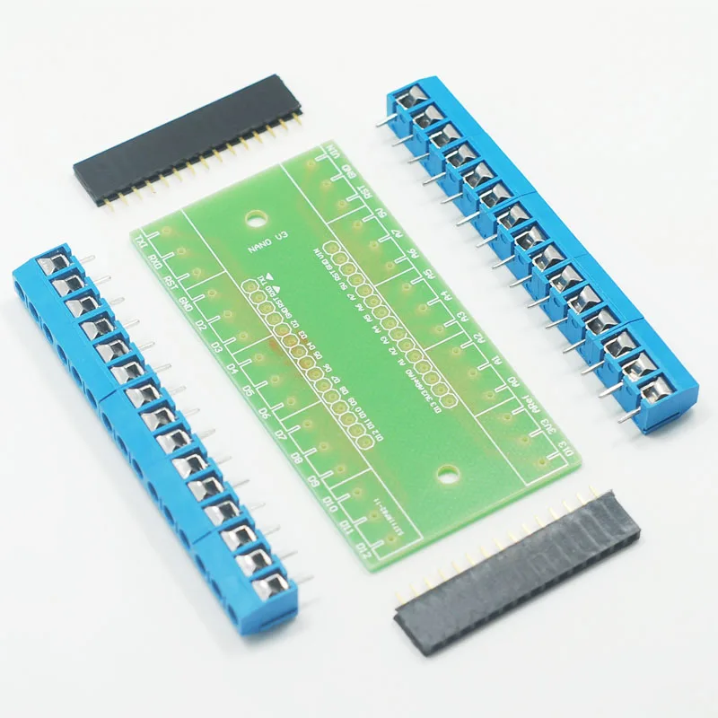
Kentucky Architecture, Nanoprocessors, & Nanocontrollers
Back in 1992/1993, we developed a technique that allows arbitrary MIMD programs to be converted into pure SIMD code. At the time, we viewed it primarily as a novel way to obtain some additional functionality from a SIMD supercomputer -- literally allowing us to program our 16,384 processing element MasPar MP-1 using a shared memory MIMD model while achieving a significant fraction of peak native (distributed memory SIMD) performance. Now, we realize it is actually a fundamentally different model of computation. Von Neuman Architecture places code and data in the same memory system; Harvard Architecture places code and data in separate but similar memory systems; what one might now call "Kentucky Architecture" places data in memory and factors out code, implementing control entirely by selection. The point is that a fully programmable processor can be made very small using this model: small enough to be used anywhere, even to add fully-programmable intelligence to micrometer-scale devices fabricated using nanotechnology. Kentucky Architecture is really nothing more than fairly conventional SIMD (Single Instruction Multiple Data) hardware combined with compiler technology that efficiently maps MIMD (Multiple Instruction Multiple Data) program states into code that can be efficiently executed by a SIMD machine, right? Thus, we expect some criticism along the lines that Kentucky Architecture is just SIMD... but it isn't. The core concept of Kentucky Architecture is selection; SIMD-style hardware is just one way in which selection can be implemented. In fact, the nanocontroller design we favor, KITE (Kentucky If-Then-Else), isn't a traditional SIMD because the control unit isn't able to function as a uniprocessor and there is VLIW (Very Long Instruction Word) style multi-way branch support. There are many other ways to build parallel hardware using selection, and the Kentucky Architecture model is even effective for analysis of conventional MIMD programs and execution.
What Must A Nanocontroller
Be Able To Do?
Minimal circuit complexity
Predictable realtime
behavior
Localized analog & digital I/O
Coordination as a PE in a parallel computer
Each nanocontroller independently
programmable (MIMD parallelism)
Reprogramability
What Architecture
Can Do All That?
No previous model... SIMD is closest
MIMDonSIMD
technology, circa 1992:
MetaState
Conversion (MSC)
Common Subexpression Induction (CSI)
Worked for MasPar MP1 supercomputer,
but significance not appreciated...
===== 4047 MA THE EL EXCITATION ROVEN MATIC INTEG MENTALITY =====
[ ] I'm here to testify about the great work Dr Osebor did for me. I have been suffering from (HERPES) disease for the past 5 years and had constant pain, especially in my knees. During the first year,I had faith in God that i would be healed someday.This disease started circulating all over my body and i have been taking treatment from my doctor, few weeks ago I came across a testimony of one lady on the internet testifying about a Man called Dr Osebor on how he cured her from HIV Virus. And she also gave the email address of this man and advise anybody to contact Dr Osebor for help for any kind of sickness that he would be of help, so I emailed him on ( oseborwinbacktemple@gmail.com ) telling him about my (HERPES Virus) he told me not to worry that i was going to be cured!! Well i never believed it,, well after all the procedures and remedy given to me by this man few weeks later i started experiencing changes all over me as Dr Osebor assured me that i will be cured,after some time i went to my doctor to confirmed if i have be finally healed behold it was TRUE, So
BalasHapus- [ ] friends my advise is if you have such sickness or any other at all you can contact Dr Osebor via email. { oseborwinbacktemple@gmail.com }or call or what sapp him on( +2348073245515 )
- [ ] DR osebor CAN AS WELL CURE THE FOLLOWING DISEASE:-
- [ ] HIV/AIDS
- [ ] HERPES
- [ ] CANCER
- [ ] ALS
- [ ] cancer
- [ ] Diabetes
eye problem etc.