
Using Game Theory in Electronics Area
Researcher applying game theory to identify electronic election tampering
The election process lies at the heart of free and open political
societies, allowing citizens to elect their leaders and in many cases
directly influence the laws that are written and enforced. Free, open,
and honest elections are therefore vital, and election tampering and
fraud have been concerns for as long as elections have been held.
Today, electronic voting machines have opened up a new avenue for
subverting elections, one that trades outward physical violence for
hidden attacks that can be just as damaging. In response, one researcher
is using game theory to develop an algorithm that can identify
potential tampering .
As a gaming theory expert, We working on developing an
algorithm that can monitor voting machines during the election process
or audit them afterward and prior to certification.
theory suggests that anyone looking to subvert an election would be
careful to target only individual machines or those placed in specific
districts, creating near ties in those districts where the opposition’s
candidate would otherwise likely win the vote.
The new extension more realistically models the
attacks on voting systems that would actually happen. It’s easy enough
for humans to just work with a list of districts in order of importance
to, say, a presidential election. It’s harder to figure out how to
randomize that list to best determine which districts would be targeted.
Turns out it helps a tremendous deal to have a computer.”Essentially, the algorithm allows computers to do the tedious and labor-intensive work of pulling random districts that might be attractive for tampering and check for discrepancies. In addition, the process by which the algorithm would conduct its analysis would be unpredictable, which would be a better match for the techniques that could be used by attackers.
With game theory, you can systematically address attacks and their consequences. If there are a million people who voted illegally, you want to know that and mitigate it. How you deal with that is going to be up to the authorities, but they need to detect it first.” By using game theory and assuming the worst-case scenario of an agent that uses a similar algorithm, We hopes to cut off election tampering at the pass.
Digital Logic | Introduction of Sequential Circuits
A Sequential circuit combinational logic circuit that consists of inputs variable (X), logic gates (Computational circuit), and output variable (Z).
Combinational circuit produces an output based on input variable only, but Sequential circuit produces an output based on current input and previous input variables. That means sequential circuits include memory elements which are capable of storing binary information. That binary information defines the state of the sequential circuit at that time. A latch capable of storing one bit of information.

As shown in figure there are two types of input to the combinational logic :
- External inputs which not controlled by the circuit.
- Internal inputs which are a function of a previous output states.
Types of Sequential Circuits – There are two types of sequential circuit :
Asynchronous sequential circuit – These circuit do not use a clock signal but uses the pulses of the inputs. These circuits are faster than synchronous sequential circuits because there is clock pulse and change their state immediately when there is a change in the input signal. We use asynchronous sequential circuits when speed of operation is important and independent of internal clock pulse.

But these circuits are more difficult to design and their output is uncertain.
Synchronous sequential circuit – These circuit uses clock signal and level inputs (or pulsed) (with restrictions on pulse width and circuit propagation). The output pulse is the same duration as the clock pulse for the clocked sequential circuits. Since they wait for the next clock pulse to arrive to perform the next operation, so these circuits are bit slower compared to asynchronous. Level output changes state at the start of an input pulse and remains in that until the next input or clock pulse.

We use synchronous sequential circuit in synchronous counters, flip flops, and in the design of MOORE-MEALY state management machines.
We use sequential circuits to design Counters, Registers, RAM, MOORE/MEALY Machine and other state retaining machines.
Read-Only Memory (ROM) | Classification and Programming
Read-Only Memory (ROM) is the primary memory unit of any computer system along with the Random Access Memory (RAM), but unlike RAM, in ROM, the binary information is stored permanently . Now, this information to be stored is provided by the designer and is then stored inside the ROM . Once, it is stored, it remains within the unit, even when power is turned off and on again .
The information is embedded in the ROM, in the form of bits, by a process known as programming the ROM . Here, programming is used to refer to the hardware procedure which specifies the bits that are going to be inserted in the hardware configuration of the device . And this is what makes ROM a Programmable Logic Device (PLD) .
Programmable Logic Device
A Programmable Logic Device (PLD) is an IC (Integrated Circuit) with internal logic gates connected through electronic paths that behave similar to fuses . In the original state, all the fuses are intact, but when we program these devices, we blow away certain fuses along the paths that must be removed to achieve a particular configuration. And this is what happens in ROM, ROM consists of nothing but basic logic gates arranged in such a way that they store the specified bits.
Typically, a PLD can have hundreds to millions of gates interconnected through hundreds to thousands of internal paths . In order to show the internal logic diagram of such a device a special symbology is used, as shown below-
The first image shows the conventional way of representing inputs to a logic gate and the second symbol shows the special way of showing inputs to a logic gate, called as Array Logic Symbol, where each vertical line represents the input to the logic gate .
Structure of ROM
The block diagram for the ROM is as given below-
Block Structure
- It consists of k input lines and n output lines .
- The k input lines is used to take the input address from where we want to access the content of the ROM .
- Since each of the k input lines can be either 0 or 1, so there are 2
 total addresses which can be referred to by these input lines and each
of these addresses contain n bit information, which is given out as the
output of the ROM.
total addresses which can be referred to by these input lines and each
of these addresses contain n bit information, which is given out as the
output of the ROM. - Such a ROM is specified as 2 x n ROM .
- It consists of two basic components – Decoder and OR gates .
- A Decoder is a combinational circuit which is used to decode any encoded form ( such as binary, BCD ) to a more known form ( such as decimal form ) .
- In ROM, the input to a decoder will be in binary form and the output will represent its decimal equivalent .
- The Decoder is represented as l x 2
 , that is, it has l inputs and has 2 outputs, which implies that it will take l-bit binary number and decode it into one of the 2 decimal number .
 - All the OR gates present in the ROM will have outputs of the decoder as their input .
Classification Of ROM
Mask ROM – In this type of ROM, the specification
of the ROM (its contents and their location), is taken by the
manufacturer from the customer in tabular form in a specified format and
then makes corresponding masks for the paths to produce the desired
output . This is costly - mended, only if large quantity of the same ROM is required). Uses – They are used in network operating systems, server operating systems, storing of fonts for laser printers, sound data in electronic musical instruments .
- PROM – It stands for Programmable Read-Only Memory .
It is first prepared as blank memory, and then it is programmed to
store the information . The difference between PROM and Mask ROM is that
PROM is manufactured as blank memory and programmed after
manufacturing, whereas a Mask ROM is programmed during the manufacturing
process.
To program the PROM, a PROM programmer or PROM burner is used . The process of programming the PROM is called as burning the PROM . Also, the data stored in it cannot be modified, so it is called as one – time programmable device. Uses – They have several different applications, including cell phones, video game consoles, RFID tags, medical devices, and other electronics.
- EPROM – It stands for Erasable Programmable
Read-Only Memory . It overcomes the disadvantage of PROM that once
programmed, the fixed pattern is permanent and cannot be altered . If a
bit pattern has been established, the PROM becomes unusable, if the bit
pattern has to be changed .
This problem has been overcome by the EPROM, as when the EPROM is
placed under a special ultraviolet light for a length of time, the
shortwave radiation makes the EPROM return to its initial state, which
then can be programmed accordingly . Again for erasing the content, PROM
programmer or PROM burner is used.
Uses – Before the advent of EEPROMs, some micro-controllers, like some versions of Intel 8048, the Freescale 68HC11 used EPROM to store their program . - EEPROM – It stands for Electrically Erasable Programmable Read-Only Memory . It is similar to EPROM, except that in this, the EEPROM is returned to its initial state by application of an electrical signal, in place of ultraviolet light . Thus, it provides the ease of erasing, as this can be done, even if the memory is positioned in the computer. It erases or writes one byte of data at a time .
- Flash ROM – It is an enhanced version of EEPROM .The difference between EEPROM and Flash ROM is that in EEPROM, only 1 byte of data can be deleted or written at a particular time, whereas, in flash memory, blocks of data (usually 512 bytes) can be deleted or written at a particular time . So, Flash ROM is much faster than EEPROM . Uses – Many modern PCs have their BIOS stored on a flash memory chip, called as flash BIOS and they are also used in modems as well.
Programming the Read-Only Memory (ROM)
To understand how to program a ROM, consider a 4 x 4 ROM, which means
that it has total of 4 addresses at which information is stored, and
each of those addresses has a 4-bit information, which is permanent and
must be given as the output, when we access a particular address . The
following steps need to be performed to program the ROM –Construct a truth table, which would decide the content of each address of the ROM and based upon which a particular ROM will be programmed. So, the truth table for the specification of the 4 x 4 ROM is described as below :
This truth table shows that at location 00, content to be stored is 0011, at location 01, the content should be 1100, and so on, such that whenever a particular address is given as input, the content at that particular address is fetched . Since, with 2 input bits, 4 input combinations are possible and each of these combinations hold a 4-bit information, so this ROM is a 4 X 4 ROM
Now, based upon the total no. of addresses in the ROM and the length of their content, decide the decoder as well as the no. of OR gates to be used .
Generally, for a 2
x n ROM, a k x 2 decoder is used, and the total no. of OR gates is equal to the total no. of bits stored at each location in the ROM .So, in this case, for a 4 x 4 ROM, the decoder to be used is a 2 x 4 decoder.
The following is a 2 x 4 decoder –
The truth table for a 2 x 4 decoder is as follows –
When both the inputs are 0, then only D
 is 1 and rest are 0, when input is 01, then, only D
 is high and so on. (Just remember that if the input combination of the
decoder resolves to a particular decimal number d, then at the output
side the terminal which is at position d + 1 from the top will be 1 and
rest will be 0).
is high and so on. (Just remember that if the input combination of the
decoder resolves to a particular decimal number d, then at the output
side the terminal which is at position d + 1 from the top will be 1 and
rest will be 0).Now, since we want each address to store 4 – bits in the 4 x 4 ROM, so, there will be 4 OR gates, with each of the 4 outputs of the decoder being input to each one of the 4 OR gates, whose output will be the output of the ROM, as follows –
A cross sign in this figure shows connection between the two lines is intact . Now, since there are 4 OR gates and 4 output lines from the decoder, so there are total of 16 intersections, called as crosspoint .
Now, program the intersection between the two lines, as per the truth table, so that the output of the ROM ( OR gates ) is in accordance with the truth table .
For programming the crosspoints, initially all the crosspoints are left intact, which means that it is logically equivalent to a closed switch, but these intact connections can be blown by the application of a high – voltage pulse into these fuse, which will disconnect the two interconnected lines, and in this way the output of a ROM can be manipulated .
So, to program a ROM, just look at the truth table specifying the ROM and blow away (if required) a connection . The connections for the 4 x 4 ROM as per the truth table is as shown below –
Remember, a cross sign is used to denote that the connection is left intact and if there is no cross this means that there is no connection .
In this figure, since, as can be seen from the truth table specifying the ROM, when the input is 00, then, the output is 0011, so as we know from the truth table of a decoder, that input 00 gives output such that only D
is 1 and rest are 0, so to get output 0011 from the OR gates, the connections of D
with the first two OR gates has been blown away, to get the outputs as
0, while the last two OR gates give the output as 1, which is what is
required . Similarly, when the input is 01, then the output should be 1100, and with input 01, in decoder only D
is 1 and rest are 0, so to get the desired output the first two OR gates have their connection intact with D, while last two OR gates have their connection blown away . And for the rest also the same procedure is followed .So, this is how a ROM is programmed and since, the output of these gates will remain constant everytime, so that is how the information is stored permanently in the ROM, and does not get altered even on switching on and off .
Game theory
+++++++++++++++++++++++++++++++++++++++++++++++++++++++++++++++++++++++
Modern game theory began with the idea regarding the existence of mixed-strategy equilibrium in two-person zero-sum games and its proof by John von Neumann. Von Neumann's original proof used the Brouwer fixed-point theorem on continuous mappings into compact convex sets, which became a standard method in game theory and mathematical.
A game is cooperative if the players are able to form binding commitments externally enforced (e.g. through contract law). A game is non-cooperative if players cannot form alliances or if all agreements need to be self-enforcing (e.g. through credible threats).
Cooperative games are often analysed through the framework of cooperative game theory, which focuses on predicting which coalitions will form, the joint actions that groups take and the resulting collective payoffs. It is opposed to the traditional non-cooperative game theory which focuses on predicting individual players' actions and payoffs and analyzing Nash equilibria.Cooperative game theory provides a high-level approach as it only describes the structure, strategies and payoffs of coalitions, whereas non-cooperative game theory also looks at how bargaining procedures will affect the distribution of payoffs within each coalition. As non-cooperative game theory is more general, cooperative games can be analyzed through the approach of non-cooperative game theory (the converse does not hold) provided that sufficient assumptions are made to encompass all the possible strategies available to players due to the possibility of external enforcement of cooperation. While it would thus be optimal to have all games expressed under a non-cooperative framework, in many instances insufficient information is available to accurately model the formal procedures available to the players during the strategic bargaining process, or the resulting model would be of too high complexity to offer a practical tool in the real world. In such cases, cooperative game theory provides a simplified approach that allows analysis of the game at large without having to make any assumption about bargaining powers.
Symmetric / Asymmetric
| E | F | |
| E | 1, 2 | 0, 0 |
| F | 0, 0 | 1, 2 |
| An asymmetric game | ||
Most commonly studied asymmetric games are games where there are not identical strategy sets for both players. For instance, the ultimatum game and similarly the dictator game have different strategies for each player. It is possible, however, for a game to have identical strategies for both players, yet be asymmetric. For example, the game pictured to the right is asymmetric despite having identical strategy sets for both players.
Zero-sum / Non-zero-sum
| A | B | |
| A | –1, 1 | 3, –3 |
| B | 0, 0 | –2, 2 |
| A zero-sum game | ||
Many games studied by game theorists (including the famed prisoner's dilemma) are non-zero-sum games, because the outcome has net results greater or less than zero. Informally, in non-zero-sum games, a gain by one player does not necessarily correspond with a loss by another.
Constant-sum games correspond to activities like theft and gambling, but not to the fundamental economic situation in which there are potential gains from trade. It is possible to transform any game into a (possibly asymmetric) zero-sum game by adding a dummy player (often called "the board") whose losses compensate the players' net winnings.
Simultaneous / Sequential
Simultaneous games are games where both players move simultaneously, or if they do not move simultaneously, the later players are unaware of the earlier players' actions (making them effectively simultaneous). Sequential games (or dynamic games) are games where later players have some knowledge about earlier actions. This need not be perfect information about every action of earlier players; it might be very little knowledge. For instance, a player may know that an earlier player did not perform one particular action, while s/he does not know which of the other available actions the first player actually performed.The difference between simultaneous and sequential games is captured in the different representations discussed above. Often, normal form is used to represent simultaneous games, while extensive form is used to represent sequential ones. The transformation of extensive to normal form is one way, meaning that multiple extensive form games correspond to the same normal form. Consequently, notions of equilibrium for simultaneous games are insufficient for reasoning about sequential games; see subgame perfection.
In short, the differences between sequential and simultaneous games are as follows:
| Sequential | Simultaneous | |
|---|---|---|
| Normally denoted by | Decision trees | Payoff matrices |
Prior knowledge
of opponent's move? |
Yes | No |
| Time axis? | Yes | No |
| Also known as |
Extensive-form game
Extensive game |
Strategy game
Strategic game |
Perfect information and imperfect information

A game of imperfect information (the dotted line represents ignorance on the part of player 2, formally called an information set)
Many card games are games of imperfect information, such as poker and bridge. Perfect information is often confused with complete information, which is a similar concept.Complete information requires that every player know the strategies and payoffs available to the other players but not necessarily the actions taken. Games of incomplete information can be reduced, however, to games of imperfect information by introducing "moves by nature".
Combinatorial games
Games in which the difficulty of finding an optimal strategy stems from the multiplicity of possible moves are called combinatorial games. Examples include chess and go. Games that involve imperfect information may also have a strong combinatorial character, for instance backgammon. There is no unified theory addressing combinatorial elements in games. There are, however, mathematical tools that can solve particular problems and answer general questions.Games of perfect information have been studied in combinatorial game theory, which has developed novel representations, e.g. surreal numbers, as well as combinatorial and algebraic (and sometimes non-constructive) proof methods to solve games of certain types, including "loopy" games that may result in infinitely long sequences of moves. These methods address games with higher combinatorial complexity than those usually considered in traditional (or "economic") game theory. A typical game that has been solved this way is hex. A related field of study, drawing from computational complexity theory, is game complexity, which is concerned with estimating the computational difficulty of finding optimal strategies.
Research in artificial intelligence has addressed both perfect and imperfect information games that have very complex combinatorial structures (like chess, go, or backgammon) for which no provable optimal strategies have been found. The practical solutions involve computational heuristics, like alpha-beta pruning or use of artificial neural networks trained by reinforcement learning, which make games more tractable in computing practice.
Infinitely long games
Games, as studied by economists and real-world game players, are generally finished in finitely many moves. Pure mathematicians are not so constrained, and set theorists in particular study games that last for infinitely many moves, with the winner (or other payoff) not known until after all those moves are completed.The focus of attention is usually not so much on the best way to play such a game, but whether one player has a winning strategy. (It can be proven, using the axiom of choice, that there are games – even with perfect information and where the only outcomes are "win" or "lose" – for which neither player has a winning strategy.) The existence of such strategies, for cleverly designed games, has important consequences in descriptive set theory.
Discrete and continuous games
Much of game theory is concerned with finite, discrete games, that have a finite number of players, moves, events, outcomes, etc. Many concepts can be extended, however. Continuous games allow players to choose a strategy from a continuous strategy set. For instance, Cournot competition is typically modeled with players' strategies being any non-negative quantities, including fractional quantities.Differential games
Differential games such as the continuous pursuit and evasion game are continuous games where the evolution of the players' state variables is governed by differential equations. The problem of finding an optimal strategy in a differential game is closely related to the optimal control theory. In particular, there are two types of strategies: the open-loop strategies are found using the Pontryagin maximum principle while the closed-loop strategies are found using Bellman's Dynamic Programming method.A particular case of differential games are the games with a random time horizon. In such games, the terminal time is a random variable with a given probability distribution function. Therefore, the players maximize the mathematical expectation of the cost function. It was shown that the modified optimization problem can be reformulated as a discounted differential game over an infinite time interval.
Evolutionary game theory
Evolutionary game theory studies players who adjust their strategies over time according to rules that are not necessarily rational or farsighted. In general, the evolution of strategies over time according to such rules is modeled as a Markov chain with a state variable such as the current strategy profile or how the game has been played in the recent past. Such rules may feature imitation, optimization or survival of the fittest.In biology, such models can represent (biological) evolution, in which offspring adopt their parents' strategies and parents who play more successful strategies (i.e. corresponding to higher payoffs) have a greater number of offspring. In the social sciences, such models typically represent strategic adjustment by players who play a game many times within their lifetime and, consciously or unconsciously, occasionally adjust their strategies.
Stochastic outcomes (and relation to other fields)
Individual decision problems with stochastic outcomes are sometimes considered "one-player games". These situations are not considered game theoretical by some authors. They may be modeled using similar tools within the related disciplines of decision theory, operations research, and areas of artificial intelligence, particularly AI planning (with uncertainty) and multi-agent system. Although these fields may have different motivators, the mathematics involved are substantially the same, e.g. using Markov decision processes (MDP).Stochastic outcomes can also be modeled in terms of game theory by adding a randomly acting player who makes "chance moves" ("moves by nature"). This player is not typically considered a third player in what is otherwise a two-player game, but merely serves to provide a roll of the dice where required by the game.
For some problems, different approaches to modeling stochastic outcomes may lead to different solutions. For example, the difference in approach between MDPs and the minimax solution is that the latter considers the worst-case over a set of adversarial moves, rather than reasoning in expectation about these moves given a fixed probability distribution. The minimax approach may be advantageous where stochastic models of uncertainty are not available, but may also be overestimating extremely unlikely (but costly) events, dramatically swaying the strategy in such scenarios if it is assumed that an adversary can force such an event to happen. ( Black swan theory for more discussion on this kind of modeling issue, particularly as it relates to predicting and limiting losses in investment banking.)
General models that include all elements of stochastic outcomes, adversaries, and partial or noisy observability (of moves by other players) have also been studied. The "gold standard" is considered to be partially observable stochastic game (POSG), but few realistic problems are computationally feasible in POSG representation.
Metagames
These are games the play of which is the development of the rules for another game, the target or subject game. Metagames seek to maximize the utility value of the rule set developed. The theory of metagames is related to mechanism design theory.The term metagame analysis is also used to refer to a practical approach developed by Nigel Howard. whereby a situation is framed as a strategic game in which stakeholders try to realise their objectives by means of the options available to them. Subsequent developments have led to the formulation of confrontation analysis.
Pooling games
These are games prevailing over all forms of society. Pooling games are repeated plays with changing payoff table in general over an experienced path and their equilibrium strategies usually take a form of evolutionary social convention and economic convention. Pooling game theory emerges to formally recognize the interaction between optimal choice in one play and the emergence of forthcoming payoff table update path, identify the invariance existence and robustness, and predict variance over time. The theory is based upon topological transformation classification of payoff table update over time to predict variance and invariance, and is also within the jurisdiction of the computational law of reachable optimality for ordered system.Mean field game theory
Mean field game theory is the study of strategic decision making in very large populations of small interacting agents. This class of problems was considered in the economics literature by Boyan Jovanovic and Robert W. Rosenthal, in the engineering literature by Peter E. Caines and by mathematician Pierre-Louis Lions and Jean-Michel Lasry.Representation of games
The games studied in game theory are well-defined mathematical objects. To be fully defined, a game must specify the following elements: the players of the game, the information and actions available to each player at each decision point, and the payoffs for each outcome. (Eric Rasmusen refers to these four "essential elements" by the acronym "PAPI".) A game theorist typically uses these elements, along with a solution concept of their choosing, to deduce a set of equilibrium strategies for each player such that, when these strategies are employed, no player can profit by unilaterally deviating from their strategy. These equilibrium strategies determine an equilibrium to the game—a stable state in which either one outcome occurs or a set of outcomes occur with known probability.Most cooperative games are presented in the characteristic function form, while the extensive and the normal forms are used to define noncooperative games.
Extensive form

An extensive form game
The game pictured consists of two players. The way this particular game is structured (i.e., with sequential decision making and perfect information), Player 1 "moves" first by choosing either F or U (Fair or Unfair). Next in the sequence, Player 2, who has now seen Player 1's move, chooses to play either A or R. Once Player 2 has made his/ her choice, the game is considered finished and each player gets their respective payoff. Suppose that Player 1 chooses U and then Player 2 chooses A: Player 1 then gets a payoff of "eight" (which in real-world terms can be interpreted in many ways, the simplest of which is in terms of money but could mean things such as eight days of vacation or eight countries conquered or even eight more opportunities to play the same game against other players) and Player 2 gets a payoff of "two".
The extensive form can also capture simultaneous-move games and games with imperfect information. To represent it, either a dotted line connects different vertices to represent them as being part of the same information set (i.e. the players do not know at which point they are), or a closed line is drawn around them.
Normal form
| Player 2 chooses Left |
Player 2 chooses Right | |
| Player 1 chooses Up |
4, 3 | –1, –1 |
| Player 1 chooses Down |
0, 0 | 3, 4 |
| Normal form or payoff matrix of a 2-player, 2-strategy game | ||
When a game is presented in normal form, it is presumed that each player acts simultaneously or, at least, without knowing the actions of the other. If players have some information about the choices of other players, the game is usually presented in extensive form.
Every extensive-form game has an equivalent normal-form game, however the transformation to normal form may result in an exponential blowup in the size of the representation, making it computationally impractical.
Characteristic function form
In games that possess removable utility, separate rewards are not given; rather, the characteristic function decides the payoff of each unity. The idea is that the unity that is 'empty', so to speak, does not receive a reward at all.The origin of this form is to be found in John von Neumann and Oskar Morgenstern's book; when looking at these instances, they guessed that when a union
 appears, it works against the fraction
 as if two individuals were playing a normal game. The balanced payoff of
C is a basic function. Although there are differing examples that help
determine coalitional amounts from normal games, not all appear that in
their function form can be derived from such.
as if two individuals were playing a normal game. The balanced payoff of
C is a basic function. Although there are differing examples that help
determine coalitional amounts from normal games, not all appear that in
their function form can be derived from such.
Formally, a characteristic function is seen as: (N,v), where N represents the group of people and
 is a normal utility.
Such characteristic functions have expanded to describe games where there is no removable utility.
General and applied uses
As a method of applied mathematics, game theory has been used to study a wide variety of human and animal behaviors. It was initially developed in economics to understand a large collection of economic behaviors, including behaviors of firms, markets, and consumers. The first use of game-theoretic analysis was by Antoine Augustin Cournot in 1838 with his solution of the Cournot duopoly. The use of game theory in the social sciences has expanded, and game theory has been applied to political, sociological, and psychological behaviors as well.Although pre-twentieth century naturalists such as Charles Darwin made game-theoretic kinds of statements, the use of game-theoretic analysis in biology began with Ronald Fisher's studies of animal behavior during the 1930s. This work predates the name "game theory", but it shares many important features with this field. The developments in economics were later applied to biology largely by John Maynard Smith in his book Evolution and the Theory of Games.
In addition to being used to describe, predict, and explain behavior, game theory has also been used to develop theories of ethical or normative behavior and to prescribe such behavior. In economics and philosophy, scholars have applied game theory to help in the understanding of good or proper behavior. Game-theoretic arguments of this type can be found as far back as Plato.
Description and modeling

A four-stage centipede game
Some game theorists, following the work of John Maynard Smith and George R. Price, have turned to evolutionary game theory in order to resolve these issues. These models presume either no rationality or bounded rationality on the part of players. Despite the name, evolutionary game theory does not necessarily presume natural selection in the biological sense. Evolutionary game theory includes both biological as well as cultural evolution and also models of individual learning (for example, fictitious play dynamics).
Prescriptive or normative analysis
| Cooperate | Defect | |
| Cooperate | -1, -1 | -10, 0 |
| Defect | 0, -10 | -5, -5 |
| The Prisoner's Dilemma | ||
Economics and business
Game theory is a major method used in mathematical economics and business for modeling competing behaviors of interacting agents. Applications include a wide array of economic phenomena and approaches, such as auctions, bargaining, mergers & acquisitions pricing, fair division, duopolies, oligopolies, social network formation, agent-based computational economics, general equilibrium, mechanism design, and voting systems; and across such broad areas as experimental economics, behavioral economics, information economics,industrial organization, and political economy.This research usually focuses on particular sets of strategies known as "solution concepts" or "equilibria". A common assumption is that players act rationally. In non-cooperative games, the most famous of these is the Nash equilibrium. A set of strategies is a Nash equilibrium if each represents a best response to the other strategies. If all the players are playing the strategies in a Nash equilibrium, they have no unilateral incentive to deviate, since their strategy is the best they can do given what others are doing.[50][51]
The payoffs of the game are generally taken to represent the utility of individual players.
A prototypical paper on game theory in economics begins by presenting a game that is an abstraction of a particular economic situation. One or more solution concepts are chosen, and the author demonstrates which strategy sets in the presented game are equilibria of the appropriate type. Naturally one might wonder to what use this information should be put. Economists and business professors suggest two primary uses (noted above): descriptive and prescriptive.
Political science
The application of game theory to political science is focused in the overlapping areas of fair division, political economy, public choice, war bargaining, positive political theory, and social choice theory. In each of these areas, researchers have developed game-theoretic models in which the players are often voters, states, special interest groups, and politicians.Early examples of game theory applied to political science are provided by Anthony Downs. In his book An Economic Theory of Democracy,[52] he applies the Hotelling firm location model to the political process. In the Downsian model, political candidates commit to ideologies on a one-dimensional policy space. Downs first shows how the political candidates will converge to the ideology preferred by the median voter if voters are fully informed, but then argues that voters choose to remain rationally ignorant which allows for candidate divergence. Game Theory was applied in 1962 to the Cuban missile crisis during the presidency of John F. Kennedy.
It has also been proposed that game theory explains the stability of any form of political government. Taking the simplest case of a monarchy, for example, the king, being only one person, does not and cannot maintain his authority by personally exercising physical control over all or even any significant number of his subjects. Sovereign control is instead explained by the recognition by each citizen that all other citizens expect each other to view the king (or other established government) as the person whose orders will be followed. Coordinating communication among citizens to replace the sovereign is effectively barred, since conspiracy to replace the sovereign is generally punishable as a crime. Thus, in a process that can be modeled by variants of the prisoner's dilemma, during periods of stability no citizen will find it rational to move to replace the sovereign, even if all the citizens know they would be better off if they were all to act collectively.
A game-theoretic explanation for democratic peace is that public and open debate in democracies send clear and reliable information regarding their intentions to other states. In contrast, it is difficult to know the intentions of nondemocratic leaders, what effect concessions will have, and if promises will be kept. Thus there will be mistrust and unwillingness to make concessions if at least one of the parties in a dispute is a non-democracy.
On the other hand, game theory predicts that two countries may still go to war even if their leaders are cognizant of the costs of fighting. War may result from asymmetric information; two countries may have incentives to mis-represent the amount of military resources they have on hand, rendering them unable to settle disputes agreeably without resorting to fighting. Moreover, war may arise because of commitment problems: if two countries wish to settle a dispute via peaceful means, but each wishes to go back on the terms of that settlement, they may have no choice but to resort to warfare. Finally, war may result from issue indivisibilities.
Game theory could also help predict a nation's responses when there is a new rule or law to be applied to that nation. One example would be Peter John Wood's (2013) research when he looked into what nations could do to help reduce climate change. Wood thought this could be accomplished by making treaties with other nations to reduce green house gas emissions. However, he concluded that this idea could not work because it would create a prisoner's dilemma to the nations.
Biology
| Hawk | Dove | |
| Hawk | 20, 20 | 80, 40 |
| Dove | 40, 80 | 60, 60 |
| The hawk-dove game | ||
In biology, game theory has been used as a model to understand many different phenomena. It was first used to explain the evolution (and stability) of the approximate 1:1 sex ratios. (Fisher 1930) suggested that the 1:1 sex ratios are a result of evolutionary forces acting on individuals who could be seen as trying to maximize their number of grandchildren.
Additionally, biologists have used evolutionary game theory and the ESS to explain the emergence of animal communication.[58] The analysis of signaling games and other communication games has provided insight into the evolution of communication among animals. For example, the mobbing behavior of many species, in which a large number of prey animals attack a larger predator, seems to be an example of spontaneous emergent organization. Ants have also been shown to exhibit feed-forward behavior akin to fashion (see Paul Ormerod's Butterfly Economics)
Biologists have used the game of chicken to analyze fighting behavior and territoriality.
According to Maynard Smith, in the preface to Evolution and the Theory of Games, "paradoxically, it has turned out that game theory is more readily applied to biology than to the field of economic behaviour for which it was originally designed". Evolutionary game theory has been used to explain many seemingly incongruous phenomena in nature.
One such phenomenon is known as biological altruism. This is a situation in which an organism appears to act in a way that benefits other organisms and is detrimental to itself. This is distinct from traditional notions of altruism because such actions are not conscious, but appear to be evolutionary adaptations to increase overall fitness. Examples can be found in species ranging from vampire bats that regurgitate blood they have obtained from a night's hunting and give it to group members who have failed to feed, to worker bees that care for the queen bee for their entire lives and never mate, to vervet monkeys that warn group members of a predator's approach, even when it endangers that individual's chance of survival. All of these actions increase the overall fitness of a group, but occur at a cost to the individual.
Evolutionary game theory explains this altruism with the idea of kin selection. Altruists discriminate between the individuals they help and favor relatives. Hamilton's rule explains the evolutionary rationale behind this selection with the equation c < b × r, where the cost c to the altruist must be less than the benefit b to the recipient multiplied by the coefficient of relatedness r. The more closely related two organisms are causes the incidences of altruism to increase because they share many of the same alleles. This means that the altruistic individual, by ensuring that the alleles of its close relative are passed on through survival of its offspring, can forgo the option of having offspring itself because the same number of alleles are passed on. For example, helping a sibling (in diploid animals) has a coefficient of ½, because (on average) an individual shares ½ of the alleles in its sibling's offspring. Ensuring that enough of a sibling's offspring survive to adulthood precludes the necessity of the altruistic individual producing offspring. The coefficient values depend heavily on the scope of the playing field; for example if the choice of whom to favor includes all genetic living things, not just all relatives, we assume the discrepancy between all humans only accounts for approximately 1% of the diversity in the playing field, a co-efficient that was ½ in the smaller field becomes 0.995. Similarly if it is considered that information other than that of a genetic nature (e.g. epigenetics, religion, science, etc.) persisted through time the playing field becomes larger still, and the discrepancies smaller.
Computer science and logic
Game theory has come to play an increasingly important role in logic and in computer science. Several logical theories have a basis in game semantics. In addition, computer scientists have used games to model interactive computations. Also, game theory provides a theoretical basis to the field of multi-agent systems.Separately, game theory has played a role in online algorithms; in particular, the k-server problem, which has in the past been referred to as games with moving costs and request-answer games. Yao's principle is a game-theoretic technique for proving lower bounds on the computational complexity of randomized algorithms, especially online algorithms.
The emergence of the internet has motivated the development of algorithms for finding equilibria in games, markets, computational auctions, peer-to-peer systems, and security and information markets. Algorithmic game theory and within it algorithmic mechanism design combine computational algorithm design and analysis of complex systems with economic theory .
Philosophy
| Stag | Hare | |
| Stag | 3, 3 | 0, 2 |
| Hare | 2, 0 | 2, 2 |
| Stag hunt | ||
Game theory has also challenged philosophers to think in terms of interactive epistemology: what it means for a collective to have common beliefs or knowledge, and what are the consequences of this knowledge for the social outcomes resulting from the interactions of agents. Philosophers who have worked in this area include Bicchieri (1989, 1993), Skyrms (1990), and Stalnaker (1999).
In ethics, some (most notably David Gauthier, Gregory Kavka, and Jean Hampton) authors have attempted to pursue Thomas Hobbes' project of deriving morality from self-interest. Since games like the prisoner's dilemma present an apparent conflict between morality and self-interest, explaining why cooperation is required by self-interest is an important component of this project. This general strategy is a component of the general social contract view in political philosophy (for examples, see Gauthier (1986) and Kavka (1986)).
Other authors have attempted to use evolutionary game theory in order to explain the emergence of human attitudes about morality and corresponding animal behaviors. These authors look at several games including the prisoner's dilemma, stag hunt, and the Nash bargaining game as providing an explanation for the emergence of attitudes about morality
Game theory
Game theory is a branch of applied
mathematics and economics that studies situations where players choose
different actions in an attempt to maximize their returns.
First developed as a tool for understanding
economic behavior and then by the RAND Corporation to define nuclear
strategies, game theory is now used in many diverse academic fields,
ranging from biology and psychology to sociology and philosophy.
Beginning in the 1970s, game theory has been applied to animal behavior, including species' development by natural selection.
Because of games like the prisoner's dilemma, in which rational self-interest hurts everyone, game theory has been used in political science, ethics and philosophy.
Finally, game theory has recently drawn attention from computer scientists because of its use in artificial intelligence and cybernetics.

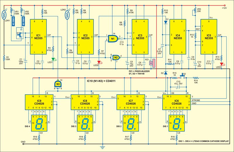
XO___XO Electronic scoring game theory to explain
to explain the principles of electronic scoring game. The principle is
simple but effective. For you to more effectively grasp this principle,
we recommend that you read the text combines schematic. This circuit
consists of a timer IC , two decade counters and a display driver along
with a 7-segment display. This game is very simple. As described above,
this is a game score score 100 and competitors quickly (in a short
step) is the winner. Score a selected one of the switches S2 and S3
pressing. The switch S2, when the pressure, the counting direction of
the counter, and the switch S3 to help count down. To start a new game,
and this is a fresh move, even if you must press switch S1 to reset the
circuit. Thereafter, press any of the two switches, ie. S2 or S3. In
pressing switch S2 and S3, the counter output changes very rapidly, BCD
when you release the switch, the final figure is still locked in the
output of IC2. The BCD number is input BCD 7 segment decoder / driver
IC3 common anode display driver DIS1. However, you can read this number
only when you press the switch S4. The order of operation between
playing games that two players "X" and "Y", is summarized as follows:
1.
Players? X? First instantaneous pressure followed by the reset switch
S1 and S2 switch either released or S3. He then press the switch S4 to
read the display (score) and notes down this number (eg X1) manually.
2.
Players "Y" is started by pressing the switch S1 followed by momentary
switches S2 and S3, and that of his fraction (say yen), after pressing
the switch S4, in the same way entirely by the first player.
3.
Player "X" and then switches S1 and repeat the steps shown in step 1,
and notes down over his new score (say, X2). He added that this score,
his previous scores. Repeat the same steps by the players "Y" in his
turn.
4. Race to the total score of the two players up to or more than 100, was declared the winner.
Several
players can participate in this game, each have the opportunity to
score in his own turn. Assembly can be by using a multifunction board.
Solving Display (light-emitting diodes and 7-segment display) on the
cabinet with three switches. Supply voltage of 5 v circuits. You can
play this game alone or with your friends.

Electronic Scoring Game
Analog to Digital Converter
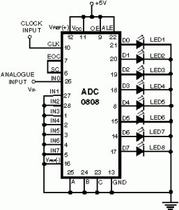
Normally
analogue-to-digital con-verter (ADC) needs interfacing
through a microprocessor to convert analogue data
into digital format. This requires hardware and
necessary software, resulting in increased
complexity and hence the total cost.
The
circuit of A-to-D converter shown here is
configured around ADC 0808, avoiding the use
of a microprocessor. The ADC 0808 is an 8-bit A-to-D
converter, having data lines D0-D7. It works on the
principle of successive approximation. It has a total
of eight analogue input channels, out of which any
one can be selected using address lines A, B
and C. Here, in this case, input channel IN0
is selected by grounding A, B and C address
lines.
Usually the control signals EOC (end of
conversion), SC (start conversion), ALE
(address latch enable) and OE (output enable) are interfaced
by means of a microprocessor. However, the circuit shown
here is built to operate in its continuous
mode without using any microprocessor.
Therefore the input control signals ALE and
OE, being active-high, are tied to Vcc (+5
volts). The input control signal SC, being active-low,
initiates start of conversion at falling edge of the
pulse, whereas the output signal EOC becomes high after
completion of digitisation. This EOC output is
coupled to SC input, where falling edge of
EOC output acts as SC input to direct the ADC
to start the conversion.
As the conversion starts, EOC signal goes high.
At next clock pulse EOC output again goes low,
and hence SC is enabled to start the next
conversion. Thus, it provides continuous 8-bit
digital output corresponding to instantaneous
value of analogue input. The maximum level of analogue
input voltage should be appropriately scaled down below
positive reference (+5V) level.
The ADC 0808 IC requires clock signal of
typically 550 kHz, which can be easily derived
from an astable multivibrator constructed
using 7404 inverter gates. In order to visualise the
digital output, the row of eight LEDs (LED1 through
LED8) have been used, wherein each LED is connected
to respective data lines D0 through D7. Since ADC
works in the continuous mode, it displays
digital output as soon as analogue input is
applied. The decimal equivalent digital output
value D for a given analogue input voltage
Vin can be calculated from the relationship .

MULTIMETER
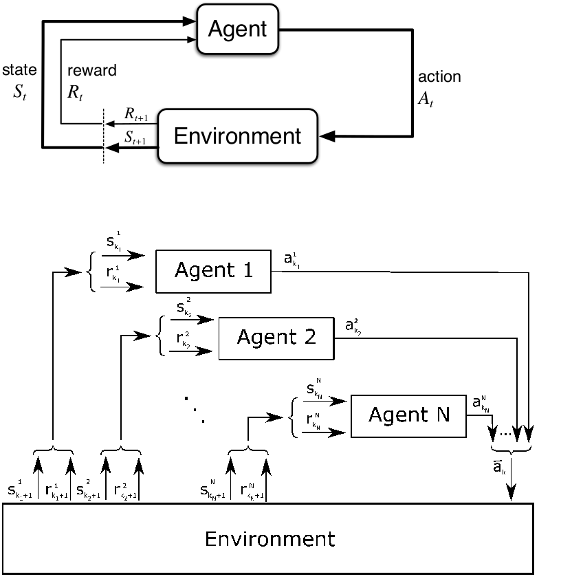
Modern Game Theory and Multi-Agent Reinforcement Learning Systems
Most
artificial intelligence(AI) systems nowadays are based on a single agent
tackling a task or, in the case of adversarial models, a couple of
agents that compete against each other to improve the overall behavior
of a system. However, many cognition problems in the real world are the
result of knowledge built by large groups of people. Take for example a
self-driving car scenario, the decisions of any agent are the result of
the behavior of many other agents in the scenario. Many scenarios in
financial markets or economics are also the result of coordinated
actions between large groups of entities. How can we mimic that behavior
in artificial intelligence(AI) agents?
Multi-Agent
Reinforcement Learning(MARL) is the deep learning discipline that
focuses on models that include multiple agents that learn by dynamically
interacting with their environment. While in single-agent reinforcement
learning scenarios the state of the environment changes solely as a
result of the actions of an agent, in MARL scenarios the environment is
subjected to the actions of all agents. From that perspective, is we
think of a MARL environment as a tuple {X1-A1,X2-A2….Xn-An} where Xm is
any given agent and Am is any given action, then the new state of the
environment is the result of the set of joined actions defined by
A1xA2x….An. In other words, the complexity of MARL scenarios increases
with the number of agents in the environment.
Another
added complexity of MARL scenarios is related to the behavior of the
agents. In many scenarios, agents in a MARL model can acts
cooperatively, competitively or exhibit neutral behaviors. To handle
those complexities, MARL techniques borrow some ideas from game theory
which can be very helpful when comes to model environments with multiple
participants. Specifically, most of MARL scenarios can be represented
using one of the following game models:
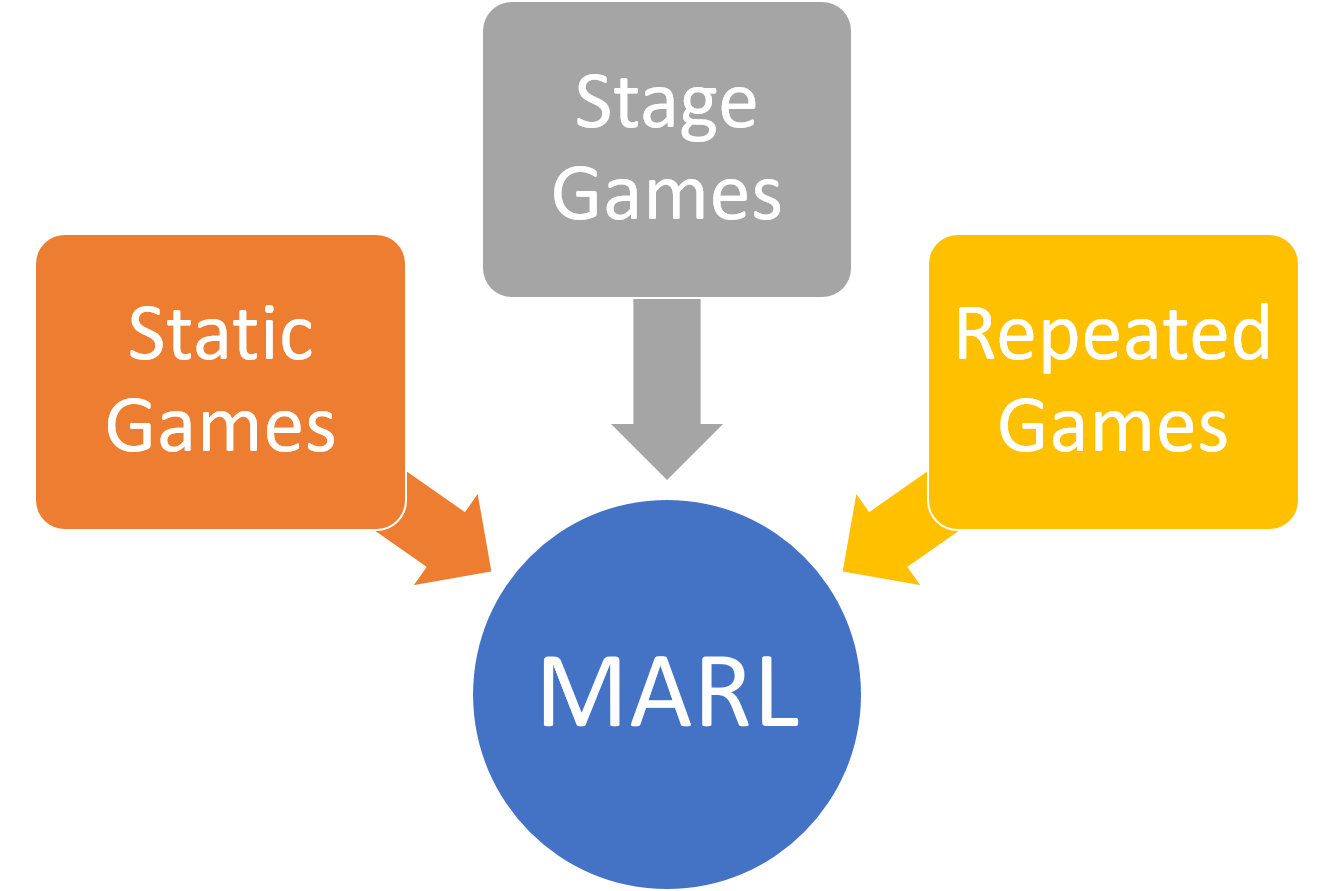
· Static Games: A
static game is one in which all players make decisions (or select a
strategy) simultaneously, without knowledge of the strategies that are
being chosen by other players. Even though the decisions may be made at
different points in time, the game is simultaneous because each player
has no information about the decisions of others; thus, it is as if the
decisions are made simultaneously.
· Stage Games: A
Stage Game is a game that arises in certain stage of a static game. In
other words, the rules of the games depend on the specific stage. The
prisoner’s dilemma is a classic example of stage game
· Repeated Games: When
players interact by playing a similar stage game (such as the
prisoner’s dilemma) numerous times, the game is called a repeated game.
Unlike a game played once, a repeated game allows for a strategy to be
contingent on past moves, thus allowing for reputation effects and
retribution.
Most
MARL scenarios can be modeled as static, stage or repeated games. New
fields in game theory such as mean-field games are becoming extremely
valuable in MARL scenarios (more about that in a future post).
MARL Algorithms and Game Theory
Recently,
we have seen an explosion in the number of MARL algorithms produced in
research labs. Keeping up with all that research is really hard but here
we can also used a some game theory ideas. One of the best taxonomies
I’ve seen to understand the MARL space, is by classifying the behavior
of agents as fully-cooperative, fully-competitive or mixed. Below is a
quick breakdown of the MARL space using that classification criteria.
To
that level, we can add another interesting classification criteria is
based on the type of task the agents in a MARL system need to perform.
For instance, in some MARL environments, agents make decisions in
complete isolation of other agents while, in other cases, they
coordinate with cooperators or competitors.
Challenges of MARL Agents
MARL
models offer tangible benefits to deep learning tasks given that they
are the closet representations of many cognitive activities in the real
world. However, there are plenty of challenges to consider when
implementing this type of models. Without trying to provide an
exhaustive list, there are three challenges that should be top of mind
of any data scientists when considering implementing MARL models:
1. The Curse of Dimensionality: The famous challenge of deep learning systems
is particularly relevant in MARL models. Many MARL strategies that work
on certain game-environments terribly fail as the number of
agents/players increase.
2. Training:
Coordinating training across a large number of agents is another
nightmare in MARL scenarios. Typically, MARL models use some training
policy coordination mechanisms to minimize the impact of the training
tasks.
3. Ambiguity:
MARL models are very vulnerable to agent ambiguity scenarios. Imagine a
multi-player game in which two agents occupied the exact same position
in the environment. To handle those challenges, the policy of each
agents needs to take into account the actions taken by other agents.
MARL
models are called to become of the most relevant deep learning
disciplines in the next decade. As these models tackle more complex
scenarios, we are likely to see more ideas from game theory become
foundational to MARL scenarios.
Reinforcement learning is the problem faced by an agent that must learn
behaviour through trial-and-error interactions with a dynamic
environment. In a multi-agent setting, the problem is often further
complicated by the need to take into account t he behaviour of other
agents in order to learn to perform effectively. Issues of coordina tion
nd cooperation must be addressed; in general, it is not sufficient for
each agent to a c selfishly in order to arrive at a globally optimal
strategy. In this work, we apply the Adaptive Heuristic Critic (AHC) and
Q-learning algorithms to agents in a simple artificial multi -agent
domain based on the Tileworld. We experimentally compare the performance
of the AHC a nd Q-learning algorithms to each other as well as to a
hand-coded greedy strate gy. The overall result is that AHC agents
perform better than the others, particularly when many other agents are
present or the world is dynamic. We also examine the notion of global
optimalit y in this system, and present a simple method of encouraging
agents to learn cooperative be haviour, which we call vicarious
reinforcement. The main result of this work is that agents that receive
addi tional vicarious reinforcement perform better than selfish agents,
even though the task being performed here is not inherently cooperative


Electronics Engineering
Electronic
Circuits - Analog Circuits - OpAmps, Signal Conditioning, Mixed Signal Design.
- Industrial Process Control Circuits
- Instrumentation and Measurement
- Mixed Circuits Analog with Digital
- Opamp Instrumentation Circuits
- Temperature Measurement Control
- Digital
Circuits - Logic Design, CMOS, TTL,
Counters, Timers, 555.
- Basic Digital Circuits
- Digital Timers, Counters and Clocks
- Mixed and Interface Circuits
- 555 Timer based Circuits
- Power
Electronics - SMPS, Regulated Power
Supplies, SSR, Energy.
- Microcontroller
- 8051, 8052, OpCodes, Analog and PC
Interface.
- Test
Measurement - Multi-Meters, Small Test
Tools, AVO Meters.
- Data
Interface - Virtual
Instrumentation, Device Networking.
- Custom
Projects - Process Timers, Chargers,
Analog Scanners.
- Hobby
Projects - Insulation tester, LED
Circuits and Meters.
- Theory
Tutorials - Basic Electronics,
Industrial Product Design.
- Electronic
Diagrams - Control Panels, Reference EE
Tables & Charts.
- Resources - Lists of Electronic Firms and Electronic Project Sites.


Dice with 7-Segment Display
This is a circuit for a dice with 7-segment display that can generate a random number from 0 to 9 and display it on a 7-segment LCD.
This 7 segment display dice circuit has
been realized using an astable oscillator circuit followed by a counter,
display driver and a display. Here we have used a timer NE555 as an astable oscillator with a frequency of about 100 Hz. Decade counter
IC CD4026 or CD4033 (whichever available) can be used as
counter-cum-display driver. When using CD4026, pin 14 (cascading output)
is to be left unused (open), but in case of CD4033, pin 14 serves as
lamp test pin and the same is to be grounded.
7 segment display dice circuit
The circuit uses only a handful of
components. Its power consumption is also quite low because of use of
CMOS ICs, and hence it is well suited for battery operation. In this
circuit two tactile switches S1 and S2 have been provided. While switch
S2 is used for initial resetting of the display to ‘0’, depression of S1
simulates throwing of the dice by a player.
When battery is connected to the
circuit, the counter and display section around IC2 (CD4026/4033) is
energised and the display would normally show ‘0’, as no clock input is
available. Should the display show any other decimal digit, you may
press re-set switch S2 so that display shows ‘0’ .To simulate throwing
of dice, the player has to press switch S1, briefly. This extends the
supply to the astable oscillator configured around IC1 as well as
capacitor C1 (through resistor R1), which charges to the battery
voltage. Thus even after switch S1 is released, the astable circuit
around IC1 keeps producing the clock until capacitor C1 discharges
sufficiently. Thus for duration of depression of switch S1 and discharge
of capacitor C1 thereafter, clock pulses are produced by IC1 and
applied to clock pin 1 of counter IC2, whose count advances at a
frequency of 100 Hz until C1 discharges sufficiently to deactivate IC1.
Circuit operation
When the oscillations from IC1 stop, the
last (random) count in counter IC2 can be viewed on the 7-segment
display. This count would normally lie between 0 and 6, since at the
leading edge of every 7th clock pulse, the counter is reset to zero.
This is achieved as follows.
Observe the behavior of ‘b’ segment
output in the Table. On reset, at count 0 until count 4, the segment ‘b’
output is high. At count 5 it changes to low level and remains so
during count 6. However, at start of count 7, the output goes from low
to high state. A differentiated sharp high pulse through C-R combination
of C4-R5 is applied to reset pin 15 of IC2 to reset the output to ‘0’
for a fraction of a pulse period (which is not visible on the 7-segment
display). Thus, if the clock stops at seventh count, the display will
read zero. There is a probability of one chance in seven that display
would show ‘0.’ In such a situation, the concerned player is given
another chance until the display is non-zero.
Note. Although it is
quite feasible to inhibit display of ‘0’ and advance the counter by ‘1’,
the same makes the circuit some what complex and therefore such a
modification has not been attempted.
speed checker
circuit diagram car speed checker circuit diagram speed checker for
highways project circuit diagram car speed checker with lcd display
circuit diagram circuit breaker finder .
LOGIC CIRCUIT AND SWITCHING THEORY ON GAME THEORY ELECTRONICS
Combinational Logic circuits that change state depending upon the actual signals being applied to their inputs at that time, Sequential Logic circuits have some form of inherent "Memory" built in to them and they are able to take into account their previous input state as well as those actually present, a sort of "before" and "after" is involved. They are generally termed as Two State or Bistable devices which can have their output set in either of two basic states, a logic level "1" or a logic level "0" and will remain "Latched" indefinitely in this current state or condition until some other input trigger pulse or signal is applied which will change its state once again.
Sequential Logic Circuit
 |
The word "Sequential" means that things happen in a "sequence", one after another and in Sequential Logic circuits, the actual clock signal determines when things will happen next. Simple sequential logic circuits can be constructed from standard Bistable circuits such as Flip-flops, Latches or Counters and which themselves can be made by simply connecting together NAND Gates and/or NOR Gates in a particular combinational way to produce the required sequential circuit.
Sequential Logic circuits can be divided into 3 main categories:
- 1. Clock Driven - Synchronous Circuits that are Synchronised to a specific clock signal.
- 2. Event Driven - Asynchronous Circuits that react or change state when an external event occurs.
- 3. Pulse Driven - Which is a Combination of Synchronous and Asynchronous.
Classification of Sequential Logic
 |
As
well as the two logic states mentioned above logic level "1" and logic
level "0", a third element is introduced that separates Sequential
Logic circuits from their Combinational LogicTIME. Sequential logic
circuits that return back to their original state once reset, i.e.
circuits with loops or feedback paths are said to be "Cyclic" in nature. counterparts, namely
SR Flip-Flop
An SR Flip-Flop
can be considered as a basic one-bit memory device that has two inputs,
one which will "SET" the device and another which will "RESET" the
device back to its original state and an output Q that will be either at a logic level "1" or logic "0" depending upon this Set/Reset condition. A basic NAND
Gate SR flip flop circuit provides feedback from its outputs to its
inputs and is commonly used in memory circuits to store data bits. The
term "Flip-flop" relates to the actual operation of the device, as it can be "Flipped" into one logic state or "Flopped" back into another.
The simplest way to make any basic one-bit Set/Reset SR flip-flop is to connect together a pair of cross-coupled 2-input NAND Gates to form a Set-Reset Bistable or a SR NAND Gate Latch, so that there is feedback from each output to one of the other NAND Gate inputs. This device consists of two inputs, one called the Reset, R and the other called the Set, S with two corresponding outputs Q and its inverse or complement Q as shown below.
The SR NAND Gate Latch
 |  |
The Set State
Consider the circuit shown above. If the input R is at logic level "0" (R = 0) and input S is at logic level "1" (S = 1), the NAND Gate Y has at least one of its inputs at logic "0" therefore, its output Q must be at a logic level "1" (NAND Gate principles). Output Q is also fed back to input A and so both inputs to the NAND Gate X are at logic level "1", and therefore its output Q must be at logic level "0". Again NAND gate principals. If the Reset input R changes state, and now becomes logic "1" with S remaining HIGH at logic level "1", NAND Gate Y inputs are now R = "1" and B = "0" and since one of its inputs is still at logic level "0" the output at Q remains at logic level "1" and the circuit is said to be "Latched" or "Set" with Q = "1" and Q = "0".
Reset State
In this second stable state, Q is at logic level "0", Q = "0" its inverse output Q is at logic level "1", not Q = "1", and is given by R = "1" and S = "0". As gate X has one of its inputs at logic "0" its output Q must equal logic level "1" (again NAND gate principles). Output Q is fed back to input B, so both inputs to NAND gate Y are at logic "1", therefore, Q = "0". If the set input, S now changes state to logic "1" with R remaining at logic "1", output Q still remains LOW at logic level "0" and the circuit's "Reset" state has been latched.
Truth Table for this Set-Reset Function
| State | S | R | Q | Q |
| Set | 1 | 0 | 1 | 0 |
| 1 | 1 | 1 | 0 | |
| Reset | 0 | 1 | 0 | 1 |
| 1 | 1 | 0 | 1 | |
| Invalid | 0 | 0 | 1 | 1 |
It can be seen that when both inputs S = "1" and R = "1" the outputs Q and Q can be at either logic level "1" or "0", depending upon the state of inputs S or R BEFORE this input condition existed. However, input state R = "0" and S = "0" is an undesirable or invalid condition and must be avoided because this will give both outputs Q and Q to be at logic level "1" at the same time and we would normally want Q to be the inverse of Q.
However, if the two inputs are now switched HIGH again after this
condition to logic "1", both the outputs will go LOW resulting in the
flip-flop becoming unstable and switch to an unknown data state based
upon the unbalance. This unbalance can cause one of the outputs to
switch faster than the other resulting in the flip-flop switching to
one state or the other which may not be the required state and data
corruption will exist. This unstable condition is known as its
Meta-stable state.
Then, a bistable latch is activated or Set by a logic "1" applied to its S input and deactivated or Reset by a logic "1" applied to its R.
The SR Latch is said to be in an "invalid" condition (Meta-stable) if
both the Set and Reset inputs are activated simultaneously.
As well as using NAND Gates, it is also possible to construct simple 1-bit SR Flip-flops using two NOR Gates connected the same configuration. The circuit will work in a similar way to the NAND
gate circuit above, except that the invalid condition exists when both
its inputs are at logic level "1" and this is shown below.
The NOR Gate SR Flip-flop
 |
Switch Debounce Circuits
One
practical use of this type of Set-Reset circuit is as a latch used to
help eliminate mechanical switch "Bounce". As its name implies, switch
bounce occurs when the contacts of any mechanically operated Switch,
Push-button or Keypad is operated and the internal switch contacts do
not fully close cleanly, but bounce together first before closing (or
opening) when the switch is pressed. This gives rise to a series of
pulses as long as tens of milliseconds that an electronic system or
circuit such as a digital counter may see as a series of logic pulses
instead of one long single pulse and behave incorrectly, for example, it
may register multiple counts instead of a single count. Then Set-Reset
SR Flip-flops or Bistable Latch circuits can be used to eliminate this
problem and this is shown below.
SR Bistable Switch Debounce Circuit
 |
Depending
upon the current state of the output, if the Set or Reset buttons are
depressed the output will change over in the manner described above and
any additional unwanted inputs (bounces) from the mechanical action of
the switch will have no effect on the output. When the other button is
pressed, the very first contact will cause the latch to change state,
but any additional bounces will also have no effect. The SR flip-flop
can then be RESET automatically after a short period of time, for
example 0.5 seconds, so as to register any additional and intentional
repeat inputs from the same switch contacts, for example multiple inputs
from the RETURN key.
Commonly
available IC's specifically made to overcome the problem of switch
bounce are the MAX6816, single input, MAX6817, dual input and the
MAX6818 octal input switch debouncer IC's. These chips contain the
necessary flip-flop circuitry to provide clean interfacing of mechanical
switches to digital systems.
Set-Reset
Latches can also be used as Monostable (one-shot) pulse generators to
generate a single output pulse, either High or Low, of some specified
width or time period for timing or control purposes. The 74LS279 is a
Quad SR Bistable Latch IC, which contains 4 individual NAND type bistable's within a single chip enabling switch debounce or monostable/astable clock circuits to be easily constructed.
Gated or Clocked SR Flip-Flop
It
is sometimes desirable in sequential logic circuits to have a bistable
SR flip-flop that only change state when certain conditions are met
regardless of the condition of either the Set or the Reset inputs. By connecting a 2-input NAND gate in series with each input terminal of the SR Flip-flop a Gated SR Flip-flop can be created. This extra conditional input is called an "Enable" input and is given the prefix of "EN" as shown below.
 |
When the Enable input "EN" is at logic level "0", the outputs of the two AND gates are also at logic level "0", (AND Gate principles) regardless of the condition of the two inputs S and R, latching the two outputs Q and Q into their last known state. When the enable input "EN" changes to logic level "1" the circuit responds as a normal SR bistable flip-flop with the two AND
gates becoming transparent to the Set and Reset signals. This enable
input can also be connected to a clock timing signal adding clock
synchronisation to the flip-flop creating what is sometimes called a "Clocked SR Flip-flop".
So a Gated Bistable SR Flip-flop operates as a standard Bistable Latch but the outputs are only activated when a logic "1" is applied to its EN input and deactivated by a logic "0".
The JK Flip-Flop
From the previous tutorial we now know that the basic gated SR NAND Flip-flop suffers from two basic problems: Number 1, the S = 0 and R = 0 condition or S = R = 0 must always be avoided, and number 2, if S or R
change state while the enable input is high the correct latching
action will not occur. Then to overcome these two problems the JK Flip-Flop was developed.
The JK Flip-Flop
is basically a Gated SR Flip-Flop with the addition of clock input
circuitry that prevents the illegal or invalid output that can occur
when both input S equals logic level "1" and input R equals logic level "1". The symbol for a JK Flip-flop is similar to that of an SR Bistable as seen in the previous tutorial except for the addition of a clock input.
The JK Flip-flop
 |
 |
Both the S and the R inputs of the previous SR bistable have now been replaced by two inputs called the J and K inputs, respectively. The two 2-input NAND gates of the gated SR bistable have now been replaced by two 3-input AND gates with the third input of each gate connected to the outputs Q and Q. This cross coupling of the SR Flip-flop allows the previously invalid condition of S = "1" and R = "1" state to be usefully used to turn it into a "Toggle action" as the two inputs are now interlocked. If the circuit is "Set" the J input is inhibited by the "0" status of the Q through the lower AND gate. If the circuit is "Reset" the K input is inhibited by the "0" status of Q through the upper AND gate. When both inputs J and K are equal to logic "1", the JK flip-flop changes state and the truth table for this is given below.
The Truth Table for the JK Function
| J | K | Q | Q | same as for the SR Latch |
| 0 | 0 | 0 | 0 | |
| 0 | 0 | 1 | 1 | |
| 0 | 1 | 0 | 0 | |
| 0 | 1 | 1 | 0 | |
| 1 | 0 | 0 | 1 | |
| 1 | 0 | 1 | 1 | |
| 1 | 1 | 0 | 1 | toggle action |
| 1 | 1 | 1 | 0 |
Then
the JK Flip-flop is basically an SR Flip-flop with feedback and which
enables only one of its two input terminals, either Set or Reset at any
one time thereby eliminating the invalid condition seen previously in
the SR Flip-flop circuit. Also when both the J and the K
inputs are at logic level "1" at the same time, and the clock input is
pulsed either "HIGH" or "LOW" the circuit will "Toggle" from a Set state
to a Reset state, or visa-versa. This results in the JK Flip-flop
acting more like a T-type Flip-flop when both terminals are "HIGH".
Although
this circuit is an improvement on the clocked SR flip-flop it still
suffers from timing problems called "race" if the output Q changes state before the timing pulse of the clock input has time to go "OFF". To avoid this the timing pulse period (T)
must be kept as short as possible (high frequency). As this is
sometimes is not possible with modern TTL IC's the much improved Master-Slave JK Flip-flop
was developed. This eliminates all the timing problems by using two SR
flip-flops connected together in series, one for the "Master" circuit,
which triggers on the leading edge of the clock pulse and the other, the
"Slave" circuit, which triggers on the falling edge of the clock
pulse.
Master-Slave JK Flip-flop
The Master-Slave Flip-Flop is basically two JK bistable flip-flops connected together in a series configuration with the outputs from Q and Q
from the "Slave" flip-flop being fed back to the inputs of the
"Master" with the outputs of the "Master" flip-flop being connected to
the two inputs of the "Slave" flip-flop as shown below.
Master-Slave JK Flip-Flops
 |
The input signals J and K are connected to the "Master" flip-flop which "locks" the input while the clock (Clk)
input is high at logic level "1". As the clock input of the "Slave"
flip-flop is the inverse (complement) of the "Master" clock input, the
outputs from the "Master" flip-flop are only "seen" by the "Slave"
flip-flop when the clock input goes "LOW" to logic level "0". Therefore
on the "High-to-Low" transition of the clock pulse the locked outputs
of the "Master" flip-flop are fed through to the JK inputs of the
"Slave" flip-flop making this type of flip-flop edge or pulse-triggered.
Then,
the circuit accepts input data when the clock signal is "HIGH", and
passes the data to the output on the falling-edge of the clock signal.
In other words, the Master-Slave JK Flip-flop is a "Synchronous" device as it only passes data with the timing of the clock signal.
Data Latch
One of the main disadvantages of the basic SR NAND Gate
Bistable circuit is that the indeterminate input condition of "SET" =
logic "0" and "RESET" = logic "0" is forbidden. That state will force
both outputs to be at logic "1", overriding the feedback latching
action and whichever input goes to logic level "1" first will lose
control, while the other input still at logic "0" controls the resulting
state of the latch. In order to prevent this from happening an
inverter can be connected between the "SET" and the "RESET" inputs to
produce a D-Type Data Latch or simply Data Latch as it is generally called.
Data Latch Circuit
 |
 |
We
remember that the simple SR flip-flop requires two inputs, one to "SET"
the output and one to "RESET" the output. By connecting an inverter
(NOT gate) to the SR flip-flop we can "SET" and "RESET" the flip-flop
using just one input as now the two latch inputs are complements of
each other. This single input is called the "DATA" input. If this data
input is HIGH the flip-flop would be "SET" and when it is LOW the
flip-flop would be "RESET". However, this would be rather pointless
since the flip-flop's output would always change on every data input. To
avoid this an additional input called the "CLOCK" or "ENABLE" input is
used to isolate the data input from the flip-flop after the desired
data has been stored. This then forms the basis of a Data Latch or "D-Type latch".
The D-Type Latch
will store and output whatever logic level is applied to its data
terminal so long as the clock input is high. Once the clock input goes
low the SET and RESET inputs of the flip-flop are both held at logic
level "1" so it will not change state and store whatever data was
present on its output before the clock transition occurred. In other
words the output is "latched" at either logic "0" or logic "1".
Truth Table for the D-type Flip-flop
| Clk | D | Q | Q | OUTPUT |
| 0 | x | Q | Q | HOLD |
| 1 | 0 | 0 | 1 | RESET |
| 1 | 1 | 1 | 0 | SET |
Frequency Division
One main use of a Data Latch is as a Frequency Divider. In the Counters tutorials we saw how the Data Latch
can be used as a "Binary Divider", or a "Frequency Divider" to produce
a "divide-by-2" counter. Here the inverted output terminal Q (NOT-Q) is connected directly back to the Data input terminal D giving the device "feedback" as shown below.
Divide-by-2 Counter
 |
It can be seen from the frequency waveforms above, that by "feeding back" the output from Q to the input terminal D, the output pulses at Q have a frequency that are exactly one half (f/2) that of the input clock frequency, (Fin). In other words the circuit produces Frequency Division as it now divides the input frequency by a factor of two (an octave).
Another
use of a Data Latch is to hold or remember its data, thereby acting as a
single bit memory cell and IC's such as the TTL 74LS74 or the CMOS
4042 are available in Quad format for this purpose. By connecting
together four, 1-bit latches so that all their clock terminals
are connected at the same time a simple "4-bit" Data latch can be made
as shown below.
4-bit Data Latch
 |
Transparent Data Latch
The Data Latch
is a very useful devices in electronic and computer circuits. They can
be designed to have very high output impedance at both outputs Q and its inverse Q
to reduce the impedance effect on the connecting circuit when used as
buffers, I/O ports, bi-directional bus drivers or even display drivers.
But a single "1-bit" data latch is not very practical to use on its
own and instead commercially available IC's incorporate 4, 8, 10, 16 or
even 32 individual data latches into one single IC package, and one
such IC device is the 74LS373 Octal D-type transparent latch.
The
eight individual Data Latches of the 74LS373 are "transparent" D-type
latches, meaning that when the clock (CLK) input is HIGH at logic level
"1", the Q outputs follow the data D
inputs and the latch appears "transparent" as the data flows through
it. When the clock signal is LOW at logic level "0", the output is
latched at the level of the data that was present before the clock input
changed.
8-bit Data Latch
 |
Functional diagram of the 74LS373 Octal Transparent Latch
Shift Registers
Shift Registers
consists of a number of single bit "D-Type Data Latches" connected
together in a chain arrangement so that the output from one data latch
becomes the input of the next latch and so on, thereby moving the
stored data serially from either the left or the right direction. The
number of individual Data Latches used to make up Shift Registers
are determined by the number of bits to be stored with the most common
being 8-bits wide. Shift Registers are mainly used to store data and to
convert data from either a serial to parallel or parallel to serial
format with all the latches being driven by a common clock (Clk)
signal making them Synchronous devices. They are generally provided
with a Clear or Reset connection so that they can be "SET" or "RESET"
as required.
Generally, Shift Registers operate in one of four different modes:
- Serial-in to Parallel-out (SIPO)
- Serial-in to Serial-out (SISO)
- Parallel-in to Parallel-out (PIPO)
- Parallel-in to Serial-out (PISO)
Serial-in to Parallel-out.
4-bit Serial-in to Parallel-out (SIPO) Shift Register
 |
Lets assume that all the flip-flops (FFA to FFD) have just been RESET (CLEAR input) and that all the outputs QA to QD are at logic level "0" ie, no parallel data output. If a logic "1" is connected to the DATA input pin of FFA then on the first clock pulse the output of FFA and the resulting QA will be set HIGH to logic "1" with all the other outputs remaining LOW at logic "0". Assume now that the DATA input pin of FFA has returned LOW to logic "0". The next clock pulse will change the output of FFA to logic "0" and the output of FFB and QB
HIGH to logic "1". The logic "1" has now moved or been "Shifted" one
place along the register to the right. When the third clock pulse
arrives this logic "1" value moves to the output of FFC (QC) and so on until the arrival of the fifth clock pulse which sets all the outputs QA to QD back again to logic level "0" because the input has remained at a constant logic level "0".
The effect of each clock pulse is to shift the DATA contents of each stage one place to the right, and this is shown in the following table until the complete DATA is stored, which can now be read directly from the outputs of QA to QD. Then the DATA has been converted from a Serial Data signal to a Parallel Data word.
| Clock Pulse No | QA | QB | QC | QD |
| 0 | 0 | 0 | 0 | 0 |
| 1 | 1 | 0 | 0 | 0 |
| 2 | 0 | 1 | 0 | 0 |
| 3 | 0 | 0 | 1 | 0 |
| 4 | 0 | 0 | 0 | 1 |
| 5 | 0 | 0 | 0 | 0 |
Serial-in to Serial-out
This
Shift Register is very similar to the one above except where as the
data was read directly in a parallel form from the outputs QA to QD, this time the DATA is allowed to flow straight through the register. Since there is only one output the DATA leaves the shift register one bit at a time in a serial pattern and hence the name Serial-in to Serial-Out Shift Register.
4-bit Serial-in to Serial-out (SISO) Shift Register
 |
This type of Shift Register
also acts as a temporary storage device or as a time delay device, with
the amount of time delay being controlled by the number of stages in
the register, 4, 8, 16 etc or by varying the application of the clock
pulses. Commonly available IC's include the 74HC595 8-bit
Serial-in/Serial-out Shift Register with 3-state outputs.
Parallel-in to Serial-out
Parallel-in to Serial-out Shift Registers act in the opposite way to the Serial-in to Parallel-out one above. The DATA is applied in parallel form to the parallel input pins PA to PD of the register and is then read out sequentially from the register one bit at a time from PA to PD on each clock cycle in a serial format.
4-bit Parallel-in to Serial-out (PISO) Shift Register
 |
As
this type of Shift Register converts parallel data, such as an 8-bit
data word into serial data it can be used to multiplex many different
input lines into a single serial DATA stream which can be sent directly
to a computer or transmitted over a communications line. Commonly
available IC's include the 74HC165 8-bit Parallel-in/Serial-out Shift
Registers.
Parallel-in to Parallel-out
Parallel-in to Parallel-out Shift Registers also act as a temporary storage device or as a time delay device. The DATA is presented in a parallel format to the parallel input pins PA to PD and then shifts it to the corresponding output pins QA to QD when the registers are clocked.
4-bit Parallel-in/Parallel-out (PIPO) Shift Register
 |
As
with the Serial-in to Serial-out shift register, this type of register
also acts as a temporary storage device or as a time delay device, with
the amount of time delay being varied by the frequency of the clock
pulses.
Today, high speed bi-directional universal type Shift Registers
such as the TTL 74LS194, 74LS195 or the CMOS 4035 are available as a
4-bit multi-function devices that can be used in serial-serial, shift
left, shift right, serial-parallel, parallel-serial, and as a
parallel-parallel Data Registers, hence the name "Universal".
Multivibrators
Individual Sequential Logic
circuits can be used to build more complex circuits such as Counters,
Shift Registers, Latches or Memories etc, but for these types of
circuits to operate in a "Sequential" way, they require the addition of
a clock pulse or timing signal to cause them to change their state. Clock pulses are generally square shaped waves that are produced by a single pulse generator circuit such as a Multivibrator
which oscillates between a "HIGH" and a "LOW" state and generally has
an even 50% duty cycle, that is it has a 50% "ON" time and a 50% "OFF"
time. Sequential logic circuits that use the clock signal for
synchronization may also change their state on either the rising or
falling edge, or both of the actual clock signal. There are basically
three types of pulse generation circuits,
- Astable - has NO stable states but switches continuously between two states this action produces a train of square wave pulses at a fixed frequency.
- Monostable - has only ONE stable state and is triggered externally with it returning back to its first stable state.
- Bistable - has TWO stable states that produces a single pulse either positive or negative in value.
One way of producing a very simple clock signal is by the interconnection of logic gates. As a NAND gate contains amplification, it can also be used to provide a clock signal or pulse with the aid of a single Capacitor, C and Resistor, R which provides the feedback network. This simple type of RC Oscillator network is sometimes called a "Relaxation Oscillator".
Monostable Circuits.
Monostable Multivibrators
or "One-Shot" pulse generators are used to generate a single output
pulse, either "High" or "Low", when a suitable external trigger signal
or pulse T
is applied. This trigger signal initiates a timing cycle which causes
the output of the monostable to change state at the start of the timing
cycle and remain in this second state, which is determined by the time
constant of the Capacitor, C and the Resistor, R
until it automatically resets or returns itself back to its original
(stable) state. Then, a monostable circuit has only one stable state. A
more common name for this type of circuit is the "Flip-Flop".
NAND Gate Monostable Circuit.
 |
Suppose that initially the trigger input T is High at a logic level "1" so that the output from the NAND gate U1 is Low at logic level "0". The resistor, R is connected to a voltage level equal to logic level "0", which will cause the capacitor, C to charge or discharge so that junction V1 is equal to this voltage, and the output from NAND gate U2 which is connected as an inverting NOT gate is also fed back to one input of U1 is at logic level "1". Since both junction V1 and the output of U1 are both at logic "0" no current flows in the capacitor C and this results in the circuit being Stable and will remain in this state until the trigger input T changes.
If a logic level "0" pulse is now applied to the trigger input of NAND gate U1 the output of U1
will go High to logic "1" (NAND gate principles). Since the voltage
across the capacitor cannot change instantaneously (capacitor charging
principals) this will cause the junction at V1 and also the inputs to U2 to go High, which inturn will make the output of the NAND gate U2 go Low to logic "0" The circuit will remain in this state even if the trigger input pulse T is removed. This is known as the Meta-stable state.
The voltage across the capacitor will now increase as the capacitor C charges up from the output of U1 at a time constant determined by the resistor/capacitor combination, until the junction at V1 reaches a logic "0" (less than the 2.0v threshold) level causing the output of U2 to switch High again, logic "1", which inturn causes the output of U1 to go Low and the capacitor discharges under the influence of resistor R. The circuit is now back to its original stable state.
The length of the output time period is determined by the capacitor/resistor combination (RC Network) and is given as the Time Constant T = 0.7RC of the circuit in seconds.
As well as the NAND
gate monostable type circuit above, it is also possible to build
simple Monostable timing circuits that start their timing sequence from
the Rising-edge of the trigger pulse using NOT gates, NAND gates and NOR gates connected as inverters as shown below.
NOT Gate Monostable Circuit.
 |
As with the NAND gate circuit above, initially the trigger input T is High at a logic level "1" so that the output from the first NOT gate U1 is Low at logic level "0". The resistor, R and the capacitor, C are connected together in parallel and also to the input of the second NOT gate U2. As the input to U2 is Low at logic "0" its output at Q is High at logic "1".
When a logic level "0" pulse is applied to the trigger input T of the first NOT gate it changes and produces a logic level "1" output. The diode D1 passes this logic "1" voltage level to the RC network and the voltage across the capacitor, C increases rapidly to this new voltage level, which is also connected to the input of the second NOT gate. This inturn outputs a logic "0" at Q and the circuit stays in this Meta-stable state as long as the trigger input T applied to the circuit remains Low.
When the trigger signal goes High, the output from the first NOT gate goes Low to logic "0" (NOT gate principals) and the Capacitor, C starts to discharge itself through the Resistor, R connected across it. When the voltage across the capacitor drops below the lower threshold value of the input to the second NOT gate, its output switches back again producing a logic level "1" at Q. The diode D1 prevents the capacitor from discharging itself back through the first NOT gates output.
Then, the Time Constant for a NOT gate Monostable Multivibrator is given as T = 0.8RC + Trigger in seconds.
One main disadvantage of Monostable Multivibrators is that the time between the application of the next trigger pulse T has to be greater than the RC time constant of the circuit.
Astable Circuits.
Astable Multivibrators
are a type of "free running oscillator" that have no permanent "Meta"
or "Steady" state but are continually changing there output from one
state ("LOW") to the other state ("HIGH") and then back again to its
original state. This continual switching action from "HIGH" to "LOW" and
"LOW" to "HIGH" produces a continuous square wave output whose timing
cycle is determined by the time constant of the Resistor-Capacitor, (RC Network) connected to it.
NAND Gate Astable Multivibrators
 |
The two NAND gates are connected as inverting NOT gates. Suppose that initially the output from the NAND gate U2
is High at logic level "1", then the input must therefore be Low at
logic level "0" (NAND gate principles) as will be the output from the
first NAND gate U1. Capacitor, C is connected between the output of the second NAND gate U2 and the other side to logic level "0" via the Resistor, R. The capacitor now charges up at a rate determined by the time constant of R and C.
As the Capacitor, C charges up, the junction between the Resistor R and the Capacitor, C, which is also connected to the input of the NAND gate U1 decreases until the lower threshold value of U1 is reached at which point U1 changes state and the output of U1 now becomes High. This causes NAND gate U2 to also change state as its input has now changed from logic "0" to logic "1" resulting in the output of NAND gate U2 becoming Low, logic level "0". Capacitor C is now reverse biased and discharges itself through the input of NAND gate U1. Capacitor, C charges up again in the opposite direction determined by the time constant of both R and C until it reaches the upper threshold value of NAND gate U1. This causes U1 to change state again and the cycle repeats itself.
Then, the Time Constant for a NAND gate Astable Multivibrator is given as T = 2.2RC in seconds with the output frequency given as f = 1/T.
For example: If the Resistor R = 10kΩ and the Capacitor C = 45nF the oscillation frequency will be,
 |
then the output frequency is calculated as being 1kHz, which equates to a time constant of 1mS so the output waveform would look like: |
 |
Bistable Circuits.
In a Bistable Multivibrators
circuit, both states are stable, and the circuit will remain in either
state indefinitely. This type of Multivibrator circuit passes from one
state to the other "Only" when a suitable external trigger pulse T is applied and to go through a full "SET-RESET" cycle two triggering pulses are required. This type of circuit is also known as a "Bistable Latch", "Toggle Latch" or simply "T-latch".
NAND Gate Bistable Multivibrator.
 |
The simplest way to make a Bistable Latch is to connect together a pair of Schmitt NAND Gates as shown above. The two NAND Gates, U2 and U3 form a SET-RESET (SR) Bistable which is triggered by the input NAND Gate, U1. This U1 NAND Gate can be omitted and replaced by a single toggle switch to make a switch debounce circuit as seen previously in the SR Flip-flop
tutorial. When the input pulse goes "LOW" the Bistable latches into
its "SET" state, with its output at logic level "1", until the input
goes "HIGH" causing the Bistable to latch into its "RESET" state, with
its output at logic level "0". The output of the Bistable will stay in
this "RESET" state until another input pulse is applied and the whole
sequence will start again.
Then a Bistable Latch or "Toggle Latch" is a two-state device in which both states either positive or negative, (logic "1" or logic "0") are stable.
Bistable Multivibrators
have many applications such as frequency dividers, counters or as a
storage device in computer memories but they are best used in circuits
such as Latches and Counters.
555 Timer Circuit.
Simple
Monostable or Astable timing circuits can now be easily made using
standard waveform generator IC's in the form of relaxation oscillators
by connecting a few passive components to their inputs with the most
commonly used waveform generator type IC being the classic 555 timer.
The 555 Timer
is a very versatile low cost timing IC that can produce a very
accurate timing periods with good stability of around 1% and which has a
variable timing period from between a few micro-seconds to many hours
with the timing period being controlled by a single RC network connected
to a single positive supply of between 4.5 and 16 volts. The NE555
timer and its successors, ICM7555, CMOS LM1455, DUAL NE556 etc, are
covered in the 555 Oscillator
tutorial and other good electronics based websites, so are only
included here for reference purposes. The 555 connected as an Astable
oscillator is given below.
NE555 Astable Multivibrator.
 |
Here
the 555 timer is connected as a basic Astable Multivibrator circuit.
Pins 2 and 6 are connected together so that it will retrigger itself on
each timing cycle, thereby functioning as an Astable oscillator.
Capacitor, C1 charges up through Resistor, R1 and Resistor, R2 but discharges only through Resistor, R2 as the other side of R2 is connected to the Discharge terminal, pin 7. Then the timing period of t1 and t2 is given as:
- t1 = 0.693 (R1 + R2) C1
- t2 = 0.693 (R2) C1
- T = t1 + t2
The voltage across the Capacitor, C1 ranges from between 1/3 Vcc to 2/3 Vcc depending upon the RC timing period.
This type of circuit is very stable as it operates from a single supply
rail resulting in an oscillation frequency which is independent of the
supply voltage Vcc

Game Theory Samsung Galaxy S7 Case Black
Latches and Sequential Logic Circuits

Difference between Combinational and Sequential circuit
For a sequential circuit, the values of the variable are usually specified at certain discrete time instants rather than over the whole continuous time. Half Adder, Full Adder, Half Subtractor, Full Subtractor are examples of combinational circuits whereas Flip-Flops, Counters form the sequential circuit.
A sequential circuit consists of combinational circuit and memory elements are connected to it to form a feedback path as shown in the block diagram below:
 Further differences between combinational and sequential circuits can be listed as follows:
| S.No. |
Combinational Circuit
|
Sequential Circuit
|
| 1. | It contains no memory elements | It contains memory elements |
| 2. | The present value of it’s outputs are determined solely by the present values of it’s inputs | The present value of it’s outputs are determined by the present value of it’s inputs and it’s past state |
| 3. | It’s behavior is described by the set of output functions | It’s behavior is described by the set of next-state(memory) functions and the set of output functions |
A general block diagram of a sequential circuit is shown below in Figure 1.

Figure 1. Block Diagram of Sequential Circuit.
The diagram consists of combinational circuit to which memory elements are connected to form a feedback path. The memory elements are devices capable of storing binary information within them. The combinational part of the circuit receives two sets of input signals: one is primary (coming from the circuit environment) and secondary (coming from memory elements). The particular combination of secondary input variables at a given time is called the present state of the circuit. The secondary input variables are also know as the state variables.
The block diagram shows that the external outputs in a sequential circuit are a function not only of external inputs but also of the present state of the memory elements. The next state of the memory elements is also a function of external inputs and the present state. Thus a sequential circuit is specified by a time sequence of inputs, outputs, and internal states.
Synchronous and Asynchronous Operation
Sequential circuits are divided into two main types: synchronous and asynchronous. Their classification depends on the timing of their signals.
Synchronous sequential circuits change their states and output values at discrete instants of time, which are specified by the rising and falling edge of a free-running clock signal. The clock signal is generally some form of square wave as shown in Figure 2 below.

Figure 2. Clock Signal
From the diagram you can see that the clock period is the time between successive transitions in the same direction, that is, between two rising or two falling edges. State transitions in synchronous sequential circuits are made to take place at times when the clock is making a transition from 0 to 1 (rising edge) or from 1 to 0 (falling edge). Between successive clock pulses there is no change in the information stored in memory.
The reciprocal of the clock period is referred to as the clock frequency. The clock width is defined as the time during which the value of the clock signal is equal to 1. The ratio of the clock width and clock period is referred to as the duty cycle. A clock signal is said to be active high if the state changes occur at the clock's rising edge or during the clock width. Otherwise, the clock is said to be active low. Synchronous sequential circuits are also known as clocked sequential circuits.
In asynchronous sequential circuits, the transition from one state to another is initiated by the change in the primary inputs; there is no external synchronisation. The memory commonly used in asynchronous sequential circuits are time-delayed devices, usually implemented by feedback among logic gates. Thus, asynchronous sequential circuits may be regarded as combinational circuits with feedback. Because of the feedback among logic gates, asynchronous sequential circuits may, at times, become unstable due to transient conditions. The instability problem imposes many difficulties on the designer. Hence, they are not as commonly used as synchronous systems.
Summary of the Types of Flip-flop Behaviour
Since memory elements in sequential circuits are usually flip-flops, it is worth summarising the behaviour of various flip-flop types before proceeding further.
All flip-flops can be divided into four basic types: SR, JK, D and T. They differ in the number of inputs and in the response invoked by different value of input signals. The four types of flip-flops are defined in Table 1.
Table 1. Flip-flop Types
| FLIP-FLOP NAME | FLIP-FLOP SYMBOL | CHARACTERISTIC TABLE | CHARACTERISTIC EQUATION | EXCITATION TABLE | |||||||||||||||||||||||||||||||||||
| SR |  |
| Q(next) = S + R'Q SR = 0 |
| |||||||||||||||||||||||||||||||||||
| JK |  |
| Q(next) = JQ' + K'Q |
| |||||||||||||||||||||||||||||||||||
| D |  |
| Q(next) = D |
| |||||||||||||||||||||||||||||||||||
| T |  |
| Q(next) = TQ' + T'Q |
|
The characteristic table in the third column of Table 1 defines the state of each flip-flop as a function of its inputs and previous state. Q refers to the present state and Q(next) refers to the next state after the occurrence of the clock pulse. The characteristic table for the RS flip-flop shows that the next state is equal to the present state when both inputs S and R are equal to 0. When R=1, the next clock pulse clears the flip-flop. When S=1, the flip-flop output Q is set to 1. The equation mark (?) for the next state when S and R are both equal to 1 designates an indeterminate next state.
The next state of the D flip-flop is completely dependent on the input D and independent of the present state.
The next state for the T flip-flop is the same as the present state Q if T=0 and complemented if T=1.
The characteristic table is useful during the analysis of sequential circuits when the value of flip-flop inputs are known and we want to find the value of the flip-flop output Q after the rising edge of the clock signal. As with any other truth table, we can use the map method to derive the characteristic equation for each flip-flop, which are shown in the third column of Table 1.
During the design process we usually know the transition from present state to the next state and wish to find the flip-flop input conditions that will cause the required transition. For this reason we will need a table that lists the required inputs for a given change of state. Such a list is called the excitation table, which is shown in the fourth column of Table 1. There are four possible transitions from present state to the next state. The required input conditions are derived from the information available in the characteristic table. The symbol X in the table represents a "don't care" condition, that is, it does not matter whether the input is 1 or 0.
State Tables and State Diagrams
We have examined a general model for sequential circuits. In this model the effect of all previous inputs on the outputs is represented by a state of the circuit. Thus, the output of the circuit at any time depends upon its current state and the input. These also determine the next state of the circuit. The relationship that exists among the inputs, outputs, present states and next states can be specified by either the state table or the state diagram.
State Table
The state table representation of a sequential circuit consists of three sections labelled present state, next state and output. The present state designates the state of flip-flops before the occurrence of a clock pulse. The next state shows the states of flip-flops after the clock pulse, and the output section lists the value of the output variables during the present state.
State Diagram
In addition to graphical symbols, tables or equations, flip-flops can also be represented graphically by a state diagram. In this diagram, a state is represented by a circle, and the transition between states is indicated by directed lines (or arcs) connecting the circles. An example of a state diagram is shown in Figure 3 below.
 |
The binary number inside each circle identifies the state the circle represents. The directed lines are labelled with two binary numbers separated by a slash (/). The input value that causes the state transition is labelled first. The number after the slash symbol / gives the value of the output. For example, the directed line from state 00 to 01 is labelled 1/0, meaning that, if the sequential circuit is in a present state and the input is 1, then the next state is 01 and the output is 0. If it is in a present state 00 and the input is 0, it will remain in that state. A directed line connecting a circle with itself indicates that no change of state occurs. The state diagram provides exactly the same information as the state table and is obtained directly from the state table.
Example: This example is taken from P. K. Lala, Practical Digital Logic Design and Testing, Prentice Hall, 1996, p.155.
 |
The behaviour of the circuit is determined by the following Boolean expressions:
| Z = x*Q1 |
| D1 = x' + Q1 |
| D2 = x*Q2' + x'*Q1' |
Present State
| Next State
| Output
| ||||||||||||||||||||
|
|
|
The state diagram for the sequential circuit in Figure 4 is shown in Figure 5.
 |
State Diagrams of Various Flip-flops
Table 3 shows the state diagrams of the four types of flip-flops.
| NAME | STATE DIAGRAM |
| SR |  |
| JK |  |
| D |  |
| T |  |
A state diagram is a very convenient way to visualise the operation of a flip-flop or even of large sequential components.
Design of Sequential Circuits
Design of Sequential CircuitsThis example is taken from M. M. Mano, Digital Design, Prentice Hall, 1984, p.235.
Example 1.3 We wish to design a synchronous sequential circuit whose state diagram is shown in Figure 13. The type of flip-flop to be use is J-K.

Figure 13. State diagram
From the state diagram, we can generate the state table shown in Table 9. Note that there is no output section for this circuit. Two flip-flops are needed to represent the four states and are designated Q0Q1. The input variable is labelled x.
Table 9. State table.
Present State
| Next State
| ||||||||||||
|
|
Table 10. Excitation table for JK flip-flop
Figure 13. State diagram
From the state diagram, we can generate the state table shown in Table 9. Note that there is no output section for this circuit. Two flip-flops are needed to represent the four states and are designated Q0Q1. The input variable is labelled x.
Table 9. State table.
Present State
| Next State
| ||||||||||||
|
|
We shall now derive the excitation table and the combinational structure. The table is now arranged in a different form shown in Table 11, where the present state and input variables are arranged in the form of a truth table. Remember, the excitable for the JK flip-flop was derive in
Table 10. Excitation table for JK flip-flop
Output Transitions
| Flip-flop inputs
| ||||||||
|
|
In the first row of Table 11, we have a transition for flip-flop Q0 from 0 in the present state to 0 in the next state. In Table 10 we find that a transition of states from 0 to 0 requires that input J = 0 and input K = X. So 0 and X are copied in the first row under J0 and K0 respectively. Since the first row also shows a transition for the flip-flop Q1 from 0 in the present state to 0 in the next state, 0 and X are copied in the first row under J1 and K1. This process is continued for each row of the table and for each flip-flop, with the input conditions as specified in Table 10.
The simplified Boolean functions for the combinational circuit can now be derived. The input variables are Q0, Q1, and x; the output are the variables J0, K0, J1 and K1. The information from the truth table is plotted on the Karnaugh maps shown in Figure 14.
Present State
| Next State
| Input
| Flip-flop Inputs
| ||||||||||||||||||||||||||||||||||||||||
|
|
|
|

Figure 14. Karnaugh Maps
The flip-flop input functions are derived:
| J0 = Q1*x' K0 = Q1*x |
| J1 = x K1 = Q0'*x' + Q0*x = Q0x |
The logic diagram is drawn in Figure 15.
 |
Example 1.4 Design a sequential circuit whose state tables are specified in Table 12, using D flip-flops.
Table 12. State table of a sequential circuit.
Present State
| Next State
| Output
| ||||||||||||||||||||
|
|
|
Output Transitions
| Flip-flop inputs
| ||||||||
|
|
Table 14. Excitation table
Present State
| Next State
| Input
| Flip-flop Inputs
| Output
| ||||||||||||||||||||||||||||||||||||||||||||||||
|
|
|
|
|

Figure 16. Karnaugh maps
The simplified Boolean expressions are:
| D0 = Q0*Q1' + Q0'*Q1*x |
| D1 = Q0'*Q1'*x + Q0*Q1*x + Q0*Q1'*x' |
| Z = Q0*Q1*x |
![Electronic Roulette Game 36 RED 5mm LED Assembled Circuit Kit [FA126]](https://thumbs1.ebaystatic.com/d/l225/m/mj1lKXJZ5ylVb9tPPpPsPwA.jpg)
Electronic Roulette Game on theory multiplexers
Multiplexers | Digital Electronics
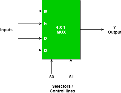
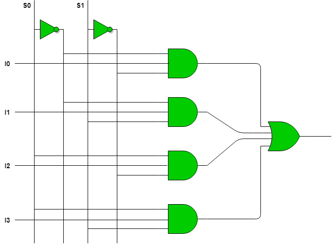
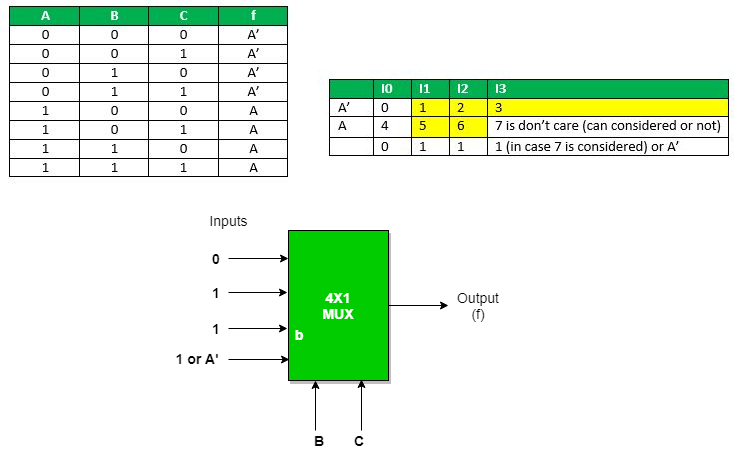
Multiplexer can act as universal combinational circuit. All the standard logic gates can be implemented with multiplexers.
a) Implementation of NOT gate using 2 : 1 Mux
NOT Gate :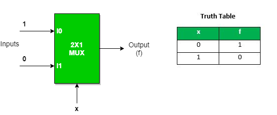
We can analyze it
Y = x’.1 + x.0 = x’
It is NOT Gate using 2:1 MUX.
The implementation of NOT gate is done using “n” selection lines. It cannot be implemented using “n-1” selection lines. Only NOT gate cannot be implemented using “n-1” selection lines.
b) Implementation of AND gate using 2 : 1 Mux
AND GATE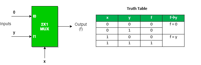
This implementation is done using “n-1” selection lines.
c) Implementation of OR gate using 2 : 1 Mux using “n-1” selection lines.
OR GATE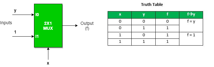
Implementation of NAND, NOR, XOR and XNOR gates requires two 2:1 Mux. First multiplexer will act as NOT gate which will provide complemented input to the second multiplexer.
d) Implementation of NAND gate using 2 : 1 Mux
NAND GATE
e) Implementation of NOR gate using 2 : 1 Mux
NOR GATE
f) Implementation of EX-OR gate using 2 : 1 Mux
EX-OR GATE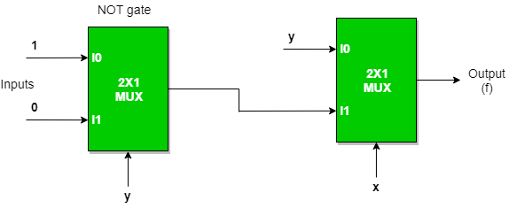
g) Implementation of EX-NOR gate using 2 : 1 Mux
EX-NOR GATE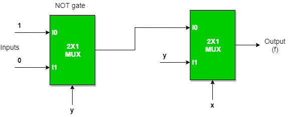
Implementation of Higher order MUX using lower order MUX
a) 4 : 1 MUX using 2 : 1 MUX
Three(3) 2 : 1 MUX are required to implement 4 : 1 MUX.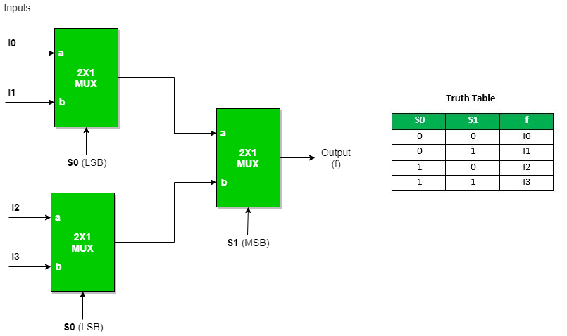
Similarly,
While 8 : 1 MUX require seven(7) 2 : 1 MUX, 16 : 1 MUX require fifteen(15) 2 :1 MUX, 64 : 1 MUX requires sixty three(63) 2 : 1 MUX.
Hence, we can draw a conclusion,
2n : 1 MUX requires (2n- 1) 2 : 1 MUX.
b) 16 : 1 MUX using 4 : 1 MUX
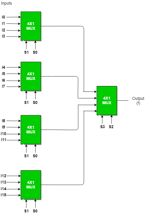
In general, to implement B : 1 MUX using A : 1 MUX , one formula is used to implement the same.
B / A = K1,
K1/ A = K2,
K2/ A = K3
………………
KN-1 / A = KN = 1 (till we obtain 1 count of MUX).
And then add all the numbers of MUXes = K1 + K2 + K3 + …. + KN.
For example : To implement 64 : 1 MUX using 4 : 1 MUX
Using the above formula, we can obtain the same.
64 / 4 = 16
16 / 4 = 4
4 / 4 = 1 (till we obtain 1 count of MUX)
Hence, total number of 4 : 1 MUX are required to implement 64 : 1 MUX = 16 + 4 + 1 = 21.
An example to implement a boolean function if minimal and don’t care terms are given using MUX.
f ( A, B, C) = Σ ( 1, 2, 3, 5, 6 ) with don’t care (7) using 4 : 1 MUX using as
a) AB as select : Expanding the minterms to its boolean form and will see its 0 or 1 value in Cth place so that they can be placed in that manner.
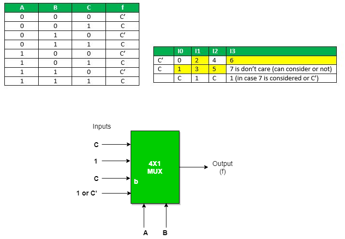
b) AC as select : Expanding the minterms to its boolean form and will see its 0 or 1 value in Bth place so that they can be place in that manner.
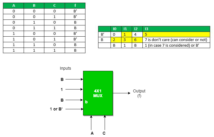
c) BC as select : Expanding the minterms to its boolean form and will see its 0 or 1 value in Ath place so that they can be place in that manner.
Where Do I Start to Electronics?
All sorted into a series of categories: concepts, technologies, skills, hook-up guides, and projects.
make the world of electronics as approachable as possible
In a job and our ability it takes the concept of thinking from ASK? (Attitude --- Skill --- Knowledge) and the willingness to continue to add capabilities so that we are able to develop electronics to be more capable, the process is a little explained
Concept
The concept cover the really low-level, nitty-gritty areas of electronics. This is We must to be learn in an electronics classroom .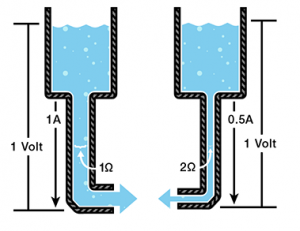
Technology
Technology speak specifically about the components, standards, and technologies which make all of this possible. You can learn how GPS works and how you might add it to your project. Or you can read all about resistors, diodes, and other basic electronics components.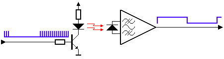
Skills
Electronics isn’t just about calculating currents, voltages, and resistances. We have to learn some (sweet) skills to build ! to start in the skills :
Hook-Ups
Are you looking for a quick primer on using a new Arduino shield or breakout board?: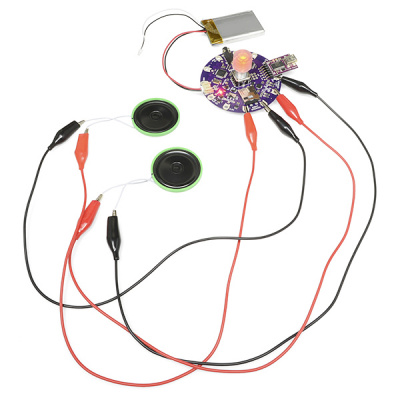


Fastest Finger First Indicator
Quiz-type game shows are increasingly becoming popular on television these days. In such games, fastest finger first indicators (FFFIs) are used to test the player’s reaction time. The player’s designated number is displayed with an audio alarm when the player presses his entry button.

The circuit presented here determines as
to which of the four contestants first pressed the button and locks out
the remaining three entries. Simultaneously, an audio alarm and the
correct decimal number display of the corresponding contestant are
activated.
When a contestant presses his switch,
the corresponding output of latch IC2 (7475) changes its logic state
from 1 to 0. The combinational circuitry comprising dual 4-input NAND
gates of IC3 (7420) locks out subsequent entries by producing the
appropriate latch-disable signal.
Advertisement
Priority
encoder IC4 (74147) encodes the active-low input condition into the
corresponding binary coded decimal (BCD) number output. The outputs of
IC4 after inversion by inverter gates inside hex inverter 74LS04 (IC5)
are coupled to BCDto- 7-segment decoder/display driver IC6 (7447). The
output of IC6 drives common anode 7-segment LED display (DIS.1, FND507
or LT542).
The audio alarm generator comprises
clock oscillator IC7 (555), whose output drives a loudspeaker. The
oscillator frequency can be varied with the help of preset VR1. Logic 0
state at one of the outputs of IC2 produces logic 1 input condition at
pin 4 of IC7, there by enabling the audio oscillator.
IC7 needs +12V DC supply for sufficient
alarm level. The remaining circuit operates on regulated +5V DC supply,
which is obtained using IC1 (7805).
Once the organiser identifies the
contestant who pressed the switch first, he disables the audio alarm and
at the same time forces the digital display to ‘0’ by pressing reset
push button S5.
With a slight modification, this circuit can accommodate more than four contestants.
Remote Operated Spy Robot Circuit
To design a robot which can capture audio and video information from the surroundings and can be sent to the remote area? This article explains you how design a spy robot which can be controlled by the remote. The maximum controllable range is 125 meters. The remote has four switches to control the robot in four directions.
The robot senses the surroundings through
the CCD camera and sends to the receiver through the Radio Frequency
wireless communication.
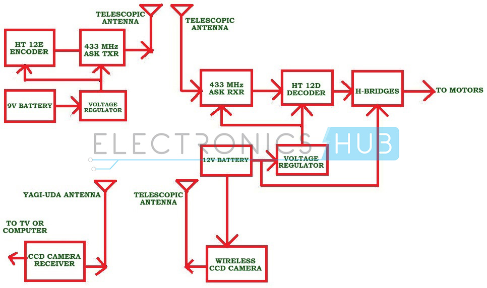
- HT12E encoder
- HT12D decoder
- RF 433 MHz Transmitter and Receiver
- L293D motor driver
- Wireless CCD camera
- push buttons – 4
- DC battery – 12V, 1.3 Ah
- 9V DC battery
- Robot
- Resistors – 33k,750k
- SPST switch – 1
- NOT gates – 4
Remote Operated Spy Robot Circuit Diagram and Design:
Remote operated spy robot has mainly two sections, one is remote control section used to control the robot and other one is video transmission section used to transmit audio and video information.Remote Control Section:
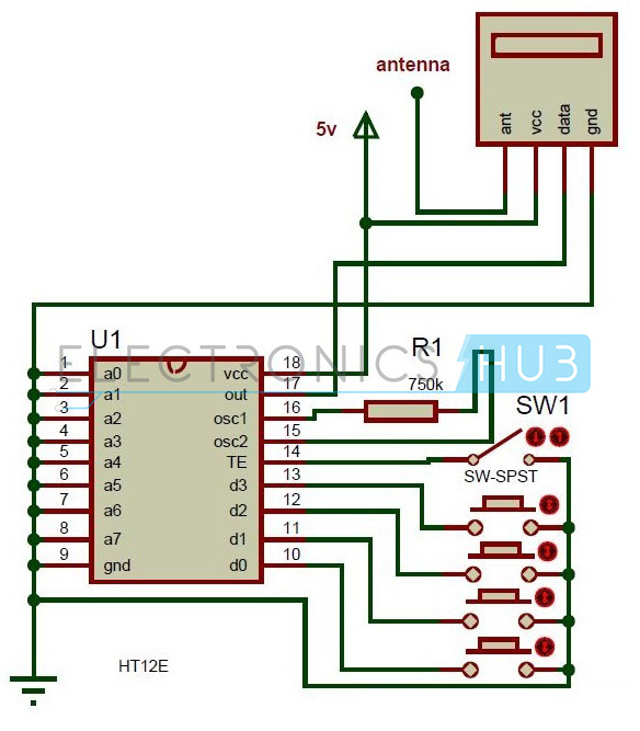
Remote Section of Spy Robot Circuit
Video Transmission Section:
In this section, major components are wireless camera, RF receiver and Robot.Wireless CCD Camera: The operating voltage of CCD camera is 12V DC. The supply for this camera is taken from the motors battery. The output signals of this camera are in the form of audio and video. These types of cameras are commonly available in the market.

Remote Operated Spy Robot Circuit – Video Transmission Section
RF Receiver:
ASK receiver receives the serial data transmitted by the transmitter and gives it decoder to convert it to the parallel. This parallel data is given to the L293D motor driver IC to control the robot motors. Here LED D5 indicates the valid transmission.L293D Motor Driver:
L293d is a Dual H-bridge motor driver. Used as a current amplifier since it takes low current control signal and provides higher current signal as output. This output signal is used to drive the motors.This IC drives 2 motors simultaneously, both in forward direction and reverse direction. Motor 1 direction can be controlled based on logic inputs at IN1 and IN2. Motor 2 operations are controlled based on the inputs at IN3 and IN4. Here the motors are operated with the voltage applied at pin 8.
- IN1=0 and IN2=0 -> Motor 1 idle
- IN1=0 and IN2=1 -> Motor 1 Anti-clock wise direction
- IN1=1 and IN2=0 -> Motor 1 Clock wise direction
- IN1=1 and IN2=1 -> Motor 1 idle
- IN3=0 and IN4=0 -> Motor 2 idle
- IN3=0 and IN4=1 -> Motor 2 Anti-clock wise direction
- IN3=1 and IN4=0 -> Motor 2 Clock wise direction
- IN3=1 and IN4=1 -> Motor 2 idle
How to Operate Remote Operated Spy Robot:
- Give the connections as per the circuit diagram.
- Arrange the wireless CCD camera to the robot.
- Give the wireless camera receiver connection to the computer or TV.
- Now switch on the both robot and remote supplies.
- Control the spy robot using remote. Now you can observe the robot surroundings in your computer or TV.
Remote Operated Spy Robot Project Output Video:
Remote Operated Spy Robot Applications:
- This spy robot is used to observe the behavior of wild animals where human beings cannot reach.
- Used in army applications to detect the bombs.
- Used in industries.
Remote Operated Spy Robot Limitations:
- This system does not work for longer distances.
- This is a theoretical circuit and may require some changes to implement practically.
Maintaining a desired system performance despite disturbance
Simple Combination Lock
- 4001 quad NOR gate (Radio Shack catalog # 276-2401)
- 4070 quad XOR gate (Radio Shack catalog # 900-6906)
- Two, eight-position DIP switches (Radio Shack catalog # 275-1301)
- Two light-emitting diodes (Radio Shack catalog # 276-026 or equivalent)
- Four 1N914 “switching” diodes (Radio Shack catalog # 276-1122)
- Ten 10 kΩ resistors
- Two 470 Ω resistors
- Pushbutton switch, normally open (Radio Shack catalog # 275-1556)
- Two 6 volt batteries
This experiment may be built using only one 8-position DIP switch, but the concept is easier to understand if two switch assemblies are used. The idea is, one switch acts to hold the correct code for unlocking the lock, while the other switch serves as a data entry point for the person trying to open the lock. In real life, of course, the switch assembly with the “key” code set on it must be hidden from the sight of the person opening the lock, which means it must be physically located elsewhere from where the data entry switch assembly is. This requires two switch assemblies. However, if you understand this concept clearly, you may build a working circuit with only one 8-position switch, using the left four switches for data entry and the right four switches to hold the “key” code.
For extra effect, choose different colors of LED: green for “Go” and red for “No go.”
LEARNING OBJECTIVES
- Using XOR gates as bit comparators
- How to build simple gate functions with diodes and a pull-up/down resistor
- Using NOR gates as controlled inverters
SCHEMATIC DIAGRAM
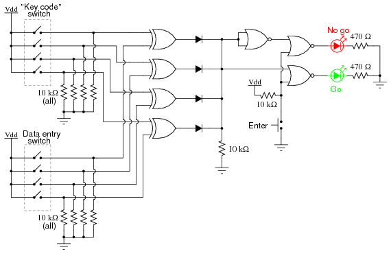
ILLUSTRATION
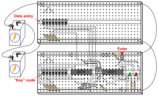
INSTRUCTIONS
This circuit illustrates the use of XOR (Exclusive-OR) gates as bit comparators. Four of these XOR gates compare the respective bits of two 4-bit binary numbers, each number “entered” into the circuit via a set of switches. If the two numbers match, bit for bit, the green “Go” LED will light up when the “Enter” pushbutton switch is pressed. If the two numbers do not exactly match, the red “No go” LED will light up when the “Enter” pushbutton is pressed.
Because four bits provides a mere sixteen possible combinations, this lock circuit is not very sophisticated. If it were used in a real application such as a home security system, the “No go” output would have to be connected to some kind of siren or other alarming device so that the entry of an incorrect code would deter an unauthorized person from attempting another code entry. Otherwise, it would not take much time to try all combinations (0000 through 1111) until the correct one was found! In this experiment, I do not describe how to work this circuit into a real security system or lock mechanism, but only how to make it recognize a pre-entered code.
The “key” code that must be matched at the data entry switch array should be hidden from view, of course. If this were part of a real security system, the data entry switch assembly would be located outside the door and the key code switch assembly behind the door with the rest of the circuitry. In this experiment, you will likely locate the two switch assemblies on two different breadboards, but it is entirely possible to build the circuit using just a single (8-position) DIP switch assembly. Again, the purpose of the experiment is not to make a real security system, but merely to introduce you to the principle of XOR gate code comparison.
It is the nature of an XOR gate to output a “high” (1) signal if the input signals are not the same logic state. The four XOR gates’ output terminals are connected through a diode network which functions as a four-input OR gate: if any of the four XOR gates outputs a “high” signal—indicating that the entered code and the key code are not identical—then a “high” signal will be passed on to the NOR gate logic. If the two 4-bit codes are identical, then none of the XOR gate outputs will be “high,” and the pull-down resistor connected to the common sides of the diodes will provide a “low” signal state to the NOR logic.
The NOR gate logic performs a simple task: prevent either of the LEDs from turning on if the “Enter” pushbutton is not pressed. Only when this pushbutton is pressed can either of the LEDs energize. If the Enter switch is pressed and the XOR outputs are all “low,” the “Go” LED will light up, indicating that the correct code has been entered. If the Enter switch is pressed and any of the XOR outputs are “high,” the “No go” LED will light up, indicating that an incorrect code has been entered. Again, if this were a real security system, it would be wise to have the “No go” output do something that deters an unauthorized person from discovering the correct code by trial-and-error. In other words, there should be some sort of penalty for entering an incorrect code.


Tidak ada komentar:
Posting Komentar