
In the 21 first Century is electronic devices are changing the way humans interact with electronics machines for example: laptops, smartphones, internet, ROBOT, TV, video, organs, radio, electronic cars, and electronic instrumentation control equipment for aircraft and submarines as well as sophisticated weaponry weapons; so that a proposal is discussed how the equipment works so that it can be faster and more reliable and attractive to the environment in which electronic equipment works; one form of electronic circuits to improve the capabilities of electronic equipment is by displaying the description and the reality inside the electron bridge circuit passing through or setting up a complete and controlled electronic circuit .
e- Bridge in the field of electronic engineering and the more modern one is the international electronic communication network, namely INTERNET, so the bridge is defined as how an electron movement from a system is connected to other electron systems and integrated closed and open or better known as networking. in the field of electronics a series of application and interpretation of a bridge is to process the movement of electrons to be more flexible and safer in durability so that the appearance of actuators such as motors - LED lights as well as LED monitors and other electronic panel panel displays become more attractive and flexible also has memory and controlled data input speed; then many of us know in electronics various types of bridge circuits which function to control - setting and processing input data towards an accurate output display which may even be strengthened in the sense (e-DIREW [e-Data - Input - Read - Write] become e-REWIND [e-Read - Write - IN - Display] in electronic engineering the display can be in the form of stepper motors, DC, AC, Servo or Dynamo; The display can also be in the form of indicator lights such as LEDs (LED monitors), Speakers, Touch screens, DVD player printers and so on. Subsequent developments of electronic science were developed continuously by the United States government in the form of communication electronics, namely the creation of computer computers for large databases and memory as well as fast data access speeds - precisely and accurately, in the development of this electronic machine which is a combination from a series of electronic circuit components into integrated electronic circuits that are continuously integrated and developed to communicate all electronic equipment equipment to communicate with each other both individually, in groups, in groups and globally. Electronic technology that combines all equipment for electronic machine tools such as computers - laptops and smartphones as well as television and radio is possible by building larger bridges, namely INTERNET; where the bridge on the INTERNET is known as NETWORKING. in NETWORKING INTERNET there are so many concepts and forms of Bridge that of course every country uses a different Bridge concept in accordance with the ability to accept electronic technology and its ability to accommodate energy resources in the concept of capacity availability of electronic communication both electronic component resources - power source equipment for electronic machinery --- satellite capability resources as well as optical communication - and form contour areas of a country so that the flexibility of the electronic communication movement is in perfect efficiency. for this reason I will discuss here and I describe the e-Bridge Electronics condition that exists on earth for the present time, namely in the 21st century, which of course we as electronics experts always put forward the concept for the development of e-Bridge network, especially in my previous discussion Regarding the concept of 7 stages of electronic development, namely the 6th stage where the development of cables and wireless cables and materials for electron paths are better and more perfect so that the development of communication electronics can penetrate the 22nd century where stages 1 through stage 7 have been discussed in my previous book, it became more modern and the quality of reliable electronic technology and appearance.
LOVE = Line On Victory Endless
( ON / OFF Gen. Mac Tech __ e- Bridge )
Computation Structures

Digital systems are at the heart of the information age in which we live, allowing us to store, communicate and manipulate information quickly and reliably. This computer science course is a bottom-up exploration of the abstractions, principles, and techniques used in the design of digital and computer systems. If you have a rudimentary knowledge of electricity and some exposure to programming, roll up your sleeves, join in and design a computer system! We must to combine electronic interfaces between the physical world and digital devices . in the 21st century, one of the applications is the internet inside The Internet of Things (IoT) is expanding at a rapid rate, and it is becoming increasingly important for professionals to understand what it is, how it works, and how to harness its power to improve your business. We want to explore electronic circuit on analog and digital have to interact with the IoT bridge between the cyber- and physical worlds, in order to create efficiencies or solve business problems. We will look at IoT sensors, actuators and intermediary devices that connect things to the internet, as well as electronics and systems, both of which underpin how the Internet of Things works and what it is designed to do.

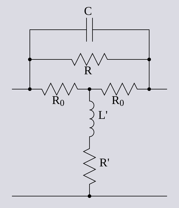
The concept of electronic bridges is as shown above
Lets"go to introduction electronic Bridge : Bridge in electronic means Complete electronic metering or Control Instrumentation electronic for reliable and appearance at electronic device performance .
XO___XO Different Types of Bridge Circuits and Circuit Diagrams
A bridge circuit is one kind of electrical circuit
wherein the two branches of the circuit are linked to a third branch
–which is connected in between the first two branches at some middle
point along them. The bridge circuit was mainly designed for measurement
purpose in the laboratory. And, one of the middle linking points is
adjusted when it is used for a specific purpose. These circuits are used
in linear, nonlinear, power conversion, instrumentation, filtering,
etc.
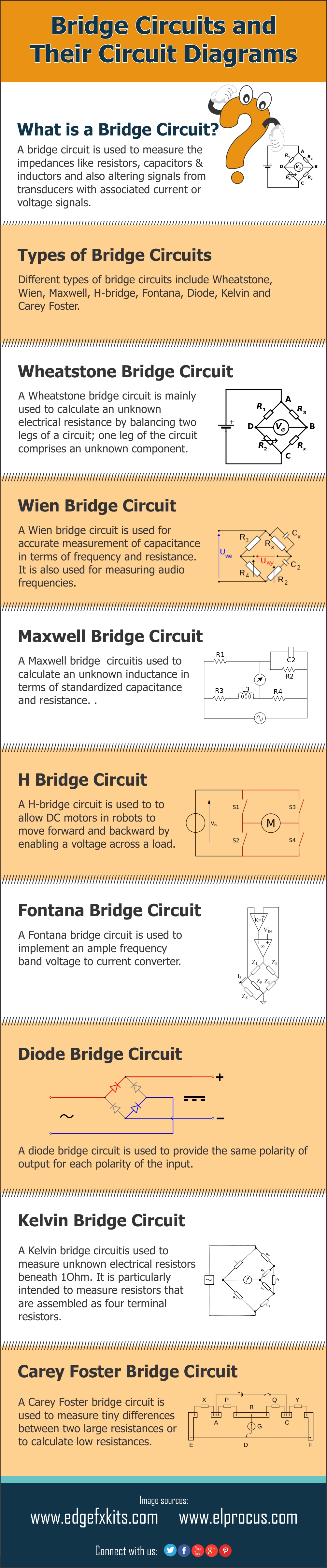
The best known bridge circuit is the Wheatstone bridge;
the term was invented by “Samuel Hunter Christie” and popularized by
“Charles Wheatstone”. A bridge circuit is mainly used to measure
resistance. This circuit is built with four resistors: R1, R2, R3 and
RX; wherein the two resistors are with known values R1 & R3, one
resistor’s resistance is to be concluded Rx, and one which is changeable
and adjusted R2. Two opposite vertices are associated with a supply of
electric current like a battery, and a galvanometer is connected across the additional two vertices. The variable resistor is familiarized until the galvanometer reads zero.
It is known that the relation between the variable resistor and its
neighbor resistor R1 is equivalent to the relation between the unknown
resistor and its neighbor R3, which permits the unknown value of the
resistor to be calculated. The Wheatstone bridge circuit has also been
widespread to calculate impedance in AC circuits, and also to calculate
inductance, resistance, capacitance, and dissipation factor
individually.
Different arrangements are identified as Wien bridge,
Heaviside and Maxwell bridge. All the circuits are based on a similar
concept, which is to contrast the o/p of two potentiometers sharing a
frequent source.
Wheatstone bridge and Its Working
The term “Wheatstone bridge” is also
called as Resistance Bridge that is, invented by “Charles Wheatstone”.
This bridge circuit is used to calculate the unknown resistance values
and as a means of regulating measuring instrument, ammeters, voltmeters,
etc. But, the present digital millimeters offer the easiest way to
calculate a resistance. In recent days, Wheatstone bridge is used in
many applications such as; it can be used with modern op-amps to
interface various sensors and transducers to amplifier circuits.
This bridge circuit is constructed with two simple serial and parallel
resistances in between a voltage supply terminal and ground terminals.
When the bridge is balanced, then the ground terminal produces a zero
voltage difference between the two parallel branches. A Wheatstone
bridge consists of two i/p and two o/p terminals includes of four
resistors arranged in a diamond shape.
Wheatstone Bridge and Its Working
A Wheatstone bridge is widely used to measure the electrical resistance. This circuit is built with two known resistors,
one unknown resistor and one variable resistor connected in the form of
bridge. When the variable resistor is adjusted, then the current in the
galvanometer becomes zero, the ratio of two two unknown resistors is
equal to the ratio of value of unknown resistance and adjusted value of
variable resistance. By using a Wheatstone Bridge the unknown
electrical resistance value can easily measure.
Wheatstone Bridge Circuit Arrangement
The circuit arrangement of the
Wheatstone bridge is shown below. This circuit is designed with four
arms, namely AB, BC, CD & AD and consists of electrical resistance
P, Q, R and S. Among these four resistances, P and Q are known fixed
electrical resistances. A galvanometer is connected between the B & D
terminals via an S1 switch. The voltage source is connected to the A
&C terminals via a switch S2. A variable resistor ‘S’ is connected
between the terminals C & D. The potential at terminal D varies when
the value of the variable resistor adjusts. For instance, currents I1
and I2 are flowing through the points ADC and ABC. When the resistance
value of arm CD varies, then the I2 current will also vary.
If we tend to adjust the variable
resistance one state of affairs could return once when the voltage drop
across the resistor S that is I2.S becomes specifically capable to the
voltage drop across resistor Q i.e I1.Q. Thus the potential of the point
B becomes equal to the potential of the point D hence the potential
difference b/n these two points is zero hence current through
galvanometer is zero. Then the deflection in the galvanometer is zero
when the S2 switch is closed.
Wheatstone Bridge Derivation
From the above circuit, currents I1 and I2 are
I1=V/P+Q and I2=V/R+SNow potential of point B with respect to point C is the voltage drop across the Q transistor, then the equation is
Potential of point D with respect to C is the voltage drop across the resistor S, then the equation is
I2S=VS/R+S …………………………..(2)
From the above equation 1 and 2 we get,
VQ/P+Q = VS/R+S
` Q/P+Q = S/R+S
P+Q/Q=R+S/S
P/Q+1=R/S+1
R=SxP/Q
Here in the above equation, the value of P/Q and S are known, so R value can easily be determined.
The electrical resistances of Wheatstone
bridge such as P and Q are made of definite ratio, they are 1:1; 10:1
(or) 100:1 known as ratio arms and the rheostat arm S is made always
variable from 1-1,000 ohms or from 1-10,000 ohms
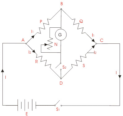
Example of Wheatstone Bridge
The following circuit is an unbalanced
Wheatstone bridge, calculate the o/p voltage across C and D points and
the value of the resistor R4 is required to balance the bridge circuit.
Vc= (R2/(R1+R2)) X Vs
R2=120ohms, R1=80 ohms, Vs=100
Substitute these values in the above equation
Vc= (120/(80+120)) X 100
= 60 volts
The second series arm in the above circuit is ADB
VD = R4/(R3+R4) X Vs
VD= 160/ (480+160) X 100
=25 Volts
The voltage across points C & D is given as
Vout= VC-VD
Vout= 60-25 = 35 volts.
The value of R4 resistor is required to balance the Wheatstone bridge bridge is given as:
R4= R2 R3/R1
120X480/ 80
720 ohms.
=25 Volts
The voltage across points C & D is given as
Vout= VC-VD
Vout= 60-25 = 35 volts.
The value of R4 resistor is required to balance the Wheatstone bridge bridge is given as:
R4= R2 R3/R1
120X480/ 80
720 ohms.
So, finally we can conclude that, the
Wheatstone bridge has two i/p & two o/p terminals namely A & B,
C& D. When the above circuit is balanced, the voltage across the o/p
terminals is zero volts. When the Wheatstone bridge is unbalanced, the
o/p voltage may be either +ve or –ve depending upon the unbalance
direction.
Application of Wheatstone Bridge
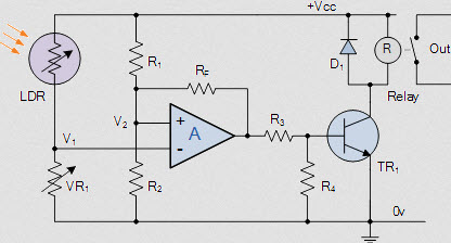
The application of Wheatstone bridge is light detector using Wheatstone bridge circuit
Balanced bridge circuits are used in many electronic applications
to measure changes in intensity of light, strain or pressure. The
different types of resistive sensors which can be used in a Wheatstone
bridge circuit include: potentiometers, LDR’s, strain gauges and
thermistor’s, etc.
Wheatstone bridge applications are used
to sense electrical and mechanical quantities. But, the simple
Wheatstone bridge application is light measurement using photoresistive
device. In the Wheatstone bridge circuit, a light dependent resistor is
placed in the place of one of the resistors.
An LDR is a passive resistive sensor,
that is used to convert the visible light levels into a change in
resistance and later a voltage. LDR can be used to measure and monitor
the light intensity level. LDR has a several Megha ohms resistance in
dim or dark light around 900Ω at a 100 Lux of a light intensity and down
to around 30ohms in a bright light. By connecting the light dependent
resistor in the Wheatstone bridge circuit, we can measure and monitor
the changes in the light levels.
The Wheatstone Bridge


I = V ÷ R = 12V ÷ (10Ω + 20Ω) = 0.4A
The voltage at point C, which is also the voltage drop across the lower resistor, R2 is calculated as:
VR2 = I × R2 = 0.4A × 20Ω = 8 volts
Then we can see that the source voltage VS is divided among the two series resistors in direct proportion to their resistances as VR1 = 4V and VR2 = 8V.
This is the principle of voltage division, producing what is commonly
called a potential divider circuit or voltage divider network.Now if we add another series resistor circuit using the same resistor values in parallel with the first we would have the following circuit.

But something else equally as important is that the voltage difference between point C and point D will be zero volts as both points are at the same value of 8 volts as: C = D = 8 volts, then the voltage difference is: 0 volts
When this happens, both sides of the parallel bridge network are said to be balanced because the voltage at point C is the same value as the voltage at point D with their difference being zero.
Now let’s consider what would happen if we reversed the position of the two resistors, R3 and R4 in the second parallel branch with respect to R1 and R2.

VR4 = 0.4A × 10Ω = 4 volts
Now with VR4 having 4 volts dropped across it, the voltage difference between points C and D will be 4 volts as: C = 8 volts and D = 4 volts. Then the difference this time is: 8 – 4 = 4 voltsThe result of swapping the two resistors is that both sides or “arms” of the parallel network are different as they produce different voltage drops. When this happens the parallel network is said to be unbalanced as the voltage at point C is at a different value to the voltage at point D.
Then we can see that the resistance ratio of these two parallel arms, ACB and ADB, results in a voltage difference between 0 volts (balanced) and the maximum supply voltage (unbalanced), and this is the basic principal of the Wheatstone Bridge Circuit.
So we can see that a Wheatstone bridge circuit can be used to compare an unknown resistance RX with others of a known value, for example, R1 and R2, have fixed values, and R3 could be variable. If we connected a voltmeter, ammeter or classically a galvanometer between points C and D, and then varied resistor, R3 until the meters read zero, would result in the two arms being balanced and the value of RX, (substituting R4) known as shown.
Wheatstone Bridge Circuit


Wheatstone Bridge Example No1
The following unbalanced Wheatstone Bridge is constructed. Calculate the output voltage across points C and D and the value of resistor R4 required to balance the bridge circuit.
For the first series arm, ACB

For the second series arm, ADB

The voltage across points C-D is given as:


Wheatstone Bridge Light Detector
Balanced bridge circuits find many useful electronics applications such as being used to measure changes in light intensity, pressure or strain. The types of resistive sensors that can be used within a wheatstone bridge circuit include: photoresistive sensors (LDR’s), positional sensors (potentiometers), piezoresistive sensors (strain gauges) and temperature sensors (thermistor’s), etc.There are many wheatstone bridge applications for sensing a whole range of mechanical and electrical quantities, but one very simple wheatstone bridge application is in the measurement of light by using a photoresistive device. One of the resistors within the bridge network is replaced by a light dependent resistor, or LDR.
An LDR, also known as a cadmium-sulphide (Cds) photocell, is a passive resistive sensor which converts changes in visible light levels into a change in resistance and hence a voltage. Light dependent resistors can be used for monitoring and measuring the level of light intensity, or whether a light source is ON or OFF.
A typical Cadmium Sulphide (CdS) cell such as the ORP12 light dependent resistor typically has a resistance of about one Megaohm (MΩ) in dark or dim light, about 900Ω at a light intensity of 100 Lux (typical of a well lit room), down to about 30Ω in bright sunlight. Then as the light intensity increases the resistance reduces. By connecting a light dependant resistor to the Wheatstone bridge circuit above, we can monitor and measure any changes in the light levels as shown.
Wheatstone Bridge Light Detector

The op-amp is connected as a voltage comparator with the reference voltage VD applied to the non-inverting pin. In this example, as both R3 and R4 are of the same 10kΩ value, the reference voltage set at point D will therefore be equal to half of Vcc. That is Vcc/2.
The potentiometer, VR1 sets the trip point voltage VC, applied to the inverting input and is set to the required nominal light level. The relay turns “ON” when the voltage at point C is less than the voltage at point D.
Adjusting VR1 sets the voltage at point C to balance the bridge circuit at the required light level or intensity. The LDR can be any cadmium sulphide device that has a high impedance at low light levels and a low impedance at high light levels.
Note that the circuit can be used to act as a “light-activated” switching circuit or a “dark-activated” switching circuit simply by transposing the LDR and R3 positions within the design.
The Wheatstone Bridge has many uses in electronic circuits other than comparing an unknown resistance with a known resistance. When used with Operational Amplifiers, the Wheatstone bridge circuit can be used to measure and amplify small changes in resistance, RX due, for example, to changes in light intensity as we have seen above.
But the bridge circuit is also suitable for measuring the resistance change of other changing quantities, so by replacing the above photo-resistive LDR light sensor for a thermistor, pressure sensor, strain gauge, and other such transducers, as well as swapping the positions of the LDR and VR1, we can use them in a variety of other Wheatstone bridge applications.
Also more than one resistive sensor can be used within the four arms (or branches) of the bridge formed by the resistors R1 to R4 to produce “full-bridge”, “half-bridge” or “quarter-bridge circuit arrangements providing thermal compensation or automatic balancing of the Wheatstone bridge.
The Wien Bridge Oscillator
The Wien Bridge Oscillator uses uses two RC networks connected together to produce a sinusoidal oscillator .In the RC Oscillator tutorial we saw that a number of resistors and capacitors can be connected together with an inverting amplifier to produce an oscillating circuit.
One of the simplest sine wave oscillators which uses a RC network in place of the conventional LC tuned tank circuit to produce a sinusoidal output waveform, is called a Wien Bridge Oscillator.
The Wien Bridge Oscillator is so called because the circuit is based on a frequency-selective form of the Wheatstone bridge circuit. The Wien Bridge oscillator is a two-stage RC coupled amplifier circuit that has good stability at its resonant frequency, low distortion and is very easy to tune making it a popular circuit as an audio frequency oscillator but the phase shift of the output signal is considerably different from the previous phase shift RC Oscillator.
The Wien Bridge Oscillator uses a feedback circuit consisting of a series RC circuit connected with a parallel RC of the same component values producing a phase delay or phase advance circuit depending upon the frequency. At the resonant frequency ƒr the phase shift is 0o. Consider the circuit below.
RC Phase Shift Network

At low frequencies the reactance of the series capacitor (C1) is very high so acts a bit like an open circuit, blocking any input signal at Vin resulting in virtually no output signal, Vout. Likewise, at high frequencies, the reactance of the parallel capacitor, (C2) becomes very low, so this parallel connected capacitor acts a bit like a short circuit across the output, so again there is no output signal.
So there must be a frequency point between these two extremes of C1 being open-circuited and C2 being short-circuited where the output voltage, VOUT reaches its maximum value. The frequency value of the input waveform at which this happens is called the oscillators Resonant Frequency, (ƒr).
At this resonant frequency, the circuits reactance equals its resistance, that is: Xc = R, and the phase difference between the input and output equals zero degrees. The magnitude of the output voltage is therefore at its maximum and is equal to one third (1/3) of the input voltage as shown.
Oscillator Output Gain and Phase Shift

Wien Bridge Oscillator Frequency

- Where:
- ƒr is the Resonant Frequency in Hertz
- R is the Resistance in Ohms
- C is the Capacitance in Farads
We know from our AC Theory tutorials that the real part of the complex impedance is the resistance, R while the imaginary part is the reactance, X. As we are dealing with capacitors here, the reactance part will be capacitive reactance, Xc.
The RC Network

Therefore the total DC impedance of the series combination (R1C1) we can call, ZS and the total impedance of the parallel combination (R2C2) we can call, ZP. As ZS and ZP are effectively connected together in series across the input, VIN, they form a voltage divider network with the output taken from across ZP as shown.
Lets assume then that the component values of R1 and R2 are the same at: 12kΩ, capacitors C1 and C2 are the same at: 3.9nF and the supply frequency, ƒ is 3.4kHz.
Series Circuit
The total impedance of the series combination with resistor, R1 and capacitor, C1 is simply:
For the lower parallel impedance ZP, as the two components are in parallel, we have to treat this differently because the impedance of the parallel circuit is influenced by this parallel combination.
Parallel Circuit
The total impedance of the lower parallel combination with resistor, R2 and capacitor, C2 is given as:


If we now place this RC network across a non-inverting amplifier which has a gain of 1+R1/R2 the following basic Wien bridge oscillator circuit is produced.
Wien Bridge Oscillator

The other part, which forms the series and parallel combinations of R and C forms the feedback network and are fed back to the non-inverting input terminal (positive or regenerative feedback) via the RC Wien Bridge network and it is this positive feedback combination that gives rise to the oscillation.
The RC network is connected in the positive feedback path of the amplifier and has zero phase shift a just one frequency. Then at the selected resonant frequency, ( ƒr ) the voltages applied to the inverting and non-inverting inputs will be equal and “in-phase” so the positive feedback will cancel out the negative feedback signal causing the circuit to oscillate.
The voltage gain of the amplifier circuit MUST be equal too or greater than three “Gain = 3” for oscillations to start because as we have seen above, the input is 1/3 of the output. This value, ( Av ≥ 3 ) is set by the feedback resistor network, R1 and R2 and for a non-inverting amplifier this is given as the ratio 1+(R1/R2).
Also, due to the open-loop gain limitations of operational amplifiers, frequencies above 1MHz are unachievable without the use of special high frequency op-amps.
Wien Bridge Oscillator Example No1
Determine the maximum and minimum frequency of oscillations of a Wien Bridge Oscillator circuit having a resistor of 10kΩ and a variable capacitor of 1nF to 1000nF.The frequency of oscillations for a Wien Bridge Oscillator is given as:
Wien Bridge Oscillator Lowest Frequency

Wien Bridge Oscillator Highest Frequency

Wien Bridge Oscillator Example No2
A Wien Bridge Oscillator circuit is required to generate a sinusoidal waveform of 5,200 Hertz (5.2kHz). Calculate the values of the frequency determining resistors R1 and R2 and the two capacitors C1 and C2 to produce the required frequency.Also, if the oscillator circuit is based around a non-inverting operational amplifier configuration, determine the minimum values for the gain resistors to produce the required oscillations. Finally draw the resulting oscillator circuit.


Wien Bridge Oscillator Circuit Example No2

Wien Bridge Oscillator Summary
Then for oscillations to occur in a Wien Bridge Oscillator circuit the following conditions must apply.- With no input signal a Wien Bridge Oscillator produces continuous output oscillations.
- The Wien Bridge Oscillator can produce a large range of frequencies.
- The Voltage gain of the amplifier must be greater than 3.
- The RC network can be used with a non-inverting amplifier.
- The input resistance of the amplifier must be high compared to R so that the RC network is not overloaded and alter the required conditions.
- The output resistance of the amplifier must be low so that the effect of external loading is minimized.
- Some method of stabilizing the amplitude of the oscillations must be provided. If the voltage gain of the amplifier is too small the desired oscillation will decay and stop. If it is too large the output will saturate to the value of the supply rails and distort.
- With amplitude stabilisation in the form of feedback diodes, oscillations from the Wien Bridge oscillator can continue indefinitely.
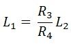
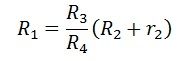
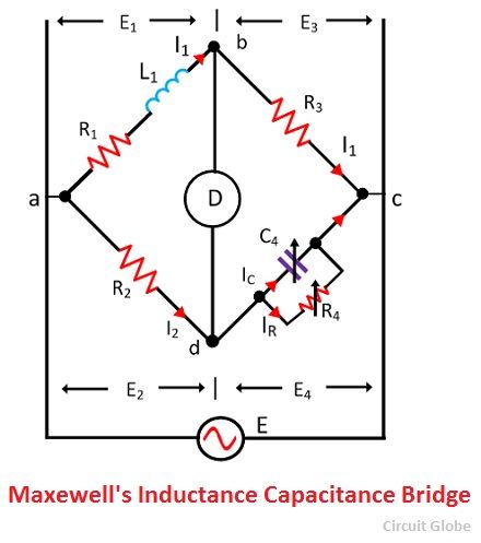
Maxwell’s Bridge
Definition: The bridge used for the measurement of self-inductance of the circuit is known as the Maxwell bridge. It is the advanced form of the Wheatstone bridge. The Maxwell bridge works on the principle of the comparison, i.e., the value of unknown inductance is determined by comparing it with the known value or standard value.
Types of Maxwell’s Bridge
Two methods are used for determining the self-inductance of the circuit. They are- Maxwell’s Inductance Bridge
- Maxwell’s inductance Capacitance Bridge
Maxwell’s Inductance Bridge
In such type of bridges, the value of unknown resistance is determined by comparing it with the known value of the standard self-inductance. The connection diagram for the balance Maxwell bridge is shown in the figure below.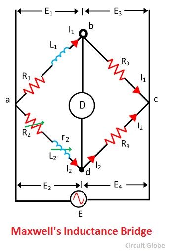
Let, L1 – unknown inductance of resistance R1.
L2 – Variable inductance of fixed resistance r1.
R2 – variable resistance connected in series with inductor L2.
R3, R4 – known non-inductance resistance
At balance,
The value of the R3 and the R4 resistance varies from 10 to 1000 ohms with the help of the resistance box. Sometimes for balancing the bridge, the additional resistance is also inserted into the circuit.
The phasor diagram of Maxwell’s inductance bridge is shown in the figure below.
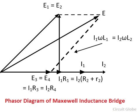
Let, L1 – unknown inductance of resistance R1.
R1 – Variable inductance of fixed resistance r1.
R2, R3, R4 – variable resistance connected in series with inductor L2.
C4 – known non-inductance resistance
For balance condition,
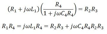
By separating the real and imaginary equation we get,
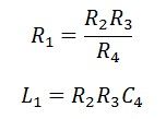
The above equation shows that the bridges have two variables R4 and C4 which appear in one of the two equations and hence both the equations are independent.
The circuit quality factor is expressed as
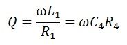
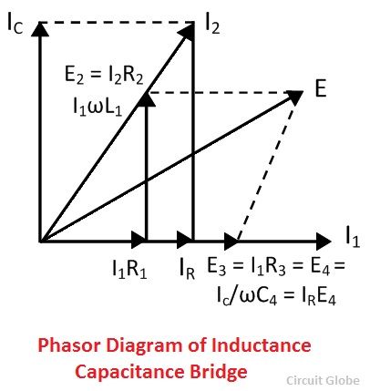
Phasor diagram of Maxwell’s inductance capacitance bridge is shown in the figure below.
Advantages of the Maxwell’s Bridges
The following are the advantages of the Maxwell bridges- The balance equation of the circuit is free from frequency.
- Both the balance equations are independent of each other.
- The Maxwell’s inductor capacitance bridge is used for the measurement of the high range inductance.
Disadvantages of the Maxwell’s Bridge
The main disadvantages of the bridges are- The Maxwell inductor capacitance bridge requires a variable capacitor which is very expensive. Thus, sometimes the standard variable capacitor is used in the bridges.
- The bridge is only used for the measurement of medium quality coils.
H-bridge paves new ways for LED lighting
The H-bridge is a classic circuit used for driving DC motors in a user-defined manner, such as in forward/reverse direction or PWM-assisted controlled RPM with the help of four discrete/integrated switches or electromechanical relays. It is widely employed in robotics and power electronics. This Design Idea is a novel implementation of this technique for driving white-LED arrays directly from the AC mains in full-wave current-limited mode to realize an excellent flicker-free, energy-efficient solid-state lamp. The circuit controls and maintains the LED excitation current in both negative and positive half cycles of the excitation voltage to a constant level by way of electronic switches operating alternately during the positive and negative excursion of the excitation voltage. This approach facilitates current-controlled rectification of AC voltage into a DC voltage for energizing series-connected LEDs with clean DC current with negligible ripple and substantially enhances the power factor.
As shown in Figure 1, transistors Q1, Q3, and Q5 and diode D4 as well as transistors Q2, Q4, and Q6 and diode D3 are configured as series-connected voltage-controlled current switches to form two arms of the H-bridge; diodes D1 and D2 form the other two arms of the bridge. The LED string is connected between the midpoints of the bridge designated as VLED+ and VLED GND, respectively. The AC is applied to the circuit through a current-limiting PTC resistor, R5; series-connected capacitors, C4 and C5 (configured as a nonpolar capacitor, CEFF); and inductor, L1. Likewise, the neutral side of the mains is connected to the circuit ground through an inductor, L2.

Figure 1 Current-limiting transistors and diodes route alternate AC half cycles to the series LED string.
During the positive half cycle, the AC
power bus becomes positive with respect
to the ground, and transistor Q1 gets
appropriate base bias through resistor
R1. Current flows through diode D4,
transistor Q1, and resistor R3, as illustrated
by arrow A1, and then through
the LED string comprising 12 medium-power
LEDs (LED1 to LED12) to the
ground through diode D2, as shown
by arrow A2. In a similar fashion, during the negative half cycle when the
ac power bus becomes negative with
respect to ground and transistor Q2 gets
base bias through resistor R2, the current
flows through diode D3, transistor Q2,
and resistor R4, as illustrated by arrow
A3, and then through the LED string
to the ac power bus through diode D1, as shown by arrow A4. In this way, during
a complete cycle the current flows
through the string in the same direction
and gets added up like you would get in
a full-wave bridge rectifier. However,
the magnitude of current ILED remains
constant as regulated by the respective
switches serving as voltage-controlled
current sources.As the base emitter junctions of transistors Q3 and Q4 are connected across current-sensing resistors R3 and R4, respectively, they turn on when the voltage drop across R3 and R4 increases beyond Q3 and Q4’s base emitter voltages. At this point, Q1’s and Q2’s bases are pulled down, disrupting the flow of current through them during respective half cycles of the ac mains. In this way, the current flowing through the transistors is kept constant and never allowed to go beyond a threshold, set by appropriately choosing the R3 and R4 values. Q5 and Q6 limit the base current of Q1 and Q2 to a safe value (around 150 μA) to ensure that they are never overdriven. The substantial parts of the base currents of Q1 and Q2 are shunted to R3 and R4 by means of Q5 and Q6 when their respective base emitter voltages exceed the potential drop across R6 and R8 connected in series with R1 and R2, respectively.
The magnitude of ac current flowing into the bus is limited by the reactance of CEFF (1/2πfCEFF) at the mains frequency and can be altered by appropriately choosing C4 and C5, configured as a nonpolar capacitor. The circuit can also be driven by a resistive supply by replacing CEFF with a suitable high-power resistor of 50 to 200Ω. This may facilitate an excellent power factor, but at the expense of very high power losses in the current-limiting resistor. R3 and R4 can be chosen appropriately as per the required constant-current magnitude. D5 protects the LED string from high reverse voltage, and R5 limits the inrush of current at turn-on. Inductors L1 and L2 and capacitor C1 help in minimizing the EMI/RFI besides improving the power factor. A metal oxide varistor can also be inserted in parallel with the AC mains to protect the circuit from transients.

Figure 2 VLED+ without capacitor C2 has ripple (a); VLED+ with capacitor C2 has reduced ripple (b).
In the circuit, 12 0.5W LEDs operate
at 120mA DC (135mA RMS) with
respect to current-sensing resistors R3
and R4, chosen as 1Ω. You can, however,
increase the number of LEDs to 18 as
long as the voltage being applied across
the string is more than the sum of the
forward voltage of the individual LEDs.
(White LEDs’ forward voltage varies
from 3.3 to 4V.) The voltage appearing
across the string is self-limiting (in
this case, it is around 42V) and does
not require any additional regulation,
since series-connected LEDs behave
like high-power zener diodes when
operated in forward-biased mode. The
circuit draws 11.5W power at 230VRMS and exhibits a power factor of
0.93 without any perceptible flicker in
the LEDs. You may optionally connect
a 220μF capacitor, C2, between VLED+
and VLED GND to further suppress ripple,
as shown in Figure 2. Alternatively,
the given string can be replaced by six
parallel-connected strings of LEDs,
each having 12 to 18 20mA
high-brightness LEDs. You must mount
transistors Q1 and Q2 on heat sinks to
avoid thermal runaway.Fontana bridge
A Fontana bridge is a type of bridge circuit that implements a wide frequency band voltage-to-current converter. The converter is characterized by a combination of positive and negative feedback loops, implicit in this bridge configuration. This feature allows compensation for parasitic impedance
 connected in parallel with the useful load
  , which in turn keeps an excitation current
  flowing through the useful load independent of the instantaneous value of . This feature is of great advantage for making electromechanical transducers.
If balance condition:


A Fontana bridge is a type of bridge circuit
that implements a wide frequency band voltage-to-current converter. The
converter is characterized by a combination of positive and negative
feedback loops, implicit in this bridge configuration. This feature
allows compensation for parasitic impedance connected in parallel with the useful load , which in turn keeps an excitation current flowing through the useful load independent of the instantaneous value of . This feature is of great advantage for making electromechanical transducers.
If balance condition:
connected in parallel with the useful load , which in turn keeps an excitation current flowing through the useful load independent of the instantaneous value of . This feature is of great advantage for making electromechanical transducers.
 Fontana Bridge
Zobel networks are a type of filter section based on the image-impedance design principle. They are named after Otto Zobel of Bell Labs, who published a much-referenced paper on image filters in 1923.[1]
The distinguishing feature of Zobel networks is that the input
impedance is fixed in the design independently of the transfer function.
This characteristic is achieved at the expense of a much higher
component count compared to other types of filter sections. The
impedance would normally be specified to be constant and purely
resistive. For this reason, Zobel networks are also known as constant
resistance networks. However, any impedance achievable with discrete
components is possible.
Zobel networks were formerly widely used in telecommunications
to flatten and widen the frequency response of copper land lines,
producing a higher-quality line from one originally intended for
ordinary telephone use. However, as analogue technology has given way
to digital, they are now little used.
When used to cancel out the reactive portion of loudspeaker impedance, the design is sometimes called a Boucherot cell. In this case, only half the network is implemented as fixed components, the other half being the real and imaginary components of the loudspeaker impedance. This network is more akin to the power factor correction circuits used in electrical power distribution, hence the association with Boucherot's name.
A common circuit form of Zobel networks is in the form of a bridged T. This term is often used to mean a Zobel network, sometimes incorrectly when the circuit implementation is, in fact, something other than a bridged T.

BBC engineers equalising audio landlines circa 1959. The boxes with
two large black dials towards the top of the equipment racks are
adjustable Zobel equalisers. They are used both for temporary outside
broadcast lines and for checking the engineer's calculations prior to
building permanent units
- Parts of this article or section rely on the reader's knowledge of the complex impedance representation of capacitors and inductors and on knowledge of the frequency domain representation of signals.
Derivation


 is simply the inverse, or dual impedance of
  .
.
The bridging impedance ZB is across the balance points and hence has no potential across it. Consequently, it will draw no current and its value makes no difference to the function of the circuit. However, its value is often chosen to be Z0 for reasons which will become clear in the discussion of bridged T circuits.
Input impedance
The input impedance is given by


Transfer function

Bridged T implementation


Types of section
A Zobel filter section can be implemented for low-pass, high-pass, band-pass or band-stop. It is also possible to implement a flat frequency response attenuator. This last is of some importance for the practical filter sections described later.Attenuator
Z and Z' for a Zobel attenuator


Low pass

Z and Z ' for a Zobel low-pass filter section


High pass
Z and Z' for a Zobel high-pass filter section


Band pass

Z and Z' for a Zobel band-pass filter section


Band stop

Z and Z' for a Zobel band-stop filter section


Practical sections

A transparent mask used to aid design of Zobel networks. The mask is
laid over a plot of the line response and the component values
corresponding to the closest fitting curve can be chosen. This
particular mask is for high-pass sections.
Basic loss
A practical high pass section incorporating basic loss used to correct high end roll-off
6 dB/octave roll-off

High-pass Zobel network response for various basic losses. Normalised to  and
and 
and
Mismatched lines
Quite commonly in telecomms networks, a circuit is made up of two sections of line which do not have the same characteristic impedance. For instance 150 Ω and 300 Ω. One effect of this is that the roll-off can start at 6 dB/octave at an initial cut-off frequency , but then at
  can become suddenly steeper. This situation then requires (at least)
two high-pass sections to compensate each operating at a different
can become suddenly steeper. This situation then requires (at least)
two high-pass sections to compensate each operating at a different  .
.
Bumps and dips
Bumps and dips in the passband can be compensated for with band-stop and band-pass sections respectively. Again, an attenuator element is also required, but usually rather smaller than that required for the roll-off. These anomalies in the pass-band can be caused by mismatched line segments as described above. Dips can also be caused by ground temperature variations.Transformer roll-off

Low frequency equaliser section with compensation for inductor resistance. The resistance r represents the stray resistance of the non-ideal inductor. The resistance r' is a real resistor calculated to compensate for r.
Low frequency sections will usually have inductors of high values. Such inductors have many turns and consequently tend to have significant resistance. In order to keep the section constant resistance at the input, the dual branch of the bridge T must contain a dual of the stray resistance, that is, a resistor in parallel with the capacitor. Even with the compensation, the stray resistance still has the effect of inserting attenuation at low frequencies. This in turn has the effect of slightly reducing the amount of LF lift the section would otherwise have produced. The basic loss of the section can be increased by the same amount as the stray resistance is inserting and this will return the LF lift achieved to that designed for.
Compensation of inductor resistance is not such an issue at high frequencies were the inductors will tend to be smaller. In any case, for a high-pass section the inductor is in series with the basic loss resistor and the stray resistance can merely be subtracted from that resistor. On the other hand, the compensation technique may be required for resonant sections, especially a high Q resonator being used to lift a very narrow band. For these sections the value of inductors can also be large.
Temperature compensation
An adjustable attenuation high-pass filter can be used to compensate for changes in ground temperature. Ground temperature is very slow varying in comparison to surface temperature. Adjustments are usually only required 2-4 times per year for audio applications.
A collection of various designs of temperature compensation equaliser.
Some can be adjusted with plugable links, others require soldering.
Adjustment is not very frequent.

The internal components of a temperature equaliser. The inductor and
capacitor on the right set the frequency at which the equaliser starts
to operate, the banks of selectable resistors on the left set the basic
loss and hence amount of equalisation.
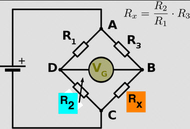
Kelvin Bridge
The Kelvin bridge or Thompson bridge is used for measuring the unknown resistances having a value less than 1Ω. It is the modified form of the Wheatstone Bridge.
What is the need of Kelvin Bridge?
Wheatstone bridge use for measuring the resistance from a few ohms to several kilo-ohms. But error occurs in the result when it is used for measuring the low resistance. This is the reason because of which the Wheatstone bridge is modified, and the Kelvin bridge obtains. The Kelvin bridge is suitable for measuring the low resistance.Modification of Wheatstone Bridge
In Wheatstone Bridge, while measuring the low-value resistance, the resistance of their lead and contacts increases the resistance of their total measured value. This can easily be understood with the help of the circuit diagram.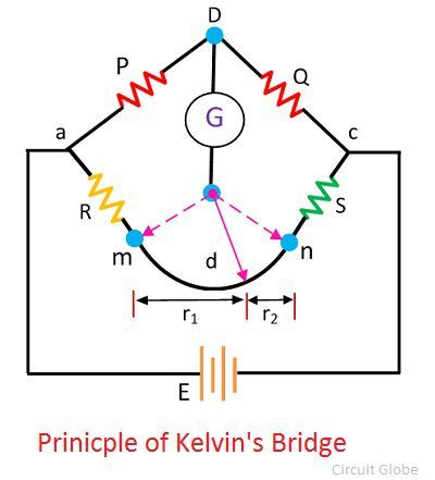
The r is the resistance of the contacts that connect the unknown resistance R to the standard resistance S. The ‘m’ and ‘n’ show the range between which the galvanometer is connected for obtaining a null point.
When the galvanometer is connected to point ‘m’, the lead resistance r is added to the standard resistance S. Thereby the very low indication obtains for unknown resistance R. And if the galvanometer is connected to point n then the r adds to the R, and hence the high value of unknown resistance is obtained. Thus, at point n and m either very high or very low value of unknown resistance is obtained.
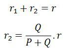
So, instead of connecting the galvanometer from point, m and n we chose any intermediate point say d where the resistance of lead r is divided into two equal parts, i.e., r1 and r2
The presence of r1 causes no error in the measurement of unknown resistance.
From equation (1), we get
as
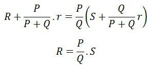
The above equation shows that if the galvanometer connects at point d then the resistance of lead will not affect their results.
The above mention process is practically not possible to implement. For obtaining the desired result, the actual resistance of exact ratio connects between the point m and n and the galvanometer connects at the junction of the resistor.
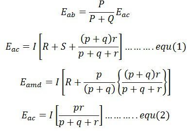
Kelvin Double Bridge Circuit
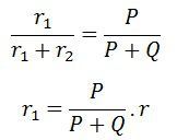
The ratio of the arms p and q are used to connect the galvanometer at the right place between the point j and k. The j and k reduce the effect of connecting lead. The P and Q is the first ratio of the arm and p and q is the second arm ratio.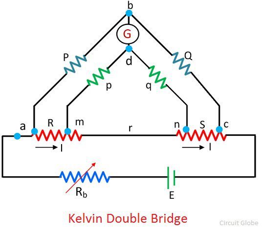
The galvanometer is connected between the arms p and q at a point d. The point d places at the centre of the resistance r between the point m and n for removing the effect of the connecting lead resistance which is placed between the unknown resistance R and standard resistance S.
The ratio of p/q is made equal to the P/Q. Under balance condition zero current flows through the galvanometer. The potential difference between the point a and b is equivalent to the voltage drop between the points Eamd.
Now,
For zero galvanometer deflection,
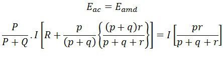
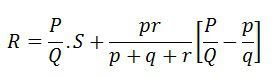
As we known, P/Q = p/q then above equation becomes

The above equation is the working equations of the Kelvins bridge. The equation shows that the result obtains from the Kelvin double bridge is free from the impact of the connecting lead resistance.
For obtaining the appropriate result, it is very essentials that the ratio of their arms is equal. The unequal arm ratio causes the error in the result. Also, the value of resistance r should be kept minimum for obtaining the exact result.
The thermo-electric EMF induces in the bridge during the reading. This effect can be reduced by measuring the resistance with the reverse battery connection. The real value of the resistance obtains by takings the means of the two.
Limitations of Kelvins Bridge
- The sensitive galvanometer is used for detecting the balance condition.
- The high measurement current is required for obtaining the good sensitivity.
Campbell’s Bridge
The bridge which measures the unknown mutual inductance regarding mutual inductance such type of bridge is known as the Campbell bridge. The mutual inductance is the phenomenon in which the variation of current in one coil induces the current in the nearer coil. The bridge also used for measuring the frequency by adjusting the mutual inductance until the null point is not obtained.
Consider the figure below shows the mutual inductance.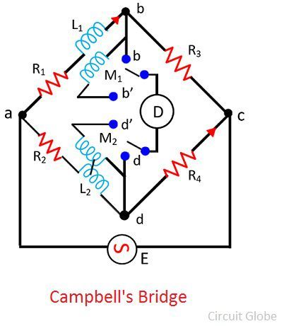
Let, M1 – unknown mutual inductance
L1 – self-inductance of secondary of mutual inductance M1
M2 – variable standard mutual inductance
L2 – self-inductance of secondary of mutual inductance M2
R1,R2,R3,R4 – non-inductive resistance
The two steps are required for obtaining the balanced position of the bridge.
1. The detector is connected between points ‘b’ and, ‘d’. The circuit behaves like a simple self-inductance commercial bridge. The condition requires for obtaining the balanced position of a bridge is
The bridge is in balanced condition by adjustment the R3 or R4 and R1 and R2.
2. The detector is connected between the b’ and d’. Along with the step-1 adjustment if the mutual inductance M2 is varied, then the balance point is obtained.
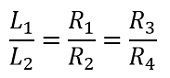
Anderson’s Bridge
The Anderson’s bridge gives the accurate measurement of self-inductance of the circuit. The bridge is the advanced form of Maxwell’s inductance capacitance bridge. In Anderson bridge, the unknown inductance is compared with the standard fixed capacitance which is connected between the two arms of the bridge.
Constructions of Anderson’s Bridge
The bridge has fours arms ab, bc, cd, and ad. The arm ab consists unknown inductance along with the resistance. And the other three arms consist the purely resistive arms connected in series with the circuit. The static capacitor and the variable resistor are connected in series and placed in parallel with the cd arm. The voltage source is applied to the terminal a and c.
Phasor Diagram of Anderson’s Bridge
The phasor diagram of the Anderson bridge is shown in the figure below. The current I1 and the E3 are in phase and represented on the horizontal axis. When the bridge is in balance condition the voltage across the arm bc and ec are equal.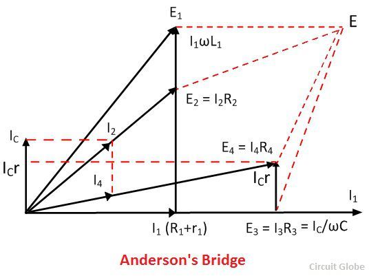
The current enters into the bridge is divided into the two parts I1 and I2. The I1 is entered into the arm ab and causes the voltage drop I1(R1+R) which is in phase with the I1. As the bridge is in the balanced condition, the same current is passed through the arms bc and ec.
The voltage drop E4 is equal to the sum of the IC/ωC and the IC r. The current I4 and the voltage E4 are in the same phase and representing on the same line of the phasor diagram. The sum of the current IC and I4 will give rise to the current I2 in the arm ad.
When the bridge is at balance condition the emf across the arm ab and the point a, d and e are equal. The phasor sum of the voltage across the arms ac and de will give rise the voltage drops across the arm ab.
The V1 is also obtained by adding the I1(R1+r1) with the voltage drop ωI1L1 in the arm AB. The phasor sum of the E1 and E3 or E2 and E4 will give the supply voltage.
Theory of Anderson Bridge
Let, L1 – unknown inductance having a resistance R1.R2, R3, R4 – known non-inductive resistance
C4 – standard capacitor
At balance Condition,
Now,
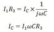
The other balance condition equation is expressed as
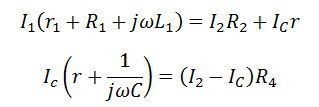
By substituting the value of Ic in the above equation we get,
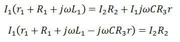
and
on equating the equation, we get
Equating the real and the imaginary part, we get
Advantages of Anderson Bridge
The following are the advantages of the Anderson’s Bridge.- The balance point is easily obtained on the Anderson bridge as compared to Maxwell’s inductance capacitance bridge.
- The bridge uses fixed capacitor because of which accurate reading is obtained.
- The bridge measures the accurate capacitances in terms of inductances.
Disadvantages of Anderson Bridge
The main disadvantages of Anderson’s bridge are as follow.- The circuit has more arms which make it more complex as compared to Maxwell’s bridge. The equation of the bridge is also more complex.
- The bridge has an additional junction which arises the difficulty in shielding the bridge.
Carey-Foster Slide-Wire Bridge
The Carey Foster Bridge is used for measuring the low resistance or for the comparison of two nearly equal resistances. The working principle of the Carey foster bridge is similar to the Wheatstone Bridge.
The circuit for the Carey foster bridge is shown in the figure below.
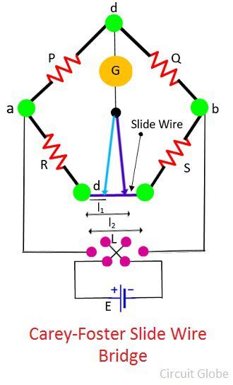
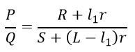
Let P, Q, R and S are the four resistors used in the bridge. The resistances of P and R are known while the R and S are the unknown resistors. The slide wire of length L is placed between the resistance R and S. The resistor P and Q are adjusted so that the ratio of P/Q is equivalent to the R/S. The ratio of the resistance is equivalent by sliding the contact on the sliding wiring.
Let l1 is the distance from the left at which the balanced is obtained. Now the R and S are interchanged, and this time the balanced is obtained by sliding the contact at the distance of l2.
Consider the equation for first balance
The r is the resistance per unit length of the sliding wire.
After interchanging the R and S, the balance equation of the bridge is
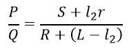
For the first balance equation
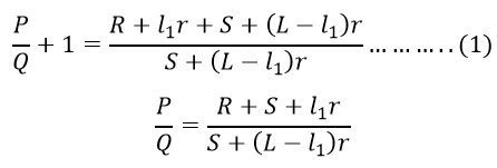
And for the second balance equation
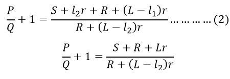
From equation (1) and (2)
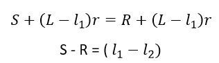
The difference between the resistance of S and R is obtained from a distance between the length of the slide-wire, i.e., l1 – l2 at balance condition.
Calibration of Slide Wire
The calibration of the sliding wire can be done by placing the resistance R or S in parallel with the slide wire of known resistance. Let S is known and S’ is its values when shunted by known resistance.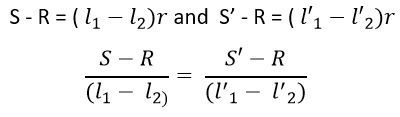
By solving the above equation, we get
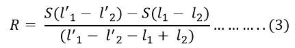
By the help of the Carey foster bridge, the direct comparison between the resistance R and S regarding length can be done. The resistance of other components like the resistance of P, Q and sliding contact are completely eliminated.
Note: The special switch is used for interchanging the resistor S and R during the test.
AC Bridge
The bridge uses for measuring the value of unknown resistance, inductance and capacitance, is known as the AC Bridge. The AC bridges are very convenient and give the accurate result of the measurement.
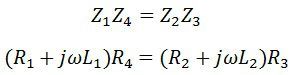
The construction of the bridges is very simple. The bridge has four arms, one AC supply source and the balance detector. It works on the principle that the balance ratio of the impedances will give the balance condition to the circuit which is determined by the null detector.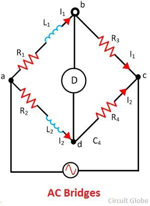
General Equation for an AC Bridge
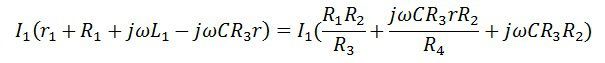
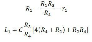
The bridges have four arms, two have non-inductive resistance and the other two have inductances with negligible resistance.When the bridge is in a balanced condition,
The l1 and R1 are the unknown quantities which are measured in terms of R2, R3, R4 and L2. From equation (1) and (2) the following points are concluded.
- The two balance equation is always obtained from the AC bridges.
- The unknown quantities are determined through the balanced equations. The unknown quantities are usually inductance, capacitance and resistance.
- The balance equations are independent of frequency.
The Basic of ROBOTICS ::: Hybrid Stepper Motor
The word Hybrid means combination or mixture. The Hybrid Stepper Motor is a combination of the features of the Variable Reluctance Stepper Motor and Permanent Magnet Stepper Motor. In the center of the rotor, an axial permanent magnet is provided. It is magnetized to produce a pair of poles as North (N) and South (S) as shown in the figure below.
At both the end of the axial magnet the end caps are provided, which contains an equal number of teeth which are magnetized by the magnet. The figure of the cross section of the two end caps of the rotor is shown below.
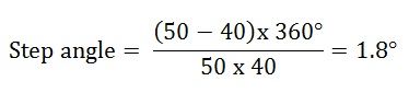
The stator has 8 poles, each of which has one coil and S number of teeth. There are 40 poles on the stator, and each end cap has 50 teeth. As the stator and rotor teeth are 40 and 50 respectively, the step angle is expressed as shown below.
The rotor teeth are perfectly aligned with the stator teeth. The teeth of the two end caps are displaced from each other by half of the pole pitch. As the magnet is axially magnetized, all the teeth on the left and right end cap acquire polarity as south and north pole respectively.
The coils on poles 1, 3, 5 and 7 are connected in series to form phase A. Similarly, the coils on the poles 2, 4, 6 and 8 are connected in series to form phase B.
When Phase is excited by supplying a positive current, the stator poles 1 and 5 becomes South poles and stator pole 3 and 7 becomes north poles.
Now, when the Phase A is de-energized, and phase B is excited, the rotor will turn by a full step angle of 1.8⁰ in the anticlockwise direction. The phase A is now energized negatively; the rotor moves further by 1.8⁰ in the same anti-clockwise direction. Further rotation of the rotor requires phase B to be excited negatively.
Thus, to produce anticlockwise motion of the rotor the phases are energized in the following sequence +A, +B, -A, -B, +B, +A…….. For the clockwise rotation, the sequence is +A, -B, +B, +A……..
One of the main advantages of the Hybrid stepper motor is that, if the excitation of the motor is removed the rotor continues to remain locked in the same position as before the removal of the excitation. This is because of the Detent Torque produced by the permanent magnet.
Advantages of Hybrid Stepper Motor
The advantages of the Hybrid Stepper Motor are as follows:-- The length of the step is smaller.
- It has greater torque.
- Provides Detent Torque with the de-energized windings.
- Higher efficiency at lower speed.
- Lower stepping rate.
Disadvantages of Hybrid Stepper Motor
The Hybrid Stepper Motor has the following drawbacks.- Higher inertia.
- The weight of the motor is more because of the presence of the rotor magnet.
- If the magnetic strength is varied, the performance of the motor is effected.
- The cost of the Hybrid motor is more as compared to the Variable Reluctance Motor.
Stepper Motor
Contents:
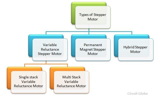
There are three types of stepping motor based on the rotor arrangements. They are as follows:-
The variable reluctance motor is divided into two types. They are known as Single stack variable reluctance motor and Multi-stack variable reluctance motor.
- Permanent Magnet (PM) Stepper Motor
- Hybrid Stepper Motor (combination of VR and PM type)
Step Angle in Stepper Motor
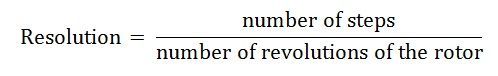
Definition: Step angle is defined as the angle which the rotor of a stepper motor moves when one pulse is applied to the input of the stator.The positioning of a motor is decided by the step angle and is expressed in degrees. The resolution or the step number of a motor is the number of steps it makes in one revolution of the rotor. Smaller the step angle higher the resolution of the positioning of the stepper motor.
The accuracy of positioning of the objects by the motor depends on the resolution. Higher the resolution greater will be the accuracy. Some precision motors can make 1000 steps in one revolution with a step angle of 0.36 degrees. A standard motor will have a step angle of 1.8 degrees with 200 steps per revolution. The various step angles like 90, 45 and 15 degrees are common in simple motors.
The number of phases can vary from two to six. Small steps angle can be obtained by using slotted pole pieces.
Advantages of Stepper Motor
The various benefits of the Stepping Motor are as follows:-- The motor is simple in construction, reliable.
- At the standstill condition, the motor has full torque.
- The motors are less costly.
- They require little maintenance.
- The stepper motor has an excellent and accurate starting, stopping and reversing response.
Disadvantages of Stepper Motor
The various disadvantages of the stepping motor are as follows:-- The motor uses more current as compared to the DC motor.
- At the higher speed, the value of torque reduces.
- Lower efficiency.
- The Resonance condition arises and requires micro stepping.
- At the high speed, the control is not possible.
Stepper Motor Applications
- As the stepper motor are digitally controlled using an input pulse, they are suitable for use with computer controlled systems.
- They are used in numeric control of machine tools.
- Used in tape drives, floppy disc drives, printers and electric watches.
- The stepper motor also use in X-Y plotter and robotics.
- It has wide application in textile industries and integrated circuit fabrications.
- The other applications of the Stepper Motor are in spacecrafts launched for scientific explorations of the planets etc.
- These motors also find a variety of commercial, medical and military applications and also used in the production of science fiction movies.
- Stepper motors of microwatts are used in the wrist watches.
- In the machine tool, the stepper motors with ratings of several tens of kilowatts is used
Advantages of Stepper Motor:
- The rotation angle of the motor is proportional to the input pulse.
- The motor has full torque at standstill.
- Precise positioning and repeatability of movement since good stepper motors have an accuracy of 3 – 5% of a step and this error is non cumulative from one step to the next.
- Excellent response to starting, stopping and reversing.
- Very reliable since there are no contact brushes in the motor. Therefore the life of the motor is simply dependant on the life of the bearing.
- The motors response to digital input pulses provides open-loop control, making the motor simpler and less costly to control.
- It is possible to achieve very low speed synchronous rotation with a load that is directly coupled to the shaft.
- A wide range of rotational speeds can be realized as the speed is proportional to the frequency of the input pulses.
Applications:
- Industrial Machines – Stepper motors are used in automotive gauges and machine tooling automated production equipments.
- Security – new surveillance products for the security industry.
- Medical – Stepper motors are used inside medical scanners, samplers, and also found inside digital dental photography, fluid pumps, respirators and blood analysis machinery.
- Consumer Electronics – Stepper motors in cameras for automatic digital camera focus and zoom functions.
Operation of Stepper Motor:
Stepper motors operate differently from DC brush motors,
which rotate when voltage is applied to their terminals. Stepper
motors, on the other hand, effectively have multiple toothed
electromagnets arranged around a central gear-shaped piece of iron. The
electromagnets are energized by an external control circuit, for example
a microcontroller.
To make the motor shaft turn, first one
electromagnet is given power, which makes the gear’s teeth magnetically
attracted to the electromagnet’s teeth. The point when the gear’s teeth
are thus aligned to the first electromagnet, they are slightly offset
from the next electromagnet. So when the next electromagnet is turned ON
and the first is turned OFF, the gear rotates slightly to align with
the next one and from there the process is repeated. Each of those
slight rotations is called a step, with an integer number of steps
making a full rotation. In that way, the motor can be turned by a
precise. Stepper motor doesn’t rotate continuously, they rotate in
steps. There are 4 coils with 90o angle between each other
fixed on the stator. The stepper motor connections are determined by the
way the coils are interconnected.In stepper motor, the coils are not
connected together. The motor has 90o rotation step with the
coils being energized in a cyclic order, determining the shaft rotation
direction. The working of this motor is shown by operating the switch.
The coils are activated in series in 1 sec intervals. The shaft rotates
90o each time the next coil is activated. Its low speed torque will vary directly with current.
Stepper Motor Control by Varying Clock Pulses
Stepper motor control circuit is a
simple and low-cost circuit, mainly used in low power applications. The
circuit is shown in figure, which consist 555 timers IC as stable
multi-vibrator. The frequency is calculated by using below given
relationship:
Frequency = 1/T = 1.45/(RA + 2RB)C Where RA = RB = R2 = R3 = 4.7 kilo-ohm and C = C2 = 100 µF.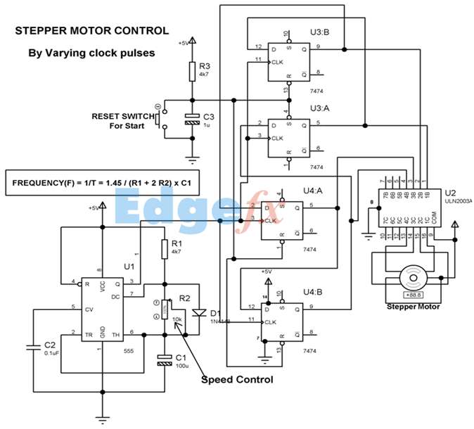
The output of timer is used as clock for
two 7474 dual ‘D’ flip-flops (U4 and U3) configured as a ring counter.
When power is initially switched on, only the first flip-flop is set
(i.e. Q output at pin 5 of U3 will be at logic ‘1’) and the other three
flip-flops are reset (i.e. output of Q is at logic 0). On receipt of a
clock pulse, the logic ‘1’ output of the first flip-flop gets shifted to
the second flip-flop (pin 9 of U3). Thus logic 1 output keeps shifting
in a circular manner with every clock pulse. Q outputs of all the four
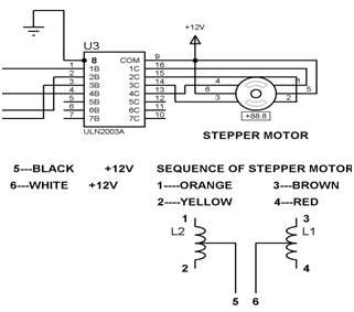
flip-flops are amplified by Darling-ton transistor arrays inside ULN2003
(U2) and connected to the stepper motor windings orange ,brown, yellow,
black to 16, 15 ,14, 13 of ULN2003 and the red to +ve supply.
The common point of the winding is
connected to +12V DC supply, which is also connected to pin 9 of
ULN2003. The color code used for the windings is may vary form make to
make. When the power is switched on, the control signal connected to SET
pin of the first flip-flop and CLR pins of the other three flip-flops
goes active ‘low’ (because of the power-on-reset circuit formed by R1-C1
combination) to set the first flip-flop and reset the remaining three
flip-flops. On reset, Q1 of IC3 goes ‘high’ while all other Q outputs go
‘low’. External reset can be activated by pressing the reset switch. By
pressing the reset switch, you can stop the stepper motor. The motor
again starts rotating in the same direction by releasing the reset
switch.
XO___XO +DW DW Electronic Bridges Information
- inductance
- capacitance
- admittance
- conductance
- impedance

ypes
There are many types of electronic bridges. Examples include a Wheatstone circuit bridge, an H circuit bridge, and a network bridge.- Wheatstone circuit bridges are electrical bridge circuits that are used to measure resistance. Wheatstone circuit bridges consist of a common electric current source such as a battery and a galvanometer, which connects two parallel branches, containing four resistors and the values of three resistors are known.
- An H circuit bridge has the capability to drive the motor forward or backward at any speed. An H circuit bridge can optionally use a completely independent power source.
- A network bridge is an inexpensive method to connect LAN segments. Other electronic bridges are commonly available.
Features
There are several ways in which electronic bridges function. Electric bridges are employed for interfacing transducers and helping to measure impedance at high frequencies. Wheatstone circuit bridges are suitable for measuring any small change in resistance. Wheatstone circuit bridges consist of two parallel branches where one branch contains a known resistance and an unknown resistance, while the other parallel branch contains resistors of known values. This circuit measures the value of the unknown resistor by adjusting the values of the other three resistances until the current passing through the galvanometer decreases to zero. In an H circuit bridge, a condition called "shoot through" exists where there is a path between the positive and the negative sides of the H bridge that can make semiconductors ballistic. A network bridge is a type of electric bridge that connects two sides of adjacent networks. A network bridge is also called a network switch. Electronic bridges are designed and manufactured to meet most industry specifications.Applications
Electronic bridges are used in many applications. Some examples include measurement of impedance, capacitance, conductance, and very high and very low resistance .Basic Variable Speed Motor/Switch
We like to construct a simple set-up where I either turn the knob or move a lever varying degrees to get varying speeds from a low-powered rotary electric motor. The effect I desire is similar to a De Walt cordless drill (which I am personally very familiar with as a window and door installer). I would like the motor to operate at these somewhat precise varying speeds when I move the lever one way, but is it easy to then get it to reverse rotating direction with the same lever, with the same precision, or should I just incorporate another motor into this system? If you would answer this please understand that I am not an electrician or an electro-anything, and I only have the most basic understanding of these concepts, so please answer accordingly (condescension is ok). Figure 1 is the "lever switch". Figure 2 is the variable speed motor. Please don't mock my artwork.

Other bridge features also considered
Bridge sensitivity is an issue that must be considered when observing
the bridge output. It is usually specified in mV/V, and is the value of
bridge output when the bridge is excited with one volt and the sensor is
at full scale. Typical sensitivity values are 1 to 2 mV/V. Accuracy of a
standard bridge is usually between 0.1 and 1% before any calibration is
performed.
Power dissipation is also an issue, as it is a function of bridge
voltage and arm resistance. A higher excitation voltage produces a
higher output, which is good, but results in higher dissipation. This
dissipation affects low-power operation, obviously, but also induces
increased self-heating of the bridge elements. Even though the bridge is
self-compensating for temperature drift to a large extent, it can
become a problem if the different elements are not thermally coupled and
at the same temperature.
The output of the bridge is not grounded, so any
conditioning/amplification circuitry must be isolated (Reference 2) or
have a differential input. Also, some sensors perform better using AC
rather than DC excitation, which can then be demodulated synchronously
to eliminate second- and third-order errors. 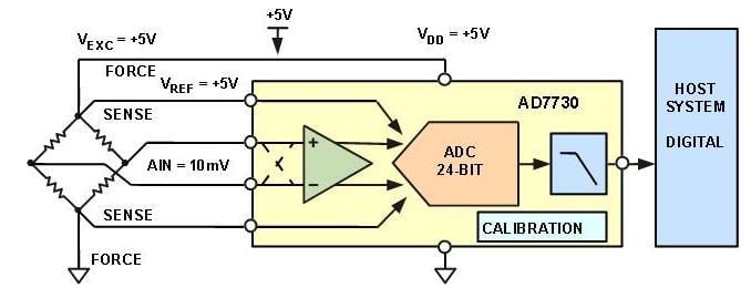 A
bridge interface IC such as the AD7730 provides all necessary
interface, amplification, scaling, calibration, and digital I/O along
with easy-to-use, high-resolution performance. Image source: Analog
Devices, Inc.
A
bridge interface IC such as the AD7730 provides all necessary
interface, amplification, scaling, calibration, and digital I/O along
with easy-to-use, high-resolution performance. Image source: Analog
Devices, Inc.
Due to the widespread use of bridge circuits and their many benefits,
IC vendors have developed many specialized interface devices which
simplify using them, setting amplifier gain, and minimizing various
residual error sources. For example, the AD7730 from Analog Devices,
Figure 4, can be configured for AC or DC excitation, provides a
user-settable differential amplifier followed by 24-bit A/D conversion,
and provides the resultant data in various serial formats to the system
microcontroller. Despite its internal complexity, it provides an
easy-to-use bridge excitation and interface function along with
filtering, calibration, and many other user options.
The simple yet clever bridge topology has been a valuable configuration
and tools since the earliest days of development of the principles of
basic electrical circuits. Despite its age, it is very often still the
best solution to the ongoing challenge of precisely matching a unknown
component against a known one, or capturing small changes in a sensor
output despite noise, component imperfections, and supply variations.
Implementing the Bridge Design with a Dual Op AmpWhat if the amplifier used in Figure 4 needs only one power supply and is capable of outputting bipolar voltages? Some single-supply amplifiers need headroom above ground, but a device that provides a true-zero output may be a fit for bridge sensors (Figure 6). A possibly ideal dual op-amp for this application integrates charge-pump circuitry that generates the negative voltage rail in conjunction with external capacitors. This allows the amplifier to operate from a single +4.5 V to +15 V power supply, but it is as effective as a normal dual-rail ±4.5 V to ±15 V amplifier.
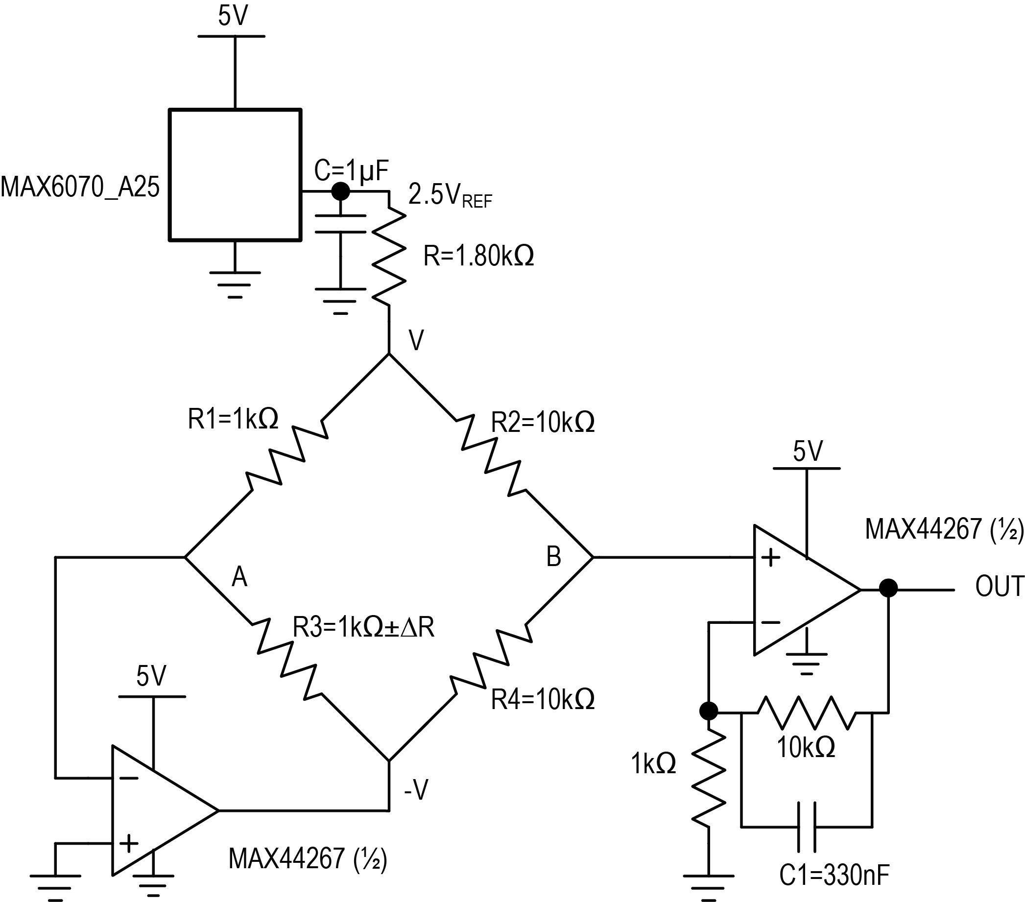 Figure 6. The MAX44267 precision, low-noise, low-drift, dual op amp offers a true-zero output from a single supply.
One such amplifier is the MAX44267, which can be implemented in the circuit of Figure 6 with just one supply voltage (positive supply, VCC). The integrated negative VSS generator or charge pump generates a negative supply voltage. This architecture provides an advantage to the designer, because it eliminates the need for negative supply regulators and reduces board layout space and cost.
Figure 7 includes a voltage reference to generate a 2.5 VOUT reference. A dual op amp is used with the resistance bridge where R1 = R3 = 1 kW and R2 = R4 = 10 kW. An additional 1.8 kW is used in series to reduce the amount of current flowing through the bridge and to reduce power dissipation. The V(+) node becomes one-third the voltage reference’s output at a balanced condition. This is followed with second-stage amplification having a gain of 11 at the OUTA node.
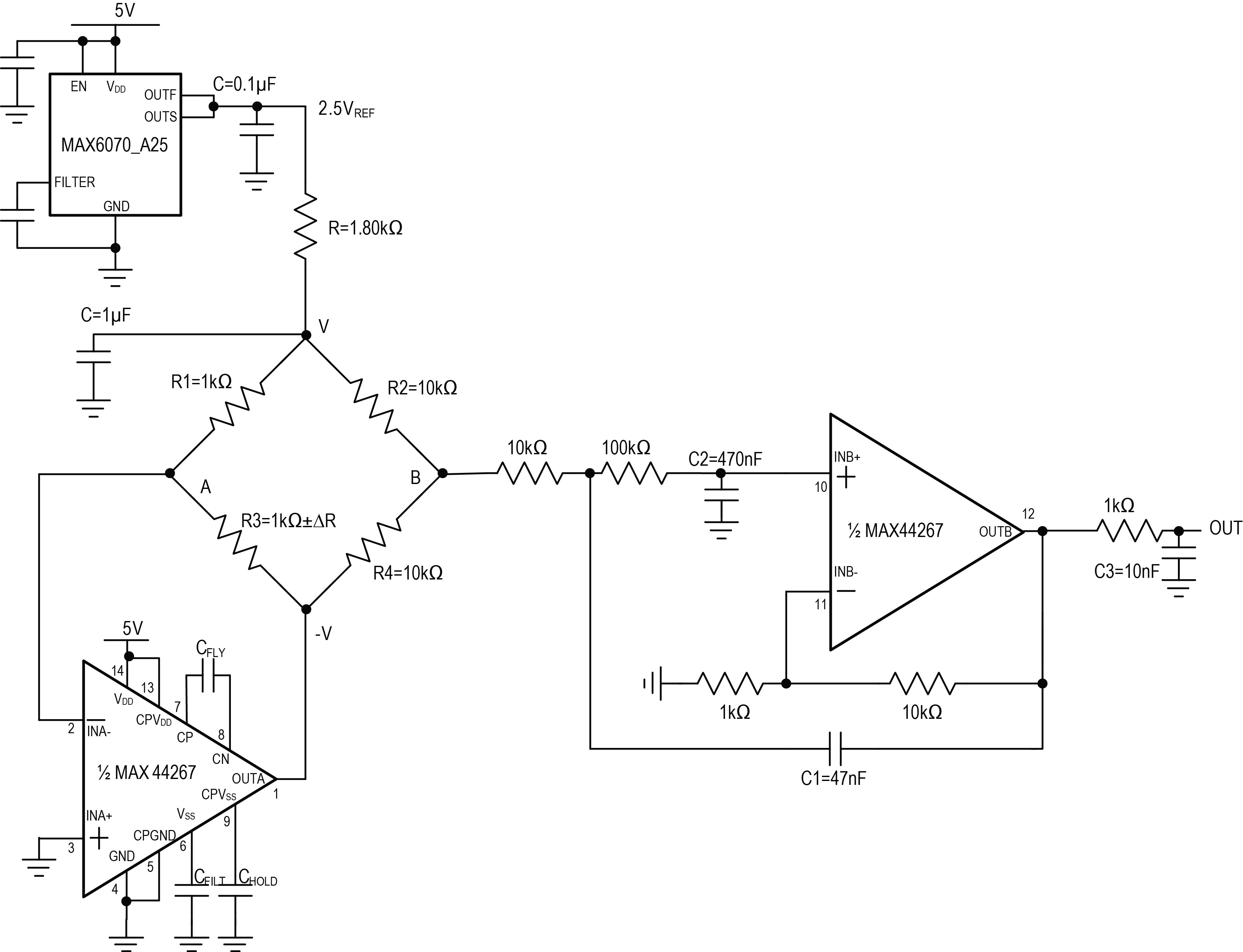 Figure 7. The MAX44267 op amp operates from a single supply.
 A Fluke RTD calibrator was used as the temperature-dependent resistance element (as PT1000) in place of R3; a temperature change from -50 C to +155 C is evaluated. For the given temperature change using a PT1000, the change in resistance(DR) is about 800 W and an equivalent range of 325 mV is effected (see Equation 4). Because amplifier 2 has an internal negative supply, it can accommodate this swing (-242mV to -83mV) at its input below ground, and it provides an output gain of 11.
Figure 7 utilizes a Sallen-Key filter in the second stage to filter the input signal to the required bandwidth (50Hz used in this case). Full-scale error accuracy within ±0.05% is obtained from the bridge output at node B without any calibration or trim. In this way the transfer function of the bridge circuit is made linear; improved performance of the front-end circuit is realized using MAX44267 in the subsequent section.
Test Measurements
1.Figure 8 shows the absolute bridge voltage output versus change in resistance (a linearity curve output), under 0.02%.
 Figure 8.The transfer curve shows the absolute voltage output vs. temperature for the Figure 7 circuit.
2. Figure 9 shows the gain error plot as percentage versus full-scale. The error curve shows small wriggles, in order of 0.002%, that are a combination of manual data plotting and measurement setup noise.
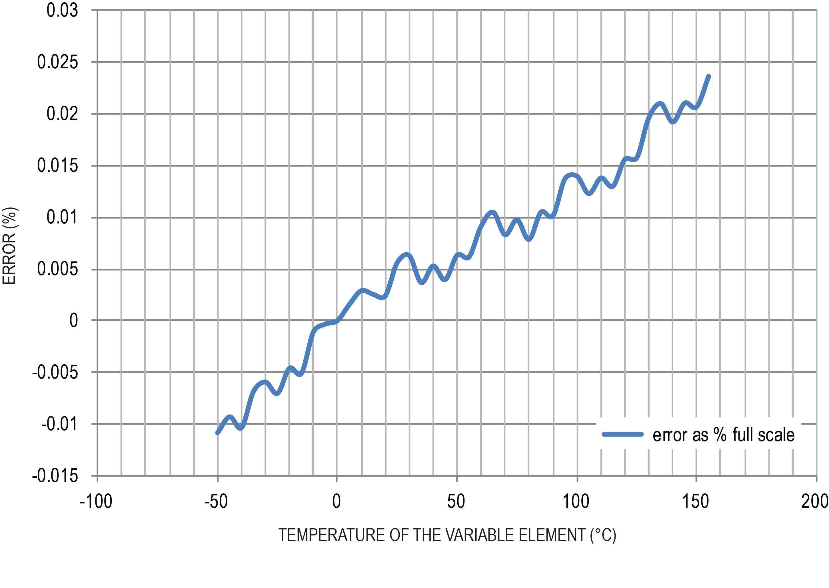 Figure 9. Error % vs. full scale for the circuit in Figure 7.
3. Figure 10 shows the voltage noise density of the bridge plus amplifier: 115nV/ÖHz at 1kHz and 500nV/ÖHz under 50Hz. A 50 Hz filter was implemented in the second stage to remove the sensitivity to line noise.
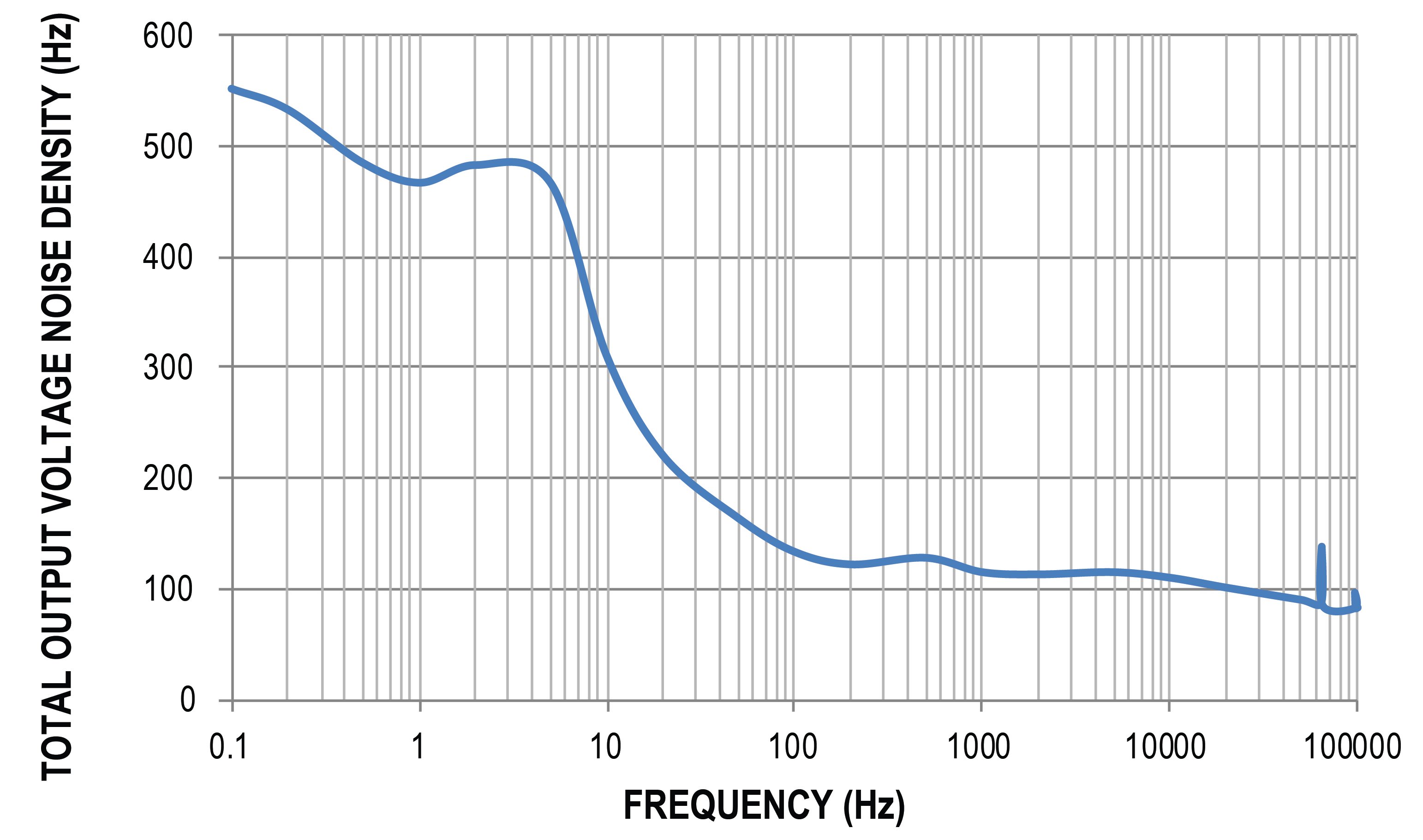 Figure 10. Output noise density vs. frequency for the circuit in Figure 7.
4. Figure 11 shows the voltage noise(VP-P) of the bridge plus amplifier, 0.1Hz to 10Hz, 6mVP-P

Figure 11. Peak-to-peak voltage noise from 0.1Hz to 10Hz for the circuit in Figure 7.
A fragment of a computer motherboard with a north bridge and connectors

How to Build an H-bridge Circuit to Control 4 Motors
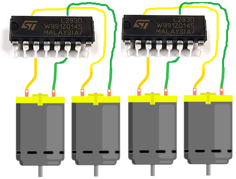
An H-bridge chip such as the L293/SN754410 can control up to 2 motors.
So in order to control 4 motors, we will need to use 2 H-bridge chips and tie them together.
We will build a circuit where all the motors are
synchronized, meaning they act in symphony. Thus, if we input so that
forward motion is activated,
all the motors will spin in a forward direction. If we input reverse
mode, all the motors will spin in reverse direction. So the motors act
in concert.
This type of circuit is useful for any circuit that
needs multiple motors. A common electronic device that now uses 4 DC
motors are flying drones.
If you go into amazon or any various online retailers to get a toy
drone, the majority of them use 4 motors, the 4 of which act in concert.
So this type of circuit
has very valuable use in the real world.
In actuality, you could use how many motors you want.
Since each H-bridge chip can operate 2 motors, then if you wanted to
have 8 motors running, then
you would need 4 H-bridge chips. If you want 16 motors running, then we
need 8 H-bridge chips. You would just have to know how to connect them
together, which is
relatively simple. It's like just cascading them in a sequence.
But in this circuit, we do 4 motors.
The motor operation is
Components
- 2 L293/SN754410 H-bridge Chips
- 4 DC Motors
- 2 Pushbutton Switches
- 1 Toggle Switch
- 2 10KΩ resistors
- Power Source
The L293/SN754410 H-bridge chip is 16-pin chip that can be used to drive and control
inductive loads such as relays, solenoids, DC motors, and bipolar stepper motors.
In this circuit, we will be using it to control 2 DC motors.
The L293/SN754410 is a relatively inexpensive chip that can be obtained for a little over $1.
One place that sells the L293 is
Tayda Electronics- L293 Driver IC.
Before we build this circuit, you must understand the chip and all of its pin connections.
You must always know pin connections when hooking up any chip.
Overall, the L293/SN754410 chips aren't very as complicated as they may seem. They both have identical
pinouts.
The pinout of the L293/SN754410 is shown below.
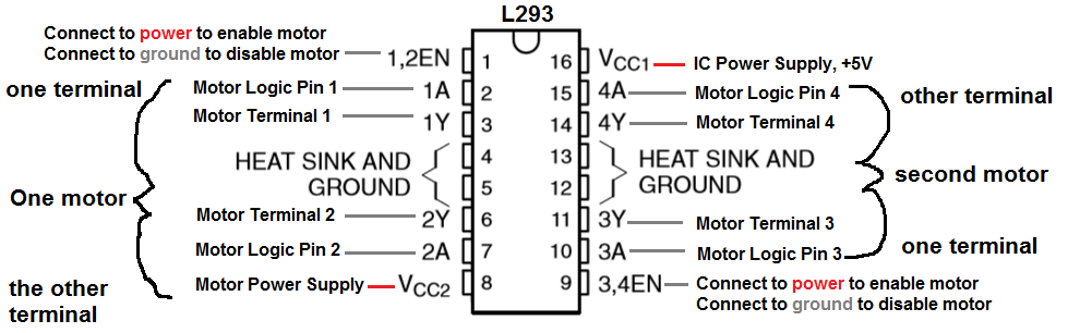
The L293/SN754410 is capable of controlling 2 motors.
It is a 4-channel H-bridge, meaning it can connect 4
terminal wires from motors. Since each motor has 2 terminals, it can
control 2 motors (2x2=4).
Pin 1 is the enable pin for terminals 1 and 2.
It enables motor to turn on when it is connected to a power. And
disables the motor from functioning
when connected to ground.
Pin 2 is the motor logic pin for terminal 1.
This is the voltage level which one of the motor terminals receive. The
logic level will
determine what action the motor will take. This is one of the two logic
levels that determines the function of the motor connected.
Pin 3 is the pin where we connect one of the terminals of the motor to.
Pin 4 and Pin 5 both get grounded.
Pin 6 is where we connect the other motor
terminal to. This completes the 2-terminal connections necessary for a
motor to be hooked up
to the H-bridge IC.
Pin 7 is the motor logic pin for terminal 2.
This is the second voltage signal we feed to the motor to determine the
action the motor will take.
Pin 8 is the pin which receives the voltage
needed to power on the motor. It is the motor power pin. This is the
pin where we place the positive
voltage of the power supply that will operate the DC motor. So if the
motor is a 9V motor, then you will need to feed 9V into this pin. If the
motor is a 12V motor,
then you will need to feed 12V into this pin.
Pin 9 is the enable pin for terminals 3 and 4.
It enables the motor to turn on when connected to power and disables the
motor when connected to
ground.
Pin 10 is the motor logic pin for terminal 3.
This is one of the logic voltage signals that determines the action that
the second motor will take.
Pin 11 is the pin where we connect one of the terminals of the second motor to.
Pin 12 and Pin 13 both get grounded.
Pin 14 is the pin where we connect the other terminal of the second motor to.
Pin 15 is the motor logic pin for terminal 4.
It is the second voltage signal that we feed into the second motor to
determine the action the motor
will take.
Pin 16 is the pin which receives the voltage
needed for power for the IC. It is the IC power pin. The IC needs just
about 5V in order to operate.
Therefore, we feed 5V into this pin.
These are all the pins of the motor. Once power is
supplied to the IC and the motor and all the terminals of the motor are
connected, then the pins
which determine how the motors will operate are the logic levels that we
feed into it.
The logic levels determine what action the motor will take.
A breakdown of logic levels and the resultant motor action are shown in the table below.
| Enable | Logic Pin 1 | Logic Pin 2 | Result |
| High | Low | High | Forward |
| High | High | Low | Reverse |
| High | Low | Low | Stop |
| High | High | High | Stop |
| Low | Doesn't matter | Doesn't matter | Off |
When the enable pin is high and the motor is fed a LOW
voltage signal at the first pushbutton and a HIGH voltage signal at the
second pushbutton,
then
the motors will spin forward. When the enable is high and the motor is
fed a HIGH voltage signal at the first pushbutton and a LOW voltage
signal at the second
pushbutton, then
the motors will spin in reverse. And with both logic levels at the same
level (2 HIGHs or 2 LOWs), then the motors will stop spinning.
4-Motor H-bridge Circuit
The H bridge circuit we will build to control 4 motors is shown below.
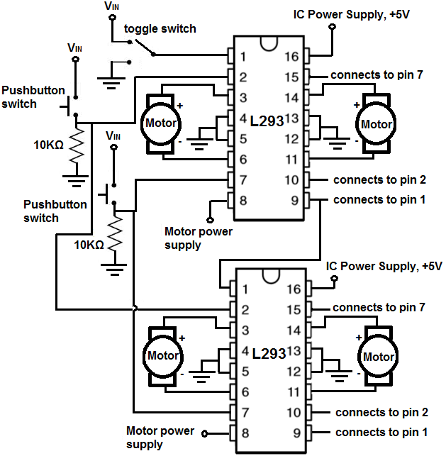
This above circuit built on a breadboard is shown below.
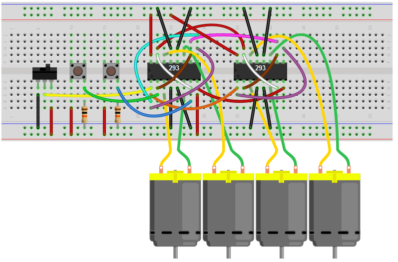
How this circuit works is based on the 2 switches that control the logic state and the 1 enable switch.
All the motor logic pins are tied together for each of
the motors, so the 2 pushbuttons control the logic state for all the 4
motors. Thus, this is why
they act in concert. So the first pushbutton controls the first logic
state for each of the motors. And the second pushbutton controls the
second logic state of
each of the motors.
So with the motor logic pins normally LOW, if we press down on the second button while leaving the first
one unpressed,
then the motors will spin in a forward.
Now if we press down on the first pushbutton while leaving the second one unpressed, the motors will spin
in the reverse direction.
If we leave both unpressed or press down on both simultaneously, the motors will not spin.
And this is all that is necessary for the operation of our 4-motor device.
To wire it up, it's pretty simple. For each chip, we connect terminals 1 and 3 and then
connect terminals 2 and 4. This way, both motors of
a chip are synched in together in a given chip. After this, for each additional chip we do the same, and then tie in
the the logic pins of the chip before into the chip after, so that all logic pins are connected together.
How to Build an H bridge Circuit with Transistors
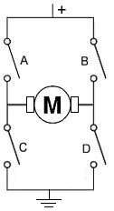
In this circuit, we will show how to build an H-bridge circuit with transistors.
An h bridge is a circuit that is used primarily to
control motors; they allow for forward and reverse motion of the motors.
Therefore, the motor can be utilized with its full
bidirectional capability.
To build an H-bridge, the only option is not to use an
IC chip for an H-bridge. You can also build it with discrete and simple
components such as with transistors and
resistors.
Even though it's almost invariably simpler to use an
IC to act as an H-bridge such as the popular L293 IC, there may be times
you may want to design one yourself for any
various reasons. You may also just be interested in knowning how an h
bridge works.
So in this circuit, we will build an H-bridge simply with bipolar junction transistors.
Since motors run off a good amount of current, we will
use high-current gain and high-power transistors. These are transistors
provide very good current gain and transistors
that deal with a lot of power.
In total, we use 4 different transistors, 2 PNP transistors and 2 NPN transistors.
The 2 types of transistors we will use are the TIP107
PNP transistors and the TIP102 NPN transistors. These are darlington
transistors that can deal with high power outputs. Again,
since motors require a good amount of current, normally about 75mA or
so, we want a high-power transistor. Motors require several times more
current than an output device that say an LED
would. We will talk about these transistors more.
Know that h bridges are useful for circuits that require bidirectional
functioning. Otherwise, the only way to be able to operate the device bidirectionally
would be to manually switch the polarity leads of the device. An H-bridge eliminates this
need.
So, again, h bridges can be used for any type of bidirectional 2-lead device
that works in opposite directional depending on which lead is connected to power.
It's mostly for motors, but it can also be for other devices as well.
Components
- 2 TIP107/127 PNP transistors
- 2 TIP102/120 NPN transistors
- 4 1KΩ resistors
- 2 5.6KΩ resistors
- DC motor
Really any NPN transistors or PNP transistors can be used.
But it is better for them to be high-power transistors, since motors
need adequate current.
The TIP107/127 transistors are PNP darlington transistors.
Being that they are a darlington transistors, they provide high
current gain. They also can deal with high power. The collector of the TIP107 transistor
can deal with up to 80 watts of power, while the TIP127 can deal with up to 65W.
Being that the highest-rated DC motors are
normally 12V, this means that the collector can pass 6.7A. Obviously, the motor
requires nothing close to this. We need less than 100mA. So this transistor is well
above the same range in power that we need.
The datasheets for the TIP107 or the TIP127 can be found at the following
links:
TIP107 PNP Datasheet and
TIP127 PNP Datasheet.
The TIP102/TIP120 transistors are NPN darlington transistors.
Being darlington transistors, they also provide high current gain.
This is good so that they can drive a high-power device such as a motor. The transistors
themselves can deal with high power.
The datasheets for the TIP102 or the TIP120 can be found at the following links:
TIP102 NPN Datasheet and
TIP120 NPN Datasheet.
Again, you can really use any NPN or PNP transistors.
High-power ones are better for this circuit, as motors need more, but
you can mix
and match and see what works.
The DC motor can be any type, of really any voltage. We are using
a 6-12V DC power supply, so the maximum rating the motor should have is 12V.
Normally, anyway, DC motors aren't rated higher than 12V, so you can use practically
any motor.
Besides these, all we need else are resistors.
H Bridge Circuit Built with Transistors
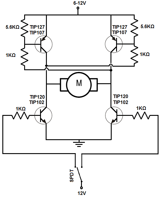
So the first thing that should be done is setting up power
for the circuit. The circuit operates off of 6-12V, so it
can run any type of motor. However, if you are using a much lower
voltage-rated DC motor such as a 3V, you can use lower voltage.
The circuit is manually controlled through a single pole double throw (SPDT) switch, a toggle switch.
The positive voltage either powers the base of the transistor on the left or the right. This transistor
that gets the positive voltage turns on.
This turns on the transistor on top on the other side.
Thus, if we turn on the left transistor, current flows from the right of the power source through
the transistor on the top right, through the DC motor from right to left, and then from the left transistor to ground.
If we flip the toggle switch to the other side, the bottom right transistor will be powered on. This
turns on the transistor at the top on the left side. Current flows from the power source, through the leftmost
transistor at the top, through the DC motor, from left to right, and through the rightmost transistor and down to ground.
Therefore, the circuit functions as an H-bridge.
If the switch is flipped one way, the motor spins in one direction.
If the switch is flipped the other way, the motor spins in the other direction.
So the circuit is able to achieve bidirectionality of the motor, as an h bridge should.
Normally, we would put diodes in reverse biased across the transistors. These diodes would help dampen transient spikes
that are generated by the motor's coils so that they do not damage other components in the circuits. When a transistor
stops running, it can create reverse emf, transient voltage spikes that can be large. To prevent them, reverse biased
diodes would stop these spikes from proceeding to other parts of the circuit, where they could cause damage. Being
we're flipping the transistors on and off by flipping the toggle switch, you do want to have protection against
back emf.
A SPDT switch is used for manual control to demonstrate how the circuit works. It is perfect because it only
allows one of the NPN transistors to be on at any given time. Both transistors cannot be on at the same time because
both transistors would have current flowing through, which is like a forbidden state. Therefore, it should be avoided.
A SPDT switch avoids this condition.
The circuit, as is, will never be off unless the power supply is removed, being that the SPDT has no
switch in which both transistors are grounded. To counter this, you could add a switch to the power supply so that
the power supply disconnects from the circuit, if this is desired.
If you don't want the circuit to be manually controlled by a switch, you can remove the SPDT switch
and instead
connect the base of the NPN transistors to whatever device you want to control it, such as a microcontroller. You
still keep the 1KΩ resistors at the base.
Another thing is that this circuit, as if, puts the DC motor at one speed. To vary the speeds,
instead of inputting a fixed DC voltage to the base of the transistors, a pulse width modulated signal would be
applied to the base. We won't get into this article what value of PWM signal you would need to achieve a given
speed, but you can take this approach to vary the speed of the DC motor. This is a far more efficient way than
using a potentiometer to vary the speed, which is inefficient since it creates large power waste, though you can still
use it.
So this is how an h bridge circuit can be built with transistors.
XO__XO +DW DW SAW Different Networking Devices And Hardware Types — Hub, Switch, Router, Modem, Bridge, Repeater

Short Bytes: Different networking devices have
different roles to play in a computer network. These network devices
also work at different segments of a computer network performing
different works. In our new series after network topology, we talk about
different networking devices like a switch, router, hub, bridge etc.
Computer
networking devices are known by different names such as networking
devices, networking hardware, network equipment etc. However, all of the
names mean the same but have got different purposes. After covering
different topics on network topologies and their advantages and
disadvantages, we are here once again with a series on the network
devices. Before we talk more about the networking devices, here are a few topics you might want to take a look at that we covered under network topology section:
- Daisy chaining in computer networks
- Different network topologies
- Tree topology
- Mesh Topology
- Star Topology
- Ring Topology
- Bus topology
For example:
A LAN cable has got the purpose of connecting a computer to the local area network, a Wi-Fi router has got the purpose of sending and receiving data between you and your internet connection. Similarly, we can think of other network devices with different purposes to serve.
Different networking devices:
Network Hub:
Network Hub is a networking device which is used to connect multiple network hosts. A network hub is also used to do data transfer. The data is transferred in terms of packets on a computer network. So when a host sends a data packet to a network hub, the hub copies the data packet to all of its ports connected to. Like this, all the ports know about the data and the port for whom the packet is intended, claims the packet.However, because of its working mechanism, a hub is not so secure and safe. Moreover, copying the data packets on all the interfaces or ports makes it slower and more congested which led to the use of network switch.
Network Switch:
Like a hub, a switch also works at the layer of LAN (Local Area Network) but you can say that a switch is more intelligent than a hub. While hub just does the work of data forwarding, a switch does ‘filter and forwarding’ which is a more intelligent way of dealing with the data packets.So, when a packet is received at one of the interfaces of the switch, it filters the packet and sends only to the interface of the intended receiver. For this purpose, a switch also maintains a CAM (Content Addressable Memory) table and has its own system configuration and memory. CAM table is also called as forwarding table or forwarding information base (FIB).
Modem:
A Modem is somewhat a more interesting network device in our daily life. So if you have noticed around, you get an internet connection through a wire (there are different types of wires) to your house. This wire is used to carry our internet data outside to the internet world.However, our computer generates binary data or digital data in forms of 1s and 0s and on the other hand, a wire carries an analog signal and that’s where a modem comes in.
A modem stands for (Modulator+Demodulator). That means it modulates and demodulates the signal between the digital data of a computer and the analog signal of a telephone line.
Network Router:
A router is a network device which is responsible for routing traffic from one to another network. These two networks could be a private company network to a public network. You can think of a router as a traffic police who directs different network traffic to different directions.Bridge:
If a router connects two different types of networks, then a bridge connects two subnetworks as a part of the same network. You can think of two different labs or two different floors connected by a bridge.Repeater:
A repeater is an electronic device that amplifies the signal it receives. In other terms, you can think of repeater as a device which receives a signal and retransmits it at a higher level or higher power so that the signal can cover longer distances.For example, inside a college campus, the hostels might be far away from the main college where the ISP line comes in. If the college authority wants to pull a wire in between the hostels and main campus, they will have to use repeaters if the distance is much because different types of cables have limitations in terms of the distances they can carry the data for.
When these network devices take a particular configurational shape on a network, their configuration gets a particular name and the whole formation is called Network topology. In certain circumstances when we add some more network devices to a network topology, its called Daisy chaining.
Bridging (networking)
A network bridge is a computer networking device that creates a single aggregate network from multiple communication networks or network segments. This function is called network bridging. Bridging is distinct from routing. Routing allows multiple networks to communicate independently and yet remain separate, whereas bridging connects two separate networks as if they were a single network. In the OSI model, bridging is performed in the data link layer (layer 2). If one or more segments of the bridged network are wireless, the device is known as a wireless bridge and the function as wireless bridging.
There are four types of network bridging technologies: simple bridging, multiport bridging, learning or transparent bridging, and source route bridging .
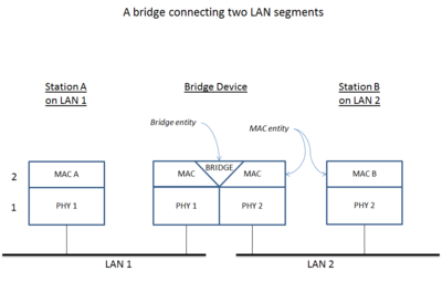
A high-level overview of network bridging, using the ISO/OSI layers and terminology
Transparent bridging
Transparent bridging uses a table called the forwarding information base to control the forwarding of frames between network segments. The table starts empty and entries are added as the bridge receives frames. If a destination address entry is not found in the table, the frame is flooded to all other ports of the bridge, flooding the frame to all segments except the one from which it was received. By means of these flooded frames, a host on the destination network will respond and a forwarding database entry will be created. Both source and destination addresses are used in this process: source addresses are recorded in entries in the table, while destination addresses are looked up in the table and matched to the proper segment to send the frame to. Digital Equipment Corporation (DEC) originally developed the technology in the 1980s.In the context of a two-port bridge, one can think of the forwarding information base as a filtering database. A bridge reads a frame's destination address and decides to either forward or filter. If the bridge determines that the destination host is on another segment on the network, it forwards the frame to that segment. If the destination address belongs to the same segment as the source address, the bridge filters the frame, preventing it from reaching the other network where it is not needed.
Transparent bridging can also operate over devices with more than two ports. As an example, consider a bridge connected to three hosts, A, B, and C. The bridge has three ports. A is connected to bridge port 1, B is connected to bridge port 2, C is connected to bridge port 3. A sends a frame addressed to B to the bridge. The bridge examines the source address of the frame and creates an address and port number entry for A in its forwarding table. The bridge examines the destination address of the frame and does not find it in its forwarding table so it floods it to all other ports: 2 and 3. The frame is received by hosts B and C. Host C examines the destination address and ignores the frame. Host B recognizes a destination address match and generates a response to A. On the return path, the bridge adds an address and port number entry for B to its forwarding table. The bridge already has A's address in its forwarding table so it forwards the response only to port 1. Host C or any other hosts on port 3 are not burdened with the response. Two-way communication is now possible between A and B without any further flooding in network.
Simple bridging
A simple bridge connects two network segments, typically by operating transparently and deciding on a frame-by-frame basis whether or not to forward from one network to the other. A store and forward technique is typically used so, during forwarding, the frame integrity is verified on the source network and CSMA/CD delays are accommodated on the destination network. In contrast to repeaters which simply extend the maximum span of a segment, bridges only forward frames that are required to cross the bridge. Additionally, bridges reduce collisions by partitioning the collision domain.Multiport bridging
A multiport bridge connects multiple networks and operates transparently to decide on a frame-by-frame basis whether and where to forward traffic. Like the simple bridge, a multiport bridge typically uses store and forward operation. The multiport bridge function serves as the basis for network switches.Implementation
The forwarding information base stored in content-addressable memory (CAM) is initially empty. For each received ethernet frame the switch learns from the frames source MAC address and adds this together with the ingress interface to build the forwarding information base. The switch then forwards the frame to the interface found in the CAM based on the frames destination MAC address. If the destination address is unknown the switch sends the frame out on all interfaces (except ingress interface). This behaviour is called unicast flooding.Forwarding
Once a bridge learns the addresses of its connected nodes, it forwards data link layer frames using a layer 2 forwarding method. There are four forwarding methods a bridge can use, of which the second through fourth methods were performance-increasing methods when used on "switch" products with the same input and output port bandwidths:- Store and forward: the switch buffers and verifies each frame before forwarding it; a frame is received in its entirety before it is forwarded.
- Cut through: the switch starts forwarding after the frame's destination address is received. There is no error checking with this method. When the outgoing port is busy at the time, the switch falls back to store-and-forward operation. Also, when the egress port is running at a faster data rate than the ingress port, store-and-forward is usually used.
- Fragment free: a method that attempts to retain the benefits of both store and forward and cut through. Fragment free checks the first 64 bytes of the frame, where addressing information is stored. According to Ethernet specifications, collisions should be detected during the first 64 bytes of the frame, so frames that are in error because of a collision will not be forwarded. This way the frame will always reach its intended destination. Error checking of the actual data in the packet is left for the end device.
- Adaptive switching: a method of automatically selecting between the other three modes .
Audio Video Bridging
Audio Video Bridging (AVB) is a common name for the set of technical standards developed by the Institute of Electrical and Electronics Engineers (IEEE) Audio Video Bridging Task Group of the IEEE 802.1 standards committee. This task group was renamed to Time-Sensitive Networking Task Group in November 2012 to reflect the expanded scope of work.The charter of this organization is to "provide the specifications that will allow time-synchronized low latency streaming services through IEEE 802 networks". These consist of:
- IEEE 802.1BA: Audio Video Bridging (AVB) Systems;
- IEEE 802.1AS: Timing and Synchronization for Time-Sensitive Applications (gPTP);
- IEEE 802.1Qat: Stream Reservation Protocol (SRP); and
- IEEE 802.1Qav: Forwarding and Queuing for Time-Sensitive Streams (FQTSS).
To help ensure interoperability between devices that implement the AVB standards, the AVnu Alliance develops device certification for the automotive, consumer, and professional audio and video markets .
Background
Audio and video (AV) equipment connections historically were analog one-way, single-purpose and point-to-point. Even digital AV standards often were point-to-point and one-way such as S/PDIF for audio and the serial digital interface (SDI) for video. This connection model resulted in large confusing masses of cables, especially in professional and high-end consumer applications.
Wiring of a patch bay of an outside broadcasting van
Benefits
Some benefits of AVB systems are:- Improved synchronization
- Low-latency
- Reliability
- No infrastructure requirements
- Networked Live Sound
Requirements
Requirements included synchronizing multiple streams to ensure they can be rendered correctly in time; a simple example of this is lip synch. For more stringent applications, such as keeping multiple digital speakers properly in phase within a professional environment, synchronization within 1μs is needed. Worst case delay, including source and destination buffering, must be low and deterministic. For example, consumer user-interface responses of about 50ms, or about 2ms for live performances. Applications must be able to reserve network resources, sometimes called admission control. AVB is also considered for industrial control applications.IEEE standardization
In July 2004, the IEEE 802.3 started a residential Ethernet study group for A/V streaming. In November 2005, work moved to the IEEE 802.1 working group, responsible for cross-network bridging standards. In particular, the group wanted the technology to be scalable from inexpensive consumer applications to professional standards.Summary of Audio Video Bridging

Figure 2 - AVB Connections
- Precise synchronization,
- Traffic shaping for media streams,
- admission controls, and
- Identification of non-participating devices.
IEEE 802.1AS - Precise synchronization
AVB devices periodically exchange timing information that allows both ends of the link to synchronize their time base reference clock very precisely. This precise synchronization has two purposes:- To allow synchronization of data streams
- To provide a common time base for sampling/receiving data streams at a source device and presenting those streams at the destination device with the same relative timing.

Figure 3 – Clocking hierarchy
The device acting as grandmaster can either be auto selected or can be specifically assigned (e.g., if the network is used in a professional environment that needs "house clock" (audio), or "genlock" (video), or if the timing hierarchy needs to be specified for other reasons). AVB devices typically exchange capability information after physical link establishment. If peer devices on a link are network synchronization capable they will start to exchange clock synchronization frames. If not, then an AVB timing domain boundary is determined (as shown in Figure 2).
IEEE 802.1Qav - Traffic shaping for AV streams
In order to provide professional AV services, the AVB architecture implements traffic shaping using existing 802.1Q forwarding and priority mechanisms but also defines a particular relationship between priority tags and frame forwarding behaviour at endpoints and bridges. Traffic shaping is the process of smoothing out the traffic for a stream, distributing its packets evenly in time. If traffic shaping is not done at sources and bridges, then the packets tend to "bunch", i.e. agglomerate, into bursts of traffic that can overwhelm the buffers in subsequent bridges, switches and other infrastructure devices. "bunching" is described in greater detail in the following sections.Tagging requirements at the stream source and the bridge
AVB streams consist of 802 frames with priority tagging and with normal restrictions on format and length. The default 802.1Q tagging for a particular market segment should be chosen to avoid potential conflict with existing uses of the 802.1Q priority tags within that market segment.Traffic shaping at the stream source
Endpoint devices are required to transmit frames very evenly for a particular stream based on the AVB traffic class and on the specific quality of service (QoS) parameters that were used when the stream was OK'd by the network (see Admission controls below). The specific rules for traffic shaping are described in the IEEE 802.1Qav specification, and are a simple form of what is known as "leaky bucket" credit-based fair queuing where the bandwidth reserved for a stream controls the time between the packets that make up the stream.
Figure 4 – Example Qav traffic shaping
Traffic shaping at an AVB bridge
The traffic shaping mechanism used by stream sources is also employed by AVB bridges. AVB frames are forwarded with precedence over Best Effort traffic (i.e., reserved AVB stream traffic traversing an AVB bridge has forwarding precedence over non-reserved traffic) and will be subjected to traffic shaping rules (they may need to wait for sufficient credits). Just like for stream sources, the traffic shaping rules for bridges require that frames be distributed very evenly in time, but only on an aggregate class basis rather than on a per-stream basis. This means that all the AVB traffic being transmitted out of a particular port is distributed evenly in time measured using the QoS parameters of that class; this is the sum of the bandwidths of all the reservations for a particular AVB class for the particular port, made by the admission control process described below. This is to achieve the effect of smoothing out the delivery times (preventing bunching of frames ) while a stream propagates through a network. The limited bunching provides the very useful benefit of placing a relatively small upper limit on the size of the AVB output buffers needed at all egress ports on a bridge, independent of the number of hops in the path. This bounded buffer size is a key attribute that enables bounded delay and eliminates network congestion for admitted AV streams in AVB networks even when non-admitted traffic does experience congestion.IEEE 802.1Qat - Admission controls
Even though the preceding mechanism can reliably deliver data with a deterministic low latency and low jitter, it will only do so if the network resources (e.g., throughput on a port, buffer space in a bridge) are available along the entire path from the talker to the listener(s). In the AVB protocols, the term 'talker' denotes a stream source while 'listener' denotes a stream destination. In this architecture, it is both the talker's and the listener's responsibility to guarantee the path is available and to reserve the resources. The process to do this is specified by the 802.1Qat "Stream Reservation Protocol" (SRP). This protocol registers a stream and reserves the resources required through the entire path taken by the stream: Talkers initiate by sending an SRP "talker advertise" message. This message includes a Stream ID composed of the MAC address of the stream source plus a talker-specific 16-bit unique ID and the MAC address of the stream destination. Additionally, the "talker advertise" message includes QoS requirements (e.g., AVB traffic class and data rate information), and accumulated worst case latency. Even though the address and QoS requirements are originated by the talker, the worst case latency is recalculated at every bridge allowing the listener to communicate this information to higher layers for media synchronization sake.
Figure 5 – Successful reservation (talker advertise)

Figure 6 – Reservation acknowledge (listener ready)
LAN-specific considerations
Although the intent of the AVB Task Group is to provide a LAN-technology-independent method for requesting and providing streaming services, the characteristics and architectures of different LAN technologies require specific ways of implementing those services as outlined in the next few sections.IEEE 802.3 / Ethernet Links
Today's Ethernet devices predominantly support full-duplex operation at 100 Mbit/s or greater. Thus, since the total available bandwidth available over such an Ethernet link is both known and constant, an AVB reservation over those Ethernet links combined with the appropriate traffic shaping assures both throughput and delivery latency parameters are met for packets of reserved streams. Since the bandwidth and delivery timing cannot be assured between two devices in an older shared CSMA/CD Ethernet using hubs, these older technologies are not supported by AVB. AVB's Ethernet time synchronization standard, 802.1AS, leverages and simplifies deployed IEEE 1588-2008.IEEE 802.11 / Wireless LAN
To date, the AVB support planned for 802.11 is limited to time synchronization. 802.1AS provides for accurate time synchronization over 802.11 links, in part by invoking MAC-specific timestamp-reporting primitives defined in IEEE Std 802.11v-2011. The time synchronization protocol defined by 802.1AS has been designed to be resilient to the transmission characteristics that are possible on wireless medium.Several MAC/PHY specifications and standards are currently deployed or being developed which operate over existing wires within the home (e.g. AC power lines, coax cabling,). These wires are electrically "Shared" between multiple devices (not point-to-point like Ethernet), so to provide predictable performance, transmission of information onto the wire is "Coordinated" to avoid collisions by one of the devices on the network. Such networking technologies are typically called Coordinated Shared Networks (CSN). If the CSN provides an access method with bounded latency (as most do), and if accurate link-specific time stamping or clock distribution is available for the CSN, then extensions can be defined to take advantage of them.
IEEE 802.1BA - Identification of participating devices
Since the whole AVB scheme depends on the participation of all devices between the talker and listener, any network element that does not support AVB (including so-called "unmanaged bridges") must be identified and flagged. The process to do this is described in the developing IEEE 802.1BA "Audio Video Bridging Systems" standard, which specifies the default configuration for AVB devices in a network. For Ethernet, the method specified by 802.1BA to determine if its peer is AVB capable is a combination of 802.3 link capabilities (determined during Ethernet link establishment) and the link delay measurements done by IEEE 802.1AS. An AVB capable Ethernet port uses AVB if:- the link is full duplex 100 Mbit/s or greater
- the 802.1AS protocol discovers exactly one peer
- the round-trip delay to the responding AVB device is no more than a worst case wire delay (computed from the IEEE 802.1AS "PDelay" exchange) Note: the worst case wire delay is less than that of a non AVB switch
- an SRP reservation request or acknowledge is received on the port
Higher layer protocols
For applications to take advantage of the features of AVB, there needs to be some coordination with portions of the higher layer communication protocols in between. In addition, some transport protocols have been adapted to provide information for applications to use AVB. An application can implement synchronized distributed rendering using 802.1AS and higher layers. Specific audio samples and/or video frames carried by higher-layer protocols are given an associated presentation time (in terms of the shared 802.1AS clock) by the media source that is also an AVB talker. Each media renderer, that is also an AVB listener, renders the referenced audio sample or video frame at the 802.1AS presentation time.IEEE 1722 and IEEE 1722.1
Applications using IEC 61883 and other formats can use procedures defined in IEEE Std 1722-2011 to sample the 802.1AS clock relevant for an A/V data block and then add the worst case transport delay to the sample time to get a presentation time which is inserted into the 1722 packet.IEEE Std 1722.1-2013 is a standard which allows AVB Discovery, Enumeration, Connection management and Control (AVDECC) of devices using IEEE Std 1722-2011.
IEEE 1733
If an application uses the IETF Real-time Transport Protocol (RTP), it can use a new RTCP payload format defined in IEEE 1733[14] that correlates the RTP timestamp with the 802.1AS presentation time. The applications at the renderer(s) then use that correlation to translate the RTP timestamp to the presentation time stamp allowing the renderer(s) to start playing at the same time and keep playing at the same rate.HTTP
Applications using HTTP can also take advantage of AVB's time synchronization by carrying a presentation time. For example, MPEG2 transport streams that require clock synchronization between the server and client can include transport time stamps (TTS) as defined by ARIB TTS (ARIB STD-B24) which are derived from the 802.1AS clock. Similarly, an application could utilize clock synchronization through methods described in ISO 13818-1 Annex J which includes a discussion of various clock recovery schemes proposed for MPEG2 Transport Streams over jitter inducing networks, and figure J.2 illustrates a simple way to use the 802.1AS clock for this purpose.If the media source is not a real-time source (e.g. a media file on a mass storage device), the presentation times can be generated based on the nominal media rate. If the media source is a real-time source (e.g. a microphone), the presentation time can be constructed by the talker based on its observation of the 802.1AS time in relation to the microphone's sample clock. Other higher layer services can use AVB in a similar way. Existing connection management schemes, for example, can use the AVB SRP reservation services by mapping their internal stream identifiers with the SRP stream ID. Once a connection is established, streaming can start. E.g., applications using RTP transmit RTCP packets defined by IEEE 1733 that correlate the SSRC to the SRP stream ID. Furthermore, listener applications using 1722 use the SRP stream ID to discriminate between different streams.
Standardization
| Standard | Title | Status | Date |
|---|---|---|---|
| IEEE 802.1BA-2011 | Audio Video Bridging Systems | Ratified and published | 30 September 2011 |
| IEEE 802.1Qav | Forwarding and Queuing Enhancements for Time-Sensitive Streams | Ratified and published | 5 January 2010 |
| IEEE 802.1Qat | Stream Reservation Protocol (SRP) | Ratified and published | 30 September 2010 |
| IEEE 802.1Q-2011 | Incorporates IEEE 802.1Qav and IEEE 802.1Qat | Ratified and published | 31 August 2011 |
| IEEE 802.1AS-2011 | Timing and Synchronization for Time-Sensitive Applications in Bridged Local Area Networks | Ratified and published | 30 March 2011 |
| IEEE 1722-2011 | Layer 2 Transport Protocol for Time Sensitive Applications in a Bridged Local Area Network | Ratified and published | 6 May 2011 |
| IEEE 1733-2011 | Layer 3 Transport Protocol for Time Sensitive Applications in Local Area Networks | Ratified and published | 25 April 2011 |
| IEEE 1722.1-2013 | Device Discovery, Enumeration, Connection Management and Control Protocol for 1722-Based Devices | Ratified and published | 23 August 2013 |
| Standard | Function Group | Title | Status | Updated Date |
|---|---|---|---|---|
| IEEE 802.1ASbt | Timing and Synchronization | Enhancements and Performance Improvements | Draft 0.7 | November 1, 2014 |
| IEEE 802.1Qbv | Forwarding and Queuing | Enhancements for Scheduled Traffic | Draft 2.1 | October 24, 2014 |
| IEEE 802.1Qbu | Forwarding and Queuing | Frame preemption | Draft 1.1 | October 16, 2014 |
| IEEE 802.1Qca | Stream Reservation (SRP) | Path Control and Reservation | Draft 1.1 | September 26, 2014 |
| IEEE 802.1CB | Stream Reservation (SRP) | Frame Replication and elimination for Reliability | Draft 0.5 | November 3, 2014 |
| IEEE 802.1Qcc | Stream Reservation (SRP) | Enhancements and Performance Improvements | Draft 0.2 | November 1, 2014 |
Networking Hardware: A Beginner’s Guide to Connected Devices

Communication Technology Bridge
The growth of the internet, bluetooth,
wifi, and GPS have demonstrated the benefits of connectivity in today’s
world. Have you ever stopped to think about the billions of tiny bits of
hardware that make this connectivity possible? Networking hardware and
infrastructure is complex and fascinating. It’s the physical receivers,
chips, a

Image source: http://ccsbmt.com/blog/networking-hardware
nd transmitters that make connectivity possible in our day to day lives.
Including cell phones, computers, smart
TVs, routers, modems, and GPSs, there are billions of devices connected
to the internet, and the number is growing daily. A new trend in
networking, the internet of things, promises to skyrocket the number of
devices on the network over the coming years as stop lights,
thermostats, security systems, and even your home refrigerator integrate
and communicate with the other devices in your life.
While the seamless automation and
efficiency of the internet of things promises to bring new levels of
productivity, it also presents challenges as it increases the load on
existing network hardware that currently powers the internet. This
article will introduce you to the basics of networking hardware and
discuss some of the challenges facing network engineers in the years to
come.
Networking Hardware: A Brief Introduction

Image source: https://fcit.usf.edu/network/chap3/chap3.htm
First Off
It wasn’t so long ago that computers
stood alone, unconnected to the internet. Dialup internet, the first
implementation of internet connection for most home users, didn’t become
widely adopted until the late-1990s. In those days, the 56 Kbps modem
was the most common network device allowing your computer to communicate
with other computers on the internet via the phone line, and if someone
in your house picked up the telephone, you’d lose your internet
connection.
Second
Since then, internet speeds have increased exponentially. According to CNN,
the average American home internet has now reached speeds over 50 Mbps.
That’s nearly 1000 times faster than internet in the 1990s. Although
the technology and means of delivery have changed dramatically, you
still need a piece of networking hardware, called a modem to receive
data from the internet and decode it into meaningful information for
your computer to use. This is the first basic piece of in-home
networking hardware: the modem that connects you to the internet.
Thirdly
In most homes, you no longer have to plug
in a cord to connect to the internet. Wifi technology comprises the
second stage of in-home networking hardware. A wireless router
communicates with your modem and broadcasts the modem’s signal to your
home. This allowing you to move freely around the house with your
wifi-enabled devices. Each of these devices – like your phone, tablet,
or laptop – has a piece of networking hardware inside of it. That little
piece of networking hardware allows it to send and receive signals from
the wireless router.
Lastly
A new trend is adding connectivity to
other devices in your home, like your thermostat or alarm system. These
connected devices that aren’t computers make up what’s known as the
internet of things, and it’s growing. However, in 2017, only about 10% of consumers
have such connected devices in their homes, so the internet of things
still remains outside of the mainstream. Over the coming years that will
change. By 2020, according to Gartner research,
there will be 25 billion devices connected to the internet of things,
not only in your home but also on the street, in stores, and everywhere
in daily life.
Low Power Solutions: Why Using and Connecting to a Bluetooth Device Makes Sense

Image source: https://www.pcworld.idg.com.au/article/624948/bluetooth-devices-could-soon-mesh-networking-capabilities/
Think About This
As the internet of things grows, it
becomes increasingly difficult for companies and consumers to manage and
power their devices. In fact, according to Network Computing,
powering devices is one of the main challenges for IoT and networking
hardware infrastructure. The sheer number of devices means that power
management and energy saving measures are going to be paramount to the
successful implementation of connected devices. Especially for companies
with large networks of devices.
Don’t Forget That
Sometimes, connecting to bluetooth device
infrastructures may make sense. Bluetooth technology has been around
for over twenty years, and it’s well-understood. It uses lower energy wavelengths
than wifi to deliver information. Most of us are familiar with
bluetooth. We may occasionally use bluetooth to pair our phones with our
car speakers or a wireless headset. However, Bluetooth has potential
for broader applications, and the low energy requirements of Bluetooth
make it an attractive alternative for connecting networking hardware.
Overall, connecting devices to the
network has huge potential to facilitate and automate everyday life. In
the near future, your fridge could tell you when you’re out of milk.
Your car will likely connect to the internet while you’re driving so it
can communicate with other cars on the road. This will offer
entertainment options for passengers. You’ll increasingly see in-store
devices at clothing retailers and grocery stores. These are items that
help you find items and give the store feedback on new things you’d like
to purchase. All these applications and more are coming in the near
future, thanks to advances in networking hardware.
XO___XO +DW DW SAW % Electronics and Communication ( e- Bridge )
The world's reliance on electronics is so great that commentators claim people live in an"electronic age." People are surrounded by electronics—televisions, radios, computers, mobiles, Laptop and DVD players, along with products with major electronic control components, such as microwave ovens, refrigerators, and other kitchen appliances, automatic vehicles, Robotics, as well as hearing aids and medical instruments and numerous applications in industry. Commonly, electronic devices contain circuitry consisting primarily or exclusively of active semiconductors supplemented with passive elements; such a circuit is described as an electronic circuit . Consumer electronics:include products like–Audio Systems, Video Systems, TV (Television),Computer, Laptop, Digital Camera, DVD Players, Home and Kitchen Appliances, GPS, Mobiles Phones etc.
Communication:Electronic communication systems connect people around the world. Using telephones, Internet and computers, people in different countries communicate almost instantly. Radios transmit sounds and televisions transmit sounds and pictures great distances. Cellular telephones enable a person to call another person. Within seconds, fax machines send and receive copies of documents over telephone lines/Satellite.
Information processing: scientists, artists, students, government and business workers, and hobbyists at home all rely on computers, Internet to handle huge amounts of information quickly and accurately. Computers solve difficult mathematical problems, maintain vast amounts of data, create complex simulations, and perform a multitude of other tasks that help people in their everyday lives.
Medicine and research: include product like X-ray machines ECG (Electrocardiogram) use radiation to take images of bones and internal organs. Radiation therapy, or radiotherapy, uses X-rays and other forms of radiation to fight cancer. Many hearing-impaired people depend on hearing aids to electrically amplify sound waves.
Computers : and other electronic instruments provide scientists and other researchers with powerful tools to better understand their area of study. Computers, for example, help scientists design new drug molecules, track weather systems, and test theories about how galaxies and stars develop . Electron microscopes use electrons rather than visible light to magnify specimens 1 million times or more.
Automation: Electronic components enable many common home appliances, such as refrigerators, washing machines, and toasters, to function smoothly and efficiently. People can electronically program coffeemakers, lawn sprinklers, and many other products to turn on and off automatically. Microwave ovens heat food quickly by penetrating it with short radio waves produced by a vacuum tube.
Instrumentation: Measuring Instruments like CRO, Multimeter, ph-meter, strain gauge, VTVM, Frequency Counter are used in different Laboratory/organizations. Many automobiles have electronic controls in their engines and fuel systems. Electronic devices also control air bags, which inflate to protect a driver and passengers in a collision .
IoT combine and conjuntion with Electronics circuits
The
Internet of Things promises convenience, marked improvements in
efficiencies, and huge economic benefits, but for such visions to be
realized the number of physical devices being integrated with the
digital world needs to continue increasing. But limiting the expansion,
and ultimate ubiquity, of this technology has been the cost, power and
size of the enabling electronics – all things that have been addressed
by a new fabrication method.
Researchers
at Purdue University and the University of Virginia are just the latest
to take on the challenge of getting physical objects connected to the
IoT cheaper and easier. To this end, they've developed a new ultra-thin
circuit fabrication method that promises to bring the IoT to pretty much
any object you can slap a label onto.
The
process behind these peelable electronic circuits not only eliminates a
number of manufacturing steps, thereby reducing cost, but it also means
almost any object can act as a sensor or be controlled via the
application of high-tech decals.
Of
course, thin-film materials are nothing new, but this wafer-recyclable,
transfer-printing process, using combinations of active nano-materials
is a step into the future, both technologically and environmentally.
Conventionally,
most electronic circuits are printed on rigid silicon wafers. These
stiff substrates need to be resilient enough to withstand the heat and
chemical etching of the process, and as such, the wafer is replaced each
time a new circuit is printed. This new technique, called "transfer
printing," allows a single wafer to be used over and over to build a
near infinite number of flexible film-based circuits, which can be
easily peeled off at room temperature by submerging the wafer and
completed circuit in water.
"It's
like the red paint on San Francisco's Golden Gate Bridge – paint peels
because the environment is very wet," says Chi Hwan Lee, Purdue
assistant professor of biomedical engineering and mechanical
engineering. "So in our case, submerging the wafer and completed circuit
in water significantly reduces the mechanical peeling stress and is
environmentally friendly."


Tidak ada komentar:
Posting Komentar