


A Technical Breakthrough in Digital Chip Tuning

RaceChip makes a decisive step in improving performance for digital signal transmission of sensor data.
From 400hp factory output in the Porsche Macan Turbo, through an additional electronic control unit, all the way to 482hp? Or from 333hp factory output in the Audi S5, with the latest generation of engines, up to 402hp? This used to be impossible due to digital signal transmission in the sensors. But RaceChip engineers have now made a decisive breakthrough. What was once reserved only for engines with analogue signal transmission of sensor data, is now also available, thanks to RaceChip, for engines with digital signal transmission. The true performance potential of an engine, combined with high-performance chip tuning and an additional control box, produce the greatest possible performance benefit. In real terms: it is now possible to add 20% more power to your engine.

The SENT-Protocol is the future of sensor-data signal transmission in vehicle engines. Volkswagen has already employed this technology in some of its more powerful Audi and Porsche variants. RaceChip is the first chip tuning manufacturer to take advantage of these signals to optimize its additional control box. We are delighted with the results so far and are confident that our customers will be just as thrilled when we complete the test phase.

RaceChip Once Again Produces Decisive, Innovative Technology
As the leading manufacturer of chip tuning products, the Göppingen-based company has succeeded in significantly optimizing engines with digital signal transmission, thanks to its highly advanced, additional control devices. RaceChip has embarked, technologically, on an entirely new journey, and with impressive initial results. The digital signal that has been specially developed for these engines allows vehicles to show their true potential. The RaceChip development team tested the Audi S5 3.0 TFSI, with a series output of 333hp, and obtained a performance increase of nearly 70hp. The tests culminated with a performance result of 402hp. In addition, the standard torque of 440Nm jumped to 483Nm. Equally impressive were the measured values of the Porsche Macan Turbo, with its 3.6 liter engine: it went from 400hp to 482hp, while the torque of 550 Nm rose to 682Nm.
As of late summer 2015, RaceChip chip tuning for vehicle engines with digital-signal transmission of sensor data will also be available to the general public. The RaceChip Ultimate comes with specifically tuned hardware and software, a 2-year engine warranty* and a 5-year product warranty. It will be available worldwide from the RaceChip online store and from RaceChip dealers. In addition to the Audi S5, the Ultimate, with this new technology, will be available for the Audi S4, A6, A7, A8, Q7 3.0 TFSI, the Porsche Macan S and Turbo and Porsche Cayenne S and GTS, in addition to the Porsche Panamera S.

About SENT
SENT is a newly developed series protocol for sensors that is to be used across the automobile industry. It stands for “Single Edge Nibble Transmission”. While old sensor technology sends an analogue value to the control box, the new sensors work digitally. They have a higher resolution, are highly reliable and are immune to electromagnetic interference - all at a low cost. Where pressure and temperature signals are received, the SENT protocol has advantages over older serial bus connections because it receives more accurate values. These can, in turn, be used at higher frequencies, allowing for very precise engine control.
Touch Technology
Introduction

Figure 1 The 'ideal' case has the field lines projecting freely into free air

Figure 2 The real life case has the sensitivity reduced by filed lines terminating to surrounding components, tracks, ground planes and the housing
The user interface of personal electronics has become critical to the success of the product. Capacitive touch sensing has become the user interface technology of choice.
Designers face challenges like electromagnetic susceptibility, parasitic capacitance, enclosure effects, variety of overlay materials and demands on low power consumption. Electrode tuning simplifies the design and improves signal to noise ratio (SNR) and reliability.
A touch controller with auto tuning maximizes sensitivity, greatly reducing the conventional constraints on PCB layout, limits to overlay thicknesses & materials and negating the need for calibration during manufacture.
The advantages of automatic tuning are:- compensation for parasitic capacitances
- higher signal-to-noise (SNR)
- large degree of freedom in PCB layout and materials due to high SNR
- adjustable sensitivity
- calibration free manufacturing
- higher EMI immunity
- lower EMI radiation
- proximity detection from the same touch electrode
The principle of capacitive sensing is based on the measurement of a disturbance introduced to the long-term steady state capacitance of the sensor. The electrode projects an electric field which is designed to be disturbed by a user touching the designated area. The capacitance of this electrode relative to the surrounding environment is continuously sampled.
Capacitive sensing sensors can achieve very high sensitivity. Due to the nature of small variations in capacitance, the sensitivity is usually very dependent on the influence of external factors. These include:
- Sources of parasitic capacitance related to the PCB layout
- Sources of parasitic capacitance related to the touch sensor housing
- Sources of external noise, including EMC disturbances and noise from the power supply
- The thickness and type of the overlay material
- Presence of air-gaps between the sensor electrode and the touch surface
Popular methods to address these influences and described in touch sensor design application notes include:
- Specific PCB routing suggestions
- Prescriptions on the power supply stability
- Suggestions for larger copper key area to improve sensitivity
- Use of hash-grounds to find an optimal point between improving immunity whilst trying not to introduce too much parasitic capacitance which reduces sensitivity in turn
- Use of active driven shields
- Limits on the thickness and type of allowable overlay materials
Whilst these methods can improve the design, they are often required to make the touch sensor system work at all. Designers will typically require multiple iterations of the touch sensor PCB layout as the design moves towards production and stability and sensitivity problems are discovered as late as pre-production, which causes costly delays.
In an age where designers are well conversed in MCU and embedded design, the design principles for sensitive and robust touch sensing remains black magic to inexperienced designers.
Using Active Parasitic Cancellation
Whilst the design guidelines will certainly improve the system sensitivity and robustness, a device which will auto tune to its environment for optimal sensitivity, will shorten design times with less PCB iterations. More importantly it will save costly delays in production where process variations, often in the mechanical construction, causes production delays due to the non-conformance of the touch sensing circuit.
From the sensor perspective, minute differences in process parameters may render the touch sensor unstable or un-usable. These include variations in the power supply stability, thickness of the overlay material, possible air gaps between sensor electrode and overlay material and in many cases, the nearness of the product’s housing. When housings are manufactured from a conductive material, the nearness of the housing introduces a large parasitic capacitance which has a significant impact on the sensor sensitivity.
Parasitic capacitance is an unwanted capacitance between sensor electrode and a nearby (normally grounded) potential. The aim of achieving a sensitive capacitive sensor is to have the sensor project electric field into a dielectric overlay material and further into free air. The user touching the designated touch sensor area would disturb this electric field.
In real life the electric field from the sensor would rather terminate to the nearby grounded potential, than be projected through a die-electric overlay and into free air. Parasitic capacitance can often account for up to 95% of the total capacitance as seen from the sensor. When 95% of the sensor capacitance is static, touching the electrode, can only impact the remaining 5% of variable capacitance. Once overlay materials exceed 1mm, the effect of the touch is as little as 5%, meaning the sensor only sees a 0.25% change between touch and non-touch. This may be very close the noise level of the system.
Figure 1 The 'ideal' case has the field lines projecting freely into free air
Figure 2 The real life case has the sensitivity reduced by filed lines terminating to surrounding components, tracks, ground planes and the housing
By using hardware compensation circuits, the effect of static parasitic capacitance could be greatly reduced. This would entail the ‘subtraction’ of the unwanted capacitance from the sensor sample, which in turn means the sensor only sees the variable capacitance, which is disturbed by the user touch. (In another analogy, this can be seen as the removal of a large DC component from a signal with a very small AC component). Once the parasitic capacitance is removed (or greatly reduced), the sensor sensitivity is recovered.
Azoteq’s range of ProxSense® capacitive touch and proximity sensors has very effective compensation circuits implemented on-chip. The on-chip implementation means that the designer does not need to worry about the design of complex analog circuits and sensitivity variation, as these are all performed on-chip.
The Azoteq technology is aptly dubbed ATI, or Automatic Tuning Implementation. The on-chip circuits will recover most of the sensor sensitivity, yielding industry leading sensitivity even in environments with severe parasitic capacitance. This further allows for the use of much thicker overlay materials, few constraints on PCB design and much greater degrees of freedom in the nearness of the product housing.
Combining the hardware cancellation with signal processing algorithms to provide auto tuning
A further advantage of an on-chip compensation implementation is that the compensation circuit can be dynamically adjusted by control algorithms. A dedicated optimization algorithm will run at power up and adjust the compensation circuit to achieve a pre-determined target. This target can be chosen to allow for maximum sensitivity, or to achieve an optimized point within a variety of parameters including:
- Sensitivity
- Power consumption
- Sampling frequency
- Noise suppression
The control algorithm will continuously monitor sensor performance and adjust the compensation circuits dynamically, should variations occur due to age, temperature, changes in the mechanical stack-up or even the addition of a static object to the touch panel area. In controllers, which are primarily designed to be used standalone, the control algorithm settings are predetermined and no intervention from a host is required. On multi channel devices, the algorithm can run autonomously. However, the host has a choice to perform partial intervention by only setting target values, or the host may take over the full control algorithm.
Advantages of parasitic cancellation and auto tune algorithms
The foremost advantage of parasitic cancellation is that sensor sensitivity is maximized, even in environments with severe parasitic capacitance. In real life cases, the reduction of parasitic capacitance is one of the biggest challenges faced by designers. With compensation circuits, the designer has much greater degrees of freedom, resulting is much smaller PCB’s and optimal performance within a product where the enclosure may add a significant parasitic capacitance.
On-chip compensation circuits allow for accurate compensation without adding to the BOM cost or PCB real estate. The on-chip circuits are calibrated during the semiconductor manufacturing and require no design skills.
Once the on-chip circuits are combined with control algorithms, the sensor may auto-tune to achieve a predetermined target. The auto-tuning algorithm will further ensure that all sensors perform similarly over manufacturing variation.
Control algorithms that allow for host intervention can be dynamically tuned to optimize the sensor. This implies that the sensor may be optimally configured for a long proximity range and low power in a standby state, whilst tuned for a high response rate in operational mode.
Experimental setup| Scenario | 1 | 2 | 3 | 4 | 5 |
| No touch, no load | Touch, no load | No touch, load added | Sensor recalibrated, no touch | Touch with load added | |
 |  |  |  | ||
| Current Sample | 937 | 433 | 309 | 856 | 587 |
| Long Term Average | 936 | 936 | 872 | 856 | 861 |
| Delta | 1 | 503 | 563 | 0 | 274 |
| Compensation | 14 | 14 | 14 | 8 | 8 |
| Multiplier | 1 | 1 | 1 | 4 | 4 |
In the table five scenarios are depicted. In scenario 3 an artificial parasitic load is added which is effectively more than an average touch. In scenario 4 an auto tune has been performed by the sensor and sensitivity is recovered, despite the large load.
Conclusion
One of the biggest challenges designers of capacitive touch solutions have to deal with is parasitic capacitance that reduces sensitivity. With a hardware compensation circuit, most of the unwanted parasitic capacitance can be removed. With such a circuit implemented on-chip, no cost is added to the BOM and the designer does not need any special skills to use the compensation circuits.
The compensation circuit can be combined with an auto-tuning algorithm that will tune the sensor to optimal performance automatically. A further benefit is that all touch sensors will have similar performance, even over variations in manufacturing.
Capacitive sensitivity is greatly increased which, allows greater degrees of freedom in PCB design, the overlay thickness and limitations on the touch sensor housing. The Azoteq implementation of on-chip compensation circuits means smaller PCB’s that function optimally in environments with severe parasitic capacitance. These controllers offer a superior touch performance and unrivalled proximity detection.
Timing Technology
Timing Technology Overview
Timers, counters, and clocks are a critical component in most embedded systems. Cell phones, computers, radios, watches, and many other devices rely for their success on an electronic oscillator that produces an output with a precise frequency to generate timing pulses and synchronize events.
Timing is a crucial aspect of digital systems, ensuring data smoothly progresses through processor pipelines and interconnected systems that can talk with each other. Many simple, low speed applications may simply rely on a microcontroller’s internal RC oscillator to provide the necessary clock signal. However, internal oscillators may be too slow and noisy for some designs, or you may need multiple devices to share a single clock. Whatever the case, there are instances where an external timing solution is necessary. In general, a designer can trade off accuracy for run time.
There are many devices that deal with timing, and some work better than others for specific applications. Devices used in timing are:
- Crystals and oscillators that oscillate or pulse with a regularity that is used to synchronize chips or functions implemented in circuits.
- Clock generators, frequency synthesizers and other integrated chips that are a more complete solution than oscillators.
- Application specific clocks or timers:
- Timing devices tuned to the exact needs of a specific technology.
- Real-time clocks or calendars that tell time in synchronization with the outside world.
- Counters.
- Accessory chips for design implementation that perform functions related to timing signals, like redrivers, buffers, dividers, jitter cleaners, counters, and so forth.
Oscillators

Simple Oscillator Circuit
Oscillators are used in timing, and are comprised of a resonator circuit and a driver circuit that detects and amplifies the resonant signal used for timing. The resonator is usually a mechanical or piezoelectric device made of crystal, ceramic, or an integrated MEMS (micro-mechanical) structure with resonating properties.
A crystal oscillator circuit is the one of the simplest external timing solutions to implement. The resonating device is built using a piezoelectric material, commonly quartz, sandwiched between two metal plates. The crystal (quartz or ceramic) translates the mechanical resonance vibration into an electrical signal at a set frequency. There are crystals that can produce pulses ranging in frequency from a few kilohertz to hundreds of megahertz. Crystals are two-terminal devices that rely on additional circuitry such as a capacitor in parallel to get the crystal to generate a set frequency. The circuitry can be located in a microcontroller chip, or the crystal can be integrated with driver circuitry into a module or chip package.
Clock Generators and Frequency Synthesizers
Many consumer applications use simple crystal-based clock generators; other applications can have very complex timing requirements with combinations of clocks for generation, synchronization, and distribution. Fortunately, timing solutions exist for almost every circuit need. These integrated circuits (ICs) reduce total component count, allow a smaller footprint, and make designing clock systems an easier task for engineers in general. The case for using timing solutions is lower cost with lower system component costs, smaller PCBs, and hopefully lower design-labor costs with a faster time-to-market.
Clock generators (or frequency generators) are used for timing circuits, synchronizing events within a system, and producing output signals at several different frequencies. Typically, the resident microcontroller (MCU) can dynamically change output frequency of the clock generator by programming it via an I2C or SPI interface.
Clock generators and frequency synthesizers are examples of timing solutions offered in integrated circuits (ICs) that, as a rule of thumb, can save cost in a system that requires four or more discrete clocks, crystals, or oscillators. The challenge is then in locating the right solution for your application. Mouser has a large selection of timing solutions, organized by function, feature, manufacturer, and/or specification.
Clock synthesizers with jitter cleaners are ICs that produce one or more clock frequencies from one input signal and also reduce phase noise and jitter. A theoretical, ideal clock source would be a pure sine wave, but in reality all clocks have some noise. Jitter is defined as deviation from a pure periodic pulsed signal, and in this context, occurs in high-frequency digital systems. Jitter attenuation is the act of reducing this deviation with specialized timing devices or circuitry. High-speed applications requiring synchronization would need jitter attenuating clock generators.
Application Specific Clocks
Most oscillators and timing circuits are general purpose, for example, most 25MHz oscillators can be used in any application that requires a 25MHz clock. However, some applications have specific timing requirements and are best served with an application-specific clock chip.
These applications often have specialized timing requirements such as managing multiple synchronous clocks, clocking a network were signal delays can be significant, or providing clock signals other than a regular frequency.
PCI Clocks
PCI and PCI Express is a very common bus interface standard that is found almost everywhere. Reliable data transfers over this interface demands a highly stable clock reference. For PCI Express the standard specifies an external reference clock, Refclk, of 100MHz with a frequency stability of ±300ppm or better. Data rates of 8GBits/sec and faster are possible.
The clock scheme for PCI bus systems is very precise. Deviations may result in bit errors, reduced throughput, or the system may fail to train, which means the clocks did not synchronize between boards on the PCI bus.
JESD204B Clocks
JESD204B defines a serial interface standard between a high speed data converter and the host processor. In these systems the data converter clock is also used to generate the clock for the JESD204B output of an ADC, or the JESD204B input of a DAC. With a data rate of up to 3.125Gbits/sec, it is important that the JESD204B clock be low jitter and also have deterministic latency.
Real-Time Clocks
A real-time clock, commonly abbreviated RTC, is an IC that provides an accurate timebase when the main power is disconnected from the system. An RTC has its own dedicated 32.768kHz oscillator and is powered by a small battery that is enabled in the absence of system power. An RTC can maintain an accurate calendar including month, day, year, and exact time down to the second. An RTC can even have a programmable alarm or count-down timer. While RTCs can be a peripheral inside the main microcontroller, a separate RTC chip can also be used.
Clock System Design
Clock buffers, redrivers, and other clock support chips are necessary when a system requires many reference frequencies to be delivered to the system. Some devices, like FPGAs, ASICs, and some digital processors, require multiple clock frequencies. If a single clock is distributed to many different destinations, it is critical that the system be designed so that the clock signal does not arrive at its destination at different times. This is called skew, or clock skew. Skew is caused by non-ideal conditions such as crosstalk, circuit board routing, and capacitive coupling, as well as circuit loads on the clock signal. It can be especially troublesome on a large network.
Jitter
Jitter is another issue in designing clock systems. Jitter is when a clock edge does not occur precisely at the ideal time, but may occur plus or minus a fraction of a second before or after the ideal edge time. Jitter can be randomly caused by unwanted electronic interference, or predictable as in deterministic jitter which is caused by known circuit physics. As long as clock jitter in a circuit is understood and minimized, it can often be compensated for in the clock system design.
Clock Buffers
Clock buffers allow a clock source to be distributed to many destinations at the proper time with little loss, adding stability to the clock distribution system. Clock buffer chips need to have a high input impedance so they will not load the clock source. Buffers must also minimize skew and jitter. Clock buffers can also be used when a delay needs to be added in order to synchronize the clock across a network.
Redrivers
Redrivers, also called repeaters, are used to improve the signal quality of high speed clocks. These devices clean up the clock signal, which includes minimizing jitter and boosting the strength of the signal.
Frequency Multipliers
Frequency multiplier/dividers are used to increase or decrease a clock signal by a multiple of its frequency. This is useful for circuits that need to generate another clock that is a multiple of the main system clock.
Clock Development Tools
Clock and timing circuit development tools can be invaluable in the design of complex clock circuits. These tools allow modifying the operating characteristics of one or more programmable clock chips. With an interface to a host PC, the developer can change on-the-fly clock system parameters while allowing easy measurement of signal characteristics like jitter and frequency.
Wireless Charging Overview
Qi (pronounced "Chee") is the global wireless charging standard developed and licensed by the largest technology alliance in the wireless charging industry, the Wireless Power Consortium (WPC). An open platform with the support of nearly 150 WPC member companies, including major mobile phone manufacturers, wireless service providers, and semiconductor companies, and with well over 300 Qi-certified products introduced into the market since the specification was first introduced in 2009, Qi is helping to bring wireless charging of mobile devices into the mainstream. Products that carry the Qi logo on their packaging are interoperable, allowing consumers the freedom to charge any Qi-compliant device, given any Qi charger.
The Qi system consists of a flat charging pad, and a mobile device equipped with a compatible receiver. When the mobile is placed on top of the charging pad, the device is charged via electromagnetic induction. Essentially, an alternating current passed through a coil in the charging pad generates a magnetic field that induces a voltage in a coil in the receiver, which can then be used to power the mobile directly or charge the battery.
Qi provides for electrical power transfer up to 4 cm (1.6 inches), with typical efficiency around 70 percent, with 80 to 85 percent efficiency possible with careful design, better shielding, and newer techniques such as the use of ultra thin coils. The low-power specification that exists today delivers up to 5 watts to receivers, enough for smart phones and small mobile gadgets.
A 10 to 15 watt extension is in the works to enable rapid phone charging and charging of consumer tablets. In development is a medium-power specification that will deliver up to 120 watts for charging larger devices such as laptop computers and power tools.
For applications requiring greater separation between the charger and receiver, such as through a desk, there is magnetic resonance technology. Though magnetic induction and magnetic resonance are both based on similar principles involving coils, AC currents, and magnetic fields, a magnetic resonance implementation offers several advantages including, 1) a range of several inches or more, 2) charging is possible through an obstruction between the charger and receiver, such as a magazine, 3) multiple devices on a charging pad can charge at the same time, and 4) flexibility in orientation and positioning of the receiving devices on the pad (Qi can achieve expanded free positioning of the receiver using a three coil transmit array). The Alliance for Wireless Power, or A4WP, champions WiPower™, the first wireless charging standard that is based on magnetic resonance. WiPower was approved in January, 2013, and devices using this standard are projected to be available in late 2014. The WPC is also working on Qi-compliant magnetic resonance technology to enable longer range charging.
Wireless power technology is still evolving, and it remains to be seen which direction the technology will go, what influences proprietary charging approaches will exert, whether standards will merge, whether manufacturers will offer multi-mode solutions that support more than one standard, and ultimately which solutions will be embraced by consumers.
XO___XO Automatic frequency control
In radio equipment, Automatic Frequency Control (AFC), also called Automatic Fine Tuning (AFT), is a method or circuit to automatically keep a resonant circuit tuned to the frequency of an incoming radio signal. It is primarily used in radio receivers to keep the receiver tuned to the frequency of the desired station.
In radio communication, AFC is needed because, after the bandpass frequency of a receiver is tuned to the frequency of a transmitter, the two frequencies may drift apart, interrupting the reception. This can be caused by a poorly controlled transmitter frequency, but the most common cause is drift of the center bandpass frequency of the receiver, due to thermal or mechanical drift in the values of the electronic components.
Assuming that a receiver is nearly tuned to the desired frequency, the AFC circuit in the receiver develops an error voltage proportional to the degree to which the receiver is mistuned. This error voltage is then fed back to the tuning circuit in such a way that the tuning error is reduced. In most frequency modulation (FM) detectors, an error voltage of this type is easily available. See Negative feedback.
AFC was mainly used in radios and television sets around the mid-20th century. In the 1970s, receivers began to be designed using frequency synthesizer circuits, which synthesized the receiver's input frequency from a crystal oscillator using the vibrations of an ultra-stable quartz crystal. These maintained sufficiently stable frequencies that AFC's were no longer needed.
Automatic SWR meter and semi-automatic tuning unit
Automatic direct reading SWR meter and Wattmeter

With supply 13.8 V, if your SWR bridge detectors output exceeds 11 volts, you will have to increase the auto SWR board supply voltage (up to 28 volts) in order to have at least about 3 volts more in supply than detectors voltage. You can also change the bridge design (with EXCEL sheet) to reduce maximum output voltages.


Second circuit, If you want to make a "Semi-auto Antenna Tuning Unit"
This is NOT A TRUE automatic antenna tuner, but this can be useful for adjustement of long wire or vertical antenna in portable operations on low bands, or for magnetic loop automatic tuning. Motor is ~ 3 rpm low voltage DC, and CV1 , air variable, with no ends of strokes.
NOTA: To use a DC motor with magnetic loop antennas, it can be necessary to reduce motor speed for precise tuning. To do this, either you decrease motor voltage (with torque loss, but generaly acceptable) , or you use a "PWM" without torque loss. PWM to be built by yourselves, or, purchased at very low cost via E-PAY, in searching "DC Motor Speed Control". Results examples: TCHONG2, or other similars , or BAKATRONICS.
NOTA: Pour utiliser le moteur sur des antennes "boucle magnétique" il peut être nécéssaire de diminuer la vitesse de rotation pour avoir un accord fin. Pour ce faire, soit vous réduisez la tension d'alimentation du moteur (avec perte de couple, mais généralement acceptable), soit vous utilisez un "PWM" sans perte de couple. PWM à réaliser par vous même, ou, à acheter pour quelques Euro, port inclus, sur E-PAY, en cherchant "DC Motor Speed Control". Exemples de résultats: TCHONG2, ou autres similaires, ou BAKATRONICS.


Semi automatic antenna tuner with PIC ( Not very useful, only if you write code yourselves )

Description de la logique de réglage


Shielding of electronic circuits is mandatory.

SWR bridge picture

Front plate & meter scale


XO ____ XO SYD Power dissipation and electronic components

An ever-present challenge in electronic circuit design is selecting suitable components that not only perform their intended task but also will survive under foreseeable operating conditions. A big part of that process is making sure that your components will stay within their safe operating limits in terms of current, voltage, and power. Of those three, the “power” portion is often the most difficult (for both newcomers and experts) because the safe operating area can depend so strongly on the particulars of the situation.
In what follows, we’ll introduce some of the basic concepts of power dissipation in electronic components, with an eye towards understanding how to select components for simple circuits with power limitations in mind.
— STARTING SIMPLE —
Let’s begin with one of the simplest circuits imaginable: A battery hooked up to a single resistor:

Here, we have a single 9 V battery, and a single 100 ? (100 Ohm) resistor, hooked up with wires to form a complete circuit.
Easy enough, right? But now a question: If you want to actually build this circuit, how “big” of a 100 ? resistor do you need to use to make sure that it doesn’t overheat? That is to say, can we just use a “regular” ¼ W resistor, like the one shown below, or do we need to go bigger?
To find out, we need to be able to calculate the amount of power that the resistor will dissipate.
Here’s the general rule for calculating power dissipation:
Here’s the general rule for calculating power dissipation:
Power Rule: P = I × VIf a current I flows through through a given element in your circuit, losing voltage V in the process, then the power dissipated by that circuit element is the product of that current and voltage: P = I × V.
Aside:
How can current times voltage end up giving us a “power” measurement?
How can current times voltage end up giving us a “power” measurement?
To understand this, we need to remember what current and voltage physically represent.
Electric current is the rate of flow of electric charge through the circuit, normally expressed in amperes, where 1 ampere = 1 coulomb per second. (The coulomb is the SI unit of electric charge.)
Voltage, or more formally, electric potential, is the potential energy per unit of electric charge —across the circuit element in question. In most cases, you can think of this as the the amount of energy that is “used up” in the element, per unit of charge that passes through. Electric potential is normally measured in volts, where 1 volt = 1 joule per coulomb. (The joule is the SI unit of energy.)
So, if we take a current times a voltage, that gives us the amount of energy that is “used up” in the element, per unit of charge, times the number of those units of charge passing through the element per second:
1 ampere × 1 volt =
1 ( coulomb / second ) × 1 ( joule / coulomb ) =
1 joule / second
1 ( coulomb / second ) × 1 ( joule / coulomb ) =
1 joule / second
The resulting quantity is in units of one joule per second: a rate of flow of energy, better known as power. The SI unit of power is the watt, where 1 watt = 1 joule per second.
Finally then, we have
1 ampere × 1 volt = 1 watt
Back to our circuit! To use the power rule (P = I × V), we need to know both the current through the resistor, and the voltage across the resistor.
First, we use Ohm’s law ( V = I × R ), to find the current through the resistor.
• The voltage across the resistor is V = 9 V.
• The resistance of the resistor is R = 100 ?.
• The voltage across the resistor is V = 9 V.
• The resistance of the resistor is R = 100 ?.
Therefore, the current through the resistor is:
I = V / R = 9 V / 100 ? = 90 mA
Then, we can use the power rule ( P = I × V ), to find the power dissipated by the resistor.
• The current through the resistor is I = 90 mA.
• The voltage across the resistor is V = 9 V.
• The current through the resistor is I = 90 mA.
• The voltage across the resistor is V = 9 V.
Therefore, the power dissipated in the resistor is:
P = I × V = 90 mA × 9 V = 0.81 W
So can you go ahead and use that 1/4 W resistor?
No, because it would likely fail from overheating.
The 100 ? resistor in this circuit needs to be rated for at least 0.81 W. Generally, one picks the next larger available size, 1 W in this case.
The 100 ? resistor in this circuit needs to be rated for at least 0.81 W. Generally, one picks the next larger available size, 1 W in this case.
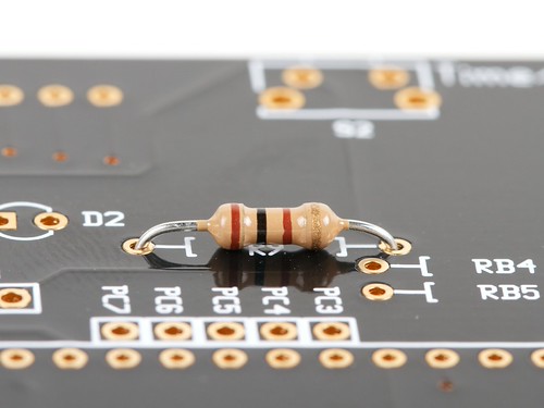
A 1 W resistor typically comes in a much larger physical package, like the one shown here:
(A 1 W, 51 ? resistor, for size comparison.)
Because a 1 W resistor is much larger physically, it should be able to handle dissipating a higher amount of power, with its higher surface area and wider leads. (It may still get very hot to the touch, but it should not get hot enough that it fails.)
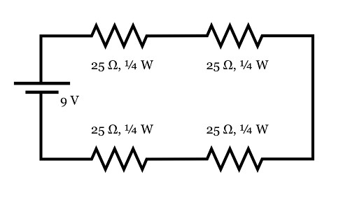
Here’s an alternate arrangement that works with four 25 ? resistors in series (which still adds up to 100 ?). In this case, the current through each resistor is still 90 mA. But, as there is only one quarter as much voltage across each resistor, there is only one quarter as much power dissipated in each resistor. For this arrangement, one only needs the four resistors to be rated for 1/4 W.
Aside: Working through that example.
Because the four resistors are in series, we can add their values together to get their total resistance, 100 ?. Using Ohm’s law with that total resistance gives us the 90 mA current again. And again, since the resistors are in series, the same current (90 mA) must flow through each, back to the battery. The voltage across each 25 ? resistor is then V = I × R, or 90 mA × 25 ? = 2.25 V. (To double check that this is reasonable, note that the voltages across the four resistors sum up to 4 × 2.25 V = 9 V.)
The power across each individual 25 ? resistor is P = I × V = 90 mA × 2.25 V ? 0.20 W, a safe level for use with a 1/4 W resistor. Intuitively, it also makes sense that if you divide up a 100 ? resistor into four equal parts, each should dissipate one quarter of the total power.
— ON BEYOND RESISTORS —
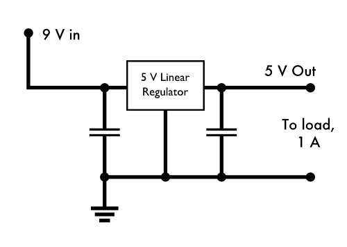
For our next example, let’s consider the following situation: Suppose that you have a circuit that takes input from a 9 V power supply, and has an onboard linear regulator to step the voltage down to 5 V, where everything actually runs. Your load, on the 5 V end, could be as high as 1 A.
What does the power look like in this situation?
The regulator essentially acts like a big variable resistor, that adjusts its resistance as needed to maintain a consistent 5 V output. When the output load is a full 1 A, the output power delivered by the regulator is 5 V × 1 A = 5 W, and the power input to the circuit by the 9 V power supply is 9 W. The voltage dropped across the regulator is 4 V, and at 1 A, that means that 4 W is dissipated by the linear regulator— also the difference between the power input and the power output.
In each part of this circuit, the power relationship is given by P = I × V. Two parts — the regulator and the load — are places where power is dissipated. And in the part of the circuit across the power supply, P = I × V describes the power input to the system— the voltage increases as the current travels across the power supply.
Additionally, it is worth noting that we have not said what kind of load is pulling that 1 A. Power is being consumed, but that does not necessarily mean that it is being converted into (just) heat energy— it could be powering a motor, or powering a set of battery chargers for example.
Aside:
While a linear voltage regulator setup like this is a very common setup for electronics, it’s worth pointing out that this is also an incredibly inefficient arrangement: 4/9 of the input power is simply burned off as heat, even when operated at lower currents.
While a linear voltage regulator setup like this is a very common setup for electronics, it’s worth pointing out that this is also an incredibly inefficient arrangement: 4/9 of the input power is simply burned off as heat, even when operated at lower currents.
— WHEN THERE ISN’T A SIMPLE “POWER” SPECIFICATION —
Next, a slightly more challenging part: making sure that your regulator can handle the power. While resistors are clearly labeled with their power capacity, linear regulators are not always. In our regulator example above, let’s further suppose that we’re using a L7805ABV regulator from ST (datasheet here).
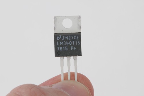
(Photo: A typical TO-220 case, the type typically used for medium-power linear regulators)
The L7805ABV is a 5 V linear regulator in a TO-220 package (similar to the one shown above), that is rated for 1.5 A output current and up to 35 V input voltage.
Naively, you might guess that you can hook this right up to 35 V input, and expect to get 1.5 A of output, meaning that the regulator would be radiating 30 V * 1.5 A = 45 W of power. But this is a tiny plastic package; it actually can’t handle that much power. If you look in the datasheet under the “Absolute maximum ratings” section, to try and find how much power it can handle, all that it says is “Internally limited” — which is anything but clear on its own.
It does turn out that there is an actual power rating, but it’s usually somewhat “hidden” within the datasheet. You can figure it out by looking at a couple of related specifications:
• TOP, Operating junction temperature range: -40 to 125 °C
• RthJA, Thermal resistance junction-ambient: 50 °C/W
• RthJC, Thermal resistance junction-case: 5 °C/W
The Operating junction temperature range, TOP, specifies how hot the “junction”– the active part of the regulator integrated circuit –can be allowed to get before it goes into thermal shutdown. (The thermal shutdown is the internal limit that makes the regulator power “Internally limited”.) For us, that’s a maximum of 125 °C.
The thermal resistance junction-ambient RthJA (Often written as ?JA), tells us how hot the junction gets when (1) the regulator is dissipating a given amount of power and (2) the regulator is sitting in open air, at a given ambient temperature. Suppose that we need to design our regulator to only work under modest commercial conditions, that will not exceed 60 °C. If we need to keep the junction temperature under 125 °C, then the maximum temperature rise that we can allow is 65°C. If we have RthJA of 50 °C/W, then the maximum power dissipation that we can allow is 65/50 = 1.3 W, if we are to prevent the regulator from going into thermal shutdown. That’s well below the 4 W that we would expect with a 1 A load current. In fact, we can only tolerate 1.3 W / 4 V = 325 mA of average output current without sending the regulator into thermal shutdown.
This, however, is for the case of the TO-220 radiating to ambient air– almost a worst-case situation. If we can add a heat sink or otherwise cool the regulator, we can do much better.
The opposite end of the spectrum is given by the other thermal specification: the thermal resistance junction-case, RthJC. This specifies how much temperature difference you can expect between the junction and the outside of the TO-220 package: only 5 °C/W. This is the relevant number if you can quickly remove heat from the package, for example if you have a very good heat sink hooked up to the outside of the TO-220 package. With a big heat sink and perfect coupling to that heat sink, at 4 W, the junction temperature would rise only 20 °C above the temperature of your heat sink. This represents the absolute minimum heating that you can expect under ideal conditions.
Depending on the engineering requirements, you can start from this point to build a full power budget, to account for the thermal conductivity of every element of your system, from the regulator itself, to the thermal interface pad between it and the heat sink, to the thermal coupling of the heat sink to the ambient air. You can then verify the couplings and relative temperatures of each component with a spot-reading non-contact infrared thermometer. But often, it’s a better choice to re-evaluate the situation and see if there’s a better way to go about this.
For the present situation, one might consider moving to a surface mount regulator that offers better power handling capability (by using the circuit board as a heat sink) or it may be worth looking into adding a power resistor (or zener diode) before the regulator to drop most of the voltage outside the regulator package, easing the load on it. Or better yet, seeing if there’s a way to build your circuit without the lossy linear regulator stage.
— AFTERWORD —
We have covered the basics of understanding power dissipation in a few simple, dc circuits.
The principles that we have gone over are quite general, and can be used to help understand power consumption in most types of passive elements and even most types of integrated circuits. There are real limitations, however, and one could spend a lifetime learning the nuances of power consumption, particularly at lower currents or high frequencies where small losses that we have neglected become important.
In ac circuits, many things behave very differently, but the power rule still holds in most circumstances: P(t) = I(t) × V(t) for time-varying current and voltage. And, not all regulators are all that lossy: Switching power supplies can convert (for example) 9 V dc to 5 V dc with 90% or higher efficiency– meaning that with good design, it may only take about 0.6 A at 9 V to produce 5 V at 1 A. But that’s a story for another time.
+++++++++++++++++++++++++++++++++++++++++++++++++++++++++++++++++++++++++++++++
e- Tuners for electronic energy
+++++++++++++++++++++++++++++++++++++++++++++++++++++++++++++++++++++++++++++++
Tidak ada komentar:
Posting Komentar