Digital electronics
Direct Gyroscope To Alignment ( DIGITAL ) electronics
 A digital signal has two or more distinguishable waveforms, in this
example, high voltage and low voltages, each of which can be mapped onto
a digit.
A digital signal has two or more distinguishable waveforms, in this
example, high voltage and low voltages, each of which can be mapped onto
a digit.
In most cases, the number of these states is two, and they are represented by two voltage bands: one near a reference value (typically termed as "ground" or zero volts), and the other a value near the supply voltage. These correspond to the false and true values of the Boolean domain respectively. Digital techniques are useful because it is easier to get an electronic device to switch into one of a number of known states than to accurately reproduce a continuous range of values.
Digital electronic circuits are usually made from large assemblies of logic gates, simple electronic representations of Boolean logic functions.
The basic logic sequence of digital is the combination of our daily life: and, or identity, not and, not or, exclusively or VIP, nor non-exclusive, as well as inner ring combinations for effective locking networks on satellite command systems using gyroscope .
X . I
Digital revolution

The Digital Revolution is a change from analog electronic and mechanical technology to digital technology that has been going on since 1980 and continues to this day. The revolution was initially probably triggered by a generation of teenagers born in the 80s. Analogous with the agricultural revolution, the Industrial revolution, the digital revolution marked the beginning of the Information age.
This digital revolution has changed the way a person views in living a very sophisticated life today. A technology that makes great changes to the whole world, from starting to help simplify all matters to the point of not being able to use this ever-sophisticated and advanced digital facility. Here is a brief history of the Digital Revolution in the development of world technology.

An example of the digital revolution of a typewriter (a bygone) into a laptop (now)
The underlying technology was discovered in 1980 and became economical to be widely adopted after the invention of Personal Computer. The technology of a previously converted digital revolution is analogous to a digital format. In digital communication for example repeating the hardware capability is able to amplify the digital signal and spread it without loss of information in the signal. Just as important as the revolution is the ability to easily move digital information between media, and to access or distribute it remotely.
An advantage of digital circuits when compared to analog circuits is that signals represented digitally can be transmitted without degradation due to noise. For example, a continuous audio signal transmitted as a sequence of 1s and 0s, can be reconstructed without error, provided the noise picked up in transmission is not enough to prevent identification of the 1s and 0s. An hour of music can be stored on a compact disc using about 6 billion binary digits.
In a digital system, a more precise representation of a signal can be obtained by using more binary digits to represent it. While this requires more digital circuits to process the signals, each digit is handled by the same kind of hardware, resulting in an easily scalable system. In an analog system, additional resolution requires fundamental improvements in the linearity and noise characteristics of each step of the signal chain.
Computer-controlled digital systems can be controlled by software, allowing new functions to be added without changing hardware. Often this can be done outside of the factory by updating the product's software. So, the product's design errors can be corrected after the product is in a customer's hands.
Information storage can be easier in digital systems than in analog ones. The noise-immunity of digital systems permits data to be stored and retrieved without degradation. In an analog system, noise from aging and wear degrade the information stored. In a digital system, as long as the total noise is below a certain level, the information can be recovered perfectly.
Even when more significant noise is present, the use of redundancy permits the recovery of the original data provided too many errors do not occur.
In some cases, digital circuits use more energy than analog circuits to accomplish the same tasks, thus producing more heat which increases the complexity of the circuits such as the inclusion of heat sinks. In portable or battery-powered systems this can limit use of digital systems.
For example, battery-powered cellular telephones often use a low-power analog front-end to amplify and tune in the radio signals from the base station. However, a base station has grid power and can use power-hungry, but very flexible software radios. Such base stations can be easily reprogrammed to process the signals used in new cellular standards.
Digital circuits are sometimes more expensive, especially in small quantities.
Most useful digital systems must translate from continuous analog signals to discrete digital signals. This causes quantization errors. Quantization error can be reduced if the system stores enough digital data to represent the signal to the desired degree of fidelity. The Nyquist-Shannon sampling theorem provides an important guideline as to how much digital data is needed to accurately portray a given analog signal.
In some systems, if a single piece of digital data is lost or misinterpreted, the meaning of large blocks of related data can completely change. Because of the cliff effect, it can be difficult for users to tell if a particular system is right on the edge of failure, or if it can tolerate much more noise before failing.
Digital fragility can be reduced by designing a digital system for robustness. For example, a parity bit or other error management method can be inserted into the signal path. These schemes help the system detect errors, and then either correct the errors, or at least ask for a new copy of the data. In a state-machine, the state transition logic can be designed to catch unused states and trigger a reset sequence or other error recovery routine.
Digital memory and transmission systems can use techniques such as error detection and correction to use additional data to correct any errors in transmission and storage.
On the other hand, some techniques used in digital systems make those systems more vulnerable to single-bit errors. These techniques are acceptable when the underlying bits are reliable enough that such errors are highly unlikely.
A single-bit error in audio data stored directly as linear pulse code modulation (such as on a CD-ROM) causes, at worst, a single click. Instead, many people use audio compression to save storage space and download time, even though a single-bit error may corrupt the entire song.
example Construction

Integrated circuits consist of multiple transistors on one silicon chip, and are the least expensive way to make large number of interconnected logic gates. Integrated circuits are usually designed by engineers using electronic design automation software (see below for more information) to perform some type of function.
Integrated circuits are usually interconnected on a printed circuit board which is a board which holds electrical components, and connects them together with copper traces.
Design
Each logic symbol is represented by a different shape. The actual set of shapes was introduced in 1984 under IEEE/ANSI standard 91-1984. "The logic symbol given under this standard are being increasingly used now and have even started appearing in the literature published by manufacturers of digital integrated circuits."Another form of digital circuit is constructed from lookup tables, (many sold as "programmable logic devices", though other kinds of PLDs exist). Lookup tables can perform the same functions as machines based on logic gates, but can be easily reprogrammed without changing the wiring. This means that a designer can often repair design errors without changing the arrangement of wires. Therefore, in small volume products, programmable logic devices are often the preferred solution. They are usually designed by engineers using electronic design automation software.
When the volumes are medium to large, and the logic can be slow, or involves complex algorithms or sequences, often a small microcontroller is programmed to make an embedded system. These are usually programmed by software engineers.
When only one digital circuit is needed, and its design is totally customized, as for a factory production line controller, the conventional solution is a programmable logic controller, or PLC. These are usually programmed by electricians, using ladder logic.
Structure of digital systems
Engineers use many methods to minimize logic functions, in order to reduce the circuit's complexity. When the complexity is less, the circuit also has fewer errors and less electronics, and is therefore less expensive.The most widely used simplification is a minimization algorithm like the Espresso heuristic logic minimizer[needs update] within a CAD system, although historically, binary decision diagrams, an automated Quine–McCluskey algorithm, truth tables, Karnaugh maps, and Boolean algebra have been used.
Representation
Representations are crucial to an engineer's design of digital circuits. Some analysis methods only work with particular representations.The classical way to represent a digital circuit is with an equivalent set of logic gates. Another way, often with the least electronics, is to construct an equivalent system of electronic switches (usually transistors). One of the easiest ways is to simply have a memory containing a truth table. The inputs are fed into the address of the memory, and the data outputs of the memory become the outputs.
For automated analysis, these representations have digital file formats that can be processed by computer programs. Most digital engineers are very careful to select computer programs ("tools") with compatible file formats.
Combinational vs. Sequential
To choose representations, engineers consider types of digital systems. Most digital systems divide into "combinational systems" and "sequential systems." A combinational system always presents the same output when given the same inputs. It is basically a representation of a set of logic functions, as already discussed.A sequential system is a combinational system with some of the outputs fed back as inputs. This makes the digital machine perform a "sequence" of operations. The simplest sequential system is probably a flip flop, a mechanism that represents a binary digit or "bit".
Sequential systems are often designed as state machines. In this way, engineers can design a system's gross behavior, and even test it in a simulation, without considering all the details of the logic functions.
Sequential systems divide into two further subcategories. "Synchronous" sequential systems change state all at once, when a "clock" signal changes state. "Asynchronous" sequential systems propagate changes whenever inputs change. Synchronous sequential systems are made of well-characterized asynchronous circuits such as flip-flops, that change only when the clock changes, and which have carefully designed timing margins.
Synchronous systems

A 4-bit ring counter using D-type flip flops is an example of
synchronous logic. Each device is connected to the clock signal, and
update together.
The state register is just a representation of a binary number. If the states in the state machine are numbered (easy to arrange), the logic function is some combinational logic that produces the number of the next state.
Asynchronous systems
As of 2014, most digital logic is synchronous because it is easier to create and verify a synchronous design. However, asynchronous logic is thought can be superior because its speed is not constrained by an arbitrary clock; instead, it runs at the maximum speed of its logic gates. Building an asynchronous system using faster parts makes the circuit faster.Nevertherless, most systems need circuits that allow external unsynchronized signals to enter synchronous logic circuits. These are inherently asynchronous in their design and must be analyzed as such. Examples of widely used asynchronous circuits include synchronizer flip-flops, switch debouncers and arbiters.
Asynchronous logic components can be hard to design because all possible states, in all possible timings must be considered. The usual method is to construct a table of the minimum and maximum time that each such state can exist, and then adjust the circuit to minimize the number of such states. Then the designer must force the circuit to periodically wait for all of its parts to enter a compatible state (this is called "self-resynchronization"). Without such careful design, it is easy to accidentally produce asynchronous logic that is "unstable," that is, real electronics will have unpredictable results because of the cumulative delays caused by small variations in the values of the electronic components.
Register transfer systems
Example of a simple circuit with a toggling output. The inverter forms
the combinational logic in this circuit, and the register holds the
state.
In register transfer logic, binary numbers are stored in groups of flip flops called registers. The outputs of each register are a bundle of wires called a "bus" that carries that number to other calculations. A calculation is simply a piece of combinational logic. Each calculation also has an output bus, and these may be connected to the inputs of several registers. Sometimes a register will have a multiplexer on its input, so that it can store a number from any one of several buses. Alternatively, the outputs of several items may be connected to a bus through buffers that can turn off the output of all of the devices except one. A sequential state machine controls when each register accepts new data from its input.
Asynchronous register-transfer systems (such as computers) have a general solution. In the 1980s, some researchers discovered that almost all synchronous register-transfer machines could be converted to asynchronous designs by using first-in-first-out synchronization logic. In this scheme, the digital machine is characterized as a set of data flows. In each step of the flow, an asynchronous "synchronization circuit" determines when the outputs of that step are valid, and presents a signal that says, "grab the data" to the stages that use that stage's inputs. It turns out that just a few relatively simple synchronization circuits are needed.
Computer design

Intel 80486DX2 microprocessor
In this way, the complex task of designing the controls of a computer is reduced to a simpler task of programming a collection of much simpler logic machines.
Almost all computers are synchronous. However, true asynchronous computers have also been designed. One example is the Aspida DLX core. Another was offered by ARM Holdings. Speed advantages have not materialized, because modern computer designs already run at the speed of their slowest component, usually memory. These do use somewhat less power because a clock distribution network is not needed. An unexpected advantage is that asynchronous computers do not produce spectrally-pure radio noise, so they are used in some mobile-phone base-station controllers. They may be more secure in cryptographic applications because their electrical and radio emissions can be more difficult to decode.
Computer architecture
Computer architecture is a specialized engineering activity that tries to arrange the registers, calculation logic, buses and other parts of the computer in the best way for some purpose. Computer architects have applied large amounts of ingenuity to computer design to reduce the cost and increase the speed and immunity to programming errors of computers. An increasingly common goal is to reduce the power used in a battery-powered computer system, such as a cell-phone. Many computer architects serve an extended apprenticeship as micro programmers.Digital circuits are made from analog components. The design must assure that the analog nature of the components doesn't dominate the desired digital behavior. Digital systems must manage noise and timing margins, parasitic inductances and capacitances, and filter power connections.
Bad designs have intermittent problems such as "glitches", vanishingly fast pulses that may trigger some logic but not others, "runt pulses" that do not reach valid "threshold" voltages, or unexpected ("undecoded") combinations of logic states.
Additionally, where clocked digital systems interface to analog systems or systems that are driven from a different clock, the digital system can be subject to metastability where a change to the input violates the set-up time for a digital input latch. This situation will self-resolve, but will take a random time, and while it persists can result in invalid signals being propagated within the digital system for a short time.
Since digital circuits are made from analog components, digital circuits calculate more slowly than low-precision analog circuits that use a similar amount of space and power. However, the digital circuit will calculate more repeatably, because of its high noise immunity. On the other hand, in the high-precision domain (for example, where 14 or more bits of precision are needed), analog circuits require much more power and area than digital equivalents.
X . II
Development of Digital Technology
Computer Development
A computer is an electronic system for manipulating data quickly and precisely and designed and organized to automatically receive and store input data, process it, and produce output under the supervision of a program instruction step and stored in the storage program memory. Data processing by using computer known as electronic data processing (PDE) or Electronic Data Processing (EDP). Data processing is the manipulation of data into a form that is more useful and more meaningful information by using an electronic device, the computer. The computer that we use today does not necessarily appear just like that but through a long process in its evolution. The matter of the emergence of computers may be seen in historical flashbacks since the use of the Abacus - found in Babylon (Iraq) some 5000 years ago - as the first manual calculation tool, both within the scope of schools and among traders, at the time. In the next period there have been many similar mechanical calculators called Pascaline discovered by Blaine Pascal in 1642, Arithometer by Charles Xavier Thomas de Colmar in 1820, Babbage's Folly by Charles Babbage in 1822, and Hollerith by Herman Hollerith in the year 1889. All of them still shaped the machine completely without electricity. The size and complexity of the structure is based on the level of operation of the calculations performed. It was not until 1940 that a new era of electrical computers began in the wake of the discovery of electric computers that employed the Boolean algebra system. In the 1980s computers became a familiar machine for the general population in the developed world, and millions of people bought computers for home use, including 17 million Commodore 64s alone between 1982 and 1994. The birth of the World Wide Web / WWW
In 1992 the World Wide Web was released to by 1996, the Internet was in the mainstream awareness and many of the business websites listed in their advertisements. In 1999, almost every country has connections, and over half of Americans use the Internet on a regular basis. In 1989, 15% of households in the United States owned computers, in 2000, this was up to 51%.
Web History begins at the European Laboratory for Particle Physics (better known as CERN), in the city of Geneva near the French and Swiss borders. CERN is an organization founded by 18 countries in Europe. In March 1989, Tim Berners Lee and other researchers from CERN proposed a protocol for information distribution systems on the Internet that enabled members spread across the world to share information and even to display the information in graphic form. The first Web Browser was created based on text. To declare a link, a line is created similar to a menu. The user typed a number to navigate within the Web. Most of the software is made for computers that use UNIX Operating System, and not much can be done by computer users at that time who have been using Windows. But all this changed after the emergence of the Mosaic browser from NCSA (National Center for Supercomputing Applications). In 1990, Berners-Lee, who was 35 years old, rethought and revived his project. This time he worked with a very sophisticated machine, NeXT computer made by Steve Jobs (founder of Apple). Incidentally, the computer has the right blend of hardware and software to display information visually. For several months, Berners-Lee rewrote his computer program and managed to create a browser, a type of internet explorer device. It also creates multiple web pages that can be accessed. This is the first version of the World Wide Web, a name coined by Berners-Lee and commonly abbreviated as WWW.Phone
Phone
Mobile phones are a common sight in western countries, with cinemas starting showing ads telling people to silence their phones. Martin Cooper is the inventor of mobile phones that use more than half the world's population. The first handset was born in 1973 with the help of Motorola team weighing two kilograms. When he suffered on the streets of New York and made his first mobile phone call from his cell phone prototype, he never imagined his device would be a success. To produce the first mobile phone, Motorola requires an equivalent of US $ 1 million. "In 1983, portable mobile phones worth US $ 4 thousand (Rp36 million) equivalent to US $ 10 thousand (Rp90 million). Cooper said his team faced the challenge of incorporating all the ingredients into a mobile phone for the first time. But eventually industrial designers have done super work and engineers completed the first two kilograms of mobile devices. "The very important ingredient for the first mobile phone is the battery weighing four or five times than the current mobile phone. Battery life time 20 minutes. After revolutionizing society in the [developed] world of the 1990s, the digital revolution spread to the masses in the developing world in the 2000s. By the end of 2005 the Internet population reached 1 billion and 3 billion people worldwide are mobile phones used by the end of the decade. Currently, television transitions from analog to digital signal Social Networking Sites
Social networking sites are a service-based web that allows users to create profiles, view available user lists, and invite or accept friends to join the site. The relationship between mobile devices and Internet web pages through "social networks" has become the standard in digital communications. The beginning of this social networking site appeared in 1997 with some sites born based on trust after the glory of social networking sites began to demand from the 2000s and 2004 appeared Friendster Friendship site continued to the next year in 2005 and so on came the site -users such as MySpace, Facebook, Twitter and others. Times are getting more sophisticated because of the technology that is always updated, everything is now easier to do. In addition to the positive impact of many negative impacts generated from social networking.Digital technology is growingThe increasingly sophisticated of today's digital technology is making huge changes to the world, the birth of a variety of advanced digital technologies has been emerging. Various circles have been facilitated in accessing information through many ways, and can enjoy the facilities of digital technology freely and in control. But in pity the growing technology is more and more crimes are detected. Therefore everything must have copyright protection and control children and teenagers in particular. So many online games that cause mental damage to children today, pornography and copyright violations were much violated.
Technology Conversion
Note Gramophone progress to CD to .mp3:
Initially, the disc is a device that has a quiver that vibrates to produce the sound of a disc, the tool needed to rotate the phonograph record is Gramophone as the technology develops, and then the disc serves to record sound or video and subsequently develops into a CD, the CD is made in Effort to streamline the music storage media by improving the sound quality produced. Then MP3, to make it easier to hear or play video / music.
VHS tape for DVD for Blu-ray:
New format for storing data in the form of video. This format is designed to meet the need for HDTV (High Definition TV) technology that promises a much sharper video quality. A single-layer Blu-ray disc can store up to 27 GB of data. This is equivalent to 2 hours of high quality (high definition) video or about 13 hours with standard video quality. As for the double layer, can accommodate up to 54 GB for about 4.5 hours of high quality video or 20 hours with standard video quality. There is even a plan to continue developing its size up to two times larger.
Analog broadcasting for digital broadcasting
Public phone to phone
E-book
Mail to email
Analog Photography to Digital Photography
Basic Information and Communication TechnologyThe underlying digital revolution is the development of digital electronic computers, which are personal computers, and in particular microprocessors with their ever-increasing performance (as described by [Moore [s law]]), which enables computer technology to be embedded into various large objects from the camera to the music player personal. Equally important is the development of transmission technologies including computer networking, Internet and digital broadcasting. 3G mobile phones, which grew rapidly in social penetration in 2000, also play a huge role in the digital revolution as they simultaneously provide ubiquitous entertainment, communication, and online connectivity. Information Technology is not just limited to computer technology (hardware and software) used to store information, but also includes communication technology to transmit information .
X . III
Automated design tools
Simple truth table-style descriptions of logic are often optimized with EDA that automatically produces reduced systems of logic gates or smaller lookup tables that still produce the desired outputs. The most common example of this kind of software is the Espresso heuristic logic minimizer.
Most practical algorithms for optimizing large logic systems use algebraic manipulations or binary decision diagrams, and there are promising experiments with genetic algorithms and annealing optimizations.
To automate costly engineering processes, some EDA can take state tables that describe state machines and automatically produce a truth table or a function table for the combinational logic of a state machine. The state table is a piece of text that lists each state, together with the conditions controlling the transitions between them and the belonging output signals.
It is common for the function tables of such computer-generated state-machines to be optimized with logic-minimization software such as Minilog.
Often, real logic systems are designed as a series of sub-projects, which are combined using a "tool flow." The tool flow is usually a "script," a simplified computer language that can invoke the software design tools in the right order.
Tool flows for large logic systems such as microprocessors can be thousands of commands long, and combine the work of hundreds of engineers.
Writing and debugging tool flows is an established engineering specialty in companies that produce digital designs. The tool flow usually terminates in a detailed computer file or set of files that describe how to physically construct the logic. Often it consists of instructions to draw the transistors and wires on an integrated circuit or a printed circuit board.
Parts of tool flows are "debugged" by verifying the outputs of simulated logic against expected inputs. The test tools take computer files with sets of inputs and outputs, and highlight discrepancies between the simulated behavior and the expected behavior.
Once the input data is believed correct, the design itself must still be verified for correctness. Some tool flows verify designs by first producing a design, and then scanning the design to produce compatible input data for the tool flow. If the scanned data matches the input data, then the tool flow has probably not introduced errors.
The functional verification data are usually called "test vectors". The functional test vectors may be preserved and used in the factory to test that newly constructed logic works correctly. However, functional test patterns don't discover common fabrication faults. Production tests are often designed by software tools called "test pattern generators". These generate test vectors by examining the structure of the logic and systematically generating tests for particular faults. This way the fault coverage can closely approach 100%, provided the design is properly made testable (see next section).
Once a design exists, and is verified and testable, it often needs to be processed to be manufacturable as well. Modern integrated circuits have features smaller than the wavelength of the light used to expose the photoresist. Manufacturability software adds interference patterns to the exposure masks to eliminate open-circuits, and enhance the masks' contrast.
Design for testability
There are several reasons for testing a logic circuit. When the circuit is first developed, it is necessary to verify that the design circuit meets the required functional and timing specifications. When multiple copies of a correctly designed circuit are being manufactured, it is essential to test each copy to ensure that the manufacturing process has not introduced any flaws.A large logic machine (say, with more than a hundred logical variables) can have an astronomical number of possible states. Obviously, in the factory, testing every state is impractical if testing each state takes a microsecond, and there are more states than the number of microseconds since the universe began. Unfortunately, this ridiculous-sounding case is typical.
Fortunately, large logic machines are almost always designed as assemblies of smaller logic machines. To save time, the smaller sub-machines are isolated by permanently installed "design for test" circuitry, and are tested independently.
One common test scheme known as "scan design" moves test bits serially (one after another) from external test equipment through one or more serial shift registers known as "scan chains". Serial scans have only one or two wires to carry the data, and minimize the physical size and expense of the infrequently used test logic.
After all the test data bits are in place, the design is reconfigured to be in "normal mode" and one or more clock pulses are applied, to test for faults (e.g. stuck-at low or stuck-at high) and capture the test result into flip-flops and/or latches in the scan shift register(s). Finally, the result of the test is shifted out to the block boundary and compared against the predicted "good machine" result.
In a board-test environment, serial to parallel testing has been formalized with a standard called "JTAG" (named after the "Joint Test Action Group" that proposed it).
Another common testing scheme provides a test mode that forces some part of the logic machine to enter a "test cycle." The test cycle usually exercises large independent parts of the machine.
Trade-offs
Several numbers determine the practicality of a system of digital logic: cost, reliability, fanout and speed. Engineers explored numerous electronic devices to get an ideal combination of these traits.Cost
The cost of a logic gate is crucial, primarily because very many gates are needed to build a computer or other advanced digital system and because the more gates can be used, the more capable and/or fast the machine can be. Since the majority of a digital computer is simply an interconnected network of logic gates, the overall cost of building a computer correlates strongly with the price per logic gate. In the 1930s, the earliest digital logic systems were constructed from telephone relays because these were inexpensive and relatively reliable. After that, engineers always used the cheapest available electronic switches that could still fulfill the requirements.The earliest integrated circuits were a happy accident. They were constructed not to save money, but to save weight, and permit the Apollo Guidance Computer to control an inertial guidance system for a spacecraft. The first integrated circuit logic gates cost nearly $50 (in 1960 dollars, when an engineer earned $10,000/year). To everyone's surprise, by the time the circuits were mass-produced, they had become the least-expensive method of constructing digital logic. Improvements in this technology have driven all subsequent improvements in cost.
With the rise of integrated circuits, reducing the absolute number of chips used represented another way to save costs. The goal of a designer is not just to make the simplest circuit, but to keep the component count down. Sometimes this results in more complicated designs with respect to the underlying digital logic but nevertheless reduces the number of components, board size, and even power consumption. A major motive for reducing component count on printed circuit boards is to reduce the manufacturing defect rate and increase reliability, as every soldered connection is a potentially bad one, so the defect and failure rates tend to increase along with the total number of component pins.
For example, in some logic families, NAND gates are the simplest digital gate to build. All other logical operations can be implemented by NAND gates. If a circuit already required a single NAND gate, and a single chip normally carried four NAND gates, then the remaining gates could be used to implement other logical operations like logical and. This could eliminate the need for a separate chip containing those different types of gates.
Reliability
The "reliability" of a logic gate describes its mean time between failure (MTBF). Digital machines often have millions of logic gates. Also, most digital machines are "optimized" to reduce their cost. The result is that often, the failure of a single logic gate will cause a digital machine to stop working. It is possible to design machines to be more reliable by using redundant logic which will not malfunction as a result of the failure of any single gate (or even any two, three, or four gates), but this necessarily entails using more components, which raises the financial cost and also usually increases the weight of the machine and may increase the power it consumes.Digital machines first became useful when the MTBF for a switch got above a few hundred hours. Even so, many of these machines had complex, well-rehearsed repair procedures, and would be nonfunctional for hours because a tube burned-out, or a moth got stuck in a relay. Modern transistorized integrated circuit logic gates have MTBFs greater than 82 billion hours (8.2 · 1010 hours), and need them because they have so many logic gates.
Fanout
Fanout describes how many logic inputs can be controlled by a single logic output without exceeding the electrical current ratings of the gate outputs. The minimum practical fanout is about five. Modern electronic logic gates using CMOS transistors for switches have fanouts near fifty, and can sometimes go much higher.Speed
The "switching speed" describes how many times per second an inverter (an electronic representation of a "logical not" function) can change from true to false and back. Faster logic can accomplish more operations in less time. Digital logic first became useful when switching speeds got above 50 Hz, because that was faster than a team of humans operating mechanical calculators. Modern electronic digital logic routinely switches at 5 GHz (5 · 109 Hz), and some laboratory systems switch at more than 1 THz (1 · 1012 Hz).Logic families
Design started with relays. Relay logic was relatively inexpensive and reliable, but slow. Occasionally a mechanical failure would occur. Fanouts were typically about 10, limited by the resistance of the coils and arcing on the contacts from high voltages.Later, vacuum tubes were used. These were very fast, but generated heat, and were unreliable because the filaments would burn out. Fanouts were typically 5...7, limited by the heating from the tubes' current. In the 1950s, special "computer tubes" were developed with filaments that omitted volatile elements like silicon. These ran for hundreds of thousands of hours.
The first semiconductor logic family was resistor–transistor logic. This was a thousand times more reliable than tubes, ran cooler, and used less power, but had a very low fan-in of 3. Diode–transistor logic improved the fanout up to about 7, and reduced the power. Some DTL designs used two power-supplies with alternating layers of NPN and PNP transistors to increase the fanout.
Transistor–transistor logic (TTL) was a great improvement over these. In early devices, fanout improved to 10, and later variations reliably achieved 20. TTL was also fast, with some variations achieving switching times as low as 20 ns. TTL is still used in some designs.
Emitter coupled logic is very fast but uses a lot of power. It was extensively used for high-performance computers made up of many medium-scale components (such as the Illiac IV).
By far, the most common digital integrated circuits built today use CMOS logic, which is fast, offers high circuit density and low-power per gate. This is used even in large, fast computers, such as the IBM System z.
Recent developments
In 2009, researchers discovered that memristors can implement a boolean state storage (similar to a flip flop, implication and logical inversion), providing a complete logic family with very small amounts of space and power, using familiar CMOS semiconductor processes.The discovery of superconductivity has enabled the development of rapid single flux quantum (RSFQ) circuit technology, which uses Josephson junctions instead of transistors. Most recently, attempts are being made to construct purely optical computing systems capable of processing digital information using nonlinear optical elements.
X . IIII
Ringing (signal) for process ROBO
It is also known as ripple, particularly in electricity or in frequency domain response.

An illustration of overshoot, followed by ringing and settle time.
Electricity
In electrical circuits, ringing is an unwanted oscillation of a voltage or current. It happens when an electrical pulse causes the parasitic capacitances and inductances in the circuit (i.e. those that are not part of the design, but just by-products of the materials used to construct the circuit) to resonate at their characteristic frequency. Ringing artifacts are also present in square waves; see Gibbs phenomenon.Ringing is undesirable because it causes extra current to flow, thereby wasting energy and causing extra heating of the components; it can cause unwanted electromagnetic radiation to be emitted ; it can delay arrival at a desired final state (increase settling time); and it may cause unwanted triggering of bistable elements in digital circuits. Ringy communications circuits may suffer falsing.
Ringing can be due to signal reflection, in which case it may be minimized by impedance matching.
Video
In video circuits, electrical ringing causes closely spaced repeated ghosts of a vertical or diagonal edge where dark changes to light or vice versa, going from left to right. In a CRT the electron beam upon changing from dark to light or vice versa instead of changing quickly to the desired intensity and staying there, overshoots and undershoots a few times. This bouncing could occur anywhere in the electronics or cabling and is often caused by or accentuated by a too high setting of the sharpness control.Audio
Ringing can affect audio equipment in a number of ways. Audio amplifiers can produce ringing depending on their design, although the transients that can produce such ringing rarely occur in audio signals.Transducers (i.e., microphones and loudspeakers) can also ring. Mechanical ringing is more of a problem with loudspeakers as the moving masses are larger and less easily damped, but unless extreme they are difficult to audibly identify.
In digital audio, ringing can occur as a result of filters such as brickwall filters. Here, the ringing occurs before the transient as well as after.
Signal processing
In signal processing, "ringing" may refer to ringing artifacts: spurious signals near sharp transitions. These have a number of causes, and occur for instance in JPEG compression and as pre-echo in some audio compression.X . IIIII
DIGITAL GYROSCOPE
Gyro sensors - How they work and what's ahead
Gyro sensors
Gyro sensors, also known as angular rate sensors or angular velocity sensors, are devices that sense angular velocity.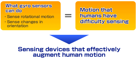
| Angular velocity |
|---|
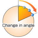 In simple terms, angular velocity is the change in rotational angle per unit of time. Angular velocity is generally expressed in deg/s (degrees per second). |
Gyro Sensor Types
Gyro sensors come in a variety of types. Here, different types are plotted by size and performance.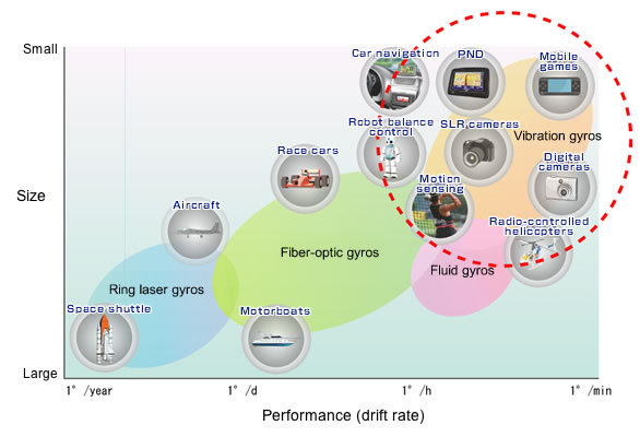

Moving forward, demand
for vibration gyros is expected to grow in areas such as vehicle driver
safety and support systems, and in robot motion control.
Vibration Gyro Sensors
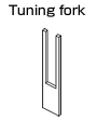
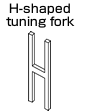
Vibration gyro sensors sense angular velocity from the Coriolis force applied to a vibrating element. For this reason, the accuracy with which angular velocity is measured differs significantly depending on element material and structural differences. Here, we briefly describe the main types of elements used in vibration gyro sensors.Types of elements used in vibration gyro sensors
Vibration gyro sensor manufacturers are using a variety of materials and structures in an effort to devise compact, high-accuracy gyro sensors that have good characteristics, including:• scale factor
• temperature-frequency coefficient
• compact size
• shock resistance
• stability
• noise characteristics
• noise characteristics
| Material | Sample Structure | |
|---|---|---|
| Piezoelectric transducer |  |
   |
| Ceramic |   |
|
| Silicon transducer | Silicon | Si MEMS NOTE: Every company uses a different structure. |
How Angular Velocity Sensing Works (in Vibration Gyro Sensors)
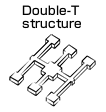
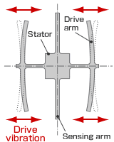
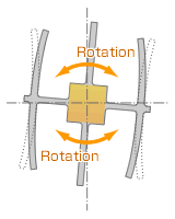
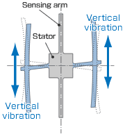
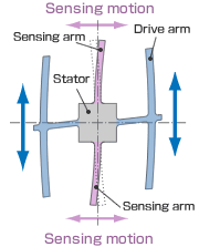
Vibration gyro sensors sense angular velocity from the Coriolis force applied to a vibrating object.Here, we explain how this works, using as an example Epson 's double-T structure crystal element.
| Vibration gyro sensors sense angular velocity from the Coriolis force applied to a vibrating object. Here, we explain how this works, using as an example Epson 's double-T structure crystal element.
Gyro Sensor ApplicationsThere are three main applications for gyro sensors.

Interesting facts
Examples of angular velocity in applications: • Car navigation systems: ~10 deg/s • Vehicle control: ~30 deg/s • Camera-shake correction: ~100 deg/s • Game controllers: ~300 deg/s • Sensing the swing of golf's top players: ~3,000 deg/s Sample applications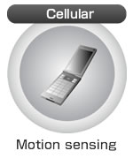   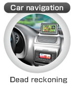 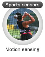 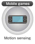 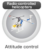  
Gyro sensors are used in products all around us.
|
|||||||||||||||||||||||||||||||||||||||||
Gyroscope
For other uses and non-rotary gyroscopes,

A gyroscope

A gyroscope in operation. Note the freedom of rotation in all three
axes. The rotor will maintain its spin axis direction regardless of the
orientation of the outer frame.
Gyroscopes based on other operating principles also exist, such as the electronic, microchip-packaged MEMS gyroscopes found in consumer electronics devices, solid-state ring lasers, fibre optic gyroscopes, and the extremely sensitive quantum gyroscope. Applications of gyroscopes include inertial navigation systems where magnetic compasses would not work, as in the Hubble telescope, or inside the steel hull of a submerged submarine, or would not be precise enough. Due to their precision, gyroscopes are also used in gyrotheodolites to maintain direction in tunnel mining. Gyroscopes can be used to construct gyrocompasses, which complement or replace magnetic compasses (in ships, aircraft and spacecraft, vehicles in general), to assist in stability (Hubble Space Telescope, bicycles, motorcycles, and ships) or be used as part of an inertial guidance system. Description and diagram
Diagram of a gyro wheel. Reaction arrows about the output axis (blue)
correspond to forces applied about the input axis (green), and vice
versa.
The axle of the spinning wheel defines the spin axis. The rotor is constrained to spin about an axis, which is always perpendicular to the axis of the inner gimbal. So the rotor possesses three degrees of rotational freedom and its axis possesses two. The wheel responds to a force applied to the input axis by a reaction force to the output axis. The behaviour of a gyroscope can be most easily appreciated by consideration of the front wheel of a bicycle. If the wheel is leaned away from the vertical so that the top of the wheel moves to the left, the forward rim of the wheel also turns to the left. In other words, rotation on one axis of the turning wheel produces rotation of the third axis. A gyroscope flywheel will roll or resist about the output axis depending upon whether the output gimbals are of a free or fixed configuration. Examples of some free-output-gimbal devices would be the attitude reference gyroscopes used to sense or measure the pitch, roll and yaw attitude angles in a spacecraft or aircraft. 
Animation of a gyro wheel in action
In some special cases, the outer gimbal (or its equivalent) may be omitted so that the rotor has only two degrees of freedom. In other cases, the centre of gravity of the rotor may be offset from the axis of oscillation, and, thus, the centre of gravity of the rotor and the centre of suspension of the rotor may not coincide. Contemporary usesSteadicamA Steadicam rig was employed during the filming of Return of the Jedi, in conjunction with two gyroscopes for extra stabilization, to film the background plates for the speeder bike chase. Steadicam inventor Garrett Brown operated the shot, walking through a redwood forest, running the camera at one frame per second. When projected at 24 frames per second, it gave the impression of flying through the air at perilous speeds.Heading indicatorThe heading indicator or directional gyro has an axis of rotation that is set horizontally, pointing north. Unlike a magnetic compass, it doesn't seek north. When being used in an airliner, for example, it will slowly drift away from north, and will need to be reoriented periodically, using a magnetic compass as a reference.GyrocompassUnlike a directional gyro or heading indicator, a gyrocompass seeks north. It detects the rotation of the Earth about its axis and seeks the true north, rather than the magnetic north. Gyrocompasses usually have inbuilt damping to prevent overshoot when recalibrating due to sudden movement.AccelerometerAnother problem to be solved is to determine where one is. By determining one's acceleration and integrating over time, one can determine one's velocity. Integrating again, one can find one's position. The simplest accelerometer, conceptually, is a weight that is free to move horizontally, attached to a spring and a device to measure the tension in the spring. This can be improved by introducing a counteracting force to push the weight back and to measure the force needed to prevent the weight from moving. A more complicated design consists of a gyroscope with a weight on one of the axes. The device will react to the force generated by the weight when it is accelerated, by integrating that force to produce a velocity. Thus only one more integration is needed to obtain one's position.VariationsGyrostatA gyrostat is a variant of the gyroscope. It consists of a massive flywheel concealed in a solid casing. Its behaviour on a table, or with various modes of suspension or support, serves to illustrate the curious reversal of the ordinary laws of static equilibrium due to the gyrostatic behaviour of the interior invisible flywheel when rotated rapidly. The first gyrostat was designed by Lord Kelvin to illustrate the more complicated state of motion of a spinning body when free to wander about on a horizontal plane, like a top spun on the pavement, or a hoop or bicycle on the road. Kelvin also made use of gyrostats to develop mechanical theories of the elasticity of matter and of the ether; these theories are of purely historical interest today.In modern times, the gyrostat concept is used in the design of attitude control systems for orbiting spacecraft and satellites. For instance, the Mir space station had three pairs of internally mounted flywheels known as gyrodynes or control moment gyros. In physics, there are several systems whose dynamical equations resemble the equations of motion of a gyrostat. Examples include a solid body with a cavity filled with an inviscid, incompressible, homogeneous liquid, the static equilibrium configuration of a stressed elastic rod in elastica theory, the polarization dynamics of a light pulse propagating through a nonlinear medium, the Lorenz system in chaos theory, and the motion of an ion in a Penning trap mass spectrometer. MEMSA MEMS gyroscope takes the idea of the Foucault pendulum and uses a vibrating element, known as a MEMS (microelectromechanical system). The MEMS-based gyro was initially made practical and producible by Systron Donner Inertial (SDI). Today, SDI is a large manufacturer of MEMS gyroscopes.HRGThe hemispherical resonator gyroscope (HRG), also called wine-glass gyroscope or mushroom gyro, makes using a thin solid-state hemispherical shell, anchored by a thick stem. This shell is driven to a flexural resonance by electrostatic forces generated by electrodes which are deposited directly onto separate fused-quartz structures that surround the shell. Gyroscopic effect is obtained from the inertial property of the flexural standing waves.VSG or CVGA vibrating structure gyroscope (VSG), also called a Coriolis vibratory gyroscope (CVG), uses a resonator made of different metallic alloys. It takes a position between the low-accuracy, low-cost MEMS gyroscope and the higher-accuracy and higher-cost FOG. Accuracy parameters are increased by using low-intrinsic damping materials, resonator vacuumization, and digital electronics to reduce temperature dependent drift and instability of control signals.High quality wine-glass resonators are used for precise sensors like HRG or CRG. DTGA dynamically tuned gyroscope (DTG) is a rotor suspended by a universal joint with flexure pivots. The flexure spring stiffness is independent of spin rate. However, the dynamic inertia (from the gyroscopic reaction effect) from the gimbal provides negative spring stiffness proportional to the square of the spin speed (Howe and Savet, 1964; Lawrence, 1998). Therefore, at a particular speed, called the tuning speed, the two moments cancel each other, freeing the rotor from torque, a necessary condition for an ideal gyroscope.Ring laser gyroscopeA ring laser gyroscope relies on the Sagnac effect to measure rotation by measuring the shifting interference pattern of a beam split into two halves, as the two halves move around the ring in opposite directions.When the Boeing 757-200 entered service in 1983, it was equipped with the first suitable ring laser gyroscope. This gyroscope took many years to develop, and the experimental models went through many changes before it was deemed ready for production by the engineers and managers of Honeywell and Boeing. It was an outcome of the competition with mechanical gyroscopes, which kept improving. The reason Honeywell, of all companies, chose to develop the laser gyro was that they were the only one that didn't have a successful line of mechanical gyroscopes, so they wouldn't be competing against themselves. The first problem they had to solve was that with laser gyros rotations below a certain minimum could not be detected at all, due to a problem called "lock-in", whereby the two beams act like coupled oscillators and pull each other's frequencies toward convergence and therefore zero output. The solution was to shake the gyro rapidly so that it never settled into lock-in. Paradoxically, too regular of a dithering motion produced an accumulation of short periods of lock-in when the device was at rest at the extremities of its shaking motion. This was cured by applying a random white noise to the vibration. The material of the block was also changed from quartz to a new glass ceramic Cer-Vit, made by Owens Corning, because of helium leaks. Fiber optic gyroscopeA fiber optic gyroscope also uses the interference of light to detect mechanical rotation. The two halves of the split beam travel in opposite directions in a coil of fiber optic cable as long as 5 km. Like the ring laser gyroscope, it makes use of the Sagnac effect.London momentA London moment gyroscope relies on the quantum-mechanical phenomenon, whereby a spinning superconductor generates a magnetic field whose axis lines up exactly with the spin axis of the gyroscopic rotor. A magnetometer determines the orientation of the generated field, which is interpolated to determine the axis of rotation. Gyroscopes of this type can be extremely accurate and stable. For example, those used in the Gravity Probe B experiment measured changes in gyroscope spin axis orientation to better than 0.5 milliarcseconds (1.4×10⁻⁷ degrees) over a one-year period. This is equivalent to an angular separation the width of a human hair viewed from 32 kilometers (20 mi) away.The GP-B gyro consists of a nearly-perfect spherical rotating mass made of fused quartz, which provides a dielectric support for a thin layer of niobium superconducting material. To eliminate friction found in conventional bearings, the rotor assembly is centered by the electric field from six electrodes. After the initial spin-up by a jet of helium which brings the rotor to 4,000 RPM, the polished gyroscope housing is evacuated to an ultra-high vacuum to further reduce drag on the rotor. Provided the suspension electronics remain powered, the extreme rotational symmetry, lack of friction, and low drag will allow the angular momentum of the rotor to keep it spinning for about 15,000 years. A sensitive DC SQUID that can discriminate changes as small as one quantum, or about 2 ×10⁻¹⁵ Wb, is used to monitor the gyroscope. A precession, or tilt, in the orientation of the rotor causes the London moment magnetic field to shift relative to the housing. The moving field passes through a superconducting pickup loop fixed to the housing, inducing a small electric current. The current produces a voltage across a shunt resistance, which is resolved to spherical coordinates by a microprocessor. The system is designed to minimize Lorentz torque on the rotor. Consumer electronics
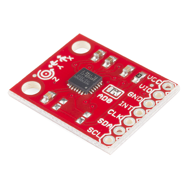
A digital gyroscope module connected to an Arduino Uno board
Nintendo has integrated a gyroscope into the Wii console's Wii Remote controller by an additional piece of hardware called "Wii MotionPlus". It is also included in the 3DS and the Wii U GamePad, which detects movement when turning. Cruise ships use gyroscopes to level motion-sensitive devices such as self-leveling pool tables. An electric powered flywheel gyroscope inserted in a bicycle wheel is being sold as a training wheel alternative. | |||||||||||||||||||||||||||||||||||||||||
  X . IIIIIIComplete Introduction in Establishing Augmentation & Communication Process Through Artificial Nano Implant Digital Circuit InterfaceWith Quantum mechanics at play, Nano Particles serve as perfect interface between the physical and the digital worlds. These Nano Implants can be then hardwired directly into human brain or nerve cells, hence forth making the time lag negligible. With advancement in laser surgery, it’s plausible to think of nano surgeries. Furthermore, with instructions hard coded into the nano implants, these nano augmentations can ease up significant number of human needs. A brain augmented person, for example, can have perfect memory retentive capacity, the ability to share information on the fly and the ability to process the physical world in cybernetic conception. Information exchange would increase significantly, as all people would be connected in the digital world. Concluding, we can say that even with the sheer risks involved, the endless possibilities poised by Nano Augmentation as an interface cant be ignored. It would completely change the standard of living, with the profound information exchange making the global village even smaller. Mr YES and Clark was perhaps very right in these words. We live in a world where magic exists, thanks to the ongoing technological revolution. One such technological innovation lies in perhaps two of the most happening branches of Science, The Nanotechnology and the Augmentation Technology. Augmentation here has broad meaning, but processing the word in the scientific sense, it means modulating the Physical world with which we interact and moulding it with cyber interface. Speaking more specifically, augmenting means connecting the physical world and the digital world real time. Augmentation is generally achieved by Interfaces, such as head mounted displays, to connect the digital world and the physical world. Nanotechnology is defined as the study of manipulating matter on an atomic and molecular scale (on the size of 1 to 100 nm). Broader sense again, we can actually manufacture hardwares the size of nanometers by manipulation of atoms and electrons. With Quantum mechanics at play, the implications of Nano Tech is huge. We can create new atomic level materials that can have effect on every conceivable genre of Science and Technology, especially medicines. But perhaps the most exciting aspect about nano technology is that it can help us bridge the gap between biology and hardware, as nano hardware can easily act as implants due to it’s sheer small size. Hence forth, we can define Nano Augmentation as those nano hardwares or implants that can allow us to perceive the digital world in an augmented format. It allows us to conceive the cyber reality in real time and be digitally connected 24X7. Nano Implants blurs the boundaries between the physical and the digital world. It replaces the traditional existing interface, for example Ipad or 3D display, that is generally used for creating the cyber reality .  lthough several attempts have been made to bridge the gap between the physical world and the digital world, it’s the interface which has always poised a problem. The existing interface has numerous problems that warrant a potential shift to nano implants.
The Idea: Nano Augmentation
Redefining the Nano Augmentation word,
they are the nano implants that replace the existing problematic
interface, and serve as the new upgraded interface with many added
functionalities. Using the concept of Nano Biology, they can also act as
cell replacements in the near future.
A Nano implant is generally manufactured
from inorganic materials such as silicon or germanium with the help of
nano technology. They consist of Power supply, Communicator
module, Chemical synthesizers, Nucleus probe with sensors and mechanical
effectors and a virus detector/eliminator. The functionality of the implants are hard coded into them.
These nano implants are then surgically
placed into the required body parts. The bottom line here lies in
establishing a clear communication link between human nerves and the
implant’s communicator module. These communications are enhanced usingpartially invasive Brain Computer Interface (BCI) methods
or Biosensors. Partially invasive BCI means that the implants are not
inserted into the brain or the said body part, instead, the implants are
just glazed into the surface of the brain or the said body part. Hence
forth, it is necessary that the implant must depict an almost artificial
neuron behavior, as for real time communication process it is mandatory
to instigate an artificial immune & communication system. That’s
because it’s our body’s immune system that acts as an interface between
the human thought process and the neurons. We seek to inject this
natural interface with our artificial one, so as to grasp the human
thought process and transform it into digital commands via Nano
Implants. Hence forth, the nano implants, at it’s basic, must depict
artificial neuron behavior as far as possible.
The communication process of body and
hardware would happen between the tendrils of human neurons and the
implants, much like the neurons interact with other cells. Nerve signals
generated by action potentials and electrical energies generated by brain cortex,
or specific area of brains would be detected by Bio sensors, and then
transferred to the Communication module inside the nano implants for
feedback. The implants would generate a similar target signal to
interact with the human body. Broadly speaking again, a similiar kind of
interface would be formed between human thought and artificial
implants, much as the interface that is formed between human thought and
neurons.
Once the implants are in place, they are
activated to connect digitally with the cyber world. Here, the
communication process with the global net happens with the help ofWi-Fi,
or more specifically, Radio Waves. Hence, a proper interface is
established between the cyber world, the physical world and the human
body.
Communication Process: Given
above is communication process that happens between Nano Implant and
the VR application. The connected implant picks up the EM signatures or
signals generated from the brain cortex or target dendrite. These
electrical signals are then digitized, processed in real time,
translated to the application signal and then finally, the signal
commands are transferred to the said VR application via Wi-Fi in the
form of Radio waves. The reverse happens in case we want a feedback from
the VR application. The received Wi-Fi or radio wave signal is
converted into the electrical form, and then fired back into the
neurotic network or the targetted dendrite via Implant’s Communication
Module. Henceforth, a two way connecton is established almost
seamlessly. Given
above is communication process that happens between Nano Implant and
the VR application. The connected implant picks up the EM signatures or
signals generated from the brain cortex or target dendrite. These
electrical signals are then digitized, processed in real time,
translated to the application signal and then finally, the signal
commands are transferred to the said VR application via Wi-Fi in the
form of Radio waves. The reverse happens in case we want a feedback from
the VR application. The received Wi-Fi or radio wave signal is
converted into the electrical form, and then fired back into the
neurotic network or the targetted dendrite via Implant’s Communication
Module. Henceforth, a two way connecton is established almost
seamlessly.
Given above is the core circuit design for the nano Implant. The above pic is the nobel prize winning Hodgkin–Huxley model
which accurately depicts the action potential of a neuron. Basically,
it is a set of nonlinear ordinary differential equations that
approximates the electrical characteristics of excitable cells such as
neurons and cardiac myocytes. The lipid bilayer is represented as a capacitance (Cm). Voltage-gated and leak ion channels are represented by nonlinear (gn) and linear (gL) conductances, respectively. The electrochemical gradients driving the flow of ions are represented bybatteries (E), and ion pumps and exchangers are represented by current sources (Ip).
We can use this model as the core circuitary for the nano implants. The
simplfied equations in the FitzHugh-Nagumo model would further ease the
process of creating the digital nano circuit. Bottom line,
Hodgkin-Huxley model acts as the partial blueprint towards creation of
artificial neuron circuits in the form of nano implants. The equation
would read as:
The existing Hodgkin-Huxley model has been
extended a lot since it’s inception, but we must note that at it’s
core, the model would serve it’s purpose. What is meant is that by
expanding and extending the Hodgin-Huxley model, we can create or
recreate a suitable Nano Implant digital model. Most notable in this
regard is the Cable Theory model, where the existing
model is depicted as as a cylindrical structure undergoing a regular
pattern of bifurcation, with total output conductance given as:

Henceforth, creating the digital circuitry wont be much of a hassle.
Now we discuss the equations once the
artificial implants are in place with the natural neuron circuit. For a
given artificial neuron, let there be m + 1 inputs with signals x0through xm and weights w0 through wm. Usually, the x0 input is assigned the value +1, which makes it a bias input with wk0 = bk. This leaves only m actual inputs to the neuron: from x1 to xm. The output of kth neuron is:
 Where Where  (phi) is the transfer function. (phi) is the transfer function.
Furthermore:

Hence we can see, the output behavior is
analogous to a natural axon circuit of a human neuron. Its value
propagates to input of the next layer, through a synapse. It may also
exit the system, possibly as part of an output vector. Broadly speaking,
the output of the kth neuron, in this case our artificial implant,
would be analogous to the output of the kth natural neuron in the
complicated dendrite circuit. Henceforth, we would take inputs from
several targetted dendrites, and calculate the output of the artificial
implant using the given equation, faciliating our knowledge of the
output voltage generated in the Hodgin-Huxley model or the reimagined
Nano Implant digital circuit.

The above pic approximately denotes the
nano electrode which we would use for the partially invasive BCI
process. As explained before, we wont be fitting the implants directly
into human brain, as that would prove to be very dangerous to the brain
in case hardware failure happens. Henceforth, we would need electrodes
to extract the signals generated from the human neurons. To faciliate
this process, we would need nano electrodes. The entire implant except
the electrodes would be properly insulated to prevent any kind of
electrical leakage. The electrodes itself would be made of gold as
molecular pharmacologist Roberta Brinton has discovered that neurons adhere better to gold than to other substances.
Even after we create the nano implant, we
would need the functionality hard coded into them. For that purpose, we
would need an algorithm to program the digital implants in depiciting
the artificial neuron behavior. The following is a simple pseudocode
implementation of a single step function of a neuron. It takes boolean
inputs (true or false), and returns a single boolean output when
activated. An object-oriented model is used. If a
purely functional model were used, the class TLU below would be replaced
with a function TLU with input parameters threshold, weights, and
inputs that returned a boolean value.
class TLU defined as:
  data member threshold : number
  data member weights : list of numbers of size X
  function member fire( inputs : list of booleans of size X ) : boolean defined as:
   variable T : number
   T ← 0
   for each i in 1 to X :
    if inputs(i) is true :
     T ← T + weights(i)
    end if
   end for each
   if T > threshold :
    return true
   else:
    return false
   end if
  end function
 end class
In quite a similiar fashion that we would
apply to Hodgkin-Huxley model, we could modify this algorithm to serve
our purpose in coding the functionality of the artificial nano implant.
The coding itself would be done is processor language. But at the core
would lie this algorithm which accurately depicts the step function of a
neuron.
Advantages and New Problems:
The need to shift to new Nano Interface
can be argued by the sheer number of advantages it offers. It completely
rectifies the many defects of the existing bulky interfaces. Owing to
their very tiny size, the bulkiness factor is immediately rectified.
Secondary, with instructions hard coded into the implants, no scope of
any kind of tampering arises with the implants. Since these are natural
implants, they would be a medical ease to fit by, kind of similar to the
establishment of prosthetic limb (which is a medical ease nowadays).
Also, since these implants would be in direct synchronous with human
body, no factor of any time delay can arise. They would also be superior
to the traditional implants in every aspect, posing no danger to the
brain or organs whatsoever due to the very tiny size of the electrodes.
However, certain problems do arise. Chief
among them is the Surgical process itself. Will it survive? The answer
to this rhetorical question lies in the fact that recent advancements in Laser Surgery
and their applications have simplified the process. So implantation
wouldn’t be much of a hassle. Much complicated implantations have been
done with Prosthesis in this regard. Critics here might circumvent to
Hardware failures. But hardware failure is a thing acknowledged by all
engineers as unavoidable (Murphy’s Law). We can though, reduce the
damages posed. The implants can be made as such to melt under certain set of chemicals,
posing no damage. These chemicals can be artifically taken in the form
of medicinal pills. Furthermore, the implants would disconnect with
human body in a similar fashion as a cell dies and a switch is offed.
Another thing might circumvent towards the sheer information overload
due to the 24X7 connection. However, just like we choose what to see or
download from the internet, we could control the information exchange
in quite the same fashion. Plausible Radio Wave damages might again
pose a problem. However, no solid proof has been yet known to the
engineers that radio waves damages human cells. Furthermore, multiplexing technique
(dividing the simultaneous frequency transmission into different
spectrum range) can altogether remove the little bit of risks involved.
Typical Augmented Case Study
A brain augmented person would have
revolutionary advantages over the existing humans. Perfect memory
retentive capacity, the ability to store memory in another body if the
current one retires and the ability to process the physical world in
cybernetic conception are among some of the innovative features that
could be implemented by the use of implants. Typical example of a memory
augmented person would be a being who wakes up in the morning, has all
his appointments and schedules flashed right before his eyes (via visual
implants if need be), would download all the news or information
directly into his augmented memory and everything he needs to know or
remember would be flashed before his eyes in a matter of seconds.
Ofcourse, his organic brain would be unharmed, as the organic brain is
the receiver of all the augmented output the person perceives. Visual
Augmentation yields even more possibilities, the ability to know the
likes and dislikes about a person (similar to a facebook profile, only
digital) in real time, the ability to download the information of, say a
tourist building, in a flash, ability to see clearly in the dark with
inbuilt night sensors and many others. Physical augmentation would allow
a person to directly link himself with the cybernetic interface
(ranging from anything like an advanced public directory or a super
computer) and seek and process the information in real time. The world
would change as we know it, with the boundaries between the cyber world
and physical world being blurred.
Concluding on, we can say that even with
the sheer risks involved, the endless possibilities poised by Nano
Augmentation couldn’t be ignored. It addresses the current bulky
problems posed by traditional interface, and adds much needed
functionalities. Implants would communicate directly with human
nerves with the help of bio sensors and direct targeting of human
cortex, making it one of the fastest implants. Some problems
might arise, especially in the means of Information Overflow and
Hardware Control. However none of them are problems that cant be
addressed.
Nano Augmentation would completely change
the standard of living, with the sheer information exchange making the
global village even smaller. It would connect us in unison and perhaps
erase the political boundaries altogether. With Nano Technology
and Digital Augmentation being the newest technological rage, it’s only
imperative that the combined usage of Nano Augmentation would perhaps be
the most fruitful discovery of our times.
 |


 is the membrane potential,
 is a recovery variable,
 is the magnitude of stimulus current.
Thanks For sharing very helpful information
BalasHapusVibrating Fork Level Switch for Solids