Signal tracer To seek interference and damage to audio and video electronics circuits

Simple signal tracking circuit
PACO Z-80 signal tracer probe

The signal tracker consists of a detector (taking back the low frequency of the high frequency carrier) and an ear phone. This signal tracker is used to search for circuit breakage by using the ear - phone.
By tracing the circuit from start-up to end-level by using a signal tracer earphone, the principle works like a medical device that is a stethoscope to examine the human body, with this signal tracker detectable which circuit level is damaged, by drawing conclusions from the inactivity of the earphone It, also this tracker can be used to look for damage to the sound circuit, where the test signal is disrupted.
When and how to use signal-tracing techniques ?
Xample signal tracing to simple amplifier :
By comparing the Vi and Vo readings, we can determine the strengthening. This method is also called Input-Output Method / Output-Input Method.
By changing the output amplitudes of the signal generator, we can see whether the amplifier is linear in the input signal region.
With the load impedance variation (RL), we can see whether the linear gain on the load changes.
By changing the frequency of the signal generator, we can determine the frequency response of the amplifier.
With this simple arrangement, the important characteristics of the amplifier can be measured by the signal-tracing system, at amplitude and frequency, from input to amplifier output.
In some electronic devices, external signaling is not always necessary, especially when the signal that should exist on the equipment can be easily known. This method is called passive signal-tracing method .
Xample Passive Tracing Signal Method A Power Supply :
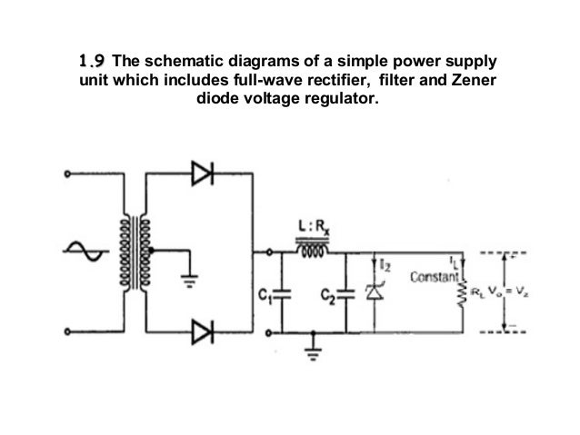
The mesh voltage is measured with an AC voltmeter on the wall outlet, on the fuse, and on the switch. If there is a 220 V AC voltage at the primary end of the transformer, then it is certain that the plug, cable, fuse and switch are in good condition.
AC signal on the secondary of the transformer can be measured on each side (secondary of transformer no CT) to ground. If there is a voltage on the secondary transformer of appropriate magnitude, then it can be ascertained that the transformer is in good condition.
Next, use the meter switch on the DC scale. Measure the voltage on C1 and on C2. If there is no DC voltage on C1 or C2, it means that the capacitor is short-circuited. When the L winding is open, then there is only a DC voltage at C1, but not in C2. When C1 and C2 are open (break), or when CR1 and CR2 directors are open, or both are short-circuited, the measured DC voltage is incorrect. Under such conditions, it is necessary to measure resistance to ensure the damaged component.
The second way is the opposite of the first way, ie starting from the measurement of DC voltage on capacitor C2, followed by measurement of DC voltage on capacitor C1 and so on. The result is the same because the measurement uses only voltmeter only.
The following example is an FM radio whose block diagram shown in figure does not work.

Examination of power supply and voltage at static state of the circuit has been done. The damage is in the area between the antenna and the audio amplifier. In the passive method, normal signals are considered to be present or known. However, since the antenna and tuning (which are thought to give normal signals to the system) are within the system itself, external signals must be assigned as normal signals and use speakers as signal indicators. This method is called an active signal-tracing method or signal injection.
First step:
The signal generator is connected to the RF tuner, and the antenna is removed; The signal generator and tuner are set at the same frequency. If you do not hear anything on the loudspeaker, move the signal generator at point A. change the frequency of the generator signal at 10.7 MHz (Standard for FM radio). When the sound is heard (tone of the generator signal), this means damage to the RF tuner.
If not heard something, move the generator signal to the amplifier output, ie at point B. At this point, the amplitude of the generator signal must be increased to compensate for the gain of the middle amplifier.
At point C, the normal signal is an audio signal. Therefore, the signal generator entered through this point must be at the audio frequency.
At point D the generator signal should be strong enough to drive the loudspeaker. The loudspeaker can be tested by checking the voltage on the amplifier driver and minimizing it momentarily with the corresponding resistor between voltage and ground. This should generate a click sound on the loudspeaker.
The second way:
The check is done from the speakers to the tuner. To determine whether using the first or second way can be preliminary, for example: by briefly amplifying the audio amplifier input with ground using a screwdriver or the end of a clip, this should produce a loudspeaker click (if the loudspeaker and audio amplifier are working properly).
If you do not hear the sound, then the second way is the best choice, because the damage must exist between the loudspeaker and the audio amplifier.
When you hear a click, you can still continue the examination in a second way from point C, or in the first way, since both have the same chance of checking speed.
Means:
The signal-tracing method requires input signals on the suspect area, and can be measured accurately. Signal-tracing always requires at least one test kit and generally two.
Methods of voltage and resistance
In general, voltage and resistance measurements are performed to check for suspected damaged tissue or components. Voltage measurements require equipment with ON conditions, whereas resistance measurements are made when the equipment is OFF.
Usually circuit diagrams and datasheets indicate the voltage required for normal operating conditions at a particular test point. By making such measurements, usually the location of damage to the network and components can be known.
Resistance measurement is a very useful method for checking electronics components. A simple resistance measurement can be used to ensure continuous wiring, the correct value approach of the transformer, inductor, winding as well as the value approach of the large capacitor.
The majority of resistors used in electronic equipment are carbon composition types and they tend to change in value due to age and heat. When this happens often perhaps the measurement of resistor resistance or other components in the circuit, should be assured by examination on the circuit image. The parallel impedance does not give an incorrect measurement, when a resistor increases in magnitude or open, it is relatively simple to determine this.
Voltage and Barrier Techniques are often used anywhere after the symptom-function technique refers to a particular circuit or component as a source of damage, or when a signaltracing technique has localized a defect in this way.
mean :Voltage and Barrier methods are used to pinpoint a component or circuit breakage and generally require company data for component and voltage values.
The half-splitting method
This method is suitable for series with series blocks / open loop system (elongated) because it will be very fast when looking for damage. For example: function generator circuit, radio transmitter / receiver, etc.
The step: starting from the center of the system, and successively on each of the middle half of the part of the system that has been separated until it is found to be damaged.
Block 1 ---> block 2 ---> block 3 ---->block 4 ----->block 5 ----> block 6 ----> block 7 ----> block8
As an insight material that in the electronics block diagram shows the signal flow, while the schematic circuit shows the flow of current and voltage, flow chart is the flow of the program or function.
8 Block Sub Serial System Series
Check the output of block 4, if it works fine, means blocks 1 through 4 there is no problem.
If it does not work, then check block 2 output (middle of blocks 1-4), and if good means check out block 3 output, and if good means block 4 is damaged.
Check Output of block 8, if it works well, means block 5 to block 8 is no problem.
If it does not work, then check the output of block 6 (middle of blocks 1-4), and if good means check out the output of block 7, and if good, then block 8 is damaged.
Loop breaking method
Electronic systems or sub-systems with feedback, very difficult to trace the damage without breaking the loop. Appropriate DC voltage or signal, shall be injected at the point where the loop is disconnected.
Voltages and signals through the circuit, should be used to monitor errors.
Inverted voltage or signal can be changed, to see the change of circuit response from normal state.
Typically, the loop is broken at the point where the signal is at small power, so it can be injected properly.
This technique can be used for example on a PLL (phase lock loop), such as :
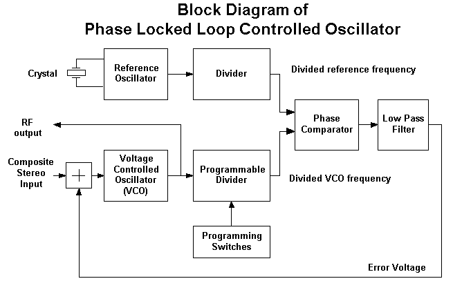
The power supply and reference oscillator output should be checked first before the loop is disconnected. In this case the output should be abnormal or unstable or missing, so we can be sure that the VCO is not good. Next we can do the loop termination at the appropriate point. So the loop termination here is not necessarily the feedback section, but is sought in small signal areas that are easily injected with existing equipment.
Substitution method
In this method it is usually necessary to sold or replace parts as the final stage of the damage tracking process.
There are two main stages in the substitution method that must be done, namely: use the correct replacement components, and connect correctly to the circuit.
Prior to the replacement, it is advisable to check with other methods as described previously, to be sure which component is damaged.
Do a voltage measurement to make sure that the voltage that is supposed to exist really exists. The voltage checks performed on the combined components of resistors and capacitors, will be able to show whether they are damaged or just one of them.
In practice, we are usually very difficult to find a replacement component in the form of ICs, transistors, and diodes that exactly match the replaced components. To solve this, you need to find equivalent data of IC type, transistor, or diode in semiconductor user manual.
If the replaced component has a special type, for example: transformer, coil-deflection yoke, and other special components, it is necessary to look for a completely suitable replacement component (no equivalent).
PRINCIPLE OF DAMAGE TRACK / FAILURE
1. Maintenance Process in Industry
2. Specifications
3. Reliability and Failure
4. Method-Tracking Method of Damage
5. Problem-Solving Analysis
6. Active Component Testing
7. Circuit Checking and Testing
X . I
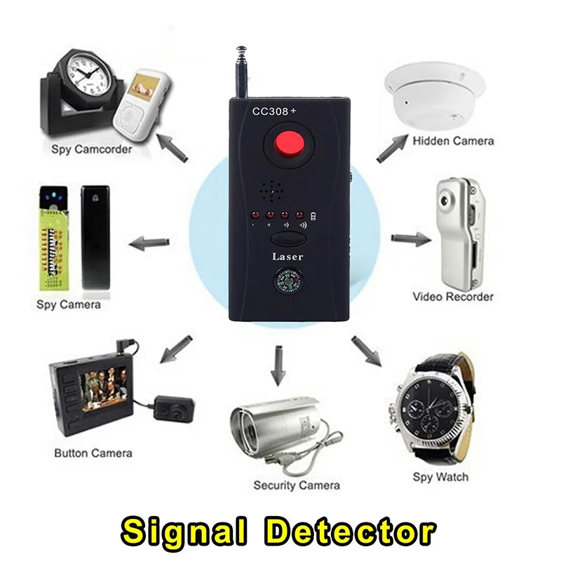
Detector (radio) / tracker
After sound (amplitude modulation, AM) transmission began around 1920, the term evolved to mean a demodulator, a nonlinear rectifier (usually a crystal diode or a vacuum tube) which extracted the audio signal from the radio frequency carrier wave. This is its current meaning, although modern detectors usually consist of semiconductor diodes, transistors, or integrated circuits.
In a superheterodyne receiver the term is also sometimes used to refer to the mixer, the tube or transistor which converts the incoming radio frequency signal to the intermediate frequency. The mixer is called the first detector, while the demodulator that extracts the audio signal from the intermediate frequency is called the second detector.

A coherer detector, useful only for Morse code signals.
Amplitude modulation detectors
Envelope detector

A simple envelope detector

A simple crystal radio with no tuned circuit can be used to listen to strong AM broadcast signals
An early form of envelope detector was the cat's whisker, which was used in the crystal set radio receiver. A later version using a crystal diode is still used in crystal radio sets today. The limited frequency response of the headset eliminates the RF component, making the low pass filter unnecessary. More sophisticated envelope detectors include the plate detector, grid-leak detector and transistor equivalents of them, infinite-impedance detectors (peak detector circuits), and precision rectifiers.
Product detector
A product detector is a type of demodulator used for AM and SSB signals, where the original carrier signal is removed by multiplying the received signal with a signal at the carrier frequency (or near to it). Rather than converting the envelope of the signal into the decoded waveform by rectification as an envelope detector would, the product detector takes the product of the modulated signal and a local oscillator, hence the name. By heterodyning, the received signal is mixed (in some type of nonlinear device) with a signal from the local oscillator, to give sum and difference frequencies to the signals being mixed, just as a first mixer stage in a superhet would produce an intermediate frequency; the beat frequency in this case, the low frequency modulating signal is recovered and the unwanted high frequencies filtered out from the output of the product detector.Product detector circuits are analog multipliers and so essentially ring modulators or synchronous detectors and closely related to some phase-sensitive detector circuits. They can be implemented using something as simple as ring of diodes or a single dual-gate Field Effect Transistor to anything as sophisticated as an Integrated Circuit containing a Gilbert cell.
Frequency and phase modulation detectors
AM detectors cannot demodulate FM and PM signals because both have a constant amplitude. However an AM radio may detect the sound of an FM broadcast by the phenomenon of slope detection which occurs when the radio is tuned slightly above or below the nominal broadcast frequency. Frequency variation on one sloping side of the radio tuning curve gives the amplified signal a corresponding local amplitude variation, to which the AM detector is sensitive. Slope detection gives inferior distortion and noise rejection compared to the following dedicated FM detectors that are normally used.Phase detector
A phase detector is a nonlinear device whose output represents the phase difference between the two oscillating input signals. It has two inputs and one output: a reference signal is applied to one input and the phase or frequency modulated signal is applied to the other. The output is a signal that is proportional to the phase difference between the two inputs.In phase demodulation the information is contained in the amount and rate of phase shift in the carrier wave.
The Foster-Seeley discriminator
The Foster-Seeley discriminator is a widely used FM detector. The detector consists of a special center-tapped transformer feeding two diodes in a full wave DC rectifier circuit. When the input transformer is tuned to the signal frequency, the output of the discriminator is zero. When there is no deviation of the carrier, both halves of the center tapped transformer are balanced. As the FM signal swings in frequency above and below the carrier frequency, the balance between the two halves of the center-tapped secondary is destroyed and there is an output voltage proportional to the frequency deviation.Ratio detector

A ratio detector using solid-state diodes
Quadrature detector
In quadrature detectors, the received FM signal is split into two signals. One of the two signals is then passed through a high-reactance capacitor, which shifts the phase of that signal by 90 degrees. This phase-shifted signal is then applied to an LC circuit, which is resonant at the FM signal's unmodulated, "center," or "carrier" frequency. If the received FM signal's frequency equals the center frequency, then the two signals will have a 90-degree phase difference and they are said to be in "phase quadrature" — hence the name of this method. The two signals are then multiplied together in an analog or digital device, which serves as a phase detector; that is, a device whose output is proportional to the phase difference between two signals. In the case of an unmodulated FM signal, the phase detector's output is — after the output has been filtered; that is, averaged over time — constant; namely, zero. However, if the received FM signal has been modulated, then its frequency will vary from the center frequency. In this case, the resonant LC circuit will further shift the phase of the signal from the capacitor, so that the signal's total phase shift will be the sum of the 90 degrees that's imposed by the capacitor and the positive or negative phase change that's imposed by the LC circuit. Now the output from the phase detector will differ from zero, and in this way, one recovers the original signal that was used to modulate the FM carrier.This detection process can also be accomplished by combining, in an exclusive-OR (XOR) logic gate, the original FM signal and a square wave whose frequency equals the FM signal's center frequency. The XOR gate produces an output pulse whose duration equals the difference between the times at which the square wave and the received FM signal pass through zero volts. As the FM signal's frequency varies from its unmodulated center frequency (which is also the frequency of the square wave), the output pulses from the XOR gate become longer or shorter. (In essence, this quadrature detector converts an FM signal into a pulse-width modulated (PWM) signal.) When these pulses are filtered, the filter's output rises as the pulses grow longer and its output falls as the pulses grow shorter. In this way, one recovers the original signal that was used to modulate the FM carrier.
Other FM detectors
Less common, specialized, or obsolescent types of detectors include:- Travis or double tuned circuit discriminator using two non-interacting tuned circuits above and below the nominal center frequency
- Weiss discriminator which uses a single LC tuned circuit or crystal
- Pulse count discriminator which converts the frequency to a train of constant amplitude pulses, producing a voltage directly proportional to the frequency.
Phase-locked loop detector
The phase-locked loop detector requires no frequency-selective LC network to accomplish demodulation. In this system, a voltage controlled oscillator (VCO) is phase locked by a feedback loop, which forces the VCO to follow the frequency variations of the incoming FM signal. The low-frequency error voltage that forces the VCO's frequency to track the frequency of the modulated FM signal is the demodulated audio output.X . II
CRYSTAL RADIO AND DETEKTOR
A crystal radio receiver, also called a crystal set or cat's whisker receiver, is a very simple radio receiver, popular in the early days of radio. It needs no other power source but that received solely from the power of radio waves received by a wire antenna. It gets its name from its most important component, known as a crystal detector, originally made from a piece of crystalline mineral such as galena. This component is now called a diode.
Crystal radios are the simplest type of radio receiver an Tutup d can be made with a few inexpensive parts, such as a wire for an antenna, a coil of copper wire for adjustment, a capacitor, a crystal detector, and earphones. Crystal radios are distinct from ordinary radios as they are passive receivers, while other radios use a separate source of electric power such as a battery or the mains power to amplify the weak radio signal so as to make it louder. Thus, crystal sets produce rather weak sound and must be listened to with sensitive earphones, and can only receive stations within a limited range.
Today they are still sold as educational devices, and there are groups of enthusiasts devoted to their construction . Crystal radios receive amplitude modulated (AM) signals, and can be designed to receive almost any radio frequency band, but most receive the AM broadcast band. A few receive shortwave bands, but strong signals are required. The first crystal sets received wireless telegraphy signals broadcast by spark-gap transmitters at frequencies as low as 20 kHz.
Bright clouds

A family listening to a crystal radio in the 1920s

Greenleaf Whittier Pickard's US Patent 836,531 "Means for receiving intelligence communicated by electric waves" diagram
Radio receiver, Basel, Switzerland, 1914

NBS Circular 120 Home Crystal Radio Project
Early years
Early radio telegraphy used spark gap and arc transmitters as well as high-frequency alternators running at radio frequencies. The coherer was the first means of detecting a radio signal. These, however, lacked the sensitivity to detect weak signals.In the early 20th century, various researchers discovered that certain metallic minerals, such as galena, could be used to detect radio signals.
Pickard's detector was revolutionary in that he found that a fine pointed wire known as a "cat's whisker", in delicate contact with a mineral, produced the best semiconductor effect (that of rectification).
A crystal detector includes a crystal, a special thin wire that contacts the crystal, and the stand that holds those components in place. The most common crystal used is a small piece of galena; pyrite was also often used, as it was a more easily adjusted and stable mineral, and quite sufficient for urban signal strengths. Several other minerals also performed well as detectors. Another benefit of crystals was that they could demodulate amplitude modulated signals. This device brought radiotelephones and voice broadcast to a public audience. Crystal sets represented an inexpensive and technologically simple method of receiving these signals at a time when the embryonic radio broadcasting industry was beginning to grow.
Crystodyne
crystodyne applying voltage biases to various kinds of crystals for manufacture of radio detectors. The result was astonishing: with a zincite (zinc oxide) crystal he gained amplification. This was negative resistance phenomenon, decades before the development of the tunnel diode. After the first experiments, Losev built regenerative and superheterodyne receivers, and even transmitters.
A crystodyne could be produced in primitive conditions; it can be made in a rural forge, unlike vacuum tubes and modern semiconductor devices. However, this discovery was not supported by authorities and soon forgotten; no device was produced in mass quantity beyond a few examples for research.
"Foxhole radios"

"Foxhole radio" used on the Italian Front in World War 2. It uses a
pencil lead attached to a safety pin pressing against a razor blade for a
detector.
Design
Block diagram of a crystal radio receiver
- An antenna in which electric currents are induced by the radio waves.
- A resonant circuit (tuned circuit) which serves to select the frequency of the desired radio station out of all the radio signals received by the antenna. The tuned circuit consists of a coil of wire (called an inductor) and a capacitor connected together, so as to create a circuit that resonates at the frequency of the desired station, and hence "tune" in that station. One or both of the coil or capacitor is adjustable, allowing the circuit to be tuned to different frequencies. In some circuits a capacitor is not used, as the antenna also serves as the capacitor. The tuned circuit has a resonant frequency and allows radio waves at that frequency to pass to the detector, while rejecting waves at all other frequencies. Such a circuit is also known as a bandpass filter.
- A semiconductor crystal (detector) that demodulates the radio signal to get the audio signal (modulation). The crystal detector is a nonlinear impedance that functions as a square law detector[citation needed]. The detector's output is converted to sound by the earphone. Early sets used a cat's whisker detector, consisting of a fine wire touching the surface of a sample of crystalline mineral such as galena. It was this component that gave crystal sets their name.
- An earphone to convert the audio signal to sound waves so they can be heard. The low power produced by a crystal receiver is insufficient to power a loudspeaker, hence earphones are used.
Pictorial diagram from 1922 showing the circuit of a crystal radio. This common circuit did not use a tuning capacitor, but used the capacitance of the antenna to form the tuned circuit
with the coil. The detector might have been a piece of galena with a
whisker wire in contact with it on a part of the crystal, making a diode
contact
Commercial passive receiver development was abandoned with the advent of reliable vacuum tubes around 1920, and subsequent crystal radio research was primarily done by radio amateurs and hobbyists. Many different circuits have been used. The following sections discuss the parts of a crystal radio in greater detail.
Antenna
The antenna converts the energy in the electromagnetic radio waves to an alternating electric current in the antenna, which is connected to the tuning coil. Since in a crystal radio all the power comes from the antenna, it is important that the antenna collect as much power from the radio wave as possible. The larger an antenna, the more power it can intercept. Antennas of the type commonly used with crystal sets are most effective when their length is close to a multiple of a quarter-wavelength of the radio waves they are receiving. Since the length of the waves used with crystal radios is very long (AM broadcast band waves are 182-566 m or 597–1857 ft. long) the antenna is made as long as possible, from a long wire, in contrast to the whip antennas or ferrite loopstick antennas used in modern radios.Serious crystal radio hobbyists use "inverted L" and "T" type antennas, consisting of hundreds of feet of wire suspended as high as possible between buildings or trees, with a feed wire attached in the center or at one end leading down to the receiver. However more often random lengths of wire dangling out windows are used. A popular practice in early days (particularly among apartment dwellers) was to use existing large metal objects, such as bedsprings, fire escapes, and barbed wire fences as antennas.
Ground
The wire antennas used with crystal receivers are monopole antennas which develop their output voltage with respect to ground. The receiver thus requires a connection to ground (the earth) as a return circuit for the current. The ground wire was attached to a radiator, water pipe, or a metal stake driven into the ground. In early days if an adequate ground connection could not be made a counterpoise was sometimes used. A good ground is more important for crystal sets than it is for powered receivers, as crystal sets are designed to have a low input impedance needed to transfer power efficiently from the antenna. A low resistance ground connection (preferably below 25 Ω) is necessary because any resistance in the ground reduces available power from the antenna. In contrast, modern receivers are voltage-driven devices, with high input impedance, hence little current flows in the antenna/ground circuit. Also, mains powered receivers are grounded adequately through their power cords, which are in turn attached to the earth by way of a well established ground.Tuned circuit


The antenna is an integral part of the tuned circuit and its reactance contributes to determining the circuit's resonant frequency. Antennas usually act as a capacitance, as antennas shorter than a quarter-wavelength have capacitive reactance. Many early crystal sets did not have a tuning capacitor, and relied instead on the capacitance inherent in the wire antenna (in addition to significant parasitic capacitance in the coil) to form the tuned circuit with the coil.
The earliest crystal receivers did not have a tuned circuit at all, and just consisted of a crystal detector connected between the antenna and ground, with an earphone across it. Since this circuit lacked any frequency-selective elements besides the broad resonance of the antenna, it had little ability to reject unwanted stations, so all stations within a wide band of frequencies were heard in the earphone (in practice the most powerful usually drowns out the others). It was used in the earliest days of radio, when only one or two stations were within a crystal set's limited range.
Impedance matching
"Two 
 slider" crystal radio circuit.
and example from 1920s. The two sliding contacts on the coil allowed
the impedance of the radio to be adjusted to match the antenna as theradio was tuned, resulting in stronger reception
slider" crystal radio circuit.
and example from 1920s. The two sliding contacts on the coil allowed
the impedance of the radio to be adjusted to match the antenna as theradio was tuned, resulting in stronger reception
slider" crystal radio circuit.
and example from 1920s. The two sliding contacts on the coil allowed
the impedance of the radio to be adjusted to match the antenna as theradio was tuned, resulting in stronger receptionTherefore, in improved receiver circuits, in order to match the antenna impedance to the receiver's impedance, the antenna was connected across only a portion of the tuning coil's turns. This made the tuning coil act as an impedance matching transformer (in an autotransformer connection) in addition to providing the tuning function. The antenna's low resistance was increased (transformed) by a factor equal to the square of the turns ratio (the ratio of the number of turns the antenna was connected to, to the total number of turns of the coil), to match the resistance across the tuned circuit. In the "two-slider" circuit, popular during the wireless era, both the antenna and the detector circuit were attached to the coil with sliding contacts, allowing (interactive) adjustment of both the resonant frequency and the turns ratio. Alternatively a multiposition switch was used to select taps on the coil. These controls were adjusted until the station sounded loudest in the earphone.
Problem of selectivity

Direct-coupled circuit with impedance matching
The crystal detector worsened the problem, because it has relatively low resistance, thus it "loaded" the tuned circuit, damping the oscillations (lowering the response), and reducing its Q. In many circuits, the selectivity was improved by connecting the detector and earphone circuit to a tap across only a fraction of the coil's turns. This reduced the impedance loading of the tuned circuit, as well as improving the impedance match with the detector.
Inductive coupling

Inductively-coupled circuit with impedance matching. This type was used in most quality crystal receivers

Amateur-built crystal receiver with "loose coupler" antenna transformer, Belfast, around 1914
Reducing the coupling between the coils, by physically separating them so that less of the magnetic field of one intersects the other, reduces the mutual inductance, narrows the bandwidth, and results in much sharper, more selective tuning than that produced by a single tuned circuit. However, the looser coupling also reduced the power of the signal passed to the second circuit. The transformer was made with adjustable coupling, to allow the listener to experiment with various settings to gain the best reception.
One design common in early days, called a "loose coupler", consisted of a smaller secondary coil inside a larger primary coil. The smaller coil was mounted on a rack so it could be slid linearly in or out of the larger coil. If radio interference was encountered, the smaller coil would be slid further out of the larger, loosening the coupling, narrowing the bandwidth, and thereby rejecting the interfering signal.
The antenna coupling transformer also functioned as an impedance matching transformer, that allowed a better match of the antenna impedance to the rest of the circuit. One or both of the coils usually had several taps which could be selected with a switch, allowing adjustment of the number of turns of that transformer and hence the "turns ratio".
Coupling transformers were difficult to adjust, because the three adjustments, the tuning of the primary circuit, the tuning of the secondary circuit, and the coupling of the coils, were all interactive, and changing one affected the others.
Crystal detector
Galena cat's whisker detector

Germanium diode used in modern crystal radios (about 3 mm long)

How the crystal detector works. (A) The amplitude modulated radio signal from the tuned circuit. The rapid oscillations are the radio frequency carrier wave. The audio signal (the sound) is contained in the slow variations (modulation)
of the amplitude (hence the term amplitude modulation, AM) of the
waves. This signal cannot be converted to sound by the earphone, because
the audio excursions are the same on both sides of the axis, averaging
out to zero, which would result in no net motion of the earphone's
diaphragm. (B) The crystal
conducts current better in one direction than the other, producing a
signal whose amplitude does not average to zero but varies with the
audio signal. (C) A bypass capacitor is used to remove the radio frequency carrier pulses, leaving the audio signal

Circuit with detector bias battery to improve sensitivity and buzzer to adjust cat's whisker
In a cat's whisker detector only certain sites on the crystal surface functioned as rectifying junctions, and the device was very sensitive to the pressure of the crystal-wire contact, which could be disrupted by the slightest vibration. Therefore, a usable contact point had to be found by trial and error before each use. The operator dragged the wire across the crystal surface until a radio station or "static" sounds were heard in the earphones. Alternatively, some radios (circuit, right) used a battery-powered buzzer attached to the input circuit to adjust the detector. The spark at the buzzer's electrical contacts served as a weak source of static, so when the detector began working, the buzzing could be heard in the earphones. The buzzer was then turned off, and the radio tuned to the desired station.
Galena (lead sulfide) was probably the most common crystal used in cat's whisker detectors, but various other types of crystals were also used, the most common being iron pyrite (fool's gold, FeS2), silicon, molybdenite (MoS2), silicon carbide (carborundum, SiC), and a zincite-bornite (ZnO-Cu5FeS4) crystal-to-crystal junction trade-named Perikon. Crystal radios have also been improvised from a variety of common objects, such as blue steel razor blades and lead pencils, rusty needles, and pennies In these, a semiconducting layer of oxide or sulfide on the metal surface is usually responsible for the rectifying action.
In modern sets, a semiconductor diode is used for the detector, which is much more reliable than a cat's whisker detector and requires no adjustments. Germanium diodes (or sometimes Schottky diodes) are used instead of silicon diodes, because their lower forward voltage drop (roughly 0.3V compared to 0.6V ) makes them more sensitive.
All semiconductor detectors function rather inefficiently in crystal receivers, because the low voltage input to the detector is too low to result in much difference between forward better conduction direction, and the reverse weaker conduction. To improve the sensitivity of some of the early crystal detectors, such as silicon carbide, a small forward bias voltage was applied across the detector by a battery and potentiometer. The bias moves the diode's operating point higher on the detection curve producing more signal voltage at the expense of less signal current (higher impedance). There is a limit to the benefit that this produces, depending on the other impedances of the radio. This improved sensitivity was caused by moving the DC operating point to a more desirable voltage-current operating point (impedance) on the junction's I-V curve. The battery did not power the radio, but only provided the biasing voltage which required little power.
Earphones

Modern crystal radio with piezoelectric earphone
The early earphones used with wireless-era crystal sets had moving iron drivers that worked in a way similar to the horn loudspeakers of the period; modern loudspeakers use a moving-coil principle. Each earpiece contained a permanent magnet about which was a coil of wire which formed a second electromagnet. Both magnetic poles were close to a steel diaphram of the speaker. When the audio signal from the radio was passed through the electromagnet's windings, current was caused to flow in the coil which created a varying magnetic field that augmented or diminished that due to the permanent magnet. This varied the force of attraction on the diaphragm, causing it to vibrate. The vibrations of the diaphragm push and pull on the air in front of it, creating sound waves. Standard headphones used in telephone work had a low impedance, often 75 Ω, and required more current than a crystal radio could supply. Therefore, the type used with crystal set radios (and other sensitive equipment) was wound with more turns of finer wire giving it a high impedance of 2000-8000 Ω.
Modern crystal sets use piezoelectric crystal earpieces, which are much more sensitive and also smaller. They consist of a piezoelectric crystal with electrodes attached to each side, glued to a light diaphragm. When the audio signal from the radio set is applied to the electrodes, it causes the crystal to vibrate, vibrating the diaphragm. Crystal earphones are designed as ear buds that plug directly into the ear canal of the wearer, coupling the sound more efficiently to the eardrum. Their resistance is much higher (typically megohms) so they do not greatly "load" the tuned circuit, allowing increased selectivity of the receiver. The piezoelectric earphone's higher resistance, in parallel with its capacitance of around 9 pF, creates a filter that allows the passage of low frequencies, but blocks the higher frequencies. In that case a bypass capacitor is not needed (although in practice a small one of around 0.68 to 1 nF is often used to help improve quality), but instead a 10-100 kΩ resistor must be added in parallel with the earphone's input.
Although the low power produced by crystal radios is typically insufficient to drive a loudspeaker, some homemade 1960s sets have used one, with an audio transformer to match the low impedance of the speaker to the circuit. Similarly, modern low-impedance (8 Ω) earphones cannot be used unmodified in crystal sets because the receiver does not produce enough current to drive them. They are sometimes used by adding an audio transformer to match their impedance with the higher impedance of the driving antenna circuit.
Use as a power source
A crystal radio tuned to a strong local transmitter can be used as a power source for a second amplified receiver of a distant station that cannot be heard without amplification.There is a long history of unsuccessful attempts and unverified claims to recover the power in the carrier of the received signal itself. Traditional crystal sets use half-wave rectifiers. As AM signals have a modulation factor of only 30% by voltage at peaks, no more than 9% of received signal power (
 )
is actual audio information, and 91% is just rectified DC voltage.
Given that the audio signal is unlikely to be at peak all the time, the
ratio of energy is, in practice, even greater. Considerable effort was
made to convert this DC voltage into sound energy. Some earlier attempts
include a one-transistor
amplifier in 1966. Sometimes efforts to recover this power are confused
with other efforts to produce a more efficient detection. This history continues now with designs as elaborate as "inverted two-wave switching power unit".
)
is actual audio information, and 91% is just rectified DC voltage.
Given that the audio signal is unlikely to be at peak all the time, the
ratio of energy is, in practice, even greater. Considerable effort was
made to convert this DC voltage into sound energy. Some earlier attempts
include a one-transistor
amplifier in 1966. Sometimes efforts to recover this power are confused
with other efforts to produce a more efficient detection. This history continues now with designs as elaborate as "inverted two-wave switching power unit". X . IIII
Electro-optical sensor
in detector aplication
- Lamps that turn on automatically in response to darkness
- Position sensors that activate when an object interrupts a light beam
- Flash detection, to synchronize one photographic flash to another
- Photoelectric sensors that detect the distance, absence, or presence of an object
Function
An optical sensor converts light rays into electronic signals. It measures the physical quantity of light and then translates it into a form that is readable by an instrument. An optical sensor is generally part of a larger system that integrates a source of light, a measuring device and the optical sensor. This is often connected to an electrical trigger. The trigger reacts to a change in the signal within the light sensor. An optical sensor can measure the changes from one or several light beams. When a change occurs, the light sensor operates as a photoelectric trigger and therefore either increases or decreases the electrical output. An optical switch enables signals in optical fibres or integrated optical circuits to be switched selectively from one circuit to another. An optical switch can operate by mechanical means or by electro-optic effects, magneto-optic effects as well as by other methods. Optical switches are optoelectronic devices which can be integrated with integrated or discrete microelectronic circuits.Types of Optical Sensors and Switches
There are many different kinds of optical sensors, the most common types are:- Photoconductive devices convert a change of incident light into a change of resistance.
- Photovoltaics, commonly known as solar cells, convert an amount of incident light into an output voltage.
- Photodiodes convert an amount of incident light into an output current.
- Phototransistors are a type of bipolar transistor where the base-collector junction is exposed to light. This results in the same behaviour of a photodiode, but with an internal gain.
Applications
Electro-optical sensors are used whenever light needs to be converted to energy. Because of this, electro-optical sensors can be seen almost anywhere. Common applications are smartphones where sensors are used to adjust screen brightness, and smartwatches in which sensors are used to measure the wearer's heartbeat.Optical sensors can be found in the energy field to monitor structures that generate, produce, distribute, and convert electrical power. The distributed and nonconductive nature of optical fibres makes optical sensors perfect for oil and gas applications, including pipeline monitoring. They can also be found in wind turbine blade monitoring, offshore platform monitoring, power line monitoring and downhole monitoring. Other applications include the civil and transportation fields such as bridge, airport landing strip, dam, railway, airplane, wing, fuel tank and ship hull monitoring.
Among other applications, optical switches can be found in thermal methods which vary the refraction index in one leg of an interferometer in order to switch the signal, MEMS approaches involving arrays of micromirrors that can deflect an optical signal to the appropriate receiver, piezoelectric beam steering liquid crystals which rotate polarized light depending on the applied electric field and acousto-optic methods which change the refraction index as a result of strain induced by an acoustic field to deflect light.
Another important application of optical sensor is to measure the concentration of different compounds by both visible and infrared spectroscopy.
Light fixture

A large number of light fixtures and lamps at a store.

Ceiling light fixtures
Portable light fixtures are often called "lamps", as in table lamp or desk lamp. In technical terminology, the lamp is the light source, which is typically called the light bulb. The term luminaire is recommended by the International Electrotechnical Commission (IEC) for technical use.
a bright cloud

Industrial light fixture, designed by Peter Behrens, around 1915
Fixture types
Light fixtures are classified by how the fixture is installed, the light function or lamp type.Free-standing or portable

Tiffany dragonfly desk lamp with pigeon sculptures
- Table lamp fixtures, standard lamp fixtures, and office task light luminaires.
- Balanced-arm lamp is a spot light with an adjustable arm such as anglepoise or Luxo L1.
- Gooseneck lamp
- Nightlight
- Floor Lamp
- Torch lamp or torchières are floor lamps with an upward facing shade. They provide general lighting to the rest of the room.
- Gooseneck lamp
- Bouillotte lamp: see Bouillotte
Fixed
- Ceiling Dome — Also called the light source(s) are hidden behind a
translucent dome typically made of glass, with some combination of
frosting and surface texturing to diffuse the light. These can be flush
mount fixtures which are mounted right up against the ceiling, or
semi-flush fixtures which are separated by a small distance (usually
about 3-12").
- Open ceiling dome — the translucent dome is suspended a short distance below the ceiling by a mechanism that is hidden with the exception of a screw-knob or other device appearing on the outer dome face, and pulling this knob releases the dome
- Enclosed ceiling dome The translucent dome mates with a ring that is mounted flush with the ceiling
- Recessed light
— the protective housing is concealed behind a ceiling or wall, leaving
only the fixture itself exposed. The ceiling-mounted version is often
called a downlight.
- "Cans" with a variety of lamps — this term is jargon for inexpensive downlighting products that are recessed into the ceiling, or sometimes for uplights placed on the floor. The name comes from the shape of the housing. The term "pot lights" is often used in Canada and parts of the US.
- Cove light — recessed into the ceiling in a long box against a wall.
- Troffer — recessed fluorescent light fixtures, usually rectangular in shape to fit into a drop ceiling grid.

A chandelier light fixture
- Surface-mounted light — the finished housing is exposed, not flush with surface
- Chandelier
- Pendant light — suspended from the ceiling with a chain or pipe
- Sconce — provide up or down lights; can be used to illuminate artwork, architectural details; commonly used in hallways or as an alternative to overhead lighting.
- Track lighting fixture — individual fixtures ("track heads") can be positioned anywhere along the track, which provides electric power.
- Under-cabinet light — mounted below kitchen wall cabinets
- Display Case or Showcase light — shows merchandise on display within an enclosed case such as jewelry, grocery stores, and chain stores.
- Ceiling fan - May sometimes have a light, often referred to as a light kit mounted to it.
- Emergency lighting or exit sign — connected to a battery backup or to an electric circuit that has emergency power if the mains power fails
- High- and low-bay lighting — typically used for general lighting for industrial buildings and often big-box stores
- Strip lights or Industrial lighting — often long lines of fluorescent lamps used in a warehouse or factory

A decorative outdoor lamp at Leeds Town Hall.

A garden solar lamp is an example of landscape lighting
- Outdoor lighting and landscape lighting — used to illuminate walkways, parking lots, roadways, building exteriors and architectural details, gardens, and parks.
- High-mast, usually pole- or stanchion-mounted — for landscape, roadways, and parking lots
- Bollard — A type of architectural outdoor lighting that is a short, upright ground-mounted unit typically used to provide cutoff type illumination for egress lighting, to light walkways, steps, or other pathways.
- Solar lamp
- Street light
- Yard light
Special-purpose lights
- Accent light — Any directional light which highlights an object or attracts attention to a particular area
- Background light — for use in video production
- Blacklight
- Christmas lights-also called fairy lights or twinkle lights and are often used at Christmas and other holidays for decoration.
- Flood light
- Safelight (for use in a darkroom)
- Safety lamp (for use in coal mines)
- Searchlight (for military and advertising use)
- Security lighting
- Step light
- Strobe light
- Task light
- Traffic light
- Theatrical
- Wallwasher
Lamp types

Old table lamps at Archaeological Museum, Sri Lanka
- Fuel lamps
- Betty lamp, butter lamp, carbide lamp, gas lighting, kerosene lamp, oil lamp, rush light, torch, candle, Limelight, gas mantle
- Safety lamps: Davy lamp & Geordie lamp
- Mercury-vapor lamp, Metal-halide (HMI, HQI, CDM), Sodium vapor or "high-pressure sodium"
- A-lamp, Parabolic aluminized reflector lamp (PAR), reflector lamp (R), bulged reflector lamp (BR) (refer to lamp shapes)
- Obsolete types: limelight, carbon button lamp, Mazda (light bulb), Nernst glower
- Novelty: Lava lamp
- Special purpose: heat lamp, Globar, gas mantle
- Halogen – special class of incandescent lamps
- Nuclear: self-powered lighting
- Plasma lamp
- Light-emitting diode (LED) (solid-state lighting)

Table Lighting
Light-fixture controls
- 3-way 2-circuit switch
- Dimmer (this allows the user to make a light brighter or dimmer, typically using a rotary dial)
- Light switch (often part of the light socket or power cord on portable fixtures)
- Lighting control system
- Motion detector
- Timer
- Touch
- X10 (industry standard) systems
Position sensor :
Some position sensors available today:
- Capacitive transducer
- Capacitive displacement sensor
- Eddy-current sensor
- Ultrasonic sensor
- Grating sensor
- Hall effect sensor
- Inductive non-contact position sensors
- Laser Doppler Vibrometer (optical)
- Linear variable differential transformer (LVDT)
- Multi-axis displacement transducer
- Photodiode array
- Piezo-electric transducer (piezo-electric)
- Potentiometer
- Proximity sensor (optical)
- Rotary encoder (angular)
- Seismic displacement pick-up
- String potentiometer (also known as string pot., string encoder, cable position transducer)
Flash (photography)

The high-speed wing action of a hummingbird hawk-moth is frozen by flash. The flash has given the foreground more illumination than the background. See Inverse-square law.

Video demonstration of high speed flash photography.
Flash units are commonly built directly into a camera. Some cameras allow separate flash units to be mounted via a standardized "accessory mount" bracket (a hot shoe). In professional studio equipment, flashes may be large, standalone units, or studio strobes, powered by special battery packs or connected to mains power. They are either synchronized with the camera using a flash synchronization cable or radio signal, or are light-triggered, meaning that only one flash unit needs to be synchronized with the camera, and in turn triggers the other units, called slaves.
Types of flash
Flash-lamp

Demonstration of a magnesium flash powder lamp from 1909

Vintage AHA smokeless flash powder lamp kit, Germany
Flashbulbs

Ernst Leitz Wetzlar flash from 1950s

Flashbulbs have ranged in size from the diminutive AG-1 to the massive No. 75.

Kodak Brownie Hawkeye with "Kodalite Flasholder" and Sylvania P25 blue-dot daylight-type flashbulb

The AG-1 flashbulb, introduced in 1958, used wires protruding from its
base as electrical contacts; this eliminated the need for a separate
metal base.
Flashcubes, Magicubes and Flipflash

Flashcube fitted to a Kodak Instamatic camera, showing both unused (left) and used (right) bulbs

Undersides of Flashcube (left) and Magicube (right) cartridges

"Flip flash" type cartridge
Electronic flash
Electronic flash was developed in the late 1950s while flashbulbs were still in general use. Early units were expensive and often large and heavy as the power unit was a separate unit to the flash gun head and was powered by a large lead-acid battery, and usually carried by the photographer by means of a shoulder strap. Towards the end of the 1960s, the size had dropped to the point where they were matching the size of conventional bulb flash guns (though the price, having dropped, was still an obstacle). The electronic flash system eventually superseded bulb guns as prices came down, rendering flashbulbs virtually obsolete.A typical electronic flash unit has electronic circuitry to charge a high-capacity capacitor to several hundred volts. When the flash is triggered by the shutter's flash synchronization contact, the capacitor is discharged almost instantaneously through a flash tube, producing a flash of very brief duration almost instantaneously (i.e., the flash duration, often around 1/1000 of a second, is shorter than most practical shutter speeds, and full brightness is reached before the shutter has time to close appreciably). Synchronization of full flash brightness with maximum shutter opening was problematic with bulbs which took an appreciable time to ignite and reach full brightness; electronic flash does not have these difficulties.
Simple electronic flash units are often mounted on or near the camera; many inexpensive cameras have an electronic flash unit built in.

Two professional xenon tube flashes
In a photographic studio, more powerful and flexible studio flash systems are used. They usually contain a modeling light, an incandescent light bulb close to the flash tube; the continuous illumination of the modeling light lets the photographer visualize the effect of the flash. A system may comprise multiple synchronised flashes for multi-source lighting.
The strength of a flash device is often indicated in terms of a guide number designed to simplify exposure setting. The energy released by larger studio flash units, such as monolights, is indicated in watt-seconds.
The Nikon brand name for its electronic flash units, Speedlight, is frequently used as a generic term for electronic flash equipment.
High speed flash
An air-gap flash is a high-voltage device that discharges a flash of light with an exceptionally short duration, often much less than one microsecond. These are commonly used by scientists or engineers for examining extremely fast-moving objects or reactions, famous for producing images of bullets tearing through light bulbs and balloons (see Harold Eugene Edgerton). An example of a process by which to create a high speed flash is the exploding wire method.
A photo of a Smith & Wesson Model 686 firing, taken with a high speed air-gap flash.
The photo was taken in a darkened room, with camera's shutter open and
the flash was triggered by the sound of the shot using a microphone.
Multi-flash
A camera that implements multiple flashes can be used to find depth edges or create stylized images. Such a camera has been developed by researchers at the Mitsubishi Electric Research Laboratories (MERL). Successive flashing of strategically placed flash mechanisms results in shadows along the depths of the scene. This information can be manipulated to suppress or enhance details or capture the intricate geometric features of a scene (even those hidden from the eye), to create a non-photorealistic image form. Such images could be useful in technical or medical imaging.Flash intensity
Unlike flashbulbs, the intensity of an electronic flash can be adjusted on some units. To do this, smaller flash units typically vary the capacitor discharge time, whereas larger (e.g., higher power, studio) units typically vary the capacitor charge. Color temperature can change as a result of varying the capacitor charge, thus making color corrections necessary. Due to advances in semiconductor technology, some studio units can now control intensity by varying the discharge time and thereby provide consistent color temperature.Flash intensity is typically measured in stops or in fractions (1, 1/2, 1/4, 1/8 etc.). Some monolights display an "EV Number", so that a photographer can know the difference in brightness between different flash units with different watt-second ratings. EV10.0 is defined as 6400 watt-seconds, and EV9.0 is one stop lower, i.e. 3200 watt-seconds.
Flash duration
Flash duration is commonly described by two numbers that are expressed in fractions of a second:- t.1 is the length of time the light intensity is above 0.1 (10%) of the peak intensity
- t.5 is the length of time the light intensity is above 0.5 (50%) of the peak intensity
In cases where intensity is controlled by capacitor discharge time, t.5 and t.1 decrease with decreasing intensity. Conversely, in cases where intensity is controlled by capacitor charge, t.5 and t.1 increase with decreasing intensity due to the non-linearity of the capacitor's discharge curve.
Flash LED used in phones
High-current flash LEDs are used as flash sources in camera phones, although they are not yet at the power levels to equal xenon flash devices (that are rarely used in phones) in still cameras. The major advantages of LEDs over xenon include low voltage operation, higher efficiency, and extreme miniaturization. The LED flash can also be used for illumination of video recordings or as an autofocus assist lamp in low-light conditions.Focal-plane-shutter synchronization
Electronic flash units have compatibility issues with focal-plane shutters. Focal-plane shutters expose using two curtains that cross the sensor. The first one opens and the second curtain follows it after a delay equal to the nominal shutter speed. A typical modern focal-plane shutter takes about 1/200 s to cross the sensor, so at exposure times shorter than this only part of the sensor is uncovered at any one time. Electronic flash can have durations as short as 50 µs, so at such short exposure times only part of the sensor is exposed. This limits the shutter speed to about 1/200 s when using flash. In the past, slow-burning single-use flash bulbs allowed the use of focal-plane shutters at maximum speed because they produced continuous light for the time taken for the exposing slit to cross the film gate. If these are found they cannot be used on modern cameras because the bulb must be fired *before* the first shutter curtain begins to move (M-sync); the X-sync used for electronic flash normally fires only when the first shutter curtain reaches the end of its travel.High-end flash units address this problem by offering a mode, typically called FP sync or HSS (High Speed Sync), which fires the flash tube multiple times during the time the slit traverses the sensor. Such units require communication with the camera and are thus dedicated to a particular camera make. The multiple flashes result in a significant decrease in guide number, since each is only a part of the total flash power, but it's all that illuminates any particular part of the sensor. In general, if s is the shutter speed, and t is the shutter traverse time, the guide number reduces by √s / t. For example, if the guide number is 100, and the shutter traverse time is 5 ms (a shutter speed of 1/200s), and the shutter speed is set to 1/2000 s (0.5 ms), the guide number reduces by a factor of √0.5 / 5, or about 3.16, so the resultant guide number at this speed would be about 32.
Current (2010) flash units frequently have much lower guide numbers in HSS mode than in normal modes, even at speeds below the shutter traverse time. For example, the Mecablitz 58 AF-1 digital flash unit has a guide number of 58 in normal operation, but only 20 in HSS mode, even at low speeds.
Technique

Image exposed without additional lighting (left) and with fill flash (right)

Lighting produced by direct flash (left) and bounced flash (right)
- Softboxes, diffusers that cover the flash lamp, scatter direct light and reduce its harshness.
- Reflectors, including umbrellas, flat-white backgrounds, drapes and reflector cards are commonly used for this purpose (even with small hand-held flash units).
- Bounce flash is a related technique in which flash is directed onto a reflective surface, for example a white ceiling or a flash umbrella, which then reflects light onto the subject. It can be used as fill-flash or, if used indoors, as ambient lighting for the whole scene. Bouncing creates softer, less artificial-looking illumination than direct flash, often reducing overall contrast and expanding shadow and highlight detail, and typically requires more flash power than direct lighting. Part of the bounced light can be also aimed directly on the subject by "bounce cards" attached to the flash unit which increase the efficiency of the flash and illuminate shadows cast by light coming from the ceiling. It's also possible to use one's own palm for that purpose, resulting in warmer tones on the picture, as well as eliminating the need to carry additional accessories.
- Fill flash or "fill-in flash" describes flash used to supplement ambient light in order to illuminate a subject close to the camera that would otherwise be in shade relative to the rest of the scene. The flash unit is set to expose the subject correctly at a given aperture, while shutter speed is calculated to correctly expose for the background or ambient light at that aperture setting. Secondary or slave flash units may be synchronized to the master unit to provide light from additional directions. The slave units are electrically triggered by the light from the master flash. Many small flashes and studio monolights have optical slaves built in. Wireless radio transmitters, such as PocketWizards, allow the receiver unit to be around a corner, or at a distance too far to trigger using an optical sync.
- Strobe: Some high end units can be set to flash a specified number of times at a specified frequency. This allows action to be frozen multiple times in a single exposure.
- Colored gels can also be used to change the color of the flash. Correction gels are commonly used, so that the light of the flash is the same as tungsten lights (using a CTO gel) or fluorescent lights.
- Open flash, Free flash or manually-triggred flash refers to modes in which the photographer manually triggers the flash unit to fire independently of the shutter.
Drawbacks

Flash

No flash
Left:
the distance limitation as seen when taking picture of the wooden
floor. Right: the same picture taken with incandescent ambient light,
using a longer exposure and a higher ISO speed setting. The distance is
no longer restricted, but the colors are unnatural because of a lack of
color temperature compensation, and the picture may suffer from more
grain or noise.

Using a flash in a museum is mostly prohibited.
- Using on-camera flash will give a very harsh light, which results in a loss of shadows in the image, because the only lightsource is in practically the same place as the camera. Balancing the flash power and ambient lighting or using off-camera flash can help overcome these issues. Using an umbrella or softbox (the flash will have to be off-camera for this) makes softer shadows.
- A typical problem with cameras using built-in flash units is the low intensity of the flash; the level of light produced will often not suffice for good pictures at distances of over 3 metres (10 ft) or so. Dark, murky pictures with excessive image noise or "grain" will result. In order to get good flash pictures with simple cameras, it is important not to exceed the recommended distance for flash pictures. Larger flashes, especially studio units and monoblocks, have sufficient power for larger distances, even through an umbrella, and can even be used against sunlight at short distances.
- The "red-eye effect" is another problem with on camera and ring flash units. Since the retina of the human eye reflects red light straight back in the direction it came from, pictures taken from straight in front of a face often exhibit this effect. It can be somewhat reduced by using the "red eye reduction" found on many cameras (a pre-flash that makes the subject's irises contract). However, very good results can be obtained only with a flash unit that is separated from the camera, sufficiently far from the optical axis, or by using bounce flash, where the flash head is angled to bounce light off a wall, ceiling or reflector.
- On some cameras the flash exposure measuring logic fires a pre-flash very quickly before the real flash. In some camera/people combinations this will lead to shut eyes in every picture taken. The blink response time seems to be around 1/10 of a second. If the exposure flash is fired at approximately this interval after the TTL measuring flash, people will be squinting or have their eyes shut. One solution may be the FEL (flash exposure lock) offered on some more expensive cameras, which allows the photographer to fire the measuring flash at some earlier time, long (many seconds) before taking the real picture. Unfortunately many camera manufacturers do not make the TTL pre-flash interval configurable.
- Flash distracts people, limiting the number of pictures that can be taken without irritating them.
- Photographing with flash may not be permitted in some museums even after purchasing a permit for taking pictures.
- Flash equipment may take some time to set up, and like any grip equipment, may need to be carefully secured, especially if hanging overhead, so it does not fall on anyone. A small breeze can easily topple a flash with an umbrella on a lightstand if it is not tied down or sandbagged. Larger equipment (e.g. monoblocks) will need a supply of AC power.
Photoelectric sensor

Conceptual through-beam system to detect unauthorized access to a secure
door. If the beam is damaged, the detector triggers an alarm .
Types
A self-contained photoelectric sensor contains the optics, along with the electronics. It requires only a power source. The sensor performs its own modulation, demodulation, amplification, and output switching. Some self-contained sensors provide such options as built-in control timers or counters. Because of technological progress, self-contained photoelectric sensors have become increasingly smaller.Remote photoelectric sensors used for remote sensing contain only the optical components of a sensor. The circuitry for power input, amplification, and output switching are located elsewhere, typically in a control panel. This allows the sensor, itself, to be very small. Also, the controls for the sensor are more accessible, since they may be bigger.
When space is restricted or the environment too hostile even for remote sensors, fiber optics may be used. Fiber optics are passive mechanical sensing components. They may be used with either remote or self-contained sensors. They have no electrical circuitry and no moving parts, and can safely pipe light into and out of hostile environments.
Sensing modes
A through beam arrangement consists of a receiver located within the line-of-sight of the transmitter. In this mode, an object is detected when the light beam is blocked from getting to the receiver from the transmitter.A retroreflective arrangement places the transmitter and receiver at the same location and uses a reflector to bounce the light beam back from the transmitter to the receiver. An object is sensed when the beam is interrupted and fails to reach the receiver.
A proximity-sensing (diffused) arrangement is one in which the transmitted radiation must reflect off the object in order to reach the receiver. In this mode, an object is detected when the receiver sees the transmitted source rather than when it fails to see it. As in retro-reflective sensors, diffuse sensor emitters and receivers are located in the same housing. But the target acts as the reflector, so that detection of light is reflected off the disturbance object. The emitter sends out a beam of light (most often a pulsed infrared, visible red, or laser) that diffuses in all directions, filling a detection area. The target then enters the area and deflects part of the beam back to the receiver. Detection occurs and output is turned on or off when sufficient light falls on the receiver.
Some photo eyes have two different operational types, light operate and dark operate. Light operate photo eyes become operational when the receiver "receives" the transmitter signal. Dark operate photo eyes become operational when the receiver "does not receive" the transmitter signal.
The detecting range of a photoelectric sensor is its "field of view", or the maximum distance from which the sensor can retrieve information, minus the minimum distance. A minimum detectable object is the smallest object the sensor can detect. More accurate sensors can often have minimum detectable objects of minuscule size.

Certain types of smoke detector use a photoelectric sensor to warn of smoldering fires.
Difference Between Modes
| Name | Advantages | Disadvantages |
|---|---|---|
| Through-Beam |
|
|
| Reflective |
|
|
| Diffuse |
|
|
List of sensors
- Geophone
- Hydrophone
- Lace Sensor a guitar pickup
- Microphone
- Seismometer
Automotive, transportation
- Air flow meter
- Air–fuel ratio meter
- AFR sensor
- Blind spot monitor
- Crankshaft position sensor
- Curb feeler
- Defect detector
- Engine coolant temperature sensor
- Hall effect sensor
- Knock sensor
- MAP sensor
- Mass flow sensor
- Oxygen sensor
- Parking sensors
- Radar gun
- Speedometer
- Speed sensor
- Throttle position sensor
- Tire-pressure monitoring sensor
- Torque sensor
- Transmission fluid temperature sensor,
- Turbine speed sensor
- Variable reluctance sensor
- Vehicle speed sensor
- Water sensor
- Wheel speed sensor
Chemical
- Breathalyzer
- Carbon dioxide sensor
- Carbon monoxide detector
- Catalytic bead sensor
- Chemical field-effect transistor
- Chemiresistor
- Electrochemical gas sensor
- Electronic nose
- Electrolyte–insulator–semiconductor sensor
- Fluorescent chloride sensors
- Holographic sensor
- Hydrocarbon dew point analyzer
- Hydrogen sensor
- Hydrogen sulfide sensor
- Infrared point sensor
- Ion-selective electrode
- Nondispersive infrared sensor
- Microwave chemistry sensor
- Nitrogen oxide sensor
- Olfactometer
- Optode
- Oxygen sensor
- Ozone monitor
- Pellistor
- pH glass electrode
- Potentiometric sensor
- Redox electrode
- Smoke detector
- Zinc oxide nanorod sensor
Electric current, electric potential, magnetic, radio
- Current sensor
- Daly detector
- Electroscope
- Electron multiplier
- Faraday cup
- Galvanometer
- Hall effect sensor
- Hall probe
- Magnetic anomaly detector
- Magnetometer
- Magnetoresistance
- MEMS magnetic field sensor
- Metal detector
- Planar Hall sensor
- Radio direction finder
- Voltage detector
Environment, weather, moisture, humidity
- Actinometer
- Air pollution sensor
- Bedwetting alarm
- Ceilometer
- Dew warning
- Electrochemical gas sensor
- Fish counter
- Frequency domain sensor
- Gas detector
- Hook gauge evaporimeter
- Humistor
- Hygrometer
- Leaf sensor
- Lysimeter
- Pyranometer
- Pyrgeometer
- Psychrometer
- Rain gauge
- Rain sensor
- Seismometers
- SNOTEL
- Snow gauge
- Soil moisture sensor
- Stream gauge
- Tide gauge
Flow, fluid velocity
Ionizing radiation, subatomic particles
- Cloud chamber
- Geiger counter
- Geiger-Muller tube
- Ionisation chamber
- Neutron detection
- Proportional counter
- Scintillation counter
- Semiconductor detector
- Thermoluminescent dosimeter
- Air speed indicator
- Altimeter
- Attitude indicator
- Depth gauge
- Fluxgate compass
- Gyroscope
- Inertial navigation system
- Inertial reference unit
- Magnetic compass
- MHD sensor
- Ring laser gyroscope
- Turn coordinator
- TiaLinx sensor
- Variometer
- Vibrating structure gyroscope
- Yaw rate sensor
Position, angle, displacement, distance, speed, acceleration
- Auxanometer
- Capacitive displacement sensor
- Capacitive sensing
- Flex sensor
- Free fall sensor
- Gravimeter
- Gyroscopic sensor
- Impact sensor
- Inclinometer
- Integrated circuit piezoelectric sensor
- Laser rangefinder
- Laser surface velocimeter
- LIDAR
- Linear encoder
- Linear variable differential transformer (LVDT)
- Liquid capacitive inclinometers
- Odometer
- Photoelectric sensor
- Piezocapacitive sensor
- Piezoelectric accelerometer
- Position sensor
- Position sensitive device
- Rate sensor
- Rotary encoder
- Rotary variable differential transformer
- Selsyn
- Shock detector
- Shock data logger
- Stretch sensor
- Tilt sensor
- Tachometer
- Ultrasonic thickness gauge
- Variable reluctance sensor
- Velocity receiver
Optical, light, imaging, photon
- Charge-coupled device
- CMOS sensor
- Colorimeter
- Contact image sensor
- Electro-optical sensor
- Flame detector
- Infra-red sensor
- Kinetic inductance detector
- LED as light sensor
- Light-addressable potentiometric sensor
- Nichols radiometer
- Fiber optic sensors
- Optical position sensor
- Thermopile laser sensors
- Photodetector
- Photodiode
- Photomultiplier tubes
- Phototransistor
- Photoelectric sensor
- Photoionization detector
- Photomultiplier
- Photoresistor
- Photoswitch
- Phototube
- Scintillometer
- Shack-Hartmann
- Single-photon avalanche diode
- Superconducting nanowire single-photon detector
- Transition edge sensor
- Visible light photon counter
- Wavefront sensor
Pressure
- Barograph
- Barometer
- Boost gauge
- Bourdon gauge
- Hot filament ionization gauge
- Ionization gauge
- McLeod gauge
- Oscillating U-tube
- Permanent Downhole Gauge
- Piezometer
- Pirani gauge
- Pressure sensor
- Pressure gauge
- Tactile sensor
- Time pressure gauge
Force, density, level
- Bhangmeter
- Hydrometer
- Force gauge and Force Sensor
- Level sensor
- Load cell
- Magnetic level gauge
- Nuclear density gauge
- Piezocapactive pressure sensor
- Piezoelectric sensor
- Strain gauge
- Torque sensor
- Viscometer
Thermal, heat, temperature
- Bolometer
- Bimetallic strip
- Calorimeter
- Exhaust gas temperature gauge
- Flame detection
- Gardon gauge
- Golay cell
- Heat flux sensor
- Infrared thermometer
- Microbolometer
- Microwave radiometer
- Net radiometer
- Quartz thermometer
- Resistance thermometer
- Silicon bandgap temperature sensor
- Special sensor microwave/imager
- Temperature gauge
- Thermistor
- Thermocouple
- Thermometer
- Pyrometer
Proximity, presence
- Alarm sensor
- Doppler radar
- Motion detector
- Occupancy sensor
- Proximity sensor
- Passive infrared sensor
- Reed switch
- Stud finder
- Triangulation sensor
- Touch switch
- Wired glove
Sensor technology
- Active pixel sensor
- Back-illuminated sensor
- Biochip
- Biosensor
- Capacitance probe
- Capacitance sensor
- Catadioptric sensor
- Carbon paste electrode
- Digital sensors
- Displacement receiver
- Electromechanical film
- Electro-optical sensor
- Electrochemical fatigue crack sensor
- Fabry–Pérot interferometer
- Fisheries acoustics
- Image sensor
- Image sensor format
- Inductive sensor
- Intelligent sensor
- Lab-on-a-chip
- Leaf sensor
- Machine vision
- Microelectromechanical systems
- Photoelasticity
- Quantum sensor
- Radar
- Stretch sensor
- Sensor array
- Sensor fusion
- Sensor grid
- Sensor node
- Soft sensor
- Sonar
- Staring array
- Transducer
- Ultrasonic sensor
- Video sensor
- Visual sensor network
- Wheatstone bridge
- Wireless sensor network
- Actigraphy
- Air pollution sensor
- Analog image processing
- Atomic force microscopy
- Atomic Gravitational Wave Interferometric Sensor
- Attitude control (spacecraft): Horizon sensor, Earth sensor, Sun sensor
- Catadioptric sensor
- Chemoreceptor
- Compressive sensing
- Cryogenic particle detectors
- Dew warning
- Diffusion tensor imaging
- Digital holography
- Electronic tongue
- Fine Guidance Sensor
- Flat panel detector
- Functional magnetic resonance imaging
- Glass break detector
- Heartbeat sensor
- Hyperspectral sensors
- IRIS (Biosensor), Interferometric Reflectance Imaging Sensor
- Laser beam profiler
- Littoral Airborne Sensor/Hyperspectral
- LORROS
- Millimeter wave scanner
- Magnetic resonance imaging
- Moire deflectometry
- Molecular sensor
- Nanosensor
- Nano-tetherball Sensor
- Omnidirectional camera
- Organoleptic sensors
- Optical coherence tomography
- Phase unwrapping techniques
- Polygraph Truth Detection
- Positron emission tomography
- Push broom scanner
- Quantization (signal processing)
- Range imaging
- Scanning SQUID microscope
- Single-Photon Emission Computed Tomography (SPECT)
- Smartdust
- SQUID, Superconducting quantum interference device
- SSIES, Special Sensors-Ions, Electrons, and Scintillation thermal plasma analysis package
- SSMIS, Special Sensor Microwave Imager / Sounder
- Structured-light 3D scanner
- Sun sensor, Attitude control (spacecraft)
- Superconducting nanowire single-photon detector
- Thin-film thickness monitor
- Time-of-flight camera
- TriDAR, Triangulation and LIDAR Automated Rendezvous and Docking
- Unattended Ground Sensors
Photonic integrated circuit
The most commercially utilized material platform for photonic integrated circuits is indium phosphide (InP), which allows for the integration of various optically active and passive functions on the same chip. Initial examples of photonic integrated circuits were simple 2 section distributed Bragg reflector (DBR) lasers, consisting of two independently controlled device sections - a gain section and a DBR mirror section. Consequently, all modern monolithic tunable lasers, widely tunable lasers, externally modulated lasers and transmitters, integrated receivers, etc. are examples of photonic integrated circuits. Current state-of-the-art devices integrate hundreds of functions onto single chip. Pioneering work in this arena was performed at Bell Laboratories. Most notable academic centers of excellence of photonic integrated circuits in InP are the University of California at Santa Barbara, USA, and the Eindhoven University of Technology in the Netherlands.
A 2005 development showed that silicon can, even though it is an indirect bandgap material, still be used to generate laser light via the Raman nonlinearity. Such lasers are not electrically driven but optically driven and therefore still necessitate a further optical pump laser source.
Comparison to electronic integration
Unlike electronic integration where silicon is the dominant material, system photonic integrated circuits have been fabricated from a variety of material systems, including electro-optic crystals such as lithium niobate, silica on silicon, Silicon on insulator, various polymers and semiconductor materials which are used to make semiconductor lasers such as GaAs and InP. The different material systems are used because they each provide different advantages and limitations depending on the function to be integrated. For instance, silica (silicon dioxide) based PICs have very desirable properties for passive photonic circuits such as AWGs (see below) due to their comparatively low losses and low thermal sensitivity, GaAs or InP based PICs allow the direct integration of light sources and Silicon PICs enable co-integration of the photonics with transistor based electronics.The fabrication techniques are similar to those used in electronic integrated circuits in which photolithography is used to pattern wafers for etching and material deposition. Unlike electronics where the primary device is the transistor, there is no single dominant device. The range of devices required on a chip includes low loss interconnect waveguides, power splitters, optical amplifiers, optical modulators, filters, lasers and detectors. These devices require a variety of different materials and fabrication techniques making it difficult to realize all of them on a single chip.
Newer techniques using resonant photonic interferometry is making way for UV LEDs to be used for optical computing requirements with much cheaper costs leading the way to petahertz PHz consumer electronics.
Examples of photonic integrated circuits
The primary application for photonic integrated circuits is in the area of fiber-optic communication though applications in other fields such as biomedical and photonic computing are also possible.The arrayed waveguide grating (AWG) which are commonly used as optical (de)multiplexers in wavelength division multiplexed (WDM) fiber-optic communication systems are an example of a photonic integrated circuit which has replaced previous multiplexing schemes which utilized multiple discrete filter elements. Since separating optical modes is a need for quantum computing, this technology may be helpful to miniaturize quantum computers (see linear optical quantum computing).
Another example of a photonic integrated chip in wide use today in fiber-optic communication systems is the externally modulated laser (EML) which combines a distributed feed back laser diode with an electro-absorption modulator on a single InP based chip.
Current status
Photonic integration is currently an active topic in U.S. Defense contracts. It is included by the Optical Internetworking Forum for inclusion in 100 gigahertz optical networking standards.Optical computing
Most research projects focus on replacing current computer components with optical equivalents, resulting in an optical digital computer system processing binary data. This approach appears to offer the best short-term prospects for commercial optical computing, since optical components could be integrated into traditional computers to produce an optical-electronic hybrid. However, optoelectronic devices lose 30% of their energy converting electronic energy into photons and back; this conversion also slows the transmission of messages. All-optical computers eliminate the need for optical-electrical-optical (OEO) conversions, thus lessening the need for electrical power.
Application-specific devices, such as Synthetic aperture radar and optical correlators, have been designed to use the principles of optical computing. Correlators can be used, for example, to detect and track objects, and to classify serial time-domain optical data.
Optical components for binary digital computer
The fundamental building block of modern electronic computers is the transistor. To replace electronic components with optical ones, an equivalent optical transistor is required. This is achieved using materials with a non-linear refractive index. In particular, materials exist where the intensity of incoming light affects the intensity of the light transmitted through the material in a similar manner to the current response of a bipolar transistor. Such an 'optical transistor' can be used to create optical logic gates, which in turn are assembled into the higher level components of the computer's CPU. These will be nonlinear optical crystals used to manipulate light beams into controlling other light beams.Controversy
There are disagreements between researchers about the future capabilities of optical computers: will they be able to compete with semiconductor-based electronic computers on speed, power consumption, cost, and size? Critics note that real-world logic systems require "logic-level restoration, cascadability, fan-out and input–output isolation", all of which are currently provided by electronic transistors at low cost, low power, and high speed. For optical logic to be competitive beyond a few niche applications, major breakthroughs in non-linear optical device technology would be required, or perhaps a change in the nature of computing itself.Misconceptions, challenges, and prospects
A significant challenge to optical computing is that computation is a nonlinear process in which multiple signals must interact. Light, which is an electromagnetic wave, can only interact with another electromagnetic wave in the presence of electrons in a material, and the strength of this interaction is much weaker for electromagnetic waves, such as light, than for the electronic signals in a conventional computer. This may result in the processing elements for an optical computer requiring more power and larger dimensions than those for a conventional electronic computer using transistors.A further misconception is that since light can travel much faster than the drift velocity of electrons, and at frequencies measured in THz, optical transistors should be capable of extremely high frequencies. However, any electromagnetic wave must obey the transform limit, and therefore the rate at which an optical transistor can respond to a signal is still limited by its spectral bandwidth. However, in fiber optic communications, practical limits such as dispersion often constrain channels to bandwidths of 10s of GHz, only slightly better than many silicon transistors. Obtaining dramatically faster operation than electronic transistors would therefore require practical methods of transmitting ultrashort pulses down highly dispersive waveguides.
Photonic logic

Realization of a Photonic Controlled-NOT Gate for use in Quantum Computing
Resonators are especially useful in photonic logic, since they allow a build-up of energy from constructive interference, thus enhancing optical nonlinear effects.
Other approaches currently being investigated include photonic logic at a molecular level, using photoluminescent chemicals. In a recent demonstration, Witlicki et al. performed logical operations using molecules and SERS.
Optical fiber

A bundle of optical fibers

Fiber crew installing a 432-count fiber cable underneath the streets of Midtown Manhattan, New York City

A TOSLINK fiber optic audio cable with red light being shone in one end transmits the light to the other end

A wall-mount cabinet containing optical fiber interconnects. The yellow cables are single mode fibers; the orange and aqua cables are multi-mode fibers: 50/125 µm OM2 and 50/125 µm OM3 fibers respectively.
Optical fibers typically include a transparent core surrounded by a transparent cladding material with a lower index of refraction. Light is kept in the core by the phenomenon of total internal reflection which causes the fiber to act as a waveguide. Fibers that support many propagation paths or transverse modes are called multi-mode fibers (MMF), while those that support a single mode are called single-mode fibers (SMF). Multi-mode fibers generally have a wider core diameter and are used for short-distance communication links and for applications where high power must be transmitted. Single-mode fibers are used for most communication links longer than 1,000 meters (3,300 ft).
Being able to join optical fibers with low loss is important in fiber optic communication. This is more complex than joining electrical wire or cable and involves careful cleaving of the fibers, precise alignment of the fiber cores, and the coupling of these aligned cores. For applications that demand a permanent connection a fusion splice is common. In this technique, an electric arc is used to melt the ends of the fibers together. Another common technique is a mechanical splice, where the ends of the fibers are held in contact by mechanical force. Temporary or semi-permanent connections are made by means of specialized optical fiber connectors.
The field of applied science and engineering concerned with the design and application of optical fibers is known as fiber optics. The term was coined by Indian physicist Narinder Singh Kapany who is widely acknowledged as the father of fiber optics.
a bright cloud

Daniel Colladon first described this “light fountain” or “light pipe” in an 1842 article titled On the reflections of a ray of light inside a parabolic liquid stream. This particular illustration comes from a later article by Colladon, in 1884.
Record speeds
Achieving a high data rate and covering a long distance simultaneously is challenging. To express this, sometimes the product of data rate and distance is specified – (bit/s)×km or the equivalent bit×km/s, similar to the bandwidth-distance product.- 2006 – Nippon Telegraph and Telephone Corporation transferred 14 terabits per second over a single 160 km long optical fiber
- 2009 – Bell Labs in Villarceaux, France transferred 100 Gbit/s over 7000 km fiber
- 2010 – Nippon Telegraph and Telephone Corporation transferred 69.1 Tbit/s over a single 240 km fiber multiplexing 432 channels, equating to 171 Gbit/s per channel
- 2012 – Nippon Telegraph and Telephone Corporation transferred 1 Petabit per second over 50 kilometers over a single fiber
Uses
Communication
Optical fiber can be used as a medium for telecommunication and computer networking because it is flexible and can be bundled as cables. It is especially advantageous for long-distance communications, because light propagates through the fiber with little attenuation compared to electrical cables. This allows long distances to be spanned with few repeaters.The per-channel light signals propagating in the fiber have been modulated at rates as high as 111 gigabits per second (Gbit/s) by NTT, although 10 or 40 Gbit/s is typical in deployed systems. In June 2013, researchers demonstrated transmission of 400 Gbit/s over a single channel using 4-mode orbital angular momentum multiplexing.
Each fiber can carry many independent channels, each using a different wavelength of light (wavelength-division multiplexing (WDM)). The net data rate (data rate without overhead bytes) per fiber is the per-channel data rate reduced by the FEC overhead, multiplied by the number of channels (usually up to eighty in commercial dense WDM systems as of 2008). As of 2011 the record for bandwidth on a single core was 101 Tbit/s (370 channels at 273 Gbit/s each). The record for a multi-core fiber as of January 2013 was 1.05 petabits per second. In 2009, Bell Labs broke the 100 (petabit per second)×kilometer barrier (15.5 Tbit/s over a single 7,000 km fiber).
For short-distance applications, such as a network in an office building (see FTTO), fiber-optic cabling can save space in cable ducts. This is because a single fiber can carry much more data than electrical cables such as standard category 5 Ethernet cabling, which typically runs at 100 Mbit/s or 1 Gbit/s speeds. Fiber is also immune to electrical interference; there is no cross-talk between signals in different cables, and no pickup of environmental noise. Non-armored fiber cables do not conduct electricity, which makes fiber a good solution for protecting communications equipment in high voltage environments, such as power generation facilities, or metal communication structures prone to lightning strikes. They can also be used in environments where explosive fumes are present, without danger of ignition. Wiretapping (in this case, fiber tapping) is more difficult compared to electrical connections, and there are concentric dual-core fibers that are said to be tap-proof.
Fibers are often also used for short-distance connections between devices. For example, most high-definition televisions offer a digital audio optical connection. This allows the streaming of audio over light, using the TOSLINK protocol.
The advantages of optical fiber communication with respect to copper wire systems are:
- Broad bandwidth: A single optical fiber can carry over 3,000,000 full-duplex voice calls or 90,000 TV channels.
- Immunity to electromagnetic interference: Light transmission through optical fibers is unaffected by other electromagnetic radiation nearby. The optical fiber is electrically non-conductive, so it does not act as an antenna to pick up electromagnetic signals. Information traveling inside the optical fiber is immune to electromagnetic interference, even electromagnetic pulses generated by nuclear devices.
- Low attenuation loss over long distances: Attenuation loss can be as low as 0.2 dB/km in optical fiber cables, allowing transmission over long distances without the need for repeaters.
- Electrical insulator: Optical fibers do not conduct electricity, preventing problems with ground loops and conduction of lightning. Optical fibers can be strung on poles alongside high voltage power cables.
- Material cost and theft prevention: Conventional cable systems use large amounts of copper. Global copper prices experienced a boom in the 2000s, and copper has been a target of metal theft.
- Security of information passed down the cable: Copper can be tapped with very little chance of detection.
Sensors
Fibers have many uses in remote sensing. In some applications, the sensor is itself an optical fiber. In other cases, fiber is used to connect a non-fiberoptic sensor to a measurement system. Depending on the application, fiber may be used because of its small size, or the fact that no electrical power is needed at the remote location, or because many sensors can be multiplexed along the length of a fiber by using different wavelengths of light for each sensor, or by sensing the time delay as light passes along the fiber through each sensor. Time delay can be determined using a device such as an optical time-domain reflectometer.Optical fibers can be used as sensors to measure strain, temperature, pressure and other quantities by modifying a fiber so that the property to measure modulates the intensity, phase, polarization, wavelength, or transit time of light in the fiber. Sensors that vary the intensity of light are the simplest, since only a simple source and detector are required. A particularly useful feature of such fiber optic sensors is that they can, if required, provide distributed sensing over distances of up to one meter. In contrast, highly localized measurements can be provided by integrating miniaturized sensing elements with the tip of the fiber. These can be implemented by various micro- and nanofabrication technologies, such that they do not exceed the microscopic boundary of the fiber tip, allowing such applications as insertion into blood vessels via hypodermic needle.
Extrinsic fiber optic sensors use an optical fiber cable, normally a multi-mode one, to transmit modulated light from either a non-fiber optical sensor—or an electronic sensor connected to an optical transmitter. A major benefit of extrinsic sensors is their ability to reach otherwise inaccessible places. An example is the measurement of temperature inside aircraft jet engines by using a fiber to transmit radiation into a radiation pyrometer outside the engine. Extrinsic sensors can be used in the same way to measure the internal temperature of electrical transformers, where the extreme electromagnetic fields present make other measurement techniques impossible. Extrinsic sensors measure vibration, rotation, displacement, velocity, acceleration, torque, and twisting. A solid state version of the gyroscope, using the interference of light, has been developed. The fiber optic gyroscope (FOG) has no moving parts, and exploits the Sagnac effect to detect mechanical rotation.
Common uses for fiber optic sensors includes advanced intrusion detection security systems. The light is transmitted along a fiber optic sensor cable placed on a fence, pipeline, or communication cabling, and the returned signal is monitored and analyzed for disturbances. This return signal is digitally processed to detect disturbances and trip an alarm if an intrusion has occurred.
Optical fibers are widely used as components of optical chemical sensors and optical biosensors.
Power transmission
Optical fiber can be used to transmit power using a photovoltaic cell to convert the light into electricity. While this method of power transmission is not as efficient as conventional ones, it is especially useful in situations where it is desirable not to have a metallic conductor as in the case of use near MRI machines, which produce strong magnetic fields. Other examples are for powering electronics in high-powered antenna elements and measurement devices used in high-voltage transmission equipment.Other uses

A frisbee illuminated by fiber optics

Light reflected from optical fiber illuminates exhibited model

Use of optical fiber in a decorative lamp or nightlight.
In spectroscopy, optical fiber bundles transmit light from a spectrometer to a substance that cannot be placed inside the spectrometer itself, in order to analyze its composition. A spectrometer analyzes substances by bouncing light off and through them. By using fibers, a spectrometer can be used to study objects remotely.
An optical fiber doped with certain rare earth elements such as erbium can be used as the gain medium of a laser or optical amplifier. Rare-earth-doped optical fibers can be used to provide signal amplification by splicing a short section of doped fiber into a regular (undoped) optical fiber line. The doped fiber is optically pumped with a second laser wavelength that is coupled into the line in addition to the signal wave. Both wavelengths of light are transmitted through the doped fiber, which transfers energy from the second pump wavelength to the signal wave. The process that causes the amplification is stimulated emission.
Optical fiber is also widely exploited as a nonlinear medium. The glass medium supports a host of nonlinear optical interactions, and the long interaction lengths possible in fiber facilitate a variety of phenomena, which are harnessed for applications and fundamental investigation. Conversely, fiber nonlinearity can have deleterious effects on optical signals, and measures are often required to minimize such unwanted effects.
Optical fibers doped with a wavelength shifter collect scintillation light in physics experiments.
Fiber optic sights for handguns, rifles, and shotguns use pieces of optical fiber to improve visibility of markings on the sight.
Principle of operation
An overview of the operating principles of the optical fiber
Index of refraction
The index of refraction (or refractive index) is a way of measuring the speed of light in a material. Light travels fastest in a vacuum, such as in outer space. The speed of light in a vacuum is about 300,000 kilometers (186,000 miles) per second. The refractive index of a medium is calculated by dividing the speed of light in a vacuum by the speed of light in that medium. The refractive index of a vacuum is therefore 1, by definition. A typical singlemode fiber used for telecommunications has a cladding made of pure silica, with an index of 1.444 at 1,500 nm, and a core of doped silica with an index around 1.4475. The larger the index of refraction, the slower light travels in that medium. From this information, a simple rule of thumb is that a signal using optical fiber for communication will travel at around 200,000 kilometers per second. To put it another way, the signal will take 5 milliseconds to travel 1,000 kilometers in fiber. Thus a phone call carried by fiber between Sydney and New York, a 16,000-kilometer distance, means that there is a minimum delay of 80 milliseconds (about of a second) between when one caller speaks and the other hears. (The
fiber in this case will probably travel a longer route, and there will
be additional delays due to communication equipment switching and the
process of encoding and decoding the voice onto the fiber).
of a second) between when one caller speaks and the other hears. (The
fiber in this case will probably travel a longer route, and there will
be additional delays due to communication equipment switching and the
process of encoding and decoding the voice onto the fiber).Total internal reflection
When light traveling in an optically dense medium hits a boundary at a steep angle (larger than the critical angle for the boundary), the light is completely reflected. This is called total internal reflection. This effect is used in optical fibers to confine light in the core. Light travels through the fiber core, bouncing back and forth off the boundary between the core and cladding. Because the light must strike the boundary with an angle greater than the critical angle, only light that enters the fiber within a certain range of angles can travel down the fiber without leaking out. This range of angles is called the acceptance cone of the fiber. The size of this acceptance cone is a function of the refractive index difference between the fiber's core and cladding.In simpler terms, there is a maximum angle from the fiber axis at which light may enter the fiber so that it will propagate, or travel, in the core of the fiber. The sine of this maximum angle is the numerical aperture (NA) of the fiber. Fiber with a larger NA requires less precision to splice and work with than fiber with a smaller NA. Single-mode fiber has a small NA.
Multi-mode fiber

The propagation of light through a multi-mode optical fiber.

A laser bouncing down an acrylic rod, illustrating the total internal reflection of light in a multi-mode optical fiber.

Optical fiber types.
Single-mode fiber

The structure of a typical single-mode fiber.
1. Core: 8 µm diameter
2. Cladding: 125 µm dia.
3. Buffer: 250 µm dia.
4. Jacket: 400 µm dia.
The waveguide analysis shows that the light energy in the fiber is not completely confined in the core. Instead, especially in single-mode fibers, a significant fraction of the energy in the bound mode travels in the cladding as an evanescent wave.
The most common type of single-mode fiber has a core diameter of 8–10 micrometers and is designed for use in the near infrared. The mode structure depends on the wavelength of the light used, so that this fiber actually supports a small number of additional modes at visible wavelengths. Multi-mode fiber, by comparison, is manufactured with core diameters as small as 50 micrometers and as large as hundreds of micrometers. The normalized frequency V for this fiber should be less than the first zero of the Bessel function J0 (approximately 2.405).
Special-purpose fiber
Some special-purpose optical fiber is constructed with a non-cylindrical core and/or cladding layer, usually with an elliptical or rectangular cross-section. These include polarization-maintaining fiber and fiber designed to suppress whispering gallery mode propagation. Polarization-maintaining fiber is a unique type of fiber that is commonly used in fiber optic sensors due to its ability to maintain the polarization of the light inserted into it.Photonic-crystal fiber is made with a regular pattern of index variation (often in the form of cylindrical holes that run along the length of the fiber). Such fiber uses diffraction effects instead of or in addition to total internal reflection, to confine light to the fiber's core. The properties of the fiber can be tailored to a wide variety of applications.
Mechanisms of attenuation
Light attenuation by ZBLAN and silica fibers
Attenuation in fiber optics, also known as transmission loss, is the reduction in intensity of the light beam (or signal) as it travels through the transmission medium. Attenuation coefficients in fiber optics usually use units of dB/km through the medium due to the relatively high quality of transparency of modern optical transmission media. The medium is usually a fiber of silica glass that confines the incident light beam to the inside. Attenuation is an important factor limiting the transmission of a digital signal across large distances. Thus, much research has gone into both limiting the attenuation and maximizing the amplification of the optical signal. Empirical research has shown that attenuation in optical fiber is caused primarily by both scattering and absorption. Single-mode optical fibers can be made with extremely low loss. Corning's SMF-28 fiber, a standard single-mode fiber for telecommunications wavelengths, has a loss of 0.17 dB/km at 1550 nm. For example, an 8 km length of SMF-28 transmits nearly 75% of light at 1,550 nm. It has been noted that if ocean water was as clear as fiber, one could see all the way to the bottom even of the Marianas Trench in the Pacific Ocean, a depth of 36,000 feet.
Light scattering

Specular reflection

Diffuse reflection
Light scattering depends on the wavelength of the light being scattered. Thus, limits to spatial scales of visibility arise, depending on the frequency of the incident light-wave and the physical dimension (or spatial scale) of the scattering center, which is typically in the form of some specific micro-structural feature. Since visible light has a wavelength of the order of one micrometer (one millionth of a meter) scattering centers will have dimensions on a similar spatial scale.
Thus, attenuation results from the incoherent scattering of light at internal surfaces and interfaces. In (poly)crystalline materials such as metals and ceramics, in addition to pores, most of the internal surfaces or interfaces are in the form of grain boundaries that separate tiny regions of crystalline order. It has recently been shown that when the size of the scattering center (or grain boundary) is reduced below the size of the wavelength of the light being scattered, the scattering no longer occurs to any significant extent. This phenomenon has given rise to the production of transparent ceramic materials.
Similarly, the scattering of light in optical quality glass fiber is caused by molecular level irregularities (compositional fluctuations) in the glass structure. Indeed, one emerging school of thought is that a glass is simply the limiting case of a polycrystalline solid. Within this framework, "domains" exhibiting various degrees of short-range order become the building blocks of both metals and alloys, as well as glasses and ceramics. Distributed both between and within these domains are micro-structural defects that provide the most ideal locations for light scattering. This same phenomenon is seen as one of the limiting factors in the transparency of IR missile domes.
At high optical powers, scattering can also be caused by nonlinear optical processes in the fiber.
UV-Vis-IR absorption
In addition to light scattering, attenuation or signal loss can also occur due to selective absorption of specific wavelengths, in a manner similar to that responsible for the appearance of color. Primary material considerations include both electrons and molecules as follows:- At the electronic level, it depends on whether the electron orbitals are spaced (or "quantized") such that they can absorb a quantum of light (or photon) of a specific wavelength or frequency in the ultraviolet (UV) or visible ranges. This is what gives rise to color.
- At the atomic or molecular level, it depends on the frequencies of atomic or molecular vibrations or chemical bonds, how close-packed its atoms or molecules are, and whether or not the atoms or molecules exhibit long-range order. These factors will determine the capacity of the material transmitting longer wavelengths in the infrared (IR), far IR, radio and microwave ranges.
Thus, multi-phonon absorption occurs when two or more phonons simultaneously interact to produce electric dipole moments with which the incident radiation may couple. These dipoles can absorb energy from the incident radiation, reaching a maximum coupling with the radiation when the frequency is equal to the fundamental vibrational mode of the molecular dipole (e.g. Si-O bond) in the far-infrared, or one of its harmonics.
The selective absorption of infrared (IR) light by a particular material occurs because the selected frequency of the light wave matches the frequency (or an integer multiple of the frequency) at which the particles of that material vibrate. Since different atoms and molecules have different natural frequencies of vibration, they will selectively absorb different frequencies (or portions of the spectrum) of infrared (IR) light.
Reflection and transmission of light waves occur because the frequencies of the light waves do not match the natural resonant frequencies of vibration of the objects. When IR light of these frequencies strikes an object, the energy is either reflected or transmitted.
Manufacturing
Materials
Glass optical fibers are almost always made from silica, but some other materials, such as fluorozirconate, fluoroaluminate, and chalcogenide glasses as well as crystalline materials like sapphire, are used for longer-wavelength infrared or other specialized applications. Silica and fluoride glasses usually have refractive indices of about 1.5, but some materials such as the chalcogenides can have indices as high as 3. Typically the index difference between core and cladding is less than one percent.Plastic optical fibers (POF) are commonly step-index multi-mode fibers with a core diameter of 0.5 millimeters or larger. POF typically have higher attenuation coefficients than glass fibers, 1 dB/m or higher, and this high attenuation limits the range of POF-based systems.
Silica
Silica exhibits fairly good optical transmission over a wide range of wavelengths. In the near-infrared (near IR) portion of the spectrum, particularly around 1.5 μm, silica can have extremely low absorption and scattering losses of the order of 0.2 dB/km. Such remarkably low losses are possible only because ultra-pure silicon is available, it being essential for manufacturing integrated circuits and discrete transistors. A high transparency in the 1.4-μm region is achieved by maintaining a low concentration of hydroxyl groups (OH). Alternatively, a high OH concentration is better for transmission in the ultraviolet (UV) region.Silica can be drawn into fibers at reasonably high temperatures, and has a fairly broad glass transformation range. One other advantage is that fusion splicing and cleaving of silica fibers is relatively effective. Silica fiber also has high mechanical strength against both pulling and even bending, provided that the fiber is not too thick and that the surfaces have been well prepared during processing. Even simple cleaving (breaking) of the ends of the fiber can provide nicely flat surfaces with acceptable optical quality. Silica is also relatively chemically inert. In particular, it is not hygroscopic (does not absorb water).
Silica glass can be doped with various materials. One purpose of doping is to raise the refractive index (e.g. with germanium dioxide (GeO2) or aluminium oxide (Al2O3)) or to lower it (e.g. with fluorine or boron trioxide (B2O3)). Doping is also possible with laser-active ions (for example, rare earth-doped fibers) in order to obtain active fibers to be used, for example, in fiber amplifiers or laser applications. Both the fiber core and cladding are typically doped, so that the entire assembly (core and cladding) is effectively the same compound (e.g. an aluminosilicate, germanosilicate, phosphosilicate or borosilicate glass).
Particularly for active fibers, pure silica is usually not a very suitable host glass, because it exhibits a low solubility for rare earth ions. This can lead to quenching effects due to clustering of dopant ions. Aluminosilicates are much more effective in this respect.
Silica fiber also exhibits a high threshold for optical damage. This property ensures a low tendency for laser-induced breakdown. This is important for fiber amplifiers when utilized for the amplification of short pulses.
Because of these properties silica fibers are the material of choice in many optical applications, such as communications (except for very short distances with plastic optical fiber), fiber lasers, fiber amplifiers, and fiber-optic sensors. Large efforts put forth in the development of various types of silica fibers have further increased the performance of such fibers over other materials.
Fluoride glass
Fluoride glass is a class of non-oxide optical quality glasses composed of fluorides of various metals. Because of their low viscosity, it is very difficult to completely avoid crystallization while processing it through the glass transition (or drawing the fiber from the melt). Thus, although heavy metal fluoride glasses (HMFG) exhibit very low optical attenuation, they are not only difficult to manufacture, but are quite fragile, and have poor resistance to moisture and other environmental attacks. Their best attribute is that they lack the absorption band associated with the hydroxyl (OH) group (3,200–3,600 cm−1; i.e., 2,777–3,125 nm or 2.78–3.13 μm), which is present in nearly all oxide-based glasses.An example of a heavy metal fluoride glass is the ZBLAN glass group, composed of zirconium, barium, lanthanum, aluminium, and sodium fluorides. Their main technological application is as optical waveguides in both planar and fiber form. They are advantageous especially in the mid-infrared (2,000–5,000 nm) range.
HMFGs were initially slated for optical fiber applications, because the intrinsic losses of a mid-IR fiber could in principle be lower than those of silica fibers, which are transparent only up to about 2 μm. However, such low losses were never realized in practice, and the fragility and high cost of fluoride fibers made them less than ideal as primary candidates. Later, the utility of fluoride fibers for various other applications was discovered. These include mid-IR spectroscopy, fiber optic sensors, thermometry, and imaging. Also, fluoride fibers can be used for guided lightwave transmission in media such as YAG (yttrium aluminium garnet) lasers at 2.9 μm, as required for medical applications (e.g. ophthalmology and dentistry).
Phosphate glass

The P4O10 cagelike structure—the basic building block for phosphate glass.
Phosphate glasses can be advantageous over silica glasses for optical fibers with a high concentration of doping rare earth ions. A mix of fluoride glass and phosphate glass is fluorophosphate glass.
Chalcogenide glass
The chalcogens—the elements in group 16 of the periodic table—particularly sulfur (S), selenium (Se) and tellurium (Te)—react with more electropositive elements, such as silver, to form chalcogenides. These are extremely versatile compounds, in that they can be crystalline or amorphous, metallic or semiconducting, and conductors of ions or electrons. Glass containing chalcogenides can be used to make fibers for far infrared transmission.[citation needed]Process
Preform

Illustration of the modified chemical vapor deposition (inside) process
With inside vapor deposition, the preform starts as a hollow glass tube approximately 40 centimeters (16 in) long, which is placed horizontally and rotated slowly on a lathe. Gases such as silicon tetrachloride (SiCl4) or germanium tetrachloride (GeCl4) are injected with oxygen in the end of the tube. The gases are then heated by means of an external hydrogen burner, bringing the temperature of the gas up to 1,900 K (1,600 °C, 3,000 °F), where the tetrachlorides react with oxygen to produce silica or germania (germanium dioxide) particles. When the reaction conditions are chosen to allow this reaction to occur in the gas phase throughout the tube volume, in contrast to earlier techniques where the reaction occurred only on the glass surface, this technique is called modified chemical vapor deposition (MCVD).
The oxide particles then agglomerate to form large particle chains, which subsequently deposit on the walls of the tube as soot. The deposition is due to the large difference in temperature between the gas core and the wall causing the gas to push the particles outwards (this is known as thermophoresis). The torch is then traversed up and down the length of the tube to deposit the material evenly. After the torch has reached the end of the tube, it is then brought back to the beginning of the tube and the deposited particles are then melted to form a solid layer. This process is repeated until a sufficient amount of material has been deposited. For each layer the composition can be modified by varying the gas composition, resulting in precise control of the finished fiber's optical properties.
In outside vapor deposition or vapor axial deposition, the glass is formed by flame hydrolysis, a reaction in which silicon tetrachloride and germanium tetrachloride are oxidized by reaction with water (H2O) in an oxyhydrogen flame. In outside vapor deposition the glass is deposited onto a solid rod, which is removed before further processing. In vapor axial deposition, a short seed rod is used, and a porous preform, whose length is not limited by the size of the source rod, is built up on its end. The porous preform is consolidated into a transparent, solid preform by heating to about 1,800 K (1,500 °C, 2,800 °F).

Cross-section of a fiber drawn from a D-shaped preform
Because of the surface tension, the shape is smoothed during the drawing process, and the shape of the resulting fiber does not reproduce the sharp edges of the preform. Nevertheless, careful polishing of the preform is important, since any defects of the preform surface affect the optical and mechanical properties of the resulting fiber. In particular, the preform for the test-fiber shown in the figure was not polished well, and cracks are seen with the confocal optical microscope.
Drawing
The preform, however constructed, is placed in a device known as a drawing tower, where the preform tip is heated and the optical fiber is pulled out as a string. By measuring the resultant fiber width, the tension on the fiber can be controlled to maintain the fiber thickness.Coatings
The light is guided down the core of the fiber by an optical cladding with a lower refractive index that traps light in the core through total internal reflection.The cladding is coated by a buffer that protects it from moisture and physical damage.[65] The buffer coating is what gets stripped off the fiber for termination or splicing. These coatings are UV-cured urethane acrylate composite or polyimide materials applied to the outside of the fiber during the drawing process. The coatings protect the very delicate strands of glass fiber—about the size of a human hair—and allow it to survive the rigors of manufacturing, proof testing, cabling and installation.
Today’s glass optical fiber draw processes employ a dual-layer coating approach. An inner primary coating is designed to act as a shock absorber to minimize attenuation caused by microbending. An outer secondary coating protects the primary coating against mechanical damage and acts as a barrier to lateral forces, and may be colored to differentiate strands in bundled cable constructions.
These fiber optic coating layers are applied during the fiber draw, at speeds approaching 100 kilometers per hour (60 mph). Fiber optic coatings are applied using one of two methods: wet-on-dry and wet-on-wet. In wet-on-dry, the fiber passes through a primary coating application, which is then UV cured—then through the secondary coating application, which is subsequently cured. In wet-on-wet, the fiber passes through both the primary and secondary coating applications, then goes to UV curing.
Fiber optic coatings are applied in concentric layers to prevent damage to the fiber during the drawing application and to maximize fiber strength and microbend resistance. Unevenly coated fiber will experience non-uniform forces when the coating expands or contracts, and is susceptible to greater signal attenuation. Under proper drawing and coating processes, the coatings are concentric around the fiber, continuous over the length of the application and have constant thickness.
Fiber optic coatings protect the glass fibers from scratches that could lead to strength degradation. The combination of moisture and scratches accelerates the aging and deterioration of fiber strength. When fiber is subjected to low stresses over a long period, fiber fatigue can occur. Over time or in extreme conditions, these factors combine to cause microscopic flaws in the glass fiber to propagate, which can ultimately result in fiber failure.
Three key characteristics of fiber optic waveguides can be affected by environmental conditions: strength, attenuation and resistance to losses caused by microbending. External optical fiber cable jackets and buffer tubes protect glass optical fiber from environmental conditions that can affect the fiber’s performance and long-term durability. On the inside, coatings ensure the reliability of the signal being carried and help minimize attenuation due to microbending.
Practical issues
|
|
Cable construction

Modern cables come in a wide variety of sheathings and armor, designed for applications such as direct burial in trenches, high voltage isolation, dual use as power lines, installation in conduit, lashing to aerial telephone poles, submarine installation, and insertion in paved streets. Multi-fiber cable usually uses colored coatings and/or buffers to identify each strand. The cost of small fiber-count pole-mounted cables has greatly decreased due to the high demand for fiber to the home (FTTH) installations in Japan and South Korea.
Fiber cable can be very flexible, but traditional fiber's loss increases greatly if the fiber is bent with a radius smaller than around 30 mm. This creates a problem when the cable is bent around corners or wound around a spool, making FTTX installations more complicated. "Bendable fibers", targeted towards easier installation in home environments, have been standardized as ITU-T G.657. This type of fiber can be bent with a radius as low as 7.5 mm without adverse impact. Even more bendable fibers have been developed. Bendable fiber may also be resistant to fiber hacking, in which the signal in a fiber is surreptitiously monitored by bending the fiber and detecting the leakage.
Another important feature of cable is cable's ability to withstand horizontally applied force. It is technically called max tensile strength defining how much force can be applied to the cable during the installation period.
Some fiber optic cable versions are reinforced with aramid yarns or glass yarns as intermediary strength member. In commercial terms, usage of the glass yarns are more cost effective while no loss in mechanical durability of the cable. Glass yarns also protect the cable core against rodents and termites.
Termination and splicing

Fusion splicing is done with a specialized instrument. The fiber ends are first stripped of their protective polymer coating (as well as the more sturdy outer jacket, if present). The ends are cleaved (cut) with a precision cleaver to make them perpendicular, and are placed into special holders in the fusion splicer. The splice is usually inspected via a magnified viewing screen to check the cleaves before and after the splice. The splicer uses small motors to align the end faces together, and emits a small spark between electrodes at the gap to burn off dust and moisture. Then the splicer generates a larger spark that raises the temperature above the melting point of the glass, fusing the ends together permanently. The location and energy of the spark is carefully controlled so that the molten core and cladding do not mix, and this minimizes optical loss. A splice loss estimate is measured by the splicer, by directing light through the cladding on one side and measuring the light leaking from the cladding on the other side. A splice loss under 0.1 dB is typical. The complexity of this process makes fiber splicing much more difficult than splicing copper wire.
Mechanical fiber splices are designed to be quicker and easier to install, but there is still the need for stripping, careful cleaning and precision cleaving. The fiber ends are aligned and held together by a precision-made sleeve, often using a clear index-matching gel that enhances the transmission of light across the joint. Such joints typically have higher optical loss and are less robust than fusion splices, especially if the gel is used. All splicing techniques involve installing an enclosure that protects the splice.
Fibers are terminated in connectors that hold the fiber end precisely and securely. A fiber-optic connector is basically a rigid cylindrical barrel surrounded by a sleeve that holds the barrel in its mating socket. The mating mechanism can be push and click, turn and latch (bayonet mount), or screw-in (threaded). The barrel is typically free to move within the sleeve, and may have a key that prevents the barrel and fiber from rotating as the connectors are mated.
A typical connector is installed by preparing the fiber end and inserting it into the rear of the connector body. Quick-set adhesive is usually used to hold the fiber securely, and a strain relief is secured to the rear. Once the adhesive sets, the fiber's end is polished to a mirror finish. Various polish profiles are used, depending on the type of fiber and the application. For single-mode fiber, fiber ends are typically polished with a slight curvature that makes the mated connectors touch only at their cores. This is called a physical contact (PC) polish. The curved surface may be polished at an angle, to make an angled physical contact (APC) connection. Such connections have higher loss than PC connections, but greatly reduced back reflection, because light that reflects from the angled surface leaks out of the fiber core. The resulting signal strength loss is called gap loss. APC fiber ends have low back reflection even when disconnected.
In the 1990s, terminating fiber optic cables was labor-intensive. The number of parts per connector, polishing of the fibers, and the need to oven-bake the epoxy in each connector made terminating fiber optic cables difficult. Today, many connectors types are on the market that offer easier, less labor-intensive ways of terminating cables. Some of the most popular connectors are pre-polished at the factory, and include a gel inside the connector. Those two steps help save money on labor, especially on large projects. A cleave is made at a required length, to get as close to the polished piece already inside the connector. The gel surrounds the point where the two pieces meet inside the connector for very little light loss. Long term performance of the gel is a design consideration, so for the most demanding installations, factory pre-polished pigtails of sufficient length to reach the first fusion splice enclosure is normally the safest approach that minimizes on-site labor.
Free-space coupling
It is often necessary to align an optical fiber with another optical fiber, or with an optoelectronic device such as a light-emitting diode, a laser diode, or a modulator. This can involve either carefully aligning the fiber and placing it in contact with the device, or can use a lens to allow coupling over an air gap. Typically the size of the fiber mode is much larger than the size of the mode in a laser diode or a silicon optical chip. In this case a tapered or lensed fiber is used to match the fiber mode field distribution to that of the other element. The lens on the end of the fiber can be formed using polishing, laser cutting or fusion splicing.In a laboratory environment, a bare fiber end is coupled using a fiber launch system, which uses a microscope objective lens to focus the light down to a fine point. A precision translation stage (micro-positioning table) is used to move the lens, fiber, or device to allow the coupling efficiency to be optimized. Fibers with a connector on the end make this process much simpler: the connector is simply plugged into a pre-aligned fiberoptic collimator, which contains a lens that is either accurately positioned with respect to the fiber, or is adjustable. To achieve the best injection efficiency into single-mode fiber, the direction, position, size and divergence of the beam must all be optimized. With good beams, 70 to 90% coupling efficiency can be achieved.
With properly polished single-mode fibers, the emitted beam has an almost perfect Gaussian shape—even in the far field—if a good lens is used. The lens needs to be large enough to support the full numerical aperture of the fiber, and must not introduce aberrations in the beam. Aspheric lenses are typically used.
Fiber fuse
At high optical intensities, above 2 megawatts per square centimeter, when a fiber is subjected to a shock or is otherwise suddenly damaged, a fiber fuse can occur. The reflection from the damage vaporizes the fiber immediately before the break, and this new defect remains reflective so that the damage propagates back toward the transmitter at 1–3 meters per second (4–11 km/h, 2–8 mph). The open fiber control system, which ensures laser eye safety in the event of a broken fiber, can also effectively halt propagation of the fiber fuse. In situations, such as undersea cables, where high power levels might be used without the need for open fiber control, a "fiber fuse" protection device at the transmitter can break the circuit to keep damage to a minimum.Chromatic dispersion
The refractive index of fibers varies slightly with the frequency of light, and light sources are not perfectly monochromatic. Modulation of the light source to transmit a signal also slightly widens the frequency band of the transmitted light. This has the effect that, over long distances and at high modulation speeds, the different frequencies of light can take different times to arrive at the receiver, ultimately making the signal impossible to discern, and requiring extra repeaters. This problem can be overcome in a number of ways, including the use of a relatively short length of fiber that has the opposite refractive index gradient.conclusion about signal tracer :
Signal tracer
A signal tracer is a piece of electronic test equipment used to troubleshoot radio and other electronic circuitry.
Usually a very simple device, it normally provides an amplifier, and a loudspeaker, often battery-powered and packaged into a small, hand-held test probe. An optional diode detector is usually also provided, allowing the detection of amplitude-modulated signals.
The technician injects a test signal into the device under test. Then, by using the signal tracer, the tech can follow the signal through the various circuits of the radio receiver. So long as the signal can be heard, the circuitry up to that point is (at least minimally) functional. If the signal disappears, however, a fault can be assumed to be present in the stage of the circuit just passed.
The diode detector is only sensitive to amplitude modulation but even circuits that are normally used for other modulation schemes (such as FM radios) can be tested by using an AM test signal for testing the radio frequency circuits, then switching to an FM test signal (and switching out the diode detector) for testing the audio circuits of the radio.
More sophisticated signal tracers may display digital levels using, for example, LEDs. For long pulse trains, a cyclic redundancy check may be calculated and displayed, giving the tech insight into the content of circuits that are switching rapidly.
Test probe

Typical passive oscilloscope probe being used to test an integrated circuit.
Voltage probes
Voltage probes are used to measure voltages present on the DUT. To achieve high accuracy, the test instrument and its probe must not significantly affect the voltage being measured. This is accomplished by ensuring that the combination of instrument and probe exhibit a sufficiently high impedance that will not load the DUT. For AC measurements, the reactive component of impedance may be more important than the resistive.Simple test leads

A pair of simple test leads
Test leads are usually made with finely stranded wire to keep them flexible, of wire gauges sufficient to conduct a few amperes of electric current. The insulation is chosen to be both flexible and have a breakdown voltage higher than the voltmeter's maximum input voltage. The many fine strands and the thick insulation make the wire thicker than ordinary hookup wire.
Two probes are used together to measure voltage, current, and two-terminal components such as resistors and capacitors. When making DC measurements it is necessary to know which probe is positive and which is negative, so by convention the probes are colored red for positive and black for negative. Depending upon the accuracy required, they can be used with signal frequencies ranging from DC to a few kilohertz.
When sensitive measurements must be made (e.g., very low voltages, or very low or very high resistances) shields, guards, and techniques such as four-terminal Kelvin sensing (using separate leads to carry the measuring current and to sense the voltage) are used.
Tweezer probes

A tweezer probe
Pogo pins
Spring probes (a.k.a. "pogo pins") are spring-loaded pins used in electrical test fixtures to contact test points, component leads, and other conductive features of the DUT (Device Under Test). These probes are usually press-fit into probe sockets, to allow their easy replacement on test fixtures which may remain in service for decades, testing many thousands of DUTs in automatic test equipment.Oscilloscope probes
Oscilloscopes display the instantaneous waveform of varying electrical quantities, unlike other instruments which give numerical values of relatively stable quantities.Scope probes fall into two main categories: passive and active. Passive scope probes contain no active electronic parts, such as transistors, so they require no external power.
Because of the high frequencies often involved, oscilloscopes do not normally use simple wires ("flying leads") to connect to the DUT. Flying leads are likely to pick up interference, so they are not suitable for low-level signals. Furthermore, the inductance of flying leads make them unsuitable for high frequency signals. Instead, a specific scope probe is used, which uses a coaxial cable to transmit the signal from the tip of the probe to the oscilloscope. This cable has two main benefits: it protects the signal from external electromagnetic interference, improving accuracy for low-level signals; and it has a lower inductance than flying leads, making the probe more accurate for high-frequency signals.
Although coaxial cable has lower inductance than flying leads, it has higher capacitance: a typical 50 ohm cable has about 90 pF per meter. Consequently, a one-meter high-impedance direct (1×) coaxial probe may load the circuit with a capacitance of about 110 pF and a resistance of 1 megohm.
Passive probes

A passive oscilloscope probe with a switch in the probe handle that selects 1× or 10× attenuation
The result is a frequency compensated probe for modest frequencies that presents a load of about 10 megohms shunted by 12 pF. Although such a probe is an improvement, it does not work when the time scale shrinks to several cable transit times (transit time is typically 5 ns). In that time frame, the cable looks like its characteristic impedance, and there will be reflections from the transmission line mismatch at the scope input and the probe that causes ringing. The modern scope probe uses lossy low capacitance transmission lines and sophisticated frequency shaping networks to make the 10× probe perform well at several hundred megahertz. Consequently, there are other adjustments for completing the compensation.
A directly connected test probe (so called 1× probe) puts the unwanted lead capacitance across the circuit under test. For a typical coaxial cable, loading is of the order of 100pF per meter (the length of a typical test lead).
Attenuator probes minimize capacitive loading with an attenuator, but reduce the magnitude of the signal delivered to the instrument. A 10× attenuator will reduce the capacitive load by a factor of about 10. The attenuator must have an accurate ratio over the whole range of frequencies of interest; the input impedance of the instrument becomes part of the attenuator. A DC attenuator with resistive divider is supplemented with capacitors, so that the frequency response is predictable over the range of interest.
The RC time constant matching method works as long as the transit time of the shielded cable is much less than the time scale of interest. That means that the shielded cable can be viewed as a lumped capacitor rather than an inductor. Transit time on a 1-meter cable is about 5 ns. Consequently, these probes will work to a few megahertz, but after that transmission line effects cause trouble.
At high frequencies, the probe impedance will be low.
The most common design inserts a 9 megohm resistor in series with the probe tip. The signal is then transmitted from the probe head to the oscilloscope over a special lossy coaxial cable that is designed to minimize capacitance and ringing. The invention of this cable has been traced to John Kobbe, an engineer working for Tektronix. The resistor serves to minimize the loading that the cable capacitance would impose on the DUT. In series with the normal 1 megohm input impedance of the oscilloscope, the 9 megohm resistor creates a 10× voltage divider so such probes are normally known as either low cap(acitance) probes or 10× probes, often printed with the letter X or x instead of the multiplication sign, and usually spoken of as "a times-ten probe".
Because the oscilloscope input has some parasitic capacitance in parallel with the 1 megohm resistance, the 9 megohm resistor must also be bypassed by a capacitor to prevent it from forming a severe RC low-pass filter with the 'scope's parasitic capacitance. The amount of bypass capacitance must be carefully matched with the input capacitance of the oscilloscope so that the capacitors also form a 10× voltage divider. In this way, the probe provides a uniform 10× attenuation from DC (with the attenuation provided by the resistors) to very high AC frequencies (with the attenuation provided by the capacitors).
In the past, the bypass capacitor in the probe head was adjustable (to achieve this 10× attenuation). More modern probe designs use a laser-trimmed thick-film electronic circuit in the head that combines the 9 megohm resistor with a fixed-value bypass capacitor; they then place a small adjustable capacitor in parallel with the oscilloscope's input capacitance. Either way, the probe must be adjusted so that it provides uniform attenuation at all frequencies. This is referred to as compensating the probe. Compensation is usually accomplished by probing a 1 kHz square wave and adjusting the compensating capacitor until the oscilloscope displays the most square waveshape. Most oscilloscopes have a 1 kHz calibration source on their front panels since probe compensation must be done every time a 10:1 probe is attached to an oscilloscope input. Newer, faster probes have more complex compensation arrangements and may occasionally require further adjustments.
100× passive probes are also available, as are some designs specialized for use at very high voltages (up to 25 kV).
Passive probes usually connect to the oscilloscope using a BNC connector. Most 10× probes are equivalent to a load of about 10-15 pF and 10 megohms on the DUT, with 100× probes loading the circuit less.
Lo Z probes
Z0 probes are a specialized type of low-capacitance passive probe used in low-impedance, very-high-frequency circuits. They are similar in design to 10× passive probes but at much lower impedance levels. The probe cables usually have a characteristic impedance of 50 ohms and connect to oscilloscopes with a matched 50 ohm (rather than a 1 megohm) input impedance). High-impedance scope probes are designed for the conventional 1 megohm oscilloscope, but the 1 megohm input impedance is only at low frequency; the input impedance is not a constant 1 megohm across the probe's bandwidth but rather decreases with frequency. For example, a Tektronix P6139A input impedance starts falling above 10 kHz and is about 100 ohms at 100 MHz. A different probe technique is needed for high frequency signals.A high frequency oscilloscope presents a matched load (usually 50 ohms) at its input, which minimizes reflections at the scope. Probing with a matching 50-ohm transmission line would offer high frequency performance, but it would unduly load most circuits. An attenuator (resistive divider) can be used to minimize loading. At the tip, these probes use a 450 ohm (for 10× attenuation) or 950 ohm (for 20× attenuation) series resistor. Tektronix sells a 10× divider probe with a 9 GHz bandwidth with a 450 ohm series resistor. These probes are also called resistive divider probes, since a 50 ohm transmission line presents a purely resistive load.
The Z0 name refers to the characteristic impedance of the oscilloscope and cable. The matched impedances provide better high-frequency performance than an unmatched passive probe can achieve, but at the expense of the low 500-ohm load offered by the probe tip to the DUT. Parasitic capacitance at the probe tip is very low so, for very high-frequency signals, the Z0 probe can offer lower loading than any hi-Z probe and even many active probes.
In principle this type of probe can be used at any frequency, but at DC and lower frequencies circuits often have high impedances that would be unacceptably loaded by the probe's low 500 or 1000 ohm probe impedance. Parasitic impedances limit very-high-frequency circuits to operating at low impedance, so the probe impedance is less of a problem.
Active scope probes
Active scope probes use a high-impedance high-frequency amplifier mounted in the probe head, and a screened lead. The purpose of the amplifier is not gain, but isolation (buffering) between the circuit under test and the oscilloscope and cable, loading the circuit with only a low capacitance and high DC resistance, and matching the oscilloscope input. Active probes are commonly seen by the circuit under test as a capacitance of 1 picofarad or less in parallel with 1 megohm resistance. Probes are connected to the oscilloscope with a cable matching the characteristic impedance of the oscilloscope input. Tube based active probes were used before the advent of high-frequency solid-state electronics, using a small vacuum tube as cathode follower amplifier.Active probes have several disadvantages which have kept them from replacing passive probes for all applications:
- They are several times more expensive than passive probes.
- They require power (but this is usually supplied by the oscilloscope).
- Their dynamic range is limited, sometimes as low as 3 to 5 volts, and they can be damaged by overvoltage, either from the signal or electrostatic discharge.
Because of their inherent low voltage rating, there is little need to provide high-voltage insulation for operator safety. This allows the heads of active probes to be extremely small, making them very convenient for use with modern high-density electronic circuits.
Passive probes and a modest active probe design is discussed in an application note by Williams.
The Tektronix P6201 is an early DC to 900 MHz active FET probe.
At extreme high frequencies a modern digital scope requires that the user solder a preamp to the DUT to get 50GS/s, 20 GHz performance.
Differential probes
Differential probes are optimized for acquiring differential signals. To maximize the common-mode rejection ratio (CMRR), differential probes must provide two signal paths that are as nearly identical as possible, matched in overall attenuation, frequency response, and time delay.In the past, this was done by designing passive probes with two signal paths, requiring a differential amplifier stage at or near the oscilloscope. (A very few early probes fitted the differential amplifier into a rather-bulky probe head using vacuum tubes.) With advances in solid-state electronics, it has become practical to put the differential amplifier directly within the probe head, greatly easing the requirements on the rest of the signal path (since it now becomes single-ended rather than differential and the need to match parameters on the signal path is removed). A modern differential probe usually has two metal extensions which can be adjusted by the operator to simultaneously touch the appropriate two points on the DUT. Very high CMRRs are thereby made possible.
Additional probe features
All scope probes contain some facility for grounding (earthing) the probe to the circuit's reference voltage. This is usually accomplished by connecting a very short pigtail wire from the probe head to ground. Inductance in the ground wire can lead to distortion in the observed signal, so this wire is kept as short as possible. Some probes use a small ground foot instead of any wire, allowing the ground link to be as short as 10 mm.Most probes allow a variety of "tips" to be installed. A pointed tip is the most common, but a seizer probe or "test hook" with a hooked tip that can secure to the test point, is also commonly used. Tips that have a small plastic insulating foot with indentations into it can make it easier to probe very-fine-pitch integrated circuits; the indentations mate with the pitch of the IC leads, stabilizing the probe against the shaking of the user's hand and thereby help to maintain contact on the desired pin. Various styles of feet accommodate various pitches of the IC leads. Different types of tips can also be used for probes for other instruments.
Some probes contain a push button. Pressing the button will either disconnect the signal (and send a ground signal to the 'scope) or cause the 'scope to identify the trace in some other way. This feature is very useful when simultaneously using more than one probe as it lets the user correlate probes and traces on the 'scope screen.
Some probe designs have additional pins surrounding the BNC or use a more complex connector than a BNC. These extra connections allow the probe to inform the oscilloscope of its attenuation factor (10×, 100×, other). The oscilloscope can then adjust its user displays to automatically take into account the attenuation and other factors caused by the probe. These extra pins can also be used to supply power to active probes.
Some ×10 probes have a "×1/×10" switch. The "×1" position bypasses the attenuator and compensating network, and can be used when working with very small signals that would be below the scope's sensitivity limit if attenuated by ×10.
Interchangeability
Because of their standardized design, passive probes (including Z0 probes) from any manufacturer can usually be used with any oscilloscope (although specialized features such as the automatic readout adjustment may not work). Passive probes with voltage dividers may not be compatible with a particular scope. The compensation adjustment capacitor only allows for compensation over a small range of oscilloscope input capacitance values. The probe compensation range must be compatible with the oscilloscope input capacitance.On the other hand, active probes are almost always vendor-specific due to their power requirements, offset voltage controls, etc. Probe manufacturers sometimes offer external amplifiers or plug-in AC power adapters that allow their probes to be used with any oscilloscope.
High-voltage probes

High voltage resistor divider probe
Probes intended for up to 100 kV typically employ a resistor voltage divider, with an input resistance of hundreds or thousands of megohms to minimize circuit loading. High linearity and accuracy is achieved by using resistors with extremely low voltage coefficients, in matched sets that maintain a consistent, precise divider ratio across the probe's operating temperature. Voltmeters have input resistance that effectively alters the probe's divider ratio, and parasitic capacitance that combines with the probe's resistance to form an RC circuit; these can easily reduce DC and AC accuracy, respectively, if left uncompensated. To mitigate these effects, voltage divider probes usually include additional components that improve frequency response and allow them to be calibrated for different meter loads.
Even higher voltages can be measured with capacitor divider probes, though the larger physical size and other mechanical features (e.g., corona rings) of these devices often preclude their use as handheld probes.
Current probes
A current probe generates a voltage proportional to a current in the circuit being measured; as the proportionality constant is known, instruments that respond to voltage can be calibrated to indicate current. Current probes can be used both by measuring instruments and oscilloscopes.Sampling resistor
The classic current probe is a low valued resistor (a "sampling resistor" or "current shunt") inserted in the current's path. The current is determined by measuring the voltage drop across the resistor and using Ohm's law. (Wedlock & Roberge 1969, p. 152.) The sampling resistance needs to be small enough not to affect circuit operation significantly, but large enough to provide a good reading. The method is valid for both AC and DC measurements. A disadvantage of this method is the need to break the circuit to introduce the shunt. Another problem is measuring the voltage across the shunt when common-mode voltages are present; a differential voltage measurement is needed.Alternating current probes

 of the primary winding is set by the burden resistor on the secondary winding
  and the transformer turns ratio
  , where:
  .
.The core of some current transformers is split and hinged; it is opened and clipped around the wire to be sensed, then closed, making it unnecessary to free one end of the conductor and thread it through the core.
Another clip-on design is the Rogowski coil. It is a magnetically balanced coil that measures current by electronically evaluating the line integral around a current.
High-frequency, small-signal, passive current probes typically have a frequency range of several kilohertz to over 100 MHz. The Tektronix P6022 has a range from 935 Hz to 200 MHz. (Tektronix 1983, p. 435)
Direct-current probes
Transformers cannot be used to probe direct currents (DC).Some DC probe designs use the nonlinear properties of a magnetic material to measure DC.
Other current probes use Hall effect sensors to measure the magnetic field around a wire produced by an electric current through the wire without the need to interrupt the circuit to fit the probe. They are available for both voltmeters and oscilloscopes. Most current probes are self-contained, drawing power from a battery or the instrument, but a few require the use of an external amplifier unit.
Hybrid AC/DC current probes
More advanced current probes combine a Hall effect sensor with a current transformer. The Hall effect sensor measures the DC and low frequency components of the signal and the current transformer measures the high frequency components. These signals are combined in the amplifier circuit to yield a wide band signal extending from DC to over 50 MHz. (Wedlock & Roberge 1969, p. 154) The Tektronix A6302 current probe and AM503 amplifier combination is an example of such a system. (Tektronix 1983, p. 375) (Tektronix 1998, p. 571)Near-field probes
Near-field probes allow the measurement of an electromagnetic field. They are commonly used to measure electrical noise and other undesirable electromagnetic radiation from the DUT, although they can also be used to spy on the workings of the DUT without introducing much loading into the circuitry.They are commonly connected to spectrum analyzers.
Temperature probes

A thermocouple probe
Voltmeters can sometimes be used to measure temperature probes, but this task is usually delegated to specialized instruments that will stimulate the probe's sensor (if necessary), measure the probe's output voltage, and convert the voltage to temperature units.
Thanks For sharing very helpful information
BalasHapusVibrating Fork Level Switch for Solids
Your post is very great.I read this post. It’s very helpful. You can check more about Adapalene and Benzoyl Peroxide Manufacturer here
BalasHapus