Vision and The best Solutions for Electronics Manufacturing : a miracle of modern electronics AMNIMARJESLOW GOVERNMENT 91220017 LOR ELECTRONICS IN GO SPEED FOR MODERN AREA ENGINE 02096010014 LJBUSAF XAM$ OK YES OUTER JES IN / OUT STEADY STATE NOT US
Vision and ID Solutions for Electronics Manufacturing
Today, semiconductors cannot be manufactured without using machine vision. In fact, machine vision is an enabling technology that has made it possible to achieve the density in today’s integrated circuits and permits cost-effective manufacture of such circuits. Suppliers of electronic materials, active components, IC packages, passive components, and finished electronic equipment all use machine vision.
Products, combined with powerful vision tools and extensive application expertise, enable manufacturing engineers to meet tough production and packaging challenges for product quality and safety.
Full Range of inspection and ID solutions
Cognex offers the widest range of Vision and ID products available from a single source to provide you with a solution for every application and budget.
Cognex products help you:
Achieve traceability while performing product quality checks
Reduce scrap by detecting flawed or mislabelled products early in the production process
Vision and ID Solutions for Food and Beverage Applications
Cognex delivers product quality, safety, and package integrity
With decades of experience in food and beverage applications, Cognex is uniquely positioned to deliver the highest level of confidence in food and beverage safety, package integrity, and productivity improvements for food and beverage manufacturers, packagers, and the machine builders that serve them.
Whether for food allergen management, assembly verification, quality control, or track and trace, Cognex offers the widest product selection for food and beverage industry applications to exactly match the product to the job.
Products, combined with powerful vision tools and extensive application expertise, enable manufacturing engineers to meet tough packaging, safety, and quality goals.
Full Range of Inspection and ID Solutions
Cognex offers the widest range of Vision and ID products available from a single source to provide you with a solution for every application and budget.
Cognex products help you:
Manage allergens by confirming package/product match, lowering recall risk and reducing liability exposure
Achieve traceability while performing additional product quality checks
Reduce scrap by detecting mislabelled products early in the production process
Automotive Industry Solutions
Machine Vision and Image-based Barcode Readers
Almost every system and component within an automobile can be made better using machine vision. Incorporating machine vision systems and image-based barcode readers as part of the production process enables automotive part manufacturers and vehicle assembly plants to achieve the high quality that customers demand.
Whether it’s using vision for alignment rather than mechanical mechanisms to minimize wafer damage, tracking your product from wafer to installation, or receiving live feedback to fix product and process problems, Cognex vision-based technology adds value every step of the way.
Cell spacing Data Matrix code marking and reading Tabbing/stringing alignment and inspection Connector inspection Frame inspection Panel assembly verification
Electronics & Consumer Goods
The electronics industry is highly dynamic and ever-changing. New products are launched every day in the consumer electronics sector. The demands of consumers are ever-increasing and companies are using state-of-the-art technologies to stay in the game.
ESI offers the electronics industry a full range of solutions to keep this competitive edge. Integrated into a scalable decision support system all ESI's CAE solutions allow rapid virtual design and validation of best-in-class electronic products in order to help high-tech companies exceed their customers' expectations
Energy & Power
Successfully managing global energy supply is crucial to all infrastructures and the maintenance of society worldwide. Energy production and distribution involves many industries whose main challenges today evolve around productivity, continuity, safety and reliability.
Our customers in the Energy and Power sector face a number of continuously evolving challenges that range from addressing safety, environmental and sustainability issues to managing financial risks and tighter technical requirements. Companies have to comply with increasingly complex regulatory requirements and improving operational performance. Addressing these issues relies on ad-hoc engineering modeling methodologies that must tackle with accuracy operational and accidental events applicable to the production and transportation installations. Therefore, an effective realistic modeling is paramount to staying competitive. Effective realistic modeling calls for a high level of innovation.
Manufacturers, distributors and suppliers in the energy field use ESI’s solution for an ‘as-built’ and ‘as-operated’ modeling of equipments for the evaluation of performance, the optimization of maintenance plans, and the dismantling of obsolete installations. With over 30 years of experience in the energy field, ESI's extensive suite of software addresses various disciplines answering the stringent needs in this multifaceted industry such as:
Prediction of equipment performance under extreme conditions to reduce outages and repair costs in the Oil&Gas industry.
Multi-disciplinary modeling of components and systems to document conformity with nuclear safety standards and regulations, to assess the performance and predict the lifetime of NPP.
Prediction of performance and risks applicable to mechanical equipment and optimization of manufacturing processes of components of windmills.
Fine tuning of solar cells manufacturing for optimum output.
Ground Transportation
Today's fast moving automotive industry demands state-of-the-art technology helping car manufacturers and tier suppliers meet ever-stricter regulations and fierce competition.
Most of those companies have put their trust in our solutions: Asahi Kasei, Audi, Autoliv, Bentley, BMW, BOMBARDIER, Bosch, Breed, Bridgestone, Chongqing Changan Auto, Daewoo, Daihatsu, Daimler, Chrysler, Dana, Delphi, Denso, Dow, Faurecia, FAW-VW, Fiat, Ford, GM, Goodyear, Grupo Antolin, Hino, Honda, Hyundai, Isuzu, Italdesign, Jaguar Land Rover, Johnson Controls, Kasai Kogyo, KSS, Lear, Mazda, Mitsubishi, Mobis, NHK Spring, Nissan, Pininfarina, Plastic Omnium, Porsche, PSA Peugeot Citroën, Renault, R-Samsung Motors, Seat, Skoda Auto, Sungwoo Hitech, Subaru, Tachi-S, Takata, TATA MOTORS, Toyota, Toyoda Gosei, TRW, Valeo, Visteon, Volvo, VW, Yamaha Motor, …
ESI, the world leader in crash simulation, successfully completed the first car crash simulation in 1985. The automotive industry is an exciting field of play for CAE engineers as it combines some of the most diverse and demanding disciplines. ESI supports all the needs of designers, engineers and analysts by offering integrated simulation solutions that radically speed up development cycles thanks to early analysis and testing. This critical capability enables car manufacturers to quickly identify safety and performance issues and to move innovative designs to market faster than ever before.
As safety requirements keep increasing, car designers are asked to save on weight and costs, while rolling out an increasing number of variants. More than ever, the only solution in this context lies in predictive virtual testing where ESI is well entrenched.
Heavy Industry & Machinery
The industrial machinery and heavy industry segment are directly impacted by various macro, environmental, and technology trends. Macro trends include population and urbanization growth driving demand for raw material and new infrastructure and construction projects. Environmental trends include pollution control and energy consumption regulations along with environmentally safe mining and fossil fuel exploration. The advent of electronics, wireless and control software has provided the industry with new technology solutions while increasing the complexity of product design and manufacturing.
ESI provides the industry with a full range of engineering simulation solutions that meet the needs of the industrial equipment industry, from construction, agricultural and mining equipment to heavy electrical machinery and metal and wood working machinery.
ESI solutions span the major design space of heavy industry and machinery including primary structure, engine and power train, to cabin and interior and offers proven methodologies and solutions to enabling innovation while reducing cost, risk and time to market.
Marine
Marine and Offshore industries encompass a wide range of engineering applications in some very critical use when it comes to hostile environment, human hazards, or investigation.
ESI provides powerful engineering software tools designed to simulate many types of manufacturing processes, product performance and fatigue resistance. Applications can be found in various domains such as navy, offshore platforms, leisure boats of high-tech boats.
Virtual Reality comes to ship building
the forefront of marine engineering and the development of CAD/CAM system for the shipbuilding industry.
Aerospace & Defense
Aerospace and Aeronautics manufacturers and suppliers rely on ESI solutions as part of their integrated development environment to evaluate design alternatives, collaborate on projects, and leverage computing resources for more efficient analysis. ESI's extensive suite of software addresses various disciplines at the heart of aircraft and spacecraft conception such as:
Design and optimization of internal and external airflows for aerodynamic performance and to improve passenger comfort
Vibro-acoustics simulation to ensure satellite launch survival and to improve noise comfort of passenger airplanes
Manufacturing simulation of high performance composites-based parts to help lower fuel consumption and increase vehicle performance
The following companies have put their trust in ESI's solutions: ADA, Airbus, Applied Materials, AVIC, USAF Research Lab, Alenia, BAE Systems, Bell Helicopter, Boeing, Bridport Aviation, Chengdu Aircraft, Dassault Aviation, DGA, DCNS, DLR, EADS, Embraer, Eurocopter, ESA-Estec, General Dynamics, Howmet, IAF, JAXA, JPL, KARI, Lockheed Martin, Naval Surface & Naval Undersea Warfare Center, NASA, Parker, Raytheon, Rolls Royce, Safran, Thales, United Technologies, US Navy, Vikram Sarabhai Space Centre…
ESI customers in Aeronautics and Aerospace sectors face the challenge of designing ever more sophisticated aircraft and spacecraft while controlling cost and time. The effective use of realistic simulation is a requirement for success.
XXX . V Electro-Mechanical Design for Consumer & Industrial Electronics
We understand electro-mechanical design’s challenging service entry requirements. In response, we offer the best-in-class design solution enabling consumer and industrial electronics companies to get the right products to market faster and exceed customer expectations.
Electro-Mechanical Design for Consumer & Industrial Electronics
Electro-Mechanical Design for Consumer & Industrial Electronics
Time to market for new products is shortening day by day. Electronics customers require the highest levels of performance, quality and reliability, and each new product must also pass thorough quality checks to avoid recalls. Engineering teams must solve significant design challenges within a distributed design partner supply chain. Electro-mechanical design teams are under great pressure to meet these demands with high quality products that get to market faster. Leveraging a Digital Innovation Platform can be a significant contributor.
We have the differentiating electro-mechanical design experience that allows us to create best-in-class capabilities supported by Siemens Services subject matter experts.
LessMore
Electro-Mechanical Design for Consumer & Industrial Electronics
XXX . V0 Electronics industry
The electronics industry, especially meaning consumer electronics, emerged in the 20th century and has now become a global industry worth billions of dollars. Contemporary society uses all manner of electronic devices built in automated or semi-automated factories operated by the industry. Products are assembled from integrated circuits, principally by photolithography of printed circuit boards.
The size of the industry and the use of toxic materials, as well as the difficulty of recycling has led to a series of problems with electronic waste. International regulation and environmental legislation has been developed in an attempt to address the issues.
The electric power industry began in the 19th century and this led to the development of all manner of inventions. Gramaphones were an early invention and this was followed by radio transmitters and receivers and televisions. The first digital computers were built in the 1940s with a slow development in technology and total sales. In the 1990s the personal computer became popular. A large part of the electronics industry is now involved with digital technology.
The industry now employs large numbers of electronics engineers and electronics technicians to design, develop, test, manufacture, install, and repair electrical and electronic equipment such as communication equipment, medical monitoring devices, navigational equipment, and computers. Common parts manufactured are connectors, system components, cell systems, computer accessories, and these are made of alloy steel, copper, brass, stainless steel, plastic, steel tubing and other materials.
Electrical waste contains hazardous but also valuable and scarce materials and up to 60 elements can be found in complex electronics.
The United States and China are the world leaders in producing electronic waste, each tossing away about 3 million tons each year. China also remains a major e-waste dumping ground for developed countries.[3] The UNEP estimate that the amount of e-waste being produced - including mobile phones and computers - could rise by as much as 500 percent over the next decade in some developing countries, such as India.
As competition in the electronics’ industry squeezes margin, electronics’ manufacturers must find ways to speed processes and improve yield.
Challenge:
Widely diverging consumer demand for unique products means that the ability to produce short runs and make inline changes is essential to remain competitive.
A high level of manufacturing visibility helps to manage process changes and provide productivity gains while controlling quality.
Benefits:
Critical Manufacturing MES for Electronics and PCB addresses the unique challenges of both OEM and contract manufacturers in the electronics industry. It enables manufacturers to retain full visibility and traceability of process flow and routing, product, component assembly, container, engineering, exceptions and recipe information. In addition, automated record keeping reduces the cost in time - and potential for human error - of manual approaches.
Reduce manual process steps and data capture with automated intelligence,
Achieve full traceability of raw materials and components,
Model a range of production lines to speed changeover
Speed new product introduction by improving quality and yield in a way that’s visible to engineering, production and R&D
Result:
Smart electronics products and equipment can help guide the production process, as Critical Manufacturing MES enables logically decentralized views of such an Industry 4.0 environment.
Our manufacturing execution and intelligence platform enables you to lower overall TCO while improving online decision-making and manufacturing flexibility, with a complete set of easily configurable and smoothly integrated modules fulfilling the most challenging Agility, Visibility and Reliability requirements. Agility: Improve yield, product flexibility and equipment utilization with an integrated process and materials management system Visibility: Model a range of production lines, improving real-time decision-making ability and flexibility in variable production environments Reliability: Improve NPI confidence with automation, control and traceability exceeding the highest customer quality standards
Critical Manufacturing MES selection factors by AT&S and the main aspects considered in the project:
business challenges,
structured approach,
project team,
project plan,
selection process.
XXX . V000 How motherboards are made: a miracle of modern electronics
Perhaps you've fallen into the trap of thinking that a motherboard is just a slab of fibreglass for the all important processor to slot into. Well, it's time to rethink things: the motherboard is the nervous system of your PC.
It provides the essential communication pathways that enable the rest of your machine to do its job, handles the video circuitry and connections to external devices and even resists scrabbling hands trying to rip out graphics cards or rubbing all those essential components. Like all true workhorses, when it does its job, you barely notice it.
Manufacturing them remains a challenge. True, processors have features that are so small that they can't be seen with the naked eye, but the amount of technology at work when building a motherboard is no less impressive.
It's an intensive process – and one that you're about to learn in detail. 1. Raw materials
Like any other electronic item, tracing the motherboard back to its roots leaves us staring at a hole in the ground – or, to be more accurate, a couple of them.
The two dominant constituents of a printed circuit board are fibreglass – which provides insulation – and copper, which forms the conductive pathways, taking us back to their birthplaces in a sand quarry and open-cast copper mine respectively.
Turning sand into glass and copper ore into metal are processes that are hundreds of years old, but what we do with the materials next is anything but ancient.
2. Fabricating copper-clad laminate
Molten glass is extruded to produce glass fibres that are woven to create a sheet of fibreglass fabric. Next the sheet is impregnated with epoxy resin and heated to partially cure the resin; the resulting sheet is called 'prepreg'. Multiple sheets of prepreg are stacked to produce a laminated sheet of the required thickness.
Sheets of copper foil are applied to both sides of the laminate and the sandwich is placed in a heated press. This completes the curing of the resin, making the laminate rigid and causing the layers to bond together.
The result is an insulating sheet of fibreglass with copper foil on both sides: copper-clad laminate. The overall thickness of the printed circuit board (PCB) is typically 1.6mm. This means that, for a six-layer board, the fibreglass laminates will be about 0.35mm thick and the copper foil will be about 0.035mm thick.
The fibreglass is thick enough to provide adequate mechanical strength and rigidity, and the copper is sufficient for good electrical and thermal conductivity. 3. Etching away unwanted copper
A photosensitive material called photo-resist is applied to both sides of the copper-clad laminate, totally covering the copper layers. This is usually a dry film process, in which thin films of solid photo-resist are laminated onto both sides of the board using equipment that's fairly similar to an office laminator.
Now a transparent artwork showing the pattern of the PCB's pads and tracks is placed over the photosensitive copper-clad laminate, and is then exposed to ultraviolet light. Ultraviolet is used rather than visible light so the board can be handled safely in daylight.
Where the photo-resist is exposed to ultraviolet, the chemicals polymerise, forming a plastic. Since the board has two copper layers, each of which has a photo-sensitive coating, this process is carried out twice using different artworks for each side.
Next, the board is immersed in a chemical solution to develop the latent image. The developer washes away the unexposed photo-resist, leaving only material that was polymerised and which corresponds to the pad and tracks. The areas of the copper film that aren't protected by the remaining polymerised portions of the photoresist are etched away.
In an oxidation reaction, metallic copper is transformed into a copper salt, which is water-soluble and therefore washes off during the etching. For quick etching, the board passes through a chamber in which the etchant is sprayed at a high pressure and at a temperature of about 50C.
After etching, the board is washed to remove surplus etchant and the remaining photo-resist is removed using an organic solvent. The insulating fibreglass board now has a pattern of copper tracks on each side that will form the circuit's interconnections. This assembly is called a core.
However, motherboards have a multilayer construction, which means they have more than two copper layers. This means that the above process has to be carried out several times. In the case of a six-layer motherboard, two of these cores will be needed to provide four of those layers. We'll see later how the other two layers are made. 4. Building up a stack
Double-sided cores are now sandwiched together to start the creation of a multilayer PCB. Two cores are used for a six-layer board (a common figure for motherboards), but they can't be stacked directly on top of each other because this would cause the copper tracks on the top of the bottom core to short with the tracks on the bottom of the top core.
To stop this from happening, a sheet of prepreg is placed between them. Sheets of prepreg are also applied to the top and bottom of the stack before it's subjected to pressure and a high temperature to complete the curing of the prepreg and bond everything together.
For a six-layer board, the stack would comprise: prepreg / core / prepreg / core / prepreg. This means that the final result will be: fibreglass / copper / fibreglass / copper / fibreglass / copper / fibreglass / copper / fibreglass. 5. Drilling the holes
Holes are now drilled through the board. First come the mounting holes, which will be used for mechanical fixing (bolting the motherboard into the PC's case).
Second are the holes that are used to accommodate the leads of through-hole components when they're soldered to the board in a couple of steps' time.
Finally, there are the tiny holes that form vias (vertical interconnect access), which make electrical connections between the various copper layers – or will, when we get to routing, testing and QA.
Despite the use of a high-speed, numerically controlled drilling machine, drilling can be a very time-consuming process, especially if lots of different hole sizes are required. For this reason, it's common to stack boards together so that several are drilled at once, saving time and money.
6. Copper and tin plating
Electro-plating would be an obvious choice to make the vias conductive, except for one minor problem: only already-conducting surfaces can be electro-plated. To get around this, the board is immersed in various chemicals that coat its entire surface with a thin layer of copper. It's a slow method and very expensive, but it provides just enough conducting metal to electro-plate over the top.
Electro-plating the entire board would be wasteful because most of the copper would subsequently be etched away to produce the pads and tracks on the outer layers of the PCB. Instead a photo-resist is applied, exposed to UV light through an artwork and developed as when fabricating the copperclad laminate – but with one important alteration.
Here, a different type of artwork is used so that the photo-resist remains in those areas that don't correspond to the pads and tracks of the finished board. Now the electro-plating will only increase the thickness of the copper on the areas without the insulating photo-resist.
The board is finally electroplated with tin, which, once again, only adheres to those areas of the board that will form the pads and tracks. The tin serves three purposes: it prevents the copper tarnishing; it provides a surface that can be soldered to more easily than copper; and it acts as a resist (after first removing the remaining photo-resist) in the next process – etching away the unwanted copper.
We now have a PCB with copper pads and tracks on the outer two surfaces, tracks on four internal layers, and vias making the necessary connections between the various layers.
To complete the bare PCB, a solder mask and component identification are applied via silkscreen printing. The solder mask covers all of the board where solder shouldn't adhere when the components are fixed in place. This prevents unwanted bridges between tracks that could occur during wave soldering in step 9.
The component identification provides a visible labelling of each of the components with their serial numbers. This is useful in manual inspection or board maintenance.
7. Routing, testing and QA
Steps 2 to 7 involved the processing of a panel – a sheet of material comprising several motherboard PCBs. Now the individual boards are separated using a numerically controlled router, which is also used to create any non-plated larger holes and slots that are needed.
The board is then given a going over by a 'bed-of-nails' tester, an automated process that probes both sides of the board to ensure that electrical pathways exist where they are supposed to and that there are no shorts.
Finally, before leaving the PCB fabrication facility, the motherboard is given a QA inspection to ensure it meets its specification in terms of the overall board size, mounting hole tolerances and so on. 8. Surface mounting
The first components to be soldered onto the bare PCB are the surface mountings. Solder paste – a mixture of solder powder and flux – is printed onto those pads on the top surface of the board where the contacts of the surface-mounting components (SMCs) will be soldered. The SMCs are placed on the board using a pick-and-place machine.
The tackiness of the solder paste holds the components in place, but they're not fixed securely and there isn't a proper electrical connection.
The next stage is reflux soldering. The PCB is placed in a reflux oven and heated to over 200C. The solder in the paste melts and then solidifies when the board cools down again, providing good electrical connections and fixing the components securely. 9. Through-hole components
Next the larger through-hole components are fitted, often on a manual production line. Included are the processor socket, the memory and expansion card slots and the various connectors such as keyboard, mouse, audio and video sockets. The components are fitted to the top side of the board with their pins protruding through pads on the bottom side of the board.
The board then enters a wave soldering machine. This contains a tank of molten solder that's pumped across a submerged edge, causing a raised wave of solder. As the board progresses through this apparatus, each part of the bottom side of the board comes into contact with the solder wave. The solder adheres to the board wherever it's free of solder resist, thereby making mechanical and electrical connections between the component leads and the pads. 10. Final testing and packaging
For final testing, processor and memory modules are plugged into their sockets. External PC components such as a hard disk, CD/DVD drive, monitor, keyboard and so on are also plugged into their appropriate connectors. With the motherboard now effectively built into a complete PC, a full functional test involving every socket is carried out.
This is mostly an automated process, although humans do still have a part in the process for areas like audio circuitry. All this is followed up with a 'burn-in' test, which involves running diagnostic software on the motherboard for a protracted time while it's subjected to high temperatures and temperature cycles.
If the board passes this test, which is designed to cause any potentially faulty components to fail, the motherboard is complete. All that remains is for the finished board to be packaged in an antistatic bag and box, and it's ready to take pride of place in a new PC.
XXX . V0000 MAKING ELECTROMAGNETIC WEAPON
Directed Microwave Energy as like as in the oscilloscope analogue tube
Welcome to Microwave Energy—the next part of my Making Electromagnetic Weapons series. For the Electromagnetic Pulse Generator, check out the last three articles (One, Two and Three).
I'm sure almost all of you have used a microwave at some point in your lives. As a child, I always found microwaves fascinating; the idea of heating food with invisible energy, and even creating lightning should the user accidentally microwave metal! However, microwaves are not only used for heating food. Microwave energy generally falls under the 2.4 GHz (Gigahertz band). This same band is used by many wireless technologies such as Bluetooth and Wi-Fi. Microwaves consist of any wavelength between 300 MHz (0.3 GHz) and 300 GHz. The range (energy) depends on the "strength" of the wavelength.
Here's a visual representation of the electromagnetic spectrum:
Simple Cooking Appliance or Lethal Weapon?
Well, it really depends. In this article, I'll be going over the simple basics of a microwave weapon, since microwave energy is a huge topic. In its simplest form, any waveform transfer of energy starts with excited particles and ends with excited particles.
Inside a microwave, you'll find a large transformer (called a MOT or Microwave Oven Transformer), a large capacitor (rated around 1-2 kV; 1-100 uF), some high voltage diodes (for rectifying the alternating current from the transformer), a magnetron (the microwave emitter—I'll go into this later), and other electrical components for operating the main electronics.
In a Microwave Weapon (MW), the components can be as simple as a magnetron, a transformer, a diode, and a capacitor. Of course, the magnetron is certainly not that simple, consisting of several finely tuned "antennas" and other components. A basic illustration of how a magnetron works is pictured below:
The round "1" is an electron source, the area between the power source and the antenna is the electron "accelerator", and the antenna itself is a simple way of "amplifying" and broadcasting the electron energy at a specific frequency. When these "tuned electrons" hit an object (specifically water or metal), they excite the molecules and generate heat, or in the case of metal, electrical energy. This is why microwaves are so dangerous compared to EMPs. Microwaves not only wreck havoc on electronics, but also can harm living beings. This is where I must issue a WARNING!!! Microwaves are extremely dangerous. They can PERMANENTLY HARM YOU! If you feel even the slightest uncertainty towards the physics, dangers, and overall understanding of microwaves, DO NOT construct a microwave weapon.
The Construction
The best way to create a homemade microwave weapon is with an old microwave. If you want to upgrade to a more powerful, long range device, it's practically impossible unless you have a physics lab with extensive measuring equipment. However, an average microwave puts out 1,000-2,000 watts of energy, quite enough for destroying electronics.
Microwaves tend to "fly in all directions" unless they are directed. However, this is what the antenna does—directs the microwaves. In my experimentation, I discovered that a slight cone-shaped metal funnel has the best microwave-focusing ability. I was able to fry an old cell phone from up to 10 feet using three magnetrons and one funnel. This constitutes to about 6,000 watts (W) of directed energy, quite an accomplishment for 15 bucks spent at a thrift store. The circuit diagram for each individual magnetron looked something like this:
On a basic level, the circuit consists of a transformer, a voltage doubler (diode and capacitor) and a magnetron. The three MOTs draw lots of power, so I had to hook everything into a thick, direct mains line. The magnetron itself looks like this:
There are two large magnets that "direct" the electrons as they pass through the antenna. Also, the device has a heat sink to cool off. There are many other components and function aspects of the magnetron that are very complicated, but interesting. If you're curious, check out the information in this article.
Once finished, the entire apparatus should look something like this:
The waveguide (or metal funnel cone) guides the microwaves in a linear direction, and allows them to be focused in a specific direction. Once directed, the microwaves can generate electrical current in any conductive metal they encounter. How much electricity they generate is determined by the distance from the magnetron and the power of the output. The microwave gun will also disrupt wireless communications (depending on their frequencies) and excite water molecules.
Warnings
MICROWAVES ARE VERY VERY DANGEROUS. DO NOT attempt to build this device unless you are very very confident in your understanding of the dangers, correct practice of safety, and legal concerns.
HIGH VOLTAGE! Microwave Transformers can easily kill you! Treat then with respect! Remember... Fear of Lightning.
DO NOT use this device on anything or anywhere where it violates FCC rules or any other legal constraint!
XXX . V000000 Customized Electronic Systems and Components
Customized Electronic Systems and Components
On our two modern production lines, we manufacture electronic components and systems according to your needs in the best quality, on schedule and cost-optimized. We stand for a high flexibility and can assemble and produce batches from prototype to series orders of nearly 240,000 units per year.
Our qualified staff assembles, manufactures and tests your components and systems using advanced equipment and tools.
We work closely together with our customers and can respond flexibly to their requirements. Our certification according to the international standard ISO 9001 reinforces our focus on quality that determines our daily thoughts and actions in each sub-process. Thus we ensure a steady increase in our efficiency. In addition, our production is certified according to the guidelines IPC-A-610 and IPC-J-STD-001 to ensure an optimal and top-quality production of electronic components.
Among other things we manufactured already electronics for the following industries and applications:
Automotive Industry:
Commercial vehicles
Municipal vehicles
Construction vehicles
Material Handling
Agricultural vehicles
Fire-fighting vehicles
Special vehicles
Industrial Industry:
Printing systems
Packaging machines
Textile machinery
Sorting machines
Food industry
Mechanical engineering
Woodworking industry
Further areas and industries:
Maritime applications
Technical standards evolve at a breathtaking speed – especially in the field of electronics.
There is a demand not just for increasingly smarter and more powerful components, but also for designs that show the high quality of the products at first glance, lifting them up from the mass of new releases. Moreover there is a need for material solutions that protect the complex interior of devices efficiently and in the long run. Raw materials by Covestro provide manufacturers with unbeatable options for each of these aspects.
Polycarbonate can save up to 45 percent of the weight of Ultrabooks.
Design
Leeway for trendsetters
Many advantages make polycarbonates the perfect base for consumer electronics with an outstanding look and haptic. They offer near-limitless freedom of design for developers and thus meet the aesthetical requirements.
Learn more:
Meeting every taste: diversity in shape and color
Since smartphones and other devices made their triumphal way into our daily life, they have become a status symbol and fashion statement for many users. This makes it increasingly important for developers of new devices to work within the largest possible freedom of design regarding shapes and color options. Covestro polycarbonates set near to no limits to their creativity: the material can be perfectly molded and dyed either transparent or in all imaginable shades.
Where less is more: flat designs
Displays and devices with the slimmest look possible still are among the most important trends in the electronics industry. Reinforced polycarbonate continuously enables new, breathtaking designs here. The material is ideal for the construction of extremely light and thin structures that, at the same time, show the required stability.
Electronic devices surround us every day – the average American household alone owns at least 50 electronic devices and appliances.
Protection
Prepared for any case
As all-time companion in our private life, industry tools, in various outdoor appliances or in medicine: modern electronic devices have to tackle many demands. In order to protect highly complex technologies from all kinds of environmental influences, materials are required that are extremely robust, but easy to process: polycarbonate and polyurethane by Covestro. This is how our raw materials resist the strains of daily life.
Learn more:
Protected in the long run: resistance
Cases, frames and shells made from polycarbonate or polyurethane are extremely tough: They show excellent stiffness, impact strength and dimensional stability. Where alternative plastics would fail, they can withstand all kinds of mechanical stresses.
Safe choice for the highest standards: resistance to fire and chemicals
Prior to the market approval of electronic devices, manufactures have to prove that the innovations meet all the legal requirements regarding flame resistance. Especially in the main markets EU and USA, the approval criteria become more and more strict. Here, the flame resistant material solutions by Covestro offer planning security for manufacturers. Moreover, polyurethane integral foams protect electronic parts efficiently from invading dust and aggressive chemicals.
With every generation of devices released, the technological possibilities are pushed further.
Functionality
More performance thanks to the right material
The boundaries of what a given technology is capable of are being pushed with every new generation of devices released. It is not least the choice of the right raw material that can bring a significant plus regarding efficiency and functionality. The following examples show how Covestro materials are promoting everyday technologies.
XXX . V0000000 FLASH OUT Timeline of Computer History 2000 - 2015
Japan's SoftBank introduces the first camera phone, the J-Phone J-SH04; a Sharp-manufactured digital phone with integrated camera. The camera had a maximum resolution of 0.11 megapixels a 256-color display, and photos could be shared wirelessly. The J-Phone line would quickly expand, releasing a flip-phone version just a month later. Cameras would become a significant part of most phones within a year, and several countries have even passed laws regulating their use.
Developed by the Japanese government to create global climate models, the Earth Simulator is a massively parallel, vector-based system that costs nearly 60 billion yen (roughly $600 million at the time). A consortium of aerospace, energy, and marine science agencies undertook the project, and the system was built by NEC around their SX-6 architecture. To protect it from earthquakes, the building housing it was built using a seismic isolation system that used rubber supports. The Earth Simulator was listed as the fastest supercomputer in the world from 2002 to 2004.
With a distinctive anodized aluminum case, and hailed as the first true 64-bit personal computer, the Apple G5 is the most powerful Macintosh ever released to that point. While larger than the previous G4 towers, the G5 had comparatively limited space for expansion. Virginia Tech used more than a thousand PowerMac G5s to create the System X cluster supercomputer, rated #3 in November of that year on the world’s TOP500 fastest computers.
Leaving Palm Inc., Ed Colligan, Donna Dubinsky, and Jeff Hawkins found Handspring. After retiring their initial Visor series of PDAs, Handspring introduced the Treo line of smartphones, designed with built-in keyboards, cameras, and the Palm operating system. The Treo sold well, and the line continued until Handspring was purchased by Palm in 2003.
One Laptop Per Child initiative begins
OLPC XO laptop computer
At the 2006 World Economic Forum in Davos, Switzerland, the United Nations Development Program (UNDP) announces it will create a program to deliver technology and resources to targeted schools in the least developed countries. The project became the One Laptop per Child Consortium (OLPC) founded by Nicholas Negroponte, the founder of MIT's Media Lab. The first offering to the public required the buyer to purchase one to be given to a child in the developing world as a condition of acquiring a machine for themselves. By 2011, over 2.4 million laptops had been shipped.
Arduino
Arduino starter kit
Harkening back to the hobbyist era of personal computing in the 1970s, Arduino begins as a project of the Interaction Design Institute, Ivrea, Italy. Each credit card-sized Arduino board consisted of an inexpensive microcontroller and signal connectors which made Arduinos ideal for use in any application connecting to or monitoring the outside world. The Arduino used a Java-based integrated development environment and users could access a library of programs, called “Wiring,” that allowed for simplified programming. Arduino soon became the main computer platform of the worldwide “Maker” movement.
Many companies have attempted to release electronic reading systems dating back to the early 1990s. Online retailer Amazon released the Kindle, one of the first to gain a large following among consumers. The first Kindle featured wireless access to content via Amazon.com, along with an SD card slot allowing increased storage. The first release proved so popular there was a long delay in delivering systems on release. Follow-on versions of the Kindle added further audio-video capabilities.
Nearly a quarter century after IBM launched their PC in 1981, they had become merely another player in a crowded marketplace. Lenovo, China's largest manufacturer of PCs, purchased IBM's personal computer business in 2005, largely to gain access to IBM's ThinkPad line of computers and sales force. Lenovo became the largest manufacturer of PCs in the world with the acquisition, later also acquiring IBM's server line of computers.
Columbia Supercomputer system made up of SGI Altix
Named in honor of the space shuttle which broke-up on re-entry, the Columbia supercomputer is an important part of NASA's return to manned spaceflight after the 2003 disaster. Columbia was used in space vehicle analysis, including studying the Columbia disaster, but also in astrophysics, weather and ocean modeling. At its introduction, it was listed as the second fastest supercomputer in the world and this single system increased NASA's supercomputing capacity 10-fold. The system was kept at NASA Ames Research Center until 2013, when it was removed to make way for two new supercomputers.
Apple launches the iPhone - a combination of web browser, music player and cell phone - which could download new functionality in the form of "apps" (applications) from the online Apple store. The touchscreen enabled smartphone also had built-in GPS navigation, high-definition camera, texting, calendar, voice dictation, and weather reports.
Apple introduces their first ultra notebook – a light, thin laptop with high-capacity battery. The Air incorporated many of the technologies that had been associated with Apple's MacBook line of laptops, including integrated camera, and Wi-Fi capabilities. To reduce its size, the traditional hard drive was replaced with a solid-state disk, the first mass-market computer to do so.
The Roadrunner is the first computer to reach a sustained performance of 1 petaflop (one thousand trillion floating point operations per second). It used two different microprocessors: an IBM POWER XCell L8i and AMD Opteron. It was used to model the decay of the US nuclear arsenal, analyze financial data, and render 3D medical images in real-time. An offshoot of the POWER XCell8i chip was used as the main processor in the Sony PlayStation 3 game console.
Originally a Cray XT3 system, the Jaguar is a massively parallel supercomputer at Oak Ridge National Laboratory, a US science and energy research facility. The system cost more than $100 million to create and ran a variation of the Linux operating system with up to 10 petabytes of storage. The Jaguar was used to study climate science, seismology, and astrophysics applications. It was the fastest computer in the world from November 2009 to June 2010.
Since the release of the Macintosh in 1984, Apple has placed emphasis on high-resolution graphics and display technologies. In 2012, Apple introduced the Retina display for the MacBook Pro laptop and iPad tablet. With a screen resolution of up to 400 pixels-per-inch (PPI), Retina displays approached the limit of pixel visibility to the human eye. The display also used In Plane Switching (IPS) technology, which allowed for a wider viewing angle and improved color accuracy. The Retina display became standard on most of the iPad, iPhone, MacBook, and Apple Watch product lines.
Built by IBM using their Blue Gene/Q supercomputer architecture, the Sequoia system is the world's fastest supercomputer in 2012. Despite using 98,304 PowerPC chips, Sequoia's relatively low power usage made it unusually efficient. Scientific and defense applications included studies of human electrophysiology, nuclear weapon simulation, human genome mapping, and global climate change.
The Nest Learning Thermostat is an early product made for the emerging “Internet of Things,” which envisages a world in which common everyday devices have network connectivity and can exchange information or be controlled. The Nest allowed for remote access to a user’s home’s thermostat by using a smartphone or tablet and could also send monthly power consumption reports to help save on energy bills. The Nest would remember what temperature users preferred by ‘training’ itself to monitor daily use patterns for a few days then adopting that pattern as its new way of controlling home temperature.
With a peak speed of over a petaflop (one thousand trillion calculations per second), the Tianhe 1 (translation: Milky Way 1) is developed by the Chinese National University of Defense Technology using Intel Xeon processors combined with AMD graphic processing units (GPUs). The upgraded and faster Tianhe-1A used Intel Xeon CPUs as well, but switched to nVidia's Tesla GPUs and added more than 2,000 Fei-Tang (SPARC-based) processors. The machines were used by the Chinese Academy of Sciences to run massive solar energy simulations, as well as some of the most complex mol
The iPad combines many of the popular capabilities of the iPhone, such as built-in high-definition camera, access to the iTunes Store, and audio-video capabilities, but with a nine-inch screen and without the phone. Apps, games, and accessories helped spur the popularity of the iPad and led to its adoption in thousands of different applications from movie making, creating art, making music, inventory control and point-of-sale systems, to name but a few. ecular studies ever undertaken.
Conceived in the UK by the Raspberry Pi Foundation, this credit card-sized computer features ease of use and simplicity making it highly popular with students and hobbyists. In October 2013, the one millionth Raspberry Pi was shipped. Only one month later, another one million Raspberry Pis were delivered. The Pi weighed only 45 grams and initially sold for only $25-$35 U.S. Dollars.
The University of Michigan Micro Mote (M3) is the smallest computer in the world at the time of its completion. Three types of the M3 were available – two types that measured either temperature or pressure and one that could take images. The motes were powered by a tiny battery and could gain light energy through a photocell, which was enough to feed the infinitesimally small amount of energy a mote consumes (1 picowatt). Motes are also known as “smart dust,” since the intention is that their tiny size and low cost make them inexpensive enough to “sprinkle” in the real world to as sensors. An ecologist, for example, could sprinkle thousands of motes from the air onto a field and measure soil and air temperature, moisture, and sunlight, giving them accurate real-time data about the environment .
Apple Watch
Apple Store’s display of newly introduced Apple Watches
Building a computer into the watch form factor has been attempted many times but the release of the Apple Watch leads to a new level of excitement. Incorporating a version of Apple's iOS operating system, as well as sensors for environmental and health monitoring, the Apple Watch was designed to be incorporated into the Apple environment with compatibility with iPhones and Mac Books. Almost a million units were ordered on the day of release. The Watch was received with great enthusiasm, but critics took issue with the somewhat limited battery life and high price.
XXX . V0000000 What is SMT Surface Mount Technology
Virtually all of today's mass produced electronics hardware is manufactured using surface mount technology, SMT. The associated surface mount devices, SMDs provide many advantages over their leaded predecessors in terms of manufacturability and often performance.
It was not until the 1980's that surface mount technology, SMT became widely used. Once SMT started to be used, the change from conventional leaded components to surface mount devices, SMDs took place quickly in view of the enormous gains that could be made using SMT.
Why SMT?
Mass produced electronic circuit boards need to be manufactured in a highly mechanised manner to ensure the lowest cost of manufacture. The traditional leaded electronic components do not lend themselves to this approach. Although some mechanisation was possible, component leads needed to be pre-formed. Also when the leads were inserted into boards automatically problems were often encountered as wires would often not fit properly slowing production rates considerably.
It was reasoned that the wires that had traditionally been used for connections were not actually needed for printed circuit board construction. Rather than having leads placed through holes, the components could be soldered onto pads on the board instead. This also saved creating the lead holes in the boards which added cost to the production of the bare PCBs.
Typical SMT board with transistors, and passive components
As the components were mounted on the surface of the board, rather than having connections that went through holes in the board, the new technology was called surface mount technology or SMT and the devices used were surface mount devices, SMDs. The idea for SMT was adopted very quickly because it enabled greater levels of mechanisation to be used, and it considerably saved on manufacturing costs.
To accommodate surface mount technology, SMT, a completely new set of components was needed. New SMT outlines were required, and often the same components, e.g. ICs were sold in both traditional leaded packages and SMT packages. Despite this, the gains of using SMT proved to be so large that it was adopted very quickly.
SMT board with typical IC packages
What are SMT components?
Surface mount devices, SMDs by their nature are very different to the traditional leaded components. They can be split into a number of categories:
Passive SMDs: There is quite a variety of different packages used for passive SMDs. However the majority of passive SMDs are either resistors or capacitors for which the package sizes are reasonably well standardised. Other components including coils, crystals and others tend to have more individual requirements and hence their own packages.
Resistors and capacitors have a variety of package sizes. These have designations that include: 1812, 1206, 0805, 0603, 0402, and 0201. The figures refer to the dimensions in hundreds of an inch. In other words the 1206 measures 12 hundreds by 6 hundreds of an inch. The larger sizes such as 1812 and 1206 were some of the first that were used. They are not in widespread use now as much smaller components are generally required. However they may find use in applications where larger power levels are needed or where other considerations require the larger size.
The connections to the printed circuit board are made through metallised areas at either end of the package.
Transistors and diodes: These components are often contained in a small plastic package. The connections are made via leads which emanate from the package and are bent so that they touch the board. Three leads are always used for these packages. In this way it is easy to identify which way round the device must go.
Integrated circuits: There is a variety of packages which are used for integrated circuits. The package used depends upon the level of interconnectivity required. Many chips like the simple logic chips may only require 14 or 16 pins, whereas other like the VLSI processors and associated chips can require up to 200 or more. In view of the wide variation of requirements there is a number of different packages available.
For the smaller chips, packages such as the SOIC (Small Outline Integrated Circuit) may be used. These are effectively the SMT version of the familiar DIL (Dual In Line) packages used for the familiar 74 series logic chips. Additionally there are smaller versions including TSOP (Thin Small Outline Package) and SSOP (Shrink Small Outline Package).
The VLSI chips require a different approach. Typically a package known as a quad flat pack is used. This has a square or rectangular footprint and has pins emanating on all four sides. Pins again are bent out of the package in what is termed a gull-wing formation so that they meet the board. The spacing of the pins is dependent upon the number of pins required. For some chips it may be as close as 20 thousandths of an inch. Great care is required when packaging these chips and handling them as the pins are very easily bent.
Other packages are also available. One known as a BGA (Ball Grid Array) is used in many applications. Instead of having the connections on the side of the package, they are underneath. The connection pads have balls of solder that melt during the soldering process, thereby making a good connection with the board and mechanically attaching it. As the whole of the underside of the package can be used, the pitch of the connections is wider and it is found to be much more reliable.
A smaller version of the BGA, known as the microBGA is also being used for some ICs. As the name suggests it is a smaller version of the BGA.
SMT in use
SMT is used almost exclusively for the manufacture of electronic circuit boards these days. They are smaller, often offer a better level of performance and they can be used with automated pick and place machine that in many cases all bit eliminate the need for manual intervention in the assembly process.
Wired components were always difficult to place automatically because the wires needed to be pre-formed to fit the relevant hole spacing, and even then they were prone to problems with placement.
Although many connectors and some other components still require assisted placement, printed circuit boards are normally developed to reduce this to an absolute minimum, even to the extent of altering the design to use components that can be placed automatically. In addition to this, component manufacturers have developed some specialised surface mount versions of components that enable virtually complete automated assembly for most boards.
Surface mount technology, SMT components come in a variety of packages.
As surface mount technology has improved many packages have decreased in size. Additionally there is a variety of different SMT packages for integrated circuits dependent upon the interconnectivity required, the technology being used and a variety of other factors.
Standards for surface mount packages
To provide some degree of uniformity, sizes of most SMT components conform to industry standards, many of which are JEDEC specifications. Obviously different SMT packages are used for different types of components, but the fact that there are standards enables activities such as printed circuit board design to be simplified. Additionally the use of standard size packages simplifies the manufacture because pick and place machines can use standard feed for the SMT components, considerably simplifying the manufacturing process and saving costs.
The different SMT packages can be categorised by the type of component, and there are standard packages for each.
Passive rectangular components
These SMT components are mainly resistors and capacitors which form the bulk of the number of components used. There are several different sizes which have been reduced as technology has enabled smaller components to be manufactured and used
SMD Package type
Dimensions mm
Dimensions inches
1812
4.6 x 3.0
0.18 x 0.12
1206
3.0 x 1.5
0.12 x 0.06
0805
2.0 x 1.3
0.08 x 0.05
0603
1.5 x 0.8
0.06 x 0.03
0402
1.0 x 0.5
0.04 x 0.02
0201
0.6 x 0.3
0.02 x 0.01
Of these sizes, the 1812, and 1206 sizes are now only used for specialised components or ones requiring larger levels of power to be dissipated The 0603 and 0402 SMT sizes are the most widely used.
Read more about SMD capacitors
Read more about SMD resistors
Tantalum capacitors SMD packages
As a result of the different construction and requirements for tantalum SMT capacitors, there are some different packages that are used for them. These conform to EIA specifications.
SMD Package type
Dimensions mm
EIA standard
Size A
3.2 x 1.6 x 1.6
EIA 3216-18
Size B
3.5 x 2.8 x 1.9
EIA 3528-21
Size C
6.0 x 3.2 x 2.2
EIA 6032-28
Size D
7.3 x 4.3 x 2.4
EIA 7343-31
Size E
7.3 x 4.3 x 4.1
EIA 7343-43
Semiconductor SMD packages
There is a wide variety of SMT packages used for semiconductors including diodes, transistors and integrated circuits. The reason for the wide variety of SMT packages for integrated circuits results from the large variation in the level of interconnectivity required. Some of the main packages are given below
Transistor & diode packages
SMD transistors and diodes often share the same types of package. While diodes only have two electrodes a package having three enables the orientation to be correctly selected.
SMD diodes on a printed circuit
Although a variety of SMT transistor and diode packages are available, some of the most popular are given in the list below.
SOT-23 - Small Outline Transistor: This is SMT package has three terminals for a diode of transistor, but it can have more pins when it may be used for small integrated circuits such as an operational amplifier, etc. It measures 3 mm x 1.75 mm x 1.3 mm.
SOT-223 - Small Outline Transistor: This package is used for higher power devices. It measures 6.7 mm x 3.7 mm x 1.8 mm. There are generally four terminals, one of which is a large heat-transfer pad.
Integrated circuit SMD packages
There are many forms of package that are used for SMD ICs. Although there is a large variety, each one has the areas where its use is particularly applicable.
SOIC - Small Outline Integrated Circuit : This SMD IC package has a dual in line configuration and gull wing leads with a pin spacing of 1.27 mm
SOP - Small Outline Package: There are several versions of this SMD package:
TSOP - Thin Small Outline Package: This SMD package is thinner than the SOIC and has a smaller pin spacing of 0.5 mm
SSOP - Shrink Small Outline Package: This package has a pin spacing of 0.635 mm
TSSOP - Thin Shrink Small Outline Package:
QSOP - Quarter-size Small Outline Package: It has a pin spacing of 0.635 mm
VSOP - Very Small Outline Package: This is smaller than the QSOP and has pin spacing of 0.4, 0.5, or 0.65 mm.
QFP- Quad flat pack: The QFP is the generic type of flat package for ICs. There are several variants as detailed below.
LQFP - Low profile Quad Flat Pack: This package has pins on all four sides. Pin spacing varies according to the IC, but the height is 1.4 mm.
PQFP - Plastic Quad Flat Pack: A square plastic package with equal number of gull wing style pins on each side. Typically narrow spacing and often 44 or more pins. Normally used for VLSI circuits.
CQFP - Ceramic Quad Flat Pack: A ceramic version of the PQFP.
TQFP - Thin Quad Flat Pack: A thin version of the PQFP.
BGA - Ball Grid Array: A package that uses pads underneath the package to make contact with the printed circuit board. Before soldering the pads appear as solder balls, giving rise to the name.
By placing the pads underneath the package there is more room for them, thereby overcoming some of the problems of the very thin leads required for the quad flat packs. The ball spacing on BGAs is typically 1.27 mm. Read more about the Ball Grid Array
PLCC - Plastic Leaded Chip Carrier: This type of package is square and uses J-lead pins with a spacing of 1.27 mm. Read more about the PLCC Plastic Leaded Chip Carrier
SMD package applications
SMT surface mount technology packages are used for most printed circuit designs that are going to be manufactured in any quantity. Although it may appear there is a relatively wide number of different packages, the level of standardization is still sufficiently good. In any case it arises mainly out of the enormous variety in the function of the components.
Surface mount device , SMD, resistors are the most widely used electronic component.
Every day many millions of these chip resistors are used to produce the electronic equipment from cell phones to televisions and MP3 players, and commercial communications equipment to high technology research equipment.
Basic SMD resistor construction
SMD resistors are rectangular in shape. Chip resistors have metallised areas at either end of the body and this enables them to make contact with the printed circuit board through the solder.
SMD resistor diagram
The resistor itself consists of a ceramic substrate and onto this is deposited a metal oxide film. The thickness, and the length of the actual film determines the resistance. In view of the fact that the SMD resistors are manufactured using metal oxide, means that they are quite stable and usually have a good tolerance.
SMD resistor cross section
Typically the ceramic substrate consists of a high alumina ceramic element. This gives a very stable insulating based onto which the resistive metal oxide element is set down.
The SMD resistor terminations are also important. They need to make a good reliable contact with the resistive element of the chip resistor, while also being able to provide high levels of solder-ability. This is often achieved by making the internal connection using a nickel based layer and then the outer layer of the connection uses a tin based layer to provide good solderability.
SMD resistor packages
Surface mount resistors come in a variety of packages. As the technology has moved forward so the size of the chip resistor packages has fallen. The main packages with their sizes are summarised below:
Common Surface Mount Resistor Package Details
Package style
Size (mm)
Size (inches)
2512
6.30 x 3.10
0.25 x 0.12
2010
5.00 x 2.60
0.20 x 0.10
1812
4.6 x 3.0
0.18 x 0.12
1210
3.20 x 2.60
0.12 x 0.10
1206
3.0 x 1.5
0.12 x 0.06
0805
2.0 x 1.3
0.08 x 0.05
0603
1.5 x 0.08
0.06 x 0.03
0402
1 x 0.5
0.04 x 0.02
0201
0.6 x 0.3
0.02 x 0.01
It can be seen from the dimensions in Imperial measurements, that the package names correspond to the dimensions in hundredths of an inch. This an SMD resistor with an 0805 package measures 0.08 by 0.05 inches.
SMD resistor specifications
SMD resistors are manufactured by a number of different companies. Accordingly the specifications vary from one manufacturer to the next. It is therefore necessary to look at the manufacturers rating for a specific SMD resistor before deciding upon exactly what is required. However it is possible to make some generalisations about the ratings that might be anticipated. Power rating: The power rating needs careful consideration in any design. For designs using surface mount resistors, the levels of power that can be dissipated are smaller than those for circuits using wire ended components. As a guide typical power ratings for some of the more popular SMD resistor sizes are given below. These can only be taken as a guide because they may vary according to the manufacturer and exact type.
Typical SMD Resistor Power Ratings
Package style
Typical Power Rating (W)
2512
0.50 (1/2)
2010
0.25 (1/4)
1210
0.25 (1/4)
1206
0.125 (1/8)
0805
0.1 (1/10)
0603
0.0625 (1/16)
0402
0.0625 - 0.031 (1/16 - 1/32)
0201
0.05
Some manufacturers will quote higher power levels than these. The figures given here are typical. Tolerance: In view of the fact that SMD resistors are manufactured using metal oxide film they available in relative close tolerance values. Normally 5%, 2%, and 1% are widely available. For specialist applications 0.5% and 0.1% values may be obtained. Temperature coefficient: Again the use of metal oxide film enables these SMD resistors to provide a good temperature coefficient. Values of 25, 50 and 100 ppm / C are available.
Applications
SMD resistors are used in many designs. Their size not only means that they are suitable for compact circuit boards, and for automatic assembly techniques, but it also ahs the advantage that they perform well at radio frequencies. Their size means that they have little spurious inductance and capacitance. Nevertheless care has to be taken when calculating their power dissipation as they can only dissipate small levels of power.
Although not all SMD resistors, or SMT resistors are marked with their values, some are, and in view of the lack of space the SMD resistor code systems may not always provide an obvious indication of the resistor value.
The surface mount resistor code systems provide are mainly used to enable service, repair and fault-finding. During manufacture the resistors are held either in tapes that are reeled, or in hoppers used for the surface mount machines. The SMD resistor markings can be used as a check to ensure the correct values are being fitted, but normally the reels or hoppers will be suitable marked and coded.
Typical surface mount resistor code
SMD resistor code systems
Many SMD resistors do not have any markings on them to indicate their value. For these devices, once they are loose and out of their packaging it is very difficult to tell their value. Accordingly SMD resistors are typically used within reels or other packages where there is no chance of different values being mixed.
Many resistors do have markings on them. There are three systems that are used:
Three figure SMD resistor coding system
Four figure SMD resistor coding system
EIA96 SMD resistor coding system
3 figure SMT resistor code system
A three figure SMT resistor coding system is the one that is normally used for standard tolerance resistors.
As the name indicates this SMD resistor marking system uses three figures. The first two figures in the code indicate the significant figures, and the third is a multiplier. This is the same as the coloured rings used for wired resistors, except that actual numbers are used instead of colours.
Therefore an SMD resistor with the figures 472 would have a resistance of 47 x 102 ohms, or 4.7kΩ. However beware of resistors marked with figures such as 100. This is not 100 ohms, but it follows the scheme exactly and it is 10 x 100 or 10 x 1 = 10 Ω.
Three figure SMD resistor code
Where resistance values less than ten ohms are used, the letter "R" is used to indicate the position of the decimal point. As an example, a resistor with the value 4R7 would be 4.7Ω.
4 figure SMT resistor code system
The four digit or four figure SMT resistor marking scheme is used for marking high tolerance SMD resistors. Its format is very similar to the three figure SMT resistor making scheme, but expanded to give the higher number of significant figures needed for higher tolerance resistors.
In this coding scheme, the first three numbers will indicate the significant digits, and the fourth is the multiplier.
Therefore an SMD resistor with the figures 4702 would have a resistance of 470 x 102 ohms, or 47kΩ.
Four figure SMD resistor code
Resistors with values of less than 100 ohms are marked utilise the letter 'R', as before, to indicate the position of the decimal point.
EIA96 SMD resistor code system
A further surface mount resistor code scheme or SMD resistor coding scheme has started to be used, and it is aimed at 1% tolerance SMD resistors, i.e. those using the EIA96 or E-96 resistor series. As higher tolerance resistors are used, further figures are needed. However the small size of SMT resistors makes the figures difficult to read. Accordingly the new system seeks to address this. Using only three figures, the actual characters can be made larger than those of the four figure system that would otherwise be needed.
The EIA SMD resistor coding scheme uses a three character code: the first 2 numbers indicate the 3 significant digits of the resistor value. The third character is a letter which indicates the multiplier. In this way this SMD resistor marking scheme will not be confused with the 3 figure markings scheme as the letters will differentiate it, although the letter R can be used in both systems.
To generate the system the E-96 resistor series has been taken and each value or significant figure set has been numbered sequentially. As there are only 96 values in the E-96 series, only two figures are needed to number each value, and as a result this is a smart way of reducing the number of characters required.
EIA SMD resistor code
The details for the EIA SMT resistor code scheme are tabulated below:
EIA SMD Resistor Code Scheme
Code
Multiplier
Z
0.001
Y or R
0.01
X or S
0.1
A
1
B or H
10
C
100
D
1 000
E
10 000
F
100 000
EIA SMT resistor code scheme multipliers
EIA SMD Resistor Code Scheme Multipliers
Code
Sig Figs
Code
Sig Figs
Code
Sig Figs
Code
Sig Figs
01
100
25
178
49
316
73
562
02
102
26
182
50
324
74
576
03
105
27
187
51
332
75
590
04
107
28
191
52
340
76
604
05
110
29
196
53
348
77
619
06
113
30
200
54
357
78
634
07
115
31
205
55
365
79
649
08
118
32
210
56
374
80
665
09
121
33
215
57
383
81
681
10
124
34
221
58
392
82
698
11
127
35
226
59
402
83
715
12
130
36
232
60
412
84
732
13
133
37
237
61
422
85
750
14
137
38
243
62
432
86
768
15
140
39
249
63
442
87
787
16
143
40
255
64
453
88
806
17
147
41
261
65
464
89
825
18
150
42
267
66
475
90
845
19
154
43
274
67
487
91
866
20
158
44
280
68
499
92
887
21
162
45
287
69
511
93
909
22
165
46
294
70
523
94
931
23
169
47
301
71
536
95
953
24
174
48
309
72
549
96
976
EIA SMT resistor code scheme significant figures
For example a resistor that is marked 68X can be split into two elements. 68 refers to the significant figures 499, and X refers to a multiplier of 0.1. Therefore the value indicated is 499 x 0.1 = 49.9Ω.
Another form of SMD resistor that can be used is known as the MELF resistor - Metal Electrode Leadless Face. These resistors are not nearly as widely used as the standard SMD resistors, but in some instances they provide advantages and can be used.
MELF resistor basics & construction
The MELF resistor is cylindrical in shape and have metallisation on both ends. Land pattern sizes for MELF resistors are the same as SMD chip resistors.
The manufacture of MELF resistors is more complicated than the more standard thick film SMD resistors. A metal film is deposited onto a high dissipation ceramic former. To make the terminations tin plated terminating caps are fitted. The resistor is then adjusted to the correct value by producing a helical cut in the film. The body of the MELF resistor is finally protected by a lacquer coating.
MELF Resistor Outline
The MELF SMD resistors are used for a number of reasons:
MELF resistors provide a high level of reliability.
A MELF resistor has a more predictable pulse handling capacity than other SMD resistors
MELF resistors can be manufactured with tolerances as tight as 0.1%
They can be manufactured with very low levels of temperature coefficient, sometimes as low as 5 ppm/°C
Although the standard flat chip resistors are cheaper and much easier to handle during manufacture, the performance of MELF resistor can be an overriding factor making them a cost effective solution
MELF resistors in electronics manufacture
While MELF resistors provide some significant and compelling technical advantages for use in certain applications, they are not always the easiest to handle in manufacture.
The most common form of SMD resistor by far is the flat or cuboid format. These require one form of nozzle on a pick and place machine, however MELF resistors require a different one that allows the cylindrical shape of the MELF resistor to be accommodated. They also require a higher level of vacuum on the pick and place machine.
MELF SMD resistor markings
MELF SMD resistors are used on occasions in some designs. These resistors are cylindrical and do not lend themselves to characters being printed on the surface, although coloured bands are easy to use. As such the MELF SMD resistor marking code is effectively the same as that used for leaded resistors.
There are three variations used:
Four band code: This system is used for resistors with tolerances up to 5% using the E24 resistor series. The first two bands provide the significant digits. The third band provides the multiplier and the fourth, normally wider, provides the tolerance.
MELF Resistor 4 band code
Sometimes an alternative colour banding system may be used where the bands are all grouped towards one end of the MELF resistor rather than having a wider band at the far end.
Alternative MELF Resistor 4 band code
Five band code: This system is used for higher tolerance resistors typically better than 1% that use the E48, E96 or E192 series values. The first three bands provide the significant figures. The fourth band gives the multiplier and the fifth band gives the tolerance.
MELF Resistor 6 band code
Tables showing the various colours and figures are given below:
Colour Code
Colour
Digit
Multiplier
Tolerance
None
±20%
Silver
10-2
±10%
Gold
10-1
±5%
Black
0
100
Brown
1
101
±1%
Red
2
102
±2%
Orange
3
103
Yellow
4
104
Green
5
105
±0.5%
Blue
6
106
±0.25%
Violet
7
107
±0.1%
Grey
8
108
White
9
109
Temperature Coefficient Marking
Colour Code (6th Band)
TCR ppm/°K
Brown
± 100
Red
± 50
Yellow
± 25
Orange
± 15
Blue
± 10
Violet
± 5
SMD capacitors are used in vast quantities within the manufacture of all forms of electronic equipment.
After SMD resistors they are the most widely used type of component.
There are many different types of SMD capacitor ranging from ceramic types, through tantalum varieties to electrolytics and more. Of these, the ceramic SMD capacitors are the most widely used.
SMD capacitor basics
Surface mount capacitors are basically the same as their leaded predecessors. However instead of having leads they have metallised connections at either end.
This has a number of advantages:
Size: SMD capacitors can be made very much smaller than their leaded relations. The fact that no wired leads are required means that different construction techniques can be sued and this allows for much smaller components to be made.
Ease of use in manufacturing: As with all other surface mount components, SMD capacitors are very much easier to place using automated assembly equipment.
Lower spurious inductance: The fact that no leads are required and components are smaller, means that the levels of spurious inductance are much smaller and these capacitors are much nearer the ideal component that their leaded relations.
Multilayer ceramic SMD capacitors
The multilayer ceramic SMD capacitors form the majority of SMD capacitors that are used and manufactured. They are normally contained in the same type of packages used for resistors.
Multilayer Ceramic SMD Capacitors Dimensions
Size designation
Measurements (mm)
Measurements (inches)
1812
4.6 x 3.0
0.18 x 0.12
1206
3.0 x 1.5
0.12 x 0.06
0805
2.0 x 1.3
0.08 x 0.05
0603
1.5 x 0.8
0.06 x 0.03
0402
1.0 x 0.5
0.04 x 0.02
0201
0.6 x 0.3
0.02 x 0.01
Construction: The multilayer ceramic SMD capacitor consists of a rectangular block of ceramic dielectric in which a number of interleaved precious metal electrodes are contained. This multilayer structure gives rise to the name and the MLCC abbreviation, i.e. Multi-Layer Ceramic Capacitor.
This structure gives rise to a high capacitance per unit volume. The inner electrodes are connected to the two terminations, either by silver palladium (AgPd) alloy in the ratio 65 : 35, or silver dipped with a barrier layer of plated nickel and finally covered with a layer of plated tin (NiSn). Ceramic capacitor manufacture: The raw materials for the dielectric are finely milled and carefully mixed. Then they are heated to temperatures between 1100 and 1300°C to achieve the required chemical composition. The resultant mass is reground and additional materials added to provide the required electric properties.
The next stage in the process is to mix the finely ground material with a solvent and binding additive. This enables thin sheets to be made by casting or rolling.
For multilayer capacitors electrode material is printed on the sheets and after stacking and pressing of the sheets co-fired with the ceramic compact at temperatures between 1000 and 1400°C. The totally enclosed electrodes of a multilayer capacitor ceramic capacitor, MLCC guarantee good life test behaviour as well.
Tantalum SMD capacitors
Tantalum SMD capacitors are widely used to provide levels of capacitance that are higher than those that can be achieved when using ceramic capacitors. As a result of the different construction and requirements for tantalum SMT capacitors, there are some different packages that are used for them. These conform to EIA specifications.
Tantalum SMD capacitor Note the bar across one end indicating the polarity
Tantalum SMD Capacitors Dimensions
Size designation
Measurements (mm)
EIA Designation
Size A
3.2 x 1.6 x 1.6
EIA 3216-18
Size B
3.5 x 2.8 x 1.9
EIA 3528-21
Size C
6.0 x 3.2 x 2.2
EIA 6032-28
Size D
7.3 x 4.3 x 2.4
EIA 7343-31
Size E
7.3 x 4.3 x 4.1
EIA 7343-43
Electrolytic SMD capacitors
Electrolytic capacitors are now being used increasingly in SMD designs. Their very high levels of capacitance combined with their low cost make them particularly useful in many areas.
Often SMD electrolytic capacitors are marked with the value and working voltage. There are two basic methods used. One is to include their value in microfarads, µF, and another is to use a code. Using the first method a marking of 33 6V would indicate a 33 µF capacitor with a working voltage of 6 volts. An alternative code system employs a letter followed by three figures. The letter indicates the working voltage as defined in the table below and the three figures indicate the capacitance on pico-farads. As with many other marking systems the first two figures give the significant figures and the third, the multiplier. In this case a marking of G106 would indicate a working voltage of 4 volts and a capacitance 0f 10 times 10^6 pico-farads. This works out to be 10µF
Electrolytic SMD Capacitor Codes
Letter Code
Voltage
e
2.5
G
4
J
6.3
A
10
C
16
D
20
E
25
V
35
H
50
SMD capacitor codes
Comparatively few SMD capacitors have their values marked on their cases. This means that great care must be taken when handling them to ensure they are not misplaced or mixed. However a few capacitors do have markings. The capacitor values are coded. This means that it is necessary to know the SMD capacitor codes. These are simple and easy to decode.
A three figure SMT capacitor code is normally used as there is usually little space for anything more. In common with other marking codes the first two indicate the significant figures, and the third is a multiplier.
SMD capacitor code
Here the two figures 47 indicate the significant figures and the 2 indicates the multiplier of 2, i.e. 100.
The Quad Flat Package, or Quad Flat Pack, QFP, is a package used for surface mount, SMD integrated circuits.
The QFP, Quad Flat Package is widely used because it enables SMD ICs with high numbers of interconnections to be used within electronics circuits.
The Quad Flat Package is an industry standard package format although a number of formats are available. These include variations on the number of pins, and also variations on other aspects of the package as well.
Typical Quad Flat Package, QFP
Quad Flat Package, QFP Basics
The quad flat pack consists of a rectangular package a few millimetres thick. The package may be square with the same number of pins emanating from each edge or rectangular with different numbers of pins on each pair of sides..
The package itself is made from a top and a bottom section which are glue together. The connections emanate from the join on the side of the package. The pins are bent downwards towards the printed circuit board in what is termed a gull wing format. The pins normally just touch the printed circuit board so that they are easy to solder.
Quad Flat Package, QFP lead arrangement
Quad flat pack integrated circuits come in a variety of formats with pins varying in number. Often the QFP may be square and pin counts may rise to figures of 256 or even more. A 256 pin QFP would typically have 64 pins on each side. Some of the smaller quad flat packages may have pin counts of 32 pins, i.e. 8 pins on each side, assuming the package is square.
Quad flat package variants
There are many different abbreviations for the various formats for quad flat pack ICs. Some are detailed below:
BQFP - Bumpered Quad Flat Pack: This form of quad flat package has extensions at the four corners to protect the leads against mechanical damage before the unit is soldered. One of the major problems with the QFP is the ease with which pins can be bent and damaged. Owing to the very fine pitch, it is very difficult and normally not economically viable to repair a device if the pins are bent.
Bumpered quad flat pack
BQFPH - Bumpered Quad Flat Pack with Heat spreader: This form of quad flat package utilises the pin protectors at the corners, it also has heat spreaders to enable larger levels of power to be dissipated.
CQFP - Ceramic Quad Flat Pack: This is a high quality version of the quad flat pack using ceramic for the package.
FQFP - Fine pitched Quad Flat Pack: A quad flat pack with, as the name indicates, a fine pitch for the pins.
HQFP - Heat sinked Quad Flat Pack: With many integrated circuits, especially those with high pins counts which have a high level of circuitry may dissipate high levels of heat. This heat may need to be removed. To achieve this a number of the pins, often in the centre of opposing sides are replaced with a thicker pin which is soldered to a large pad on the PCB with a large area of copper connected to it. This will remove a significant amount of heat.
LQFP - Low profile Quad Flat Pack: The Low Profile Quad Flat Pack is based upon the metric QFP, MQFP, but it is are thinner with a body thickness or height of 1.4mm. This helps solve problems where component height may be a problem. It has a standard lead-frame footprint - 2.0mm lead footprint. Lead counts for the LQFP range from 32 to 256. Body sizes range from 5 x 5mm to 28 x 28mm. Lead pitches available for LQFP package are 0.3, 0.4, 0.5, & 0.65mm.
MQFP - Metric Quad Flat Pack: A quad flat package where the measurements and in particular the pin spacing is defined in metric dimensions. Standard QFPs normally use Imperial measurements and have pin spacing etc defined in terms of convenient Imperial dimensions.
PQFP - Plastic Quad Flat Pack: A quad flat pack where the package material is plastic. Some QFPs can use ceramic.
TQFP - Thin Quad Flat Pack: The Thin Quad Flat Pack, TQFP is a form of low profile quad flat pack. Having a body thickness of 1.0mm and have a standard lead-frame footprint with 2.0mm lead footprint. The TQFP package material used is plastic.
QFP in use
The quad flat pack, QFP is widely used for many electronic circuits and assemblies. This form of package enables high numbers of interconnections to be accommodated around the device. With the growing complexity of many integrated circuits, this form of surface mount package enables the high connectivity levels required to be accommodated in a convenient format.
Although the QFP, quad flat package works well, there are a number of factors to be remembered when using it.
PCB track density: The very high numbers of pins that can be accommodated by the QFP does mean that great care is required when designing the printed circuit board. The high pin count can lead to difficulties in track density around the device. Careful routing and design may be required to ensure that none of the design rules is violated.
QFP pin damage: The pins on the quad flat package are small and closely spaced. It is easy for them to be damaged and deformed by poor handling. It is also very difficult to reform them correctly. To ensure damage is minimised they must be stored carefully - they are often shipped in special 'waffle' packing to provide adequate protection. This packaging can be used on the pick and place machines for assembling thereby ensuring that handling is minimised and the risk of damage reduced to the minimum.
In view of their advantages, quad flat packages are widely used within the electronics industry to enable the highly complex assemblies to be manufactured swiftly, efficiently and reliably.
A Ball Grid Array or BGA package is a form of surface mount technology, or SMT package that is being used increasingly for integrated circuits.
The BGA offers many advantages and as a result it is being used increasingly in the manufacture of electronic circuits.
The Ball Grid Array, BGA package was developed out of the need to have a more robust and convenient package for integrated circuits with large numbers of pins. With the levels of integration rising, some integrated circuits had in excess of 100 pins.
The conventional quad flat pack style packages had very thin and close spaced pins, and these were very easy to damage, even in a controlled environment. Additionally they required very close control of the soldering process otherwise the level of solder bridges and poor joints rose. From a design viewpoint, the pin density was such that taking the tracks away from the IC also proved to be problematic as there could be congestion in some areas. The BGA package was developed to overcome these problems, and improve reliability from the soldered joints.
Ball Grid Array BGA aims
The Ball Grid Array was developed to provide a number of benefits to IC and equipment manufacturers as well as providing benefits to the eventual users of equipment. Some of the BGA benefits over other technologies include:
Efficient use of printed circuit board space, allowing connections to be made under the SMD package and not just around its periphery
Improvements in both thermal and electrical performance. BGA packages can offer power and ground planes for low inductances and controlled impedance traces for signals as well as being able to route heat away via the pads, etc.
Improvements in manufacturing yields as a result of the improved soldering. BGAs allow wide spacing between connections as well as a better level of solderability.
Reduced package thickness which is a great advantage when many assemblies need to be made much thinner, e.g. mobile phones, etc.
Improved re-workability resulting from larger pad sizes, etc.
These advantages have meant that despite initial scepticism about the package, it provides some useful improvements in many circumstances..
What is a BGA package?
The Ball Grid Array, BGA, uses a different approach to the connections to that used for more conventional surface mount connections. Other packages such as the quad flat pack, QFP, used the sides of the package for the connections. This meant that there was limited space for the pins which had to be spaced very closely and made much smaller to provide the required level of connectivity. The Ball Grid Array, BGA, uses the underside of the package, where there is a considerable area for the connections.
SMD BGA Ball Grid Array package diagram
The pins are placed in a grid pattern (hence the name Ball Grid Array) on the under-surface of the chip carrier. Also rather than having pins to provide the connectivity, pads with balls of solder are used as the method of connection. On the printed circuit board, PCB, onto which the BGA device is to be fitted there is a matching set of copper pads to provide the required connectivity.
Apart from the improvement in connectivity, BGAs have other advantages. They offer a lower thermal resistance between the silicon chip itself than quad flat pack devices. This allows heat generated by the integrated circuit inside the package to be conducted out of the device onto the PCB faster and more effectively. In this way it is possible for BGA devices to generate more heat without the need for special cooling measures.
In addition to this the fact that the conductors are on the underside of the chip carrier means that the leads within the chip are shorter. Accordingly unwanted lead inductance levels are lower, and in this way, Ball Grid Array devices are able to offer a higher level of performance than their QFP counterparts.
BGA package types
In order to meet the variety of requirements for different types of assembly and equipment, a number of BGA variants have been developed.
MAPBGA - Moulded Array Process Ball Grid Array: This BGA package is aimed at low-performance to mid-performance devices that require packaging with low inductance, ease of surface mounting. It provides a low cost option with a small footprint and high level of reliability.
PBGA - Plastic Ball Grid Array: This BGA package is intended for mid- to high-performance devices that require low inductance, ease of surface mounting, relatively low cost, while also retaining high levels of reliability. It has some additional copper layers in the substrate that enable increased power dissipation levels to be handled.
TEPBGA - Thermally Enhanced Plastic Ball Grid Array: This package provides for much higher heat dissipation levels. It uses thick copper planes in the substrate to draw heat from the die to the customer board.
TBGA - Tape Ball Grid Array: This BGA package is a mid- to high-end solution for applications needing high thermal performance without an external heatsink.
PoP - Package on Package: This package may be used in applications where space is at a real premium. It allows for stacking a memory package on top of a base device.
MicroBGA: As the name indicates this type of BGA package is smaller than the standard BGA package. There are three pitches that are prevalent in the industry: 0.65, 0.75 and 0.8mm.
BGA assembly
When BGAs were first introduced, BGA assembly was one of the key concerns. With the pads not accessible in the normal manner would BGA assembly reach the standards that could be achieved by more traditional SMT packages. In fact, although soldering may have appeared to be a problem for a Ball Grid Array, BGA, device, it was found that standard reflow methods were very suitable for these devices and joint reliability was very good. Since then BGA assembly methods have improved, and it is generally found that BGA soldering is particularly reliable.
In the soldering process, the overall assembly is then heated. The solder balls have a very carefully controlled amount of solder, and when heated in the soldering process, the solder melts. Surface tension causes the molten solder to hold the package in the correct alignment with the circuit board, while the solder cools and solidifies. The composition of the solder alloy and the soldering temperature are carefully chosen so that the solder does not completely melt, but stays semi-liquid, allowing each ball to stay separate from its neighbours.
As many products now utilise BGA packages as standard, BGA assembly methods are now well established and can be accommodated by most manufacturers with ease. Accordingly there should be no concerns about using BGA devices in a design.
Ball Grid Array, BGA, inspection
One of the problems with BGA devices is that it is not possible to view the soldered connections using optical methods. As a result there was some suspicion about the technology when it was first introduced and many manufacturers undertook tests to ensure that they were able to solder the devices satisfactorily. The main problem with soldering Ball Grid Array devices, is that sufficient heat must be applied to ensure that all the balls in the grid melt sufficiently for every joint to be satisfactorily made.
The joints cannot be tested fully by checking the electrical performance. It is possible that the joint may not be adequately made and that over time it will fail. The only satisfactory means of inspection is to use X-ray inspection as this means of inspection is able to look through the device at the soldered joint beneath.It is found that once the heat profile for the solder machine is set up correctly, the BGA devices solder very well and few problems are encountered, thereby making BGA assembly possible for most applications.
Ball Grid Array, BGA rework
As might be anticipated, it is not easy to rework boards containing BGAs unless the correct equipment is available. If a BGA is suspected as being faulty, then it is possible to remove the device. This is achieved by locally heating the device to melt the solder underneath it.
In the BGA rework process, the heating is often achieved removed in a specialised rework station. This comprises a jig fitted with infrared heater, a thermocouple to monitor the temperature and a vacuum device for lifting the package. Great care is needed to ensure that only the BGA is heated and removed. Other devices nearby need to be affected as little as possible otherwise they may be damaged.
BGA repair / BGA reballing
Once removed, the BGA can be replaced with a new one. Occasionally it may be possible to refurbish or repair a BGA that has been removed. This BGA repair may be an attractive proposition if the chip is expensive and it is known to be a working device once removed. Undertake a BGA repair it needs to have the solder balls replaced in a process known as reballing. This BGA repair can be undertaken using some of the small ready-made solder balls that are manufactured and sold for this purpose.
There are many organisations that have been set up with specialist equipment to undertake this BGA reballing.
The SMD PLCC or Plastic Leaded Chip carrier is an SMD package that is widely used for many types of integrated circuit. However the SMD PLCC is particularly useful for applications where the integrated circuit may need to be removed on a regular basis as, for example, in the case of a chip containing firmware where no other means of re-programming may be available.
The SMD PLCC also has the advantage that it can be soldered to the board. Having leads on all sides of the chip, the SMD PLCC offers a relatively high connection density.
SMD PLCC basics
An SMD PLCC or plastic leaded chip carrier is a four sided flat integrated circuit package or chip carrier. Rather than using the gull wing leads that are used on the quad flat pack, the SMD PLCC uses a "J" lead format. Here the leads are in the form of a J that is positioned on the edge of the SMD PLCC package with the lower section of the J folding back under the package.
As a result of the lead format the SMD PLCC offers a number of advantages:
Space saving: The "J" lead of the SMD PLCC provides a useful reduction in board area when compared to the gull wing lead of the QFP. As the "J" lead effectively folds back under the package, this provides a significant reduction in real estate usage.
Socket compatible: In some areas, especially when developing new products a socketed chip can be particularly useful, if new builds of a PLD or other chip may be needed. The PLD can be programmed off the board and added to the board to test the overall system operation. While many boards will allow on-board programming, this may not always be achievable.
Heat resistance: In some limited instances, the heat experienced during the soldering process could cause damage to the chip. In this case a socket can be added to the board, and the PLCC inserted after soldering is completed, and no high temperatures will be experienced.
The SMD PLCC can have a variety of formats. Lead counts can vary from 20 up to 84 and body widths range from 0.35 to 1.15 inches. Pin or lead spacing is generally 0.05 inches, i.e. 1.27 mm.
PLCC sockets
One of the major advantages of an SMD PLCC is that the chip can be connected to the circuit via a socket. The same chip format can also be used in the standard SMT format, soldering the PLCC directly to the board. This can have significant advantages when a replaceable chip is needed for development, but then the same chip can be used in production where it can be soldered onto the board.
PLCC sockets may either be surface mounted - the most common, or some through hole versions are also available. Some through hole PLCC sockets may be used with wire wrap techniques for prototyping.
Although it is often possible to extract PLCCs using a small screwdriver, etc., it is far more preferable to use a PLCC extractor tool. This will make extraction of the PLCC far easier, and minimize the possibility of any damage.
Electronic components provide many different functions. From the simple passive components like resistors, capacitors and industry, through the basic semiconductor devices like diodes, transistors and FETs through to the electronic components such as integrated circuits of all forms.
Electronic Components
Electronic components provide many different functions. From the simple passive components like resistors, capacitors and industrs, through the basic semiconductor devices like diodes, transistors and FETs through to the electronic components such as integrated circuits of all forms.
XXX . V0000000 Keystones of machine Vision Systems Design
Today's off the shelf machine vision components have emerged from research in numerous fields including optics, mathematics, physics and computer design.
Andrew Wilson, Editor
Ask anyone who has ever designed, purchased, built, installed or operated a machine vision system what they believe to be some of the most significant developments in the field and the answers will be extremely diverse. Indeed, this was just the case when, for this our 200th Anniversary issue of Vision Systems Design we polled many of our readers with just such a question. [Native Advertisement]
Which particular individuals, companies and organizations, types of technologies, products and applications did they consider to have most significantly affected the adoption of machine vision and image processing systems?
After reviewing the answers to these questions, it became immediately apparent that the age of our audience played an important part in how their answers were formulated. Here, perhaps their misconception (although understandable) was that machine vision and image processing was relatively new dating back just a half century. In his book "Understanding and Applying Machine Vision," however, Nello Zuech points out that the concepts for machine vision are evident as far back as the 1930s with Electronic Sorting Machines (then located in New Jersey) offering food sorters based on using specific filters and photomultiplier detectors.
While it is true that machine vision systems have only been deployed for less than a century, some of the most significant inventions and discoveries that led to the development of such systems date back far longer. To thoroughly chronicle this, one could begin by highlighting the development of early Egyptian optical lens systems dating back to 700 BC, the introduction of punched paper cards in 1801 by Joseph Marie Jacquard that allowed a loom to weave intricate patterns automatically or Maxwell's 1873 unified theory of electricity and magnetism.
To encapsulate the history of optics, physics, chemistry, electronics, computer and mechanical design into a single article, however, would, of course, be a momentous task. So, rather than take this approach, this article will examine how the discoveries and inventions by early pioneers have impacted more recent inventions such as the development of solid-state cameras, machine vision algorithms, LED lighting and computer-based vision systems.
Along the way, it will highlight some of the people, companies and organizations that have made such products a reality. This article will, of necessity, be a rather more personal and opinionated piece and, as such, I welcome any additions that you feel have been omitted.
How our readers voted
Vision Systems Design's marketing department received hundreds of responses to our questionnaire about what our readers thought were the most important companies, technologies, and individuals that have made the most important contributions to the field of machine vision. Not surprisingly, many of the companies our readers deemed to have made the greatest impact have existed for over twenty years or more (Figure 1).
Figure 1: When asked which companies had made the greatest impact on the machine vision over the past twenty years or more, 30% of our readers chose Cognex.
Of these, Cognex (Natick, MA; www.cognex.com) was mentioned more than any other company, probably due to its relatively long history, established product line and large installed customer base. Formed in 1981 by Dr. Robert J. Shillman, Marilyn Matz and William Silver, the company produces a range of hardware and software products including VisionPro software and its DataMan series of ID readers.
When asked what technologies and products have made the most impact on machine vision, readers' answers were rather more diverse (Figure 2). Interestingly, the emergence of CMOS images sensors, smart cameras and LED lighting, all relatively new development in the history of machine vision, were recognized as some of the most important innovations.
Figure 2: Relatively new developments in CMOS imagers, smart cameras and LED lighting were deemed to be the most important technological and product innovations.
Capturing images
Although descriptions of pin-hole camera date back to as early as the 5th century BC, it was not until about 1800 that Thomas Wedgwood, the son of a famous English potter, attempted to capture images using paper or white treated with silver nitrate. Following this, Louis Daguerre and others demonstrated that a silver plated copper plate exposed under iodine vapor would produce a coating of light-sensitive silver iodide on the surface with the resultant fixed plate producing a replica of the scene.
Developments of the mid-19th century was followed by others, notably Henry Fox Talbot in England who showed that paper impregnated with silver chloride could be used to capture images. While this work would lead to the development of a multi-billion dollar photographic industry, it is interesting that, during the same time period, others were studying methods of capturing images electronically.
In 1857, Heinrich Geissler a German physicist developed a gas discharge tube filled with rarefied gasses that would glow when a current was applied to the two metal electrodes at each end. Modifying this invention, Sir William Crookes discovered that streams of electrons could be projected towards the end of such a tube using a cathode-anode structure common in cathode ray tubes (CRTs).
In 1926, Alan Archibald Campbell-Swinton attempted to capture an image from such a tube by projecting an image onto a selenium-coated metal plate scanned by the CRT beam. Such experiments were commercialized by Philo Taylor Farnsworth who demonstrated a working version of such a video camera tube known as an image dissector in 1927.
These developments were followed by the introduction of the image Orthicon and Vidicon by RCA in 1939 and the 1950s, Philips' Plumbicon, Hitachi's Saticon and Sony's Trinicon, all of which use similar principles. These camera tubes, developed originally to television applications, were the first to find their way into cameras developed for machine vision applications.
Needless to say, being tube-based, such cameras were not exactly purpose built for rugged, high-EMI susceptible applications. This was to change when, in 1969, Willard Boyle and George E. Smith working at AT&T Bell Labs showed how charge could be shifted along the surface of a semiconductor in what was known as a "charge bubble device". Although they were both later awarded Nobel prizes for the invention of the CCD concept, it was an English physicist Michael Tompsett, a former researcher at the English Electric Valve Company (now e2V; Chelmsford, England; that, in 1971 while working at Bell Labs, showed how the CCD could be used as an imaging device.
Three years later, the late Bryce Bayer, while working for Kodak, showed how by applying a checkerboard filter of red, green, and blue to an array of pixels on an area CCD array, color images could be captured using the device.
While the CCD transfers collected charge from each pixel during readout and erases the image, scientists at General Electric in 1972 developed and X-Y array of addressable photosensitive elements known as a charge injection device (CID). Unlike the CCD, the charge collected is retained in each pixel after the image is read and only cleared when charge is "injected" into the substrate. Using this technology, the blooming and smearing artifacts associated with CCDs is eliminated. Cameras based around this technology were originally offered by CIDTEC, now part of Thermo Fischer Scientific (Waltham, MA; www.thermoscientific.com).
While the term active pixel image sensor or CMOS image sensor was not to emerge for two decades, previous work on such devices dates back as far as 1967 when Dr. Gene Weckler described such a device in his paper "Operation of pn junction photodetectors in a photon flux integrating mode," IEEE J. Solid-State Circuits
Despite this, the success of CMOS imagers was not to become widely adopted for the next thirty years, due in part to the variability of the CMOS manufacturing process. Today, however, many manufacturers of active pixel image sensors widely tout the performance of such devices as comparable to those of CCDs.
Building such devices is expensive, however and – even with the emergence of "fabless" developers - just a handful of vendors currently offer CCD and CMOS imagers. Of these, perhaps the best known are Aptina (San Jose, CA; www.aptina.com), CMOSIS (Antwerp, Belgium http://cmosis.com), Sony Electronics (Park Ridge, NJ; www.sony.com) and Truesense Imaging (Rochester, NY; www.truesenseimaging.com), all of whom offer a variety of devices in multiple configurations.
While the list of imager vendors may be small, however, the emergence of such devices has spawned literally hundreds of camera companies worldwide. While many target low-cost applications such as webcams, others such as Basler (Ahrensburg, Germany; www.baslerweb.com), Imperx (Boca Raton, FL; www.imperx.com) and JAI (San Jose, CA; www.jai.com) are firmly focused on the machine vision and image processing markets often incorporating on board FPGAs into their products.
Lighting and illumination
Although Thomas Edison is widely credited with the invention of the first practical electric light, it was Alessandro Volta, the invention of the forerunner of today's storage battery, who noticed that when wires were connected to the terminals of such devices, they would glow.
In 1812, using a large voltaic battery, Sir Humphry Davy demonstrated that an arch discharge would occur and in 1860 Michael Faraday, an early associate of Davy's, demonstrated a lamp exhausted of air that used two carbon electrodes to produce light.
Building on these discoveries, Edison formed the Edison Electric Light Company in 1878 and demonstrated his version of an incandescent lamp just one year later. To extend the life of such incandescent lamps, Alexander Just and Franjo Hannaman developed and patented an electric bulb with a Tungsten filament in 1904 while showing that lamps filled with an inert gas produce a higher luminosity than vacuum-based tubes.
Just as the invention of the incandescent lamp predates Edison so too does the halogen lamp. As far back as 1882, chlorine was used to stop the blackening effects caused by the blackening of the lamp and slow the thinning of the tungsten filament. However, it was not until Elmer Fridrich and Emmitt Wiley working for General Electric in Nela Park, Ohio patented a practical version of the halogen lamp in 1955 that such illumination devices became practical.
Like the invention of the incandescent lamp, the origins of the fluorescent lamp date back to the mid 19th century when in 1857, Heinrich Geissler a German physicist developed a gas discharge tube filled with rarefied gasses that would glow when a current was applied to the two metal electrodes at each end. As well as leading to the invention of commercial fluorescent lamps, this discovery would form the basis of tube-based image capture devices in the 20th century (see "Capturing images").
In 1896 Daniel Moore, building on Geissler's discovery developed a fluorescent lamp that used nitrogen gas and founded his own companies to market them. After these companies were purchased by General Electric, Moore went on to develop a miniature neon lamp.
While incandescent and fluorescent lamps became widely popular in the 20th century, it would be research in electroluminescence that would form the basis of the introduction of solid-state LED lighting. While electroluminescence was discovered by Henry Round working at Marconi Labs in 1907, it was pioneering work by Oleg Losev, who in the mid-1920s, observed light emission from zinc oxide and silicon carbide crystal rectifier diodes when a current was passed through them (see "The life and times of the LED," .
Numerous papers published by Mr. Losev constitute the discovery of what is now known as the LED. Like many other such discoveries, it would be years later before such ideas could be commercialized. Indeed, it would not be until 1962 when, while working at General Electric Dr. Nick Holonyak, experimenting with GaAsP produced the world's first practical red LED. One decade later, Dr. M. George Craford, a former graduate student of Dr. Holonyak, invented the first yellow LED. Further developments followed with the development of blue and phosphor-based white LEDs.
For the machine vision industry the development of such low-cost, long-life and rugged light sources has led to the formation of numerous lighting companies including Advanced illumination (Rochester, VT; www.advancedillumination.com), CCS America (Burlington, MA; www.ccsamerica.com), ProPhotonix (Salem, NH; www.prophotonix.com) and Spectrum Illumination (Montague, MI; www.spectrumillumination.com) that all offer LED lighting products in many different types of configurations.
Interface standards
The evolution of machine vision owes as much to the television and broadcast industry as it does to the development of digital computers. As programmable vacuum tube based computers were emerging in the early 1940s, engineers working on the National Television System Committee (NTSC) were formulating the first monochrome analog NTSC standard.
Adopted in 1941, this was modified in 1953 in what would become the RS-170a standard to incorporate color while remaining compatible with the monochrome standard. Today, RS-170 is still being used is numerous digital CCD and CMOS-based cameras and frame grabber boards allowing 525 line images to be captured and transferred at 30 frames/s.
Just as open computer bus architectures led to the development of both analog and digital camera interface boards, television standards committees followed an alternative path introducing high-definition serial digital interfaces such as SDI and HD-SDI. Although primarily developed for broadcast equipment, these standards are also supported by computer interface boards allowing HDTV images to be transferred to host computers.
To allow these computers to be networked together, the Ethernet originally developed at XEROX PARC in the mid-1970s was formally standardized in 1985 and has become the de-facto standard for local area networks. At the same time, serial busses such as FireWire (IEEE 1394) under development since 1986 by Apple Computer were widely adopted in the mid-1990s by many machine vision camera companies.
Like FireWire, the Universal Serial Bus (USB) introduced in a similar time frame by a consortium of companies including Intel and Compaq were also to become widely adopted by both machine vision camera companies and manufacturers of interface boards.
When first introduced, however, these standards could not support the higher bandwidths of machine vision cameras and by their very nature were non-deterministic and because no high-speed point to point interface formally existed, the Automated Imaging Association (Ann Arbor, MI) formed the Camera Link committee in the late 1990s. Led by companies such as Basler and JAI, the well-known Camera Link standard was introduced in October 2000 .
For some, however, even the 680MByte/s data transfer rate was not sufficient to support the high data rates demanded by (at the time) high-performance machine vision cameras and it was Basler and others that, in 2004, by reassigning certain pins on the Camera Link specification managed to attain a 850 MByte/s transfer rate.
Just as this point-to-point protocol was gaining hold, other technologies such as Gigabit Ethernet were emerging to challenge the distance limitations of the Camera Link protocol. In 2006, for example, Pleora Technologies (Kanata, Ontario, Canada; www.pleora.com) pioneered the introduction of the GigE Vision standard, that although primarily based on the Gigabit Ethernet standard, incorporated numerous additions such as how camera data could be more effectively streamed, how systems developers could control and configure devices and – perhaps more importantly - the GenICam generic programming interface for different types of machine vision cameras.
At the same time, the limitations of the Camera Link interface were posing problems for systems integrators because even the extended 680MByte/s interface required multiple connectors and still could not support emerging higher speed CMOS cameras. So it was that in 2008, a consortium of companies led by Active Silicon (Iver, United Kingdom; www.activesilicon.com), Adimec (Eindhoven,The Netherlands; www.adimec.com) and EqcoLogic (Brussels, Belgium; www.eqcologic.com) introduced the CoaXPress interface standard that, as its name implies, is a high-speed serial communications interface that allows 6.25Gbit/s to be transferred over a single co-ax cable. To increase this speed further, multiple channels can be used.
Under development at the same time, and primarily led by Teledyne Dalsa (Waterloo, Ontario, Canada; www.teledynedalsa.com), the Camera Link HS (CLHS) standard – supposedly the successor to the Camera Link standard offers scalable bandwidths from 300 MBytes/s to 16 GBytes/s. At the time of writing, however, more companies have endorsed the CoaXPress standard than CLHS.
While high-speed standards such as CXP and CLHS support high-performance cameras, the emergence of the USB 3.0 standard in 2008 offered systems integrators a way to attain a maximum throughput of 400MBytes/s over 10 times fast than USB 2.0 (see "USB 3 Vision: Extending camera to computer interfaces," p. 43, this issue).
Like the original Gigabit Ethernet, the USB 3.0 standard was not well-suited to machine vision applications. Even so, Point Grey was the first to introduce a camera for this as early as 2009 . So it was that in January this year, the USB Vision Technical Committee of the Automated Imaging Association announced the introduction of the USB 3.0 Vision standard which builds on many of the advances of GigE Vision standard including device discovery, device control, event handling, and streaming data mechanisms, a standard that will be supported by Point Grey and numerous others.
Computers and software
Although low-cost digital computers were not to emerge until the 1980s, research into the field of digital image processing dates back to the 1950s with pioneers such as Dr. Robert Nathan of JPL who in 1959 help develop imaging equipment to map the moon. In 1961, analog image data from Ranger spacecraft was then first transferred to digital data using a video film converter, and digitally processed by what NASA refers to as a "small" NCR 102D computer In fact, it filled a room.
It was during the 1960s that many of the algorithms used in today's machine vision systems were developed. The pioneering work by Georges Matheron and Jean Serra on mathematical morphology in the 1960s led to the foundation of the Center of Mathematical Morphology at the École des Mines in Paris, France. Originally dealing with binary images, this work was later extended to include grey-scale images and the commonly known gradient, top-hat and watershed operators that are used in such software packages as Amerinex Applied Imaging's (Monroe Twp, NJ; www.amerineximaging.com) Aphelion.
In 1969, Professor Azriel Rozenfeld described many of the most commonly algorithms used today in his book "Picture processing by computer," (Academic Press, 1969) and two years later, William K. Pratt and Harry C. Andrews founded the USC Signal and Image Processing Institute (SIPI), one of the first research organizations in the world dedicated to image processing.
During the 1970s, researchers at SIPI developed the basic theory of image processing and how it could be applied in image de-blurring, image coding and feature extraction. Indeed, early work on transform coding at SIPI now forms the basis the basis of the JPEG and MPEG standards.
Tired of the standard text images used to compare the results of such algorithms, Dr. Alexander Sawchuk, now Leonard Silverman Chair Professor at the USC Viterbi School of Engineering then an assistant professor of electrical engineering at SIPI, digitized what was to become one of the most popular test images of the late 20th century.
Using a Muirhead wirephoto scanner, Dr. Sawchuk digitized the top third of Lena Soderberg, a Playboy centerfold from November 1972. Notable for its detail, color, high and low-frequency regions, the image became very popular in numerous research papers published in the 1970s. So popular, in fact, that in May 1997, Miss Soderberg was invited to attend the 50th Anniversary IS&T conference in Boston Needless to say, in today's rather more "politically correct" world, the image seems to have fallen out of favor!
Because of the lack of processing power offered by Von Neumann architectures, a number of companies introduced specialized image processing hardware in the mid-1980s. By incorporating proprietary and often parallel processing concepts these machines were at once powerful, while at the same time expensive.
Stand-alone systems by companies such as Vicom and Pixar were at the same time being challenged by modular hardware from companies such as Datacube, the developer of the first Q-bus frame grabber for Digital Equipment Corp (DEC) computers.
With the advent of PCs in the 1980s, board-level frame grabbers, processors and display controllers for the open architecture ISA bus began to emerge and with it software callable libraries for image processing.
Today, with the emergence of the PCs PCI-Express bus, off-the-shelf frame grabbers can be used to transfer images to the host PC at very high-data rates using a number of different interfaces (see "Interface standards"). At the same time, the introduction of software packages from companies such as Microscan (Renton, WA; www.microscan.com), Matrox (Dorval, Quebec, Canada; www.matrox.com), MVTec (Munich, Germany; www.mvtec.com), Teledyne Dalsa (Waterloo, Ontario, Canada; www.teledynedalsa.com) and Stemmer Imaging (Puchheim, Germany; www.stemmer-imaging.de) make it increasingly easier to configure even the most sophisticated image processing and machine vision systems.
Ten individuals our readers chose as pioneers in machine vision
Dr. Andrew Blake is a Microsoft Distinguished Scientist and the Laboratory Director of Microsoft Research Cambridge, England. He joined Microsoft in 1999 as a Senior Researcher to found the Computer Vision group. In 2008 he became a Deputy Managing Director at the lab, before assuming his current position in 2010. In 2011, he and colleagues at Microsoft Research received the Royal Academy of Engineering MacRobert Award for their machine learning contribution to Microsoft Kinect human motion-capture. Dr. William K. Pratt holds a Ph.D. in electrical engineering from University of Southern California and has written numerous papers and books in the fields of communications, signal and image processing. He is perhaps best known for his book "Digital Image Processing" and his founding of Vicom Systems in 1981. After joining Sun Microsystems in 1988, Dr. Pratt participated in the Programmers Imaging Kernel Specification (PIKS) application programming interface that was commercialized by PixelSoft in 1993. Mr. William Silver has been at the forefront of development in the machine vision industry for over 30 years. In 1981, he along with fellow MIT graduate student Marilyn Matz joined Dr. Robert J. Shillman, a former lecturer in human visual perception at MIT to co-found a start-up company called Cognex He was principal developer of the company's PatMax pattern matching technology and its normalized correlation search tool. Mr. Bryce Bayer (1929-2012) will be long remembered for the filter that bears his name. After obtaining an engineering physics degree in 1951, Mr. Bayer worked as a research scientist at Eastman Kodak until his retirement in 1986. U.S. patent 3,971,065 awarded to Mr. Bayer in 1976 and titled simply "Color imaging array" is one of the most important innovation in image processing over the last 50 years. Mr. Bayer was awarded the Royal Photographic Society's Progress Medal in 2009 and the first Camera Origination and Imaging Medal from the SMPTE in 2012. Mr. James Janesick is a distinguished scientist and author of numerous technical papers on CCD and CMOS devices, as well as several books on CCD devices including "Scientific Charge-Coupled Devices", SPIE Press; http://bit.ly/1304e9I). Working at the Jet Propulsion Laboratory for over 20 years, Mr. Janesick developed many scientific ground and flight-based imaging systems. He received NASA medals for Exceptional Engineering Achievement in 1982 and 1992 and, in 2004 was the recipient of the SPIE Educator Award (2004) and was SPIE/IS&T Imaging Scientist of the Year (2007). In 2008 he was awarded the Electronic Imaging Scientist of the Year Award at the Electronic Imaging 2008 Symposium in recognition of his innovative work with electronic CCD and CMOS sensors. Dr. Gene Weckler received a Doctor of Engineering from Stanford University and, in 1967, published the seminal "Operation of pn junction photodetectors in a photon flux integrating mode," IEEE J. Solid-State Circuits (http://bit.ly/12SnC7O). In 1971 he co-founded Reticon to commercialize the technology and, after a twenty year career, co-founded Rad-icon in 1997 to commercialize the use of CMOS-based solid-state image sensors for X-ray imaging. Rad-icon was acquired by Teledyne DALSA (Waterloo, Ontario, Canada; www.teledynedalsa.com) in 2008. This year, he was awarded the Exceptional Lifetime Achievement Award by the International Image Sensor Society (http://bit.ly/123wpd1) for significant contributions to the advancement of solid-state image sensors. Mr. Stanley Karandanis (1934 -2007) was Director of Engineering at Monolithic Memories (MMI) when John Birkner and H.T. Chua invented the programmable array logic (PAL).
Shep Siegel (left) with Stanley Karandanis (image courtesy Shep Siegel).
Teaming with J. Stewart Dunn in 1979, Mr. Karandanis co-founded Datacube (http://bit.ly/qgzpl5) to manufacture the first commercially available single-board from grabber for Intel's now-obsolete Multibus. After the (still existing) VMEbus was introduced by Motorola, Datacube developed a series of modular and expandable boards and processing modules known as MaxVideo and MaxModules. In recognition of his outstanding contributions to the machine vision industry, Mr. Karandanis received the Automated Imaging Achievement Award from the Automated Imaging Association (Ann Arbor, MI; www.visiononline.org) in 1999. Rafael C. Gonzalez received a Ph.D. in electrical engineering from the University of Florida, Gainesville in 1970 and subsequently became a Professor at the University of Tennessee, Knoxville in 1984 founding the University's Image & Pattern Analysis Laboratory and the Robotics & Computer Vision Laboratory. In 1982, he founded Perceptics Corporation, a manufacturer of computer vision systems that was acquired by Westinghouse in 1989. Dr. Gonzales is author of four textbooks in the fields of pattern recognition, image processing, and robotics including "Digital Image Processing" (Addison-Wesley Educational Publishers) which he co-authored with Dr. Paul Wintz. In 1988, Dr. Gonzales was awarded the Albert Rose National Award for Excellence in Commercial Image Processing. Dr. Azriel Rosenfeld (1931-2004) is widely regarded as one of the leading researchers in the field of computer image analysis. With a doctorate in mathematics from Columbia University in 1957, Dr. Rosenfeld joined the University of Maryland faculty where he became Director of the Center for Automation Research. During his career, he published over 30 books, making fundamental and pioneering contributions to nearly every area of the field of image processing and computer vision. Among his numerous awards is the IEEE's Distinguished Service Award for Lifetime Achievement in Computer Vision and Pattern Recognition. Dr. Gary Bradski is a Senior Scientist at Willow Garage (Menlo Park, CA; www.willowgarage.com) and is a Consulting Professor in the Computer Sciences Department of Stanford University. With 13 issued patents, Dr. Bradski is responsible for the Open Source Computer Vision Library (OpenCV), an open source computer vision and machine learning software library built to provide a common infrastructure for computer vision applications in research, government and commercial applications. Dr. Bradski also organized the vision team for Stanley, the Stanford robot that won the DARPA Grand Challenge and founded the Stanford Artificial Intelligence Robot (STAIR) project under the leadership of Professor Andrew Ng.
Will machine vision replace human beings?
From Fritz Lang's Metropolis (1927)
by John Salls, President, Vision ICS (Woodbury, MN; www.vision-ics.com)
Technology by its nature makes human beings more efficient. Automobiles replaced stable hands and horse trainers. Power tools make carpenters more efficient, yet nobody would suggest that we should eliminate nail guns or circular saws because they "replace people". Automation of any kind is the same, making people more efficient and providing them with goods that they can afford.
You could hire a professional baker to make a batch of waffles, freeze them, put them in a bag, put them in a box, and sell them. But it would cost $10-$20 a box, not the $3-$4 that we pay and still have the company that makes them make a profit. To make them in the quantity would take an army of bakers, not a half dozen semi-skilled laborers that run a production line.
If you happen to be a baker you might argue that automation replaces your task. However, as a society we are all better off as we have increased purchasing power and can afford to purchase products such as waffles, clothing, shoes, computers, homes, furniture, and automobiles.
If I had to have my computer built without automation it would be impossible to afford for anybody without a NASA budget. If you are that baker, open a high end bakery making special occasion cakes, get a job in a restaurant, or change careers.
At the turn of the last century, my ancestors were heavily invested in stables. The automobile destroyed their business. They could have complained about it and it still would not have diminished the effect of the introduction of the automobile or made their business survive. Instead we adapted and went into different businesses, we survived, and thrived.
I live in a home larger than my ancestors, have two trucks, multiple computers, a kitchen and garage full of gadgets, affordable clothing, plenty of food in my fridge, and live well largely thanks to automation. I think most of us can say that automation makes our lives better. Even our poor and unemployed live better as a result of automation. Food is fresher and safer. Goods are more abundant and cost less.
XXX . V0000000 Plastics in Electrical and Electronic Applications
The Dozens of Computers That Make Modern Cars Go (and Stop)
The electronic systems in modern cars and trucks — under new scrutiny as regulators continue to raise concerns about Toyota vehicles — are packed with up to 100 million lines of computer code, more than in some jet fighters.
“It would be easy to say the modern car is a computer on wheels, but it’s more like 30 or more computers on wheels,” said Bruce Emaus, the chairman of SAE International’s embedded software standards committee.
Even basic vehicles have at least 30 of these microprocessor-controlled devices, known as electronic control units, and some luxury cars have as many as 100.
These electronic brains control dozens of functions, including brake and cruise control and entertainment systems. Software in each unit is also made to work with others. So, for example, when a driver pushes a button on a key fob to unlock the doors, a module in the trunk might rouse separate computers to unlock all four doors.
Advertisement
The evolution of automotive control electronics has been rapid. IEEE Spectrum, an American technical publication, reported that electronics, as a percentage of vehicle costs, climbed to 15 percent in 2005 from 5 percent in the late 1970s — and would be higher today.
The 1977 Oldsmobile Toronado had a very simple computer unit that was used for spark-plug timing, and the next year the Cadillac Seville offered an optional trip computer that used a Motorola chip.
According to Bob Hrtanek, a spokesman for the auto supplier Delphi Powertrain Systems, the first Delphi units were introduced around 1980 to improve emissions systems.
Interested in All Things Tech?
The daily Bits newsletter will keep you updated on the latest from Silicon Valley and the technology industry, plus exclusive analysis from our reporters and editors.
Throttle-by-wire technology, also known as electronic throttle control, replaced cables or mechanical connections. In modern systems, when the driver pushes on the accelerator, a sensor in the pedal sends a signal to a control unit, which analyzes several factors (including engine and vehicle speed) and then relays a command to the throttle body. Among other things, throttle by wire makes it easier for carmakers to add advanced cruise and traction control features.
These systems are engineered to protect against the kind of false signals or electronic interference that could cause sudden acceleration.
Mr. Emaus says that cars are engineered with “defensive programming” to counter erroneous signals. “There is a tremendous engineering effort, and testing and validation, to guard against problems,” he said. “But given the complexity of the car, can they test against every eventuality? Probably not.”
Mr. Emaus said that perhaps one in 100 new microprocessor designs had “an issue” and might need reprogramming or replacing, usually before it reached customers.
And he identified the metal-to-metal connections between electronic control units and wiring harnesses as a potential weak point.
XXX . V00000000 Advanced redstone circuits
Computers
In Minecraft, several in-game systems can usefully perform information processing. The systems include water, sand, minecarts, pistons and redstone. Of all these systems, only redstone was specifically added for its ability to manipulate information, in the form of redstone signals.
Redstone, like electricity, has high reliability and high switching-speeds, which has seen it overtake the other mechanical systems as the high-tech of Minecraft, just as electricity overtook the various mechanics such as pneumatics to become the high-tech of our world.
In both modern digital electronics and redstone engineering, the construction of complex information processing elements is simplified using multiple layers of abstraction.
The first layer is that of atomic components; redstone/redstone torches/repeaters/blocks, pistons, buttons, levers and pressure plates are all capable of affecting redstone signals.
The second layer is binary logic gates; these are composite devices, possessing a very limited internal state and usually operating on between one and three bits.
The third layer is high-level components, made by combining logic gates. These devices operate on patterns of bits, often abstracting them into a more humanly comprehensible encoding like natural numbers. Such devices include mathematical adders, combination locks, memory-registers, etc.
In the fourth and final layer, a key set of components are combined to create functional computer systems which can process any arbitrary data, often without user oversight.
An 8-bit register gage would be in the third layer of component abstraction
Adders
Version 1
Full Adder
Redstone Schematic of the Full Adder
In-game screenshot of the Full Adder
A full adder takes two inputs A and B and a Carry input and produces the Sum and Carry outputs. It relies on two XOR gates, two AND gates, and one OR gate. With some thought, these gates can be compressed (as both AND gates already exist in the XOR gate, and an OR gate can simply be a redstone wire).
A and B are the bit inputs and C' is the carry in. It produces a sum at S and a carry out at C. When full adder modules are tiled together C' and C will be connected, which allows the carry to propagate to the next module.
Half Adder
The half adder is nearly identical to the full adder, except the second XOR gate is removed and the output from the first XOR gate becomes S. There is no Carry in (C'), but the Carry out (C) circuit is still on top of the first XOR gate and provides a carry to the first full adder. Some ALUs will not use a half adder for the first bit, to support INCREMENT (allow a carry in on the first bit).
In-Line Version
Full Adder (2 Wide)
Redstone Schematic of the 2 wide Full Adder.
In-game screenshot of the 2 wide Full Adder
This full adder is similar to the previous one, except for the fact that it is two wide and the inputs are aligned vertically. This design is great for minimizing horizontal space and can be built in-line with two redstone buses, eliminating the space required to expand a bus to reach the inputs of a wider full adder.
A video guide on how to build the 2 wide adder:
Version 2
Half Adder
Gates: XNOR, IMPLIES
Torches: 7
Redstone: 12
Blocks: 19
Size: 5X4X4
This adder will take 2 bits and add them together. The resulting bit will be the output of S (sum). If both bits are 1, there will be a carry over, and C will become 1 (C will become 0). This half adder can be modified to create a non inverted C output, but this configuration is used so that it can be implemented as the start of a chain of full adders.
(EXTENSION): for those new to advanced redstone like myself, it's easier to understand it like this: let's say output B (C) has a NOT gate that inverts the signal and it leads to an iron door or piston door etc. output A (S) is connected to sticky pistons controlling the floor. let's say for sake of argument that there is 1x1x1 block NOT affected by the sticky pistons, this is the Safety Block. when you activate input A, both the door will open and the floor will drop, if you're standing on the safety block, then you will not fall. input B will control only the floor, but if input A is on the input B will control them both. when both are on, input A will only affect the floor. this means if you are off the server and want no one in, leave A and B on, when they deactivate A, the floor will drop, but the door will stay closed, so if they know the secret, they still cannot get in..
Full Adder
Gates: XNOR (2), IMPLIES, NOT, OR, AND
Torches: 16
Redstone: 32
Blocks: 48
Size: 6X12X5 Ceiling to floor, including I/O spaces.
This adder will take 2 bits and a carried over bit (actually C, rather than C, a value held in the redstone in the bottom left corner on layer 1) and add them all together, producing a sum (S) bit and a carry (actually C rather than C).
In order to make a subtracter, simply invert one of the binary inputs (the 1st or 2nd number). If the number is negative, the answer comes out inverted. In real computers, the first bit (also called the sign) decides whether the number is positive or negative, if you include this (applying the same inverting rule) you can detect whether the number is negative, or if it is just a big number.
When using the gates above; mind the inputs and outputs. You may be wondering why there are so many inverted signals being used instead of the regular signal.
The adders shown here use XNOR gates rather than XOR gates because they are more compact, and as a result, implies gates must be used instead of AND gates, which also happen to be more compact.
Therefore for the most compact adder, inverse signals must be used. These adders are too complex to be easily deciphered with 2 layers per square, so each single layer has been drawn separately to ease the building process.
Version 3
Full Adder
Carry input and output are aligned to easily connect many of these modules in series.
Torches: 14
Redstone wire: 15
Size: 5x6x3
When Building Advanced digital circuits like Computers and multipliers, The adders used must be as fast as posible to ensure maximum running speed. Simple adders Have one fundamental speed problem which numerous adder designs try to correct to speed up. The issue is carry propagation delay: delay caused by the way adders borrow carries. we can see this when we do the problem 1111 + 0001
1111
0001
----
1110
This is the first step of the addition process, XORing the two inputs. Because there were two 1s in the least significant bit, the AND gate activates and carries to the next bit
  1
1111
0001
----
1100
but here is the issue: You now need to borrow a carry again because in the two's place there are two ones. This is done by ANDing the output of the first half-adder with the carry from the previous bit and this is a huge issue. Because for the next bit you AND the borrowed carry again, and again. Each AND gate takes 2 ticks so in order to calculate all of the carries that need to be added up in the final step it takes 2 ticks times 4 bits or 8 ticks.
imagine you see the problem 999 + 1 you don't sit around thinking "9 + 1 is 10 carry 1 so 9 + 1 is 10 carry the 1, so 9 + 1 is 10 so 1000." its the same situation in an advanced circuit. You need fast results
Real electrical engineers and Creative Redstoners have designed circuits that calculate adder carries faster than this sequential method
Incidentally Adders that Calculate carries one at a time in this fashion are called Ripple Carry adders
Piston Adders
One of the simplest and most classic ways of solving the ripple carry problem is to use Instant and gates that use pistons. These adders are simple and fast but are inconstant because they use piston. When blocks are accidentally dropped, the entire circuit breaks. PIstons also have timing awkwardness that can be excruciatingly inconvenant when building an advanced circut that relies heavily on timing
Whenever A carry is created, it is sent onto the wire with the lever on it and instead now instead of going through an AND gate, the Piston retracts and the carry can move on to the next bit which adds no carry propagation dealy at all (until the signal strength runs out)
This video shows a straightforward implementation of the logic. The design large and spread out so its easy to see each individual part of the adder and the carry logic. In fact, I believe that the person who made this adder was the original creator of the adder
Note! The least significant digit ("ones" digit) is on the left of the diagram so that the progression from half adder to the full adders can be seen more clearly. Reverse the diagram if you want a conventional left to right input.
Gates: XNOR (7), IMPLIES (4), NOT (4), OR (3), AND (3)
Torches: 56
Redstone: 108
Blocks: 164
Size: 23X12X5
This adder will take 2, 4 bit numbers (A and B) and add them together, producing a sum (S) bit for each bit added and a carry (C) for the whole sum. The sum bits are in the same order as the input bits, which on the diagram means that the leftmost S output is the least significant digit of the answer. This is just an example of a string of adders; adders can be strung in this way to add bigger numbers as well.
The same function but a different design with 4 full adders instead of 1 half adder and 3 full adders
NOTE: switches are inputs A and B (top switch C input)
Converting an Adder to a Subtractor or implementing an Add/Subtract switch[edit | edit source]
Subtracting and adding are the same thing when reduced down to the idea that, for example 3-2 = 3 + (-2) = 1. Since we already have the framework in place to add bits, it is fairly simple subtract by just adding the negative bit. The problem lies in the representation of negative numbers.
We are all familiar with the elementary school concept of "borrowing" in subtraction from the next column like this:
 5623
- 128
-----
We are not capable of taking 8 from three, so we "borrow" a 1 from the next decimal place to allow us to subtract 8 from 13 instead, resulting in 5
   1
 5623
- 128
-----
    5
Computers are not capable of assumptions, so when a computer needs to find a negative it does not (and can not) put a negative sign in front of the input. It just subtracts from zero "borrowing" from the next column like so:
 000000
 -    3
-------
-999997
This is the same in binary. Let us, for example use a 4 bit binary number for the example:
We could repeat this forever, but that would be useless. This about what a 4 bit register does: it truncates after 4 bits worth of data. So after we truncate the number (which I kindly did for you in the example, otherwise the number would have an infinite number of 1's to the left). Thanks to this little perk, we can do whatever we want to the 0's after the four of them, including (which will prove to be fantastically useful later) adding a single 1 in front of them.
10000
-0011
-----
 1101 <-- NOTE!!! This number is positive! Success!
Remember how we said that our redstone had no special way of designating a negative from a positive? We just created a way. If the most significant (first) bit of a number is 1 that means that it is a negative number. This fantastic perk of binary numbers is a theorem called "Two's Complement". Formally Two's Complement is defined as: The negative of a number b with bit length n is equal to 2^(n+1) - b Essentially what this is saying that -b is just the inversion of b (exchange 1's for 0's and 0's for 1's) plus 1.
What we have done is turn the first bit into a "negative sign" if it is on, but if you have been reading this you realize it is not that simple. Numbers that have a negative sign like this are commonly referred to as Signed integers. Numbers like in a normal adder, where two's compliment is not taken into effect are called Unsigned integers. Unsigned integers can go to a higher value, but cannot go below zero where as signed integers can only go half as high, but they can go equally as far below zero. This means that the two numbers have the same range, it is just in a different location like so (this is with a 8 bit number):
Unsigned: 0-255
Signed -128-127
It should be noted that some strange effects can take place when using the lowest signed value (in this case -128) so this should be avoided.
Now that we have a positive way of representing our negative numbers it is very trivial to implement this into an adder. Currently our adder solves
A + B
We want it to solve
A - B
or
A + (-B)
Therefore, if we enter the two's complement of B, our adder becomes a subtractor. This is easily implemented by using the Carry-in bit of the least significant (first) bit as the "+1" and then all that is left is to invert B.
There is one important thing to note when implementing this. Because it is possible to get a two's complement number out, when subtracting the most significant digit must be inverted. This is usually the Carry out of the last adder.
This can all be implemented to an adder like so:
A control bit is added to the circuit such that when it is on, the unit subtracts and when it is off the unit adds. After this, add XOR gates between the control bit and each B input. Route the output of each XOR to the B input of each adder. Finally, to make the unit Two's compliment compatible a final XOR gate must be added between the control bit and the carry out of the most significant bit.
This is the simplest way to implement negatives and subtraction in a CPU as it will add gracefully and store well in registers. If this is to be implemented in a calculator, simply subtract 1 from the output and then invert all the outputs except the most significant. The most significant bit will be on if the number is negative.
Logic units
In circuits, it might be useful to have a logic unit that will, based on the input, decide which output is to be chosen. Such a unit can then be used for more complex circuits, such as an ALU.
This is an example of a 2-bit logic unit that will have four states depending on the input.
The outputs are in top row, with 11, 00, 01, 10 order (input order: first first, bottom second).
This is another example of a simplified version using Gray codes. The output appears at the torches at the end of the top rows. This design can be extended to any number of bits, but practical limitations due to timing considerations restrict the use of more than a byte or so. The outputs are triggered by the inputs 11, 01, 00, 10, respectively.
The Arithmetic logic unit (ALU) is the central part of the CPU. It does calculations and logical processing and then passes this information to a register. The ALU on basis of the input it selects a specific function, performs, and then gives the result.
The ALU shown below is a 1 bit ALU with the functions: ADD, AND, XOR. It takes the A and B inputs and then performs the selected functions. Read about the adders to see how the ADD function works. XOR and AND are basic functions that is explained on the logic circuits page. There can be more functions added to an ALU like multiplication, division, OR, NAND... etc. These functions could with some modifications be added to this 1 bit ALU.
This 1 bit ALU can be linked to each other to create an as many bit ALU as possible. Just like adders you need to connect the Carry out (Cout) to the Carry in (Cin) of the next ALU
This is a screenshot of the actual 1 bit ALU in Minecraft. You can view the ALU in 3D here.
Converters
These circuits simply convert inputs of a given format to another format. Converters include Binary to BCD, Binary to Octal, Binary to Hex, BCD to 7-Segment, etc.
You can understand this design as a combination of AND gates.
Demultiplexer is a circuit that uses the following logic:
Output 0 = (~bit2) & (~bit1) & (~bit0)
Output 1 = (~bit2) & (~bit1) & (bit0)
and so on.
The most obvious way to implement a demultiplexer would be to put a whole bunch of logic gates and connect them together, but even with 3 or 4 bits it turns into a mess.
If you look at the binary numbers table, you can notice a pattern.
N
Bit2
Bit1
Bit0
0
0
0
0
1
0
0
1
2
0
1
0
3
0
1
1
4
1
0
0
5
1
0
1
6
1
1
0
7
1
1
1
If the number of bits is Q, the most significant bit reverses every Q/2 numbers, the next bit reverses every Q/4 numbers an so on until we get to the Qth bit.
Therefore we should make a circuit that looks like this: ,
where the green triangles are non-reversing and red triangles are reversing. The black lines are imaginary AND gates.
We can easily implement this using 3 "punch cards" that consist of solid blocks and air. The "punch cards" or the masks are being moved by pistons with slime blocks.
So the signal is only being propagated if all three layers of masks align in a specific way. Open the picture to see the layers.
As you can see, this system is very compact and comprehensible.
You can use this in reverse as well (not as a multiplexer, but if you reverse the repeaters the signal from every ex-outptut (0–7) will only propagate if it matches the current state of the demultiplexer, so it works like "Output3 = (Input3) AND (Demux=011)").
A series of gates that converts a 3bit binary input to a single active line out of many. They are useful in many ways as they are compact, 5x5x3 at the largest.
As there are many lines combined using implicit-ORs, you have to place diodes before each input into a circuit to keep signals from feeding back into other inputs.
Requirements for each output line (excluding separating diodes):
A series of gates that converts a 4bit binary input to a single active line out of many (eg. 0-9 if the input is Decimal or 0-F if the input is Hexadecimal). They are useful in many ways as they are compact, 3x5x2 at the largest.
As there are many lines combined using implicit-ORs, you have to place diodes before each input into a circuit to keep signals from feeding back into other inputs.
Requirements for each output line (excluding separating diodes):
You also can convert a 1-of-16 signal to a 4bit-binary number. You only need 4 OR gates with 8 inputs each. These have to be isolating ORs to prevent signals from feeding back into other inputs.
For every output line, make an OR gate with the inputs wired to the input lines where there is a '1' in the table below.
Number
0
1
2
3
4
5
6
7
8
9
A
B
C
D
E
F
4-bit
0
0
0
0
0
0
0
0
1
1
1
1
1
1
1
1
3-bit
0
0
0
0
1
1
1
1
0
0
0
0
1
1
1
1
2-bit
0
0
1
1
0
0
1
1
0
0
1
1
0
0
1
1
1-bit
0
1
0
1
0
1
0
1
0
1
0
1
0
1
0
1
Example
Logic for a 3-digit key log, with digits 0-9. It's order-sensitive
The example on the right uses ORs (>=1), XNORs (=), RS-NOR latches (SR) and some delays (dt*). For the XNORs I would prefer the C-design.
The example on the right uses a 4-bit design, so you can handle a hexadecimal key. So you can use 15 various digits, [1,F] or [0,E]. You only can use 15, because the state (0)h == (0000)2 won't activate the system. If you want to handle 16 states, you edit the logic, to interact for a 5-bit input, where the 5th bit represents the (0)h state.
In the following we'll use (0)h := (1111)2. And for [1,9] the MUX-table upon. So the key uses decimal digits. Therefore we have to mux the used buttons to binary data. Here look trough the first two columns. The first represents the input-digit in (hexa)decimal, the second represents the input-digit in binary code. Here you can add also buttons for [A,E], but I disclaimed them preferring a better arranging. The /b1\-box outputs the first bit, the /b2\-box the second, and so on.
Now you see Key[i] with i=1..3, here you set the key you want to use. The first output of them is the 1-bit, the second the 2-bit and so on. You can set your key here with levers in binary-encryption. Use here the MUX-table upon, and for (0)h := (1111)2. If we enter the first digit, we have to compare the bits by pairs (b1=b1, b2=b2, b3=b3, b4=b4). If every comparison is correct, we set the state, that the first digit is correct.
Therefore we combine (((b1=b1 & b2=b2) & b3=b3) & b4=b4) =: (b*=b*). In minecraft we have to use four ANDs like the left handside. Now we save the status to the RS-latch /A\. The comparison works the same way for Key[2], and Key[3].
Now we have to make sure, that the state will be erased, if the following digit is wrong. Therefore we handle a key-press-event (--/b1 OR b2 OR b3 OR b4\--/dt-\--/dt-\--). Search the diagram for the three blocks near "dt-". Here we look, if any key is pressed, and we forward the event with a minor delay. For resetting /A\, if the second digit is wrong, we combine (key pressed) & (not B). It means: any key is pressed and the second digit of the key is entered false. Therewith /A\ will be not reset, if we enter the first digit, /A\ only should be reset, if /A\ is already active. So we combine (B* & A) =: (AB*). /AB*\ now resets the memory-cell /A\, if the second digit is entered false and the first key has been already entered. The major delay /dt+\ must be used, because /A\ resets itself, if we press the digit-button too long. To prevent this failure for a little bit, we use the delay /dt+\. The OR after /AB*\ is used, for manually resetting, i.e. by a pressure plate.
Now we copy the whole reset-circuit for Key[2]. The only changes are, that the manually reset comes from (not A) and the auto-reset (wrong digit after), comes from (C). The manual reset from A prevents B to be activated, if the first digit is not entered. So this line makes sure, that our key is order-sensitive.
The question is, why we use the minor-delay-blocks /dt-\. Visualize /A\ is on. Now we enter a correct second digit. So B will be on, and (not B) is off. But while (not B) is still on, the key-pressed-event is working yet, so A will be reset, but it shouldn't. With the /dt-\-blocks, we give /B\ the chance to act, before key-pressed-event is activated.
For /C\ the reset-event is only the manual-reset-line, from B. So it is prevented to be activated, before /B\ is true. And it will be deactivated, when a pressure-plate resets /A\ and /B\.
pros and cons:
+
you can change the key in every digit, without changing the circuit itself.
+
you can extend the key by any amount of digits, by copying the comparison-circuit. Dependencies from previous output only.
+
you can decrease the amount of digits by one by setting any digit (except the last) to (0000)b.
+
you can open the door permanently by setting the last digit to (0000)b
-
the bar to set the key will be get the bigger, the longer the key you want to be. The hard-coded key-setting is a compromise for a pretty smaller circuit, when using not too long keys. If you want to use very long keys, you also should softcode the key-setting. But mention, in fact the key-setting-input will be very small, but the circuit will be much more bigger, than using hard-coded key-setting.
Not really a con: in this circuit the following happens with maybe the code 311: 3 pressed, A activated; 1 pressed, B activated, C activated. To prevent this, only set a delay with a repeater between (not A) and (reset B). So the following won't be activated with the actual digit.
If you fix this, the circuit have the following skill, depending on key-length. ( ||digit|| = 2n-1, possibilities: ||digit||Length )
A door that opens when a certain combination of buttons/levers are on. (Note: A moderate understanding of logic gates is needed for this device.)
Combination Lock Tutorial(Easy To Make And Follow
Connect a series of buttons to the S-input of RS Latches. Feed the Q or Q (choose which one for each latch to set the combination) outputs of the RS Latches into a series of AND gates, and connect the final output to an iron door. Finally, connect a single button to all the R-inputs of the RS Latches. The combination is configured by using either Q or Q for each button (Q means that the button would need to be pressed, Q don't press) Example:
With the automated reset it causes the correct combo to cause a pulse instead of a "always on" until reset.
AND Combo Lock
The AND based combo lock uses switches and NOT gate inverters instead of the RSNOR latches in the previous design. This makes for a simpler design but becomes less dynamic in complicated systems and it also lacks an automated reset. The AND design is configured by adding inverters to the switches. Example:
OR Combo Lock
The OR combo lock is actually an AND combo lock without unnecessary repeaters, override lever and last inverter. Output is off when the code is correct.
Due to its compact size and fast response time, this combination lock is also ideal for use as an address decoder in the construction of addressable memory (RAM)
Design A. Code is set by torches on inputs (1001):
It is possible to remove the spacing between the levers by replacing redstone wire behind the levers with delay 1 repeaters.
You can expand on this by creating a new level on top of the first and using the same principle as the first level, keep creating them.
Design B. Code is set by inverters in the blue area (001001):
This is a device which sorts the inputs, putting 1's at the bottom and 0's at the top. In effect counting how many 1s and how many 0s there are. The diagram is designed so that it is easily expandable, as shown in the diagram. The bright squares shows how to expand it, and also where the in- and outputs are.
Opens when a certain order of switches are pressed. You can change the order. (Note: A moderate understanding of logic gates is needed for this device.) Have 4 blocks near each other with a switch and a sign saying 4,3,2 or 1 respectively. 10 blocks to the right and 2 blocks down place a block then place 2 more with a 5 block space. 6 right and 3 up place the block. Label them 4-3-2-1 respectively. Have a 11 block wire or 13 for left to a repeater on the 9th block or 11th for left and on the right side. Place a repeater 2 blocks over with the same wire from it. Connect the left repeaters. to the code changing module. (You may use bridges of cobblestone for getting over other wire and repeaters for boosting the signal. Construct a XNOR Gate where). 2 of the wires meet. Connect to adjacent outputs with AND gates. These Outputs are connected to final AND gate. Final AND gate if connected to iron door.
A door that opens when buttons are pressed in certain order.
(Note: A moderate understanding of logic gates is needed for this device.)
Make a series of buttons, and connect only one to an RSNOR latch. Then connect both the RSNOR latch and a second button to an AND gate, which feeds to another RSNOR latch. Do this continually until you have either filled all of the buttons or are satisfied with the lock. Connect the final RSNOR latch to a separate AND gate with a signal from an enter button. Feed that to the output RSNOR latch. Then connect any of the left-over buttons to the enter button and send reset signals to all of the RSNOR latches. A pressure plate next to a door can reset the door. This type of lock has severe limitations its security. For example, not all the buttons could be used in the pin or there would be nothing to reset the system.
For a lock that can have a combination of any size, using all the buttons, and still have a wrong entry reset the system, you need a different way for it to reset. To construct this, hook up a panel of buttons (any number, but four or more is preferred) to a parallel series of adjacent repeaters. Invert as necessary so that all the repeaters are powered and are unpowered by the press of the corresponding button. These repeaters power a row of blocks. On top of the blocks, place a torch corresponding to the incorrect buttons for the fist number in the PIN. For the correct button/number, place dust under the powered block which leads to a RS NOR Latch. Place a row of blocks above the torches for the incorrect buttons, with redstone dust on top. Then connect this dust to the reset of the first RS NOR Latch. Only the correct button will set the RS NOR Latch and all others will reset it. Connect the output of the RS NOR LATCH to half of an AND gate. After the first row of blocks with the reset torches, place another row of repeaters and another row of blocks. Again place torches for the incorrect buttons and dust under the correct button's line. Power will be fed from the buttons through the rows of repeaters and blocks for as many rows as there are digits in the PIN number. Connect the dust from the correct button to the other half of the AND gate coming from the first RS NOR Latch. Only if the two conditions are met, that the first button was pushed correctly, setting the first RS NOR Latch, and the second button is pushed correctly will the AND gate send a signal to set the second RS NOR Latch. Again, connect a reset line from the incorrect button's torches to the reset of the second RS NOR Latch. NOTE: Delay the reset signals by one full repeater to give time for the next RS NOR Latch to be set before the reset happens. Continue building the array in the same manner until you reach the desired number of digits. In operation, when a button is hit, each RS NOR Latch checks (through the AND gate) to see if the previous RS NOR Latch is set, and the correct button for this RS NOR Latch has been pushed. Only when the correct buttons are pressed in order, will the signal progress through the conditional RS NOR Latches to the end. Connect the output of the last RS NOR Latch to a door and attach a line to a pressure plate inside the door to reset the last RS NOR Latch.
Tutorials Video: Combination Lock RSNOR
There is also another way to make order-sensitive combination locks. It is based on several RS NOR latches that is placed on a row. The RS NOR latches are connected together, and each latch is connected to one button. The combination lock opens when all the latches are activated. To activate all of them, the latches have to be activated in the right order. If wrong button is pressed, the lock automatically sends a reset signal to the first latch, and resets the entire lock. The circuit also has a T flip-flop that controls the output. The T flip-flop turns on and stays on when the right combination is pressed. When the lock is open, all the buttons works like a reset button. This makes it easy to close the door from the outside. Just press a random button. It is also possible to connect buttons that overrides the lock and makes the output signal toggle like on a normal T flip-flop.
Tutorial video:
Combination lock with order-sensitive reset[edit | edit source]
This is an order-sensitive combination lock with order sensitive reset function. It works like an ordinary order-sensitive combination lock, but in addition it has a function that resets everything when a button is pressed too early. The function consists of AND-gates that sends a reset signal if the previous button hasn't been pressed yet. The lock does not need a reset button because it resets automatically when the code is wrong.
Timers can detect the time difference between the first input and the second.
2
1
A timer. The extra repeater at the bottom is to compensate for the delay of the upper repeaters.
Example of a timer in action. This one determines the time difference between the input and output of a 2-tick repeater.
The amount of time can be determined by how far the signal travels. For example, if 5 of the locked repeaters are powered, it means the time difference was 0.4-0.5 seconds, ignoring lag. If the time difference is exactly 0.4 seconds, 4 repeaters will be powered.
The repeaters that will lock can be set to different delays. For example, if they are set to 4 ticks and the first 3 are active, it means the time difference was 0.8-1.2 seconds. You can even have a mix, which can be handy if you know what the range is likely to be. However, you will need to be careful when reading these timers.
If you are measuring higher scales, the second signal might not reach all of the repeaters. You will need repeaters to replenish the signal.
A section of the timer that replenishes the signal. Since the upper repeater has a delay, another repeater is required in the lower section.
If the signals are short times (like if you are using observers), you may not have time to read the data.
2
1
An input modifier. When the inputs are applied, the timer will treat them as active until the button is pressed.
You can also measure how long a signal lasts.
A timer that measures the duration of a stone button.
Please note the following when making a duration timer:
Because of the delay that the redstone torch adds, the delay of the initial repeater, the one that stays unlocked, must be increased to 2 ticks.
The data from the timer will be preserved.
Because the repeaters will still be powered when the timer is used again, the circuit must be obstructed between uses in order to unlock the repeaters. To do this mine the redstone torch, wait for all of the repeaters to deactivate, and put the redstone torch back.
D flip-flop is an electronic component that allows you to change its output according to the clock. It's and RS NOR latch that sets its value to the D input when the ">" (clock) input is changing its state from low to high (in some cases from high to low).
Basically, it's equivalent to the expression: "Set the output Q to the input D when the input C goes from 0 to 1".
For example, you can use D flip-flops to shift the value from left to right.
In this lock, the > signal propagates from the rightmost flip-flop to the leftmost, so the signal shifts to the right. This curcuit allows you to input a 4-bit number with two levers. You can use any number of bits, but this configuration is already pretty secure even if someone figures out what a lock it is.
So, if you want to input the combination 1-0-1-0, follow these steps:
D = 1
> = 1
> = 0
D = 0
> = 1
> = 0
D = 1
> = 1
> = 0
D = 0
> = 1
> = 0
In theory, you can program the lock from this serial interface as well. Just attach 4 RS NOR latches and a hidden place for the programming levers.
This design is not very practical as a lock, but might be a nice feature on something like a puzzle challenge map.
XXX . V000000000 Redstone circuit
A redstone circuit is a structure that activates or controls mechanisms.
Circuits are designed to act in response to player activation or to operate autonomously—either on a loop, or in response to non-player activity such as mob movement, item drops, plant growth, etc. The mechanisms controlled by redstone circuits range from simple devices such as automatic doors and light switches, to complex devices such as elevators, automatic farms, or even in-game computers. Understanding how to build and use redstone circuits and the mechanisms they can control greatly increases the range of what is possible in Minecraft.
The subject of redstone structures is huge (and almost a sub-game in and of itself!) — this article provides only an overview of the many different types of redstone circuits that can be built. For full details and examples of these redstone circuits, see the main articles for each topic.
Redstone basics
Before describing the blocks used to build redstone circuits, or the types of circuits that can be built, an understanding of some basic concepts is required.
Redstone components
A redstone component is a block that provides some purpose to a redstone circuit.
A power component provides power to all or part of a circuit — e.g., redstone torch, button, lever, redstone block, etc.
A transmission component passes power from one part of the circuit to another — e.g., redstone dust, redstone repeater, redstone comparator.
A mechanism component affects the environment (by moving, producing light, etc.) — e.g., piston, redstone lamp, dispenser, etc.
Redstone components and blocks may be powered or unpowered. Think of a "powered block" as a block that is electrified (but safe to touch). Some blocks will show their powered state visibly (for example, redstone dust lights up, a piston extends, etc.), but other blocks may give no visual indication of their powered state other than their effect on other redstone components.
An opaque block (e.g., stone, sandstone, dirt or grass, etc.) powered by a power component, or by a repeater or comparator, is said to be strongly-powered (a different concept from power level). A strongly-powered block can power adjacent redstone dust (including dust on top of the block or dust beneath it).
An opaque block powered only by redstone dust (and no other components) is said to be weakly-powered because a block powered only by redstone dust will not power other redstone dust (but can still power other components or devices, for example repeaters).
No opaque block can directly power another opaque block—there must be dust or a device in between. A transparent block can't be powered by anything. "Strong" vs. "weak" power applies only to opaque blocks, not to dust or other redstone components.
A powered block (strong or weak) can affect adjacent redstone components. Different redstone components react differently to powered blocks—see their individual descriptions for details.
Power level (aka "signal strength") can vary from 0 to 15. Most power components provide power level 15, but a few provide a variable amount of power.
Redstone dust transmits power to adjacent redstone dust, but its strength decreases by 1 for each block of redstone dust traveled. Redstone dust can thus transmit power up to 15 blocks before needing to be maintained with a redstone comparator or re-strengthened with a repeater. Power level only fades with dust-to-dust transmission, not between dust and a device or block.
Power level can also be adjusted directly with a redstone comparator in comparison or subtraction mode.
Redstone update
When a change occurs somewhere in a redstone circuit, it can produce other changes in surrounding blocks in what is called a redstone update (not to be confused with Minecraft 1.5, known as the "Redstone Update"). Each of these changes can then produce other changes in their surrounding blocks. The update will propagate following the redstone circuit rules within loaded chunks (redstone updates will not propagate into unloaded chunks), usually very quickly.
A redstone update simply notifies other redstone components that a change has occurred nearby and gives them an opportunity to change their own state in response, but not all updates will necessarily require changes. For example, if a redstone torch activates and updates the dust below it, the dust may already be powered from something else, in which case the dust won't change state and the update propagation will stop there.
Redstone components can also be updated by any immediate neighbor block being placed, moved, or destroyed.
Solid blocks don't "know" if they're powered or not. Redstone updates simply update enough blocks around a redstone component to update other redstone components around the solid block (for example, a pressure plate updates its neighbors and the neighbors of the block it's attached to, which includes the space under that block which might be redstone dust).
In addition to redstone updates, comparators can be updated by containers (including detector rails with container minecarts on them) and certain other blocks, up to two blocks away horizontally when their state changes (for example, when their inventory changes).
The following redstone components produce redstone updates up to two blocks away by taxicab distance, including up and down:
The following redstone components produce redstone updates in their immediate neighbors, including above and below, and in the immediate neighbors of the block they're attached to:
The following redstone components do not produce block or redstone updates when they change their state (though any block will produce a block update in its immediate neighbors if moved or destroyed):
A redstone tick is the moment when Minecraft updates redstone components. Redstone updates occur 10 times per second, so a redstone tick occurs every 0.1 seconds. Redstone torches, redstone repeaters, and mechanism components require one or more ticks to change state, so it can take a number of ticks for a signal to propagate through a complicated circuit.
Redstone ticks differ from "game ticks" (20 per second) and "block ticks" (block updates that occur at each game tick). When discussing redstone circuits, a "tick" is always a redstone tick, unless otherwise specified.
Circuits with a stable output are said to produce a signal — an ON signal (also "high" or "1") if powered, or an OFF signal ("low", "0") if unpowered. When a signal changes from OFF to ON and then back again, that is described as a pulse (or ON pulse), while the opposite is described as an OFF pulse. ON pulses are far more common, and in casual discussion, "a signal" often refers to an ON pulse.
Very short pulses (1 or 2 ticks) can cause problems for some components or circuits because they have different update sequences to change states. For example, a redstone torch or a comparator will not respond to a 1-tick pulse made by repeaters.
Activation of Mechanism Components — Mechanism components can be activated by power components (for example, redstone torches), powered blocks, redstone dust, repeaters, and comparators (not shown), but only if configured correctly.
Mechanism components (pistons, doors, redstone lamps, etc.) can be activated, which causes the mechanism component to do something (push a block, open the door, turn on, etc.).
All mechanism components are activated by:
an adjacent active power component, including above or below
Exceptions: a redstone torch will not activate a mechanism component it is attached to, and a piston is not activated by a power component directly in front of it
an adjacent powered opaque block (either strongly-powered or weakly-powered), including above or below
a powered redstone comparator or redstone repeater facing the mechanism component
powered redstone dust configured to point at the mechanism component (or on top of it, for mechanism components that can support redstone dust, but not beneath it), or adjacent "directionless" redstone dust; a mechanism component is not activated by adjacent powered redstone dust that is not configured to point at it.
Activation by Quasi-Connectivity — Pistons can also be activated by anything that activates the space above them. Note that the piston on the far left is not activated by quasi-connectivity because the redstone dust is running past the block above the piston, rather than directly into it, and thus would not power a mechanism there
Some mechanism components only perform an action when initially activated (command blocks execute a command, droppers and dispensers eject an item, note blocks play a sound) and won't do anything again until deactivated and then activated again, while other mechanism components change their state when activated and don't change back until the activation ends (redstone lamps stay on, doors/fence gates/trapdoors stay open, hoppers stay disabled, pistons stay extended, etc.).
Some mechanism components have additional ways of being activated:
dispensers, droppers, and pistons can also be activated if one of the methods above would activate a mechanism component in the block above the component, even if there is no mechanism component there (even if the block above the component is air or a transparent block). This rule is often simplified to saying that the components can be powered by blocks diagonally above or two blocks above, but other methods of such activation exist (see image to the right). This method of activation is known as quasi-connectivity because the mechanism component's activation is somewhat connected to the space above it.
doors occupy two spaces, one above the other, and anything that activates either space also activates the other.
Powered vs. activated
Powered vs. Activated — The top lamp is both activated (the lamp is on) and powered (it can power the adjacent repeater), while the bottom lamp is activated but not powered.
For opaque mechanism components (command blocks, dispensers, droppers, note blocks and redstone lamps), it is important to make a distinction between a mechanism component being activated and being powered (and this is the reason why mechanism components are described as activated instead of just saying they are powered).
A mechanism component is powered if it could power adjacent redstone dust, repeaters, or comparators.
A mechanism component is activated if it is doing something (or has done something and is waiting to be activated again).
Any method of powering a mechanism component (such as a redstone torch underneath it) will also activate it, but some activation methods (such as a redstone torch next to or above a mechanism component) won't actually power the component (following the usual rules for power components).
Non-opaque mechanism components (doors, fence gates, hoppers, pistons, rails, trapdoors) can be activated (they can do things), but cannot be powered (in the sense that they can then power adjacent redstone dust, etc.).
These terms are sometimes used interchangeably to describe structures that incorporate redstone components, but a useful distinction can be made between the two:
A circuit performs operations on signals (generating, modifying, combining, etc.).
A mechanism manipulates the environment (moving blocks, opening doors, changing the light level, producing sound, etc.).
All mechanisms will necessarily incorporate redstone components or circuits, but a circuit by itself doesn't have to have an effect on the environment (except possibly incidentally, such as a redstone torch changing its light level when changing its power state, or a piston moving a block to fulfill a role within the circuit). Making this distinction allows us to talk about circuits without having to define a specific in-game purpose for them, allowing players to find their own reasons to use them.
This article, and the other articles on redstone circuits, discuss only circuits that operate on signals. For articles about mechanisms, see the list of tutorials at the end of the article.
The wiki describes circuit size (the volume of the rectangular solid it occupies) with the notation of shorter width × longer width × height, including support/floor blocks, but not including inputs/outputs.
Another method used for describing circuit size in the Minecraft community is to ignore non-redstone blocks simply used for support (for example, blocks under redstone dust or repeaters). However, this method is unable to distinguish between flat and 1-high circuits, as well as some other circuit differences.
Sometimes it is convenient to compare circuits simply by the area of their footprint (e.g., 3×4 for a circuit three block wide by four blocks long), or by a single dimension important in a particular context (e.g., length in a sequence of sub-circuits, height in a confined space, etc.).
A number of features may be considered desirable design goals:
1-High
A structure is 1-high (aka "1-tall") if its vertical dimension is one block high (meaning it cannot have any redstone components that require support blocks below them, such as redstone dust or repeaters). Also see flat.
1-Wide
A structure is 1-wide if at least one of its horizontal dimensions is one block wide.
Flat
A structure is flat if it generally can be laid out on the ground with no components above another (support blocks under redstone components are okay). Flat structures are often easier for beginners to understand and build, and fit nicely under floors or on top of roofs. Also see 1-high.
Flush
A structure is flush if it doesn't extend beyond a flat wall, floor, or ceiling and can still provide utility to the other side, though redstone mechanisms may be visible in the wall. Flush is a desirable design goal for piston-extenders, piston doors, etc. Also see hipster and seamless.
Hipster
A structure is hipster if no redstone components are visible both before and after it completes its task (but it's okay if some are visible during operation). Also see flush and seamless.
Instant
A structure is instant if its output responds immediately to its input (a circuit delay of 0 ticks).
Seamless
A structure is seamless if it is initially hidden behind a flat wall, floor, or ceiling and can still provide utility to the other side. Seamless is a desirable design goal for piston-extenders, piston doors, etc. Also see flush and hipster.
Silent
A structure is silent if it makes no noise (such as from piston movement, dispenser/dropper triggering when empty, etc.). Silent structures are desirable for traps, peaceful homes, and for reducing lag produced by sound.
Stackable
A structure is stackable if it can be placed directly next to other copies of itself, and they all can be controlled as a single unit. Also see tileable.
Tileable
A structure is tileable if it can be placed directly next to other copies of itself, and each copy can still be controlled independently. Also see stackable.
Structures might be described as "2-wide tileable" (tileable every two spaces in one dimension), or "2×4 tileable" (tileable in two directions), etc. Some structures might be described as "alternating tileable", meaning they can be placed next to each other if every other one is flipped or a slightly different design.
Other design goals may include reducing the delay a sub-circuit adds to a larger circuit, reducing the use of resource-expensive components (redstone, nether quartz, etc.), and re-arranging or redesigning a circuit to make it as small as possible.
Circuit types
Although the number of ways to construct circuits is endless, certain patterns of construction occur over and over again. The following sections attempt to categorize the circuits that have proven useful to the Minecraft community, while the main articles describe the specific circuits that fall into those categories.
Some of these circuits might be used by themselves for simple control of mechanisms, but frequently you will need to combine them into more complex circuits to meet the needs of a mechanism.
Although horizontal signal transmission is pretty straight-forward, vertical transmission involves options and trade-offs.
Redstone staircases: The simplest way to transmit signals vertically is by placing redstone dust on blocks diagonally upwards, either in a straight staircase of blocks, in a 2×2 spiral of blocks, or in another similar variation. Redstone staircases can transmit signals both upwards and downwards, but can take up a lot of space and will require repeaters every 15 blocks.
Redstone ladders: Because glowstone, upside-down slabs and upside-down stairs can support redstone dust but don't cut redstone dust, signals can be transmitted vertically (upwards only) by alternating these blocks in a 2×1 "ladder". Redstone ladders take up less space than redstone staircases, but also require repeaters every 15 blocks. In Pocket Edition, hoppers and glass can be used create two-way vertical ladders that transmit signals both upwards and downwards.
Torch towers and torch ladders: A redstone torch can power a block above it, or redstone dust beneath it, allowing vertical transmission both upwards or downwards (different designs are required for each). Because it takes each torch a little time to change state, a torch tower can introduce some delay into a circuit, but no repeaters are necessary. However, every torch inverts the redstone signal (i.e. changes it from powered to unpowered), so having an even number of torches is required.
Observer and redstone dust: An observer can power a block or redstone circuit above or below it, allowing vertical transmission both upwards and downwards. Placing redstone dust both above and below it creates a redstone pulse either upwards when the observer is looking downwards or downwards when the observer is looking upwards. Repeating this pattern means the pulse will be chained.
A "diode" is a one-way circuit that allows a signal to travel only in one direction. It is used to protect another circuit from the chance of a signal trying to enter through the output, which could incorrectly change the circuit's state or interfere with its timing. It is also used in a compact circuit to keep one part of the circuit from interfering with another. Common choices for a diode include a redstone repeater or a height elevation to glowstone or an upside-down slab which won't transmit a signal back downwards.
Many circuits are already one-way simply because their output comes from a block that can't take input. For example, you can't push a signal back into a circuit through a redstone torch except through the block it's attached to.
It's sometimes necessary to check signals against each other and only output a signal when the inputs meet some criteria. A circuit that performs this function is known as a logic gate (a "gate" that only allows signals through if the "logic" is satisfied).
Logic Gate Outputs Shows the output (red) of each gate, for each combination of inputs A and B (green).
Some circuits require specific pulses, other circuits use pulse duration as a way to convey information. Pulse circuits manage these requirements.
A circuit that is stable in one output state and unstable in the other is known as a monostable circuit. Many pulse circuits are monostable because their OFF state is stable, but their ON state will quickly (or eventually) revert to OFF.
A pulse divider (aka pulse counter) only outputs a signal after a certain number of pulses have been detected through the input (the number of pulses is indicative of the number of loops).
An edge detector reacts to either a signal changing from OFF to ON (a "rising edge" detector) or from ON to OFF (a "falling edge" detector), or both (a "dual edge" detector).
A clock circuit is a pulse generator that produces a loop of specific pulses repeatedly. Some are designed to run forever, while others can be stopped and started.
A simple clock with only two states of equal duration is named for the duration of its ON state (e.g., for example, a clock that alternates between a 5-tick ON state and a 5-tick OFF state is called a 5-clock) while others are usually named for their period (the time it takes for the clock to return to its original state; for example, a "1-minute clock" might produce a 1-tick pulse every 60 seconds). Observer Clocks
A repeating clock made with Observers and Pistons (an Observer looking at a piston)
Repeater clocks
A repeater clock consists of a loop of repeaters (usually either redstone repeaters or redstone torches) with occasional dust or blocks to draw off the appropriate pulses.
Hopper clocks
A hopper clock produces timed pulses by moving items around between hoppers and drawing signals off with redstone comparators.
Piston clocks
A piston clock produces a loop of pulses by passing a block back and forth (or around, with many pistons) and drawing off a pulse when the block is in a certain location.
Unlike a logic circuit whose state always reflects its current inputs, a memory circuit's output depends not on the current state of its inputs, but on the history of its inputs. This allows a memory circuit to "remember" what state it should be in, until told to remember something else. There are five basic types of memory circuits. (A few circuits combine two different types.)
RS Latch
An RS latch has two inputs, one to set the output on and another to reset the output back to off. An RS latch built from NOR gates is known as an "RS NOR Latch", which is the oldest and most common memory circuit in Minecraft.
A T flip-flop is used to toggle a signal (like a lever). It has one input, which toggles the output between on and off.
Gated D Latch
A Gated D Latch has a "data" input and a "clock" input. When the clock input turns on, it sets the output to equal its data input. Not to be confused with a D flip-flop, which only sets the output equal to its data input on a clock rising transition.
JK Latch
A JK latch has two inputs, one to set the output on and another to reset the output back to off (like an RS latch), but when both turn on simultaneously it toggles the output between on and off (like a T flip-flop).
Counter
Unlike T Flip-Flops and RS Latches, which can only hold two states (ON or OFF), a counter can be designed to hold a greater number of states.
These circuits aren't generally needed for your typical project, but might find use in complex projects, proofs of concept, and thought experiments. Some examples:
Multiplexers and Relays
A multiplexer is an advanced form of logic gate that chooses which of two inputs to let through as output based on an additional input (for example, if input A is ON then output input B, otherwise output input C). The reverse of this is a relay, which copies a data input to one of two outputs, depending on whether the additional input is ON or OFF.
Randomizers
A randomizer produces output signals unpredictably. Randomizers can be designed to produce a pulse at random intervals, or to randomize which of multiple outputs are turned ON (such as random number generators, or RNGs). Some randomizers use the random nature of Minecraft (such as cactus growth or dispenser slot selection), while others produce pseudo-randomness algorithmically.
Multi-bit circuits
Multi-bit circuits treat their input lines as a single multi-bit value (something other than zero and one) and perform an operation on them all at once. With such circuits, possibly combined with arrays of memory circuits, it's possible to build calculators, digital clocks, and even basic computers inside Minecraft.
Block Update Detectors
A block update detector (BUD, or BUD Switch) is a circuit that "reacts" to a block changing its state (for example, stone being mined, water changing to ice, a pumpkin growing next to a pumpkin stem, etc.). BUDs react by producing a pulse, while T-BUDs (Toggleable BUDs) react by toggling their output state. These are generally based on subtle quirks or glitches in device behavior; current circuits most often depend on pistons. As of Update Ver. 1.11, many of the functions of BUDs were condensed into the highly demanded Observer Block. The addition of this was made in order to move toward feature parity with Minecraft Pocket Edition versions. Note that as of current, this is only a feature of PC and PE versions, and has yet to be ported to Console Editions of Minecraft.
The first step in building a redstone circuit is to decide what it will do and how, in general, it will operate.
How and where will it be controlled?
Will the circuit be controlled by the player, by mob movement, or something else?
What mechanism components will it control?
What is an efficient first design?
Although refinement often occurs in later stages of the build, starting off on a strong foot to tackle your idea will be beneficial later on. Allowing an inefficient/flawed design to manifest can hinder development.
How will the signal be transmitted from the controls to the mechanisms?
Will signals need to be combined from multiple sources?
It can be helpful to choose a specific set of blocks you use to construct circuits. Then, when you run into these blocks when digging out new rooms in your base, you know you're about to damage a previously-built circuit. Common choices include stone brick, snow block, and wool. (Using different colors of wool is also a great way to keep track of different circuits)
Be careful when building circuits near water or lava. Many redstone components will "pop off" (turn into items) when washed over by liquids, and lava will destroy any items it contacts.
Be careful when building circuits to activate TNT (traps, cannons, etc.). Circuits in mid-construction can sometimes briefly power up unexpectedly, which might activate TNT. For example, if you place a redstone torch on a powered block, it won't "figure out" that it should be turned off until the next tick, and can briefly power another part of the circuit until then. Placing your TNT after the rest of the circuit is complete will help to avoid such problems and the destruction of the device itself. This also applies to any other features of the circuit that may be accidentally activated with such actions (e.g., activating a dispenser before the circuit is ready).
When your circuit isn't working the way you think it should, take a look at it and try to find the problem.
Are you trying to draw power from a weakly-powered block? Maybe you need a redstone repeater to strongly-power the block, or to pull power out of the block.
Are you trying to transmit power through a non-opaque block? Replace it with an opaque block, or go around it.
Did you create a short-circuit and a redstone torch that should be powered is now burned out? Fix the short-circuit and update the torch to get things going again.
Are parts of your circuit activating when they shouldn't be? Maybe you've accidentally "crossed wires" allowing a signal from one part of the circuit to activate another part of the circuit, or a repeater's output is being allowed to cycle into its input.
Did the behavior you were using get removed?
Are pistons, dispensers, or droppers being indirectly powered?
Once your circuit is working, consider if it can be improved (without breaking it).
Can you make the circuit faster?
Reducing the number of components a signal has to travel through can speed up the circuit.
Can you make the circuit smaller?
Can you use fewer blocks?
Can you shorten the redstone dust lines?
Can you compact logic gates in your circuit?
Did you use some unnecessary components?
Can you make the circuit more robust?
Will the circuit still work when activated by a very short pulse?
Will the circuit still work when activated and deactivated rapidly in succession?
Did an update create the opportunity for a better circuit? (e.g., comparators, locking repeaters, observer, etc.)
Can you make the circuit quieter?
Can you use less block that make sounds?
Can you reduce any lag? Builds with many redstone components changing state frequently can cause light, sound, particle, or update lag.
Redstone torches and redstone lamps change their light level when they change state. Light changes can cause block light updates in hundreds of block tiles around each component. Concealing the component in opaque blocks or placing permanent block light sources (torches, glowstone, etc.) nearby can reduce lag from block light updates.
A number of redstone components produce sound when activated or deactivated (pistons, dispensers and droppers, doors, trapdoors, and fence gates, and note blocks). Too many sounds at once can overload Minecraft's sound engine and produce lag.
A number of redstone components produce particles (redstone torches, redstone dust, but especially fireworks fired from dispensers). Too many particles may overload Minecraft's particle rendering and then some particles may fail to render until old particles have disappeared.
Every time a block is moved by a piston it can produce block updates in its neighbors so moving too many blocks at once can produce lag.
Hoppers and hopper minecarts especially may be trying to do multiple things at once (accept items pushed into them, push items into other containers, check for item entities above them). Powering unneeded hoppers to disable them or placing containers (such as chests and furnaces) above them to disable their item entity checks can help to reduce lag.
===== MA THEREFORE MIRACLE MODERN ELECTRONICS MATIC =====


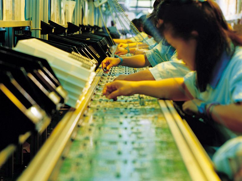
 Now a transparent artwork showing the pattern of the PCB's pads and tracks is placed over the photosensitive copper-clad laminate, and is then exposed to ultraviolet light. Ultraviolet is used rather than visible light so the board can be handled safely in daylight.
 For a six-layer board, the stack would comprise: prepreg / core / prepreg / core / prepreg. This means that the final result will be: fibreglass / copper / fibreglass / copper / fibreglass / copper / fibreglass / copper / fibreglass.
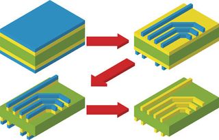

 Here, a different type of artwork is used so that the photo-resist remains in those areas that don't correspond to the pads and tracks of the finished board. Now the electro-plating will only increase the thickness of the copper on the areas without the insulating photo-resist.
 The tackiness of the solder paste holds the components in place, but they're not fixed securely and there isn't a proper electrical connection.
 The board then enters a wave soldering machine. This contains a tank of molten solder that's pumped across a submerged edge, causing a raised wave of solder. As the board progresses through this apparatus, each part of the bottom side of the board comes into contact with the solder wave. The solder adheres to the board wherever it's free of solder resist, thereby making mechanical and electrical connections between the component leads and the pads.
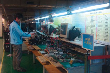 This is mostly an automated process, although humans do still have a part in the process for areas like audio circuitry. All this is followed up with a 'burn-in' test, which involves running diagnostic software on the motherboard for a protracted time while it's subjected to high temperatures and temperature cycles.
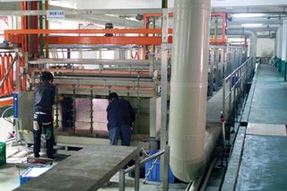
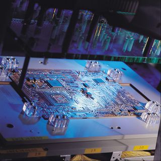

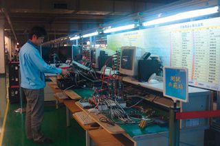
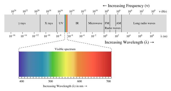
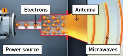
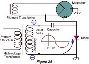
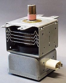
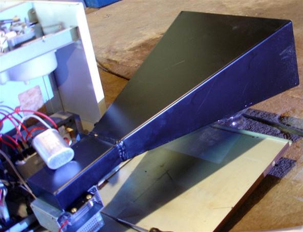
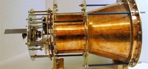


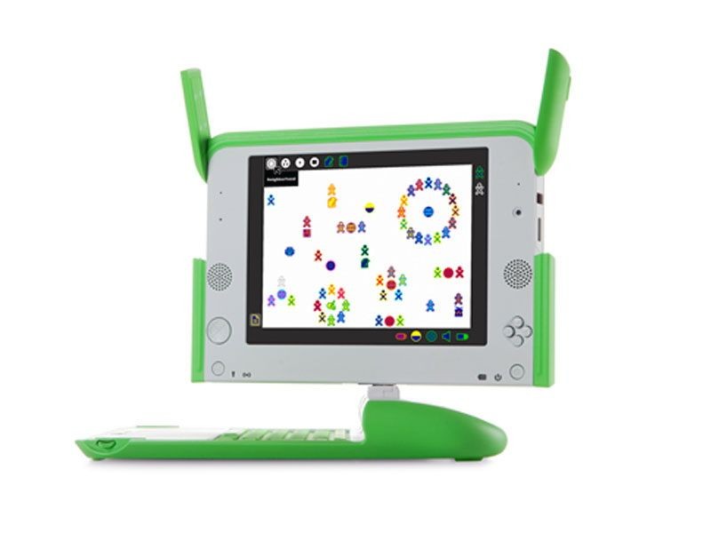
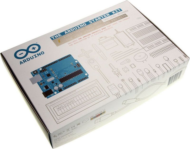
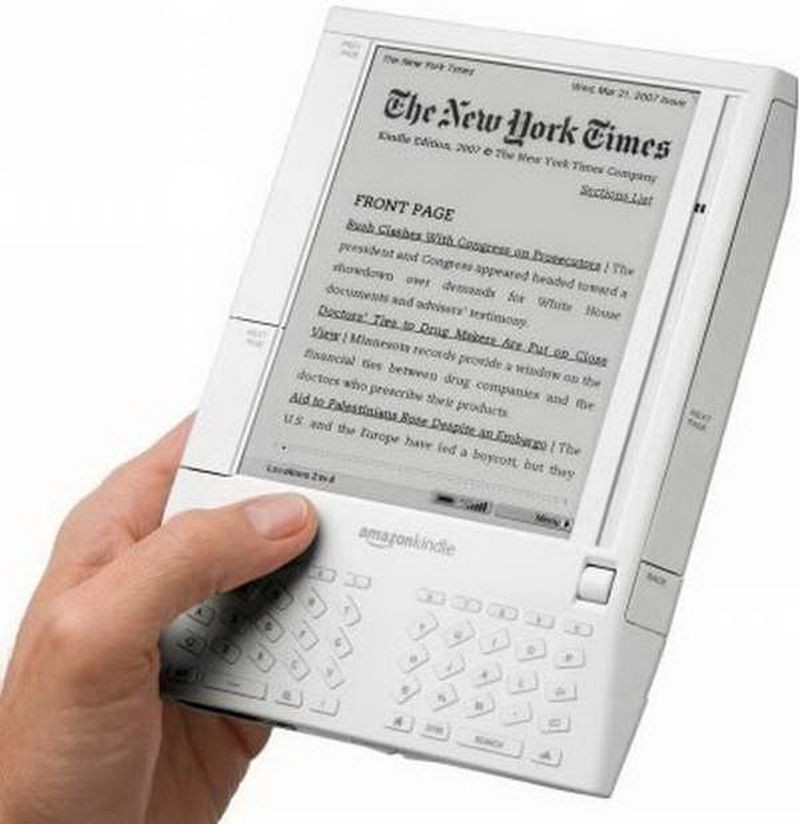


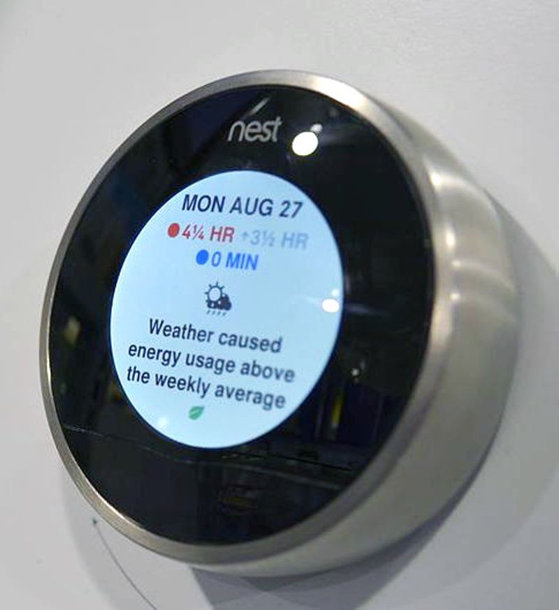


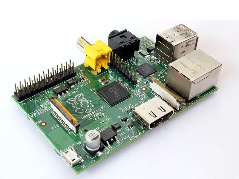


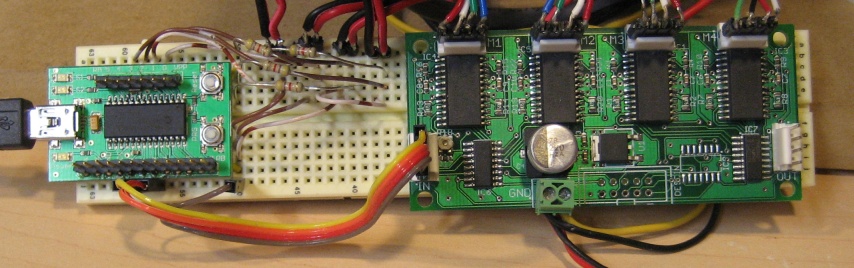


 ,
, 
 Open the picture to see the layers.


 This is a device which sorts the inputs, putting 1's at the bottom and 0's at the top. In effect counting how many 1s and how many 0s there are. The diagram is designed so that it is easily expandable, as shown in the diagram. The bright squares shows how to expand it, and also where the in- and outputs are.


 Some mechanism components only perform an action when initially activated (command blocks execute a command, droppers and dispensers eject an item, note blocks play a sound) and won't do anything again until deactivated and then activated again, while other mechanism components change their state when activated and don't change back until the activation ends (redstone lamps stay on, doors/fence gates/trapdoors stay open, hoppers stay disabled, pistons stay extended, etc.).


.png)


 ,
, 
 Open the picture to see the layers.


 This is a device which sorts the inputs, putting 1's at the bottom and 0's at the top. In effect counting how many 1s and how many 0s there are. The diagram is designed so that it is easily expandable, as shown in the diagram. The bright squares shows how to expand it, and also where the in- and outputs are.


Tidak ada komentar:
Posting Komentar