


Electronics
Capacitors are widely used in electronic circuits for blocking direct current while allowing alternating current to pass. In analog filter networks, they smooth the output of power supplies. In resonant circuits they tune radios to particular frequencies. In electric power transmission systems they stabilize voltage and power flow .
Specific orbital energy
In the gravitational two-body problem, the specific orbital energy (or vis-viva energy) of two orbiting bodies is the constant sum of their mutual potential energy () and their total kinetic energy (), divided by the reduced mass. According to the orbital energy conservation equation (also referred to as vis-viva equation), it does not vary with time:


where
- is the relative orbital speed;
- is the orbital distance between the bodies;
- is the sum of the standard gravitational parameters of the bodies;
- is the specific relative angular momentum in the sense of relative angular momentum divided by the reduced mass;
- is the orbital eccentricity;
- is the semi-major axis.


It is expressed in J/kg = m2·s−2 or MJ/kg = km2·s−2. For an elliptic orbit the specific orbital energy is the negative of the additional energy required to accelerate a mass of one kilogram to escape velocity (parabolic orbit). For a hyperbolic orbit, it is equal to the excess energy compared to that of a parabolic orbit. In this case the specific orbital energy is also referred to as characteristic energy.
Equation forms for different orbits
For an elliptic orbit, the specific orbital energy equation, when combined with conservation of specific angular momentum at one of the orbit's apsides, simplifies to:

where
- is the standard gravitational parameter;
- is semi-major axis of the orbit.

Proof:
-
- For an elliptic orbit with specific angular momentum h given by

-
- we use the general form of the specific orbital energy equation,

-
- with the relation that the relative velocity at periapsis is

-
- Thus our specific orbital energy equation becomes
![\epsilon ={\mu \over {a}}{\left[{(1-e^{2}) \over {{2(1-e)}}^{2}}-{1 \over {(1-e)}}\right]}={\mu \over {a}}{\left[{{(1-e)(1+e)} \over {{2(1-e)}}^{2}}-{1 \over {(1-e)}}\right]}={\mu \over {a}}{\left[{(1+e) \over {{2(1-e)}}}-{2 \over {2(1-e)}}\right]}={\mu \over {a}}{\left[{{e-1} \over {2(1-e)}}\right]}\,\!](https://wikimedia.org/api/rest_v1/media/math/render/svg/76e059f92326ab890f1e90d3550877c4d35ea50e)
-
- and finally with the last simplification we obtain:

For a parabolic orbit this equation simplifies to

For a hyperbolic trajectory this specific orbital energy is either given by

or the same as for an ellipse, depending on the convention for the sign of a.
In this case the specific orbital energy is also referred to as characteristic energy (or ) and is equal to the excess specific energy compared to that for a parabolic orbit.

It is related to the hyperbolic excess velocity (the orbital velocity at infinity) by


It is relevant for interplanetary missions.
Thus, if orbital position vector () and orbital velocity vector () are known at one position, and is known, then the energy can be computed and from that, for any other position, the orbital speed.


Rate of change
For an elliptic orbit the rate of change of the specific orbital energy with respect to a change in the semi-major axis is

where
- is the standard gravitational parameter;
- is semi-major axis of the orbit.
In the case of circular orbits, this rate is one half of the gravity at the orbit. This corresponds to the fact that for such orbits the total energy is one half of the potential energy, because the kinetic energy is minus one half of the potential energy.
Additional energy
If the central body has radius R, then the additional energy of an elliptic orbit compared to being stationary at the surface is

- For the Earth and a just little more than this is ; the quantity is the height the ellipse extends above the surface, plus the periapsis distance (the distance the ellipse extends beyond the center of the Earth); the latter times g is the kinetic energy of the horizontal component of the velocity.


Examples
ISS
The International Space Station has an orbital period of 91.74 minutes (5.5 ks), hence the semi-major axis is 6,738 km.
The energy is −29.6 MJ/kg: the potential energy is −59.2 MJ/kg, and the kinetic energy 29.6 MJ/kg. Compare with the potential energy at the surface, which is −62.6 MJ/kg. The extra potential energy is 3.4 MJ/kg, the total extra energy is 33.0 MJ/kg. The average speed is 7.7 km/s, the net delta-v to reach this orbit is 8.1 km/s (the actual delta-v is typically 1.5–2 km/s more for atmospheric drag and gravity drag).
The increase per meter would be 4.4 J/kg; this rate corresponds to one half of the local gravity of 8.8 m/s².
For an altitude of 100 km (radius is 6471 km):
The energy is −30.8 MJ/kg: the potential energy is −61.6 MJ/kg, and the kinetic energy 30.8 MJ/kg. Compare with the potential energy at the surface, which is −62.6 MJ/kg. The extra potential energy is 1.0 MJ/kg, the total extra energy is 31.8 MJ/kg.
The increase per meter would be 4.8 J/kg; this rate corresponds to one half of the local gravity of 9.5 m/s². The speed is 7.8 km/s, the net delta-v to reach this orbit is 8.0 km/s.
Taking into account the rotation of the Earth, the delta-v is up to 0.46 km/s less (starting at the equator and going east) or more (if going west).
Voyager 1
For Voyager 1, with respect to the Sun:
- = 132,712,440,018 km3s−2 is the standard gravitational parameter of the Sun
- r = 17 billion kilometers
- v = 17.1 km/s

Hence:
- 146 km2s−2 − 8 km2s−2 = 138 km2s−2

Thus the hyperbolic excess velocity (the theoretical orbital velocity at infinity) is given by
- 16.6 km/s

However, Voyager 1 does not have enough velocity to leave the Milky Way. The computed speed applies far away from the Sun, but at such a position that the potential energy with respect to the Milky Way as a whole has changed negligibly, and only if there is no strong interaction with celestial bodies other than the Sun.
Applying thrust
Assume:
- a is the acceleration due to thrust (the time-rate at which delta-v is spent)
- g is the gravitational field strength
- v is the velocity of the rocket
Then the time-rate of change of the specific energy of the rocket is : an amount for the kinetic energy and an amount for the potential energy.


The change of the specific energy of the rocket per unit change of delta-v is

which is |v| times the cosine of the angle between v and a.
Thus, when applying delta-v to increase specific orbital energy, this is done most efficiently if a is applied in the direction of v, and when |v| is large. If the angle between v and g is obtuse, for example in a launch and in a transfer to a higher orbit, this means applying the delta-v as early as possible and at full capacity. See also gravity drag. When passing by a celestial body it means applying thrust when nearest to the body. When gradually making an elliptic orbit larger, it means applying thrust each time when near the periapsis.
When applying delta-v to decrease specific orbital energy, this is done most efficiently if a is applied in the direction opposite to that of v, and again when |v| is large. If the angle between v and g is acute, for example in a landing (on a celestial body without atmosphere) and in a transfer to a circular orbit around a celestial body when arriving from outside, this means applying the delta-v as late as possible. When passing by a planet it means applying thrust when nearest to the planet. When gradually making an elliptic orbit smaller, it means applying thrust each time when near the periapsis.
If a is in the direction of v:

Tangential velocities at altitude
| Orbit | Center-to-center distance | Altitude above the Earth's surface | Speed | Orbital period | Specific orbital energy |
|---|---|---|---|---|---|
| Standing on Earth's surface at the equator (for comparison – not an orbit) | 6,378 km | 0 km | 465.1 m/s (1,674 km/h or 1,040 mph) | 23 h 56 min | −62.6 MJ/kg |
| Orbiting at Earth's surface (equator) | 6,378 km | 0 km | 7.9 km/s (28,440 km/h or 17,672 mph) | 1 h 24 min 18 sec | −31.2 MJ/kg |
| Low Earth orbit | 6,600–8,400 km | 200–2,000 km | circular orbit: 7.8–6.9 km/s (17,450–14,430 mph) respectively elliptic orbit: 6.5–8.2 km/s respectively | 1 h 29 min – 2 h 8 min | −29.8 MJ/kg |
| Molniya orbit | 6,900–46,300 km | 500–39,900 km | 1.5–10.0 km/s (3,335–22,370 mph) respectively | 11 h 58 min | −4.7 MJ/kg |
| Geostationary | 42,000 km | 35,786 km | 3.1 km/s (6,935 mph) | 23 h 56 min | −4.6 MJ/kg |
| Orbit of the Moon | 363,000–406,000 km | 357,000–399,000 km | 0.97–1.08 km/s (2,170–2,416 mph) respectively | 27.3 days | −0.5 MJ/kg |
Energy storage is the capture of energy produced at one time for use at a later time. A device that stores energy is sometimes called an accumulator or battery. Energy comes in multiple forms including radiation, chemical, gravitational potential, electrical potential, electricity, elevated temperature, latent heat and kinetic. Energy storage involves converting energy from forms that are difficult to store to more conveniently or economically store able forms. Bulk energy storage is currently dominated by hydroelectric dams, both conventional as well as pumped.
Some technologies provide short-term energy storage, while others can endure for much longer.
A wind-up clock stores potential energy (in this case mechanical, in the spring tension), a rechargeable battery stores readily convertible chemical energy to operate a mobile phone, and a hydroelectric dam stores energy in a reservoir as gravitational potential energy. Fossil fuels such as coal and gasoline store ancient energy derived from sunlight by organisms that later died, became buried and over time were then converted into these fuels. Food (which is made by the same process as fossil fuels) is a form of energy stored in chemical form.
Ice storage tanks store ice frozen by cheaper energy at night to meet peak daytime demand for cooling. The energy isn't stored directly, but the work-product of consuming energy (pumping away heat) is stored, having the equivalent effect on daytime consumption.
Flow battery
A flow battery operates by passing a solution over a membrane where ions are exchanged to charge/discharge the cell. Cell voltage is chemically determined by the Nernst equation and ranges, in practical applications, from 1.0 to 2.2 V. Its storage capacity is a function of the volume of the tanks holding the solution.
A flow battery is technically akin both to a fuel cell and an electrochemical accumulator cell. Commercial applications are for long half-cycle storage such as backup grid power.
Supercapacitor

Supercapacitors, also called electric double-layer capacitors (EDLC) or ultracapacitors, are generic terms for a family of electrochemical capacitors . that do not have conventional solid dielectrics. Capacitance is determined by two storage principles, double-layer capacitance and pseudocapacitance.
Supercapacitors bridge the gap between conventional capacitors and rechargeable batteries. They store the most energy per unit volume or mass (energy density) among capacitors. They support up to 10,000 farads/1.2 volt, up to 10,000 times that of electrolytic capacitors, but deliver or accept less than half as much power per unit time (power density).
While supercapacitors have specific energy and energy densities that are approximately 10% of batteries, their power density is generally 10 to 100 times greater. This results in much shorter charge/discharge cycles. Additionally, they will tolerate many more charge and discharge cycles than batteries.
Supercapacitors support a broad spectrum of applications, including:
- Low supply current for memory backup in static random-access memory (SRAM)
- Power for cars, buses, trains, cranes and elevators, including energy recovery from braking, short-term energy storage and burst-mode power delivery
UltraBattery
The UltraBattery is a hybrid lead-acid cell and carbon-based ultracapacitor (or supercapacitor) invented by Australia’s national research body, the Commonwealth Scientific and Industrial Research Organisation (CSIRO). The lead-acid cell and ultracapacitor share the sulfuric acid electrolyte and both are packaged into the same physical unit. The UltraBattery can be manufactured with similar physical and electrical characteristics to conventional lead-acid batteries making it possible to cost-effectively replace many lead-acid applications.
The UltraBattery tolerates high charge and discharge levels and endures large numbers of cycles, outperforming previous lead-acid cells by more than an order of magnitude. In hybrid-electric vehicle tests, millions of cycles have been achieved. The Ultra Battery is also highly tolerant to the effects of sulfation compared with traditional lead-acid cells. This means it can operate continuously in partial state of charge whereas traditional lead-acid batteries are generally held at full charge between discharge events. It is generally electrically inefficient to fully charge a lead-acid battery so by decreasing time spent in the top region of charge the Ultra Battery achieves high efficiencies, typically between 85 and 95% DC-DC.
The Ultra Battery can work across a wide range of applications. The constant cycling and fast charging and discharging necessary for applications such as grid regulation and leveling and electric vehicles can damage chemical batteries, but are well handled by the ultra capacitive qualities of Ultra Battery technology. The technology has been installed in Australia and the US on the megawatt scale, performing frequency regulation and renewable smoothing applications .
Electrical methods
Capacitor

A capacitor (originally known as a 'condenser') is a passive two-terminal electrical component used to store energy electrostatically. Practical capacitors vary widely, but all contain at least two electrical conductors (plates) separated by a dielectric (i.e., insulator). A capacitor can store electric energy when disconnected from its charging circuit, so it can be used like a temporary battery, or like other types of rechargeable energy storage system.[62] Capacitors are commonly used in electronic devices to maintain power supply while batteries change. (This prevents loss of information in volatile memory.) Conventional capacitors provide less than 360 joules per kilogram, while a conventional alkaline battery has a density of 590 kJ/kg.
Capacitors store energy in an electrostatic field between their plates. Given a potential difference across the conductors (e.g., when a capacitor is attached across a battery), an electric field develops across the dielectric, causing positive charge (+Q) to collect on one plate and negative charge (-Q) to collect on the other plate. If a battery is attached to a capacitor for a sufficient amount of time, no current can flow through the capacitor. However, if an accelerating or alternating voltage is applied across the leads of the capacitor, a displacement current can flow. Besides capacitor plates, charge can also be stored in a dielectric layer.
Capacitance is greater given a narrower separation between conductors and when the conductors have a larger surface area. In practice, the dielectric between the plates emits a small amount of leakage current and has an electric field strength limit, known as the breakdown voltage. However, the effect of recovery of a dielectric after a high-voltage breakdown holds promise for a new generation of self-healing capacitors. The conductors and leads introduce undesired inductance and resistance.
Research is assessing the quantum effects of nanoscale capacitors for digital quantum batteries.
Superconducting magnetics
Superconducting magnetic energy storage (SMES) systems store energy in a magnetic field created by the flow of direct current in a superconducting coil that has been cooled to a temperature below its superconducting critical temperature. A typical SMES system includes a superconducting coil, power conditioning system and refrigerator. Once the superconducting coil is charged, the current does not decay and the magnetic energy can be stored indefinitely.
The stored energy can be released to the network by discharging the coil. The associated inverter/rectifier accounts for about 2–3% energy loss in each direction. SMES loses the least amount of electricity in the energy storage process compared to other methods of storing energy. SMES systems offer round-trip efficiency greater than 95%.
Due to the energy requirements of refrigeration and the cost of superconducting wire, SMES is used for short duration storage such as improving power quality. It also has applications in grid balancing.[69]
Interseasonal thermal storage
Seasonal thermal energy storage (STES) allows heat or cold to be used months after it was collected from waste energy or natural sources. The material can be stored in contained aquifers, clusters of boreholes in geological substrates such as sand or crystalline bedrock, in lined pits filled with gravel and water, or water-filled mines.
Flow Battery Energy Storage (FBES)
A flow battery stores energy in two soluble redox couples contained in external liquid electrolyte tanks. These electrolytes can be pumped from the tanks to the cell stack which consists of two electrolyte flow compartments separated by ion selective membranes. The operation is based on reduction-oxidation reactions of the electrolyte solutions. During the charging phase, one electrolyte is oxidized at the anode and another electrolyte is reduced at the cathode, and the electrical energy is converted to the electrolyte chemical energy. The above process is reversed during the discharging phase.
Flow batteries can be classified into the categories of redox flow batteries and hybrid flow batteries, depending on whether all electroactive components can be dissolved in the electrolyte. Fig. * shows a schematic diagram of a vanadium redox flow battery system. A crucial advantage of FBES is that the power of a FBES system is independent of its storage capacity. The power of the FBES system is determined by the size of the electrodes and the number of cells in the stack; whereas the storage capacity is determined by the concentration and the amount of electrolyte . Also, the very small self-discharge is an inherent strength of the FBES system due to the electrolytes being stored in separate sealed tanks . Drawbacks of flow batteries include low performance resulting from non-uniform pressure drops and the reactant mass transfer limitation, relatively high manufacturing costs and more complicated system requirements compared to traditional batteries

Capacitor and supercapacitor
A capacitor is composed of at least two electrical conductors (normally made of metal foils) separated by a thin layer of insulator (normally made of ceramic, glass or a plastic film). When a capacitor is charged, energy is stored in the dielectric material in an electrostatic field . Its maximum operating voltage is dependent on the breakdown characteristics of the dielectric material. Capacitors are appropriate for storing small quantities of electrical energy and conducting a varying voltage; they have a higher power density and shorter charging time compared to conventional batteries . However, they have limited capacity, relatively low energy density and high energy dissipation due to the high self-discharge losses . According to these characteristics, capacitors can be used for some power quality applications, such as high voltage power correction, smoothing the output of power supplies, bridging and energy recovery in mass transit systems.
Supercapacitors, also named electric double-layer capacitors or ultra capacitors, contain two conductor electrodes, an electrolyte and a porous membrane separator. Due to their structures, supercapacitors can have both the characteristics of traditional capacitors and electrochemical batteries. The energy is stored in the form of static charge on the surfaces between the electrolyte and the two conductor electrodes. The super capacitors with high-performance are based on nano materials to increase electrode surface area for enhancing the capacitance.

Superconducting Magnetic Energy Storage (SMES)
A typical SMES system is composed of three main components which include: a superconducting coil unit, a power conditioning subsystem, and a refrigeration and vacuum subsystem . The SMES system stores electrical energy in the magnetic field generated by the Direct Current (DC) in the superconducting coil which has been cryogenically cooled to a temperature below its superconducting critical temperature. In general, when current passes through a coil, the electrical energy will be dissipated as heat due to the resistance of the wire; however, if the coil is made from a superconducting material, such as mercury or vanadium, under its superconducting state (normally at a very low temperature), zero resistance occurs and the electrical energy can be stored with almost no losses. One commonly used superconducting material is Niobium–Titanium which has a superconducting critical temperature of 9.2 K . In the discharging phase, the SMES system can release the stored electrical energy back to the Alternating Current (AC) system, by a connected power converter module. The magnitude of stored energy is determined by the self-inductance of coil and the current flowing through it . A simplified structure of a SMES system is illustrated in

Superconducting coils can be classified into two groups: Low Temperature Superconducting (LTS) coils, working at ∼5 K, and High Temperature Superconducting (HTS) coils, working at ∼70 K . The LTS-SMES technology is more mature and commercially available while the HTS-SMES is currently in the development stage. SMES devices in the range of 0.1–10 MW have been used commercially; while SMES systems with 100 MW h could be available in the next decade.
The features of SMES include relatively high power density (up to ∼4000 W/L), fast response time (millisecond level), very quick full discharge time (less than 1 min), high cycle efficiency (∼95–98%) and long lifetime (up to ∼30 years) . In contrast to rechargeable batteries, SMES devices are capable of discharging near to the totality of the stored energy with little degradation after thousands of full cycles. The drawbacks are that they have high capital cost (up to 10,000 $/kW h, 7200 $/kW), high daily self-discharge (10–15%) and a negative environmental impact due to the strong magnetic field . Moreover, the coil is sensitive to small temperature variations which can cause the loss of energy. From the above, SMES is suitable for short-term storage in power and energy system applications and it is expected to have an important role in the increased use of intermittent renewable energy .
Recently, considerable research and development effort has been made: (1) to reduce the costs of superconducting coils and related refrigeration systems; (2) to develop HTS coil materials which are less cryogenically sensitive . Since 2011, Super Power Inc., in partnership with ABB Inc., Brookhaven national laboratory and the Texas center for superconductivity at the University of Houston has been developing an advanced SMES demonstrator 20 kW ultra-high field SMES system with a capacity up to 2 MJ . This demonstration project aims to pave the way of grid-scale SMES technology for the U.S. electric grid operation and for the integration of renewable sources. The University of Bath in the UK continuously focus on SMES technology development and a relevant on-going project funded by the UK EPSRC aims to investigate HTS-SMES as part of hybrid EES systems for renewable energy micro-grids .
3.8. Solar fuels
Solar fuel is a relatively new technology to EES. Approaches to produce solar fuels include: (1) natural photosynthesis; (2) artificial photosynthesis; (3) thermochemical approaches . A number of fuels can be produced by solar energy, such as solar hydrogen, carbon-based fuels, and solar chemical heat pipe . These fuels can be stored and subsequently provide the basis for later electricity generation.
For the first two approaches to produce solar fuels, solar energy is captured via photosynthesis and then stored in chemical bonds, i.e., the sunlight is used to convert water and/or carbon dioxide into oxygen and other materials shows a comparison of natural and artificial photosynthesis. The artificial system for water-splitting catalysts generally relies on scarce elements, e.g., Ruthenium (Ru), Palladium (Pd) and Rhenium (Re) . For example, sunlight can be captured by Ruthenium (Ru) as a catalyst, and electrons moves from the donor (marked as “D”) to the acceptor .

The thermochemical approach uses thermal processes for solar fuels production, which involve the generation of very high temperatures in a closed environment to split water into its constituent parts . Thus this method is more dependent on strong sunlight compared to the other two . After the solar radiant energy is concentrated by heliostats, an endothermic chemical transformation is carried out in a reaction vessel. The reaction produces hydrogen and/or carbon monoxide and/or other materials .
Solar fuel technology is currently at the development stage. The power rating of solar fuels is potentially up to 20 MW and the specific energy estimate is from 800 W h/kg to 100,000 W h/kg . The storage duration can range from a few hours to several months . One drawback of artificial photosynthesis is that the water-splitting catalysts normally depend on scarce, expensive elements . Another disadvantage is that solar fuel facilities need a large area to place devices to concentrate sunlight, especially when using the thermochemical approach to produce solar fuels.
Research in solar fuels has recently undergone substantial advances, making it possible for it to become cost-effective for utility EES applications in the near future. There are on-going research projects in the U.S., the Netherlands, South Korea, Singapore, Japan and China. In the US, there are several organizations focusing on this area, such as Energy Innovation Hub at DoE, the MIT spin-out Sun Catalytix and the Princeton University spin-out Liquid Light. The “Towards BioSolar Cells” research programme has focused on increasing the photosynthetic efficiency and creating solar collectors . Concerning the issue of the reliance on scarce and expensive elements, one important breakthrough in the development of using earth-abundant, relatively cheap catalysts (e.g. cobalt and phosphate) and silicon-based semiconductors for the water-splitting process has been recently reported by the Nocera’s team from MIT . Asia’s pioneering solar fuel research laboratory at Nanyang Technological University of Singapore has also made effort on the investigation of affordable approaches to extract large amounts of hydrogen from water using sunlight for engineering applications
Hydrogen storage and fuel cell
Hydrogen energy storage systems use two separate processes for storing energy and producing electricity . The use of a water electrolysis unit is a common way to produce hydrogen which can be stored in high pressure containers and/or transmitted by pipelines for later use When using the stored hydrogen for electricity generation, the fuel cell (also known as regenerative fuel cell) is adopted, which is the key technology in hydrogen EES.

Fuel cells can convert chemical energy in hydrogen (or hydrogen-rich fuel) and oxygen (from air) to electricity . The overall reaction is: 2H2 + O2 → 2H2O + energy . Electrical and heat energy are released during the process . Depending on the choice of fuel and electrolyte, there are six major groups of fuel cells, which are: Alkaline Fuel Cell (AFC), Phosphoric Acid Fuel Cell (PAFC), Solid Oxide Fuel Cell (SOFC), Molten Carbonate Fuel Cell (MCFC), Proton Exchange Membrane Fuel Cell (PEMFC) and Direct Methanol Fuel Cell (DMFC)
In general, the electricity generation by using fuel cells is quieter, produces less pollution and is more efficient than the fossil fuel combustion approach . Other features include easy scaling (potential from 1 kW to hundreds of MW) and compact design . Fuel cell systems combined with hydrogen production and storage can provide stationary or distributed power (primary electrical power, heating/cooling or backup power) and transportation power (potentially replacing fossil fuels for vehicles) . Such hydrogen EES systems can offer capacity and power independence in energy production, storage and usage, due to the separate processes. It should be noted that the disposal of exhaust fuel cells must consider degradation and recycling while toxic metals are used as electrodes or catalysts. Many of the relevant aspects and approaches have been under investigation , . For instance, palladium in catalysts of fuel cells can be reprocessed into other products in theory .
Currently, hydrogen EES with fuel cell technology is in the development and demonstration stage. Stationary power applications are relatively mature. In 2012 nearly 80% of total investment in the global fuel cell industry was made by the U.S. companies . Cost reduction and durability verification/improvement are essential to deploy this technology in large-scale EES applications . Some research or demonstration projects are in place and on-going across the world. The world’s first utility-scale test of a stand-alone renewable energy system integrated with hydrogen storage and fuel cells was installed in Norway, which delivered power with required quality and high reliability . One of the world’s largest biogas fuel cell power plants was launched in 2012 in California (2.8 MW), which converts biogas into electricity and usable high-quality heat . In 2013, the US Naval Air Warfare Center Weapons Division in California successfully tested a novel 5 kW trailer-mounted regenerative fuel cell system to use solar power to produce hydrogen with fuel cells . Since 2013, McPhy and Enertrag AG in Germany have worked jointly to develop economic wind-hydrogen solutions for EES and for transportation fuel cell applications . Currently, the on-going hydrogen storage and fuel cell relevant projects include IdealHy (the Netherlands), RE4CELL (Spain), Sapphire (Norway), SmartCat (France), etc.
XO__XO XXX components of electronics components switch mode power supply
Critical Components Behind Switch-mode Power Supplies ( Power Semiconductor )
passive components in the input circuit of a power supply is to protect the electronic device from overcurrent and overvoltage and ensure electromagnetic compatibility—especially important considerations in today’s portable applications where long battery life is a necessity. The choice of the components used in switch-mode power supplies (SMPS) is extremely important, as their impact on performance is often not considered. These components—such as resistors, capacitors and inductors—are called upon to deal with heat, size, output power and device price tag.
Switch-mode power supplies switch on and off at high frequency, providing electric energy transfer from capacitors and inductors. SMPS are smaller and feature a lighter package and reduced manufacturing costs.
While there are many components involved in SMPS, a handful of critical devices include:
1. Capacitors
Capacitors perform energy storage, filtering, compensation and soft-start programming. The overriding loss for capacitors in SMPS applications is based on effective series resistance (ESR). ESR results from the physical construction of a capacitor, the resistance of internal interconnects, and even the behavior of the material used as an insulator between capacitor plates. Many capacitors are particularly sensitive to heat and a function of ESR is to dissipate heat in the presence of a current flow into or out of a capacitor. The ESR of a capacitor is typically the most important specification when selecting capacitors for SMPS applications—even more important than the component’s basic capacitance rating.
Capacitors represent the key components of the DC link. They smooth the rectifier ripple voltage and stabilize the DC link voltage. While all rectifiers produce an output voltage that has ripple superimposed on the DC, it varies in magnitude, waveform and frequency depending on the rectifiers. The downside of ripple includes possible reduced productivity or process equipment life, interference with process instrumentation, and electromagnetic coupling with nearby structures, resulting in heating of the structures and increased losses.
DC link capacitors expose the rectifier and power line to extremely high input currents at the moment of turn-on, potentially destroying the rectifier diode or causing the power fuse to blow. This can be avoided by using negative temperature coefficient (NTC) thermistors as inrush current limiters (ICL), for a gentle power up. When NTC ICLs are sufficiently heated by the current flow, their resistance drops to a negligible value. The B57*S series of EPCOS NTC thermistors offers a corresponding ICL for each required current strength.
EPCOS aluminum electrolytic capacitors are particularly suitable for this job based on their high CV value; they allow today’s compact power supplies to be easily implemented. The capacitors are distinguished by a very high ripple current capability, combined with low ESR and ESL values, leading to lower intrinsic heating. Depending on the required output and voltage of the link circuit, radial versions or snap-in types with two or four pins are used. The capacitors cover a voltage range from 10 V DC to 600 V DC and maximum temperatures of 85° C to 140° C.
In two EPCOS aluminum electrolytic capacitors with screw terminals (B43700* and B43720*), the permissible rated voltage increased from 550 V DC to 600 V DC. Covering a capacitance range from 680 µF to 6800 µF, the highly compact components are designed for temperatures up to 85° C. A new snap-in series (B43541*) for temperatures up to 85° C, offers a rated voltage of 600 V DC instead of the previous 550 V DC, and features capacitance values of between 47 µF and 270 µF.
Among the newcomers to the range are types with a higher-rated voltage for temperatures up to 105° C. Screw-terminal types are rated at 500 V DC instead of the previous 450 V DC, and the rating of the snap-in types increased from 500 V DC to 550 V DC. The benefit to developers is that they need to connect fewer series capacitors in the link circuit, which reduces costs and mounting space.
Alternatively, EPCOS MKP film capacitors can also be used to stabilize the DC link. The B3267* high-power series and the B3277* high-density series are designed for voltages from 450 V DC to 1300 V DC and cover a capacitance range from 0.47 µF to 110 µF. As with all EPCOS film capacitors, they are distinguished by a very long operating life and are self-healing. Dielectric breakdowns caused by over-voltages lead to local vaporization of the metallization, yet the capacitor remains fully functional.
 EPCOS and TDK components in the input circuit of a power supply protect the electronic device against overcurrent and overvoltage, assuring EMC.
2. PTC Thermistors
In comparison to the NTC thermistors previously mentioned, positive temperature coefficient (PTC) thermistors provide protection from current surges, such as those that occur as a result of a short circuit. At excessive currents, these components heat up and acquire a high resistance. As with ICLs, they are inserted directly into the current path of the power input. The B5910*J series spans commonly used current levels and are available in leaded or packaged versions.
3. Varistors
Varistors (variable resistors), commonly referred to as Metal Oxide Varistors (MOVs), are ceramic-based components used to protect susceptible circuitry against damaging overvoltage conditions. Varistors are voltage-dependent resistors whose resistance decreases with increasing voltage. Connected in parallel with the electronic device, or circuit that is to be protected, a varistor forms a low-resistance shunt when voltage increases. Common overvoltage sources include lightning, inductive load switching and electrostatic discharge (ESD).
EPCOS offers an extensive range of varistors including leaded and SMD equivalents, ThermoFuse types and Multilayer SMDs.
- Leaded and SMD equivalents span voltages ranging from 11 to 1000 Vac, surge current ratings from 100A thru 100kA, energy ratings from .3 thru 6000 joules, as well as new125° high-temperature types
- ThermoFuse varistors range from 130 to 1000 Vac and surge current ratings to 10,000A . A varistor disc in the series with a thermally coupled fuse is packaged in a plastic housing. If the varistor overheats, the thermal fuse activates, disconnecting the varistor from the circuit.
- Multilayer SMD types in case sizes 0201 thru 2220 feature voltages ranging from 4 thru 60 Vac with surge current ratings up to 1200A
4. EMC and Transient Protection
The ability of a system to function in an electromagnetic environment without introducing electromagnetic disturbances that may interfere with other electrical products in the same environment is called electromagnetic compatibility (EMC). EMC and transient protection is delivered via a broad range of EPCOS X- and Y-capacitors and common-mode chokes. For example, the electromagnetic interference (EMI) capacitors of the B3292*, B3202*, B3291* and B81123 series are designed for voltages of 250 V AC to 350 V AC.
In addition, EPCOS also offers a broad range of double, triple and quadruple common-mode chokes with the B827* series, with voltages that extend from 250 V AC to 690 V AC and permissible current-handling capacities from 0.25A to 200A.
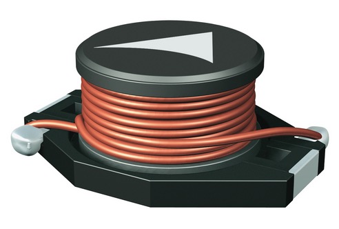
5. High-performance and Compact Inductors
Inductors are magnetic energy-storage elements that consist of a wire coil wound around a ferromagnetic core. Current that flows through the inductor induces a magnetic field in the core. This field is the mechanism for energy storage. Current in an inductor cannot change instantaneously; when a voltage is applied across an inductor, the current will ramp.
When the switch closes, the full voltage appears across the inductor. When the switch is open, the current in the inductor will ramp down at the same rate and a large voltage is generated as the magnetic field collapses. The magnetic field is the energy-storage mechanism.
Two main core materials are used in inductors for SMPS—powdered iron and solid ferrite. A powdered iron core has air gaps within the material, giving a soft saturation curve. These are for applications that need large, instantaneous current. In comparison, ferrite core inductors saturate faster but are lower cost and have lower core losses.
To reach various voltage levels at the SMPS output, MOSFET-switched power transformers of the EPCOS B78* series are required. They are offered in the most varied core shapes, as well as in SMD or plated through hole (PTH) versions. Despite their compact dimensions, outputs of up to 200 W can be realized per transformer. Versions with several outputs are available. The new chokes and transformers of the EPCOS e-mobility platform represent a special highlight. They were developed specifically for on-board chargers and are characterized, apart from their compact dimensions, especially by low losses.
 Power inductors are used in SMPS applications with high requirements for temperature range and reliability.
To smooth the output voltages after rectification, EPCOS SMT inductors must be present in the current path; the EPCOS series B8246*, B8247* or B8255* are suitable for this purpose. The range covers types with current-handling capabilities from 0.11 A to 71 A in shielded and unshielded versions. Thanks to the flat-wire helical windings of the high-current versions, this produces a very high copper fill factor so that these components have a low space requirement despite their high performance. TDK inductors are ideal for this purpose. Single-ended aluminum electrolytic capacitors of the B41* series or film capacitors are recommended for smoothing the voltage path.
EPCOS current sensors are indispensable for exact regulation of SMPS. The B82801* series specifically targets this purpose. The sensors are available with transformation ratios of 1:20 to 1:125 and designed for currents from 7 to 40 A.
SMPS can be used in computers, instrumentation, laser and medical applications. They are ideal for use across a wide range of power classes from a few watts when charging a phone, to kilowatts in high-performance industrial power supplies. Design engineers must carefully select such critical components in order to deliver higher performance and greater reliability to the end design.
Components of SWITCH MODE POWER SUPPLY (SMPS) Most of the components used in SWITCH MODE POWER SUPPLY (SMPS) can be easily identified. However, some components are difficult to identify. Some components are designed especially for a particular model. The different components of SWITCH MODE POWER SUPPLY (SMPS) are:
Most of the components used in SWITCH MODE POWER SUPPLY (SMPS) can be easily identified. However, some components are difficult to identify. Some components are designed especially for a particular model. The different components of SWITCH MODE POWER SUPPLY (SMPS) are:
Switch Mode (chopper) Transistors and other Semiconductors.
A transistor is small and fast semiconductor used for amplification and voltage stabilization.
Bipolar Power Transistors (often BU or 2SC/2SD numbers.) High voltage power transistors, which are used as the main switch mode transistor.
Diodes and Rectifiers - AC line rectifier uses a combination of 2 or 4 diodes. High efficiency diodes are used to rectify output voltages. These diodes look like normal axial lead diodes. They can be combined in pairs inside TO220 type packages. To troubleshoot SWITCH MODE POWER SUPPLY (SMPS) problems, test for shorted and open junctions.
Capacitors (filter and bypass) in an SWITCH MODE POWER SUPPLY (SMPS)
Filter Capacitors - Used to filter the rectified AC line input voltage and various outputs of the power supply.
Bypass Capacitors - These are green colored, high quality plastic dipped or rectangular molded capacitors part of RFI filter. They are placed at output section and seldom fail.
Resistors - Test for proper value with the help of multimeter. While measuring the resistor in-circuit, if the value is higher than normal value, then resistor is bad.
Startup Resistors - They are high value (100K) medium wattage resistors. Test for open circuit results in dead supply without blown fuses or fusable resistors.

Pixabay
Flameproof or Fusable Resistors - They are rectangular ceramic blocks which are blue or gray in color. They function as fuses; hence they cannot be replaced with higher wattage types. Test for open circuits.
WTC Resistors (thermistors) - Negative Temperature Coefficient resistors act as inrush surge limiters. There may be one or two of these in series with the AC input. These often look like fat black disk capacitors.
Transformers and Inductors required in a SWITCH MODE POWER SUPPLY (SMPS)
High Frequency Transformers - They consist of the switch Mode power transformer and feedback transformer. They provide line isolation and generate multiple output voltage. They rarely cause problems and can be tested for open circuit. Some supplies use small Transformers for feedback instead of optoisolators. Optoisolator is used to isolate the input line with the rest of the section.
Inductors - Output inductors rarely fail and they can be tested for open circuit. Replace the faulty inductor if found.
Coupled Inductors - They are used as a part of Pi type RFI filter which is placed in the AC input circuit. The windings of inductor are in series with AC line. They look like small transformer. They are very reliable and help to reduce noise and spikes. They can be tested for open circuit.
Reliable protection and stabilization

TDK offers developers of power supplies one-stop shopping for passive components: The extremely broad range, especially of EPCOS components, covers all types of powerful DC link capacitors. They are complemented by an extensive range of transformers, chokes, protection devices and EMC components, and more.
Very few electrical devices are still powered by AC voltage from the power line. Whether in communications and information technology, consumer electronics, industrial electronics or lighting, power supplies are omnipresent in a large variety of topologies.
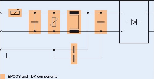
Power supply technology encompasses converters for photovoltaic and wind power plants and frequency converters for industrial drives as well as switch-mode power supplies in a very wide range of power classes. The latter extends from a few watts for mobile phone chargers up to the kilowatt range for high-performance industrial power supplies. Figure 1 shows a typical layout of the input circuit of switch-mode power supplies (SMPS) with all passive components upstream of the rectifier.
| Figure 1: Input circuit layout of a switch-mode power supply | |
|

Safe from current surges
DC link capacitors expose the rectifier and power line to extremely high input currents at the moment of turn-on. In extreme cases, this can lead to the destruction of the rectifier diode or cause the power fuse to blow.
This can be avoided by the use of NTC thermistors as inrush current limiters (ICL), which ensure a gentle power-up. These thermistors have a relatively high resistance at the moment of turn-on and thus limit the inrush current. Only when they have been sufficiently heated by the current flow does their resistance drop to a negligible value. The B57*S series of EPCOS NTC thermistors offers a corresponding ICL for every required current strength.
During operation, PTC thermistors assure protection from current surges, such as during a short circuit. At excessive currents, these components heat up and acquire a high resistance. Just like the ICLs, they are inserted directly into the current path of the power input. The B5910*J series covers the commonly used current levels. These components are available in leaded or packaged versions. Figure 2 shows NTC and PTC thermistors for overcurrent protection and a varistor of the ETFV series, a component that combines multiple protection functions.
| Figure 2: Ceramic protection devices | |
|

Decentralized power generation, especially via wind power and solar plants, increases the risk of voltage fluctuations and dangerous overvoltages. Safe operation of power supplies can be assured by using the EPCOS varistors which make TDK the world market leader in overvoltage protection devices. These ceramic components are continuously being further developed and improved. Thus, types that can handle multiple high-voltage pulses are now available. The varistors of the ETFV series feature a special highlight (Figure 2 right). They are equipped with an integrated thermal fuse that disconnects the component in the event of overload. These components also offer a monitor output via which a malfunction can be signaled. Thanks to their heat resistance and flame-retardant design, these varistors satisfy UL 94 V-0 specifications. Moreover, they are qualified to UL 1449 3rd edition, UL 60691 and IEC 6 0950-1 Annex Q. The ETFV varistors can be connected via circuit board clamps, which significantly simplifies maintenance. In addition to many variants of monolithic varistors with diverse connection configurations and power ratings, SMD multilayer varistors are also very well suited to protect the control electronics of power supplies.
EMC – an absolute must
For EMC and transient protection, EPCOS offers one of the broadest ranges of X- and Y-capacitors and common-mode chokes worldwide. The EMI capacitors of the B3292*, B3202*, B3291* and B81123 series are designed for voltages of 250 V AC to 330 V AC. These components have the corresponding approvals to UL1414, UL1283, CSA C22.2 and EN 60384-14.
EPCOS offers a wide range of double, triple and quad common-mode chokes with the B827* series. Their voltages extend from 250 V AC to 690 V AC, and their permissible current handling capacities from 0.25 A to 200 A.
To achieve maximum efficiency with a simultaneously low power-line load via a large conduction angle, a PFC boost stage is connected immediately after the rectifier. EPCOS inductors are ideally suited for this purpose. They offer a wide range of current capabilities and are available as both leaded and SMD components.
| Figure 3: EPCOS EMC components for power supplies | |
|

| Figure 4: Circuit diagram of an SMPS with DC link circuit, converter and output filtering | |
|

Capacitors for the DC link
The key components of the DC link are the capacitors. They smooth the rectifier ripple voltage and thus stabilize the DC link voltage. EPCOS aluminum electrolytic capacitors are suitable for this purpose. With their high CV values, they allow highly compact power supplies to be implemented. EPCOS aluminum electrolytic capacitors are distinguished by a very high ripple current capability and low ESR and ESL values, leading to lower intrinsic heating. Depending on the required output and voltage of the link circuit, radial versions or snap-in types with 2 or 4 pins are used here. The capacitors cover a voltage range from 10 V DC to 600 V DC and are designed for maximum temperatures of 85 °C to 140 °C.
In two newly developed series of EPCOS aluminum electrolytic capacitors with screw terminals (B43700* and B43720*), the permissible rated voltage has now been increased from 550 V DC to 600 V DC (Figure 5). These capacitors cover a capacitance range from 1200 µF to 6800 µF. They are designed for temperatures of up to 85 °C and are also highly compact. A new snap-in series (B43541*) for temperatures of up to 85 °C also offers a rated voltage of 600 V DC instead of the previous 550 V DC, and it has capacitance values of between 47 µF and 330 µF. Among the newcomers to the range are types with a higher rated voltage for temperatures of up to 105 °C. The screw terminal types are now rated at 500 V DC instead of the previous 450 V DC, and the rating of the snap-in types has been increased from 500 V DC to 550 V DC. Thanks to these significant voltage increases, developers need to connect fewer series capacitors in the link circuit, which reduces costs and requires less mounting space.
Alternatively, EPCOS MKP film capacitors can also be used to stabilize the DC link. The B3267* (High Power) or B3277* (High Density) series are suitable for this purpose. They are designed for voltages from 450 V DC to 1300 V DC and cover a capacitance range from 0.47 µF to 110 µF. Like all EPCOS film capacitors, they are distinguished by a very long operating life. They are also self-healing, meaning that dielectric breakdowns caused by over-voltages lead to local vaporization of the metalization, so that the capacitor nevertheless remains fully functional.
| Figure 5: EPCOS aluminum electrolytic capacitor for 600 V | ||
|

High-performance and compact inductors
To reach various voltage levels at the SMPS output, MOSFET-switched power transformers of the EPCOS B78* series are required. They are offered in the most varied core shapes as well as in SMD or PTH versions. Despite their compact dimensions, outputs of up to 200 W can be realized per transformer. Versions with several outputs are available. The new chokes and transformers of the EPCOS e-mobility platform represent a special highlight. They were developed specifically for on-board chargers and are characterized, apart from their compact dimensions, especially by low losses.
To reach various voltage levels at the SMPS output, MOSFET-switched power transformers of the EPCOS B78* series are required. They are offered in the most varied core shapes as well as in SMD or PTH versions. Despite their compact dimensions, outputs of up to 200 W can be realized per transformer. Versions with several outputs are available. The new chokes and transformers of the EPCOS e-mobility platform represent a special highlight. They were developed specifically for on-board chargers and are characterized, apart from their compact dimensions, especially by low losses.
To smooth the output voltages derived in this way after rectification, EPCOS SMT inductors must be present in the current path; the EPCOS series B8246*, B8247* or B8255* are suitable for this purpose. The range covers types with current handling capabilities from 0.11 A to 71 A in shielded and unshielded versions. Thanks to the flat-wire helical windings of the high-current versions, this produces a very high copper fill factor, so that these components have a low space requirement despite their high performance. TDK inductors are ideal for this purpose. Single-ended aluminum electrolytic capacitors of the B41* series or film capacitors are recommended for smoothing the voltage path.
EPCOS current sensors are indispensable for exact regulation of the SMPS. The B82801* series was developed for this purpose. These sensors are available with transformation ratios of 1:20 to 1:125 and are designed for currents from 7 A to 40 A.
| Table: EPCOS and TDK components for power supplies | |
|

Introduction to SMPS (Switched Mode Power Supply)
Switched Mode Power Supply uses a switching regulator to convert electric power efficiently. SMPS transfers electric power from a source ( AC mains) to the load by converting the characteristics of current and voltage. SMPS always provide a well regulated power to the load irrespective of the input variations. SMPS incorporates a Pass transistor that switches very fast typically at 50Hz and 1 MHz between the on and off states to minimize the energy waste. SMPS regulates the output power by varying the on to off time using minimum voltage so that efficiency is very high compared to the linear power supply.
What is inside a SMPS?

Block diagram of SMPS
The SMPS essentially has
1. Input rectifier
2. Inverter
3. Voltage converter
4. Output regulator

Input rectifier
The AC input from mains is first rectified in the SMPS using a rectifier to convert it into DC. The rectifier consisting of a full wave diode bridge or module that produces an unregulated DC voltage to the Smoothing capacitor. The input AC passing into the rectifier has AC voltage pulses that may reduce the power factor. So control techniques are used to force the average input current to follow the sine wave.
Inverter
This stage converts the rectified DC into AC using a power oscillator. The power oscillator has a small output transformer with a few windings at the frequency 20-100 kHz. Switching is controlled by a MOSFET amplifier. The output AC voltage is usually isolated optically from the input AC by using an Optocoupler IC for safety reasons.

Components of SMPS Contd..
Voltage converter
This stage has a high frequency transformer and the inverted AC drives its primary windings. This creates the up and down voltage at the output. If DC is required, the output AC is converted to DC using a rectifier circuit using Silicon diodes or Schottky diodes (fast recovery and minimum loss of current and low forward voltage drop) . The rectified output DC is then filtered using the filter section consisting of inductors andcapacitors. Some non isolated SMPS contains an inductor instead of the transformer and the circuit act as boost converter or buck converter. In high voltage SMPS,Capacitor-Diode multiplier is used instead of inductors or transformer.
Output regulator
The output stage always monitors the output voltage by comparing with a reference voltage using a feedback system. For safety reasons, the output stage is isolated by an optoisolator as seen in the SMPS of computers. In some SMPS, Open loop regulation is used without feedback circuit and constant voltage is fed to the transformer input.
The feedback circuit needs power to run before it can generate power, so an additional non-switching power-supply for stand-by is added.

SMPS Mobile Charger
Added advantages of SMPS over the conventional linear power regulators are:
1. Light weight since the transformer is too small and it it operates at high frequency of 50Hz-1MHz.
2. Output voltage is well regulated and controlled by duty cycle and there is little resistive loss since the transistor fully on or off during switching.
3. Greater efficiency since the switching transistor dissipates very little heat. The SMPS can fail and can cause very high output voltage that destroys the equipment.
Trouble shooting
Breakdown of SMPS can cause the PC either restarts automatically or shutdown instantly. Confirm the SMPS complaint as follows:
1. Confirm whether the power cord is tight in the socket of SMPS and is connected well in the UPS.
2. Remove the 4 pin connector and connect a 10 Ohms 10 Watt resistor across the yellow (+ 12V) and black (Gnd) pins of the connector.

1. Connect the power code to UPS and connect the 24 pin cord to the Mother board

1. Short the pin 16 (Green) with the adjacent black pin (pin17) using a short wire.
2. If the Fan runs normally, SMPS is working normally.
3. If not, unplug the fan and check it with 12 volt supply. If the fan is OK, then the check the voltage at the output pins of the connecter. Voltage levels in the 24 pin connector are shown below.
Pin No
|
Wire Color
|
Output
|
1
|
Orange
|
+3.3 V
|
2
|
Orange
|
+3.3 V
|
3
|
Black
|
GND
|
4
|
Red
|
+5 V
|
5
|
Black
|
GND
|
6
|
Red
|
+5 V
|
7
|
Black
|
GND
|
8
|
Gray
| |
9
|
Purple
|
+5 V Standby
|
10
|
Yellow
|
+12 V
|
11
|
Yellow
|
+12 V
|
12
|
Orange
|
+3.3 V
|
13
|
Orange
|
+3.3 V
|
14
|
Blue
|
-12 V
|
15
|
Black
|
GND
|
16
|
Green
| |
17
|
Black
|
GND
|
18
|
Black
|
GND
|
19
|
Black
|
GND
|
20
|
White
|
-5 V
|
21
|
Red
|
+5 V
|
22
|
Red
|
+5 V
|
23
|
Red
|
+5 V
|
24
|
Black
|
GND
|
If the voltage in the pins is not as specified, replace the SMPS before powering the PC again.
XO___XO XXX 10001 + 10 Switched Mode Power Supply uses a switching regulator to convert electric power efficiently. SMPS transfers electric power from a source ( AC mains) to the load by converting the characteristics of current and voltage. SMPS always provide a well regulated power to the load irrespective of the input variations. SMPS incorporates a Pass transistor that switches very fast typically at 50Hz and 1 MHz between the on and off states to minimize the energy waste. SMPS regulates the output power by varying the on to off time using minimum voltage so that efficiency is very high compared to the linear power supply.
What is inside a SMPS?
Block diagram of SMPS
The SMPS essentially has
1. Input rectifier
2. Inverter
3. Voltage converter
4. Output regulator
Input rectifier
The AC input from mains is first rectified in the SMPS using a rectifier to convert it into DC. The rectifier consisting of a full wave diode bridge or module that produces an unregulated DC voltage to the Smoothing capacitor. The input AC passing into the rectifier has AC voltage pulses that may reduce the power factor. So control techniques are used to force the average input current to follow the sine wave.
Inverter
This stage converts the rectified DC into AC using a power oscillator. The power oscillator has a small output transformer with a few windings at the frequency 20-100 kHz. Switching is controlled by a MOSFET amplifier. The output AC voltage is usually isolated optically from the input AC by using an Optocoupler IC for safety reasons.
Components of SMPS Contd..
Voltage converter
This stage has a high frequency transformer and the inverted AC drives its primary windings. This creates the up and down voltage at the output. If DC is required, the output AC is converted to DC using a rectifier circuit using Silicon diodes or Schottky diodes (fast recovery and minimum loss of current and low forward voltage drop) . The rectified output DC is then filtered using the filter section consisting of inductors andcapacitors. Some non isolated SMPS contains an inductor instead of the transformer and the circuit act as boost converter or buck converter. In high voltage SMPS,Capacitor-Diode multiplier is used instead of inductors or transformer.
Output regulator
The output stage always monitors the output voltage by comparing with a reference voltage using a feedback system. For safety reasons, the output stage is isolated by an optoisolator as seen in the SMPS of computers. In some SMPS, Open loop regulation is used without feedback circuit and constant voltage is fed to the transformer input.
The feedback circuit needs power to run before it can generate power, so an additional non-switching power-supply for stand-by is added.
SMPS Mobile Charger
Added advantages of SMPS over the conventional linear power regulators are:
1. Light weight since the transformer is too small and it it operates at high frequency of 50Hz-1MHz.
2. Output voltage is well regulated and controlled by duty cycle and there is little resistive loss since the transistor fully on or off during switching.
3. Greater efficiency since the switching transistor dissipates very little heat. The SMPS can fail and can cause very high output voltage that destroys the equipment.
Trouble shooting
Breakdown of SMPS can cause the PC either restarts automatically or shutdown instantly. Confirm the SMPS complaint as follows:
1. Confirm whether the power cord is tight in the socket of SMPS and is connected well in the UPS.
2. Remove the 4 pin connector and connect a 10 Ohms 10 Watt resistor across the yellow (+ 12V) and black (Gnd) pins of the connector.
1. Connect the power code to UPS and connect the 24 pin cord to the Mother board
1. Short the pin 16 (Green) with the adjacent black pin (pin17) using a short wire.
2. If the Fan runs normally, SMPS is working normally.
3. If not, unplug the fan and check it with 12 volt supply. If the fan is OK, then the check the voltage at the output pins of the connecter. Voltage levels in the 24 pin connector are shown below.
Pin No
|
Wire Color
|
Output
|
1
|
Orange
|
+3.3 V
|
2
|
Orange
|
+3.3 V
|
3
|
Black
|
GND
|
4
|
Red
|
+5 V
|
5
|
Black
|
GND
|
6
|
Red
|
+5 V
|
7
|
Black
|
GND
|
8
|
Gray
| |
9
|
Purple
|
+5 V Standby
|
10
|
Yellow
|
+12 V
|
11
|
Yellow
|
+12 V
|
12
|
Orange
|
+3.3 V
|
13
|
Orange
|
+3.3 V
|
14
|
Blue
|
-12 V
|
15
|
Black
|
GND
|
16
|
Green
| |
17
|
Black
|
GND
|
18
|
Black
|
GND
|
19
|
Black
|
GND
|
20
|
White
|
-5 V
|
21
|
Red
|
+5 V
|
22
|
Red
|
+5 V
|
23
|
Red
|
+5 V
|
24
|
Black
|
GND
|
XO__XO XXX 10001 + 10 Surface-mount technology
Surface-mount technology (SMT) is a method for producing electronic circuits in which the components are mounted or placed directly onto the surface of printed circuit boards (PCBs). An electronic device so made is called a surface-mount device (SMD). In industry, it has largely replaced the through-hole technology construction method of fitting components with wire leads into holes in the circuit board. Both technologies can be used on the same board, with the through-hole technology used for components not suitable for surface mounting such as large transformers and heat-sinked power semiconductors.
By employing SMT, the production process speeds up, but the risk of defects also increase due to component miniaturization and to the denser packing of boards. In those conditions, detection of failures has become critical for any SMT manufacturing process.
An SMT component is usually smaller than its through-hole counterpart because it has either smaller leads or no leads at all. It may have short pins or leads of various styles, flat contacts, a matrix of solder balls (BGAs), or terminations on the body of the component.

Surface-mount technology was developed in the 1960s and became widely used in the mid 1980s. By the late 1990s, the great majority of high-tech electronic printed circuit assemblies were dominated by surface mount devices. Much of the pioneering work in this technology was done by IBM. The design approach first demonstrated by IBM in 1960 in a small-scale computer was later applied in the Launch Vehicle Digital Computer used in the Instrument Unit that guided all Saturn IB and Saturn V vehicles. Components were mechanically redesigned to have small metal tabs or end caps that could be directly soldered to the surface of the PCB. Components became much smaller and component placement on both sides of a board became far more common with surface mounting than through-hole mounting, allowing much higher circuit densities and smaller circuit boards and, in turn, machines or subassemblies containing the boards.
Often only the solder joints hold the parts to the board; in rare cases parts on the bottom or "second" side of the board may be secured with a dot of adhesive to keep components from dropping off inside reflow ovens if the part has a large size or weight. Adhesive is sometimes used to hold SMT components on the bottom side of a board if a wave soldering process is used to solder both SMT and through-hole components simultaneously. Alternatively, SMT and through-hole components can be soldered on the same side of a board without adhesive if the SMT parts are first reflow-soldered, then a selective solder mask is used to prevent the solder holding those parts in place from reflowing and the parts floating away during wave soldering. Surface mounting lends itself well to a high degree of automation, reducing labor cost and greatly increasing production rates.
Conversely, SMT does not lend itself well to manual or low-automation fabrication, which is more economical and faster for one-off prototyping and small-scale production, and this is one reason why many through-hole components are still manufactured. Some SMDs can be soldered with a temperature-controlled manual soldering iron, but unfortunately, those that are very small or have too fine a lead pitch are impossible to manually solder without expensive hot-air solder reflow equipment . SMDs can be one-quarter to one-tenth the size and weight, and one-half to one-quarter the cost of equivalent through-hole parts, but on the other hand, the costs of a certain SMT part and of an equivalent through-hole part may be quite similar, though rarely is the SMT part more expensive.
Common abbreviations
Different terms describe the components, technique, and machines used in manufacturing. These terms are listed in the following table:
| SMp term | Expanded form |
|---|---|
| SMD | Surface-mount devices (active, passive and electromechanical components) |
| SMT | Surface-mount technology (assembling and mounting technology) |
| SMA | Surface-mount assembly (module assembled with SMT) |
| SMC | Surface-mount components (components for SMT) |
| SMP | Surface-mount packages (SMD case forms) |
| SME | Surface-mount equipment (SMT assembling machines) |
Assembly techniques

Where components are to be placed, the printed circuit board normally has flat, usually tin-lead, silver, or gold plated copper pads without holes, called solder pads. Solder paste, a sticky mixture of flux and tiny solder particles, is first applied to all the solder pads with a stainless steel or nickel stencil using a screen printing process. It can also be applied by a jet-printing mechanism, similar to an inkjet printer. After pasting, the boards then proceed to the pick-and-place machines, where they are placed on a conveyor belt. The components to be placed on the boards are usually delivered to the production line in either paper/plastic tapes wound on reels or plastic tubes. Some large integrated circuits are delivered in static-free trays. Numerical control pick-and-place machines remove the parts from the tapes, tubes or trays and place them on the PCB.[3]
The boards are then conveyed into the reflow soldering oven. They first enter a pre-heat zone, where the temperature of the board and all the components is gradually, uniformly raised. The boards then enter a zone where the temperature is high enough to melt the solder particles in the solder paste, bonding the component leads to the pads on the circuit board. The surface tension of the molten solder helps keep the components in place, and if the solder pad geometries are correctly designed, surface tension automatically aligns the components on their pads.
There are a number of techniques for reflowing solder. One is to use infrared lamps; this is called infrared reflow. Another is to use a hot gas convection. Another technology which is becoming popular again is special fluorocarbon liquids with high boiling points which use a method called vapor phase reflow. Due to environmental concerns, this method was falling out of favor until lead-free legislation was introduced which requires tighter controls on soldering. At the end of 2008, convection soldering was the most popular reflow technology using either standard air or nitrogen gas. Each method has its advantages and disadvantages. With infrared reflow, the board designer must lay the board out so that short components don't fall into the shadows of tall components. Component location is less restricted if the designer knows that vapor phase reflow or convection soldering will be used in production. Following reflow soldering, certain irregular or heat-sensitive components may be installed and soldered by hand, or in large-scale automation, by focused infrared beam (FIB) or localized convection equipment.
If the circuit board is double-sided then this printing, placement, reflow process may be repeated using either solder paste or glue to hold the components in place. If a wave soldering process is used, then the parts must be glued to the board prior to processing to prevent them from floating off when the solder paste holding them in place is melted.
After soldering, the boards may be washed to remove flux residues and any stray solder balls that could short out closely spaced component leads. Rosin flux is removed with fluorocarbon solvents, high flash point hydrocarbon solvents, or low flash solvents e.g. limonene (derived from orange peels) which require extra rinsing or drying cycles. Water-soluble fluxes are removed with deionized water and detergent, followed by an air blast to quickly remove residual water. However, most electronic assemblies are made using a "No-Clean" process where the flux residues are designed to be left on the circuit board, since they are considered harmless. This saves the cost of cleaning, speeds up the manufacturing process, and reduces waste. However, it is generally suggested to wash the assembly, even when a "No-Clean" process is used, when the application uses very high frequency clock signals (in excess of 1 GHz). Another reason to remove no-clean residues is to improve adhesion of conformal coatings and underfill materials.[4] Regardless of cleaning or not those PCBs, current industry trend suggests to carefully review a PCB assembly process where "No-Clean" is applied, since flux residues trapped under components and RF shields may affect surface insulation resistance (SIR), especially on high component density boards.[5]
Certain manufacturing standards, such as those written by the IPC - Association Connecting Electronics Industries require cleaning regardless of the solder flux type used to ensure a thoroughly clean board. Proper cleaning removes all traces of solder flux, as well as dirt and other contaminants that may be invisible to the naked eye. No-Clean or other soldering processes may leave "white residues" that, according to IPC, are acceptable "provided that these residues have been qualified and documented as benign".[6]However, while shops conforming to IPC standard are expected to adhere to the Association's rules on board condition, not all manufacturing facilities apply IPC standard, nor are they required to do so. Additionally, in some applications, such as low-end electronics, such stringent manufacturing methods are excessive both in expense and time required.
Finally, the boards are visually inspected for missing or misaligned components and solder bridging. If needed, they are sent to a rework station where a human operator repairs any errors. They are then usually sent to the testing stations (in-circuit testing and/or functional testing) to verify that they operate correctly. Automated Optical Inspection (AOI) systems are commonly used in PCB manufacturing. This technology has proven highly efficient for process improvements and quality achievements.
Advantages
The main advantages of SMT over the older through-hole technique are:
- Smaller components. As of 2017 smallest component is metric 0201 measuring 0.25mm × 0.125mm
- Much higher component density (components per unit area) and many more connections per component.
- Components can be placed on both sides of the circuit board.
- Higher density of connections because holes do not block routing space on inner layers, nor on back-side layers if components are mounted on only one side of the PCB.
- Small errors in component placement are corrected automatically as the surface tension of molten solder pulls components into alignment with solder pads. (On the other hand, through-hole components cannot be slightly misaligned, because once the leads are through the holes, the components are fully aligned and cannot move laterally out of alignment.)
- Better mechanical performance under shock and vibration conditions (partly due to lower mass, and partly due to less cantilevering)
- Lower resistance and inductance at the connection; consequently, fewer unwanted RF signal effects and better and more predictable high-frequency performance.
- Better EMC performance (lower radiated emissions) due to the smaller radiation loop area (because of the smaller package) and the lesser lead inductance.[8]
- Fewer holes need to be drilled. (Drilling PCBs is time-consuming and expensive.)
- Lower initial cost and time of setting up for mass production, using automated equipment.
- Simpler and faster automated assembly. Some placement machines are capable of placing more than 136,000 components per hour.
- Many SMT parts cost less than equivalent through-hole parts.
- A surface mount package is favored where a low profile package is required or the space available to mount the package is limited. As electronic devices become more complex and available space is reduced, the desirability of a surface mount package increases. Concurrently, as the device complexity increases, the heat generated by operation increases. If the heat is not removed, the temperature of the device rises shortening the operational life. It is therefore highly desirable to develop surface mount packages having high thermal conductivity.
Disadvantages
- SMT is unsuitable for large, high-power, or high-voltage parts, for example in power circuitry. It is common to combine SMT and through-hole construction, with transformers, heat-sinked power semiconductors, physically large capacitors, fuses, connectors, and so on mounted on one side of the PCB through holes.
- SMT is unsuitable as the sole attachment method for components that are subject to frequent mechanical stress, such as connectors that are used to interface with external devices that are frequently attached and detached.
- SMDs' solder connections may be damaged by potting compounds going through thermal cycling.
- Manual prototype assembly or component-level repair is more difficult and requires skilled operators and more expensive tools, due to the small sizes and lead spacings of many SMDs.[10] Handling of small SMT components can be difficult, requiring tweezers, unlike nearly all through-hole components. Whereas through-hole components will stay in place (under gravitational force) once inserted and can be mechanically secured prior to soldering by bending out two leads on the solder side of the board, SMDs are easily moved out of place by a touch of a soldering iron. Without expert skill, when manually soldering or desoldering a component, it is easy to accidentally reflow the solder of an adjacent SMT component and unintentionally displace it, something that is almost impossible to do with through-hole components.
- Many types of SMT component packages cannot be installed in sockets, which provide for easy installation or exchange of components to modify a circuit and easy replacement of failed components. (Virtually all through-hole components can be socketed.)
- SMDs cannot be used directly with plug-in breadboards (a quick snap-and-play prototyping tool), requiring either a custom PCB for every prototype or the mounting of the SMD upon a pin-leaded carrier. For prototyping around a specific SMD component, a less-expensive breakout board may be used. Additionally, stripboard style protoboards can be used, some of which include pads for standard sized SMD components. For prototyping, "dead bug" breadboarding can be used.[11]
- Solder joint dimensions in SMT quickly become much smaller as advances are made toward ultra-fine pitch technology. The reliability of solder joints becomes more of a concern, as less and less solder is allowed for each joint. Voiding is a fault commonly associated with solder joints, especially when reflowing a solder paste in the SMT application. The presence of voids can deteriorate the joint strength and eventually lead to joint failure.
- SMDs, usually being smaller than equivalent through-hole components, have less surface area for marking, requiring marked part ID codes or component values to be more cryptic and smaller, often requiring magnification to be read, whereas a larger through-hole component could be read and identified by the unaided eye. This is a disadvantage for prototyping, repair, or rework, and possibly for production set-up.
Rework

Defective surface-mount components can be repaired by using soldering irons (for some connections), or using a non-contact rework system. In most cases a rework system is the better choice because SMD work with a soldering iron requires considerable skill and is not always feasible.
Reworking usually corrects some type of error, either human- or machine-generated, and includes the following steps:
- Melt solder and remove component(s)
- Remove residual solder
- Print solder paste on PCB, directly or by dispensing
- Place new component and reflow.
Sometimes hundreds or thousands of the same part need to be repaired. Such errors, if due to assembly, are often caught during the process. However, a whole new level of rework arises when component failure is discovered too late, and perhaps unnoticed until the end user of the device being manufactured experiences it. Rework can also be used if products of sufficient value to justify it require revision or re-engineering, perhaps to change a single firmware-based component. Reworking in large volume requires an operation designed for that purpose.
There are essentially two non-contact soldering/desoldering methods: infrared soldering and soldering with hot gas.
Infrared
With infrared soldering, the energy for heating up the solder joint is transmitted by long- or short-wave infrared electromagnetic radiation.
Advantages:
- Easy setup
- No compressed air required
- No requirement for different nozzles for many component shapes and sizes, reducing cost and the need to change nozzles
- Fast reaction of infrared source (depends on system used)
Disadvantages:
- Central areas will be heated more than peripheral areas
- Temperature control is less precise, and there may be peaks
- Nearby components must be shielded from heat to prevent damage, which requires additional time for every board
- Surface temperature depends on the component's albedo: dark surfaces will be heated more than lighter surfaces
- The temperature additionally depends on the surface shape. Convective loss of energy will reduce the temperature of the component
- No reflow atmosphere possible
Hot gas
During hot gas soldering, the energy for heating up the solder joint is transmitted by a hot gas. This can be air or inert gas (nitrogen).
Advantages:
- Simulating reflow oven atmosphere
- Some systems allow switching between hot air and nitrogen
- Standard and component-specific nozzles allow high reliability and faster processing
- Allow reproducible soldering profiles
- Efficient heating, large amounts of heat can be transferred
- Even heating of the affected board area
- Temperature of the component will never exceed the adjusted gas temperature
- Rapid cooling after reflow, resulting in small-grained solder joints (depends on system used)
Disadvantages:
- Thermal capacity of the heat generator results in slow reaction whereby thermal profiles can be distorted (depends on system used)
Packages
Chip carrier
Surface-mount components are usually smaller than their counterparts with leads, and are designed to be handled by machines rather than by humans. The electronics industry has standardized package shapes and sizes (the leading standardisation body is JEDEC). These include:
The codes given in the chart below usually tell the length and width of the components in tenths of millimeters or hundredths of inches. For example, a metric 2520 component is 2.5 mm by 2.0 mm which corresponds roughly to 0.10 inches by 0.08 inches (hence, imperial size is 1008). Exceptions occur for imperial in the two smallest rectangular passive sizes. The metric codes still represent the dimensions in mm, even though the imperial size codes are no longer aligned. Problematically, some manufacturers are developing metric 0201 components with dimensions of 0.25 mm × 0.125 mm (0.0098 in × 0.0049 in),[14] but the imperial 01005 name is already being used for the 0.4 mm × 0.2 mm (0.0157 in × 0.0079 in) package. These increasingly small sizes, especially 0201 and 01005, can sometimes be a challenge from a manufacturability or reliability perspective.


Two-terminal packages
Rectangular passive components
Mostly resistors and capacitors.
| Package | Approximate dimensions, length × width | Typical resistor power rating (W) | ||
|---|---|---|---|---|
| Metric | Imperial | |||
| 0201 | 008004 | 0.25 mm × 0.125 mm | 0.010 in × 0.005 in | |
| 03015 | 009005 | 0.3 mm × 0.15 mm | 0.012 in × 0.006 in | 0.02[16] |
| 0402 | 01005 | 0.4 mm × 0.2 mm | 0.016 in × 0.008 in | 0.031[17] |
| 0603 | 0201 | 0.6 mm × 0.3 mm | 0.02 in × 0.01 in | 0.05[17] |
| 1005 | 0402 | 1.0 mm × 0.5 mm | 0.04 in × 0.02 in | 0.062[18]–0.1[17] |
| 1608 | 0603 | 1.6 mm × 0.8 mm | 0.06 in × 0.03 in | 0.1[17] |
| 2012 | 0805 | 2.0 mm × 1.25 mm | 0.08 in × 0.05 in | 0.125[17] |
| 2520 | 1008 | 2.5 mm × 2.0 mm | 0.10 in × 0.08 in | |
| 3216 | 1206 | 3.2 mm × 1.6 mm | 0.125 in × 0.06 in | 0.25[17] |
| 3225 | 1210 | 3.2 mm × 2.5 mm | 0.125 in × 0.10 in | 0.5[17] |
| 4516 | 1806 | 4.5 mm × 1.6 mm | 0.18 in × 0.06 in [19] | |
| 4532 | 1812 | 4.5 mm × 3.2 mm | 0.18 in × 0.125 in | 0.75[17] |
| 4564 | 1825 | 4.5 mm × 6.4 mm | 0.18 in × 0.25 in | 0.75[17] |
| 5025 | 2010 | 5.0 mm × 2.5 mm | 0.20 in × 0.10 in | 0.75[17] |
| 6332 | 2512 | 6.3 mm × 3.2 mm | 0.25 in × 0.125 in | 1[17] |
| 7451 | 2920 | 7.4 mm × 5.1 mm | 0.29 in × 0.20 in [20] | |
Tantalum capacitors
| Package | Length, typ. × width, typ. × height, max. |
|---|---|
| EIA 2012-12 (KEMET R, AVX R) | 2.0 mm × 1.3 mm × 1.2 mm |
| EIA 3216-10 (KEMET I, AVX K) | 3.2 mm × 1.6 mm × 1.0 mm |
| EIA 3216-12 (KEMET S, AVX S) | 3.2 mm × 1.6 mm × 1.2 mm |
| EIA 3216-18 (KEMET A, AVX A) | 3.2 mm × 1.6 mm × 1.8 mm |
| EIA 3528-12 (KEMET T, AVX T) | 3.5 mm × 2.8 mm × 1.2 mm |
| EIA 3528-21 (KEMET B, AVX B) | 3.5 mm × 2.8 mm × 2.1 mm |
| EIA 6032-15 (KEMET U, AVX W) | 6.0 mm × 3.2 mm × 1.5 mm |
| EIA 6032-28 (KEMET C, AVX C) | 6.0 mm × 3.2 mm × 2.8 mm |
| EIA 7260-38 (KEMET E, AVX V) | 7.2 mm × 6.0 mm × 3.8 mm |
| EIA 7343-20 (KEMET V, AVX Y) | 7.3 mm × 4.3 mm × 2.0 mm |
| EIA 7343-31 (KEMET D, AVX D) | 7.3 mm × 4.3 mm × 3.1 mm |
| EIA 7343-43 (KEMET X, AVX E) | 7.3 mm × 4.3 mm × 4.3 mm |
Aluminium capacitors
| Package | Dimensions |
|---|---|
| Panasonic / CDE A, Chemi-Con B | 3.3 mm × 3.3 mm |
| Panasonic B, Chemi-Con D | 4.3 mm × 4.3 mm |
| Panasonic C, Chemi-Con E | 5.3 mm × 5.3 mm |
| Panasonic D, Chemi-Con F | 6.6 mm × 6.6 mm |
| Panasonic E/F, Chemi-Con H | 8.3 mm × 8.3 mm |
| Panasonic G, Chemi-Con J | 10.3 mm × 10.3 mm |
| Chemi-Con K | 13.0 mm × 13.0 mm |
| Panasonic H | 13.5 mm × 13.5 mm |
| Panasonic J, Chemi-Con L | 17.0 mm × 17.0 mm |
| Panasonic K, Chemi-Con M | 19.0 mm × 19.0 mm |
Small outline diode (SOD)
| Package | Dimensions |
|---|---|
| SOD-723 | 1.4 × 0.6 × 0.59 mm [26] |
| SOD-523 (SC-79) | 1.25 × 0.85 × 0.65 mm [27] |
| SOD-323 (SC-90) | 1.7 × 1.25 × 0.95 mm [28] |
| SOD-128 | 5 × 2.7 × 1.1 mm [29] |
| SOD-123 | 3.68 × 1.17 × 1.60 mm [30] |
| SOD-80C | 3.50 × 1.50 × More info [31] |
Metal electrode leadless face (MELF)
Mostly resistors and diodes; barrel shaped components, dimensions do not match those of rectangular references for identical codes.
| Package | Dimensions, length × diameter | Typical resistor rating | |
|---|---|---|---|
| Power (W) | Voltage (V) | ||
| MicroMelf (MMU), 0102 | 2.2 mm × 1.1 mm | 0.2–0.3 | 150 |
| MiniMelf (MMA), 0204 | 3.6 mm × 1.4 mm | 0.25–0.4 | 200 |
| Melf (MMB), 0207 | 5.8 mm × 2.2 mm | 0.4–1.0 | 300 |
DO-214
Commonly used for rectifier, Schottky, and other diodes
| Package | Dimensions (incl. leads) |
|---|---|
| DO-214AA (SMB) | 5.30 × 3.60 × 2.25 mm[33] |
| DO-214AB (SMC) | 7.95 × 5.90 × 2.25 mm[33] |
| DO-214AC (SMA) | 5.20 × 2.60 × 2.15 mm[33] |
Three- and four-terminal packages
Small-outline transistor (SOT)
- SOT-23 (TO-236-3) (SC-59): 2.9 mm × 1.3/1.75 mm × 1.3 mm body: three terminals for a transistor [34]
- SOT-89 (TO-243)[35] (SC-62):[36] 4.5 mm × 2.5 mm × 1.5 mm body: four terminals, center pin is connected to a large heat-transfer pad [37]
- SOT-143: 3mm x 1.4mm x 1.1mm tapered body: four terminals: one larger pad denotes terminal 1.[38]
- SOT-223: 6.7 mm × 3.7 mm × 1.8 mm body: four terminals, one of which is a large heat-transfer pad [39]
- SOT-323 (SC-70): 2 mm × 1.25 mm × 0.95 mm body: three terminals [40]
- SOT-416 (SC-75): 1.6 mm × 0.8 mm × 0.8 mm body: three terminals [41]
- SOT-663: 1.6 mm × 1.6 mm × 0.55 mm body: three terminals [42]
- SOT-723: 1.2 mm × 0.8 mm × 0.5 mm body: three terminals: flat lead[43]
- SOT-883 (SC-101): 1 mm × 0.6 mm × 0.5 mm body: three terminals: leadless [44]
Other[edit]
- DPAK (TO-252, SOT-428): Discrete Packaging. Developed by Motorola to house higher powered devices. Comes in three-[45] or five-terminal[46] versions
- D2PAK (TO-263, SOT-404): bigger than the DPAK; basically a surface mount equivalent of the TO220 through-hole package. Comes in 3, 5, 6, 7, 8 or 9-terminal versions [47]
- D3PAK (TO-268): even larger than D2PAK [48]
Five- and six-terminal packages
Small-outline transistor (SOT)
- SOT-23-5 (SOT-25, SC-74A): 2.9 mm × 1.3/1.75 mm × 1.3 mm body: five terminals [49]
- SOT-23-6 (SOT-26, SC-74): 2.9 mm × 1.3/1.75 mm × 1.3 mm body: six terminals [50]
- SOT-23-8 (SOT-28): 2.9 mm × 1.3/1.75 mm × 1.3 mm body: eight terminals [51]
- SOT-353 (SC-88A): 2 mm × 1.25 mm × 0.95 mm body: five terminals [52]
- SOT-363 (SC-88, SC-70-6): 2 mm × 1.25 mm × 0.95 mm body: six terminals [53]
- SOT-563: 1.6 mm × 1.2 mm × 0.6 mm body: six terminals [54]
- SOT-665: 1.6 mm × 1.6 mm × 0.55 mm body: five terminals [55]
- SOT-666: 1.6 mm × 1.6 mm × 0.55 mm body: six terminals [56]
- SOT-886: 1.5 mm × 1.05 mm × 0.5 mm body: six terminals: leadless
- SOT-886: 1 mm × 1.45 mm × 0.5 mm body: six terminals: leadless [57]
- SOT-891: 1.05 mm × 1.05 mm × 0.5 mm body: five terminals: leadless
- SOT-953: 1 mm × 1 mm × 0.5 mm body: five terminals
- SOT-963: 1 mm × 1 mm × 0.5 mm body: six terminals
- SOT-1115: 0.9 mm × 1 mm × 0.35 mm body: six terminals: leadless [58]
- SOT-1202: 1 mm × 1 mm × 0.35 mm body: six terminals: leadless


Packages with more than six terminals
Dual-in-line
- Flatpack was one of the earliest surface-mounted packages.
- Small-outline integrated circuit (SOIC): dual-in-line, 8 or more pins, gull-wing lead form, pin spacing 1.27 mm
- Small-outline package, J-leaded (SOJ), the same as SOIC except J-leaded
- Thin small-outline package (TSOP), thinner than SOIC with smaller pin spacing of 0.5 mm
- Shrink small-outline package (SSOP), pin spacing of 0.65 mm, sometimes 0.635 mm or in some cases 0.8 mm
- Thin shrink small-outline package (TSSOP).
- Quarter-size small-outline package (QSOP), with pin spacing of 0.635 mm
- Very small outline package (VSOP), even smaller than QSOP; 0.4, 0.5 mm or 0.65 mm pin spacing
- Dual flat no-lead (DFN), smaller footprint than leaded equivalent
Quad-in-line
- Plastic leaded chip carrier (PLCC): square, J-lead, pin spacing 1.27 mm
- Quad flat package (QFP): various sizes, with pins on all four sides
- Low-profile quad flat-package (LQFP): 1.4 mm high, varying sized and pins on all four sides
- Plastic quad flat-pack (PQFP), a square with pins on all four sides, 44 or more pins
- Ceramic quad flat-pack (CQFP): similar to PQFP
- Metric quad flat-pack (MQFP): a QFP package with metric pin distribution
- Thin quad flat-pack (TQFP), a thinner version of PQFP
- Quad flat no-lead (QFN): smaller footprint than leaded equivalent
- Leadless chip carrier (LCC): contacts are recessed vertically to "wick-in" solder. Common in aviation electronics because of robustness to mechanical vibration.
- Micro leadframe package (MLP, MLF): with a 0.5 mm contact pitch, no leads (same as QFN)
- Power quad flat no-lead (PQFN): with exposed die-pads for heatsinking
Grid arrays
- Ball grid array (BGA): A square or rectangular array of solder balls on one surface, ball spacing typically 1.27 mm (0.050 in)
- Land grid array (LGA): An array of bare lands only. Similar to in appearance to QFN, but mating is by spring pins within a socket rather than solder.
- Fine-pitch ball grid array (FBGA)]: A square or rectangular array of solder balls on one surface
- Low-profile fine-pitch ball grid array (LFBGA): A square or rectangular array of solder balls on one surface, ball spacing typically 0.8 mm
- Thin fine-pitch ball grid array (TFBGA): A square or rectangular array of solder balls on one surface, ball spacing typically 0.5 mm
- Column grid array (CGA): A circuit package in which the input and output points are high-temperature solder cylinders or columns arranged in a grid pattern.
- Ceramic column grid array (CCGA): A circuit package in which the input and output points are high-temperature solder cylinders or columns arranged in a grid pattern. The body of the component is ceramic.
- Micro ball grid array (μBGA): Ball spacing less than 1 mm
- Lead less package (LLP): A package with metric pin distribution (0.5 mm pitch).
Non-packaged devices
Although surface-mount, these devices require specific process for assembly.
- Chip-on-board (COB), a bare silicon chip, that is usually an integrated circuit, is supplied without a package (usually a lead frame overmolded with epoxy) and is attached, often with epoxy, directly to a circuit board. The chip is then wire bonded and protected from mechanical damage and contamination by an epoxy "glob-top".
- Chip-on-flex (COF), a variation of COB, where a chip is mounted directly to a flex circuit.
- Chip-on-glass (COG); a variation of COB, where a chip, typically a liquid crystal display (LCD) controller, is mounted directly on glass:.
There are often subtle variations in package details from manufacturer to manufacturer, and even though standard designations are used, designers need to confirm dimensions when laying out printed circuit boards.
Identification
Resistors
For 5% precision SMD resistors usually are marked with their resistance values using three digits: two significant digits and a multiplier digit. These are quite often white lettering on a black background, but other colored backgrounds and lettering can be used.
The black or colored coating is usually only on one face of the device, the sides and other face simply being the uncoated, usually white ceramic substrate. The coated surface, with the resistive element beneath is normally positioned face up when the device is soldered to the board, although they can be seen in rare cases mounted with the uncoated underside face up, whereby the resistance value code is not visible.
For 1% precision SMD resistors, the code is used, as three digits would otherwise not convey enough information. This code consists of two digits and a letter: the digits denote the value's position in the E96 sequence, while the letter indicates the multiplier .
Typical examples of resistance codes
- 102 = 10 00 = 1,000 Ω = 1 kΩ
- 0R2 = 0.2 Ω
- 684 = 68 0000 = 680,000 Ω = 680 kΩ
- 499X = 499 × 0.1 = 49.9 Ω
There is an online tool to translate codes to resistance values. Resistors are made in several types; a common types uses a ceramic substrate. Resistance values are available in several tolerances defined in EIA Decade Values Table :
- E3, 50% tolerance (no longer used)
- E6, 20% tolerance (now seldom used)
- E12, 10% tolerance
- E24, 5% tolerance
- E48, 2% tolerance
- E96, 1% tolerance
- E192, 0.5, 0.25, 0.1% and tighter tolerances
Capacitors
Non-electrolytic capacitors are usually unmarked and the only reliable method of determining their value is removal from the circuit and subsequent measurement with a capacitance meter or impedance bridge. The materials used to fabricate the capacitors, such as nickel tantalate, possess different colours and these can give an approximate idea of the capacitance of the component.
- Light grey body colour indicates a capacitance which is generally less than 100 pF.
- Medium grey colour indicates a capacitance anywhere from 10 pF to 10 nF.
- Light brown colour indicates a capacitance in a range from 1 nF to 100 nF.
- Medium brown colour indicates a capacitance in a range from 10 nF to 1 μF.
- Dark brown colour indicates a capacitance from 100 nF to 10 μF.
- Dark grey colour indicates a capacitance in the μF range, generally 0.5 to 50 μF, or the device may be an inductor and the dark grey is the color of the ferrite bead. (An inductor will measure a low resistance to a multimeter on the resistance range whereas a capacitor, out of the circuit, will measure a near infinite resistance.)
Generally physical size is proportional to capacitance and voltage² for the same dielectric. For example, a 100 nF 50 V capacitor may come in the same package as a 10 nF 150 V device.
SMD (non-electrolytic) capacitors, which are usually monolithic ceramic capacitors, exhibit the same body color on all four faces not covered by the end caps.
SMD electrolytic capacitors, usually tantalum capacitors, and film capacitors are marked like resistors, with two significant figures and a multiplier in units of picofarads or pF, (10−12 farad.)
Examples
- 104 = 100 nF = 100,000 pF
- 226 = 22 μF = 22,000,000 pF
The electrolytic capacitors are usually encapsulated in black or beige epoxy resin with flat metal connecting strips bent underneath. Some film or tantalum electrolytic types are unmarked and possess red, orange or blue body colors with complete end caps, not metal strips.
Inductors
Smaller inductance with moderately high current ratings are usually of the ferrite bead type. They are simply a metal conductor looped through a ferrite bead and almost the same as their through-hole versions but possess SMD end caps rather than leads. They appear dark grey and are magnetic, unlike capacitors with a similar dark grey appearance. These ferrite bead type are limited to small values in the nH (nano Henry) range and are often used as power supply rail decouplers or in high frequency parts of a circuit. Larger inductors and transformers may of course be through-hole mounted on the same board.
SMT inductors with larger inductance values often have turns of wire or flat strap around the body or embedded in clear epoxy, allowing the wire or strap to be seen. Sometimes a ferrite core is present also. These higher inductance types are often limited to small current ratings, although some of the flat strap types can handle a few amps.
As with capacitors, component values and identifiers for smaller inductors are not usually marked on the component itself; if not documented or printed on the PCB, measurement, usually removed from the circuit, is the only way of determining them. Larger inductors, especially wire-wound types in larger footprints, usually have the value printed on the top. For example, "330", which equates to a value of 33uH (micro Henry).
Discrete semiconductors
Discrete semiconductors, such as transistors, diodes and FETs are often marked with a two- or three-symbol code in which the same code marked on different packages or on devices made by different manufacturers can translate to different devices.
Many of these codes, used because the devices are too small to be marked with more traditional numbers used on through-hole equivalent devices, correlate to more familiar traditional part numbers when a correlation list is consulted.
GM4PMK in the United Kingdom has prepared a correlation list, and a similar .pdf list is also available, although these lists are not complete.
Integrated circuits
Generally, integrated circuit packages are large enough to be imprinted with the complete part number which includes the manufacturer's specific prefix, or a significant segment of the part number and the manufacturer's name or logo.
Examples of manufacturers' specific prefixes:
- Philips HEF4066 or Motorola MC14066. (a 4066 Quad Analog Switch.)
- Fujitsu Electric FA5502. (a 5502M Boost Architecture Power factor correction controller.)
SMD – Surface Mount Device
Surface-mount technology (SMT) is a method for producing electronic circuits in which the components are mounted or placed directly onto the surface of printed circuit boards (PCBs). An electronic device so made is called a surface-mount device (SMD). In the industry it has largely replaced the through-hole technology construction method of fitting components with wire leads into holes in the circuit board.
Both technologies can be used on the same board for components not suited to surface mounting such as large transformers and heat-sinked power semiconductors.
An SMT component is usually smaller than its through-hole counterpart because it has either smaller leads or no leads at all. It may have short pins or leads of various styles, flat contacts, a matrix of solder balls (BGAs), or terminations on the body of the component.
Surface Mount Device (SMD)
Surface Mount Device (SMD) are Chip-Type electronic components for SMT.
Surface Mount Device do not have leads like thru-hole.
They are mounted on the PCB
Surface Mount Device (SMD)
Circuit of a mobile phone looks like general circuit but the parts in printed circuit boards (PCB) of mobile phone are different from normal thru-hole electronic components.
These electronic components are known as surface mount device or surface mount electronic components.
These SMD electronic components on the PCB of a mobile cell phone generally do not have any leads.
Components that have leads are bent in a manner that they can be mounted only on the surface of the PCB and hence the name “Surface Mount Device”.
Most of the electronic components on the PCB of a Mobile Cell Phone are BGA or Ball grid Array Packages.
The whole technology is called Surface Mount Technology (SMT) .

SMD Components of Mobile Phone PCB
What is SMD or Surface Mount Device or Surface Mount Electronic Component?
Surface mount devices of SMD are electronic components that are easily soldered or mountable on the surface on the PCB. Most of these PCBs are multilayered PCB which means these PCB have more than one layer. The technique of soldering or utilizing SMD components is called SMT (Surface Mount Technology).
What are Advantages of SMD?
SMD type electronic components offer many advantages. The main advantage is that they are space saving. The size of mobile phones has been significantly reduced because of the use of SMD components. SMD components use less electricity and voltage loss is also very less.
Uses of SMD Electronic Components?
Presently SMD of Surface Mount Devices are used in ultra modern electronic equipments like mobile phones, smartphone, computers, laptops tablets etc. all the components used in Surface Mount Technology are mostly in the form of chips or IC (Integrated Circuit). These chips or ICs are classified into different categories depending of the type of legs or leads they have and their function. These components are mounted directly at the specified location on the copper track of the Printed Circuit Board using Surface Mount Soldering Technology.


XO__XO XXX 10001 + 10 = > 2 and < 5 Input Interfacing Circuits
Input Interfacing allows sensors (Input Transducers) to communicate with PCs and Micro-controllers

Interfacing is the method of connecting or linking together one device, especially a computer or micro-controller with another allowing us to design or adapt the output and input configurations of the two electronic devices so that they can work together.
But interfacing is more than just using the software program of computers and processors to control something. While computer interfacing uses the unidirectional and bidirectional input and output ports to drive various peripheral devices, many simple electronic circuits can be used to interface to the real world either using mechanical switches as inputs, or individual LEDs as outputs.

Pushbutton Switch
For an electronic or micro-electronic circuit to be useful and effective, it has to interface with something. Input interface circuits connect electronic circuits such as op-amps, logic gates, etc. to the outside world expanding its capabilities.
Electronic circuits amplify, buffer or process signals from sensors or switches as input information or to control lamps, relays or actuators for output control. Either way, input interfacing circuits convert the voltage and current output of one circuit to the equivalent of another.
Input sensors provide an input for information about an environment. Physical quantities such as temperature, pressure or position that vary slowly or continuously with time can be measured using various sensors and switching devices giving an output signal relative to the physical quantity being measured.
Many of the sensors that we can use in our electronic circuits and projects are resistive in that their resistance changes with the measured quantity. For example, thermistors, strain gauges or light dependant resistors (LDR). These devices are all classed as input devices.
Input Interfacing Circuits
The simplest and most common type of input interfacing device is the push button switch. Mechanical ON-OFF toggle switches, push-button switches, rocker switches, key switches and reed switches, etc. are all popular as input devices because of their low cost and easy of input interfacing to any circuit. Also the operator can change the state of an input simply by operating a switch, pressing a button or moving a magnet over a reed switch.
Input Interfacing A Single Switch

Switches and push-buttons are mechanical devices that have two or more sets of electrical contacts. When the switch is open or disconnected, the contacts are open circuited and when the switch is closed or operated these contacts are shorted together.
The most common way of input interfacing a switch (or push button) to an electronic circuit is via a pull-up resistor to the supply voltage as shown. When the switch is open, 5 volts, or a logic “1” is given as the output signal. When the switch is closed the output is grounded and 0v, or a logic “0” is given as the output.
Then depending upon the position of the switch, a “high” or a “low” output is produced. A pull-up resistor is necessary to hold the output voltage level at the required value (in this example, +5v) when the switch is open and also to prevent the switch from shorting out the supply when closed.
The size of the pull-up resistor depends on the circuit current when the switch is open. For example, with the switch open, current will flow down through the resistor to the VOUTterminal and from Ohms Law this flow of current will cause a voltage drop to appear across the resistor.
Then if we assume a digital logic TTL gate requires an input “HIGH” current of 60 micro-amps (60uA), this causes a voltage drop across the resistor of: 60uA x 10kΩ = 0.6V, producing an input “HIGH” voltage of 5.0 - 0.6 = 4.4V which is well within the input specifications of a standard digital TTL gate.
A switch or push-button can also be connected in “active high” mode where the switch and resistor are reversed so that the switch is connected between the +5V supply voltage and the output. The resistor, which is now known as a pull-down resistor, is connected between the output and the 0v ground. In this configuration when the switch is open, the output signal, VOUT is at 0v, or logic “0”. When the witch is operated the output goes “HIGH” to the +5 volts supply voltage or logic “1”.
Unlike the pull-up resistor which is used to limit the current, the main purpose of a pull-down resistor is to keep the output terminal, VOUT from floating about by tying it to 0v or ground. As result a much smaller resistor can be used as the voltage drop across it will usually be very small. However, using a too small a pull-down resistor value will result in high currents and high power dissipation in the resistor when the switch is closed or operated.
DIP Switch Input Interfacing

As well as input interfacing individual push-buttons and rocker switches to circuits, we can also interface several switches together in the form of keypads and DIP switches.
DIP or Dual-in-line Package switches are individual switches that are grouped together as four or eight switches within a single package. This allows DIP switches to be inserted into standard IC sockets or wired directly onto a circuit or breadboard.
Each switch within a DIP switch package normally indicates one of two conditions by its ON-OFF status and a four switch DIP package will have four outputs as shown. Both slide and rotary type DIP switches can be connected together or in combinations of two or three switches which makes input interfacing them to a wide range of circuits very easy.
Mechanical switches are popular because of their low cost and ease of input interfacing. However, mechanical switches have a common problem called “contact bounce”. Mechanical switches consist of two pieces of metal contacts which are pushed together to complete a circuit when you operate the switch. But instead of producing a single clean switching action, the metal parts touch and bounce together inside the body of the switch causing the switching mechanism to open and close several times very quickly.
Because the mechanical switch contacts are designed to open and close quickly, there is very little resistance, called damping to stop the contacts from bouncing about as they make or break. The result is that this bouncing action produces a series of pulses or voltage spikes before the switch makes a solid contact.
Switch Bounce Waveform

The problem is that any electronic or digital circuit which the mechanical switch is input interfaced too could read these multiple switch operations as a series of ON and OFF signals lasting several milliseconds instead of just the one intended single and positive switching action.
This multiple switch closing (or opening) action is called Switch Bounce in switches with the same action being called Contact Bounce in relays. Also, as switch and contact bounce occurs during both the opening and closing actions, the resultant bouncing and arcing across the contacts causes wear, increases contact resistance, and lowers the working life of the switch.
However, there are several ways in which we can solve this problem of switch bounce by using some extra circuitry in the form of a debounce circuit to “de-bounce” the input signal. The easiest and most simplest way is to create an RC debounce circuit that allows the switch to charge and discharge a capacitor as shown.
RC Switch Debounce Circuit

With the addition of an extra 100Ω resistor and a 1uF capacitor to the switches input interfacing circuit, the problems of switch bounce can be filtered out. The RC time constant, T is chosen to be longer than the bounce time of the mechanical switching action. An inverting Schmitt-trigger buffer can also be used to produce a sharp output transition from LOW to HIGH, and from HIGH to LOW.
So how does this type of input interfacing circuit work?. Well we saw in the RC Charging tutorial that a capacitor charges up at a rate determined by its time constant, T. This time constant value is measured in terms of T = R*C, in seconds, where R is the value of the resistor in Ohms and C is the value of the capacitor in Farads. This then forms the basis of an RC time constant.
Lets first assume that the switch is closed and the capacitor is fully discharged, then the input to the inverter is LOW and its output is HIGH. When the switch is opened, the capacitor charges up via the two resistors, R1 and R2 at a rate determined by the C(R1+R2) time constant of the RC network.
As the capacitor charges up slowly, any bouncing of the switch contacts are smoothed out by the voltage across the capacitors plates. When the charge on the plates is equal too or greater than the lowest value of the upper input voltage ( VIH ) of the inverter, the inverter changes state and the output becomes LOW. In this simple switch input interfacing example, the RC value is about 10mS giving the switch contacts enough time to settle into their final open state.
When the switch is closed, the now fully charged capacitor will quickly discharge to zero through the 100Ω at a rate determined by the C(R2) time constant changing the state of the inverters output from LOW to HIGH. However, the operation of the switch causes the contacts to bounce about resulting in the capacitor wanting to repeatedly charge up and then discharge rapidly back to zero.
Since the RC charging time constant is ten times longer than the discharge time constant, the capacitor can not charge up fast enough before the switch bounces back to its final closed position as the input rise time has been slowed down, so the inverter keeps the output HIGH. The result is that no matter how much the switch contacts bounce when opening or closing, you will only get a single output pulse from the inverter.
The advantage of this simple switch debounce circuit is hat if the switch contacts bounce too much or fr too long the RC time constant can be increased to compensate. Also remember that this RC time delay means that you will need to wait before you can operate the switch again because if you operate the switch again too soon it will not generate another output signal.
While this simple switch debounce circuit will work for input interfacing single (SPST) switches to electronic and micro controller circuits, the disadvantage of the RC time constant is that it introduces a delay before the next switching action can occur. If the switching action changes state quickly, or multiple keys are operated as on a keypad, then this delay may be unacceptable. One way to overcome this problem and produce a faster input interfacing circuit is to use a cross coupled 2-input NAND or 2-input NOR gates as shown below.
Switch Debounce with NAND Gates

This type of switch debounce circuit operates in a very similar way to the SR Flip-flop we looked at in the Sequential Logic section. The two digital logic gates are connected as a pair of cross-coupled NAND gates with active LOW inputs forming a SR Latch circuit as two of the NAND gate inputs are held HIGH (+5v) by the two 1kΩ pull-up resistors as shown.
Also, as the circuit operates as a Set-Reset SR latch, the circuit requires a single-pole double-throw (SPDT) changeover switch rather than a single-pole single-throw (SPST) switch of the previous RC debounce circuit.
When the switch of the cross-coupled NAND debounce circuit is in position A, NAND gate U1 is “set” and the output at Q is HIGH at logic “1”. When the switch is moved to position B, U2 becomes “set” which resets U1. The output at Q is now LOW at logic “0”.
The operating the switch between positions A and B toggles or switches the output at Q from HIGH to LOW or from LOW to HIGH. As the latch requires two switching actions to set and reset it, any bouncing of the switch contacts in either direction for both opening and closing are not seen at the output Q. Also the advantage of this SR latch debounce circuit is that it can provide complementary outputs at Q and Q.
As well as using cross-coupled NAND gates to form a bistable latch input interfacing circuit, we can also use cross-coupled NOR gates by changing the position of the two resistors and reducing their value to 100Ω’s as shown below.
Switch Debounce with NOR Gates

The operation of the cross-coupled NOR gate debounce circuit is the same as for the NAND circuit except that the output at Q is HIGH when the switch is in position B and LOW when it is in position A. The reverse of the cross-couple NAND bistable latch.
Then its worth noting that when input interfacing switches to circuits using a NAND or a NOR latch to use as debounce circuits, the NAND configuration requires a LOW or logic “0” input signal to change state, while the NOR configuration requires a HIGH or logic “1” input signal to change state.
Interfacing with Opto Devices
An Optocoupler (or optoisolator) is an electronic component with an LED and photo-sensitive device, such as a photodiode or phototransistor encased in the same package. The Opto-coupler which we look at in a previous tutorial interconnects two separate electrical circuits by means of a light sensitive optical interface. This means that we can effectively interface two circuits of different voltage or power ratings together without one electrically affecting the other.
Optical Switches (or opto-switches) are another type of optical (photo) switching devices which can be used for input interfacing. The advantage here is that the optical switch can be used for input interfacing harmful voltage levels onto the input pins of microcontrollers, PICs and other such digital circuits or for detecting objects using light as the two components are electrically separate but optically coupled providing a high degree of isolation (typically 2-5kV).
Optical switches come in a variety of different types and designs for use in a whole range of interfacing applications. The most common use for opto-switches is in the detection of moving or stationary objects. The phototransistor and photodarlington configurations provide most of the features required for photo-switches and are therefore the most commonly used.
Slotted Optical Switch

A DC voltage is generally used to drive a light emitting diode (LED) which converts the input signal into infrared light energy. This light is reflected and collected by the phototransistor on the other side of the isolation gap and converted back into an output signal.
For normal opto-switches, the forward voltage drop of the LED is about 1.2 to 1.6 volts at a normal input current of 5 to 20 milliamperes. This gives a series resistor value of between 180 and 470Ω’s.
Slotted Opto-switch Circuit

Rotary and slotted disk optical sensors are used extensively in positional encoders, shaft encoders and even the rotary wheel of your computer mouse and as such make excellent input interfacing devices. The rotary disk has a number of slots cut out of an opaque wheel with the number of evenly spaced slots representing the resolution per degree of rotation. Typical encoded discs have a resolution of up to 256 pulses or 8-bits per rotation.
During one revolution of the disk the infrared light from the LED strikes the phototransistor through the slot and then is blocked as the disk rotates, turning the transistor “ON” and then “OFF” each pass of the slot. Resistor R1 set the LED current and the pull-up resistor R2 ensures the supply voltage, Vcc is connected to the input of the Schmitt inverter when the transistor is “OFF” producing a LOW, logic “0” output.
When the disk rotates to an open cut out, the infrared light from the LED strikes the phototransistor and shorts the Collector-to-Emitter terminals to ground producing a LOW input to the Schmitt inverter which in turn outputs a HIGH or logic “1”. If the inverters output was connected to a digital counter or encoder, then it would be possible to determine the shafts position or count the numbers of shaft revolutions per unit time to give the shafts rotations per minute (rpm).
As well as using slotted opto devices as input interfacing switches, there is another type of optical device called a reflective optical sensor which uses an LED and photodevice to detect an object. The reflective opto switch can detect the absence or presence of an object by reflecting (hence its name) the LEDs infrared light of the reflective object being sensed. The basic arrangement of a reflective opto sensor is given below.
Reflective Optical Switch

The phototransistor has a very high “OFF” resistance (dark) and a low “ON” resistance (light), which are controlled by the amount of light striking its base from the LED. If there is no object in front of the sensor then the LEDs infrared light will shine forward as a single beam. When there is an object in close proximity to the sensor the LEDs light is reflected back and detected by the phototransistor. The amount of reflected light sensed by the phototransistor and the degree of transistor saturation will depend on how close or reflective the object is.
Other Types of Opto Devices
As well as using slotted or reflective photoswitches for the input interfacing of circuits, we can also use other types of semiconductor light detectors such as photo resistive light detectors, PN junction photodiodes and even solar cells. All these photo sensitive devices use ambient light such as sunlight or normal room light to activate the device allowing them to be easily interfaced to any type of electronic circuit.
Normal signal and power diodes have their PN junction sealed within a plastic body for both safety and to stop photons of light from hitting it. When a diode is reverse biased it blocks the flow of current, acting like a high resistance open switch. However, if we were to shine a light onto this PN junction the photons of light open up the junction allowing current to flow depending upon the intensity of the light on the junction.
Photodiodes exploit this by having a small transparent window that allows light to strike their PN junction making the photodiode extremely photosensitive. Depending upon the type and amount of semiconductor doping, some photodiodes respond to visible light, and some to infra-red (IR) light. When there is no incident light, the reverse current, is almost negligible and is called the “dark current”. An increase in the amount of light intensity produces an increase in the reverse current.
Then we can see that a photodiode allows reverse current to flow in one direction only which is the opposite to a standard rectifying diode. This reverse current only flows when the photodiode receives a specific amount of light acting as very high impedances under dark conditions and as low impedance devices under bright light conditions and as such of the photodiode can be used in many applications as a high speed light detector.
Interfacing Photodiodes

In the two basic circuits on the left, the photodiode is simply reverse biased through the resistor with the output voltage signal taken from across the series resistor. This resistor can be of a fixed value, usually between the 10kΩ to 100kΩ range, or as a variable 100kΩ potentiometer as shown. This resistor can be connected between the photodiode and 0v ground, or between the photodiode and the positive Vcc supply.
While photodiodes such as the BPX48 give a very fast response to changes in light level, they can be less sensitive compared to other photo-devices such as the Cadmium Sulphide LDR cell so some form of amplification in the form of a transistor or op-amp may be required. Then we have seen that the photodiode can be used as a variable-resistive device controlled by the amount of light falling on its junction. Photodiodes can be switch from “ON” to “OFF” and back very fast sometimes in nano-seconds or with frequencies above 1MHz and so are commonly used in optical encoders and fibre optic communications.
As well as PN junction photo devices, such as the photodiode or the phototransistor, there are other types of semiconductor light detectors that operate without a PN junction and change their resistive characteristics with changes or variations in light intensity. These devices are called Light Dependant Resistors, or LDR’s.
The LDR, also known as a cadmium-sulphide (CdS) photocell, is a passive device with a resistance that varies with visible light intensity. When no light is present their internal resistance is very high in the order of mega-ohms ( MΩ ). However, when illuminated their resistance falls to below 1kΩ in strong sunlight. Then light dependant resistors operate in a similar fashion to potentiometers but with light intensity controlling their resistive value.
Interfacing LDR Photoresistors

Light dependant resistors change their resistive value in proportion to the light intensity. Then LDRs can be used with a series resistor, R to form a voltage divider network across the supply. In the dark the resistance of the LDR is much greater than that of the resistor so by connecting the LDR from supply to resistor or resistor to ground, it can be used as a light detector or as a dark detector as shown.
As LDRs such as the NORP12, produce a variable voltage output relative to their resistive value, they can be used for analogue input interfacing circuits. But LDRs can also be connected as part of a Wheatstone Bridge arrangement as the input of an op-amp voltage comparator or a Schmitt trigger circuit to produce a digital signal for interfacing to digital and microcontroller input circuits.
Simple threshold detectors for either light level, temperature or strain can be used to produce TTL compatible outputs suitable for interfacing directly to a logic circuit or digital input port. Light and temperature level threshold detectors based on an op-amp comparator generate a logic “1” or a logic “0” input whenever the measured level exceeds or falls below the threshold setting.
Input Interfacing Summary
As we have seen throughout this tutorial section on input and output devices, there are many different types of sensors which can be used to convert one or more physical properties into an electrical signal that can then be used and processed by a suitable electronic, microcontroller or digital circuit.
The problem is that just about all of the physical properties being measured can not be directly connected to the processing or amplifying circuit. Then some form of input interfacing circuit is required to interface the wide range of different analogue input voltages and currents to a microprocessor digital circuit.
Today with modern PC’s, microcontrollers, PIC’s and other such microprocessor based systems, input interfacing circuits allows these low voltage, low power devices to easily communicate with the outside world as many of these PC based devices have built-in input–output ports for transferring data to and from the controllers program and attached switches or sensors.
We have seen that sensors are electrical components that convert one type of property into an electrical signal thereby functioning as input devices. Adding input sensors to an electronic circuit can expand its capabilities by providing information about the surrounding environment. However, sensors can not operate on their own and in the most cases an electrical or electronic circuit called an interface is required.
Then input interfacing circuits allow external devices to exchange signals (data or codes) from either simple switches using switch debounce techniques from a single push button or keyboard for data entry, to input sensors that can detect physical quantities such as light, temperature, pressure, and speed for conversion using analogue-to-digital converters. Then interfacing circuits allow us to do just that.
Output Interfacing Circuits
Output Interfacing of electronic circuits, PICs and micro-controllers allows them to control the real world by making things move or flash a few lights .

As we saw in the previous input interfacing tutorial, an interface circuit allows one type of circuit to be connected to another type of circuit that may be of a different voltage or current rating.
But as well as interfacing input devices such as switches and sensors we can also interface output devices such as relays, magnetic solenoids and lights. Then interfacing output devices to electronic circuits is known commonly as: Output Interfacing.
Output Interfacing of Electronic circuits and micro-controllers allows them to control the real world by making things move for example, the motors or arms of robots, etc. But output interfacing circuits can also be used to switch things ON or OFF, such as indicators or lights. Then output interface circuits can have a digital output or an analogue output signal.

DC Motor is an
Output Device
Output Device
Digital logic outputs are the most common type of output interfacing signal and the easiest to control. Digital output interfaces convert a signal from a micro-controllers output port or digital circuits into an ON/OFF contact output using relays using the controllers software.
Analogue output interfacing circuits use amplifiers to produce a varying voltage or current signal for speed or positional control type outputs. Pulsed output switching is another type of output control which varies the duty cycle of the output signal for lamp dimming or speed control of a DC motor.
While input interfacing circuits are designed to accept different voltage levels from different types of sensors, output interfacing circuits are required to produce larger current driving capability and/or voltage levels. Voltage levels of the output signals can be increased by providing open-collector (or open-drain) output configurations. That is the collector terminal of a transistor (or the drain terminal of a MOSFET) is normally connected to the load.
The output stages of nearly all micro-controllers, PIC’s or digital logic circuits can either sink or source useful amounts of output current for switching and controlling a large range of output interfacing devices to control the real world. When we talk about sinking and sourcing currents, the output interface can both “give out” (source) a switching current or “absorb” (sink) a switching current. Which means that depending upon how the load is connected to the output interface, a HIGH or LOW output will activate it.
Perhaps the simplest of all output interfacing devices are those used to produce light either as a single ON/OFF indicator or as part of a multi-segment or bar-graph display. But unlike a normal light bulb that can be connected directly to the output of a circuit, LEDs being diodes need a series resistor to limit their forward current.
Output Interfacing Circuits
Light emitting diodes, or LEDs for short, are an excellent low power choice as an output device for many electronic circuits as they can be used to replace high wattage, high temperature filament light bulbs as status indicators. An LED is typically driven by a low voltage, low current supply making them a very attractive component for use in digital circuits. Also, being a solid state device, they can have an operational life expectancy of over 100,000 hours of operation making them an excellent fit and forget component.
Single LED Interface Circuit

We saw in our Light Emitting Diode Tutorial that an LED is a unidirectional semiconductor device which, when forward biased, that is when its cathode (K) is sufficiently negative with respect to its anode (A), can produce a whole range of coloured output light and brightnesses.
Depending on the semiconductor materials used to construct the LED’s pn-junction, will determine the colour of the light emitted, and their turn-on forward voltage. The most common LED colours being red, green, amber or yellow light.
Unlike a conventional signal diode which has a forward voltage drop of about 0.7 volts for Silicon or about 0.3 volts for Germanium, a light-emitting diode has a greater forward voltage drop than does the common signal diode. But when forward biased produces visible light.
A typical LED when illuminated can have a constant forward voltage drop, VLED of about 1.2 to 1.6 volts and its luminous intensity varies directly with the forward LED current. But as the LED is effectively a “diode” (its arrow like symbol resembles a diode but with little arrows next to the LED symbol to indicate that it emits light), it needs a current limiting resistor to prevent it from shorting out the supply when forward biased.
LEDs can be driven directly from most output interfacing ports as standard LEDs can operate with forward currents of between 5mA and 25mA. A typical coloured LED requires a forward current of around 10 mA to provide a reasonably bright display. So if we assume that a single red LED has a forward voltage drop when illuminated of 1.6 volts, and will be operated by the output port of a 5 volt microcontroller supplying 10mA. Then the value of the current limiting series resistor, RS required is calculated as:

However, in the E24 (5%) series of preferred resistor values, there is no 340Ω resistor so the nearest preferred value chosen would be 330Ω or 360Ω. In reality depending upon the supply voltage ( VS ) and the required forward current ( IF ), any series resistor value between 150Ω and 750Ω’s would work perfectly well.
Also note that being a series circuit, it does not matter which way around the resistor and LED are connected. However, being unidirectional the LED must be connected the correct way. If you connect the LED the wrong way, it will not be damaged, it just will not illuminate.
Multi LED Interface Circuit

As well as using single LEDs (or lamps) for output interfacing circuits, we can also connect two or more LEDs together and power them from the same output voltage for use in optoelectronic circuits and displays.
Connecting together two or more LEDs in series is no different from using a single LED as we saw above, but this time we need to take into account the extra forward voltage drops, VLED of the additional LEDs in the series combination.
For example, in our simple LED output interfacing example above we said that the forward voltage drop of the LED was 1.6 volts. If we use three LEDs in series then the total voltage drop across all three would be 4.8 (3 x 1.6) volts. Then our 5 volt supply could just about be used but it would be better to use a higher 6 volt or 9 volt supply instead to power the three LEDs.
Assuming a supply of 9.0 volts at 10mA (as before), the value of the series current limiting resistor, RS required is calculated as: RS = (9 - 4.8)/10mA = 420Ω. Again in the E24 (5%) series of preferred resistor values, there is no 420Ω resistor so the nearest preferred value chosen would be 430Ω’s.
Being low voltage, low current devices, LEDs are ideal as status indicators which can be driven directly from the output ports of micro-controller and digital logic gates or systems. Micro-controller ports and TTL logic gates have the ability to either sink or source current and therefore can light an LED either by grounding the cathode (if the anode is tied to +5v) or by applying +5v to the anode (if the cathode is grounded) through an appropriate series resistor as shown.
Digital Output Interfacing an LED

The output interfacing circuits above work fine for one or more series LEDs, or for any other device whose current requirements are less than 25 mA (the maximum LED forward current). But what happens if the output drive current is insufficient to operate an LED or we wish to operate or switch a load with a higher voltage or current rating such as a 12v filament lamp. The answer is to use an additional switching device such as a transistor, mosfet or a relay as shown.
Output Interfacing High Current Loads

Common output interfacing devices, such as motors, solenoids and lamps require large currents so they are best controlled or driven by a transistor switch arrangement as shown. That way the load, (lamp or motor) can not overload the output circuit of the switching interface or controller.
Transistor switches are very common and very useful for switching high power loads or for the output interfacing of different power supplies. They can also be switched “ON” and “OFF” several times a second if required, as in pulse width modulation, PWM circuits. But there are a few things we need to consider first about using transistor as switches.
The current flowing into the base-emitter junction is used to control the larger current flowing from the collector to the emitter. Therefore, if no current flows into the base terminal, then no current flows from the collector to the emitter (or through the load connected to the collector), then the transistor is said to be fully-OFF (cut-off).
Switching the transistor fully-ON (saturation), the transistor switch effectively acts as a closed switch, that is its collector voltage is at the same voltage as its emitter voltage. But being a solid state device, even when saturated, there will always be a small voltage drop across the transistors terminals, called VCE(SAT). This voltage ranges from about 0.1 to 0.5 volts depending upon the transistor.
Also, as the transistor will be switched fully-ON, the load resistance will limit the transistors collector current IC to the actual current required by the load (in our case, the current through the lamp). Then too much base current can overheat and damage the switching transistor which somewhat defeats the objective of using a transistor which is to control a bigger load current with a smaller one. Therefore, a resistor is required to limit the base current, IB.
The basic output interfacing circuit using a single switching transistor to control a load is shown below. Note that it is usual to connect a free-wheeling diode, also known as a flywheel diode or back-emf suppression diode such as a 1N4001 or 1N4148 to protect the transistor from any back emf voltages generated across inductive loads such as relays, motors and solenoids, etc. when their current is switched off by the transistor.
Basic Transistor Switch Circuit

Lets assume we wish to control the operation of a 5 watt filament lamp connected to a 12 volt supply using the output of a TTL 5.0v digital logic gate via a suitable output interfacing transistor switch circuit. If the DC current gain (the ratio between collector (output) and base (input) current), beta (β) of the transistor is 100 (you can find this Beta or hFE value from the datasheet of the transistor you use) and its VCE saturation voltage when fully-ON is 0.3 volts, what will be the value of the base resistor, RB required to limit the collector current.
The transistors collector current, IC will be the same value of current that follows through the filament lamp. If the power rating of the lamp is 5 watts, then the current when fully-ON will be:

As IC is equal to the lamp (load) current, the transistors base current will be relative to the current gain of the transistor as IB = IC/β. The current gain was given previously as: β = 100, therefore the minimum base current IB(MIN) is calculated as:

Having found the value of base current required, we now need to calculate the maximum value of the base resistor, RB(MAX). The information given stated that the base of the transistor was to be controlled from the 5.0v output voltage (Vo) of a digital logic gate. If the base-emitter forward bias voltage is 0.7 volts, the the value of RB is calculated as:

Then when the output signal from the logic gate is LOW (0v), no base current flows and the transistor is fully-off, that is no current flows through the 1kΩ resistor. When the output signal from the logic gate is HIGH (+5v), the base current is 4.27mA and turns ON the transistor putting 11.7V across the filament lamp. Base resistor RB will dissipate less than 18mW when conducting 4.27mA, so a 1/4W resistor will work.
Note that when using a transistor as a switch in an output interfacing circuit, a good rule of thumb is to choose a base resistor, RB value so that the base drive current IB is approximately 5% or even 10% of the required load current, IC to help drive the transistor well into its saturation region thereby minimizing VCE and power loss.
Also, for a quicker calculation of the resistor values and to reduce the maths a little, you could ignore the 0.1 to 0.5 voltage drop across the collector emitter junction and the 0.7 volt drop across the base emitter junction if you wanted to in your calculations. The resulting approximate value will be close enough to the actual calculated value anyway.
Single power transistor switching circuits are very useful for controlling low power devices, such as filament lamps or for switching relays which can be used to switch much higher power devices, for example, motors and solenoids.
But relays are large, bulky electromechanical devices that can be expensive or take up a lot of room on a circuit board when being used to output interface an 8-port micro-controller for instance.
One way to over come this and switch heavy current devices directly from the output pins of a micro-controller, PIC or digital circuit, is to use a darlington pair configuration formed from two transistors.
One of the main disadvantages of power transistors when used as output interfacing devices is that their current gain, (β) especially at switching high currents, can be too low. As little as 10. To overcome this problem and to reduce the value of the base current required is to use two transistors in a Darlington configuration.
Darlington Transistor Configuration

Darlington transistor configurations can be made from two NPN or two PNP transistors connected together or as a ready made Darlington device such as the 2N6045 or the TIP100 which integrates both transistors and some resistors, to assist in rapid turn-off, within a single TO-220 package for switching applications.
In this darlington configuration, transistor, TR1 is the control transistor and is used to control the conduction of the power switching transistor TR2. The input signal applied to the base of transistor TR1 controls the base current of transistor TR2. The Darlington arrangement, whether individual transistors or as a single package has the same three leads: Emitter (E), Base (B) and Collector (C).
Darlington transistor configurations can have DC current gains (that is the ratio between collector (output) and base (input) current) of several hundred to several thousand depending upon the transistors used. Then it would be possible to control our filament lamp example above with a base current of only a few micro-amperes, (uA) as the collector current, β1IB1 of the first transistor becomes the base current of the second transistor.
Then the current gain of TR2 will be β1β2IB1 as the two gains are multiplied together as βT = β1×β2. In other words, a pair of bipolar transistors combined together to make a single Darlington transistor pair will have their current gains multiplied together.
So by choosing suitable bipolar transistors and with the correct biasing, double emitter follower darlington configurations can be regarded as a single transistor with a very high value of β and consequently a high input impedance into the thousands of ohms.
Fortunately for us, someone has already put several darlington transistor configurations into a single 16-pin IC package making it easy for us to output interface a whole range of devices.
The ULN2003A Darlington Transistor Array
The ULN2003A is a inexpensive unipolar darlington transistor array with high efficiency and low power consumption making it extremely useful output interfacing circuit for driving a wide range of loads including solenoids, relays DC Motor’s and LED displays or filament lamps directly from the ports of micro-controllers, PIC’s or digital circuits.
The family of darlington arrays consist of the ULN2002A, ULN2003A and the ULN2004A which are all high voltage, high current darlington arrays each containing seven open collector darlington pairs within a single IC package. The ULN2803 Darlington Driver is also available which contains eight darlington pairs instead of seven.
Each isolated channel of the array is rated at 500mA and can withstand peak currents of up to 600mA making it ideal for controlling small motors or lamps or the gates and bases of high power transistors. Additional suppression diodes are included for inductive load driving and the inputs are pinned opposite the outputs to simplify the connections and board layout.
ULN2003 Darlington Transistor Array

The ULN2003A Darlington driver has an extremely high input impedance and current gain which can be driven directly from either a TTL or +5V CMOS logic gate. For +15V CMOS logic use the ULN2004A and for higher switching voltages up to 100V it is better to use the SN75468 Darlington array.
If more switching current capability is required then both the Darlington pairs inputs and outputs can be paralleled together for higher current capability. For example, input pins 1 and 2 connected together and output pins 16 and 15 connected together to switch the load.
Power MOSFET Interfacing Circuits
As well as using single transistors or Darlington pairs, power MOSFETs can also be used to switch medium power devices. Unlike the bipolar junction transistor, BJT which requires a base current to drive the transistor into saturation, the MOSFET switch takes virtually no current as the gate terminal is isolated from the main current carrying channel.
Basic MOSFET Switch Circuit

N-channel, enhancement-mode (normally-off) power MOSFETs, (eMOSFET) with its positive threshold voltage and extremely high input impedance, makes it an ideal device for direct interfacing to micro-controllers, PICs and digital logic circuits that are capable of producing a positive output as shown.
MOSFET switches are controlled by a gate input signal and because of the extremely high input (gate) resistance of the MOSFET, we can parallel, almost without limit, many power MOSFETs together until we achieve the power handling capabilities of the connected load.
In the N-channel enhancement type MOSFET, the device is cut-off (Vgs = 0) and the channel is closed acting like a normally open switch. When a positive bias voltage is applied to the gate, current flows through the channel. The amount of current depends upon the gate bias voltage, Vgs. In other words, to operate the MOSFET in its saturation region, the gate-to-source voltage must be sufficient to maintain the required drain and therefore the load current.
As discussed previously, n-channel eMOSFETS are driven by a voltage applied between the gate and source so adding a zener diode across the MOSFETs gate-to-source junction as shown, serves to protect the transistor from excessive positive or negative input voltages such as those for example, generated from a saturated op-amp comparator output. The zener clamps the positive gate voltage and acts as a conventional diode which begins to conduct one the gate voltage reaches –0.7V, keeping the gate terminal well away from its reverse breakdown voltage limit.
MOSFETs and Open-collector Gates

Output interfacing a power MOSFET from TTL poses a problem when we use gates and drivers with open-collector outputs as the logic gate may not always give us the required VGS output. One way to overcome this problem is to use a pull-up resistor as shown.
The pull-up resistor is connected between the TTL supply rail and the logic gates output which is connected to the MOSFETs gate terminal. When the TTL logic gates output is at logic level “0” (LOW), the MOSFET is “OFF” and when the logic gates output is at logic level “1” (HIGH), the resistor pulls the gate voltage up to the +5v rail.
With this pull-up resistor arrangement, we can fully switch the MOSFET “ON” by tying its gate voltage to the upper supply rail as shown.
Output Interfacing Motors
We have seen that we can use both bipolar junction transistors or MOSFETs as part of an output interfacing circuit to control a whole range of devices. One common output device is the DC motor which creates a rotational movement. There are hundreds of ways motors and stepper motors can be interfaced to micro-controllers, PICs and digital circuits using a single transistor, darlington transistor or MOSFET.
The problem is that motors are electromechanical devices that use magnetic fields, brushes and coils to create the rotational movement and because of this, motors, and especially cheap toy or computer fan motors generate a lot of “electrical noise” and “voltage spikes” which can damage the switching transistor.
This motor generated electrical noise and over voltage can be reduced by connecting a free wheel diode or non-polarised suppression capacitor across the motors terminals. But one simple way of preventing the electrical noise and reverse voltages from affecting semiconductor transistor switches or the output ports of micro-controllers is to use separate power supplies for the control and motor via a suitable relay.
A typical connection diagram for output interfacing an electromechanical relay to a DC motor is shown below.
ON/OFF DC Motor Control

The NPN transistor is used as tn ON-OFF switch to provide the desired current to the relay coil. The freewheeling diode is required, the same as above, as the current flowing through the inductive coil when de-energised cannot instantaneously reduced to zero. When the input to the base is set HIGH, the transistor is switched “ON”. Current flows through the relay coil and its contacts close driving the motor.
When the input to the transistors base is LOW, the transistor is switched “OFF” and the motor stops as the relay contacts are now open. Any back-emf generated by deactivating the coil flows through the freewheeling diode and slowly decays to zero preventing damage to the transistor. Also, the transistor (or MOSFET) are isolated and unaffected by any noise or voltage spikes generated by the operation of the motor.
We have seen that a DC motor can be turned ON and OFF using a pair of relay contacts between the motor and its power supply. But what if we want the motor to rotate in both directions for use in a robot or some other form of motorised project. Then the motor can be controlled using two relays as shown.
Reversible DC Motor Control

A DC motor’s direction of rotation can be reversed by simply changing the polarity of its supply connections. By using two transistor switches, the motors rotational direction can be controlled via two relays each with a single-pole double-throw (SPDT) contacts connected powered from single voltage supply. By operating one of the transistor switches at a time, the motor can be made to rotate in either direction (forward or reverse).
Whilst the output interfacing of motors via relays allows us to start and stop them, or to control the direction of rotation. The use of relays prevents us from controlling the speed of rotation as the relays contacts would be continually opening and closing.
However, a DC motors rotational speed is proportional to the value of its power supply voltage. A DC motors speed can be controlled by either adjusting the average value of its DC supply voltage or, by using pulse width modulation. That is by varying the mark-space ratio of its supply voltage from as little as 5% up to over 95%, and many motor H-bridge controllers do just that.
Output Interfacing Mains Connected Loads
We have seen previously that relays can electrically isolate one circuit from another, that is they allow one smaller powered circuit to control another possibly larger powered circuit. Relays also at the same time provide protection to the smaller circuit from electrical noise, over voltage spikes and transients that could damage the delicate semiconductor switching device.
But relays also allow the output interfacing of circuits with different voltages and grounds such as those between a 5 volt microcontroller or PIC and the mains voltage supply. But as well as using transistor (or MOSFET) switches and relays to control mains powered devices, such as AC motors, 100W lamps or heaters, we can also control them using opto-isolators and power electronics devices.
The main advantage of the opto-isolator is that it provides a high degree of electrical isolation between its input and output terminals, as it is optically coupled and as such requires minimal input current (typically only 5mA) and voltage. This means that opto-isolators can be easily interfaced from a microcontroller port or digital circuit that offers sufficient LED drive capabilities on its output.
The basic design of an opto-isolator consists of an LED that produces infra-red light and a semiconductor photo-sensitive device that is used to detect the emitted infra-red beam. Both the LED and photo-sensitive device which can be a single photo-transistor, photo-darlington or a photo-triac are enclosed in a light-tight body or package with metal legs for the electrical connections as shown.
Different Types of Opto-isolator

As the input is an LED, the value of the series resistor, RS required to limit the LED current can be calculated the same as above. The LEDs of two or more opto-isolators can also be connected together in series to control multiple output devices at the same time.
Opto-triac isolators allow AC powered equipment and mains lamps to be controlled. Opto-coupled triacs such as the MOC 3020, have voltage ratings of about 400 volts making them ideal for direct mains connection and a maximum current of about 100mA. For higher powered loads, the opto-triac may be used to provide the gate pulse to another larger triac via a current limiting resistor as shown.
Solid State Relay

This type of optocoupler configuration forms the basis of a very simple solid state relay application which can be used to control any AC mains powered load such as lamps and motors directly from the output interface of a micro-controller, PIC or digital circuit.
Output Interfacing Summary
Solid-state software control systems that use micro-controllers, PICs, digital circuits and other such microprocessor based systems, need to be able to connect to the real world to control motors or to switch LED indicators and lamps ON or OFF, and in this electronics tutorial we have seen that different types of output interfacing circuits can be used for this purpose.
By far the simplest interfacing circuit is that of a light emitting diode or LED acting as a simple ON/OFF indicator. But by using standard transistor or MOSFET interfacing circuits as solid state switches we can control a much larger flow of current even if the output pins of the controller can only supply (or sink) a very small amount of current. Typically, for many controllers their output interface circuit may be a current sinking output in which the load is generally connected between the supply voltage and the output terminal of the switching device.
If for example, we wish to control a number of different output devices in a project or robotic application, then it can be more convenient to use a ULN2003 Darlington driver IC that consists of several transistor switches within a single package. Or of we wish to control an AC actuator we could output interface a relay or opto-isolator (optocoupler).
Then we can see that both input and output interfacing circuits give the Electronics Designer or Student the flexibility to use small signal or microprocessor based software systems the ability to control and communicate with the real world via its input/output ports whether its a small school project or a large industrial application.
+++++++++++++++++++++++++++++++++++++++++++++++++++++++++++++++++++++++++++++++++++++++++++++++++++++++++++++++++++++++++++++++++++++++++
ELECTRONICS SMT AND SMD FOR EFICIENCY ENERGY TO BE STORAGE
ENERGY

+++++++++++++++++++++++++++++++++++++++++++++++++++++++++++++++++++++++++++++++++++++++++++++++++++++++++++++++++++++++++++++++++++++
Congratulation for the great post. Those who come to read your Information will find lots of helpful and informative tips
BalasHapusComputer Repairing Course in Delhi
Your website is very beautiful or Articles. I love it thank you for sharing for everyone. LED Linear Lights
BalasHapus