C 4 ( e- Clarity , e- Consistency , e- Communication , e- Commitment )


Electronics is a field of science that is very specific and concrete in its meaning is very necessary in various fields of human life in interacting with the environment and the environment of the universe in particular - the interaction is always through several stages: C4 means:
1. Clarity - 2. Consistency - 3. Communication - 4. Commitment. the science of electronics made for our lives by the goals and expectations C4 above because humans and the surrounding environment requires clarity in every case and fact also the power of consistency in every rule to regulate the governance of the environment and the surrounding natural environment and humans and the environment need data and information valid in solving any problem which in electronics science can be explained through component of sensor and component of output transducer or actuator like camera, video and data recording by component of memory component inside integrated circuit, also actuator that robot robot in industrial world in particular and as part of prevention as well as the care that all working systems are in accordance with the rules of learning - play - the real work needed for future generations of life 2020 and 2002 where all of us who are in the Father's love in the adaptation are nature of the Lord Jesus will be ready to venture into the orbit of the orbit outside the earth for the needs of our resources that may be experiencing a decrease in energy on earth . care and maintenance of all working systems should be understood as a commitment system that may be applied with a smoother and better and more efficient and efficient atmosphere for our lives when we work outside the orbit of the earth's orbit. so humans have emotional limitations at work so it requires motivation to get something good - safe and comfortable for themselves and their families.
e- C4 ( 1. e-Clarity - 2. e-Consistency - 3. e-Communication - 4. e-Commitment )
1. let us discuss the science of electronics to provide clarity
Electronic clarity is mostly done in the field of electronics instrumentation and control where all electronic equipment provides clarity for measuring an information in the formation of a material to be more qualified and the formation of equipment system work more quality. in electronics (e-clarity) clarity then a data will be measured and controlled according to what is desired and expected by the user for special needs and standards.


Example e-clarity for Clarity and accuracy of electronic prescriptions questioned
More and more hospitals are making the transition from paper-based prescription charts to electronic prescribing in response to a challenge set by Health to go paperless. The prescribing of medicines needs to be accurate and legible to those reading them to ensure patients receive the right medicine at the right time. There are currently no standards on the design of electronic prescribing systems used by hospitals.
Research conducted by pharmacist aimed to explore the perspectives of healthcare professionals on their ability to use electronic systems to obtain clear and accurate information.
we must and have to recently implemented electronic prescribing were invited to attend one of the eight focus groups designed to gather views on using an electronic prescribing system.
how the design of the electronic systems used made it difficult for them to comprehend the chronology and overview of the patient’s medication because they needed to navigate through multiple sections to obtain the information they needed to review the prescriptions. “Navigating through different screens and remembering to do during busy periods was becoming a difficulty and they felt that it had additional implications for patient safety . “If we are going to develop new standards for the design of electronic inpatient prescriptions, we need to be looking at how electronic prescribing systems are showing information and what the best options might be .
Using Electronic Data Interchange
Electronic data interchange is simply the exchange of data through electronics, such as computers and servers. While this may sound as though it is merely email, it has the capability to be so much more. When using EDI, companies are able to replace checks, bills of lading and more with ease. Businesses are able to transmit business data and documents from one computer system to another, and they can do it quickly and efficiently without the need of support. This can be a great addition to most companies, and the integration of the process can be very simple when you have the professionals handle it.
Integrating EDI into Your System
 How is EDI integration going to be able to benefit your company? You always want to choose the best for your business and EDI integration can provide you with a better and faster way of communicating between the systems. It makes it easier for quicker communications and changes that you need to make without human intervention.
Many different types of companies will be able to benefit from the implementation of EDI, and mid-sized to large companies that need to be able to communicate with vendors and suppliers will find that it is extremely beneficial.
How Does Integration of EDI Work?
How Does Integration of EDI Work?
The technology of EDI integration involves mapping information to different areas so that different functions can be automated. This translation encodes the messages into ANSI X.12 messages. This technology allows for more intelligence in the business applications already in place. Using EDI for inventory management systems is just one of the great ways to use the technology. Using it with the accounting systems will even allow automatic payments through EDI.
Improve Your Business's Efficiency
With businesses becoming more competitive, it is nice to have the ability to automate many of the functions that one would normally require workers to perform. Many companies who utilize EDI have been able to increase business hours, reduce expenses, improve access to information, improve cash management, and increase the overall accuracy of data. EDI is great for any company that is using an eCommerce system. Companies who have trading partners who already have EDI integration should make the switch soon.
Having a technology working for you that will let you automate so many of the mundane and time-consuming tasks that your company has is going to be a change for the better. Start thinking about how EDI integration will be able to help your business compete today and in the future.
The Best Tools to Improve Embedded Software Testing
Every software development process goes through similar steps. The requirements are collected, the system is designed, and finally, the code is written. Testing is the last step in traditional software development process. Due to inevitable delays in projects, the last part is frequently the one to be cut in resources. The implication is that we deliver bug-ridden products that infuriate our customers and drive them to competitive products. In this article, we will go through the best practices and best tools to improve embedded software testing.
Testing Is Essential
In every other kind of engineering in any other field, testing is considered to be a fundamental part of development. In the US, every federally funded bridge must undergo extensive wind tunnel tests, for instance.
Mechanical engineers see testing as one of most essential and, as some may argue, the most important functions. Yet in software development, while it is equally as important as in any other industry, writing tests is frequently viewed as a waste of time by the clients for the most part, recognizes the value in this part of the development process and often promotes testing parallel to writing the code, which has proven to be very effective for the delivery.
Mechanical engineers see testing as one of most essential and, as some may argue, the most important functions. Yet in software development, while it is equally as important as in any other industry, writing tests is frequently viewed as a waste of time by the clients for the most part, recognizes the value in this part of the development process and often promotes testing parallel to writing the code, which has proven to be very effective for the delivery.
It is used to:
- Find bugs in software
- Reduce the risk for both users and the company
- Reduce development and maintenance costs
- Improve performance
- Improving UI (User Interface)
2. let us discuss the science of electronics to provide consistency
Diagonalization and electronic self-consistency
Two important practical aspects of any electronic structure calculation are the diagonalization of the Hamiltonian matrix, and the convergence towards the self-consistent solution, where the input density (or potential) equals the output one. In this chapter we shall discuss a number of algorithms that are normally used in computer codes. To remind the reader, the problem at hand is to solve the Kohn-Sham eigenvalue problem:
where the Kohn-Sham potential is evaluated at some input electronic density
and the output density is constructed with the solutions of the above eigenvalue equation
\vert^2\,\,.
\end{displaymath}](https://titus.phy.qub.ac.uk/restrict/Jorgesbook/img2463.png) |
The self-consistency condition implies that
This is the traditional approach in electronic structure calculations, and it consists of a nested procedure of matrix diagonalizations at fixed input density, and the construction of the input density for the next iteration via mixing and extrapolation procedures. This methodology can be applied to any self-consistent diagonalization problem such as Hartree-Fock.
Diagonalization is the subject of the first section of this chapter, and mixing schemes for self-consistency are discussed in section. The self-consistent diagonalization problem can also be attacked from the minimization angle, where the Kohn-Sham energy functional is directly minimized by varying the Kohn-Sham orbitals. Here we enter the vast terrain of multidimensional optimization procedures like steepest descent or conjugated gradients. Such methods will be discussed in section
Diagonalization
According to the size of the basis set and the sparsity of the Hamiltonian matrix, several different algorithms can be used to solve the diagonalization problem. If the matrix is reasonably small, then perhaps standard routines as implemented in linear algebra packages like LAPACK . are the most convenient option. These routines have also been adapted to parallel platforms, and showed favorable scaling properties .If the matrix is too large, then it becomes more convenient to use iterative algorithms that filter out the lowest-lying eigenstates, up to half the number of electrons in the case of insulating (closed-shell) systems, or a few more states in the case of metallic (open-shell) systems to allow for fractional occupation. This is usually the case when using a PW basis set. While atom-centered basis sets typically involve between 10 and 20 basis functions per atom, the number of PW per atom is of the order of 100-200, i.e. one order of magnitude larger, and it grows linearly with the volume of the supercell. Another case where huge matrices have to be diagonalized is in configuration interaction methods. These are, then, cases for iterative diagonalization. Here we shall illustrate the idea with a simple example, and then we shall describe two widespread iterative algorithms, namely those proposed by Davidson (1975) and Lanczos (1950).
Iterative diagonalization methods do not require the knowledge of the full matrix, but only the action of the matrix on an arbitrary vector, i.e.
The vectors
with
 |
where
 |
so that the relative weights of the higher eigenstates with respect to the lowest-lying one is
 |
which tends to zero for
 |
This procedure can be generalized to determine several lowest-lying eigenvectors by operating onto a set of orthonormal trial vectors, and making sure that they remain orthogonal at every iteration. When using this procedure in conjunction with a plane wave basis set, the coefficient
is valid. In this case, the action of the potential and the kinetic operators can be computed independently in the most convenient representation (real or reciprocal space). Although very elegant, simple and illustrative, this approach requires a large number of iterations to converge.
Electronic structure codes employ more efficient algorithms along the preceeding lines. The main idea of the algorithm is to reduce the dimension of the matrix to be diagonalized by expanding the eigenvectors in some set of orthonormal vectors
 |
where
The eigenvalues of
This property can be exploited by constructing the following algorithm: first choose an initial set of vectors and build the matrix
The secret of the efficiency of the iterative algorithm lies in the choice of the expansion vectors. In the original Davidson method, vectors are added in the direction of the residuals, i.e.
![\begin{displaymath}
{\bf w}_i={\bf X}_i\left[{\bf r}_i-\left(\frac{\Psi_i^{new\,...
...\dagger}\,{\bf X}_i\,{\bf r}_i}\right)\Psi_i^{new}\right]\,\,,
\end{displaymath}](https://titus.phy.qub.ac.uk/restrict/Jorgesbook/img2504.png) |
and converges faster than the original Davidson prescription. The expansion vectors have to be orthogonalized to all the vectors already present in
Another useful iterative diagonalization method is the celebrated Lanczos algorithm . This is basically a conjugated gradients procedure, which can be explained in the following way. Starting from a trial vector
with
while the general step in the recursive algorithm is given by
with
It is easy to see that, in the basis of the vectors generated by the Lanczos recursion, the Hamiltonian matrix
 |
and can be diagonalized by very efficient numerical algorithms implemented in linear algebra computer packages such as LAPACK . As in Davidson's method, the Lanczos algorithm generates a representation of the Hamiltonian matrix in a space of reduced dimensionality. For increasing dimension of the
Self-consistency: Mixing schemes
Reaching the self-consistent solution, i.e. |
where
and
is the response function of the electron gas. This response function is negative definite because increasing the value of the potential at point
To overcome convergence problems when a simple out-in replacement procedure is ineffective, it is important to realize that the physical reason for the divergence is that large charge redistributions occur from one iteration to the next. These charge displacements can be damped out by mixing the input and output densities according to some appropriate prescription. The simplest strategy is simple mixing:
where
In general this procedure is not satisfactory enough. It may work for simple cases with values of
The next natural step is to use information from the input and output densities of the preceding iterations. The simplest scheme along these lines consists of constructing modified input and output densities by mixing the two last steps :
and proposing a guess for the next iteration of the same form used in the simple mixing scheme:
where
 |
where the brackets indicate the following scalar product
or its discrete version in terms of the density matrix, if an atom-centered basis set is used. This alternative is extremely simple and effective, allowing to use values of
A simple generalization of the Anderson scheme to an arbitrary number of iterations,


under the normalization constraint that

with
Direct minimization of the electronic energy functional
An alternative strategy to the diagonalization of the Hamiltonian matrix at fixed density is to directly minimize the energy functional. One of the advantages of this procedure is that both, diagonalization and self-consistency are attacked at once, while otherwise the diagonalization step has to be repeated several times after the mixing step. Direct minimization techniques have been pioneered by Car and Parrinello (1985) in their seminal work, later reviewed by Payne et al. (1992).The simplest, but quite inefficient minimization method is steepest descent (SD). In this procedure the minimum is reached by a sequence of downhill steps in the direction of the local gradient of the functional with respect to the variational parameters, which in this case are the Kohn-Sham orbitals:
![\begin{displaymath}
\varphi_i^{(n+1)}({\bf r})=\varphi _i^{(n)}({\bf r})-\Delta\...
...)}({\bf r})\},{\bf R}]}{\delta
\varphi_i^{(n)*}({\bf r})}\,\,,
\end{displaymath}](https://titus.phy.qub.ac.uk/restrict/Jorgesbook/img2541.png)
with
 |
and the Kohn-Sham energy functional

The parameter
 |
whose solution decays exponentially in the time-like variable. If the time step is too large, then the discretization of this differential equation is not accurate enough, the generalized forces on the orbitals are given an excessive weight, they overshoot and the iterative process diverges. In most applications the value of a constant
The steepest descent procedure is known to be inefficient . It may take hundreds, if not thousands of steps to reach the minimum, because it is limited by the fact that the gradient at step
with

where
 |
and
An alternative to the above relaxation dynamics is to perform an annealing procedure, which corresponds to a damped second order dynamics:

with
![$\displaystyle \frac 1{1+\tilde{\Delta}(\eta ,\mu )}\left[
2\varphi _i^{(n)}({\b...
...)-\left( 1-\tilde{\Delta}(\eta ,\mu )\right)
\varphi _i^{(n-1)}({\bf r})\right]$](https://titus.phy.qub.ac.uk/restrict/Jorgesbook/img2557.png)
![$\displaystyle \frac 1{1+\tilde{\Delta}(\eta ,\mu )}
\frac{\Delta ^2}\mu \left[ ...
..._i^{(n)}({\bf r})-
\sum_{j=1}^N\,\Lambda_{ij}\,\varphi _j^{(n)}({\bf r})\right]$](https://titus.phy.qub.ac.uk/restrict/Jorgesbook/img2558.png)
with
Consistency of electronic measurements of endodontic working length when using multiple devices from the same manufacturer—an in vitro study
To assess the consistency of electronic determination of endodontic working length obtained from four identical electronic root canal length measurement devices (ERCLMD) from five different types of ERCLMD each under various in vitro conditions .
Materials and methods
Eight extracted teeth, seven single-rooted teeth, and one molar were accessed. Root length was measured and instruments were inserted and fixed with the tip placed beyond and short of the apical constriction, in roots with an artificial perforation or an open apex. Devices tested were Root ZX (Morita, Kyoto, Japan), Dentaport ZX (Morita), Apex ID (SybronEndo, Glendora, USA), ProPex II (Dentsply Maillefer, Victoria, Australia), and Raypex 6 (VDW-Antaeos, Munich, Germany). Teeth were irrigated with different solutions (NaOCl, EDTA, CHX). ERCLMDs were connected and measurements were recorded. Consistency was classified by the scores 0–4. Comparisons were carried out using the Kruskal-Wallis test (α = 0.05). For multiple testing, the level of significance was adjusted and analysis was performed using the Mann-Whitney U test.
Results
Among the five types of ERCLMD, Apex ID and Raypex 6 showed the highest consistency. There was no statistically significant difference between the settings and conditions. Raypex 6 showed the highest consistency for measurements in case of a perforation.
Conclusion
Different devices from one type of ERCLMD show a high consistency. Nevertheless, general statements on the accuracy of one type of ERCLMD taken from studies investigating only one device per type should be drawn with caution.
Clinical relevance
The study refers to the reliability and repeatability of determination of endodontic working length by using ERCLMDs.
Keywords
Electronic root canal length measurement device Intra-device consistency Open apex Perforation Working length
Nanowire electronic and optoelectronic devices
Electronic and optoelectronic devices impact many areas of society, from simple household appliances and multimedia systems to communications, computing, and medical instruments. Given the demand for ever more compact and powerful systems, there is growing interest in the development of nano scale devices that could enable new functions and/or greatly enhanced performance. Semiconductor nano wires are emerging as a powerful class of materials that, through controlled growth and organization, are opening up substantial opportunities for novel nano scale photonic and electronic devices. We review the broad array of nano wire building blocks available to researchers and discuss a range of electronic and optoelectronic nano devices, as well as integrated device arrays, that could enable diverse and exciting applications in the future.
First, an underlying conceptual framework has been developed to enable the growth of nanowires of virtually any uniform composition and structure, with the wide range of reported nanowires confirming these models. Second, in many cases controlled p- and n-type doping, which is critical to almost any active device application, has been demonstrated. Third, the control over nanowire growth has enabled the creation of a host of structures with modulated structure and/or doping, including axial and radial heterostructures, which allows function to be ‘built-in’ at the nanoscale without the need of lithography, which dominates many top-down technologies.
In this article, we review progress in the area of NW growth, the fundamental electronic and optoelectronic properties of semiconductor NWs and NW heterostructures, as well as strategies for and emerging results demonstrating their promise as nanoscale electronic and photonic devices and device arrays.
Semiconductor nanowires
At the heart of the success of NWs as versatile building blocks for nanoscience is the development of a general strategy for the controlled growth of these materials. We first reported that metal nanoparticles could be used as ‘catalysts’ within the general context of the vapor-liquid-solid growth to control the critical nucleation and subsequent elongation steps of NW growth . Using this approach, we showed early on that a broad range of NWs with homogeneous composition and single-crystal structures could be prepared as summarized. In addition, this earlier work on homogenous NW materials demonstrates that NW diameter is indeed controlled by the size of the nanoparticle ‘catalyst’, as suggested by the growth model, with diameters as small as 3 nm realized; that NW length is proportional to growth time; and, significantly, that specific dopants can be incorporated into NWs to control their electronic properties The ability to control the fundamental electronic properties of NWs through doping has been central to much of our success in developing active electronic and optoelectronic nanodevices .
which is substantially better than organic and amorphous semiconductor devices processed at low temperatures.

Significantly, these results provide a proof-of-concept that assembled crossed NW arrays can serve as the basis for addressable integrated nano systems in which signals are restored at the nano scale.

Significantly, the capability to assemble a wide range of different n-type direct band-gap NWs, including GaN (ultraviolet), CdS (green), and CdSe (near infrared), with p-type Si NWs as a common p-type indirect bandgap material has enabled the facile creation of multicolor light-emitting diodes (LEDs) on a single substrate in a manner not possible with conventional planar technology.

Fig Crossed NW photonic devices. (a, left) False color scanning electron micrograph of a typical n-InP/p-InP crossed NW device, overlaid with corresponding spatially resolved EL image showing the light emission from the cross point. (a, right) Schematic and EL of a tricolor nanoLED array, consisting of a common p-type Si NW crossed with n-type GaN, CdS, and CdSe NWs. (b) Optical and room-temperature EL images of a nanolaser device, fabricated by assembling n-CdS NWs on a heavily doped p-Si substrate. The dashed line highlights the NW position. Scale bar, 5 μm. (c) EL spectra obtained from the end of the nanolaser with injection currents below (200 μA, red) and above (280 μA, green) the lasing threshold. The spectra are offset by 0.10 intensity units for clarity. (d) I-V characteristic of a n-CdS/p-Si crossed NW APD in dark (black line) and under illumination (red line); inset is the optical micrograph of an array consisting of an n-CdS NW (horizontal) crossing two p-Si NWs (vertical); the larger rectangular features correspond to metal contacts. Scale bar, 10 μm. (e) Spatially resolved photocurrent measured from the NW APD array as in the inset of (d).
Axial NW heterostructures
The integration of device function at the nanoscale can also be carried out during NW synthesis by varying the composition and/or doping during axial elongation, whereby the resulting axial junctions can yield controlled nanoscale device function without the need for lithography. A representative example is a GaAs/GaP compositionally modulated axial heterostructures . Since GaAs is a direct bandgap semiconductor and GaP has an indirect bandgap, these NW heterostructures can be patterned synthetically and emit light as nanoscale barcodes. In addition, p-n junctions formed within individual NWs can also be prepared in a similar way. Forward biased n-InP/p-InP single NW devices function as nanoscale LEDs with light emission at the p-n interface as shown in Figure.

Fig. Axial NW heterostructures. (a, top 1–3) TEM elemental mapping of a single GaAs/GaP nanowire heterojunction, showing the spatial distribution of Ga (gray), P (red), and As (blue) at the junction. Scale bar, 20 nm. (a, bottom) Schematic and photoluminescence (PL) image of a 21-layer, (GaP/GaAs)10GaP, nanowire superlattice. The ten bright regions correspond to GaAs (blue, direct bandgap) regions, while the dark segments are from the GaP (red, indirect bandgap) regions. (b) Schematic of a modulation-doped InP NW LED and image of the emission from the device. Dashed white lines indicate the edges of the electrodes. Scale bar, 3 μm. (c) Dark-field optical image of a single NiSi/Si NW superlattice heterostructure. The bright green segments correspond to Si and the dark segments to NiSi; scale bar is 10 μm. Inset shows a high-resolution TEM image of the atomically abrupt interface between the NiSi and Si; scale bar is 5 nm. (d) Ids-Vds curves of a NiSi/p-Si/NiSi heterojunction NWFET fabricated using a 30 nm diameter p-Si NW; upper inset is a dark-field optical image of the same device showing that the contacts are made to the metallic NiSi regions only. Scale bar, 3 μm. Lower inset is the Ids-Vg obtained with Vds = −3 V.
Thus it offers the potential to break lithography barriers in ultra-dense arrays.

Radial NW heterostructures
Radial composition and doping modulation in NW structures represent another approach for enhancing performance and/or enabling new function through synthesis versus lithography. In the context of pushing the performance limits of NWFETs, we have designed and demonstrated a one-dimensional hole gas system based on an undoped epitaxial Ge/Si core/shell structure . The valence band offset of ∼500 meV between Ge and Si at the heterostructure interface serves as a confinement potential for the quantum well. Free holes accumulate in the Ge channel when the Fermi level lies below the valance band edge of the Ge core. Low-temperature electrical transport studies have shown distinct conductance plateaus corresponding to transport through the first four subbands in the Ge/Si NW (Fig), where the subband spacings (Fig), ΔE1,2 = 25 mV and ΔE2,3 = 30 mV, are in good agreement with calculations . Notably, the conductance exhibits little temperature dependence, consistent with our calculation of reduced backscattering in this one-dimensional system, suggesting that transport is ballistic even at room temperature.

What is electronic and information technology ?
"Electronic and information technology" is a term used in the 1998 amendments to Section 508 of the Rehabilitation Act. The term is used to define the scope of products covered under Section 508. Section 508 requires that electronic and information technology that is developed, procured, maintained, or used by the federal government be accessible.
Electronic and information technology includes computer hardware and software, operating systems, web-based information and applications, telephones and other telecommunications products, video equipment and multimedia products, information kiosks, and office products such as photocopiers and fax machines.
Informally, all of these devices are commonly referred to simply as "information technology," or "IT." However, from a legal standpoint, there was a need to expand upon an existing federal definition of information technology, while maintaining consistency with that early definition.
The federal agency charged with establishing this definition was the Architectural and Transportation Barriers Compliance Board (Access Board). Here is the formal definition of both "electronic and information technology" and "information technology" published in the Access Board's Electronic and Information Technology Accessibility Standards:
Electronic and information technology. Includes information technology and any equipment or interconnected system or subsystem of equipment, that is used in the creation, conversion, or duplication of data or information. The term electronic and information technology includes, but is not limited to, telecommunications products (such as telephones), information kiosks and transaction machines, World Wide Web sites, multimedia, and office equipment such as copiers and fax machines. The term does not include any equipment that contains embedded information technology that is used as an integral part of the product, but the principal function of which is not the acquisition, storage, manipulation, management, movement, control, display, switching, interchange, transmission, or reception of data or information. For example, HVAC (heating, ventilation, and air conditioning) equipment such as thermostats or temperature control devices, and medical equipment where information technology is integral to its operation, are not information technology.Information technology. Any equipment or interconnected system or subsystem of equipment, that is used in the automatic acquisition, storage, manipulation, management, movement, control, display, switching, interchange, transmission, or reception of data or information. The term 'information technology' includes computers, ancillary equipment, software, firmware and similar procedures, services (including support services), and related resources.
Analogue electronics sees a revival in the music industry

When it comes to consumer electronics, we seem to live in a wholly digital world.
Yet, in the world of music, analogue electronics is staging a comeback, with products like decades-old synthesisers being reintroduced and recording studios incorporating analogue elements into a previously totally digital process.
The synthesiser is the archetypal electronic instrument and dates back to the 1930s, when they were naturally all analogue and used valves. The first commercial unit is regarded as the Novachord, manufactured by the Hammond company, famous for its organs. It contained more than 160 vacuum tubes, 1000 custom built capacitors, miles of hand soldered wiring and weighed nearly 500lb. More than 1000 were built between 1939 and 1942, when World War II stopped production due to a lack of electronic components.
Radically different sounds
Several other analogue electronic instruments had similarities with modern synthesisers, at least in terms of the radically different sounds they could produce. They were extraordinary devices and had extraordinary names to match – the Ondioline, the Trautonium, the Theremin and the Ondes Martenot. Then there was the Voder, which while not strictly a musical instrument, had an effect on the human voice that has been used successfully in pop music, notably Cher's hit, Believe.
To an extent, they were curiosities, but several were used in films to create moody, other worldly sounds. Most notably, the Novachord was used in Vera Lynn's 'We'll Meet Again' and in the film Gone With the Wind.
But it is the resurgence of analogue electronics in today's digital world that is particularly surprising. In fact, the resurgence started several years ago, with the most famous name in the world of synthesisers – Moog – launching the analogue Minimoog Voyager in 2002. It took the name of the first portable synthesiser, the Minimoog, created around 40 years ago. Since then, several other units have been produced, including a range of 'Phatty' models, the most recent being the Sub Phatty.
A name that almost equals Moog's in the synthesiser world is Korg, based in Tokyo. Korg started again with analogue products a couple of years ago with a small handheld synthesiser called the Monotron, followed since by the MS-20, a classic instrument of the 1970s. It has recently launched another low cost range, the Volca.
"The Monotron was something of a test to see how people would react to analogue products", says Ian Bradshaw, product manager for Korg Hitech. "It was an incredible success globally and we designed it in such a way that the 'circuit bending' community could easily get inside it and modify it. There are certain points on the circuit board that are key to what they want to do. Users make break out boxes so it can be connected to other modular synthesisers, then control them."
Why the resurgence of analogue? Bradshaw thinks it is possibly the desire to have a physical object to interact with, rather than pushing a mouse around, diving through menus and selecting presets just by clicking.
"A device like the MS-20 can be more rewarding to operate than simply selecting presets from a software synth; it makes for a more immediate and creative process. It is the difference between playing a musical instrument and interfacing with a computer."
And the sound analogue produces, almost everyone agrees, is different to digital.
"When you compare our soft synth versions of the MS-20 (that is, digital emulations) they are very accurate. But when you start listening to the sound, it is different. One manufacturer, Doepfer, has done nothing but produce analogue synthesisers (it has recently launched a new version, the Dark Energy II, a monophonic standalone synthesizer with USB and Midi interface). I asked why it never did anything using digital software and the answer was that software does not work as quickly as analogue for certain things, like the way the envelopes respond, and this has been demonstrated.
Another thing is that when you change a parameter on a digital unit, it happens in separate steps – typically 128. With analogue, that range of variation is pretty much infinite."
Recreating an electronic product – especially an analogue one first made decades ago – raises the question of whether the same components are used.
"Inevitably, there are differences," Bradshaw says. "The main difference is that the new MS-20 is all surface mount technology. One of the things crucial to the MS-20 sound was the transistors, which are no longer available. Our engineers looked in detail at the behaviour of the original transistors and then found units that behave in pretty much the same way. Also, some original components used materials now banned, like cadmium, so again we had to find replacements that behaved similarly."
One person steeped in the analogue tradition is Dan Wilson, a UK electronic engineer specialising in tube hybrid studio gear designs and vintage synthesiser restoration. He has produced custom designs for major artists and has returned a 1938 Novachord to playable order.
He says that, despite digital becoming mainstream, there is still a huge demand for the type of sound made by analogue synths, with dance genres still very popular and newer styles, such as dubstep, very much in the analogue domain.
"It's all about warmth, smoothness, imperfection, movement and interaction," he says. "Analogue synths, signal processing and recording media have a number of qualities that have proven surprisingly difficult to emulate in the digital domain. Analogue synths can often produce very smooth, powerful and focused deep bass: important in today's music.
"Secondly, they often sport user interfaces that encourage fluid changes in timbre, ideal for progressive music styles. And their tuning stability and tracking from octave to octave is never perfect which, much like a brass ensemble, leads to increased movement and depth of sound, making it more engaging sonically."
Significant distortion is welcomed
The most complex aspect of their difference from digital is in the nature of the electronics – with analogue typically exhibiting significant distortion and intermodulation characteristics.
"Engineers would normally classify this as a bad thing, but when such anomalies are interacting sympathetically with the source oscillators, the resulting sound can often be shaped and coloured in a very musical manner," Wilson explains. "The late Bob Moog's wonderful Minimoog model D (arguably the most famous synthesizer of all time) was a classic example of how subtle tuning instability and distortion resulted in a much more organic sound."
Such interactions have been well understood by electric guitarists for many years and, today, this 'sympathetic' distortion and colouration is leading to the use of analogue signal processing in recording studios.
"This is a particularly interesting development," Wilson says. "After years of 24bit/96kHz digital signal paths, many musicians, producers and studio engineers have discovered that placing at least some analogue equipment – often 1960s tube based technology – in the recording chain can add some magic that had curiously been lacking.
"For most, the use of analogue compressors or tube preamps is as far as it goes, but studios are increasingly rediscovering the benefits of mastering to analogue tape and even vinyl is making its way back in some circles. Again, it's all down to subtle, yet musically desirable, distortion and colouration which often interacts with the musician's playing style."
Wilson admits digital will win when it comes to repeatability, the convenience of total session recall, lossless editing/duplication, transparency and cost: look inside a synthesiser today, he says, and you will typically find a dsp, a processor and a few passive components. A genuine analogue polyphonic synthesizer features thousands of op amps, comparators, multiplexers and passives, with a price tag ten times larger. An analogue unit may also require component matching, heat soaking and lengthy calibration procedures.
Demand for analogue is growing
Even so, the increasing demand for analogue processing in professional recording is clearly being taken seriously.
"Many recording studios and artists are now using at least some analogue technology in their music production," Wilson asserts. "This is not restricted to electronic music. Many
acoustic recording artists and even orchestral music producers are introducing analogue elements to their recording process.
"What is likely to emerge is an increasing number of hybrid solutions that permit certain analogue processing elements to be inserted directly into the digital path, potentially in more interactive and integrated ways than we have seen of late. For example, analogue and even tube gear may be combined with built in codecs and digital front panel control.
"There is now much R&D going into the deep emulation of various tube and analogue processing elements in software and dsp and maybe one day these might displace the use of analogue electronics in modern recordings entirely – but not for now."
Another company reentering the analogue world is Novation, part of Focusrite Audio Engineering, which made the Bass Station; a famous synthesiser in the 1990s. To celebrate its 21st birthday, it has developed the Bass Station II – an analogue synth made for bass, but also suitable for leads.
"Bass Station II has been completely reworked for the 21st Century, with two filters, two oscillators plus a sub oscillator, patch save and a fully analogue effects section," says Novation's Simon Halstead. "Plus there's a step sequencer, arpeggiator, a two octave (25 note) velocity sensitive keyboard with full sized keys and a powerful modulation section. There's also MIDI I/O and USB connectivity."
Halstead attributes much of analogue's difference from digital to voltage controlled sound generators, processors and modulators, which sound less precise and clinical than virtual analogues/software plug ins and, consequently, more interesting as pleasant imperfections affect the signal.
"That said, modern digital synths are very good at emulating the imperfections that make analogue synths sound good. Some of Novation's VA synths include features such as 'VCO drift', which simulates tuning inconsistencies that emerge as voltage controlled oscillators warm up."
Another way of combining digital elements with analogue is illustrated by Dave Smith Instruments of San Francisco, which produces the Mopho, a desktop synthesiser module with a 100% analogue signal path but which is controllable via MIDI. It also has a free editor for use with pcs.
No 'Swiss Army knife' solutions
Andrew McGowan, an engineer at Dave Smith, sees analogue retaining its niche, despite continuing enhancements to digital synths.
"Digital is still getting cheaper and will continue to improve sonically. It also allows for a degree of flexibility that is not really possible in the analogue realm or, at the very least, would not be cost effective. Digital makes it possible to design 'Swiss Army knife' instruments like many of today's keyboards that do analogue synth emulations, drawbar organ emulations, sample playback, effects processing and whatever else can be crammed into them.
The downside of that approach is there's a homogeneity to the sound and the instruments can be viewed more as playback devices than as musical instruments with a character of their own.
"If consistency and repeatability is the goal, then digital is probably the best way to go. But if character is important, then analogue is hard to beat."
3. let us discuss the science of electronics to provide Communication
What is Electronic Communication !
1.
A vital concept to the virtual organization is the ability to communicate through purely electronic means, eliminating the need for physical contact and allowing the geographical dispersion of organization members. Online collaboration via e-mail, discussion boards, chat, and other methods, as well as telephone and facsimile communications, are primary contributors to the removal of time and space in this new organizational concept.
2.
Electronic communication is a general term that embraces all kinds of computer-mediated communication in which individuals exchange messages with others, either individually or in groups.
3.
The assisted transmission of signals over a distance for the purpose of communication.
4.
Communication by advanced technologies.
Communication is the process of exchanging information. People communicate to convey their thoughts, ideas, and feelings to others. The process of communication is inherent to all human life and includes verbal, nonverbal (body language), print, and electronic processes.
All electronic communication systems consist of three basic components: a transmitter, a communication channel (medium), and a receiver. Messages are converted to electrical signals and sent over electrical or fiber-optic cable or free space to a receiver. Attenuation (weakening) and noise can interfere with transmission.
Electronic communication is classified as (1) one-way (simplex) or two-way (full duplex or half duplex) transmissions and (2) analog or digital signals. Analog signals are smoothly varying, continuous signals. Digital signals are discrete, two-state (on/off) codes. Electronic signals are often changed from analog to digital and vice versa. Before transmission, electronic signals are known as base band signals.
The four major electronic specialties are computers, communication, industrial control, and instrumentation. There are many job opportunities in the field of electronic communication.
The Supply and Demand of Electronic communication :
What Is Electronic Communication?
Compared with the old days, the seventies and eighties, when communication between people was done either face to face, by hand written letter, or by telephone, the modern world is full of electronic communication devices which allow mankind to communicate with one another instantaneously. Today, many people wonder how on earth they, or their predecessors, ever coped without instant communication. This report will help to show the various types of electronic communication methods, why they are used and by whom, and the pros and cons of having and using electronic communication.
Electronic Communication allows a person to combine many types of media such as graphics, text, video, and voice into one single message. It is also specific to the person or persons that you are communicating with. Electronic communication is a two-way
3
method of communicating, where the person that one is communicating with receives the message immediately and has the opportunity to reply to the message and the message sender immediately as well. Electronic Communication can be broken down into three categories, each with its own three subcategories
What is Electronic Communication?
A definition of Electronic Communication
Types of Electronic Communication
The Electronic Privacy Act
Why use Electronic Communication?
How it can help you.
How it helps the environment
Who uses electronic communication?
The Pros and Cons of using Electronic Communication
Electronic Communication Etiquette
The risks of using Electronic Communication
The benefits of using Electronic Communication
What is Electronic Communication?
4
Telecommunication is the transmission of signals over a distance for the purpose of communication. In earlier times, this may have involved the use of smoke signals, drums, semaphore, flags or heliograph. ...
Types of Electronic Communication.
There are many different types of electronic communication devices. They include: cell phones, fax machines, pagers to receive phone numbers, citizens band radio used by farmers to receive weather reports, computers (desktop and laptop), and hand-held PDA's to write down information for later retrieval. Within some of these devices, such as cell phones and computers, there are communication devices which people use to communicate back and forth with business and social contacts across the world. These are the Internet, e-mail services, chat rooms, electronic billboards such as those in Times Square New
5
York, instant messaging devices such as Facebook chat and Instant Messenger, and business and social chat areas such as Facebook, Twitter, My Space and My Business space, and a video communication and conference system named Skype where people can see each other on the screen while they talk. "You can hold inexpensive video conferences or press conferences from your desk, or conference with people at several desks located across the world." Why Use Electronic Communications? Potomac Knowledge way.
The Electronics Communications Privacy Act
This is a law, enacted in 1986, which "sets out the provisions for access, use, disclosure, interception and privacy protections of electronic communications." It covers various forms of electronic and wire communications and it "prohibits unlawful access and certain disclosures of communications contents." It comes under Title 18 of the U.S. Code. AOL Legal Department.
6
Why use Electronic Communication?
How it can help you?
Electronic communication is not just new tools for communication but also new ways to communicate. Electronic communication is interactive so you can engage with your audience much better. This is achieved through using pictures, sounds, graphics, videos, and all of these can be combined into one single message. Also, the communication is often immediate (texts, chats, instant messaging, Skype video) and it is two-way i.e. there is a back and forth conversation. Fax machines allow one to send and receive printed matter almost immediately. The most important thing is that these electronic communication devices allow you to communicate immediately with anyone across the whole world.
How it helps the environment.
Electronic communication has cut down on the excessive use of paper products (fax machines being the only exception), thereby reducing the number of trees needing to be cut down and also reducing the amount of paper being burnt into the atmosphere. Many of these devices also take pictures which can be put on a disk, thereby reducing the chemical usage from picture development. The Internet stores huge amounts of information so fewer books and newspapers are being produced. This also cuts down on paper, ink and chemicals that are used, so less waste product is going into the ground.
7
This in turn cuts down on the huge landfills that are needed to hold all the waste that was generated from paper products. Another thing is that one doesn't need lead or ink to write down the information - it is done by pressing a button. There is less chance of lead products making people sick or inks making a mess. Teachers and students also don't have to purchase pens and pencils which then need to be disposed of - which is a biological hazard and harmful to the environment.
Who uses electronic communication?
Electronic communication is expanding throughout the world. From young school age children through Grandparents, almost anyone you speak with has an electronic communication device of some sort. Large business have the most types since they rely on these communication devices to conduct business and communicate with their contacts. But the average American family will have at least a cell phone or a computer in their home. Poorer families and third world countries might not have these devices but the opportunity to own them or have access to them is increasing. For example Internet Cafes which offer paid usage of their computers.
8
The Pros and cons of using Electronic Communication
Electronic Communication Etiquette.
There are several points to consider when using electronic communication. These include: speed of generation, transmission and response to messages; the permanence of messages - they can be deleted or stored for years; the cost of distribution: messages can go to many people or just one at the same cost; accessibility there is a problem with sending too much correspondence; security and privacy: messages usually get to the right recipient but they can be intercepted due to incorrect addressing and/or perusal by unauthorized people; sender authenticity: people can alter whom the message comes from; using the appropriate degree of formality when writing so that it doesn't embarrass you later; summarizing what you are responding to and sing quotes when possible; keep messages short and to the point; formatting messages so that they can be read easily; be careful when using sarcasm and humor and be careful with anger; be careful what you say about others; be aware that not all devices are the same and other people's machines may not operate the same way; respect copyright and license agreements; be responsible for what you post.
The risks of using electronic communication
"By using electronic mail, USENET news groups, electronic bulletin board systems, irc, chat, and so forth, you can make a fool of yourself to many strangers rapidly.
9
Sending an electronic message is a lot more permanent than saying something; long after your feelings change, the words are still there."
The Risks of electronic Communication by Tom Van Vleck
Much of what I discussed in the topic above can be said here. The bottom line is that writing/posting/texting words when you are angry, drunk, upset, being personal or plain stupid can backfire and be used against you. Another risk is that one tends to lose the opportunity for face to face communication, and electronic communication does not allow the recipient to see the sender's body language or intonation of the message. The skill of letter writing has also gone away. Also, as we become more and more computerized, we are spending more and more time on our electronic gadgets and answering the flood of electronic communication and less time having conversations with one another or reading a book. Also, the art of being able to spell is going away. Text language and short versions of words are taking over (brb for example or lol) and some students have lost the skill of writing a sentence or even an essay. This is not a good thing. Also, business people have two sets of communication devices - one for the office and business contacts and another for friends and family. There is a cost to all of this too. Although cell phones and fax machines are getting cheaper, there is still a monthly maintenance cost and the cost of replacement and upgrades to consider. My family spends over $400 per month on cell phones and wireless air cards!!
10
The benefits of using electronic communication.
When used sensibly and for the purpose intended, electronic communication can serve many purposes. Obviously the ability to instantly communicate is at the top of the list since many of us like an answer immediately. A second benefit is the cost, in that you can reach many people at once with the same message. No more paper, stamps and a trip to the post office. World-wide instant communication and the ability to have business conferences and talks is probably at the top of the list for companies wishing to do well in the world economic market. Another benefit is one of being able to reach people (our kids for one) wherever they may be. There are safety features attached to this too because one can dial 911 and get help right away. There are, however, still some places in the world that are unreachable by electronic communication devices. Another benefit is that we can now multitask. For example, while instant messaging on face book ( FB ) , a stockbroker can watch the market on-line and buy and sell shares.
Conclusion
In conclusion, our world has come a very long way since the days of the telegraph and the rotary dial phone - these can now only be found in museums!! Cell phones on kids, teens, adults and the elderly are almost commonplace. Many families also have home computers, students have laptops for college and some homes have fax machines and 2-way radios. The age of instant communication is here, and only our grandparents and our parents can remember life before cell phones and computers. The only way that I communicate with my friends, aside
11
from when I see them face to face, is by cell phone or e-mail or Facebook. I hardly ever write a letter (except as a thank-you note!) Having studied this topic in more depth, I have come to realize that we are all now very reliant on this instant communication. There are certainly many benefits to it all, such as speed and ease of communication, cost ( usage) and the ability to reach contacts across the world as well as download information. But there are also some risks too- cost of purchase and maintenance for one, as well as the opportunity for misuse and abuse, and also the increased amount of time being spent communicating when one could be having a family conversation or reading a book or writing a letter. Hopefully, based upon this report, people will see that even though electronic communication has helped improve communication speed, the art of face to face conversation and the ability to write and spell are still important skills that we need to maintain in our society.

Overview on Electronic Communication Protocols
Introduction:
- Protocol: A set of rules and regulations is called a protocol.
- Communication: Exchange of information from one system to another system with a medium is called a communication.
- Communication Protocol: A set of rules and regulations that allow two electronic devices to connect to exchange the data with one and another.
Types of Electronic Communication Protocols:
There are two types of communication protocols which are classified below:
1. Inter System Protocol
2. Intra System Protocol
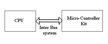
1. Inter System Protocol: The inter system protocol using to communicate the two different devices. Like communication between computer to microcontroller kit. The communication is done through a inter bus system.
Different categories of Inter system protocol:
- UART Protocol
- USART Protocol
- USB Protocol
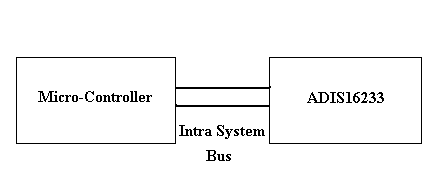
2. Intra System Protocol: The Intra system protocol is used to communicate the two devices within the circuit board. While using this intra system protocols, with out going to intra system protocols we will expand the peripherals of the microcontroller. The circuit complexity and power consumption will be increases by using intra system protocol. Using intra system protocols circuit complexity and power consumption, cost is decrease and it is very secure to accessing the data.
Different categories of Inter system protocol
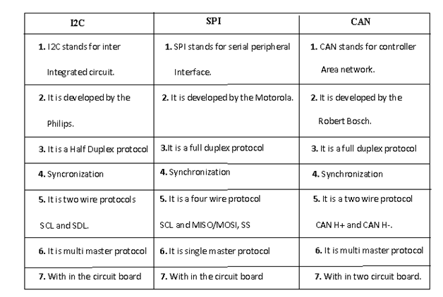
- I2C Protocol
- SPI Protocol
- CAN Protocol
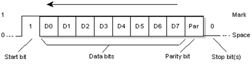
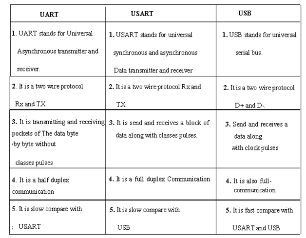
UART Protocol:
UART stands for universal asynchronous transmitter and receiver .UART Protocols is a serial communication with two wired protocol .The data cable signal lines are labeled as Rx and Tx. Serial communication is commonly used for transmitting and receiving the signal. It is transfer and receives the data serially bit by bit without class pulses. The UART take bytes of data and send the individual bits in sequential manner. UART is a half duplex protocol. Half duplex means transferring and receiving the data but not at a same time. Most of the controllers have hardware UART on board. It uses a single data line for transmitting and receiving the data. It has one start bit, 8-bit data and one stop bit mean the 8-bit data transfer ones signal is high to low.
Ex: Emails, SMS, Walkie-talkie.
USART Protocol:
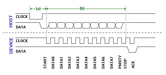
USART stands for universal synchronous and asynchronous transmitter and receiver. It is a serial communication of two wire protocol. The data cable signal lines are labeled as Rx and TX. This protocol is used to transmitting and receiving the data byte by byte along with the clock pulses. It is a full-duplex protocol means transmitting and receiving data simultaneously to different board rates. Different devices communicate with microcontroller to this protocol.
Ex:-Telecommunications.
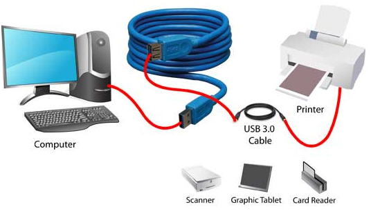
USB Protocol:
USB stands for universal serial bus. Again it is a serial communication of two wire protocol. The data cable signal lines are labeled D+ and D-.This protocol is used to communicate with the system peripherals.USB protocol is used to send and receive the data serially to the host and peripheral devices.USB communication requires a driver software which is based on the functionality of the system.USB device can transfer data on the bus without any request on the host computer. Now a day’s most of the devices are using this technique for communicating with USB protocol. Like computer to communicate with ARM controller using USB. USB transfer the data different modes .first one is slow speed mode 10kbps to 100 kbps; second one is full speed mode 500kbps to 10mbps, high speed mode 25mbps to 400 mbps.USB maximum cable length of 4 meters.
Ex: Mouse, Keyboard, Hubs, switches, pen drive.
Differences Between the Inter System Protocols:
I2C Protocol:
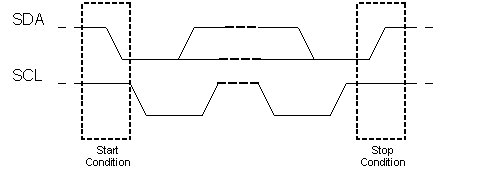
I2C stands for inter integrated circuit. I2C requires only two wires connecting all peripherals to microcontroller.I2C requires two wires SDA (serial data line) and SCL (serial clock line) to carry information between devices. It is a master to slave communication protocol. Each slave has a unique address. Master device sends the address of the target slave device and read/write flag. The address is match any slave device that device is ON, remaining slave devices are disable mode. Once the address is match communication proceed between master and that slave device and transmitting and receiving the data. The transmitter send 8-bit data, the receiver replies 1-bit of acknowledgement. When the communication is completed master issues the stop condition. The I2C bus was developed by Philips Semiconductors. Its original purpose is providing an easy way to connect CPU to peripherals chips. Peripheral devices in embedded systems are often connected to the microcontroller as memory mapped devices. I2C requires only two wires for connecting all the peripherals to the microcontroller. These active wires, called SDA and SCL, are both bidirectional. SDA line is a serial data line and SCA line is a serial clock line.
I2C Pull-up Resistors:
Why given the pull-up resisters in I2C SCL and SDA line.
- Both SDA and SCL lines are open drain drivers.
- Its can be drive output low canot driver it high.
- For the lines to be able to go high you must provide pull-up resistors
SPI Protocol:
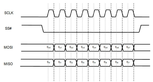
SPI stands for serial peripheral interface. It is one of the serial communication protocol developed by Motorola. Some times SPI protocol is also called a 4-wire protocol. It requires four wires MOSI, MISO, SS, and SCLK.SPI protocol used to communicate the master and slave devices. The master first configures the clock using a frequency. The master then selects the particular slave device for communication by pulling the chip select button. That particular device is selected and starts the communication between master and that particular slave. The master select only one slave at a time. It is full duplex communication protocol. Not limited to 8 bit words in the case of bit transferring.
CAN Protocol:
CAN stands for controller area network .It is a serial communication protocol. It require two wires CAN High (H+) and CAN low (H-). It was developed by the Robert bosh company in 1985 for in vehicle networks. It is based on a message oriented transmission protocol.
Differences Between the Inter System Protocols:
Implementation of Wireless PC Communication System by using Transceiver
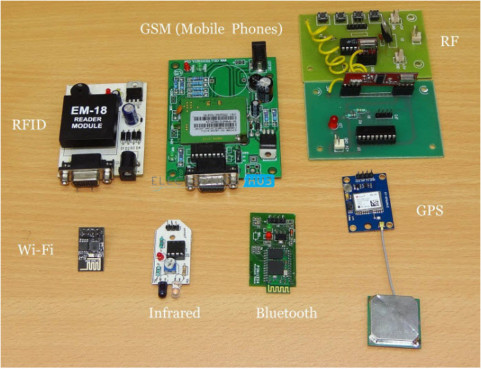
Introduction to Wireless Communication
The transfer of information the points without any physical connections like cables is termed as wireless communication. It is a type of a data communication system. In broad words, wireless communication uses signals for data transmission.
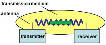
Wireless communication works through electromagnetic signals. These are broadcasted into the atmosphere through a device. The transmitting device can be a sender or an intermediate device which propagates wireless signals. The communication between the two devices occurs when the transmitter and the receiver capture the signal forming a wireless bridge between the devices. Wireless communications are of various types depending on the technology, ecosystem and delivery method. Here are the different communication systems.
- Satellite Communication
- Wireless network communication
- Mobile communication
- Infrared communication
- Bluetooth communication
Though these communication technologies have unique architecture, they work on the transmission and receiving of the data wirelessly.
Wireless communication through Radio Frequency has many advantages as it does not require any line of sight connection between the transmitter and receiver while the line of sight connection exists in infrared communication. A wireless RF transmitter and receiver can be built using HT12D decoder, HT12E encoder, and an RF module. The range of RF communication is high relative to the IR communication. RF transmission is stronger and reliable than the IR transmission because
- The radio frequency signals can travel longer distances than the infrared signals.
- RF signals can be transmitted through the obstacle
- RF signals do not interfere with other RF signals over one frequency band.
Wireless Transmitter
HT12E is an encoder IC Which will convert the 4 bit parallel data given to pins D0 to D3 to serial data and at the output pin Dout. This output serial data are given to the RF transmitter. Address inputs A0 to A7 can be used to provide data security and can be connected to GND (i.e., logic ZERO) or left open (i.e., logic ONE).
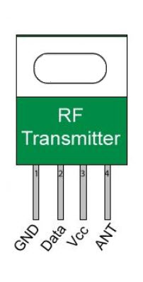
The status of these address pins should match the address pins of the receiver for transmission of data. The data will be transmitted when the Transmit Enable pin (TE) is LOW. The resistor of 750KΩ will provide the external resistance for the operation of the internal oscillator in HT12E.
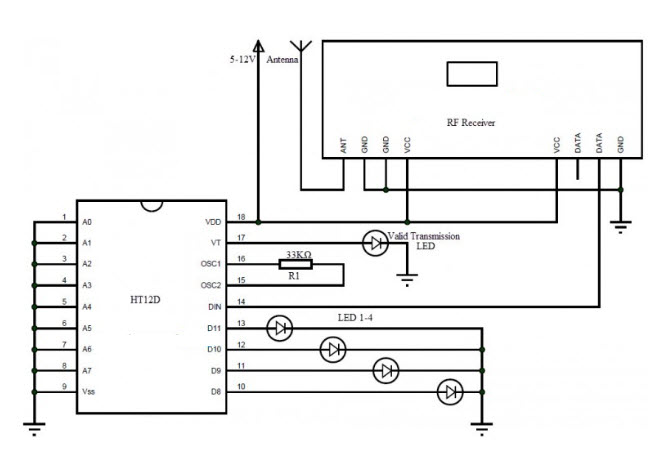
Wireless Receiver
An RF receiver receives the transmitted data from the RF transmitter. HT12D decoder will convert the received serial data to 4 bit parallel data D0 to D3. The status of the address pins A0 to A7 should match with the status of the address pins at HT12E for transmission of the data.
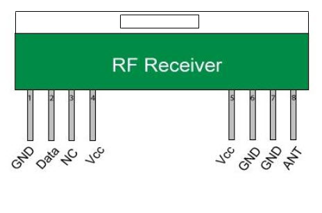
The LEDs connected to the circuit glows when valid data transmits from the transmitter to the receiver. A 33kΩ resistor will provide the necessary for the working of the internal oscillator of HT12D.
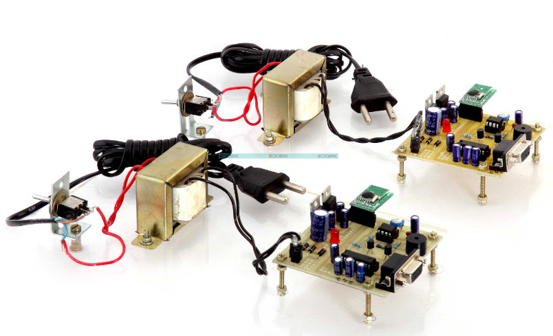
Wireless PC Communication System using Transceiver
The wireless PC communication system uses 2.4GHz trans-receiver to establish communication between the two computers. This system is used in offices for communication between the employees and the manager.
A wireless PC communication system uses a pair of 2.4GHz transceiver module which is powered by 5 volts DC and an alarm circuit. This system is used for bi-directional real-time chat communication from one PC to another using the hyper terminal.
A pair of transceiver modules is connected to the PCs using a DB9 connector and a serial data cord using RS232 protocol is used for communication between the module and the PC. An onboard AC to DC power supply is used at both the ends to power the units.
While one of the users attempts to initiate the chat, an intimation is created using a buzzer sound upon the receipt of the message. Thereafter, the other user can start communication over the chat mode from the PC. Wireless PC communication system project works only on operating systems having hyper terminal and the computer must have an RS232 serial port.
Block Diagram
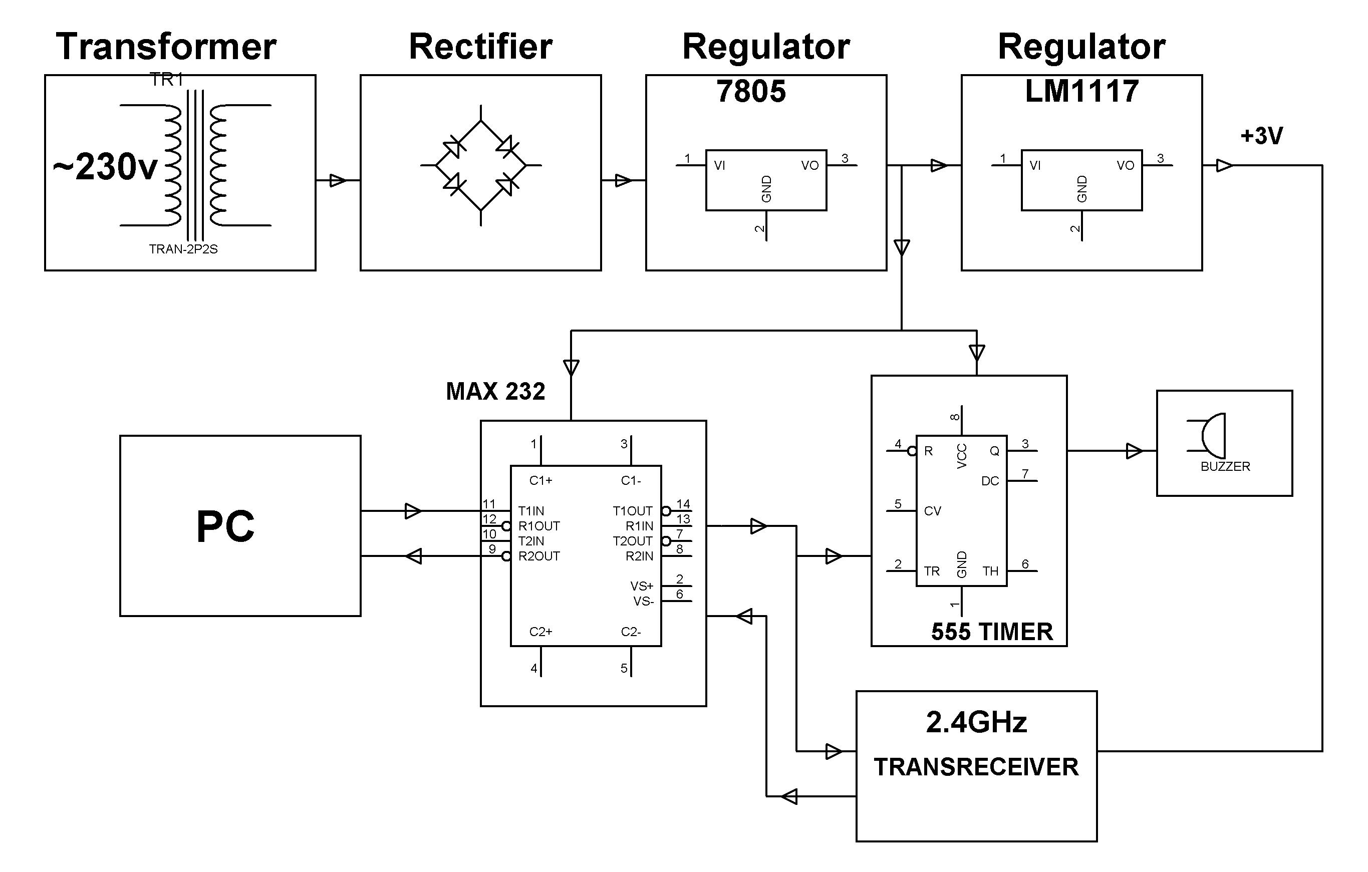
Hardware Requirements
- 2.4GHz Transceiver
- Resistors
- Capacitors
- Diodes
- Transistors
- Transformers
- Voltage Regulator
- 555 Timers
- Buzzer
Circuit Operation
The circuit uses standard power supply comprising of a step-down transformer from 230Vto 12V and 4 diodes forming a bridge rectifier that delivers pulsating DC which is then filtered by an electrolytic capacitor of about 470µF to 1000µF. The filtered DC being unregulated, IC LM7805 and LM1117 are used to get 5V DC constant at its pin no 3 irrespective of input DC varying from 7V to 15V.
555 Timer
A 555 timer is used to provide a time delay in various applications. The timer circuit consists of a 555 timer IC, resistor and capacitor combination and a transistor. The timer circuit is connected to the pin 14 of microcontroller through a slide switch.
A 5V supply is given to pin 8 and 4 of the IC. The 555 timer is used in the astable mode to vary the frequencies. Timer circuit has a male pin connector to interface with the motherboard. Since the frequency cannot be changed, 555 timer circuit is used to generate the artificial frequency
MAX232
The MAX 232 is an integrated circuit used as a voltage converter. This IC is used in communication systems where the voltage level conversion is required to make TTL devices to be compatible with RS 232 standards of PC serial ports and vice versa.
The controller operates at TTL logic level (0-5v) while the serial communication PC works at RS232 standards (+25v to -25v). This makes it difficult to establish a direct link for communication. MAX 232 acts as an intermediate link between them. MAX 232 is a dual transmitter/receiver that is typically used to convert the RX, TX, CTS and RTS signals.
2.4GHz Transceiver
This is an RF-based 2.4GHz frequency transceiver designed for low power wireless applications. The RF transceiver is integrated with a highly configurable baseband modem. This is a low-cost device.
This concept is future can be further enhanced to link a number of systems forming a network of computers so that a number of employees can communicate with each other.
Applications of wireless communication
- Wireless security systems
- Car alarm systems
- Sensor reporting
- Remote control
- Automation system
Thus, this is all about Wireless PC communication system and its applications. We hope that you have got a better understanding of this concept.
4. let us discuss the science of electronics to provide Commitment
Remote Controlled Robotic Arm
o reduces the human efforts and in industries to increase efficiency, proficiency and the most important is to reduce the time. Nowadays a new technology of Robotics is used which can do a specific task. These Robots are controlled with the remote. The Robot is programmed for the specific task. Every task of the robot is defined; stoppage timing of the robot and angle of rotation between the two places is defined by the servo motors. This is very wonderful project to control the working of the robotic arm without wire.
It is to control a robotic arm using the remote control. The remote control works on the RC5 PROTOCOL. It transmits 14 data at a time. The command data is a Manchester coded bit stream modulating a 36 kHz carrier. The IR signal from the transmitter is detected by a specialized IC (IR receiver) with an integral photo-diode, and is amplified, filtered, and demodulated. The 14 bit contains 2 start bit, 1 toggle bit, 5 address bit and 6 command bit. By receiving the data the coding is done for the operation of the servo motors. As for the particular bit pattern the particular number or motors are to be operated for a particular angle. In this way the robotic arm is controlled using the remote control.
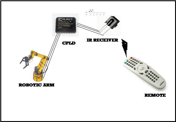
Importance of the Research
To reduces the human efforts, and in industries to increase efficiency, proficiency and the most important is to reduce the time. Through this a person who has no hand can also work by using the robotic arm as a temporary hand.
Contribution
It concludes the VLSI implementation of the Remote Controlled Robotic Arm. In this hardware is designed for servo motor by which the motion of the robotic arm can be controlled. Although these do not fall under the category of mobile robotics, the field of robotics essentially started with arms and end-effectors (devices that attach to the end of an arm such as grippers, electromagnets etc). Arms and grippers are the best way for a robot to interact with the environment it is exploring. Simple robot arms can have just one motion, while more complex arms can have a dozen or more unique degrees of freedom
Servo motors are types of actuators that rotate to a specific angular position, and were classically used in more expensive remote controlled vehicles for steering or controlling flight surfaces. Now that they are used in a variety of applications, the price of hobby servos has gone down significantly, and the variety (different sizes, technologies, and strength) has increased A hobby servo motor actually includes a DC motor, gearing, electronics and a rotary potentiometer (which, in essence, measures the angle). The electronics and potentiometer work in unison to activate the motor and stop the output shaft at a specified angle. These servos are generally have three wires: ground, voltage in, and a control pulse. The control pulse is usually generated with a servo motor controller. A "robot servo" is a new type of servo that offers both continuous rotation and position feedback. All servos can rotate CW and CCW .
Railway Switches And Signals
Signals, including those used for communication between occupants of a car or train.Indicators, recorders, telegraphic, telephonic, or other similar apparatus when especially designed for use in connection with car or train movements, except manually-set devices, such as train and engine signs and markers capable of general use.
Devices on the roadway, such as signals, switches, circuit closures, gates, etc., actuated or controlled from or by the moving vehicles, except circuit-controllers actuated by the vehicle for the purpose of energizing sectionalized conductors used for supplying propulsion-current thereto.
Automatic train stop and speed control means, the actuation of which is initiated by agencies not on the train or by wheel derailment or defects in train structure and mechanism, the automatic stop, for classification purposes, being considered an equivalent of and substitute for a railway signal; but train stopping and control mechanism cooperating with obstacles fixed in position upon the track which have no moving parts are excluded from this class except when they cooperate with speed-responsive devices on the train.
Safety devices, including derailing switches and blocks, used for preventing accidents caused by the misplacement of switches, disregard of signals etc.The structure of signals, switches, frogs, and crossings and their appurtenances.Mechanism for the manual or other actuation of any of the devices of the class.
Electronic Number Lock
A lock is an integral part of every house. A man can have peace of mind only when he has a proper mechanism to lock his house when he is away. At present mechanical locks are being used. These locks have levers in them that are used to lock or unlock the unit. Keys that have a particular pattern of cuts and notches on them control these levers. Each lock opens only if the pattern of cuts and notches inside it match with the pattern on the key.
The main disadvantage of this mechanism is that one cannot open the lock if one has lost or misplaced the key. The house owner will be stranded outside his house if he loses the keys to his front door. This conventional lock-and-key mechanism poses a lot of security problems too. Any number of duplicate keys can be easily made from the original key. These duplicate keys may be used for unauthorized access without the knowledge of the owner. Burglars may find the right key to open the lock by trying different keys one after the other from a bunch of keys. An expert thief doesn't even need a proper key to open a lock. He can merely do it with a hairpin. If everything else fails, the thief can physically break open the lock.
An Electronic Number Lock system opens only when the user types in the correct code set earlier. Unauthorized access is impossible since no one can enter without the knowledge of the code. The entry of a wrong code more than twice sets off a buzzer that informs the owner or neighbours of an intruder. Since the locking mechanism is placed inside the house, tampering with the lock is not possible. Multiple access is possible since anyone possessing the code can open the lock. This is not possible with the conventional lock-and-key mechanism unless each user has his own key. The code number to open the lock can be easily changed by the user whenever he wishes. This lock can be used in homes, cars, safes or anywhere where there is a locking requirement. Thus, this innovative project provides a safe and tamper-proof locking solution.
+++++++++++++++++++++++++++++++++++++++++++++++++++++++++++++++++
C 4
I am the owner of the 911electronic.com website.
BalasHapusWe have an article on the subject of a simple-dial diode on your website. We describe in it the principle of operation, structure, and characteristics for the use of a rectifying diode. The article describes various types of rectifier bridges.
The article under the link http://jessicasiboro.blogspot.com/2018/07/electronics-is-field-of-science-that-is.html contains a very extensive knowledge of electronics. This is one of the best articles I've read and one of the longest.
It describes the Wireless PC Communication System using Transceiver. To create this project we need a bridge rectifier, the subject of which is not discussed in the article.
Our site has an article on diode rectification and on the subject of rectifier bridges. We describe in it, for example: Half wave rectifier bridge, Bridge rectifier and full wave rectifier, Three phase rectifier bridge.
Please read our article and state whether it would extend the information to your readers. If so, I would like to create a link in the text to our article.