
Drawing electronic circuits or designing electronic images is very important for an electronic engineering instructor or an expert in electronics engineering especially for the development of electronic products products both in the field of services and manufacturing because the product of the product of production in the industry at the present time is the result of the setting of the tool control device electronics let's call it e-Clarity. electronics engineering at the moment is much related to the working system and processing of materials that used to be and new materials that we surely find when we detect it using electronics detection equipment to new materials both on earth and outside the earth orbit. when drawing the design of electronics in the early stages must be we printing and drawing graffiti in a paper or computer desk and required the power of peace of mind in the right circumstances because an electronic picture and design very important in the application on earth at the moment. at the time of the 20th century and the 21st century today a picture of electronics and electronics design is still adapted to component components available on the market or component components that we met, for the next stage in the development of electronics industry to support and support the development of the pharmaceutical industry and industry Avionics because at this time both industries are still confined to manual machine pattern not in electronics Design control and application consistent and stable: (e - C4 = e - Clarity <-> e - Consistency <-> e - communication <-> e - commitment). let's review the drawing technique of electronics circuits at the moment:
1. The technique of drawing electronics circuit based on the form of the signal in
sequence in sequence.
2. The technique of drawing electronics circuit based on block diagram (diagram
the workflow of the signal from input to output or we call it from the input transducer to
the process component then to the transducer ouput then in the feedback
through component settings or count rolling components.
3. The technique of drawing electronics circuits based on symbols and symbols
the symbol of an electronic component component in which the symbol emblem
components of electronic circuits that exist at this time the number could be dozens
thousand types of electronic components that exist today outside of the components
only made for the benefit of a trip into space.
4. The technique of drawing electronics circuit based on the photo of the component
actually from the electronics component is so for a technician
electronics more visible in bentu 2 dimension (2D) to 3 dimension (3D)
5. The technique of drawing electronics circuit using flow chart or
flow chart example: start setting start then setting form then component
processes such as diodes, transistors, ICs (integrated circuit). Microprossesor,
Microcontroller, nano processor, nano controller. then to the state of action
which is in the position of YES and JESS.
6. The technique of drawing electronics circuit using manual hand book
ie only the use of the tool from the menu menu and installation of tools
electronics.
so a little of the design and depiction of electronics in the 20th and 21st centuries today. when we enter the next generation we must be better, more true, more efficient, more and more SMART and DILIGENT. this is what I will describe and explain as below.
GEN. Mac Tech


How to Read a Schematic
Overview
Schematics are our map to designing, building, and troubleshooting circuits. Understanding how to read and follow schematics is an important skill for any electronics engineer.
This tutorial should turn you into a fully literate schematic reader! We’ll go over all of the fundamental schematic symbols:
Then we’ll talk about how those symbols are connected on schematics to create a model of a circuit. We’ll also go over a few tips and tricks to watch out for.
Suggested Reading
Schematic comprehension is a pretty basic electronics skill, but there are a few things you should know before you read this tutorial. Check out these tutorials, if they sound like gaps in your growing brain:
Schematic Symbols (Part 1)
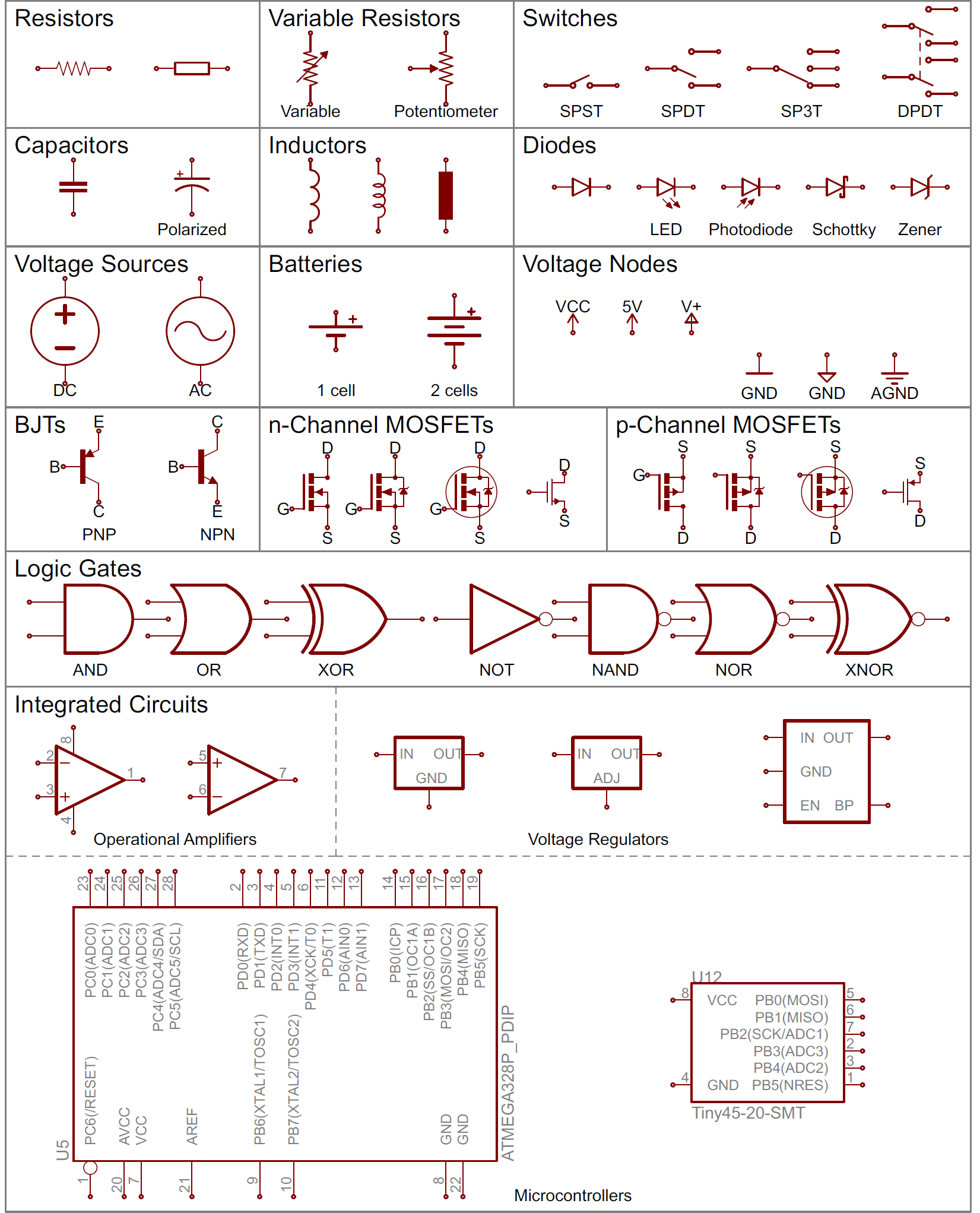
Are you ready for a barrage of circuit components? Here are some of the standardized, basic schematic symbols for various components.
Resistors
The most fundamental of circuit components and symbols! Resistors on a schematic are usually represented by a few zig-zag lines, with two terminals extending outward. Schematics using international symbols may instead use a featureless rectangle, instead of the squiggles.
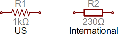
Potentiometers and Variable Resistors
Variable resistors and potentiometers each augment the standard resistor symbol with an arrow. The variable resistor remains a two-terminal device, so the arrow is just laid diagonally across the middle. A potentiometer is a three-terminal device, so the arrow becomes the third terminal (the wiper).
Capacitors
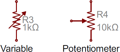
There are two commonly used capacitor symbols. One symbol represents a polarized (usually electrolytic or tantalum) capacitor, and the other is for non-polarized caps. In each case there are two terminals, running perpendicularly into plates.
The symbol with one curved plate indicates that the capacitor is polarized. The curved plate represents the cathode of the capacitor, which should be at a lower voltage than the positive, anode pin. A plus sign might also be added to the positive pin of the polarized capacitor symbol.
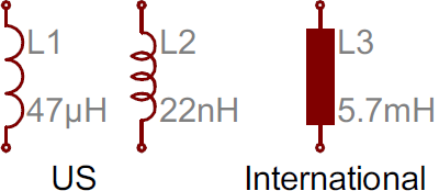
Inductors
Inductors are usually represented by either a series of curved bumps, or loopy coils. International symbols may just define an inductor as a filled-in rectangle.
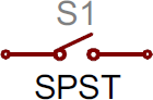
Switches
Switches exist in many different forms. The most basic switch, a single-pole/single-throw (SPST), is two terminals with a half-connected line representing the actuator (the part that connects the terminals together).
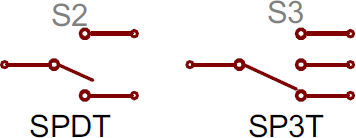
Switches with more than one throw, like the SPDT and SP3T below, add more landing spots for the the actuator.
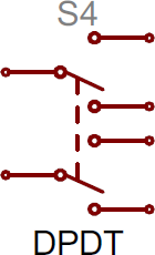
Switches with multiple poles, usually have multiple, alike switches with a dotted line intersecting the middle actuator.
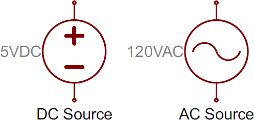
Power Sources
Just as there are many options out there for powering your project, there are a wide variety of power source circuit symbols to help specify the power source.
DC or AC Voltage Sources
Most of the time when working with electronics, you’ll be using constant voltage sources. We can use either of these two symbols to define whether the source is supplying direct current (DC) or alternating current (AC):
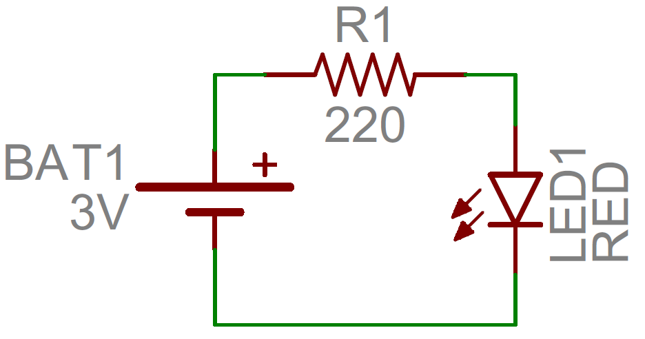
Batteries
Batteries, whether they’re those cylindrical, alkaline AA’s or rechargeable lithium-polymers, usually look like a pair of disproportionate, parallel lines:
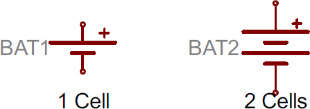
More pairs of lines usually indicates more series cells in the battery. Also, the longer line is usually used to represent the positive terminal, while the shorter line connects to the negative terminal.
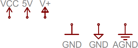
Voltage Nodes
Sometimes – on really busy schematics especially – you can assign special symbols to node voltages. You can connect devices to these one-terminal symbols, and it’ll be tied directly to 5V, 3.3V, VCC, or GND (ground). Positive voltage nodes are usually indicated by an arrow pointing up, while ground nodes usually involve one to three flat lines (or sometimes a down-pointing arrow or triangle).
Schematic Symbols (Part 2)
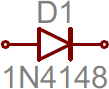
Diodes
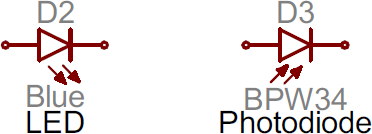
Basic diodes are usually represented with a triangle pressed up against a line. Diodes are also polarized, so each of the two terminals require distinguishing identifiers. The positive, anode is the terminal running into the flat edge of the triangle. The negative, cathode extends out of the line in the symbol (think of it as a - sign).
There are a all sorts of different types of diodes, each of which has a special riff on the standard diode symbol. Light-emitting diodes (LEDs) augment the diode symbol with a couple lines pointing away. Photodiodes, which generate energy from light (basically, tiny solar cells), flip the arrows around and point them toward the diode.
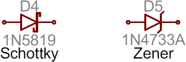
Other special types of diodes, like Schottky’s or zeners, have their own symbols, with slight variations on the bar part of the symbol.
Transistors
Transistors, whether they’re BJTs or MOSFETs, can exist in two configurations: positively doped, or negatively doped. So for each of these types of transistor, there are at least two ways to draw it.
Bipolar Junction Transistors (BJTs)
BJTs are three-terminal devices; they have a collector (C), emitter (E), and a base (B). There are two types of BJTs – NPNs and PNPs – and each has its own unique symbol.
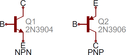
The collector (C) and emitter (E) pins are both in-line with each other, but the emitter should always have an arrow on it. If the arrow is pointing inward, it’s a PNP, and, if the arrow is pointing outward, it’s an NPN. A mnemonic for remembering which is which is “NPN: not pointing in.”
Metal Oxide Field-Effect Transistors (MOSFETs)
Like BJTs, MOSFETs have three terminals, but this time they’re named source (S), drain (D), and gate (G). And again, there are two different versions of the symbol, depending on whether you’ve got an n-channel or p-channel MOSFET. There are a number of commonly used symbols for each of the MOSFET types:
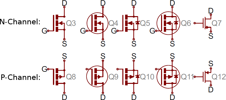
The arrow in the middle of the symbol (called the bulk) defines whether the MOSFET is n-channel or p-channel. If the arrow is pointing in means it’s a n-channel MOSFET, and if it’s pointing out it’s a p-channel. Remember: “n is in” (kind of the opposite of the NPN mnemonic).
Digital Logic Gates
Our standard logic functions – AND, OR, NOT, and XOR – all have unique schematic symbols:

Adding a bubble to the output negates the function, creating NANDs, NORs, and XNORs:

They may have more than two inputs, but the shapes should remain the same (well, maybe a bit bigger), and there should still only be one output.
Integrated Circuits
Integrated circuits accomplish such unique tasks, and are so numerous, that they don’t really get a unique circuit symbol. Usually, an integrated circuit is represented by a rectangle, with pins extending out of the sides. Each pin should be labeled with both a number, and a function.
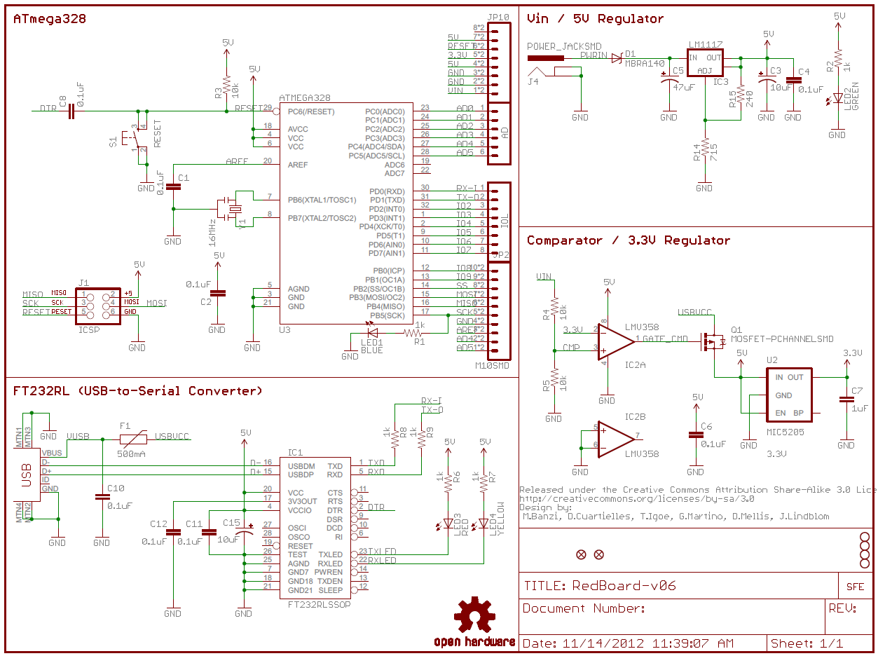
Schematic symbols for an ATmega328 microcontroller (commonly found on Arduinos), an ATSHA204 encryption IC, and an ATtiny45 MCU. As you can see, these components greatly vary in size and pin-counts.
Because ICs have such a generic circuit symbol, the names, values and labels become very important. Each IC should have a value precisely identifying the name of the chip.
Unique ICs: Op Amps, Voltage Regulators
Some of the more common integrated circuits do get a unique circuit symbol. You’ll usually see operation amplifiers laid out like below, with 5 total terminals: a non-inverting input (+), inverting input (-), output, and two power inputs.
Often, there will be two op amps built into one IC package requiring only one pin for power and one for ground, which is why the one on the right only has three pins.
Simple voltage regulators are usually three-terminal components with input, output and ground (or adjust) pins. These usually take the shape of a rectangle with pins on the left (input), right (output) and bottom (ground/adjust).
Miscellany
Crystals and Resonators
Crystals or resonators are usually a critical part of microcontroller circuits. They help provide a clock signal. Crystal symbols usually have two terminals, while resonators, which add two capacitors to the crystal, usually have three terminals.
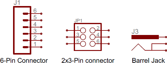
Headers and Connectors
Whether it’s for providing power, or sending out information, connectors are a requirement on most circuits. These symbols vary depending on what the connector looks like, here’s a sampling:
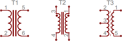
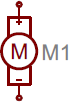
Motors, Transformers, Speakers, and Relays
We’ll lump these together, since they (mostly) all make use of coils in some way. Transformers (not the more-than-meets-the-eye kind) usually involve two coils, butted up against each other, with a couple lines separating them:
Relays usually pair a coil with a switch:

Speakers and buzzers usually take a form similar to their real-life counterparts:

And motors generally involve an encircled “M”, sometimes with a bit more embellishment around the terminals:
Fuses and PTCs
Fuses and PTCs – devices which are generally used to limit large inrushes of current – each have their own unique symbol:
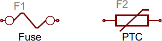
The PTC symbol is actually the generic symbol for a thermistor, a temperature-dependent resistor (notice the international resistor symbol in there?).
No doubt, there are many circuit symbols left off this list, but those above should have you 90% literate in schematic reading. In general, symbols should share a fair amount in common with the real-life components they model. In addition to the symbol, each component on a schematic should have a unique name and value, which further helps to identify it.
Name Designators and Values
One of the biggest keys to being schematic-literate is being able to recognize which components are which. The component symbols tell half the story, but each symbol should be paired with both a name and value to complete it.
Names and Values
Values help define exactly what a component is. For schematic components like resistors, capacitors, and inductors the value tells us how many ohms, farads, or henries they have. For other components, like integrated circuits, the value may just be the name of the chip. Crystals might list their oscillating frequency as their value. Basically, the value of a schematic component calls out its most important characteristic.
Component names are usually a combination of one or two letters and a number. The letter part of the name identifies the type of component – R’s for resistors, C’s for capacitors, U’s for integrated circuits, etc. Each component name on a schematic should be unique; if you have multiple resistors in a circuit, for example, they should be named R1, R2, R3, etc. Component names help us reference specific points in schematics.
The prefixes of names are pretty well standardized. For some components, like resistors, the prefix is just the first letter of the component. Other name prefixes are not so literal; inductors, for example, are L’s (because current has already taken I [but it starts with a C…electronics is a silly place]). Here’s a quick table of common components and their name prefixes:
| Name Identifier | Component |
|---|---|
| R | Resistors |
| C | Capacitors |
| L | Inductors |
| S | Switches |
| D | Diodes |
| Q | Transistors |
| U | Integrated Circuits |
| Y | Crystals and Oscillators |
Although theses are the “standardized” names for component symbols, they’re not universally followed. You might see integrated circuits prefixed with IC instead of U, for example, or crystals labeled as XTAL’s instead of Y’s. Use your best judgment in diagnosing which part is which. The symbol should usually convey enough information.
Reading Schematics
Understanding which components are which on a schematic is more than half the battle towards comprehending it. Now all that remains is identifying how all of the symbols are connected together.
Nets, Nodes and Labels
Schematic nets tell you how components are wired together in a circuit. Nets are represented as lines between component terminals. Sometimes (but not always) they’re a unique color, like the green lines in this schematic:
Junctions and Nodes
Wires can connect two terminals together, or they can connect dozens. When a wire splits into two directions, it creates a junction. We represent junctions on schematics with nodes, little dots placed at the intersection of the wires.
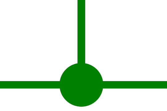
Nodes give us a way to say that “wires crossing this junction are connected”. The absences of a node at a junction means two separate wires are just passing by, not forming any sort of connection. (When designing schematics, it’s usually good practice to avoid these non-connected overlaps wherever possible, but sometimes it’s unavoidable).
Net Names
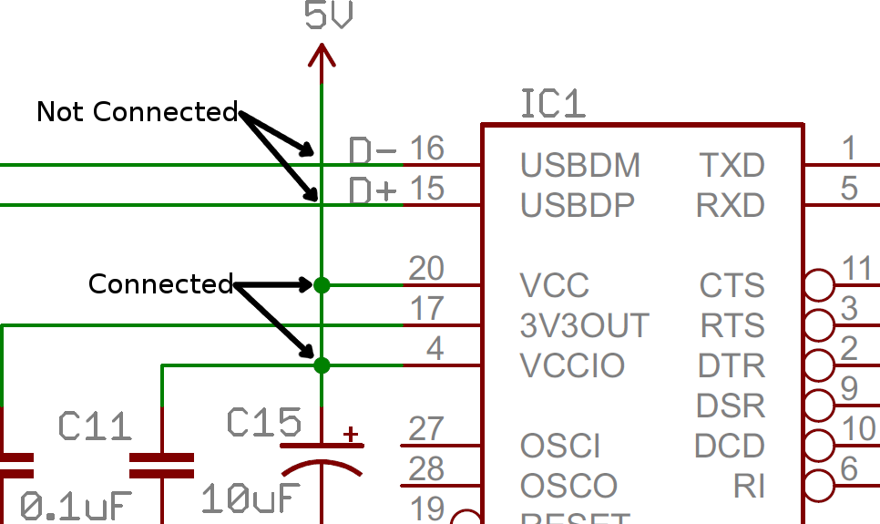
Sometimes, to make schematics more legible, we’ll give a net a name and label it, rather than routing a wire all over the schematic. Nets with the same name are assumed to be connected, even though there isn’t a visible wire connecting them. Names can either be written directly on top of the net, or they can be “tags”, hanging off the wire.
Each net with the same name is connected, as in this schematic for an FT231X Breakout Board. Names and labels help keep schematics from getting too chaotic (imagine if all those nets were actually connected with wires).
Nets are usually given a name that specifically states the purpose of signals on that wire. For example, power nets might be labeled “VCC” or “5V”, while serial communication nets might be labeled “RX” or “TX”.
Schematic Reading Tips
Identify Blocks
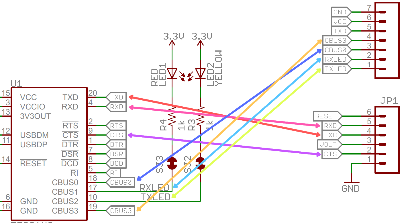
Truly expansive schematics should be split into functional blocks. There might be a section for power input and voltage regulation, or a micro controller section, or a section devoted to connectors. Try recognizing which sections are which, and following the flow of circuit from input to output. Really good schematic designers might even lay the circuit out like a book, inputs on the left side, outputs on the right.
If the drawer of a schematic is really nice they may separate sections of a schematic into logical, labeled blocks.
Recognize Voltage Nodes
Voltage nodes are single-terminal schematic components, which we can connect component terminals to in order to assign them to a specific voltage level. These are a special application of net names, meaning all terminals connected to a like-named voltage node are connected together.
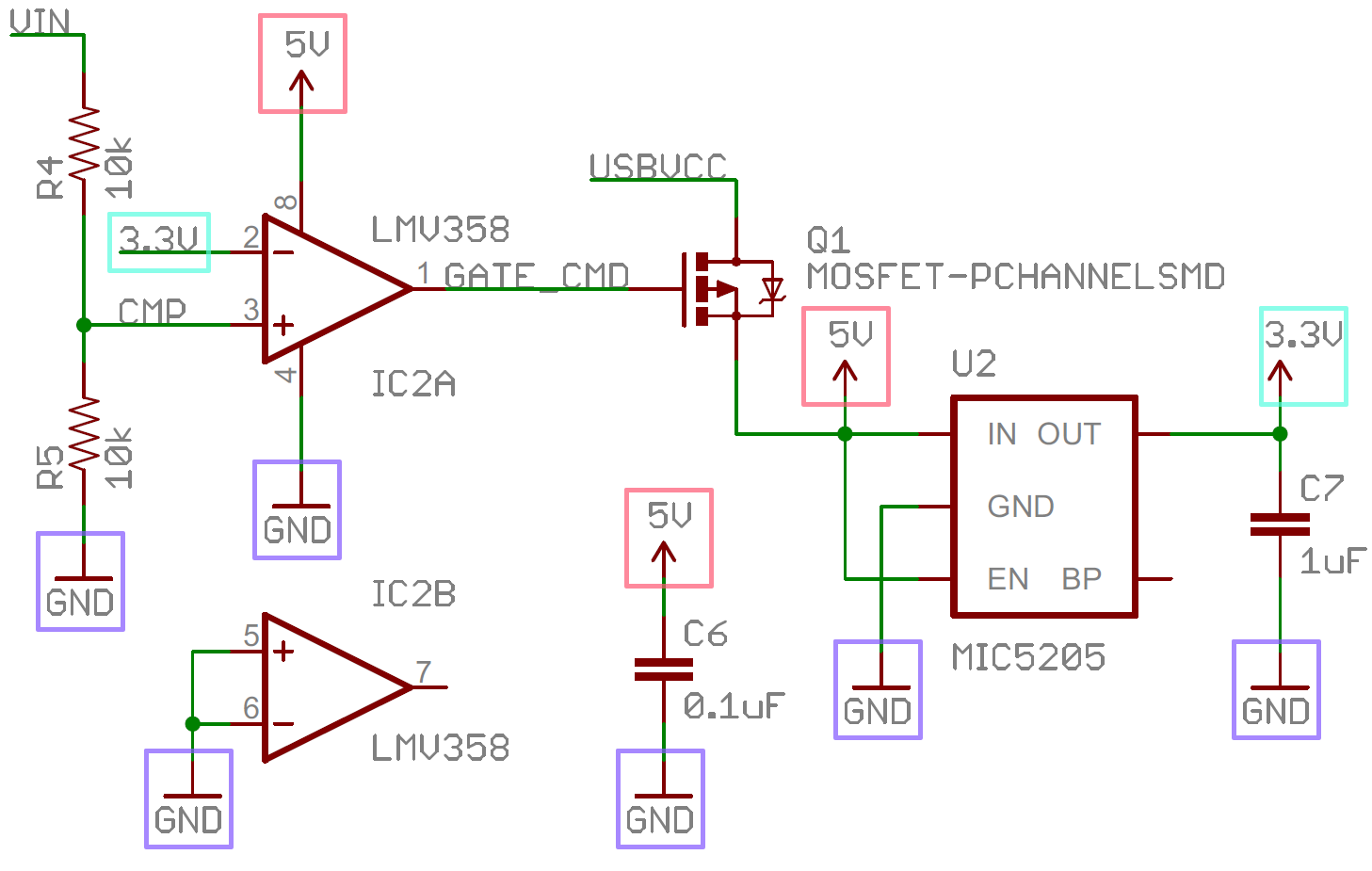
Like-named voltage nodes – like GND, 5V, and 3.3V – are all connected to their counterparts, even if there aren’t wires between them.
The ground voltage node is especially useful, because so many components need a connection to ground.
Reference Component Datasheets
If there’s something on a schematic that just doesn’t make sense, try finding a datasheet for the most important component. Usually the component doing the most work on a circuit is an integrated circuit, like a microcontroller or sensor. These are usually the largest component, oft-located at the center of the schematic.
Resources
Knowing component symbols, following nets, and identifying common labels. Understanding how a schematic works opens up the whole world of electronics to you ! :
- Voltage Dividers - This is one of the most basic, fundamental circuits.
- How to Use a Breadboard - Now that you know how to read schematics, why not make one! Breadboards are a great way to make temporary, functional, prototype circuits.
- Working with Wire - Or, skip the breadboard and jump straight into wiring stuff up. Knowing how to cut, strip, and connect wire is an important electronics skill.
- Series and Parallel Circuits - Building circuits in series or parallel requires a good understanding of schematics.
- Sewing with Conductive Thread - If you don’t want to work with wire, how about building an e-textiles circuit with conductive thread? That’s the beauty of schematics, the same schematic circuit can be built in a number of different ways with a number of different mediums.
XO__XO Circuit Diagram Drawing Software
When it comes to drawing circuit diagrams, it’s damn hard to get a clear overview of all the benefits and functionalities different tools have to offer. However, in the end, everybody needs one, so it’s important to know which circuit diagram maker is best tailored to your personal needs.
In the virtual world, an electronic component is represented by a symbol. These symbols are used in the 2D and 3D representation of diagram circuits. All these symbols are linked with straight lines that represent the electrical wires. Taking a step further, all these symbols and lines form a diagram that is used to show you how to connect in an optimal way the electronic components. The final step is using the simulation tool to determine the design defects and deficiencies.
In the following, we explore a series of online and computer software tools for drawing circuit diagrams.
Online tools to draw circuit diagrams
In general, the tools used to draw circuit diagrams in a browser are simple and allows you to produce schematic diagrams at a click away. Any of these online tools can be comparatively with computer software designed for the same purpose. The reason is simple. All the features of a computer software can be implemented in a browser tool for circuit diagrams.
In this category, I made a list with several free online tools that run in a browser and useful for drawing circuit diagrams.

SchemeIt
- SchemeIt
With a comprehensive list of electronic symbols and components, SchemeIt is one of the most completed, simple and useful online schematic and diagramming tool. The tool offers support for drawing and export the electronic circuit as an image, or just to share the work with other users. A complete electronic symbol library makes the work easier for everyone. SchemeIt is compatible with almost all web browsers and is free for use. - CircuitLab
Besides building circuits, the CircuitLab has integrated a simulator designed to be used by anyone to test the electronic schema just using the browser. It has a user-friendly interface and offers an accurate analysis of DC or AC electronic components. The CircuitLab tool uses the drag-and-drop gesture while the electronic elements are linked with fewer clicks.
It can be used for educational purposes or by hobbyists to learn the electronic concepts, or used by practicing engineers to explore the design in the same way as traditional tools. - Draw
Draw is a simple and useful online diagramming application with cloud storage integration to store your files online and access easily the circuit diagrams from anywhere and anytime. The tool is fast, simple and reliable. The Draw was built using mxGraph JavaScript library, and the result is a web application with export options, a lot of symbols and the possibility to embed widget sharing. - Webtronics
Webtronics is a simple and free online tool for designing schematic circuit diagrams. It allows you to export the electronic schema as a simple image, and to import and edit schematic images. - Falstad
Falstad is an electronic circuit simulator that runs in browser as a Java applet. Its design is based on colors that can indicate for example positive or negative voltage, and allows you to build simple circuits with mouse clicks. - EasyEDA
EasyEDA is a great free web based PCB tool for anyone involved in electronics design and able to share the work with others. The tool allows you to import an old design from several other circuit maker tools, it has the ability to export the designs and simulation results in .PNG or .SVG formats, and can be a host for your partners and colleagues if they want to work on your projects.
Computer software to draw circuit diagrams
A computer software offers different ways to manipulate and organize the electrical circuits including here the possibility to import files, share, and work with complex electronic scheme.
In the following you have available a series of computer software tools to draw and simulate electronic circuits and diagrams.

SmartDraw
- SmartDraw
SmartDraw is a free software designed to create diagrams for electronic circuits. It has a simple and friendly interface based on drag-and-drop gestures. The tool uses simple commands for shapes while the program automatically adjusts the position with the appropriate connections. - TinyCAD
Based on standard and custom symbol libraries, TinyCAD is an open source tool for drawing circuit diagrams. - Dia
Dia is a program to draw structured diagrams. - PSPICE 9.1
PSPICE is also available in student version and is used to draw and simulate analog and digital circuits. - KiCad
KiCad is a free EDA software for professional schematics and printed circuit boards. - FreePCB
FreePCB is an open-source and free diagram tool designed for Windows OS with support for import and export files. - Circuit Diagram
Circuit Diagram is an open-source and free software used to design electronic circuit diagrams. The tool has support to export the digital circuit in images. - gEDA
gEDA is a free drawing tool for a large variety of electronic fields including electrical circuit design, schematic capture, simulation, prototyping, and production. - Solve Elec
Solve Elec is a free tool used to draw and analyze electrical circuits for alternative and direct current. The software offers the possibility to integrate documentation in the project. - EAGLE PCB
EAGLE PCB is a software with the aim to offer a complete design tool to experts in electronics. It has incorporated not just one module, it has incorporated three modules embedded in one interface. - EDWinXP
EDWinXP is not just a drawing tool, this is a complete software package used to design electronic products. From an idea to the final product are many stages, and all of these stages are covered by this tool. The EDWinXP has support for 3D designs. - Linear Technology
Linear provides a wide range of tools used for modeling and simulate electronic circuits. - NI Multisim
NI Multisim is a complete tool to draw circuits, and it’s used especially for educational purposes. - PCB123
PCB123 software offers a complete range of tools for design and print circuits. - PowerVue Circuit Analyzer
PowerVue tool is dedicated to electrical engineers and used in small and medium projects. Its features include calculating voltage drops and branch currents and also display voltage and current vectors. - DipTrace
DipTrace is a complete tool and has a friendly interface for drawing schemes. The library is a huge box with over 100,000 parts used to design 3D models. The tool offers support for a large number of output formats in order to fit with various manufacturers. - 5Spice
5Spice offers the ability to integrate the drawing circuits with simulation results, and offer support for an unlimited number of analyzes. - TINA
Tina is a powerful design suite tool with circuit simulation and for PCB design. - AmpereSoft ProPlan
AmpereSoft ProPlan is a complete tool to draw circuit diagrams, assembly plans, terminal tables and part lists. - Stylus Labs
Compatible with Windows, Linux, Mac or Android operating systems, Stylus Labs is a simple software with support for the SVG file format that allows you to view the documents in any browser. - Inkscape
Inkscape has sophisticated drawing tools for diagrams and is one of the designing tools for professional users. It is free and open-source software, which runs on Windows, Mac OS X, and Linux. - AVSnap
AVSnap is a free software to draw a detailed circuit diagram. - OmniGraffle
OmniGraffle is a multipurpose drawing tool with powerful styling tools that can organize diagrams with just one click. - Fritzing
With a large community of users, the Fritzing is a useful design tool for Arduino projects. You can share your work with all users, or you can be helped by people in the community. - LTspice IV
Compatible with Windows and Mac OS X, the LTspice IV is a high-performance SPICE simulator and schematic capture. - Circuit Diagram
A simple Windows design tool for making electronic circuit diagrams.
Example of How to Draw Electrical and Electronic Diagrams with Smart Draw ?
Making wiring or electrical diagrams is easy with the proper templates and symbols:
- Start with a collection of electrical symbols appropriate for your diagram
- Draw circuits represented by lines
- Drag and drop symbols to the circuits and connect them
- Use line hops if any lines need to cross
- Add layers to show complexity
Smart Draw has several tools and templates for making a variety of visuals for engineering and CAD design. Among these you'll find commonly used electrical drawings and schematics, like circuit diagrams, wiring diagrams, electrical plans and block diagrams. With Smart Draw's vast library of electrical symbols and easy drawing tools, anyone - apprentice or pro - can start building electrical diagrams right away.
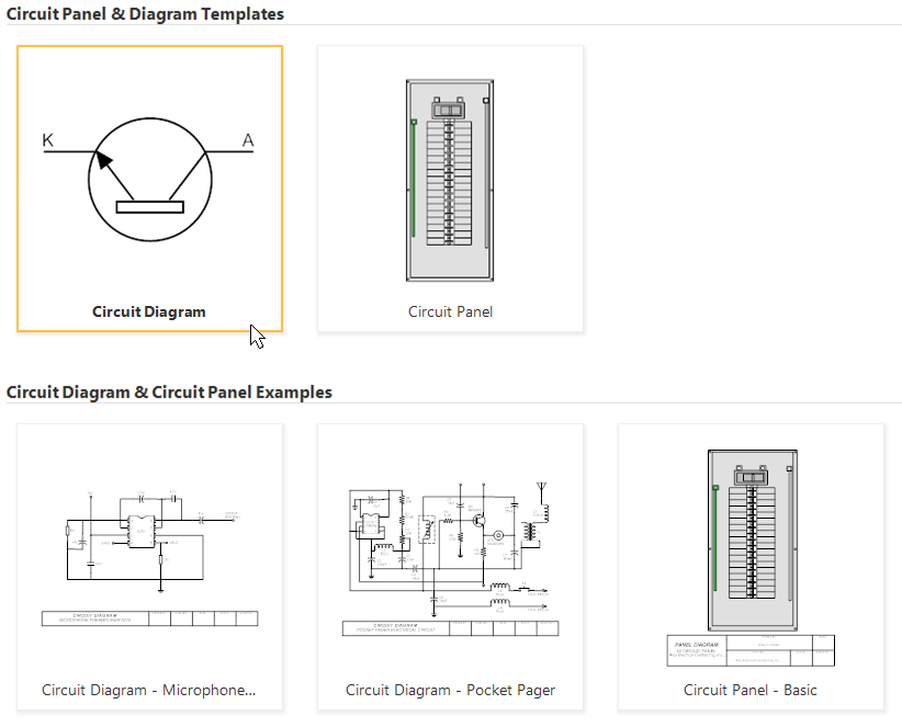
Start with a Circuit Diagram Template
Let's start by making a circuit diagram. To find a circuit diagram template, click on the Engineering & CAD category then Circuit Panels in SmartDraw's Template Browser. Open the template called "Basic Electrical". While you'll start with a blank page, you'll notice a wide range of electrical symbols docked in the SmartPanel to the left of your drawing area. These capacitors, inductors, switches, resisters, and more will make building your circuit diagram easier.
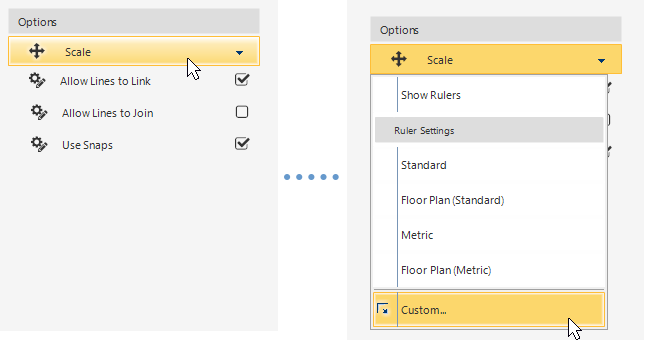
Set Some Defaults
You circuit diagram will basically visualize circuits as lines and the added symbols will indicate where switches and fusers may go. Depending on how you prefer to work, you may want to set some defaults for your entire diagram. These settings are conveniently located at the bottom of your SmartPanel. The scale is set by default as 1/8, as in one inch on the screen will represent 8 feet. You can customize the scale or change it to metric before you start.
The line settings will help you draw your circuits. If the Allow Lines to Link option is selected in the SmartPanel, the lines will neatly snap to each other. If the Allow Lines to Join option is selected, these connected lines will stay together once connected. Having Use Snaps selected will help lines and symbols snap to the nearest grid point as you draw.
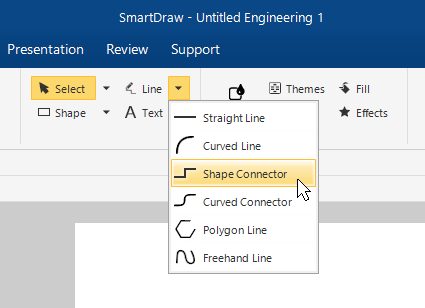
Draw Circuit Lines
Start drawing lines by clicking on the Draw Lines tool in the SmartPanel. By default, you'll draw a straight line. If you want to change the type of line you're drawing, select a line type from the Line Shape drop down. If you right click on a line, you can change its line shape even after you've added it to the page,as well as add arrowheads if you need.
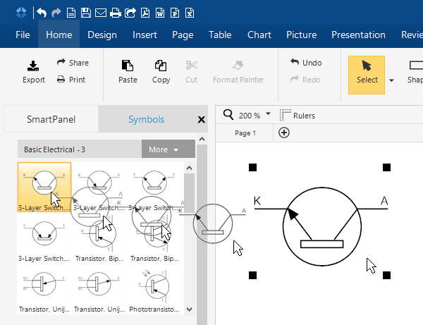
Add Symbols
Drag a symbol from the docked library onto the line and it will automatically insert itself. You can move it along the line or move it to a different line and your drawing will adjust automatically. If you need to modify the symbol, you rotate it using the circular handle that appears when you select it or stretch it using the black handles around the symbol.
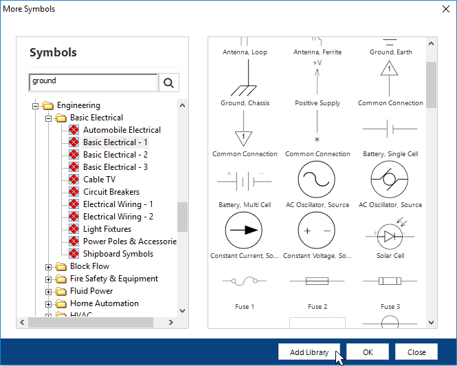
If you need more symbols, click on the Symbols tab and pull down the More menu. There are three different electrical symbol libraries already docked, but you can also search SmartDraw's entire symbol collection by clicking on More Symbols. If you find a library you want to add, click on Add Library. Keep adding as many libraries as you want. Close the search window when you're done to return to your drawing area.
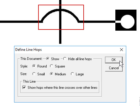
Line Hops
Click on Set Line Hops in the SmartPanel to show or hide line hops at crossover points and to change the size and shape of your line hops. Select Show Dimensions to show the length of your lines or the area of your shapes. Just select Add Text to type measurements and notations into your diagram.
Other Electrical Diagram Types
Wiring diagrams function very much the same way but employ a different set of symbols. Click more in the symbol library drop down menu and there are even more electrical symbols to choose from. Block diagrams, often used for higher level, less detailed descriptions for understanding overall concepts, use the same easy drawing tools and are easy to adjust and customize. A panel diagram is another handy visual. Just drag the many circuit breakers and panel components to where you want them to go and they anchor neatly into place.
Using Layers to Create Electrical Plans
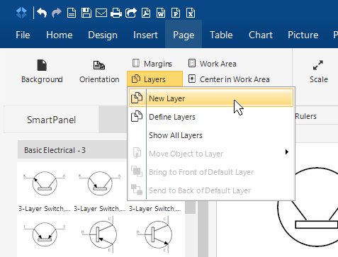
You can easily create detailed electrical plans by overlaying electrical symbols on a floorplan. Just open your floorplan and under the Page tab, choose Layers->New Layer. Name the new layer. You now have a separate layer on which to build your electrical plan. Look for the relevant electrical symbols in the Symbols tab, under More and More Symbols. Dock any libraries you may need using the Add Library command. Then just drag the symbols to where they belong on the floorplan. You can switch back and forth between the electrical and floorplan layers and choose to make a layer clickable or not clickable to protect the work that you've already done (and visible or not visible). This helps make your electrical plans easier to build, manage and share with others.
With SmartDraw's quick-start templates, extensive symbol libraries and intuitive drawing and formatting, you'll be making great looking electrical diagrams in no time.
Concepts and terminology used in Printed Circuit Boards (PCB)
Basic PCB Concepts
What is a printed circuit board?
A printed circuit board or PCB, is a plate or board used for placing the different elements that conform an electrical circuit that contains the electrical interconnections between them.
The most simple printed circuit boards are the ones that contains copper tracks or interconnects only on one of its surfaces. These kinds of boards are known as 1 layer printed circuit board or 1 layer PCB.
The most common PCB's manufactured today are the ones that contain 2 layers, that is, you can find interconnects in both surfaces of the board. However, depending on the physical complexity of the design ( PCB layout ), the boards can be manufactured of 8 or more layers.
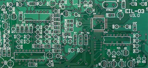
Fig 1. Example region of a 2 layer PCB
Soldermask
For mounting the electrical components on the printed circuit boards, an assembly process is required. This process can be done by hand or through specialized machinery. The assembly process requires the use of solder to place the components on the board. For avoiding or to prevent the solder to accidentally short-circuit two tracks from different nets, pcb manufacturers apply a finish or varnish called soldermask on both surfaces of the board. The most common color of soldermask used in printed circuit boards is green, followed by red and blue.
In EDA software (Electronic design automation), generally exist a rule associated to the expansion of the soldermask. This rule specifies the distance that exists between the pads' borders and the soldermask's border. This concept is illustrated in figure 2 (a).
Silkscreen or Overlay
Silk-screening is the process where the manufacturer prints information on the soldermask conducive to facilitate the processes of assembly, verification and repair. Generally the silkscreen is printed for indicating test points as well the position, orientation and reference of the electronic components that are part of the circuit. Also it can be used for any purpose that the designer may require, for example, the company name, configuration instructions (this was commonly used in old PC motherboards), etc. The silkscreen can be printed on both surfaces of the board. Also the term silkscreen is known as overlay. Figure 2 shows a region of a circuit, all the printings made in white correspond to the silkscreen.
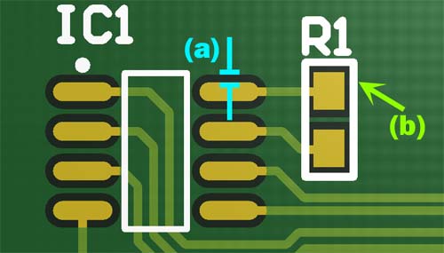
Fig 2. Soldermask expansion (a) and silkscreen (b)
Layer Stackup
As noted before in the beginning of this article, the printed circuit boards can be made of several layers. When a PCB is designed with the aid of an EDA software, often are specified several layers that doesn't necessary correspond to conductive material ( copper ). For example, the silkscreen and soldermask are nonconductive layers. Having conductive and nonconductive layers may lead to confusion, because manufacturers use the term layer when they are referring to the conductive layers only. From now on, we are going to use the term layer without the suffix "CAD" only when referring to conductive layers. If we use the term "CAD Layer" we are referring to all kinds of layer, that is, conductive and nonconductive.
The CAD Layer stackup is the following:
CAD Layer (conductive and nonconductive) | CAD Layer description |
| 1 | Top silkscreen/overlay ( nonconductive ) |
| 2 | Top soldermask ( nonconductive ) |
| 3 | Top paste mask ( nonconductive ) |
| 4 | Layer 1 ( conductive ) |
| 5 | Sustrate ( nonconductive ) |
| 6 | Layer 2 ( conductive ) |
| ... | ... |
| n-1 | Sustrate ( nonconductive ) |
| n | Layer n ( conductive ) |
| n+1 | Bottom paste mask ( nonconductive ) |
| n+2 | Bottom solder mask ( nonconductive ) |
| n+3 | Bottom silkscreen/overlay ( nonconductive ) |
Figure 3 shows 3 different stackups. The orange color highlights the layers in each stackup. The stackup height, or board thickness can vary depending on the application, however the most used is 1.6 [mm] or 62 [mils]. In some countries [thou] is used as a synonym for [mils]. ( 1 [mil] = 0.001 [inch] = 0.0254 [mm] )
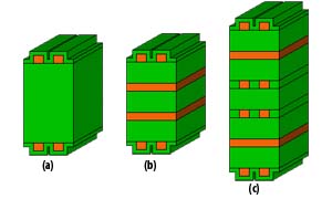
Fig 3. Example of 3 different PCB stackups: 2 layers (a), 4 layers (b) and 6 layers (c)
Component packages
Today in the market you can find a great variety of electronic component packages. It is common to find several types of packages for one device. For example you can find the same integrated circuit in QFP's and LCC's packages.
Basically there exist 3 big families of electronic packages:
| Package | Description | Example Image |
| Thru-Hole |
Are all those components that have pins intended to be mounted through a plated hole in the PCB. This kind of component is soldered to the opposite side of the board from which the component was inserted. Generally these components are mounted on one surface of the board only.
| 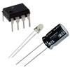 |
SMD/SMT (surface mount device/surface mount technology)
|
Are all those components that are soldered in the same side of the board from which the component was placed. The advantage of this type of package is that it can be mounted on both sides of the PCB. Also, these components are smaller than the thru-hole type, which allows the design of smaller and denser printed circuit boards. These types of components are useful for frequencies up to 200 [MHz] (fundamental clock frequency).
| 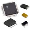 |
| BGA (Ball grid array) |
These types of components are frequently used for high density pin integrated circuits. For soldering them to the printed circuit boards it is required to have specialized machinery due that the pins are made of solder balls that have to be melted for making the electrical contact with the pads.
BGA components are ideal for high frequency integrated circuits due to the very small parasitic inductances present in the joint between the pad and the balls. These type of components are very common in computer hardware like motherboards and video accelerator cards.
| 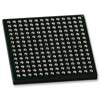 |
For more information you can visit this excellent article from wikipedia.
Pads
A pad is a small surface of copper in a printed circuit board that allows soldering the component to the board. You can think of a pad as a piece of copper where the pins of the component are mechanically supported and soldered. There are 2 types of pads; thru-hole and smd (surface mount).
Thru-hole pads are intended for introducing the pins of the components, so they can be soldered from the opposite side from which the component was inserted. These types of pads are very similar to a thru-hole via.
The smd pads are intended for surface mount devices, or in other words, for soldering the component on the same surface where it was placed.
Figure 4 depicts 4 components. The components IC1 and R1 have 8 and 2 SMD pads respectively, while both components Q1 and PW have 3 thru-hole pads.
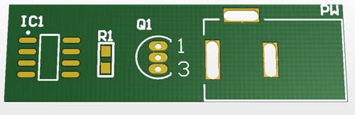
Fig 4. SMD and Thru-hole Pads
Copper tracks
A track is conductive path that is used to connect 2 points in the PCB. For example, for connecting 2 pads or for connecting a pad and a via, or between vias. The tracks can have different widths depending on the currents that flow through them.
It is important to highlight that in high frequencies is necessary to calculate the tracks' width so that the interconnect can be impedance matched along the path created by the track. ( more on this in a future article )
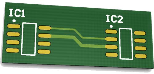
Fig 5. Tracks that interconnect 2 integrated circuits (chips)
Plated Holes (Thru-hole Vias or Full Stack Vias)
When an interconnect must be made from a component that is located on the top layer of the printed circuit board with another that is located at the bottom layer, a via (Vertical Interconnect Access) is used. A via is a plated hole that allows the current to pass through the board. Figure 6 depicts 2 tracks that begin at the pads of a component on the top layer and end at the pads of another component at the bottom layer. For conducting the current from the top layer to the bottom layer, a via is used for each track. The tracks and pads that belong to the bottom layer are visually dimmed, so you can differentiate them from the ones that are on the top layer.
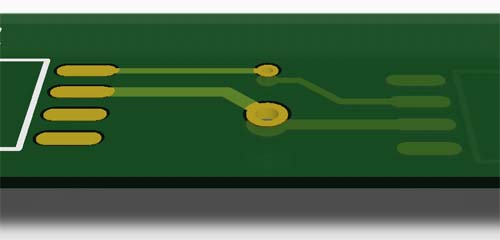
Fig 6. Two integrated circuits located on opposite sides of the PCB are connected using thru-hole vias
Figure 7 depicts a more detailed view of a transversal section of a 4 layer printed circuit board or 4 layer PCB. The colors that appear in the Figure are explained in the following table:
| Color | Legend for Figure 7 |
| green | Top and bottom soldermasks |
| red | Top layer ( conductive ) |
| violet | Second layer. In this case this layer is used as a power plane ( i.e. Vcc or Gnd ) |
| yellow | Third layer. In this case this layer is used as a power plane ( i.e. Vcc or Gnd ) |
| blue | Bottom Layer ( conductive ) |
The PCB depicted in figure 7 shows a track that belongs to the top layer that goes through the board using a thru-hole via, and then continues as a track that belongs to the bottom layer.
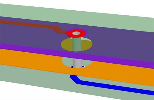
Fig 7. Track from the top layer going through the PCB and ending on the bottom layer
Blind vias
In high density complex designs is necessary to use more than 2 layer as we have shown in figure 7. Generally in multilayer system designs where there are many integrated circuits, power planes ( Vcc or gnd) are used to avoid excessive routing for power rails. In other words, it is lot easier and more secure to directly connect to the power planes that are beneath the chips instead of routing long tracks for the PDS ( Power Delivery System ) ( this can also be achieved with thru-hole vias ). Also there are times that a signal track must be routed from an external layer ( top or bottom ) to an internal layer with minimum via height because it can act as a stub and maybe produce an impedance mismatch. This can cause reflections and produce signal integrity issues ( more on this in a future article ). For these kinds of interconnects blind vias are used, which allows a connection to be made from an external layer to an internal layer with minimum via height. A blind via starts on an external layer and ends on an internal layer, that's why it has the prefix "blind".
To know if a certain via is blind, you can put the PCB against a source of light and see if you can see the light coming from the source through the via. If you can see the light, then the via is thru-hole, otherwise the via is blind.
It is very useful to use these kinds of vias in printed circuit board design when you don't have too much space for placing components and routing. You can put components on both sides and maximize the space. If the vias were thru-hole instead of blind, there would be some extra space used by the vias on both sides.
Figure 8 depicts 3 vias that are part of 4 layer printed circuit board. If we see the picture from left to right, the first via that we will see is thru-hole via or fullstack via. The second via begins at the top layer and ends at the second layer ( inner ), so we say that this is a 1-2 blind via. At last, the third via begins at the bottom layer and ends at the third layer, so we say that this is a 3-4 blind via.
It is important to have in mind that blind vias are often manufactured in consecutive layers, in other words between L1 L2, L3 L4, Ln-1 Ln.
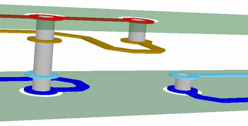
Fig 8. Comparison between a Thru-hole and a Blind via
The disadvantage of this type of via is its high price when compared to the thru-hole alternative.
Buried Vias
These vias are similar to the blind ones, with the difference that they begin and end on an inner layer. If we look at the image depicted in figure 9 from left to right, we see that the first one is a thru-hole or full stack via. The second one is a 1-2 blind via, and the last one is a 2-3 buried via that begins on the second layer and ends on the third layer.
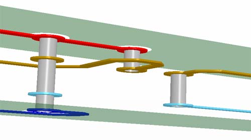
Fig 9. Comparison between Thru-hole vias, Blind vias and Buried vias
It is important to have in mind that blind vias are often manufactured in consecutive layers (i.e. L1 L2)
As the case of blind vias, the main disadvantage of this type of via is its high price when compared to the thru-hole alternative. Using b/bb vias may impact the cost of the boards in an important way, so you decide if it's better to use these kinds of vias or use bigger boards with thru-hole type vias.

If you have even a little bit of interest in learning about electronics, then you absolutely need to know about the printed circuit board or the PCB. Why? These boards are in every piece of electronics known to man, no exceptions! Open your computer, smartphone, or even a fork, and you’ll find a PCB.
The mighty PCB in items as common as a fork!
To the electronics beginner, these green shapes can seem a bit mysterious at first. There’s a ton of different looking parts, and plenty to learn to know how it all works together. But with a high-altitude perspective, understanding what a PCB is and how it works can be easy. Look at a PCB from 10,000 feet, and you’ll find that it looks just like a city!
I Can See Clearly Now
You’ve likely flown in an airplane at least once in your life. My favorite part of the journey is when the plane takes off from the runway. As you climb higher and higher, you get a new perspective on a city that you only see from the great heights. And the higher you go, the more you start to see just how your city is organized and meticulously planned. There’s roads, buildings, cars, and people all connected in a complete system.
Los Angeles at night with its grid-like layout. Keep this in mind as you learn about all of the parts of a PCB!
Just like our cities, circuit boards provide a complete system, a foundation, for all of the electronic components that make our objects come to life. In fact, you can compare many aspects of a city to a PCB, like:
Roads & Cars
On a PCB you’ll notice a bunch of lines running all over the place, connecting to various components. These are just like the roads in our cities, except instead of cars zipping around, electrons are flying down roads made out of copper, hurrying off to power one component after another! These copper roads are called traces in our PCB city.

A PCB without any of its components, you can see the traces going all over the place.
Downtown
Downtown is where all of the work in a city happens. You’ve got your big corporate offices, local business on every corner, and maybe even some open markets. This central hub of human activity is just like those square black shapes that you’ll find on a PCB called Integrated Circuits (ICs). These ICs are where all of the tough work happens in a PCB, doing rapid-fire calculations.
Pull out a PCB, and you’re bound to find an integrated circuit at the heart of it. Just look for the black square or rectangular boxes!
Suburbs
In the suburbs are where homes, parks, and schools are a common sight. From a plane, you’ll notice that the rows of houses in a suburb often look just like the small resistors found all over a PCB. These resistors are out there resisting the flow of electricity according to their value.
Resistors are super tiny on today’s modern electronics. Here are two close up.
Construction
No city is free from construction! Whether it’s building a new skyscraper or a new apartment complex, you’ll find new foundations being laid everywhere. These foundations are just like the empty pads that you’ll find on a PCB with no components on it. While they might be empty now, a component will soon be soldered to them.
See all of those empty metal shapes; those are connection points for components.
Addresses & Street Names
You won’t find your way around a city without some address or street name. And just like how these two help you to navigate mazes of streets, all of the white writing that you find on a PCB does just the same. This lettering, called silkscreen, helps people that are assembling or fixing PCBs to know exactly what a part is and its location.
Silkscreen up close, you can see some that identify capacitors by C2, C3, and C4, and a diode by D1.
Sewer System
All of that water that we use when doing the dishes or washing our car has to go somewhere, and into the sewers it finds itself traveling to new destinations. The sewer system is just like the holes you might find on a PCB called vias. These manhole-like shapes help to deliver electricity from one side of a PCB to another, just like how water travels from your sink to the local sewage plant, it’s an expressway!

Vias are the tiny holes you’ll see on some PCBs, allowing electricity to other layers.
Power Plant
Power plants keep our lights running. Could you imagine what a city would be like without any? Hopefully, not zombie infested! Just like power plants in a city, we have what are called capacitors on a PCB that store electricity. They can hold a charge, and release it when needed to send power where it needs to go.
A ton of capacitors all lined up. Notice the unique cylindrical shape. Most capacitors will look like this.
Street Lights & Signs
Street lights and signs help to keep order in a world full of crazy drivers, controlling the flow of traffic in our maze of streets and highways. On a PCB, streetlights, and signs are just like diodes and their cousin the LED. The diode controls the flow of electricity on a PCB, allowing it to go only in one direction. And you’re bound to have seen a LED, it’s just like a diode, except that it lights up when electricity runs through it.

Two diodes on a PCB, controlling the flow of electricity. (Image source)
Now that you have all the individual parts put together in your mind check out the picture below to see if you can point out some of the landmarks on this here PCB. Integrated circuits are the easiest to find, just look for the black boxes. But you might need to squint to see all of the tiny resistor suburbs grouped all over the place. Of course, the parts and pieces we listed above are only a fraction of the things you’ll find on a PCB, but you’ve got enough knowledge now to yank the PCB out of any piece of electronics and start naming things!

Can you spot some of the parts we talked about on this completed PCB? They’re everywhere!
How would I make a PCB?
You can think of a PCB as a kind of delicious, multi-layered vanilla and strawberry cake when looked at from the side. It has several repeating layers of copper, solder mask, silkscreen, and fiberglass. Let’s start from the inside out to understand these layers.

A cross section of a double-sided PCB with silkscreen, solder mask, copper, and FR4. (Image source)
Fiberglass. This material rests at the center of a PCB and is commonly referred to as a substrate, or FR4. The fiberglass is the strongest layer of them all and is responsible for giving a PCB it’s rigid and thick structure. When making a PCB, the entire process starts with the fiberglass, and all the other layers are added on top.
Copper. Without a layer of copper, a PCB would never be able to conduct electricity. You’ll usually find copper on both the top and bottom of a PCB, and it contains all of the traces that will connect your components.
Soldermask. This stuff is what gives a PCB its traditional green color and is applied over the copper layers. You might also find PCBs in red or blue; it’s the designer’s choice! Solder Mask holds an outstanding job of keeping all of the copper traces insulated from each other so no accidents can occur like short circuits.
Silkscreen. You’ll find this white text all over the place on a PCB, identifying the names of resistors, capacitors, LEDs, etc… Silkscreen comes in handy when you’re making a PCB, as it can tell another human or computer where a particular part needs to go.
The actual process of how a PCB is made can be complicated, and involves the use of a manufacturer, also called a fab house by some. These fab houses will take all of the completed design files that an engineer hands off to create a PCB in its physical form. While the entire process is deserving of its own blog post, we’ll keep things simple with a brief outline of how a PCB comes to be:
- Step 1 – Creating a fiberglass foundation. A manufacturer will first make the inner fiberglass layer (core) that all of the other layers of copper, solder mask, etc.. will be applied to.
- Step 2 – Adding copper layers. With the fiberglass foundation in place, a manufacturer will then add copper foil on both sides of the fiberglass.
- Step 3 – Adding copper patterns. Next, a laminated sheet of the PCB design is laid on top of the copper, which shows where all of the copper traces need to be.
- Step 4 – Defining copper patterns. The laminated sheet and copper are then exposed under a UV lamp and covered with a photoresist film, which etches the traces into the copper foil.
- Step 5 – Bathing the board. Now that the copper traces are in place, a PCB will then be given a chemical bath that removes all of the unwanted copper, leaving only the copper traces that an engineer designed.
- Step 6 – Protecting with solder mask. A protective layer of solder mask is applied, giving a PCB its traditional green color while protecting it from short circuits.
- Step 7 – Adding silkscreen. To finish up, white silkscreen is added which will help to know exactly where components need to go on a PCB. At this stage, the PCB is considered complete as a “bare board,” meaning it has no parts attached yet.
- Step 8 – Adding components. The bare board is then taken through an assembly process where various components like resistors, integrated circuits, capacitors, etc. are attached. Once complete, this is the PCB in its final form that you’ll see in all of your electronics at home.
The assembly process has quite a few details that we left out and is a world in itself. If you’re interested in learning more about the manufacturing process, be sure to check out the video below to see it in action at Eurocircuits!
Were PCBs Always This Complex?
The green PCBs that we have come to know in all of our electronics have not always been so. Why, just over 60 years ago, you were bound to see PCBs made from materials like masonite, cardboard, and even wooden planks. In these old-school PCBs, flat brass wires were bolted onto the board, and a collection of components were scattered all over the place. Here’s an old TV with one of the earliest PCBs inside, look at that mess!

Look at that mess! Here’s an old-school PCB in a TV before modern copper boards were invented.
This monstrosity of a PCB soon changed, though, and in 1943 Austrian scientists Dr. Paul Eisler created the first modern PCB for a radio. Soon after, copper replaced brass the metal of choice for PCBs, as it allowed electricity to flow more efficiently and it was also a lot cheaper to manufacture.
The PCB finally got its moment of fame in 1956, when the US Patent Office issued a patent for the “Processing of Assembling Electrical Circuits” to a group of scientists in the US Army. It’s the military that is to be thanked for many of the advancements we’ve seen in PCBs. Thanks to their need for new weapons and communications systems, we’ve taken the hulking mass of PCBs of yesterday and shrunken it down into something that can fit into our pockets!
Today’s Wild and Crazy Uses for PCBs
Today, PCBs are all over the place, powering some of the wild and crazy gadgets and services that we could have ever imagined existing. Have you heard of these?
Delivery Drones
Amazon recently unveiled their new delivery service, Prime Air, made possible by drones! We’re talking about being able to order something off Amazon and have it delivered to your home in mere minutes, not days, all thanks to the power of PCBs.
The PCBs in these drones deliver all of the complexity needed to get the job done, including GPS and Bluetooth that allow a package to be delivered with precision, and gyroscopes and accelerometers that keep them flying straight. Check out the video below to see Amazon Prime Now in action.
Prosthetic Limbs
Gone are the days of plain mechanical limbs that didn’t provide any feedback. Today’s prosthetic limbs are packed with microprocessors that are adding a whole new level of natural experience. In prosthetic legs, knee angle sensors can provide information to a microprocessor about pressure adjustments in the heel or front part of the foot. This all leads to a much more natural walking experience thanks to PCBs and their microprocessor counterparts.
Hearing Implants
Cochlear Implants allows the deaf or hearing impaired to hear again all thanks to the power of PCBs and electronics. These implants are placed surgically under the skin and contain a ton of electronics, including:
- A microphone that picks up all the variety of sounds from an environment.
- A speech processor that can make sense of all the sounds collected by the microphone.
- A transmitter, receiver, and stimulator that receives signals from the speech processor and converts them into electrical impulses.
- An electrode array which collects all of the electrical impulses from the stimulator and sends them to regions of the auditory nerve to be heard!
These are just a few of the extraordinary uses that PCBs and electronics as a whole have made possible for the human race. There’s a ton more out there, like the computer or smartphone that you’re reading this blog post on. Without a PCB, you would never be here! Or how about the craziness of the SpaceX self-landing rocket? Hats off to you again, PCB.
To Infinity, and Beyond
The PCB is the foundation to our future, allowing us to create, discover and improve the human experience in ways we might have never thought possible. But today, we’re just at the beginning of our journey with PCBs. In the future, we might find ourselves using biodegradable circuit boards to help eliminate electronic waste. Or perhaps you’ll be able to 3D print your own PCB from the comfort .
XO__XO XXX Fully printed electronics on flexible substrates: High gain amplifiers and DAC
Graphical abstract

1. Introduction
The printing technologies for printed electronics can in general be classified as either ‘Subtractive’ or ‘Additive’ processes. Subtractive-based processes, including Laser Ablation and Photolithography , are presently dominant, and largely resembles and leverages on present-day conventional silicon-based processing, involving a series of additive (deposition) and subtractive (etching, lift-off, etc.) steps. The primary shortcoming of this process is the complexity of the steps thereof – they involve highly specialized processing (and associated expensive/sophisticated equipment and infrastructure), including the use of corrosive chemicals for the subtractive steps. Not unexpectedly, the ensuing Subtractive-based printed electronics is un-green (use of corrosive chemicals), not-on-demand, un-scalable (printing sizes are limited to wafer-size due to the specialized equipment, e.g. 200 mm and 300 mm), and high-cost (including high wastage of chemicals, in part due to etching/lift-off, etc.). In this sense, Subtractive-based printed electronics somewhat contravene the often-touted merits of printed electronics: green, on-demand, scalable and low-cost.
At this juncture, several Fully-Additive processes have been reported , where the steps strictly involve depositions only (without etching or lift-off) – each printed layer is deposited on layer-upon-layer to realize transistors, passive components (resistors, capacitors and inductors) and interconnections thereto. It is instructive to note that the denotation ‘Fully-Additive’ used herein explicitly stipulates that all processing steps in the process are strictly depositions. There is somewhat a misnomer to the denotation ‘Additive’ because several reported processes e.g. were inadvertently deemed ‘Additive’ when some of the printing steps therein are subtractive. Not unexpectedly, in these processes, some of the same aforesaid shortcomings of Subtractive-based processes apply. Reported hitherto Fully-Additive-based printed electronics are uncompetitive when compared to their Subtractive-based counterparts due their low printed semiconductor carrier-mobility, thereby further and severely limiting the ensuing applications to even lower speed.
In this paper, we propose a Fully-Additive printing process that circumvents the aforesaid shortcomings of state-of-the-art Fully-Additive processes, rendering the ensuing Fully-Additive printed circuits/systems competitive to Subtractive-based processes in terms of carrier-mobility and the ability to print complex circuits/systems including transistors, passive components (capacitors, resistors and inductors) and two metal-interconnect layers on flexible substrates (such as plastic films, e.g. polycarbonate film ). Hence, the ensuing printed electronics from the proposed Fully-Additive printing process feature the aforesaid often-touted merits of printed electronics. The proposed process features the ability of realizing complex circuits/systems on flexible plastic films – hence highly competitive to the substantially more complex and expensive Subtractive-based processes. The printing herein is a screen printing process similar to that ubiquitously used for printing multiple-colored prints on tee-shirts, and the equipment and facilities used are largely the same (save the chemicals and curing steps) – low-cost and unsophisticated. The proposed Fully-Additive printing process features high semiconductor carrier-mobility (∼1.5 cm2/Vs, which is ∼3× higher than state-of-the-art; see Table 2 later) and capable of printing passive components (capacitors, resistors and inductors), and two metal-interconnect layers. The range of the values of the printed capacitors, resistors and inductors are large: respectively 224 pF/cm2to 1.1 nF/cm2, 3.3 kΩ/□ to 800 kΩ/□ and 1 μH to 8 μH with quality factor Q of 2; Q of 2 is sufficient for many applications, including RFID. These large ranges are desirable for sake of generality for the efficacious design and realization of analog and mixed-signal circuits/systems.
Table 1
| Layers | Materials | Printing procedure |
|---|---|---|
| Layer 0: Substrate (flexible plastic film) | Polycarbonate | Clean the substrate to remove contaminants |
| Layer 1: Gate, bottom electrode of capacitors, inductor | Silver | With the first stainless screen mask (400 mesh count), print the pattern of Layer 1, and then cure in an oven at 120 °C for 10 min |
| Layer 2: Dielectric of transistors and capacitors, isolation between top and bottom interconnections | Dupont 5018 | With the second stainless screen mask (400 mesh count), print the pattern of Layer 1, and then cure in the UV light with speed of 5ft/min at the power of 350 W/inch2 |
| Layer 3: Resistor | Dupont 5036 , Dupont 7082 | With the third stainless screen mask (200 mesh count), print the pattern of Layer 3, and then cure in an oven at 120 °C for 10 min |
| Layer 4: Drain, source, top electrode of capacitors, vias, interconnections | Silver | With the fourth stainless screen mask (325 mesh count), print the pattern of Layer 4, and then cure in an oven at 120 °C for 10 min Immerse into the PFBT (pentafluorobenzenethiol) solution for 1 h |
| Layer 5: Semiconductor | TIPS-Pentacene | Coat layer 5 using the slot die coater with speed of 0.1 mm/s and then cure in an hotplate for 30 min at 90 °C |
Table 2
| Channel length (μm) | Printing technology | Mobility (cm2/Vs) | Vth (V) | Circuits | VDD (V) | |
|---|---|---|---|---|---|---|
| This work | 100 | Screen printing and slot die coating | 1.5 | 0 | Diff amps and DAC | 60 |
| [3] | 50 | Inkjet printing | 0.02 | −1.2 | Inverter | 60 |
| [4] | 70 | Flexography and gravure printing | p: 0.0039 n: 0.0029 | p: −1.5 n: −1 | Ring oscillator | 100 |
| [5] | 140 | Inkjet, drop casting and evaporation | p: 0.0078 n: 0.0037 | N.A. | – | 80 |
| [6] | 50 | Aerosol jet printing | N.A | 0.25 | – | 2 |
| [7] | N.A. | Inkjet printing | 0.0035 | −3.85 | – | 30 |
| [8] | 20 | Inkjet printing | 0.053 | −7.8 | – | 60 |
| [9] | 12.6 | Gravure and flexography with PDMS stamp | 0.1 | −3.54 | – | 20 |
| [10] | N.A. | Inkjet printing | 0.45 | 10.5 | – | 60 |
| [11] | 5 | Inkjet printing and spin coating | 0.25 | 1.3 | – | 40 |
| [12] | 200 | Gravure printing | 0.03 | −3 | 1-bit RFID tag | 10 |
| [13] | 100 | Flexography and gravure printing | 0.004 | N.A | Ring oscillator | 60 |
On the basis of the proposed Fully-Additive screen printing process, three fundamental analog (a proposed and two conventional differential amplifiers) circuits and a mixed-signal (4-bit digital-to-analog converter (DAC)) circuit are demonstrated. Of specific interest in terms of circuit design, we propose to employ a novel positive-cum-negative feedback for the proposed amplifier to simultaneously improve the gain (>14 dB higher than the conventional Fully-Additive three-stage amplifier of equivalent hardware and printed area), and mitigate the effects of process variations (reduced to 5% of the Fully-Additive conventional amplifiers). The 4-bit DAC, on the other hand, is competitive to the state-of-the-art Subtractive-based DAC (realized on plastic film) in terms of supply voltage and resolution; speed would also be competitive if the channel length is scaled accordingly. Overall, we show that despite our analog and mixed-signal circuits realized by means of a Fully-Additive process, they are highly competitive when compared to reported circuit counterparts based on the substantially more complex and expensive Subtractive-based processes.
2. Fully-additive printing technology
The overall spirit of the proposed screen printing process is low-cost and simplicity (including processing steps, chemicals used, and the associated equipment (and infrastructure)), yet high performance (in terms of high carrier-mobility, capability to print complete circuits/systems on plastic films, and in terms of ensuing circuits/systems parameters) when compared to the substantially more expensive and complex state-of-the-art Subtractive-based processes.
The adopted structure of the printed transistor is the conventional bottom-gate-bottom-contact structure depicted in the top left of Fig. 1(a). The materials/chemicals are readily available, and process is low temperature, <120 °C. The associated equipment and infrastructure are also simple, including a screen printer, an ultra violet (UV) light source and a slot die coater. The proposed printing method encompassing the printing of Layers 0–5 is summarized in Table 1 below.

Fig. 1
The typical input–output and output characteristics of our printed p-type transistor are depicted in Fig. 2. The Fully-Additive printed transistor has a carrier mobility of ∼1.5cm2/Vs with a standard derivation of 4.56%, threshold voltage (Vth) = 0 V, and Ion/Ioff ratio = 105. This carrier-mobility is very significantly increased from ∼0.03cm2/Vs (reported screen printing methods ), and the highest carrier-mobility of all Fully-Additive processes to-date, see Table 2. The high Ion/Ioff ratio is desirable for realizing robust digital circuits/systems

Fig. 2
To circumvent the severe low carrier-mobility problem, we propose two innovations. The first innovation involves modifying the electrode-semiconductor interface. In our process, silver is used as the electrode material largely because screen-printable silver paste is readily available and its electrical and thermal conductivities are high. However, a major drawback of silver is its low work function, ΦAg = 4.7 eV. Specifically, as the HOMO (highest occupied molecule orbital) of TIPS-Pentacene (ΦTIPS-PEN = 5.28 eV) is relatively high and ΦAgrelatively low, the overall work function is poorly matched, resulting in high injection barrier, hence low carrier-mobility. To mitigate this mismatch, we propose to increase the silver work function by immersing the printed drain and source into PFBT (pentafluorobenzenethiol) solution. This PFBT treatment increases the silver work function from ΦAg = 4.7 eV to ΦAg = 5.35 eV, a level in the vicinity of ΦTIPS-PEN.
The second innovation involves a proposed printing step for the semiconductor. Specifically, we propose the use of the slot die coater instead of the reported inkjet , spin coating , drop casting , etc. to print the TIPS-Pentacene semiconductor layer. It is interesting to note that although slot die coating is commonly used for printing the active materials for solar cells, to our knowledge, this is the first application for printed transistors . The advantage of using a slot die coater is that the crystal formation of the TIPS-Pentacene is well controlled by the coating direction so that the crystal grain boundaries are decreased, thereby facilitating the flow of electrons between the source and drain of the transistor.
Passive elements (resistors, capacitors and inductors) can likewise be Fully-Additive printed, and all circuit elements interconnected by at least two metal-interconnect layers. In the case of resistors, we use a blend of high (Dupont 5036 ) and low (Dupont 7082 ) resistivity materials to obtain a reasonably large range of printed resistor resistivities. By means of this composition blending, the ensuing resistivities of the printed resistors range from 3.3 kΩ/□ to 800 kΩ/□.
In the case of capacitors, a large range of capacitances is likewise desirable. To obtain this, we employ a multiple dielectric-layer structure, similar to the double MIM-cap in silicon processes . Fig. 3 depicts the cross-section of a Fully-Additive triple dielectric-layer (four metal layers) printed capacitor. Depending on the number of dielectric layers, the capacitance ranges from 224 pF/cm2 (for single dielectric-layer) to 1.1 nF/cm2 (for quintuple dielectric-layer).

Fig. 3
In the case of Fully-Additive inductors, the inductance ranges from 1 μH to 8 μH with Q = 2 at 10 MHz. Although the Q factor is relatively low, the printed inductor is nevertheless sufficient for many applications, including the 13.56 MHz RFID.
3. Fully-Additive printed analog and mixed-signal circuits
In this section, several printed analog and mixed-signal circuits based on the proposed Fully-Additive process are demonstrated, including a proposed and two conventional differential amplifiers, and a DAC.
3.1. Fully-Additive printed differential amplifiers
The general desirable attributes of an amplifier include high gain and high gain-bandwidth. In the context of printed electronics, amplifier designs are challenging because of the low semiconductor carrier-mobility (>103× lower than silicon), absence of n-type transistors (particularly for Fully-Additive processes and in most Subtractive-based processes), and high process variations; due to the absence of n-type transistors, established gain-boosting methods such as cascode topologies used in silicon-based designs are inapplicable here. Several reported gain boosting methods in printed electronics employ zero-VGS connected transistors (transistors in the cut-off region) as the active load. From a practical printed electronics perspective, this practice is avoided here because of the ensuing high sensitivity of the amplifier parameters (including gain and output common-mode voltage, etc.) to process variations – a serious drawback. This is because the impedance of zero-VGS connected transistors is very sensitive to process variations, largely due to poor matching. Thus diode-connected transistors are preferred to serve as the active load to overcome the process variations although the gain is degraded. Fig. 4 depicts the schematic, microphotograph, measured and simulated characteristics of a diode load inverter at supply voltage of 60 V, the maximum gain is ∼9 dB.

Fig. 4
To circumvent these challenges and drawback, we propose a differential amplifier embodying a novel positive-cum-negative feedback path. The positive feedback path serves to significantly increase the gain whilst the negative feedback path reduces the output common-mode sensitivity of the amplifier. It is interesting to note that positive feedback is usually avoided in silicon-based amplifier designs due to the increased possibility of instability. However, positive feedback herein is appropriate due to the low (relative to silicon) carrier-mobility (hence low gain) where the possibility of instability is virtually negligible.
Fig. 5(a–c) respectively depicts the schematic of the proposed single-stage, conventional single-stage and the conventional three-stage differential amplifiers. The microphotograph of the proposed and conventional single-stage differential amplifiers printed based on the proposed Fully-Additive process is depicted in Fig. 5d and e respectively, and the layout of the conventional three-stage amplifier is depicted in Fig. 5f. From Fig. 5(a–f), it can be seen that the conventional single-stage amplifier is the hardware simplest and as expected, its ensuing printed area (2.75 cm × 3.5 cm) is the smallest. On the other hand, the hardware complexity (in terms of transistor count) and printed area of the proposed single-stage and the conventional three-stage amplifiers are approximately the same: 12 transistors on 3.25 cm × 4.25 cm and 13 transistors on 3.25 cm × 5 cm for the proposed single-stage and conventional three-stage amplifiers respectively; their performance is however markedly different, see below.
Fig. 5
On the basis of measurements and simulations on the printed proposed and conventional single-stage amplifiers and of simulations on the conventional three-stage amplifier, Fig. 6(a–c) respectively depicts their time-domain responses, frequency responses, and output common-mode variations due to threshold voltage (process) variations. As the simulations and measured plots in Fig. 6a and b agree well, our derived SPICE models (for sake of brevity, not described herein) for our Fully-Additive printed transistors are precise.

Fig. 6
The proposed amplifier features two advantages over the conventional designs, particularly the exploitation of simultaneous positive-cum-negative feedback therein. First, from Fig. 6a and b, the gain of the proposed amplifier is ∼27 dB, and is significantly higher than that of the conventional three-stage and single-stage amplifiers, whose gain is ∼13 dB and ∼8 dB respectively. With respect to the conventional three-stage amplifier, this significantly higher gain is obtained largely without compromising the gain-bandwidth and without incurring hardware or printed area penalty. The functionality of the transistors in the proposed design in Fig. 5a is as follows. Two differential pairs with diode-connected load configuration are employed, comprising M7, M1, M4, M6 forming one pair, and M8, M2, M3, and M5 forming the second pair. M7, M8 are current biasing transistors, M1, M4, M2, M3 are input transistors, and M5, M6 are diode-connected load transistors of M3 and M4, respectively. The output of each differential pair (source of M5 and M6) is fed back to the current biasing transistor (M7 and M8) of another pair through a voltage level shifter (M9, M11 and M10, M12, respectively). The gain of the proposed amplifier AV can be easily derived as:
(1)
where gm1, gm5, and gm8 are respectively the transconductance of M1, M5 and M8.
Second, the application of negative feedback reduces the output common-mode voltage sensitivity of the amplifier to the process variations. For instance, when the output common-mode voltage (Vout1 and Vout2) increases due to process variations (e.g. threshold voltage variations), the source voltage of M9 and M10 (the gate voltage of M7 and M8) also increases, thereby reducing the current in M7 and M8 and consequently, reducing Vout1 and Vout2. Conversely, when Vout1 and Vout2 reduce due to process variations, the negative feedback will pull up Vout1 and Vout2. On the basis of simulations, Fig. 6c compares the output common-mode variations as a function of threshold voltage variations of the proposed and conventional signal-stage, and conventional three-stage amplifiers. It is apparent here that as a consequence of the embodiment of negative feedback, the output common-mode sensitivity to process variations of the proposed amplifier is significantly improved compared to the conventional amplifiers. As a case in point, for 5 V threshold voltage variation, the output common-mode variation for the proposed amplifier is a mere 0.3 V vis-à-vis 5.6 V and 6.5 V respectively for the conventional single-stage and three-stage amplifiers, equivalent to a significantly reduced 5% thereof.
To put the attributes of the proposed amplifier design in perspective, Table 3 benchmarks the proposed amplifier (Fully-Additive process) against reported state-of-the-art differential amplifiers (all based on Subtractive processes) on flexible substrates; note that amplifiers based on Fully-Additive process are not included as to the best of our knowledge, they are hitherto unreported. It is apparent from this table that the proposed amplifier features a high gain despite its realization based on the proposed simple low-cost Fully-Additive process. Further, the reported relatively high gain amplifiers are based on zero-VGS connected load, which as delineated earlier, are disadvantageous as they are very sensitive to process variations. Nevertheless, although the bandwidth of the proposed amplifier is somewhat modest due to the low-cost ‘tee-shirt’ printing equipment, the proposed amplifier remains highly competitive for printed electronics.
Table 3
| Printing technology | Channel length (μm) | Load configuration | Gain (dB) | Bandwidth (Hz) | ||
|---|---|---|---|---|---|---|
| This work | Fully-Additive Process | Screen printing and slot die coating | 100 | Diode connected | 27 | 70 |
| [1] | Subtractive Process | Laser ablation and screen printing | 20 | Complementary configuration | 22.4 | 1025 |
| [22] | Photolithography and vacuum evaporation | 10 | Zero-VGS connected | 18.6 | N.A. | |
| [23] | Photolithography and vacuum evaporation | 5 | Bootstrapped zero-VGS connected | 18 | 600 | |
| [24] | Photolithography and vacuum evaporation | 5 | Zero-VGS connected | 23.5 | 7.5 | |
| [25] | Photolithography and vacuum evaporation | 5 | Diode connected | 10 | 1400 | |
| [26] | Laser ablation and screen printing | 20 | Complementary configuration | 50 | 75 |
3.2. Fully-Additive printed digital to analog converter
We further demonstrate the feasibility of realizing a Fully-Additive printed mixed-signal circuit, embodying both analog and digital circuits, passive elements (capacitors) and two metal-interconnect layers. Fig. 7a and b respectively depicts the schematic and microphotograph of the 4-bit DAC whose architecture is based on the well-established binary-weighted charge-redistribution architecture. This architecture is chosen for its hardware simplicity (low transistor count) and independence of transistor matching (instead, capacitor-matching dependent); note that the matching of printed capacitors is more precise than printed transistors.

Fig. 7
There are two major design challenges in the DAC design. First, the low operation speed due to the low semiconductor carrier-mobility, and second, the large parasitic capacitance associated with the printing process, particularly when the capacitors is a single-dielectric layer capacitor; for sake of printing simplicity, we adopt the single-dielectric layer capacitor here. In this case, the specific capacitance (capacitance per unit area) of C1–C4 in Fig. 7a and the parasitic capacitance of printed transistors and that due to the overlap of the top and bottom interconnections is largely the same. In this first realization, the binary weighted capacitors are realized simply by scaling their sizes herein; scaling by means of multiple unit-sized capacitors will be described in a separate paper.
To mitigate these two design challenges, we propose to exploit some of parasitic capacitors so that the capacitors used herein are minimal. Specifically, the three parasitic capacitors between Buffer and Gnd nodes, as depicted in Fig. 7b, are exploited to collectively function as C5 in Fig. 7a. The other capacitors (C1–C4) are thereafter scaled in size accordingly. In this fashion, the ‘free’ (parasitic) capacitances are not only exploited but define the minimum capacitance for the binary-weighted capacitor array; the ‘usual’ alternative is a deliberate C5which would otherwise need to be scaled to be much larger than the parasitics, thereby resulting in a substantially larger overall capacitor array. As the consequent capacitors in the DAC are now relatively small, the required printed area is reduced and speed of the DAC improved. For completeness, note that the drawbacks nevertheless are the larger clock feedthrough (due to the large parasitic capacitors of the transistor switches, M1–M8 and Inv1–Inv4), a small DC offset and gain error (due to the parasitic capacitor of the reset transistor, Mreset). These drawbacks are, nevertheless, inconsequential as the clock feedthrough has little effect on the steady-state output and the DC offset and gain error can be easily compensated by the subsequent blocks in the system embodying the DAC.
Fig. 8a depicts the measured output time domain waveform when the input sequentially increases from 0000 to 1111. Fig. 8b depicts the measured transfer function characteristics, and the Differential (DNL) and Integral Non-Linearities (INL) for 5 Hz, 100 Hz and 300 Hz sampling rate. The DNL and INL for 5 Hz, 100 Hz and 300 Hz is −0.8LSB (Least Significant Bit) and 0.4 LSB; 0.6 LSB and −1.0LSB; and 0.8LSB and 0.9LSB respectively.

Fig. 8
To put the attributes of the proposed DAC in perspective, Table 4 benchmarks the proposed DAC based on the proposed Fully-Additive process (to our knowledge, the only DAC that is Fully-Additive printed) against the reported DAC on flexible substrates (based on Subtractive process); only one DAC on a flexible substrate (others are on glass and are hence not benchmarked here) has thus far been reported. A comparison against the reported DAC shows that our proposed DAC is competitive in terms of resolution and supply voltage, but disadvantages in terms of speed. This disadvantage is largely due to the large channel length, a consequence of the imprecise registration (alignment between masks) and the low-cost ‘tee-shirt’ equipment.
Table 4
| Printing technology | Channel length (μm) | Resolution (Bits) | VDD (V) | Speed (S/s) | ||
|---|---|---|---|---|---|---|
| This work | Fully-additive process | Screen printing and slot die coating | 100 | 4 | 30 | 300 |
| Subtractive process | Photolithography or laser ablation and screen printing | 20 | 4 | 40 | 8.4 k⁎ |
- ⁎
- Unspecified in , estimated based on the Ref. by the same authors.
4. Conclusions
A printing process, embodying simple depositions-only processing steps, for realizing printed electronics circuits/systems on flexible substrates has been proposed. Specifically, the process is Fully-Additive (vis-à-vis Subtractive-based processes embodying complex deposition-cum-etching steps) – green, on-demand and low-cost. This process is not only uniquely capable of printing the semiconductor of transistors with high carrier-mobility (∼1.5cm2/Vs, equivalent to 3× higher than reported Fully-Additive processes, and comparable to Subtractive-based process), but unique amongst Fully-Additive process because of its capability to print passive elements (capacitors, resistors and inductors) and two metal-interconnect layers, hence complete circuits/systems on flexible substrates. By means of the proposed Fully-Additive process, several analog and mixed-signal circuits have been demonstrated, including proposed and conventional single-stage differential amplifiers, conventional three-stage differential amplifier and a DAC. By means of a novel positive-cum-negative feedback path, the proposed amplifier has been shown to feature significantly higher gain and significantly lower susceptibility to process variations compared to conventional amplifiers realized using the same Fully-Additive process, and highly competitive to amplifiers realized using Subtractive processes. The performance of the DAC has also been shown to be highly competitive.
XO__XO XXX 10001 + 10 New media art
New media art refers to artworks created with new media technologies, including digital art, computer graphics, computer animation, virtual art, Internet art, interactive art, video games, computer robotics, 3D printing, cyborg art and art as biotechnology. The term differentiates itself by its resulting cultural objects and social events, which can be seen in opposition to those deriving from old visual arts (i.e. traditional painting, sculpture, etc.). This concern with medium is a key feature of much contemporary art and indeed many art schools and major universities now offer majors in "New Genres" or "New Media"[1] and a growing number of graduate programs have emerged internationally.[2] New media art often involves interaction between artist and observer or between observers and the artwork, which responds to them. Yet, as several theorists and curators have noted, such forms of interaction, social exchange, participation, and transformation do not distinguish new media art but rather serve as a common ground that has parallels in other strands of contemporary art practice. Such insights emphasize the forms of cultural practice that arise concurrently with emerging technological platforms, and question the focus on technological media, per se.
New Media concerns are often derived from the telecommunications, mass media and digital electronic modes of delivering the artworks involve, with practices ranging from conceptual to virtual art, performance to installation.


The origins of new media art can be traced to the moving photographic inventions of the late 19th century such as the zoetrope (1834), the praxinoscope (1877) and Eadweard Muybridge's zoopraxiscope (1879). From the 1920s through the 1950s, various forms of kinetic and light art, from Thomas Wilfred's 'Lumia' (1919) and 'Clavilux' light organs to Jean Tinguely's self-destructing sculpture 'Homage to New York' (1960) can be seen as progenitors of new media art.
In 1958 Wolf Vostell becomes the first artist who incorporates a television set into one of his works. The Black Room Cycle. This installation is part of the collection of the Berlinische Galerie.
During the 1960s the development of then new technologies of video produced the new media art experiments of Nam June Paik, and Wolf Vostell with the installation 6 TV Dé-coll/age in 1963 at the Smolin Gallery in New York. A. Michael Noll, and multimedia performances of E.A.T., Fluxus and Happening. In 1983, Roy Ascott introduced the concept of "distributed authorship" in his worldwide telematic project La Plissure du Texte[6] for Frank Popper's "Electra" at the Musée d'Art Moderne de la Ville de Paris. The development of computer graphics at the end of the 1980s and real time technologies then in the 1990s combined with the spreading of the Web and the Internet favored the emergence of new and various forms of interactive art by Ken Feingold, Lynn Hershman Leeson, David Rokeby, Ken Rinaldo, Perry Hoberman, Tamas Waliczky; telematic art by Roy Ascott, Paul Sermon, Michael Bielický; Internet art by Vuk Ćosić, Jodi; virtual and immersive art by Jeffrey Shaw, Maurice Benayoun and large scale urban installation by Rafael Lozano-Hemmer. In Geneva, the Centre pour l'Image Contemporaine or CIC coproduced with Centre Georges Pompidou from Paris and the Museum Ludwig in Cologne the first internet video archive of new media art.
.jpg)
Simultaneously advances in biotechnology have also allowed artists like Eduardo Kac to begin exploring DNA and genetics as a new art medium.


Themes
In the book New Media Art, Mark Tribe and Reena Jana named several themes that contemporary new media art addresses, including computer art, collaboration, identity, appropriation, open sourcing, telepresence, surveillance, corporate parody, as well as intervention and hacktivism. In the book Postdigitale, Maurizio Bolognini suggested that new media artists have one common denominator, which is a self-referential relationship with the new technologies, the result of finding oneself inside an epoch-making transformation determined by technological development. Nevertheless, new media art does not appear as a set of homogeneous practices, but as a complex field converging around three main elements: 1) the art system, 2) scientific and industrial research, and 3) political-cultural media activism. There are significant differences between scientist-artists, activist-artists and technological artists closer to the art system, who not only have different training and technocultures, but have different artistic production. This should be taken into account in examining the several themes addressed by new media art.
Non-linearity can be seen as an important topic to new media art by artists developing interactive, generative, collaborative, immersive artworks like Jeffrey Shaw or Maurice Benayoun who explored the term as an approach to looking at varying forms of digital projects where the content relays on the user's experience. This is a key concept since people acquired the notion that they were conditioned to view everything in a linear and clear-cut fashion. Now, art is stepping out of that form and allowing for people to build their own experiences with the piece. Non-linearity describes a project that escape from the conventional linear narrative coming from novels, theater plays and movies. Non-linear art usually requires audience participation or at least, the fact that the "visitor" is taken into consideration by the representation, altering the displayed content. The participatory aspect of new media art, which for some artists has become integral, emerged from Allan Kaprow's Happenings and became with Internet, a significant component of contemporary art.
The inter-connectivity and interactivity of the internet, as well as the fight between corporate interests, governmental interests, and public interests that gave birth to the web today, fascinate and inspire a lot of current new media art.
Many new media art projects also work with themes like politics and social consciousness, allowing for social activism through the interactive nature of the media. New media art includes "explorations of code and user interface; interrogations of archives, databases, and networks; production via automated scraping, filtering, cloning, and recombinatory techniques; applications of user-generated content (UGC) layers; crowdsourcing ideas on social- media platforms; narrowcasting digital selves on "free" websites that claim copyright; and provocative performances that implicate audiences as participants".
One of the key themes in new media art is to create visual views of databases. Pioneers in this area include Lisa Strausfeld, Martin Wattenberg and Alberto Frigo. Database aesthetics holds at least two attractions to new media artists: formally, as a new variation on non-linear narratives; and politically as a means to subvert what is fast becoming a form of control and authority.
The emergence of 3D printing has introduced a new bridge to new media art, joining the virtual and the physical worlds. The rise of this technology has allowed artists to blend the computational base of new media art with the traditional physical form of sculpture. A pioneer in this field was artist Jonty Hurwitz who created the first known anamorphosis sculpture using this technique.
- Themes


Longevity
As the technologies used to deliver works of new media art such as film, tapes, web browsers, software and operating systems become obsolete, New Media art faces serious issues around the challenge to preserve artwork beyond the time of its contemporary production. Currently, research projects into New media art preservation are underway to improve the preservation and documentation of the fragile media arts heritage (see DOCAM - Documentation and Conservation of the Media Arts Heritage).
Methods of preservation exist, including the translation of a work from an obsolete medium into a related new medium,[16] the digital archiving of media (see the Rhizome ArtBase, which holds over 2000 works, and the Internet Archive), and the use of emulators to preserve work dependent on obsolete software or operating system environments.
Around the mid-90s, the issue of storing works in digital form became a concern. Digital art such as moving images, multimedia, interactive programs, and computer-generated art has different properties than physical artwork such as oil paintings and sculptures. Unlike analog technologies, a digital file can be recopied onto a new medium without any deterioration of content. One of the problems with preserving digital art is that the formats continuously change over time. Former examples of transitions include that from 8-inch floppy disks to 5.25-inch floppies, 3-inch diskettes to CD-ROMs, and DVDs to flash drives. On the horizon is the obsolescence of flash drives and portable hard drives, as data is increasingly held in online cloud storage.
Museums and galleries thrive off of being able to accommodate the presentation and preservation of physical artwork. New media art challenges the original methods of the art world when it comes to documentation, its approach to collection and preservation. Technology continues to advance, and the nature and structure of art organizations and institutions will remain in jeopardy. The traditional roles of curators and artist are continually changing, and a shift to new collaborative models of production and presentation is needed.
Education
In New Media programs, students are able to get acquainted with the newest forms of creation and communication. New Media students learn to identify what is or isn't "new" about certain technologies. Science and the market will always present new tools and platforms for artists and designers. Students learn how to sort through new emerging technological platforms and place them in a larger context of sensation, communication, production, and consumption.
When obtaining a bachelor's degree in New Media, students will primarily work through practice of building experiences that utilize new and old technologies and narrative. Through the construction of projects in various media, they acquire technical skills, practice vocabularies of critique and analysis, and gain familiarity with historical and contemporary precedents.
In the United States, many Bachelor's and Master's level programs exist with concentrations on Media Art, New Media, Media Design, Digital Media and Interactive Arts
Electronic art
Electronic art is a form of art that makes use of electronic media. More broadly, it refers to technology and/or electronic media. It is related to information art, new media art, video art, digital art, interactive art, internet art, and electronic music. It is considered an outgrowth of conceptual art and systems art.
Background
The term electronic art is almost synonymous to computer art and digital art.The latter two terms, and especially the term computer-generated art are mostly used for visual artworks generated by computers. However, electronic art has a much broader connotation, referring to artworks that include any type of electronic component, such as works in music, dance, architecture and performance. It is an interdisciplinary field and so artists often collaborate with scientists and engineers when creating their works. The art historian of electronic art Edward A. Shanken works to document current and past experimental art with a focus on the intersection of art, science, and technology. Other writers on the topic of electronic art include Frank Popper, Dominique Moulon, Sarah Cook, and Christiane Paul.
Electronic art often features components of interactivity.[3] Artists make use of technologies like the Internet, computer networks, robotics, wearable technology, digital painting, wireless technology and immersive virtual reality. As the technologies used to deliver works of electronic art become obsolete, electronic art faces serious issues around the challenge to preserve artwork beyond the time of its contemporary production. Currently, research projects are underway to improve the preservation and documentation of the fragile electronic arts heritage (see DOCAM - Documentation and Conservation of the Media Arts Heritage)
ASCII art
ASCII art is a graphic design technique that uses computers for presentation and consists of pictures pieced together from the 95 printable (from a total of 128) characters defined by the ASCII Standard from 1963 and ASCII compliant character sets with proprietary extended characters (beyond the 128 characters of standard 7-bit ASCII). The term is also loosely used to refer to text based visual art in general. ASCII art can be created with any text editor, and is often used with free-form languages. Most examples of ASCII art require a fixed-width font (non-proportional fonts, as on a traditional typewriter) such as Courier for presentation.
Among the oldest known examples of ASCII art are the creations by computer-art pioneer Kenneth Knowlton from around 1966, who was working for Bell Labs at the time. "Studies in Perception I" by Ken Knowlton and Leon Harmon from 1966 shows some examples of their early ASCII art.
ASCII art was invented, in large part, because early printers often lacked graphics ability and thus characters were used in place of graphic marks. Also, to mark divisions between different print jobs from different users, bulk printers often used ASCII art to print large banners, making the division easier to spot so that the results could be more easily separated by a computer operator or clerk. ASCII art was also
| ASCII art version of the Wikipedia logo | |
| Filename extensions | .ascii, .txt |
|---|---|
| Internet media type | text/vnd.ascii-art |


Typewriter art

Since 1867 typewriters have been used for creating visual art.
TTY and RTTY
TTY stands for "TeleTYpe" or "TeleTYpewriter" and is also known as Teleprinter or Teletype. RTTY stands for Radioteletype; character sets such as Baudot code, which predated ASCII, were used. According to a chapter in the "RTTY Handbook", text images have been sent via teletypewriter as early as 1923.[5] However, none of the "old" RTTY art has been discovered yet. What is known is that text images appeared frequently on radioteletype in the 1960s and the 1970s.
Line-printer art
In the 1960s, Andries van Dam published a representation of an electronic circuit produced on an IBM 1403 line printer. At the same time, Kenneth Knowlton was producing realistic images, also on line printers, by overprinting several characters on top of one another.[2] Note that it was not ASCII art in a sense that the 1403 was driven by an EBCDIC-coded platform and the character sets and trains available on the 1403 were derived from EBCDIC rather than ASCII, despite some glyphs commonalities.
ASCII art

The widespread usage of ASCII art can be traced to the computer bulletin board systems of the late 1970s and early 1980s. The limitations of computers of that time period necessitated the use of text characters to represent images. Along with ASCII's use in communication, however, it also began to appear in the underground online art groups of the period. An ASCII comic is a form of webcomic which uses ASCII text to create images. In place of images in a regular comic, ASCII art is used, with the text or dialog usually placed underneath.
During the 1990s, graphical browsing and variable-width fonts became increasingly popular, leading to a decline in ASCII art. Despite this, ASCII art continued to survive through online MUDs, an acronym for "Multi-User Dungeon", (which are textual multiplayer role-playing video games), Internet Relay Chat, E-mail, message boards and other forms of online communication which commonly employ the needed fixed-width.
ANSI
ASCII and more importantly, ANSI were staples of the early technological era; terminal systems relied on coherent presentation using color and control signals standard in the terminal protocols.
Over the years, warez groups began to enter the ASCII art scene. Warez groups usually release .nfo files with their software, cracks or other general software reverse-engineering releases. The ASCII art will usually include the warez group's name and maybe some ASCII borders on the outsides of the release notes, etc.
BBS systems were based on ASCII and ANSI art, as were most DOS and similar console applications, and the precursor to AOL.
Uses


ASCII art is used wherever text can be more readily printed or transmitted than graphics, or in some cases, where the transmission of pictures is not possible. This includes typewriters, teleprinters, non-graphic computer terminals, printer separators, in early computer networking (e.g., BBSes), e-mail, and Usenet news messages. ASCII art is also used within the source code of computer programs for representation of company or product logos, and flow control or other diagrams. In some cases, the entire source code of a program is a piece of ASCII art – for instance, an entry to one of the earlier International Obfuscated C Code Contest is a program that adds numbers, but visually looks like a binary adder drawn in logic ports.
Some electronic schematic archives represent the circuits using ASCII art.
Examples of ASCII-style art predating the modern computer era can be found in the June 1939, July 1948 and October 1948 editions of Popular Mechanics.[18]
"0verkill" is a 2D platform multiplayer shooter game designed entirely in color ASCII art. MPlayer and VLC media player can display videos as ASCII art through the AAlib library. ASCII art is used in the making of DOS-based ZZT games.
Many game walk through guides come as part of a basic .txt file; this file often contains the name of the game in ASCII art. Such as below, word art is created using backslashes and other ASCII values in order to create the illusion of 3D.
Types and styles
Different techniques could be used in ASCII art to obtain different artistic effects. Electronic circuits and diagrams were implemented by typewriter or teletype and provided the pretense[clarification needed] for ASCII.
"Typewriter-style" lettering, made from individual letter characters:
H   H EEEEE L     L      OOO       W   W  OOO  RRRR  L     DDDD  !!
H   H E     L     L     O   O      W W W O   O R   R L     D   D !!
HHHHH EEEEE L     L     O   O      W W W O   O RRRR  L     D   D !!
H   H E     L     L     O   O  ,,   W W  O   O R   R L     D   D
H   H EEEEE LLLLL LLLLL  OOO  ,,    W W   OOO  R   R LLLLL DDDD  !!
Line art, for creating shapes:
.--.     /\                ____
'--'    /__\    (^._.^)~ <(o.o )>
Solid art, for creating filled objects:
.g@8g.  db
'Y8@P' d88b
Shading, using symbols with various intensities for creating gradients or contrasts:
:$#$: "4b. ':.
:$#$:   "4b. ':.
Combinations of the above, often used as signatures, for example, at the end of an email:
  |\_/|        ****************************    (\_/)
 / @ @ \       *  "Purrrfectly pleasant"  *   (='.'=)
( > º < )      *       Poppy Prinz        *   (")_(")
 `>>x<<´       *   (pprinz@example.com)   *
 /  O  \       ****************************
As-Pixel Characters, use combinations of ░ , █ , ▄ and ▀ to make pictures:
▄▄▄▄▄▄▄░▄▄▄▄▄▄▄░▄▄▄▄▄▄░▄▄▄▄▄

░░▀███░░░░▀██░░░░██▀░░░░██░░

░░░▀██░░░░░▀██░░▄█░░░░░▄█░░░

░░░░███░░░░░▀██▄█░░░░░░█░░░░

░░░░░███░░░░░▀██░░░░░░█▀░░░░

░░░░░░███░░░░▄███░░░░█▀░░░░░

░░░░░░░██▄░░▄▀░███░░█▀░░░░░░

░░░░░░░▀██▄█▀░░░███▄▀░░░░░░░

░░░░░░░░▀██▀░░░░░███░░░░░░░░

░░░░░░░░░▀▀░░░░░░░▀░░░░░░░░░
Emoticons and verticons
The simplest forms of ASCII art are combinations of two or three characters for expressing emotion in text. They are commonly referred to as 'emoticon', 'smilie', or 'smiley'.
There is another type of one-line ASCII art that does not require the mental rotation of pictures, which is widely known in Japan as kaomoji (literally "face characters".) Traditionally, they are referred to as "ASCII face".
More complex examples use several lines of text to draw large symbols or more complex figures.
Popular smileys
Hundreds of different text smileys were developed over time, but only a few were generally accepted, used and understood.
ASCII comic
An ASCII comic is a form of webcomic.
The Adventures of Nerd Boy
The Adventures of Nerd Boy, or just Nerd Boy is an ASCII comic by Joaquim Gândara between 5 August 2001 and 17 July 2007, consisting of 600 strips. They were posted to ASCII art newsgroup alt.ascii-art and on the website.[20] Some strips have been translated to Polish and French.
Styles of the computer underground text art scene
Atari 400/800 ATASCII
The Atari 400/800 which were released in 1979 did not follow the ASCII standard and had its own character set, called ATASCII.[23][24][not in citation given] The emergence of ATASCII art coincided with the growing popularity of BBS Systems caused by availability of the acoustic couplers that were compatible with the 8-bit home computers. ATASCII text animations are also referred to as "break animations" by the Atari sceners.[citation needed]
C-64 PETSCII
The Commodore 64, which was released in 1982, also did not follow the ASCII standard. The C-64 character set is called PETSCII, an extended form of ASCII-1963. As with the Atari's ATASCII art, C-64 fans developed a similar scene that used PETSCII for their creations.
"Block ASCII" / "High ASCII" style ASCII art on the IBM PC

So-called "block ASCII" or "high ASCII" uses the extended characters of the 8-bit code page 437, which is a proprietary standard introduced by IBM in 1979 (ANSI Standard x3.16) for the IBM PC DOS and MS-DOS operating systems. "Block ASCIIs" were widely used on the PC during the 1990s until the Internet replaced BBSes as the main communication platform. Until then, "block ASCIIs" dominated the PC Text Art Scene.
The first art scene group that focused on the extended character set of the PC in their art work was called "Aces of ANSI Art," or "AAA." Some members left in 1990, and formed a group called ACiD, "ANSI Creators in Demand." In that same year the second major underground art scene group was founded, ICE, "Insane Creators Enterprise".
There is some debate between ASCII and block ASCII artist, with "Hardcore" ASCII artists maintaining that block ASCII art is in fact not ANSI art, because it does not use the 128 characters of the original ASCII standard. On the other hand, block ASCII artists argue that if their art uses only characters of the computers character set, then it is to be called ASCII, regardless if the character set is proprietary or not.
Microsoft Windows does not support the ANSI Standard x3.16. One can view block ASCIIs with a text editor using the font "Terminal", but it will not look exactly as it was intended by the artist. With a special ASCII/ANSI viewer, such as ACiDView for Windows (see ASCII and ANSI art viewers), one can see block ASCII and ANSI files properly. An example that illustrates the difference in appearance is part of this article. Alternatively, one could look at the file using the Type command in the command prompt.
"Amiga"/"Oldskool" style ASCII art

In the art scene one popular ASCII style that used the 7-bit standard ASCII character set was the so-called "Oldskool" Style. It is also called "Amiga style", due to its origin and widespread use on the Commodore Amiga Computers. The style uses primarily the characters: _/\-+=.()<>:. The "oldskool" art looks more like the outlined drawings of shapes than real pictures. This is an example of "Amiga style" (also referred to as "old school" or "oldskool" style) scene ASCII art.[25]
The Amiga ASCII Scene surfaced in 1992, seven years after the introduction of the Commodore Amiga 1000. The Commodore 64 PETSCII scene did not make the transition to the Commodore Amiga as the C64 demo and warez scenes did. Among the first Amiga ASCII art groups were ART, Epsilon Design, Upper Class, Unreal (later known as "DeZign"). This means that the text art scene on the Amiga was actually younger than the text art scene on the PC. The Amiga artists also did not call their ASCII art style "Oldskool". That term was introduced on the PC. When and by whom is unknown and lost in history.
The Amiga style ASCII artwork was most often released in the form of a single text file, which included all the artwork (usually requested), with some design parts in between, as opposed to the PC art scene where the art work was released as a ZIP archive with separate text files for each piece. Furthermore, the releases were usually called "ASCII collections" and not "art packs" like on the IBM PC.
In text editors
 _____ ___ ____ _      _
|  ___|_ _/ ___| | ___| |_
| |_   | | |  _| |/ _ \ __|
|  _|  | | |_| | |  __/ |_
|_|   |___\____|_|\___|\__|
This kind of ASCII art is handmade in a text editor. Popular editors used to make this kind of ASCII art include CygnusEditor a.k.a. CED (Amiga) and EditPlus2 (PC).
Oldskool font example from the PC, which was taken from the ASCII Editor FIGlet.
Newskool style ASCII art
"Newskool" is a popular form of ASCII art which capitalizes on character strings like "$#Xxo". In spite of its name, the style is not "new"; on the contrary, it was very old but fell out of favor and was replaced by "Oldskool" and "Block" style ASCII art. It was dubbed "Newskool" upon its comeback and renewed popularity at the end of the 1990s.
Newskool changed significantly as the result of the introduction of extended proprietary characters. The classic 7-bit standard ASCII characters remain predominant, but the extended characters are often used for "fine tuning" and "tweaking". The style developed further after the introduction and adaptation of Unicode.
Methods for generating ASCII art
While some prefer to use a simple text editor to produce ASCII art, specialized programs, such as JavE have been developed that often simulate the features and tools in bitmap image editors. For Block ASCII art and ANSI art the artist almost always uses a special text editor, because to generate the required characters on a standard keyboard, one needs to know the alt code for each character. for example alt+178 will produce ▓, alt+177 will produce ▒ and, alt+8 will produce ◘.
The special text editors have sets of special characters assigned to existing keys on the keyboard. Popular MS DOS based editors, such as TheDraw and ACiDDraw had multiple sets of different special characters mapped to the F-Keys to make the use of those characters easier for the artist who can switch between individual sets of characters via basic keyboard shortcuts. PabloDraw is one of the very few special ASCII/ANSI art editors that were developed for MS Windows XP.
Image to text conversion
Other programs allow one to automatically convert an image to text characters, which is a special case of vector quantization. A method is to sample the image down to grayscale with less than 8-bit precision, and then assign a character for each value. Such ASCII art generators often allow users to choose the intensity and contrast of the generated image.
3 factors limit the fidelity of the conversion, especially of photographs:
- depth (solutions: reduced line spacing; bold style; block elements; colored background; good shading);
- sharpness (solutions: a longer text, with a smaller font; a greater set of characters; variable width fonts);
- ratio (solutions with compatibility issues: font with a square grid; stylized without extra line spacing).
Examples of converted images are given below.
This is one of the earliest forms of ASCII art, dating back to the early days of the 1960s minicomputers and teletypes. During the 1970s it was popular in US malls to get a t-shirt with a photograph printed in ASCII art on it from an automated kiosk manned by a computer, and London's Science Museum had a similar service to produce printed portraits. With the advent of the web and HTML and CSS, many ASCII conversion programs will now quantize to a full RGB colorspace, enabling colorized ASCII images.
 |  |  |
Still images or movies can also be converted to ASCII on various UNIX and UNIX-Like systems using the aalib (black and white) or libcaca (colour) graphics device driver, or the VLC media player or mpv under Windows, Linux or macOS; all of which render the screen using ASCII symbols instead of pixels. See also O'Reilly article "Watch Videos in ASCII art".
There are also a number of smartphone applications, such as ASCII cam for Android, that generate ASCII art in real-time using input from the phone's camera. These applications typically allow the ASCII art to be saved as either a text file or as an image made up of ASCII text.
Non fixed-width ASCII
Most ASCII art is created using a monospaced font, where all characters are identical in width (Courier is a popular monospaced font). Early computers in use when ASCII art came into vogue had monospaced fonts for screen and printer displays. Today most of the more commonly used fonts in word processors, web browsers and other programs are proportional fonts, such as Helvetica or Times Roman, where different widths are used for different characters. ASCII art drawn for a fixed width font will usually appear distorted, or even unrecognizable when displayed in a proportional font.
Some ASCII artists have produced art for display in proportional fonts. These ASCIIs, rather than using a purely shade-based correspondence, use characters for slopes and borders and use block shading. These ASCIIs generally offer greater precision and attention to detail than fixed-width ASCIIs for a lower character count, although they are not as universally accessible since they are usually relatively font-specific.
Animated ASCII art
Animated ASCII art started in 1970 from so-called VT100 animations produced on VT100 terminals. These animations were simply text with cursor movement instructions, deleting and erasing the characters necessary to appear animated. Usually, they represented a long hand-crafted process undertaken by a single person to tell a story.
Contemporary web browser revitalized animated ASCII art again. It became possible to display animated ASCII art via JavaScript or Java applets. Static ASCII art pictures are loaded and displayed one after another, creating the animation, very similar to how movie projectors unreel film reel and project the individual pictures on the big screen at movie theaters. A new term was born: ASCIImation – another name of Animated ASCII Art. A seminal work in this arena is the Star Wars ASCIImation. More complicated routines in JavaScript generate more elaborate ASCIImations showing effects like Morphing effects, star field emulations, fading effects and calculated images, such as mandelbrot fractal animations.
There are now many tools and programs that can transform raster images into text symbols; some of these tools can operate on streaming video. For example, the music video for American singer Beck's song "Black Tambourine" is made up entirely of ASCII characters that approximate the original footage. VLC, a media player software, can render any video in colored ASCII through the libcaca module.
Other text-based visual art
There are a variety of other types of art using text symbols from character sets other than ASCII and/or some form of color coding. Despite not being pure ASCII, these are still often referred to as "ASCII art". The character set portion designed specifically for drawing is known as the line drawing characters or pseudo-graphics.
ANSI art
The IBM PC graphics hardware in text mode uses 16 bits per character. It supports a variety of configurations, but in its default mode under DOS they are used to give 256 glyphs from one of the IBM PC code pages (Code page 437 by default), 16 foreground colors, eight background colors, and a flash option. Such art can be loaded into screen memory directly. ANSI.SYS, if loaded, also allows such art to be placed on screen by outputting escape sequences that indicate movements of the screen cursor and color/flash changes. If this method is used then the art becomes known as ANSI art. The IBM PC code pages also include characters intended for simple drawing which often made this art appear much cleaner than that made with more traditional character sets. Plain text files are also seen with these characters, though they have become far less common since Windows GUI text editors (using the Windows ANSI code page) have largely replaced DOS based ones.
Shift_JIS and Japan


In Japan, ASCII-art (AA) is mainly known as Shift-JIS Art. Shift JIS offers a larger selection of characters than plain ASCII (including characters from Japanese scripts and fullwidth forms of ASCII characters), and may be used for text-based art on Japanese websites.
Often, such artwork is designed to be viewed with the default Japanese font on a platform, such as the proportional MS P Gothic.[33]
Kaomoji
Users on ASCII-NET, in which the word ASCII refers to the ASCII Corporation rather than the American Standard Code for Information Interchange, popularised a style of emoticon (顔文字 kaomoji, emoticon) in which the face appears upright rather than rotated.
| Icon | Meaning |
|---|---|
| (^_^) (^^ゞ (^_^;) (-_-;) (~_~;) (・。・;) (・_・;) (・・;) ^^; ^_^; (#^.^#) (^ ^;) | Smiley, nervous, embarrassed, troubled, shy, sweat drop |
Unicode
Unicode would seem to offer the ultimate flexibility in producing text based art with its huge variety of characters. However, finding a suitable fixed-width font is likely to be difficult if a significant subset of Unicode is desired. (Modern UNIX-style operating systems do provide complete fixed-width Unicode fonts, e.g. for xterm. Windows has the Courier New font which includes characters like ┌╥─╨┐♥☺Ƹ̵̡Ӝ̵̨̄Ʒ) Also, the common practice of rendering Unicode with a mixture of variable width fonts is likely to make predictable display hard if more than a tiny subset of Unicode is used. ≽ʌⱷ҅ᴥⱷʌ≼ is an adequate representation of a cat's face in a font with varying character widths.
Control and combining characters The combining characters mechanism of Unicode provides considerable ways of customizing the style, even obfuscating the text (e.g. via an online generator like Obfuscator, which focuses on the filters). Glitcher is one example of Unicode art, initiated in 2012: « These symbols, intruding up and down, are made by combining lots of diacritical marks. It’s a kind of art. There’s quite a lot of artists who use the Internet or specific social networks as their canvas. »[34] The corresponding creations are favored in web browsers (thanks to their always better support), as geekily stylized usernames for social networks. With a fair compatibility, and among different online tools, Facebook symbols showcases various types of Unicode art, mainly for aesthetic purpose (Ɯıḳĭƥḙȡḯả Wîkipêȡıẚ Ẉǐḳîṗȅḍȉā Ẃįḵįṗẻḑìẵ Ẉĭḵɪṕḗdïą Ẇïƙỉpểɗĭà Ẅȉḱïṕȩđĩẵ etc.). Besides, the creations can be hand-crafted (by programming), or pasted from mobile applications (e.g. the category of 'fancy text' tools on Android). The underlying technique dates back to the old systems that incorporated control characters, though. E.g. the German composite ö would be imitated on ZX Spectrum by overwriting " after backspace and o. (Cf. below.)
Overprinting (surprint)
In the 1970s and early 1980s it was popular to produce a kind of text art that relied on overprinting. This could be produced either on a screen or on a printer by typing a character, backing up, and then typing another character, just as on a typewriter. This developed into sophisticated graphics in some cases, such as the PLATO system (c. 1973), where superscript and subscript allowed a wide variety of graphic effects. A common use were for emoticons, with WOBTAX and VICTORY both producing convincing smiley faces.[35]Overprinting had previously been used on typewriters, but the low-resolution pixelation of characters on video terminals meant that overprinting here produced seamless pixel graphics, rather than visibly overstruck combinations of letters on paper.
Beyond pixel graphics, this was also used for printing photographs, as the overall darkness of a particular character space dependent on how many characters, as well as the choice of character, were printed in a particular place. Thanks to the increased granularity of tone, photographs were often converted to this type of printout. Even manual typewriters or daisy wheel printers could be used. The technique has fallen from popularity since all cheap printers can easily print photographs, and a normal text file (or an e-mail message or Usenet posting) cannot represent overprinted text. However, something similar has emerged to replace it: shaded or colored ASCII art, using ANSI video terminal markup or color codes (such as those found in HTML, IRC, and many internet message boards) to add a bit more tone variation. In this way, it is possible to create ASCII art where the characters only differ in color.
Creation
ASCII art text editors are used to create ASCII art from scratch, or to edit existing ASCII art files.
ASCII art may be created from an existing digital image using an ASCII art converter, an online tool or a software application that automatically converts an image into ASCII art, using vector quantization. Typically, this is done by sampling the image down to grayscale with less than 8-bit precision, so that each value corresponds to different ASCII character.
XO__XO XXX 10001 + 10 = >2 dan < 5 scale point : Animation
Animation is a dynamic medium in which images or objects are manipulated to appear as moving images. In traditional animation, images are drawn or painted by hand on transparent celluloid sheets to be photographed and exhibited on film. Today most animations are made with computer-generated imagery (CGI). Computer animation can be very detailed 3D animation, while 2D computer animation can be used for stylistic reasons, low bandwidth or faster real-time renderings. Other common animation methods apply a stop motion technique to two and three-dimensional objects like paper cutouts, puppets or clay figures. The stop motion technique where live actors are used as a frame-by-frame subject is known as pixilation.
Commonly the effect of animation is achieved by a rapid succession of sequential images that minimally differ from each other. The illusion—as in motion pictures in general—is thought to rely on the phi phenomenon and beta movement, but the exact causes are still uncertain. Analog mechanical animation media that rely on the rapid display of sequential images include the phénakisticope, zoetrope, flip book, praxinoscope and film. Television and video are popular electronic animation media that originally were analog and now operate digitally. For display on the computer, techniques like animated GIF and Flash animation were developed.
Apart from short films, feature films, animated gifs and other media dedicated to the display moving images, animation is also heavily used for video games, motion graphics and special effects.
The physical movement of image parts through simple mechanics in for instance the moving images in magic lantern shows can also be considered animation. Mechanical animation of actual robotic devices is known as animatronics.
Animators are artists who specialize in creating animation.

The bouncing ball animation (below) consists of these six frames.

This animation moves at 10 frames per second.
Etymology
The word "animation" stems from the Latin "prd" (nominative "animatio"), noun of action from past participle stem of "animare", meaning "the action of imparting life". The primary meaning of the English word is "liveliness" and has been in use much longer than the meaning of "moving image medium"
The history of animation started long before the development of cinematography. Humans have probably attempted to depict motion as far back as the paleolithic period. Shadow play and the magic lantern offered popular shows with moving images as the result of manipulation by hand and/or some minor mechanics.
A 5,200-year old pottery bowl discovered in Shahr-e Sukhteh, Iran, has five sequential images painted around it that seem to show phases of a goat leaping up to nip at a tree.[2][3] In 1833 the phenakistiscope introduced the stroboscopic principle of modern animation, which would also provide the basis for the zoetrope (1866), the flip book (1868), the praxinoscope (1877) and cinematography.

Charles-Émile Reynaud further developed his projection praxinoscope into the Théâtre Optique with transparent hand-painted colorful pictures in a long perforated strip wound between two spools, patented in December 1888. From 28 October 1892 to March 1900 Reynaud gave over 12,800 shows to a total of over 500.000 visitors at the Musée Grévin in Paris. His Pantomimes Lumineuses series of animated films each contained 300 to 700 frames that were manipulated back and forth to last 10 to 15 minutes per film. Piano music, song and some dialogue were performed live, while some sound effects were synchronized with an electromagnet.
When film became a common medium some manufacturers of optical toys adapted small magic lanterns into toy film projectors for short loops of film. By 1902 they were producing many chromolithography film loops, usually by tracing live-action film footage (much like the later rotoscoping technique).
Some early filmmakers, including J. Stuart Blackton, Arthur Melbourne-Cooper, Segundo de Chomón and Edwin S. Porter experimented with stop-motion animation, possibly since around 1899. Blackton's The Haunted Hotel (1907) was the first huge success that baffled audiences with objects apparently moving by themselves and inspired other filmmakers to try the technique for themselves.
J. Stuart Blackton also experimented with animation drawn on blackboards and some cutout animation in Humorous Phases of Funny Faces (1906).
.GIF)
In 1908 Émile Cohl's Fantasmagorie was released with a white-on-black chalkline look created with negative prints from black ink drawings on white paper.[4] The film largely consists of a stick figure moving about and encountering all kinds of morphing objects, including a wine bottle that transforms into a flower.[5]
Inspired by Émile Cohl's stop-motion film Les allumettes animées [Animated Matches] (1908), Ladislas Starevich started making his influential puppet animations in 1910.
Winsor McCay's Little Nemo (1911) showcased very detailed drawings. His Gertie the Dinosaur (1914) was an also an early example of character development in drawn animation.[6]

During the 1910s, the production of animated short films typically referred to as "cartoons", became an industry of its own and cartoon shorts were produced for showing in movie theaters.[7] The most successful producer at the time was John Randolph Bray, who, along with animator Earl Hurd, patented the cel animation process that dominated the animation industry for the rest of the decade.[8][9]

El Apóstol (Spanish: "The Apostle") was a 1917 Argentine animated film utilizing cutout animation, and the world's first animated feature film.[11][12] Unfortunately, a fire that destroyed producer Federico Valle's film studio incinerated the only known copy of El Apóstol, and it is now considered a lost film.[13][14]
The earliest extant feature length animated film is The Adventures of Prince Achmed (1926) made by director Lotte Reiniger and her collaborators Carl Koch and Berthold Bartosch.
In 1932, the first short animated film created entirely with Technicolor (using red/green/blue photographic filters and three strips of film) was Walt Disney's Flowers and Trees, directed by Burt Gillett. But, the first feature film that was done with this technique, apart from the movie The Vanities Fair (1935), by Rouben Mamoulian, was "Snow White and the Seven Dwarfs", also by Walt Disney.[15]
In 1958, Hanna-Barbera released The Huckleberry Hound Show, the first half hour television program to feature only in animation. Terrytoons released Tom Terrific that same year. Television significantly decreased public attention to the animated shorts being shown in theaters.[16]
Computer animation has become popular since Toy Story (1995), the first feature-length animated film completely made using this technique.[19]
In 2008, the animation market was worth US$68.4 billion.[20] Animation as an art and industry continues to thrive as of the mid-2010s because well-made animated projects can find audiences across borders and in all four quadrants. Animated feature-length films returned the highest gross margins (around 52%) of all film genres in the 2004–2013 timeframe.
Techniques
Traditional animation

Traditional animation (also called cel animation or hand-drawn animation) was the process used for most animated films of the 20th century.[22] The individual frames of a traditionally animated film are photographs of drawings, first drawn on paper.[23] To create the illusion of movement, each drawing differs slightly from the one before it. The animators' drawings are traced or photocopied onto transparent acetate sheets called cels,[24] which are filled in with paints in assigned colors or tones on the side opposite the line drawings.[25] The completed character cels are photographed one-by-one against a painted background by a rostrum camera onto motion picture film.[26]
The traditional cel animation process became obsolete by the beginning of the 21st century. Today, animators' drawings and the backgrounds are either scanned into or drawn directly into a computer system. Various software programs are used to color the drawings and simulate camera movement and effects.[29] The final animated piece is output to one of several delivery media, including traditional 35 mm film and newer media with digital video.The "look" of traditional cel animation is still preserved, and the character animators' work has remained essentially the same over the past 70 years.[31] Some animation producers have used the term "tradigital" (a play on the words "traditional" and "digital") to describe cel animation that uses significant computer technology.
Examples of traditionally animated feature films include Pinocchio (United States, 1940),[32] Animal Farm (United Kingdom, 1954), Lucky and Zorba (Italy, 1998), and The Illusionist (British-French, 2010). Traditionally animated films produced with the aid of computer technology include The Lion King (US, 1994), The Prince of Egypt (US, 1998), Akira (Japan, 1988),[33] Spirited Away (Japan, 2001), The Triplets of Belleville (France, 2003), and The Secret of Kells(Irish-French-Belgian, 2009).
Full animation
Full animation refers to the process of producing high-quality traditionally animated films that regularly use detailed drawings and plausible movement,[34] having a smooth animation.[35] Fully animated films can be made in a variety of styles, from more realistically animated works like those produced by the Walt Disney studio (The Little Mermaid, Beauty and the Beast, Aladdin, The Lion King) to the more 'cartoon' styles of the Warner Bros. animation studio. Many of the Disney animated features are examples of full animation, as are non-Disney works, The Secret of NIMH (US, 1982), The Iron Giant (US, 1999), and Nocturna (Spain, 2007). Fully animated films are animated at 24 frames per second, with a combination of animation on ones and twos, meaning that drawings can be held for one frame out of 24 or two frames out of 24.[36]
Limited animation
Limited animation involves the use of less detailed or more stylized drawings and methods of movement usually a choppy or "skippy" movement animation.[37] Limited animation uses fewer drawings per second, thereby limiting the fluidity of the animation. This is a more economic technique. Pioneered by the artists at the American studio United Productions of America,[38] limited animation can be used as a method of stylized artistic expression, as in Gerald McBoing-Boing (US, 1951), Yellow Submarine (UK, 1968), and certain anime produced in Japan.[39] Its primary use, however, has been in producing cost-effective animated content for media for television (the work of Hanna-Barbera,[40] Filmation,[41] and other TV animation studios[42]) and later the Internet (web cartoons).
Rotoscoping
Rotoscoping is a technique patented by Max Fleischer in 1917 where animators trace live-action movement, frame by frame.[43] The source film can be directly copied from actors' outlines into animated drawings,[44] as in The Lord of the Rings (US, 1978), or used in a stylized and expressive manner, as in Waking Life (US, 2001) and A Scanner Darkly (US, 2006). Some other examples are Fire and Ice (US, 1983), Heavy Metal (1981), and Aku no Hana (2013).
Live-action/animation
Live-action/animation is a technique combining hand-drawn characters into live action shots or live action actors into animated shots.[45] One of the earlier uses was in Koko the Clown when Koko was drawn over live action footage.[46] Other examples include Allegro Non Troppo (Italy, 1976), Who Framed Roger Rabbit (US, 1988), Space Jam (US, 1996) and Osmosis Jones (US, 2001).
Stop motion animation
Stop-motion animation is used to describe animation created by physically manipulating real-world objects and photographing them one frame of film at a time to create the illusion of movement.[47] There are many different types of stop-motion animation, usually named after the medium used to create the animation.[48] Computer software is widely available to create this type of animation; traditional stop motion animation is usually less expensive but more time-consuming to produce than current computer animation.[48]
- Puppet animation typically involves stop-motion puppet figures interacting in a constructed environment, in contrast to real-world interaction in model animation.[49] The puppets generally have an armature inside of them to keep them still and steady to constrain their motion to particular joints.[50] Examples include The Tale of the Fox (France, 1937), The Nightmare Before Christmas (US, 1993), Corpse Bride (US, 2005), Coraline (US, 2009), the films of Jiří Trnka and the adult animated sketch-comedy television series Robot Chicken (US, 2005–present).
- Puppetoon, created using techniques developed by George Pal,[51] are puppet-animated films that typically use a different version of a puppet for different frames, rather than simply manipulating one existing puppet.[52]

- Clay animation, or Plasticine animation (often called claymation, which, however, is a trademarked name), uses figures made of clay or a similar malleable material to create stop-motion animation.[47][53] The figures may have an armature or wire frame inside, similar to the related puppet animation (below), that can be manipulated to pose the figures.[54] Alternatively, the figures may be made entirely of clay, in the films of Bruce Bickford, where clay creatures morph into a variety of different shapes. Examples of clay-animated works include The Gumby Show (US, 1957–1967), Mio Mao (Italy, 1974-2005), Morph shorts (UK, 1977–2000), Wallace and Gromit shorts (UK, as of 1989), Jan Švankmajer's Dimensions of Dialogue (Czechoslovakia, 1982), The Trap Door (UK, 1984). Films include Wallace & Gromit: The Curse of the Were-Rabbit, Chicken Run and The Adventures of Mark Twain.[55]
- Strata-cut animation, Strata-cut animation is most commonly a form of clay animation in which a long bread-like "loaf" of clay, internally packed tight and loaded with varying imagery, is sliced into thin sheets, with the animation camera taking a frame of the end of the loaf for each cut, eventually revealing the movement of the internal images within.[56]
- Cutout animation is a type of stop-motion animation produced by moving two-dimensional pieces of material paper or cloth.[57] Examples include Terry Gilliam's animated sequences from Monty Python's Flying Circus (UK, 1969–1974); Fantastic Planet (France/Czechoslovakia, 1973) ; Tale of Tales (Russia, 1979), The pilot episode of the adult television sitcom series (and sometimes in episodes) of South Park (US, 1997) and the music video Live for the moment, from Verona Riots band (produced by Alberto Serrano and Nívola Uyá, Spain 2014).
- Silhouette animation is a variant of cutout animation in which the characters are backlit and only visible as silhouettes.[58] Examples include The Adventures of Prince Achmed (Weimar Republic, 1926) and Princes et princesses (France, 2000).
- Model animation refers to stop-motion animation created to interact with and exist as a part of a live-action world.[59] Intercutting, matte effects and split screens are often employed to blend stop-motion characters or objects with live actors and settings.[60]Examples include the work of Ray Harryhausen, as seen in films, Jason and the Argonauts (1963),[61] and the work of Willis H. O'Brien on films, King Kong (1933).
- Go motion is a variant of model animation that uses various techniques to create motion blur between frames of film, which is not present in traditional stop-motion.[62] The technique was invented by Industrial Light & Magic and Phil Tippett to create special effect scenes for the film The Empire Strikes Back (1980).[63] Another example is the dragon named "Vermithrax" from Dragonslayer (1981 film).[64]
- Object animation refers to the use of regular inanimate objects in stop-motion animation, as opposed to specially created items.[65]
- Graphic animation uses non-drawn flat visual graphic material (photographs, newspaper clippings, magazines, etc.), which are sometimes manipulated frame-by-frame to create movement.[66] At other times, the graphics remain stationary, while the stop-motion camera is moved to create on-screen action.
- Brickfilm are a subgenre of object animation involving using Lego or other similar brick toys to make an animation.[67][68] These have had a recent boost in popularity with the advent of video sharing sites, YouTube and the availability of cheap cameras and animation software.[69]
- Pixilation involves the use of live humans as stop motion characters.[70] This allows for a number of surreal effects, including disappearances and reappearances, allowing people to appear to slide across the ground, and other effects.[70] Examples of pixilation include The Secret Adventures of Tom Thumb and Angry Kid shorts, and the academy award-winning Neighbours by Norman McLaren.
Computer animation
Computer animation encompasses a variety of techniques, the unifying factor being that the animation is created digitally on a computer.[29][71] 2D animation techniques tend to focus on image manipulation while 3D techniques usually build virtual worlds in which characters and objects move and interact.[72] 3D animation can create images that seem real to the viewer.[73]
2D animation

2D animation figures are created or edited on the computer using 2D bitmap graphics and 2D vector graphics.[74] This includes automated computerized versions of traditional animation techniques, interpolated morphing,[75] onion skinning[76] and interpolated rotoscoping.
2D animation has many applications, including analog computer animation, Flash animation, and PowerPoint animation. Cinemagraphs are still photographs in the form of an animated GIF file of which part is animated.[77]
Final line advection animation is a technique used in 2D animation,[78] to give artists and animators more influence and control over the final product as everything is done within the same department.[79] Speaking about using this approach in Paperman, John Kahrs said that "Our animators can change things, actually erase away the CG underlayer if they want, and change the profile of the arm."[80]
3D animation
3D animation is digitally modeled and manipulated by an animator. The animator usually starts by creating a 3D polygon mesh to manipulate.[81] A mesh typically includes many vertices that are connected by edges and faces, which give the visual appearance of form to a 3D object or 3D environment.[81] Sometimes, the mesh is given an internal digital skeletal structure called an armature that can be used to control the mesh by weighting the vertices. This process is called rigging and can be used in conjunction with keyframes to create movement.[84]
Other techniques can be applied, mathematical functions (e.g., gravity, particle simulations), simulated fur or hair, and effects, fire and water simulations.[85] These techniques fall under the category of 3D dynamics.[86]
3D terms
- Cel-shaded animation is used to mimic traditional animation using computer software.[87] Shading looks stark, with less blending of colors. Examples include Skyland (2007, France), The Iron Giant (1999, United States), Futurama (Fox, 1999) Appleseed Ex Machina (2007, Japan), The Legend of Zelda: The Wind Waker (2002, Japan), The Legend of Zelda: Breath of the Wild (2017, Japan)
- Machinima – Films created by screen capturing in video games and virtual worlds. The term originated from the software introduction in the 1980s demoscene, as well as the 1990s recordings of the first-person shooter video game Quake.
- Motion capture is used when live-action actors wear special suits that allow computers to copy their movements into CG characters.[88][89] Examples include Polar Express (2004, US), Beowulf (2007, US), A Christmas Carol (2009, US), The Adventures of Tintin (2011, US) kochadiiyan (2014, India).
- Photo-realistic animation is used primarily for animation that attempts to resemble real life, using advanced rendering that mimics in detail skin, plants, water, fire, clouds, etc.[90] Examples include Up (2009, US), How to Train Your Dragon (2010, US)
Mechanical animation
- Animatronics is the use of mechatronics to create machines that seem animate rather than robotic.
- Audio-Animatronics and Autonomatronics is a form of robotics animation, combined with 3-D animation, created by Walt Disney Imagineering for shows and attractions at Disney theme parks move and make noise (generally a recorded speech or song).[91] They are fixed to whatever supports them. They can sit and stand, and they cannot walk. An Audio-Animatron is different from an android-type robot in that it uses prerecorded movements and sounds, rather than responding to external stimuli. In 2009, Disney created an interactive version of the technology called Autonomatronics.[92]
- Linear Animation Generator is a form of animation by using static picture frames installed in a tunnel or a shaft. The animation illusion is created by putting the viewer in a linear motion, parallel to the installed picture frames.[93] The concept and the technical solution were invented in 2007 by Mihai Girlovan in Romania.
- Chuckimation is a type of animation created by the makers of the television series Action League Now! in which characters/props are thrown, or chucked from off camera or wiggled around to simulate talking by unseen hands.[94]
- Puppetry is a form of theatre or performance animation that involves the manipulation of puppets. It is very ancient and is believed to have originated 3000 years BC. Puppetry takes many forms, they all share the process of animating inanimate performing objects. Puppetry is used in almost all human societies both as entertainment – in performance – and ceremonially in rituals, celebrations, and carnivals. Most puppetry involves storytelling.

- Zoetrope is a device that produces the illusion of motion from a rapid succession of static pictures. The term zoetrope is from the Greek words ζωή (zoē), meaning "alive, active", and τρόπος (tropos), meaning "turn", with "zoetrope" taken to mean "active turn" or "wheel of life".[96]
Other animation styles, techniques, and approaches

- Hydrotechnics: a technique that includes lights, water, fire, fog, and lasers, with high-definition projections on mist screens.
- Drawn on film animation: a technique where footage is produced by creating the images directly on film stock, for example by Norman McLaren,[97] Len Lye and Stan Brakhage.
- Paint-on-glass animation: a technique for making animated films by manipulating slow drying oil paints on sheets of glass,[98] for example by Aleksandr Petrov.
- Erasure animation: a technique using traditional 2D media, photographed over time as the artist manipulates the image. For example, William Kentridge is famous for his charcoal erasure films, and Piotr Dumała for his auteur technique of animating scratches on plaster.
- Pinscreen animation: makes use of a screen filled with movable pins that can be moved in or out by pressing an object onto the screen. The screen is lit from the side so that the pins cast shadows. The technique has been used to create animated films with a range of textural effects difficult to achieve with traditional cell animation.
- Sand animation: sand is moved around on a back- or front-lighted piece of glass to create each frame for an animated film.[102] This creates an interesting effect when animated because of the light contrast.
- Flip book: a flip book (sometimes, especially in British English, called a flick book) is a book with a series of pictures that vary gradually from one page to the next, so that when the pages are turned rapidly, the pictures appear to animate by simulating motion or some other change.Flip books are often illustrated books for children,[105] they also be geared towards adults and employ a series of photographs rather than drawings. Flip books are not always separate books, they appear as an added feature in ordinary books or magazines, often in the page corners.[104] Software packages and websites are also available that convert digital video files into custom-made flip books.
- Character animation
- Multi-sketching
- Special effects animation
Animator
An animator is an artist who creates a visual sequence (or audio-visual if added sound) of multiple sequential images that generate the illusion of movement, that is, an animation. Animations are currently in many areas of technology and video, such as cinema, television, video games or the internet. Generally, these works require the collaboration of several animators. The methods to create these images depend on the animator and style that one wants to achieve (with images generated by computer, manually ...).
Animators can be divided into animators of characters (artists who are specialized in the movements, dialogue and acting of the characters) and animators of special effects (for example vehicles, machinery or natural phenomena such as water, snow, rain).
Production
The creation of non-trivial animation works (i.e., longer than a few seconds) has developed as a form of filmmaking, with certain unique aspects. Traits common to both live-action and animated feature-length films are labor-intensity and high production costs.
The most important difference is that once a film is in the production phase, the marginal cost of one more shot is higher for animated films than live-action films. It is relatively easy for a director to ask for one more take during principal photography of a live-action film, but every take on an animated film must be manually rendered by animators (although the task of rendering slightly different takes has been made less tedious by modern computer animation). It is pointless for a studio to pay the salaries of dozens of animators to spend weeks creating a visually dazzling five-minute scene if that scene fails to effectively advance the plot of the film. Thus, animation studios starting with Disney began the practice in the 1930s of maintaining story departments where storyboard artists develop every single scene through storyboards, then handing the film over to the animators only after the production team is satisfied that all the scenes make sense as a whole. While live-action films are now also storyboarded, they enjoy more latitude to depart from storyboards (i.e., real-time improvisation).
Another problem unique to animation is the requirement to maintain a film's consistency from start to finish, even as films have grown longer and teams have grown larger. Animators, like all artists, necessarily have individual styles, but must subordinate their individuality in a consistent way to whatever style is employed on a particular film.[114] Since the early 1980s, teams of about 500 to 600 people, of whom 50 to 70 are animators, typically have created feature-length animated films. It is relatively easy for two or three artists to match their styles; synchronizing those of dozens of artists is more difficult.
This problem is usually solved by having a separate group of visual development artists develop an overall look and palette for each film before animation begins. Character designers on the visual development team draw model sheets to show how each character should look like with different facial expressions, posed in different positions, and viewed from different angles.On traditionally animated projects, maquettes were often sculpted to further help the animators see how characters would look from different angles.
Unlike live-action films, animated films were traditionally developed beyond the synopsis stage through the storyboard format; the storyboard artists would then receive credit for writing the film. In the early 1960s, animation studios began hiring professional screenwriters to write screenplays (while also continuing to use story departments) and screenplays had become commonplace for animated films by the late 1980s.
Criticism
Criticism of animation has been common in media and cinema since its inception. With its popularity, a large amount of criticism has arisen, especially animated feature-length films. Many concerns of cultural representation, psychological effects on children have been brought up around the animation industry, which has remained rather politically unchanged and stagnant since its inception into mainstream culture
++++++++++++++++++++++++++++++++++++++++++
 e - Draw of Gen . Mac Tech
++++++++++++++++++++++++++++++++++++++++++
Nice post, impressive. It’s quite different from other posts. Thanks for sharing on PCB SMT buffer.
BalasHapusSummer Internship Training ECE/EEE/EN/EI Engineering Students
BalasHapusWith the expanding utilization of electric vehicles, we will observe a radical change in the auto area. Most vehicles will run on lithium-particle batteries that are dependable and recyclable. Any SBK battery exporter would put resources into electric vehicles as it is the fate of the auto area.
BalasHapus