

MATERIAL SCIENCE AND PROCESS
This is a branch of science that investigates the relationship between structure of materials and their properties. Engineering material are classified into the following three types.
- Metals and alloys
- Ceramics and
- Organic Polymers.
Metals: are nothing but elemental substance. Valence electrons are detached from atoms, and spread in an 'electron sea' that "glues" the ions together. Metals are usually strong, conduct electricity and heat well and are opaque to light (shiny if polished). Examples: aluminum, steel, brass, gold.
Alloys: are obtained by melting two or more relatively pure metals to form a new metal. They alloys have quite different properties in comparison to the other two materials used for its manufacture.
Semiconductors: The bonding is covalent (electrons are shared between atoms). Their electrical properties depend extremely strongly on minute proportions of contaminants. They are opaque to visible light but transparent to the infrared. Examples: Si, Ge, GaAs.
Ceramics: contains two phases. A phase is a physically separable and is a homogenous constituent. The phases may be metallic or non metallic. Atoms behave mostly like either positive or negative ions, and are bound by Coulomb forces between them. They are usually combinations of metals or semiconductors with oxygen, nitrogen or carbon (oxides, nitrides, and carbides). Examples: glass, porcelain, many minerals.
Organic Materials: are derived from carbon combined with oxygen, Hydrogen etc. Their structure is fairly complex. Plastics and rubber are the organic engineering materials. Also called as polymers because of the polymerization process. Polymerization is the process in which two or more simple molecules are chemically combined to form a massive long chain molecules.
Other categories are not based on bonding. A particular microstructure identifies composites, made of different materials in intimate contact (example: fiberglass, concrete, wood) to achieve specific properties. Biomaterials can be any type of material that is biocompatible and used, for instance, to replace human body parts.
Modern Material's Needs:
- Engine efficiency increases at high temperatures: requires high temperature structural materials
- Use of nuclear energy requires solving problem with residues, or advances in nuclear waste processing.
- Hypersonic flight requires materials that are light, strong and resist high temperatures.
- Optical communications require optical fibers that absorb light negligibly.
- Civil construction – materials for unbreakable windows.
- Structures: materials that are strong like metals and resist corrosion like plastics.
Mechanical Properties : Strength, Stiffness, Elasticity, plasticity, ductility, malleability, hardness and brittleness.
Electrical Properties : Conductivity and Resistivity.
Magnetic Properties : Coercive forces and Hysterisys.
Thermal Properties : Conductivity, specific heat, thermal expansion.
Chemical Properties : Corrosion resistance, acidity and alkalinity.
Physical Properties : Dimension and density.
Acoustic Properties : Sound transmission and Reflection.
Optical Properties : Light transmission and light reflection.
Material Structure:
Depending on the level of magnification the structure of material is classified as follows.
Macrostructure: It is the structure of the material, as seen by the naked eye. It deals with shape and size. ( Like fracture, flaws on surface etc. )
Microstructure: It is observed with a magnification of X 75 - X 1500. Optical microscope is used for this purpose.
Substructure: In this the structure is observed with a magnification of X 100000 using a electron microscope. It provides information on crystal imperfections.
Crystal Structure: This structure tell about the atomic arrangement within the crystal. X-Ray and electron diffraction techniques are used for this study.
Electronic Structure: This deals with the study of electrons in the outermost shells of individual atoms. Spectroscopic techniques are used.
Nuclear Structure: It is studied using Nuclear spectroscopic techniques.
Criteria For Selection of Materials:
The choice is made based upon taking the following factors.
- Service : There are of paramount importance and should have properties like adequate strength, corrosion resistance, hardness and toughness.
- Fabrication : This is also gaining importance. This includes the possibility to shape a material and join with other materials. These include ductility, Machinability, hardenability, weldability, castability.
- Economy.
Atom:
It is a electrical structure having a diameter of 1 x 10⁻¹⁰ metres or 1 Angstrom. It has two main parts. A heavier nucleus and electrons surrounding it. This nucleus is made of protons and neutrons.
Protons:
It is positively charged and 1836 times heavier as electron. It exists with the neutrons in the nucleus of atom.
Neutron:
It is 1.008 times heavier than proton. It has no electric charge. For large atoms, the ratio of Mass to Neutron to Mass of Proton is greater than 1.008.
Electron:
Surrounds the nucleus and at a greater distant from the nucleus. Its mass is 1/1836 of proton. It is negatively charged. with a magnitude equal to the charge of protons. Electrons in the outermost orbit are called as valence electrons which determine many of the properties of materials. Electron and protons are negative and positive charges of the same magnitude, 1.6 × 10⁻¹⁹ Coulombs.
Atomic Number:
Number of protons or number of electrons.
Mass Number:
Sum of protons and Neutrons.
Atomic Weight:
Weight of a atom of element in comparison with weight of a atom of oxygen taken as 16.
Isotopes:
Same elements having different number of neutrons.
Bonding of solids:
The arrangement of atoms in a solid element is determined by the character, strength of chemical bonds or cohesive forces. The bonds may be attractive or repulsive, which hold the atoms at a particular spacing and which just balances the opposite forces. There are two types of Chemical bonds. They are primary bonds and secondary bonds.
Primary Interatomic Bonds:
1. Ionic Bonding:
This is the bond when one of the atoms is negative (has an extra electron) and another is positive (has lost an electron). Then there is a strong, direct Coulomb attraction. An example is NaCl. In the molecule, there are more electrons around Cl, forming Cl- and less around Na, forming Na+. Ionic bonds are the strongest bonds. In real solids, ionic bonding is usually combined with covalent bonding. In this case, the fractional ionic bonding is defined as % ionic = 100 × [1 – exp(-0.25 (XA – XB)2], where XA and XB are the electronegativities of the two atoms, A and B, forming the molecule.
2. Covalent Bonding:
In covalent bonding, electrons are shared between the molecules, to saturate the valency. The simplest example is the H2 molecule, where the electrons spend more time in between the nuclei than outside, thus producing bonding.
3. Metallic Bonding:
In metals, the atoms are ionized, loosing some electrons from the valence band. Those electrons form a electron sea, which binds the charged nuclei in place, in a similar way that the electrons in between the H atoms in the H2 molecule bind the protons.
Secondary Bonding (Van der Waals):
1. Fluctuating Induced Dipole Bonds:
Since the electrons may be on one side of the atom or the other, a dipole is formed: the + nucleus at the center, and the electron outside. Since the electron moves, the dipole fluctuates. This fluctuation in atom A produces a fluctuating electric field that is felt by the electrons of an adjacent atom, B. Atom B then polarizes so that its outer electrons are on the side of the atom closest to the + side (or opposite to the – side) of the dipole in A. This bond is called van der Waals bonding.
2. Polar Molecule-Induced Dipole Bonds:
A polar molecule like H2O (Hs are partially +, O is partially – ), will induce a dipole in a nearby atom, leading to bonding.
3. Permanent Dipole Bonds:
This is the case of the hydrogen bond in ice. The H end of the molecule is positively charged and can bond to the negative side of another dipolar molecule, like the O side of the H2O dipole.
Crystals:
These are solids in which the atoms are arranged in some regular repetitive pattern in three dimension. This arrangement is called as crystal structure.
Crystal Imperfections:
No crystal structure is perfect. It is associated with imperfections, which is often helpful for understanding the properties of crystals. The following are the crystal defects.
- Thermal Vibration.
- Point defects ( Vacancies, Interstitial cies and electron defects )
- Line defects ( Edge and screw dislocations )
- Surface defects and
- Volume defects.
There are two approaches. They are structural approach ( electrons, valence bonds ) and Compositional approach ( Deals with the phase of materials ). This compositional approach is used to know the state and condition of solid and to change the condition from thermodynamic point of view.
System:
it is a substance or group of substance unaffected by the surroundings. It is subjected to change in composition, temperature, pressure or total volume only to the extend allowed by the person investigating it. The system may be composed of solid, liquid or gas or a composition of all three.
State:
Of a system is a physical condition defined by quantities. E.g. Length and angles define the state of triangles.
Phase:
It is physically and chemically homogenous. Homogenous in the sense that the smallest adjacent part is indistinguishable form the other. Each phase has its own physical and chemical properties.
Gibbs Rule:
F = C - P + 2
F - Degrees of freedom.
C - Number of components at equilibrium.
P - Number of phases that can co exist at equilibrium.
Mechanical Properties and testing:
Since a number of properties are best evaluated by testing under various conditions, mechanical testing are carried out to provide useful data to a designer. However certain assumptions are made about the materials. The materials are continuous, homogenous and isotropic.
- Continuous - No voids or space.
- Homogenous - Identical properties at all points.
- Isotropic - With respect to some property. That property does not vary with direction.
- Anisotropy - A body where the property varies in different directions.
When a material is subjected to a load, it does not deform instantaneously, but increases steadily till it stops. During the process of deformation, the material exerts continuously increases it resistance to the load. The moment the deformation stops, the body is in state of equilibrium.
Applied load = Internal resistance of the body.
Both are equal and opposite indirection. The sum total of interatomic forces that prevails in the body to counteract the externally applied load is called stress and the resultant deformation is expressed a fraction change in dimension called as strain.
True Stress:
In this instead of taking the original area into account for the calculation of stress, that area at any instant on applying the load it taken into account.
Different Mechanical properties of materials:
Strength:
It is the capacity of the materials to withstand load without destruction, under the action of external load. It is the ability of the material to with stand stress without failure. This strength varies according to the type of loading ( Whether, tensile load or compressive load or shear load ). Materials with covalent bond are the strongest. Then comes Ionic bond, Metallic and Molecular bond.
Stiffness:
It is the resistance of the material to elastic deformation. A material having only slight deformation has a high amount of stiffness.
Flexibility:
This is opposite to stiffness. It is related to bending.
Resilience:
It is the capacity of body to absorb energy elastically, and return it when unloaded. The maximum energy that can be stored upto elastic limits is called as proof resilience. This property is associated with high elastic limits. Materials with high resilience is used tin springs.
Modulus or resilience = Proof resilience / Volume.
Plasticity:
It is the property of the material to undergo permanent deformation without rupture. Plastic deformation occurs beyond the elastic limits. Plasticity increases with increase in temperature.
Ductility:
It is a measure of tensile property. It enables a material to be easily drawn to wires. Percentage increase in elongation and percentage reduction in are the two measures used. Rivets are made of ductile material.
Machinability:
It is the ease with which the metals could be removed from operation like turning, drilling etc.
Malleability:
It is a measure of compressive property. It is the ability of material to be flattened into sheets without cracking by rolling and hammering.
Toughness:
It is the ability of material to withstand both elastic and plastic deformation ( is the ability to withstand high deformations and high stress without fracture. ) It is the amount of energy that it could absorb before rupture. It is not possible to measure toughness but it is the area under the Stress-Strain curve. There is a difference between ductility and toughness. Ductility deals with only deformation.
Hardenability:
Indicates the degree of hardness that could be imparted to particular steel, by the process of hardening is connected with the transformation of characteristic of steel.
Brittleness:
It is the property of breaking of a material without much permanent deformation ( Glass ), Tensile stress of a brittle material is only a fraction of their compressive stress.
Fatigue:
80% - 90% of total machine failure is because of fatigue. The term fatigue is used to describe the failure of the material under repeated stress. The stress necessary to cause failure when it is applied a large number of times is much below the actual breaking strength. Thus fatigue deals with cyclic loading in which the maximum stress applied / cycle is within the elastic limits. If failure occurs, the material has poor fatigue strength.
Mechanism : This fatigue begins at irregularities at the surface or at points of high stress or stress concentration. Fracture so formed is brittle even in a ductile material.
Fatigue stress:
The stress at which the material fails because of fatigue is called as fatigue stress. For most materials, there is a limiting stress within which it can be applied for a indefinitely large number of times without causing failure. This is called as endurance limit or fatigue limit. The presence of stress concentrators reduce the endurance limit.
- As tensile strength increase, the endurance limit increases.
- As temperature decreases below the ambient temperature, the endurance limit increases.
Creep:
A material is subject to constant tensile load at an elevated temperature will creep and undergo a time dependent deformation. This slow and progressive deformation of the material under constant stress is called as creep. This creep continues until sufficient strain has occurred in necking down and reducing the cross sectional area, and finally the material ruptures. Creep occurs at stress below the elastic limits.
- At low temperatures, the creep rate usually decreases with time and logarithmic creep curve is obtained.
- At high temperatures, ( T = 0.5 - 0.7 Tm ) the creep rate does not decrease gradually. This is due to mechanical recovery.
- At very high temperatures ( T > 0 .7 Tm ) the creep is primarily due to diffusion and stress applied has little effect.
This is the horizontal portion of stress-strain curve. It is the point, where the material yields without any increase in load. Yield strength is defined as that stress at which there is a great increase in strain, without the corresponding increase in stress. For materials which does not have a clear cut yield point, it is determined by offset test.
Tensile strength:
Beyond the yield point the load can again be increased to a minimum value, when a necking down occurs and there is a reduction in cross sectional area. This load is called as tensile load.
Anelastic:
Refers to stress and time dependent of elastic strain. Fully recoverable by time dependent deformation is called anelatic deformation. Upon removal of load, the material does not regain it shape instantaneously. This asymptotic approach to reach the equilibrium value is called as elastic after effect. This can be understood, by understanding the concept of relaxation time.
Elastic after effect:
At t=0 a stress is applied which is followed by a instantaneous strain, which again is followed by delayed strain in time 't' which asymptotically attains a final value. When loading is removed the strain decreases by the same amount by which it increase while loading. The mechanism which produces elastic after effect is internal fricition
Plastic Deformation:
It is a function of stress, temperature and rate of straining.
Fracture:
It is the failure caused by stress, separating the material into two or more pieces. Following are the different modes of failure
- Yielding
- Fracture
- Deflection
- Wear
- Corrosion and
- Caustic embrittlement
There are two types of fracture. They are ductile and brittle fracture. Following are the differences between brittle and ductile fracture
| Ductile | Brittle | |
| deformation | extensive | little |
| track propagation | slow, needs stress | fast |
| type of materials | most metals (not too cold) | ceramics, ice, cold metals |
| warning | permanent elongation | none |
| strain energy | higher | lower |
| fractured surface | rough | smoother |
| necking | yes | no |
Stages of ductile fracture
- Initial necking
- small cavity formation (microvoids)
- void growth (elipsoid) by coalescence into a crack
- fast crack propagation around neck. Shear strain at 45o
- final shear fracture (cup and cone)
2. Brittle Fracture
There is no appreciable deformation, and crack propagation is very fast. In most brittle materials, crack propagation (by bond breaking) is along specific crystallographic planes (cleavage planes). This type of fracture is transgranular (through grains) producing grainy texture (or faceted texture) when cleavage direction changes from grain to grain. In some materials, fracture is intergranular.
3. Brittle Fracture of Ceramics
The brittle fracture of ceramics limits applications. It occurs due to the unavoidable presence of microscopic flaws (micro-cracks, internal pores, and atmospheric contaminants) that result during cooling from the melt. The flaws need to crack formation, and crack propagation (perpendicular to the applied stress) is usually transgranular, along cleavage planes. The flaws cannot be closely controlled in manufacturing; this leads to a large variability (scatter) in the fracture strength of ceramic materials.
The compressive strength is typically ten times the tensile strength. This makes ceramics good structural materials under compression (e.g., bricks in houses, stone blocks in the pyramids), but not in conditions of tensile stress, such as under flexure.
Plastic deformation in crystalline ceramics is by slip, which is difficult due to the structure and the strong local (electrostatic) potentials. There is very little plastic deformation before fracture. Non-crystalline ceramics, like common glass deform by viscous flow (like very high-density liquids). Viscosity decreases strongly with increases temperature.
Following are the different theories of failure.
- Maximum principle stress theory - Rankine theory
- Maximum shear shtress theory - Coloums theory
- Maximum strain energy theory - venants theory
- Maximum strain theory - Haigh theory
- Distortion energy theory - von misses theory.
DIFFERENT HARDENING MECHANISMS
Solid solution hardening:
This is the common way to increase the hardness and yield strength and particularly its straining rate.
"Graphene has huge potential,"
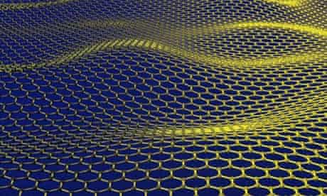
With graphene, everything from your fridge to your toothbrush could be hooked up to the internet. "How do you enable the Internet of Things? You need to put devices in everything. But you can't put a Pentium 5 processor in a book; it'll cost more than the book," "The Internet of Things will need very cheap, simple, flexible and eventually disposable devices, and that's where graphene comes in."
Decades on, the prospect of a vibrant market for personal body armour spun from spider silk probably overestimated the dangers of modern life as much as the practical hurdles that come with using the material.
"You can't use spider silk to make a bulletproof vest. It's too extensible. It would catch the bullet, but not before the bullet had passed through your body .
And yet scientists remain fascinated. That's because it's an exquisite material to learn from and will, Vollrath says, inspire researchers to make better materials in the future. Spider silk is made from a biopolymer called an aquamelt, which can be spun at room temperature 1,000 times more efficiently than plastics that need to be heated up and cooled down. By controlling the rate at which the silk is spun, a spider can control the stiffness or flexibility of the fibres. The goal for researchers is to make other materials that mimic spider silk's tricks .
Metamaterials
Metamaterials bingo remains – inexplicably – a niche hobby, but there is no doubting the genuine excitement around the materials. They owe their existence, in large part, to the enormously competitive microchip industry, which has refined manufacturing at the nano scale. Metamaterials are made with the same technology, but their design is so precise that scientists can control how electrons inside the materials respond when light – or other electromagnetic waves – strike them. This makes it possible to manipulate radiation like never before.
where much of the work on cloaking devices has been pioneered.
The materials themselves vary. To control radiowaves, you can use copper and fibreglass. To make metamaterials that bend infrared light, you can use semiconductors. Cloaking devices are still little more than party tricks, but that's changing. Objects can be hidden at some wavelengths and not others, or only under specific conditions, such as with polarised light, or from a particular angle. It's unlikely a cloak will ever make something completely vanish: even if an object is invisible to the naked eye, there's always radar and infrared imaging to turn to. "As a general rule, an object that's invisible at one wavelength will be visible at another. You can make a cloak work across a range of wavelengths, but not the whole electromagnetic spectrum,"
Materials conduct electricity when electrons flow through them. However, in most materials, the electrons are held up by impurities and other features that give rise to resistance. This resistance generates heat, and so electronics must be cooled to stop them melting. Stanene promises to change all that. The structure of the material allows electrons to shoot along channels with no resistance whatsoever. Add a little fluorine and, according to Zhang, the material will have zero resistance at more than 100C (212F).
Zhang sees stanene as the natural successor to copper interconnects in computers. This might seem niche, but atomically thin connections that don't heat up would enable designers to miniaturise electronics even more. Ultimately, Zhang says stanene could replace silicon as a cheap and abundant material from which to make computer chips.
1 .1 Historical Perspective
Understanding of how materials behave like they do, and why they differ in properties was only possible with the atomistic understanding allowed by quantum mechanics, that first explained atoms and then solids starting in the 1930s. The combination of physics, chemistry, and the focus on the relationship between the properties of a material and its microstructure is the domain of Materials Science. The development of this science allowed designing materials and provided a knowledge base for the engineering applications (Materials Engineering).
Structure:
Processing of materials is the application of heat (heat treatment), mechanical forces, etc. to affect their microstructure and, therefore, their properties.
1.4 Classification of Materials
Materials used in "High-Tec" applications, usually designed for maximum performance, and normally expensive. Examples are titanium alloys for supersonic airplanes, magnetic alloys for computer disks, special ceramics for the heat shield of the space shuttle, etc.
1.6 Modern Material's Needs
Atoms are composed of electrons, protons, and neutrons. Electron and protons are negative and positive charges of the same magnitude, 1.6 × 10⁻¹⁹ Coulombs.
The mass of the electron is negligible with respect to those of the proton and the neutron, which form the nucleus of the atom. The unit of mass is an atomic mass unit (amu) = 1.66 × 10⁻²⁷ kg, and equals 1/12 the mass of a carbon atom. The Carbon nucleus has Z=6, and A=6, where Z is the number of protons, and A the number of neutrons. Neutrons and protons have very similar masses, roughly equal to 1 amu. A neutral atom has the same number of electrons and protons, Z.
A mole is the amount of matter that has a mass in grams equal to the atomic mass in amu of the atoms. Thus, a mole of carbon has a mass of 12 grams. The number of atoms in a mole is called the Avogadro number, Nav = 6.023 × 10²³. Note that Nav = 1 gram/1 amu.
Calculating n, the number of atoms per cm3 in a piece of material of density d (g/cm3).
For a molecular solid like ice, one uses the molecular mass, M(H2O) = 18. With a density of 1 g/cm3, one obtains n = 3.3 × 10²² H2O/cm3. Note that since the water molecule contains 3 atoms, this is equivalent to 9.9 × 10²² atoms/cm3.
Most solids have atomic densities around 6 × 10²² atoms/cm3. The cube root of that number gives the number of atoms per centimeter, about 39 million. The mean distance between atoms is the inverse of that, or 0.25 nm. This is an important number that gives the scale of atomic structures in solids.
2.3 Electrons in Atoms
The forces in the atom are repulsions between electrons and attraction between electrons and protons. The neutrons play no significant role. Thus, Z is what characterizes the atom.
The electrons form a cloud around the neutron, of radius of 0.05 – 2 nanometers. Electrons do not move in circular orbits, as in popular drawings, but in 'fuzzy' orbits. We cannot tell how it moves, but only say what is the probability of finding it at some distance from the nucleus. According to quantum mechanics, only certain orbits are allowed (thus, the idea of a mini planetary system is not correct). The orbits are identified by a principal quantum number n, which can be related to the size, n = 0 is the smallest; n = 1, 2 .. are larger. (They are "quantized" or discrete, being specified by integers). The angular momentum l is quantized, and so is the projection in a specific direction m. The structure of the atom is determined by the Pauli exclusion principle, only two electrons can be placed in an orbit with a given n, l, m – one for each spin. Table 2.1 in the textbook gives the number of electrons in each shell (given by n) and subshells (given by l).
2.4 The Periodic Table
Elements are categorized by placing them in the periodic table. Elements in a column share similar properties. The noble gases have closed shells, and so they do not gain or lose electrons near another atom. Alkalis can easily lose an electron and become a closed shell; halogens can easily gain one to form a negative ion, again with a closed shell. The propensity to form closed shells occurs in molecules, when they share electrons to close a molecular shell. Examples are H2, N2, and NaCl.
The ability to gain or lose electrons is termed electronegativity or electropositivity, an important factor in ionic bonds.
2.5 Bonding Forces and Energies
The Coulomb forces are simple: attractive between electrons and nuclei, repulsive between electrons and between nuclei. The force between atoms is given by a sum of all the individual forces, and the fact that the electrons are located outside the atom and the nucleus in the center.
When two atoms come very close, the force between them is always repulsive, because the electrons stay outside and the nuclei repel each other. Unless both atoms are ions of the same charge (e.g., both negative) the forces between atoms is always attractive at large internuclear distances r. Since the force is repulsive at small r, and attractive at small r, there is a distance at which the force is zero. This is the equilibrium distance at which the atoms prefer to stay.
The interaction energy is the potential energy between the atoms. It is negative if the atoms are bound and positive if they can move away from each other. The interaction energy is the integral of the force over the separation distance, so these two quantities are directly related. The interaction energy is a minimum at the equilibrium position. This value of the energy is called the bond energy, and is the energy needed to separate completely to infinity (the work that needs to be done to overcome the attractive force.) The strongest the bond energy, the hardest is to move the atoms, for instance the hardest it is to melt the solid, or to evaporate its atoms.
2.6 Primary Interatomic Bonds
Ionic Bonding
This is the bond when one of the atoms is negative (has an extra electron) and another is positive (has lost an electron). Then there is a strong, direct Coulomb attraction. An example is NaCl. In the molecule, there are more electrons around Cl, forming Cl- and less around Na, forming Na+. Ionic bonds are the strongest bonds. In real solids, ionic bonding is usually combined with covalent bonding. In this case, the fractional ionic bonding is defined as %ionic = 100 × [1 – exp(-0.25 (XA – XB)2], where XA and XB are the electronegativities of the two atoms, A and B, forming the molecule.
Covalent Bonding
In covalent bonding, electrons are shared between the molecules, to saturate the valency. The simplest example is the H2 molecule, where the electrons spend more time in between the nuclei than outside, thus producing bonding.
Metallic Bonding
In metals, the atoms are ionized, loosing some electrons from the valence band. Those electrons form a electron sea, which binds the charged nuclei in place, in a similar way that the electrons in between the H atoms in the H2 molecule bind the protons.
2.7 Secondary Bonding (Van der Waals)
Fluctuating Induced Dipole Bonds
Since the electrons may be on one side of the atom or the other, a dipole is formed: the + nucleus at the center, and the electron outside. Since the electron moves, the dipole fluctuates. This fluctuation in atom A produces a fluctuating electric field that is felt by the electrons of an adjacent atom, B. Atom B then polarizes so that its outer electrons are on the side of the atom closest to the + side (or opposite to the – side) of the dipole in A. This bond is called van der Waals bonding.
Polar Molecule-Induced Dipole Bonds
A polar molecule like H2O (Hs are partially +, O is partially – ), will induce a dipole in a nearby atom, leading to bonding.
Permanent Dipole Bonds
This is the case of the hydrogen bond in ice. The H end of the molecule is positively charged and can bond to the negative side of another dipolar molecule, like the O side of the H2O dipole.
2.8 Molecules
If molecules formed a closed shell due to covalent bonding (like H2, N2) then the interaction between molecules is weak, of the van der Waals type. Thus, molecular solids usually have very low melting points.
Atomic mass unit (amu)
Atomic number
Atomic weight
Bonding energy
Coulombic force
Covalent bond
Dipole (electric)
Electron state
Electronegative
Electropositive
Hydrogen bond
Ionic bond
Metallic bond
Mole
Molecule
Periodic table
Polar molecule
Primary bonding
Secondary bonding
Valence electron
To discuss crystalline structures it is useful to consider atoms as being hard spheres, with well-defined radii. In this scheme, the shortest distance between two like atoms is one diameter.
3.4 Metallic Crystal Structures
Important properties of the unit cells are
The closest packed direction in a BCC cell is along the diagonal of the cube; in a FCC cell is along the diagonal of a face of the cube.

3.7 – 3.10 Crystallography – Not Covered
Terms:
An interstitial is an atom that occupies a place outside the normal lattice position. It may be the same type of atom as the others (self interstitial) or an impurity atom.
In the case of vacancies and interstitials, there is a change in the coordination of atoms around the defect. This means that the forces are not balanced in the same way as for other atoms in the solid, which results in lattice distortion around the defect.
The number of vacancies formed by thermal agitation follows the law:
When QV is given in joules, k = 1.38 × 10⁻²³ J/atom-K. When using eV as the unit of energy, k = 8.62 × 10⁻⁵ eV/atom-K.
Note that kT(300 K) = 0.025 eV (room temperature) is much smaller than typical vacancy formation energies. For instance, QV(Cu) = 0.9 eV/atom. This means that NV/NA at room temperature is exp(-36) = 2.3 × 10⁻¹⁶, an insignificant number. Thus, a high temperature is needed to have a high thermal concentration of vacancies. Even so, NV/NA is typically only about 0.0001 at the melting point.
Impurities are often added to materials to improve the properties. For instance, carbon added in small amounts to iron makes steel, which is stronger than iron. Boron impurities added to silicon drastically change its electrical properties.
Solid solutions are made of a host, the solvent or matrix) which dissolves the solute (minor component). The ability to dissolve is called solubility. Solid solutions are:
Edge dislocations occur when an extra plane is inserted. The dislocation line is at the end of the plane. In an edge dislocation, the Burgers vector is perpendicular to the dislocation line.
Screw dislocations result when displacing planes relative to each other through shear. In this case, the Burgers vector is parallel to the dislocation line.
Surfaces and interfaces are very reactive and it is usual that impurities segregate there. Since energy is required to form a surface, grains tend to grow in size at the expense of smaller grains to minimize energy. This occurs by diffusion, which is accelerated at high temperatures.
Twin boundaries: not covered
The description of stress-strain behavior is similar to that of metals, but a very important consideration for polymers is that the mechanical properties depend on the strain rate, temperature, and environmental conditions.
The stress-strain behavior can be brittle, plastic and highly elastic (elastomeric or rubber-like), see Fig. 16. 1. Tensile modulus (modulus) and tensile strengths are orders of magnitude smaller than those of metals, but elongation can be up to 1000 % in some cases. The tensile strength is defined at the fracture point (Fig. 16.2) and can be lower than the yield strength.
Mechanical properties change dramatically with temperature, going from glass-like brittle behavior at low temperatures (like in the liquid-nitrogen demonstration) to a rubber-like behavior at high temperatures (Fig. 16.3).
In general, decreasing the strain rate has the same influence on the strain-strength characteristics as increasing the temperature: the material becomes softer and more ductile.
Deformation of Semicrystalline Polymers
Many semicrystalline polymers have the spherulitic structure and deform in the following steps (Fig. 16.4):
Factors that Influence the Mechanical Properties of Polymers
The tensile modulus decreases with increasing temperature or diminishing strain rate.
Obstacles to the steps mentioned in 16.4 strengthen the polymer. Examples are cross-linking (aligned chains have more van der Waals inter-chain bonds) and a large mass (longer molecules have more inter-chain bonds). Crystallinity increases strength as the secondary bonding is enhanced when the molecular chains are closely packed and parallel. Pre-deformation by drawing, analogous to strain hardening in metals, increases strength by orienting the molecular chains. For undrawn polymers, heating increases the tensile modulus and yield strength, and reduces the ductility - opposite of what happens in metals.
Crystallization, Melting, and Glass Transition Phenomena
Crystallization rates are governed by the same type of S-curves we saw in the case of metals (Fig. 16.7). Nucleation becomes slower at higher temperatures.
The melting behavior of semicrystalline polymers is intermediate between that of crystalline materials (sharp density change at a melting temperature) and that of a pure amorphous material (slight change in slope of density at the glass-transition temperature). The glass transition temperature is between 0.5 and 0.8 of the melting temperature.
The melting temperature increases with the rate of heating, thickness of the lamellae, and depends on the temperature at which the polymer was crystallized.
Melting involves breaking of the inter-chain bonds, so the glass and melting temperatures depend on:
Thermoplastic and Thermosetting Polymers
Thermoplastic polymers (thermoplasts) soften reversibly when heated (harden when cooled back)
Thermosetting polymers (thermosets) harden permanently when heated, as cross-linking hinder bending and rotations. Thermosets are harder, more dimensionally stable, and more brittle than thermoplasts.
Viscoelasticity
At low temperatures, amorphous polymers deform elastically, like glass, at small elongation. At high temperatures the behavior is viscous, like liquids. At intermediate temperatures, the behavior, like a rubbery solid, is termed viscoelastic.
Viscoelasticity is characterized by the viscoelastic relaxation modulus
Er = s(t)/e0.
If the material is strained to a value e0.it is found that the stress needs to be reduced with time to maintain this constant value of strain (see figs. 16.11 and 16.12).
In viscoelastic creep, the stress is kept constant at s0 and the change of deformation with time e(t) is measured. The time-dependent creep modulus is given by
Ec = s0/e(t).
Deformation and Elastomers
Elastomers can be deformed to very large strains and the spring back elastically to the original length, a behavior first observed in natural rubber. Elastic elongation is due to uncoiling, untwisting and straightening of chains in the stress direction.
To be elastomeric, the polymer needs to meet several criteria:
As other mechanical properties, the fracture strength of polymers is much lower than that of metals. Fracture also starts with cracks at flaws, scratches, etc. Fracture involves breaking of covalent bonds in the chains. Thermoplasts can have both brittle and ductile fracture behaviors. Glassy thermosets have brittle fracture at low temperatures and ductile fracture at high temperatures.
Glassy thremoplasts often suffer grazing before brittle fracture. Crazes are associated with regions of highly localized yielding which leads to the formation of interconnected microvoids (Fig. 16.15). Crazing absorbs energy thus increasing the fracture strength of the polymer.
Miscellaneous Characteristics
Polymers are brittle at low temperatures and have low impact strengths (Izod or Charpy tests), and a brittle to ductile transition over a narrow temperature range.
Fatigue is similar to the case of metals but at reduced loads and is more sensitive to frequency due to heating which leads to softening.
Polymerization
Polymerization is the synthesis of high polymers from raw materials like oil or coal. It may occur by:
Elastomers
In vulcanization, crosslinking of the elastomeric polymer is achieved by an irreversible chemical reaction usually at high temperatures (hence ‘vulcan’), and usually involving the addition of sulfur compounds. The S atoms are the ones that form the bridge cross-links. Elastomers are thermosetting due to the cross-linking.
Rubbers become harder and extend less with increasing sulfur content. For automobile applications, synthetic rubbers are strengthened by adding carbon black.
In silicone rubbers, the backbone C atoms are replaced by a chain of alternating silicon and oxygen atoms. These elastomers are also cross-linked and are stable to higher temperatures than C-based elastomers.
New - High-tech materials, engineered to specific applications
Old - brick-straw composites, paper, known for > 5000 years.
A type of composite that has been discussed is perlitic steel, which combines hard, brittle cementite with soft, ductile ferrite to get a superior material.
Natural composites: wood (polymer-polymer), bones (polymer-ceramics).
Usual composites have just two phases:
Properties are a combination of those of the components. The rule of mixtures predicts that an upper limit of the elastic modulus of the composite is given in terms of the elastic moduli of the matrix (Em) and the particulate (Ep) phases by:
Ec = EmVm + EpVp
where Vm and Vp are the volume fraction of the two phases. A lower bound is given by:
Ec = EmEp / (EpVm + EmVp)
Fig. 17.3 - modulus of composite of WC particles in Cu matrix vs. WC concentration.Concrete The most common large-particle composite is concrete, made of a cement matrix that bonds particles of different size (gravel and sand.) Cement was already known to the Egyptians and the Greek. Romans made cement by mixing lime (CaO) with volcanic ice.
In its general from, cement is a fine mixture of lime, alumina, silica, and water. Portland cement is a fine powder of chalk, clay and lime-bearing minerals fired to 1500o C (calcinated). It forms a paste when dissolved in water. It sets into a solid in minutes and hardens slowly (takes 4 months for full strength). Properties depend on how well it is mixed, and the amount of water: too little - incomplete bonding, too much - excessive porosity.
The advantage of cement is that it can be poured in place, it hardens at room temperature and even under water, and it is very cheap. The disadvantages are that it is weak and brittle, and that water in the pores can produce crack when it freezes in cold weather.
Concrete is cement strengthened by adding particulates. The use of different size (stone and sand) allows better packing factor than when using particles of similar size.
Concrete is improved by making the pores smaller (using finer powder, adding polymeric lubricants, and applying pressure during hardening.
Reinforced concrete is obtained by adding steel rods, wires, mesh. Steel has the advantage of a similar thermal expansion coefficient, so there is reduced danger of cracking due to thermal stresses. Pre-stressed concrete is obtained by applying tensile stress to the steel rods while the cement is setting and hardening. When the tensile stress is removed, the concrete is left under compressive stress, enabling it to sustain tensile loads without fracturing. Pre-stressed concrete shapes are usually prefabricated. A common use is in railroad or highway bridges.Cermets are composites of ceramic particles (strong, brittle) in a metal matrix (soft, ductile) that enhances toughness. For instance, tungsten carbide or titanium carbide ceramics in Co or Ni. They are used for cutting tools for hardened steels. Reinforced rubber is obtained by strengthening with 20-50 nm carbon-black particles. Used in auto tires.
Dispersion-Strengthened Composites
Use of very hard, small particles to strengthen metals and metal alloys. The effect is like precipitation hardening but not so strong. Particles like oxides do not react so the strengthening action is retained at high temperatures.
The strength depends on the fiber length and its orientation with respect to the stress direction.
The efficiency of load transfer between matrix and fiber depends on the interfacial bond.
Influence of Fiber Length
Normally the matrix has a much lower modulus than the fiber so it strains more. This occurs at a distance from the fiber. Right next to the fiber, the strain is limited by the fiber. Thus, for a composite under tension, a shear stress appears in the matrix that pulls from the fiber. The pull is uniform over the area of the fiber. This makes the force on the fiber be minimum at the ends and maximum in the middle, like in the tug-of-war game.
To achieve effective strengthening and stiffening, the fibers must be larger than a critical length lc, defined as the minimum length at which the center of the fiber reaches the ultimate (tensile) strength sf, when the matrix achieves the maximum shear strength tm:
lc = sf d /2 tm
Since it is proportional to the diameter of the fiber d, a more unified condition for effective strengthening is that the aspect ratio of the fiber is l/d > sf /2 tm.
Influence of Fiber Orientation
The composite is stronger along the direction of orientation of the fibers and weakest in a direction perpendicular to the fiber. For discontinuous, random fibers, the properties are isotropic.
Polymer Matrix Composites
Largest and most diverse use of composites due to ease of fabrication, low cost and good properties.
Glass-fiber reinforced composites (GFRC) are strong, corrosion resistant and lightweight, but not very stiff and cannot be used at high temperatures. Applications include auto and boat bodies, aircraft components.
Carbon-fiber reinforced composites (CFRC) use carbon fibers, which have the highest specific module (module divided by weight). CFRC are strong, inert, allow high temperature use. Applications include fishing rods, golf clubs, aircraft components.
Kevlar, and aremid-fiber composite (Fig. 17.9) can be used as textile fibers. Applications include bullet-proof vests, tires, brake and clutch linings.Wood This is one of the oldest and the most widely used structural material. It is a composite of strong and flexible cellulose fibers (linear polymer) surrounded and held together by a matrix of lignin and other polymers. The properties are anisotropic and vary widely among types of wood. Wood is ten times stronger in the axial direction than in the radial or tangential directions.
Laminar Composites
Sheets (panels) with different orientation of high strength directions are stacked and glued together, producing a material with more isotropic strength in the plane. Examples are plywood and modern skis.
Sandwich Panels
Strong, stiff end sheets are bonded to lightweight core structure, for instance honeycomb (Fig. 17.16) which provides strength to shear. It is used in roofs, walls, and aircraft structures.
Terms:

“Heat flow occurs whenever you have a region of higher temperature near a region of lower temperature,” said William King, the Ralph A. Andersen Endowed Chair and Professor in the Department of Mechanical Science and Engineering and the project co-leader. “In order to control the heat flow, we engineered a specific heat flow path between the hot region and cold region, and then created a way to break the heat flow path when desired.”
“The technology is based on the motion of a liquid metal droplet .
Modern society is heavily dependent on advanced materials: lightweight composites for faster vehicles, optical fibres for telecommunications and silicon microchips for the information revolution. Materials scientists study the relationships between the structure and properties of a material and how it is made. They also develop new materials and devise processes for manufacturing them. Materials Science is vital for developments in nanotechnology, quantum computing and nuclear fusion, as well as medical technologies such as bone replacement materials.
This diverse programme spans the subject from its foundations in physics and chemistry to the mechanical, electrical, magnetic and optical properties of materials, and the design, manufacture and applications of metals, alloys, ceramics, polymers, composites and biomaterials. This work is supported by excellent laboratory and teaching facilities.

"Industrial processes making use of less harmful visible light are scarce -- a sharp contrast to what occurs in nature.
"For plants, visible light plays a critical role in chemical processes. Trees harvest light during the day and use this as an energy source to grow, releasing oxygen in the process. At night, however, when light is no longer available, the chemical process is altered and plants release carbon dioxide.
"We've been inspired by such natural processes and designed a completely light-switchable chemical reaction system for the first time."
The research team said their system may be applied to create light-sensitive materials for 3D laser lithography, allowing printing of very small structures that could be used in such things as computer chip fabrication. 3D laser lithography is a type of 3D printing with direct laser light, and used for creating very precise structures in the micro range, such as scaffolds for cells.
"Contemporary chip fabrication is a complex, and expensive, system of chemical processes," "Here, due to the so-called light diffraction limit, radiation with short wavelengths -- which is very harsh UV light -- is used.
"But what if we could use visible light to reversibly switch certain chemical processes and get around the light diffraction limit and print very, very small structures, for example five nanometres wide?
"Being able to switch chemical reactivity within 3D laser lithography could revolutionise chip printing, and make it cheaper, simpler and safer.
"There are substantial barriers to overcome, but potentially the system we have devised with visible light as a chemical deactivation mechanism could provide an avenue to achieve that."

- Every element has got a distinct atomic diameter that is different from other elements. When a solid solution is formed the solute atoms will be either largest or small in diameter when compared to the solvent atoms.
- Since solvent and solute atoms have different sizes when solute is added to solvent, distortion of lattices takes place. Based on size of solute there are two types of solid solutions. They are interstitial solid solutions and substitutional solid solutions.
- In interstitial solid solutions the solute is smaller in size when compared to solvent atoms and this solute occupies a space in between the solvent atoms. In this case tensile fields areas set up. E.g.. Carbon, Hydrogen, Nitrogen and Iron.
- In solid solutions of substitutional type the solute atoms is approximately the same size as that of the solvent atoms and this solute occupies a space in between the solvent atoms and in this case compressive fields are set up.
- The more the different between atomic size of solute and solvent the higher is the stress field around solute atoms thereby providing more resistance to the motion of dislocation and thereby increasing the tensile strength.
- If the number of solute atoms is more greater will be the local distortion in the lattice and hence more will the resistance to moving dislocation and there by increasing the hardness and strength of the material.
Dispersion Hardening:
This means a strengthening a metal by creating a fine dispersion of insoluble particles o a second phase within the metal. The insoluble particles may be slag inclusions, inter metallic compound formed between the alloying elements and any other impurity atoms. The presence of finely distributed hard particles obstruct the flow pattern of the stress deformation and causes rapid hardening. The effect depends upon the size, shape, concentration and physical characteristics.
Age hardening:
This is the phenomenon observed in many non-ferrous alloys like Al, Si, Mg alloys whereby the hardness of the material increase with time. The essential requirement for precipitation to occur in solution is the decreasing solubility of a solute with decreasing temperatures. This results in super saturated solid solution that being unstable tends to decompose according to the relation.
Super saturated a solid solution = saturated solution a + b precipitation.
Age hardening involves the following mentioned stages
Heating: The alloy is first solutionized by heating into a single phase reaction, held there long enough to dissolve all existing soluble precipitate particles.
Quenching: After solutionizing, the alloy is rapidly quenched into the two phase reaction region. The rapidity of the quench prevents the formation of equilibrium precipitates and thus produces the supersaturated solid solution. The quenching medium is usually water.
Aging: On aging at or above room temperature, fine scale transition structures as small as 100 Angstrom is formed.
Strain hardening:
In most of the metals and alloys it is observed that the yield strength of the material increases after the material undergoes plastic deformation from the stress-strain curve shown. Strain hardening or work hardening is the phenomenon which results in an increase in hardness and strength of a metal subjected to plastic deformation at temperatures lower than the re-crystallisation range. Strain hardening however reduces ductility and plasticity.
An important characteristic of plastic deformation of metals is that the shear stress required to produce slip continuously increases with shear strain. When the metal is loaded, the strain increases with stress and the curve reaches a point A in the plastic region. If at this stage, the specimen is unloaded, the strain does not recover along the original part AO, but moves along AB. If the specimen is reloaded immediately the curve again rises from B to A, and reaches the point C, after which it still follows the curvature, if loading is continued. IF the specimen would not have been unloaded, after point A, the stress-strain curve would have followed the dotted path AD'.
The figure shows the stress strain curve of FCC crystal. There are three regions of hardening and are experimentally distinguishable. The forest dislocation theory stages that when a material is stressed the dislocation starts moving which results in plastic deformation. Even as the stress increase the number of dislocations present in the body increase exponentially by frank reed source mechanism. The movement of a large number of dislocation along different slip lanes creates a traffic jam like situation and there by making it difficult for any movement of dislocation. Therefore further plastic deformation requires more stress or more load.
Stage I or the easy glide region, immediately follows the yield point and is characterized by little strain hardening undergone by the crystal. During easy glide the dislocation are able to move over relatively large distances without encountering barriers.
Stage II region marks a rapid increase in work hardening, the slope of which is approximately independent of applied stress, temperature, orientation alloy content. In this region slip occurs on both primary and secondary slip systems. As a result, several new lattice irregularities may be formed which will include.
- Forest dislocations
- Lomer - cottrell barriers,
- Jogs produced either by moving dislocations cutting through forest dislocations or by forest locations cutting through source dislocations
There are three theories that explain the hardening mechanism at this stage. They are pile-up theory, forest theory and jog theory. The pile up theory states that some of the dislocations give out by the frank reed sources are eventually stopped at barriers, according to this theory, the hardening is principally due to long range internal stresses from piled up groups interacting with guide dislocations.
Stage III is the region of decreasing rate of strain hardening. At the sufficiently high stress value or temperature in region 3, the dislocations help up in stage 2 are able to move by a process that had been suppressed at lower stresses and temperatures. In this mechanism, dislocations can by-pass the obstacles in their guide plane and do not have to interact strongly with them. For this reason, this stage exhibits a lower rate of work hardening.
Grain boundary hardening:
It is a relevant fact that the dislocations are obstructed by the grain boundaries during plastic deformation of the material. This is basically due to the disordered at grain boundaries, that is in the grain boundary the atoms are not arranged in any particular fashion by arranged randomly. It requires large amount of force for the dislocations to travel through the disordered structure, than along the slip planes. Transmission electron microscope picture have revealed that dislocations get piled up like grain boundary as the deformation process at this stage the stress concentration near the grain boundary must be sufficient to nucleate slip in the next grain. In a material with fine grains the area of grain boundary within gives a volume that is going to be very high compared to materials with large grains. So the materials with fine grain will have higher strain. This effect is called grain boundary strengthening or hardening.
XXX . XXX Five wonder materials that could change the world
Materials such as graphene and shrilk are so new that the scientists who discovered them hardly know what to do with them – they only know they might yet transform our lives
Graphene
The Friday evening antics that led to the invention of graphene have become the stuff of scientific legend , were playing around with Scotch tape and a lump of graphite when they found they could make sheets of carbon one atom thick . And all for good reason. Graphene is an extraordinary material. Apart from its many other properties, it's immensely strong, flexible, transparent and conductive. This makes it perfect for the next generation of electronic devices, the sort that might be sewn into our clothing, slapped on drinks bottles and cans of food or rolled up and tucked in our pockets. graphene might be used to make night-vision contact lenses."Graphene has huge potential,"
With graphene, everything from your fridge to your toothbrush could be hooked up to the internet. "How do you enable the Internet of Things? You need to put devices in everything. But you can't put a Pentium 5 processor in a book; it'll cost more than the book," "The Internet of Things will need very cheap, simple, flexible and eventually disposable devices, and that's where graphene comes in."
Spider silk
Long, long ago, in the history of science, there was a time when researchers didn't speak of spider silk as the perfect material from which to manufacture bulletproof vests. The application was touted around after researchers teased out the silk's molecular structure and from that came to understand its fantastic strength and flexibility.Decades on, the prospect of a vibrant market for personal body armour spun from spider silk probably overestimated the dangers of modern life as much as the practical hurdles that come with using the material.
"You can't use spider silk to make a bulletproof vest. It's too extensible. It would catch the bullet, but not before the bullet had passed through your body .
And yet scientists remain fascinated. That's because it's an exquisite material to learn from and will, Vollrath says, inspire researchers to make better materials in the future. Spider silk is made from a biopolymer called an aquamelt, which can be spun at room temperature 1,000 times more efficiently than plastics that need to be heated up and cooled down. By controlling the rate at which the silk is spun, a spider can control the stiffness or flexibility of the fibres. The goal for researchers is to make other materials that mimic spider silk's tricks .
Metamaterials
Metamaterials bingo remains – inexplicably – a niche hobby, but there is no doubting the genuine excitement around the materials. They owe their existence, in large part, to the enormously competitive microchip industry, which has refined manufacturing at the nano scale. Metamaterials are made with the same technology, but their design is so precise that scientists can control how electrons inside the materials respond when light – or other electromagnetic waves – strike them. This makes it possible to manipulate radiation like never before.
where much of the work on cloaking devices has been pioneered.
The materials themselves vary. To control radiowaves, you can use copper and fibreglass. To make metamaterials that bend infrared light, you can use semiconductors. Cloaking devices are still little more than party tricks, but that's changing. Objects can be hidden at some wavelengths and not others, or only under specific conditions, such as with polarised light, or from a particular angle. It's unlikely a cloak will ever make something completely vanish: even if an object is invisible to the naked eye, there's always radar and infrared imaging to turn to. "As a general rule, an object that's invisible at one wavelength will be visible at another. You can make a cloak work across a range of wavelengths, but not the whole electromagnetic spectrum,"
Shrilk
What to call a material made from leftover shrimp shells and proteins derived from silk
Shrilk was inspired by research into the tough skins of insects. The coating is made from layers of a material called chitin and a protein called fibroin. In one arrangement, the material is strong and rigid enough to form the insect's protective exoskeleton. What intrigued the Harvard group was that simple tweaks to the material – specifically the amount of water bound inside it – changed its behaviour dramatically. Without water the material is stiff, but with water the coating becomes very flexible.
fibroin from silk worms and chitosan, a material similar to chitin, to make their first batch of shrilk. They then played with the water bound inside the material to vary its properties. They can form strong, transparent sheets of shrilk that are biodegradable and even enrich the soil like a fertiliser as it breaks down. Bob Cunningham, also at the Wyss Institute, says shrilk is an environmentally friendly alternative to plastics. "It might not make sense to make the trash bin that you're going to use for 10 years out of this material, but a trash bag you might fill up in a day or a week that goes to landfill? That makes a lot more sense," says Cunningham. The components are FDA-approved for use in the body, where they could find a role as sutures, or scaffolds for growing new tissues that dissolve when they are no longer needed.
Stanene
Stanene was created – virtually, that is – by Shoucheng Zhang at Stanford University. Scientists call it a topological insulator, but the name isn't wildly helpful. Stanene is an insulator on the inside, and a conductor on the outside. Thin layers of stanene – or one-atom-thick sheets of tin – are essentially all surface, and should conduct electricity with 100% efficiency.Materials conduct electricity when electrons flow through them. However, in most materials, the electrons are held up by impurities and other features that give rise to resistance. This resistance generates heat, and so electronics must be cooled to stop them melting. Stanene promises to change all that. The structure of the material allows electrons to shoot along channels with no resistance whatsoever. Add a little fluorine and, according to Zhang, the material will have zero resistance at more than 100C (212F).
Zhang sees stanene as the natural successor to copper interconnects in computers. This might seem niche, but atomically thin connections that don't heat up would enable designers to miniaturise electronics even more. Ultimately, Zhang says stanene could replace silicon as a cheap and abundant material from which to make computer chips.
XXX . XXX Material science for Electronic and Machine Engineering
Introduction
Materials are so important in the development of civilization that we associate Ages with them. In the origin of human life on Earth, the Stone Age, people used only natural materials, like stone, clay, skins, and wood. When people found copper and how to make it harder by alloying, the Bronze Age started about 3000 BC. The use of iron and steel, a stronger material that gave advantage in wars started at about 1200 BC. The next big step was the discovery of a cheap process to make steel around 1850, which enabled the railroads and the building of the modern infrastructure of the industrial world.
1.2 Materials Science and Engineering Understanding of how materials behave like they do, and why they differ in properties was only possible with the atomistic understanding allowed by quantum mechanics, that first explained atoms and then solids starting in the 1930s. The combination of physics, chemistry, and the focus on the relationship between the properties of a material and its microstructure is the domain of Materials Science. The development of this science allowed designing materials and provided a knowledge base for the engineering applications (Materials Engineering).
Structure:
- At the atomic level: arrangement of atoms in different ways. (Gives different properties for graphite than diamond both forms of carbon.)
- At the microscopic level: arrangement of small grains of material that can be identified by microscopy. (Gives different optical properties to transparent vs. frosted glass.)
Processing of materials is the application of heat (heat treatment), mechanical forces, etc. to affect their microstructure and, therefore, their properties.
1.3 Why Study Materials Science and Engineering?
- To be able to select a material for a given use based on considerations of cost and performance.
- To understand the limits of materials and the change of their properties with use.
- To be able to create a new material that will have some desirable properties.
1.4 Classification of Materials
Like many other things, materials are classified in groups, so that our brain can handle the complexity. One could classify them according to structure, or properties, or use. The one that we will use is according to the way the atoms are bound together:
Metals: valence electrons are detached from atoms, and spread in an 'electron sea' that "glues" the ions together. Metals are usually strong, conduct electricity and heat well and are opaque to light (shiny if polished). Examples: aluminum, steel, brass, gold.
Semiconductors: the bonding is covalent (electrons are shared between atoms). Their electrical properties depend extremely strongly on minute proportions of contaminants. They are opaque to visible light but transparent to the infrared. Examples: Si, Ge, GaAs.
Ceramics: atoms behave mostly like either positive or negative ions, and are bound by Coulomb forces between them. They are usually combinations of metals or semiconductors with oxygen, nitrogen or carbon (oxides, nitrides, and carbides). Examples: glass, porcelain, many minerals.
Polymers: are bound by covalent forces and also by weak van der Waals forces, and usually based on H, C and other non-metallic elements. They decompose at moderate temperatures (100 – 400 C), and are lightweight. Other properties vary greatly. Examples: plastics (nylon, Teflon, polyester) and rubber.
Other categories are not based on bonding. A particular microstructure identifies composites, made of different materials in intimate contact (example: fiberglass, concrete, wood) to achieve specific properties. Biomaterials can be any type of material that is biocompatible and used, for instance, to replace human body parts.
1.5 Advanced Materials1.6 Modern Material's Needs
- Engine efficiency increases at high temperatures: requires high temperature structural materials
- Use of nuclear energy requires solving problem with residues, or advances in nuclear waste processing.
- Hypersonic flight requires materials that are light, strong and resist high temperatures.
- Optical communications require optical fibers that absorb light negligibly.
- Civil construction – materials for unbreakable windows.
- Structures: materials that are strong like metals and resist corrosion like plastics.
Atoms are composed of electrons, protons, and neutrons. Electron and protons are negative and positive charges of the same magnitude, 1.6 × 10⁻¹⁹ Coulombs.
The mass of the electron is negligible with respect to those of the proton and the neutron, which form the nucleus of the atom. The unit of mass is an atomic mass unit (amu) = 1.66 × 10⁻²⁷ kg, and equals 1/12 the mass of a carbon atom. The Carbon nucleus has Z=6, and A=6, where Z is the number of protons, and A the number of neutrons. Neutrons and protons have very similar masses, roughly equal to 1 amu. A neutral atom has the same number of electrons and protons, Z.
A mole is the amount of matter that has a mass in grams equal to the atomic mass in amu of the atoms. Thus, a mole of carbon has a mass of 12 grams. The number of atoms in a mole is called the Avogadro number, Nav = 6.023 × 10²³. Note that Nav = 1 gram/1 amu.
Calculating n, the number of atoms per cm3 in a piece of material of density d (g/cm3).
n = Nav × d / M
where M is the atomic mass in amu (grams per mol). Thus, for graphite (carbon) with a density d = 1.8 g/cm3, M =12, we get 6 × 10²³ atoms/mol × 1.8 g/cm3 / 12 g/mol) = 9 × 10²² C/cm3. For a molecular solid like ice, one uses the molecular mass, M(H2O) = 18. With a density of 1 g/cm3, one obtains n = 3.3 × 10²² H2O/cm3. Note that since the water molecule contains 3 atoms, this is equivalent to 9.9 × 10²² atoms/cm3.
Most solids have atomic densities around 6 × 10²² atoms/cm3. The cube root of that number gives the number of atoms per centimeter, about 39 million. The mean distance between atoms is the inverse of that, or 0.25 nm. This is an important number that gives the scale of atomic structures in solids.
2.3 Electrons in Atoms
The forces in the atom are repulsions between electrons and attraction between electrons and protons. The neutrons play no significant role. Thus, Z is what characterizes the atom.
The electrons form a cloud around the neutron, of radius of 0.05 – 2 nanometers. Electrons do not move in circular orbits, as in popular drawings, but in 'fuzzy' orbits. We cannot tell how it moves, but only say what is the probability of finding it at some distance from the nucleus. According to quantum mechanics, only certain orbits are allowed (thus, the idea of a mini planetary system is not correct). The orbits are identified by a principal quantum number n, which can be related to the size, n = 0 is the smallest; n = 1, 2 .. are larger. (They are "quantized" or discrete, being specified by integers). The angular momentum l is quantized, and so is the projection in a specific direction m. The structure of the atom is determined by the Pauli exclusion principle, only two electrons can be placed in an orbit with a given n, l, m – one for each spin. Table 2.1 in the textbook gives the number of electrons in each shell (given by n) and subshells (given by l).
2.4 The Periodic Table
Elements are categorized by placing them in the periodic table. Elements in a column share similar properties. The noble gases have closed shells, and so they do not gain or lose electrons near another atom. Alkalis can easily lose an electron and become a closed shell; halogens can easily gain one to form a negative ion, again with a closed shell. The propensity to form closed shells occurs in molecules, when they share electrons to close a molecular shell. Examples are H2, N2, and NaCl.
The ability to gain or lose electrons is termed electronegativity or electropositivity, an important factor in ionic bonds.
2.5 Bonding Forces and Energies
The Coulomb forces are simple: attractive between electrons and nuclei, repulsive between electrons and between nuclei. The force between atoms is given by a sum of all the individual forces, and the fact that the electrons are located outside the atom and the nucleus in the center.
When two atoms come very close, the force between them is always repulsive, because the electrons stay outside and the nuclei repel each other. Unless both atoms are ions of the same charge (e.g., both negative) the forces between atoms is always attractive at large internuclear distances r. Since the force is repulsive at small r, and attractive at small r, there is a distance at which the force is zero. This is the equilibrium distance at which the atoms prefer to stay.
The interaction energy is the potential energy between the atoms. It is negative if the atoms are bound and positive if they can move away from each other. The interaction energy is the integral of the force over the separation distance, so these two quantities are directly related. The interaction energy is a minimum at the equilibrium position. This value of the energy is called the bond energy, and is the energy needed to separate completely to infinity (the work that needs to be done to overcome the attractive force.) The strongest the bond energy, the hardest is to move the atoms, for instance the hardest it is to melt the solid, or to evaporate its atoms.
2.6 Primary Interatomic Bonds
This is the bond when one of the atoms is negative (has an extra electron) and another is positive (has lost an electron). Then there is a strong, direct Coulomb attraction. An example is NaCl. In the molecule, there are more electrons around Cl, forming Cl- and less around Na, forming Na+. Ionic bonds are the strongest bonds. In real solids, ionic bonding is usually combined with covalent bonding. In this case, the fractional ionic bonding is defined as %ionic = 100 × [1 – exp(-0.25 (XA – XB)2], where XA and XB are the electronegativities of the two atoms, A and B, forming the molecule.
Covalent Bonding
In covalent bonding, electrons are shared between the molecules, to saturate the valency. The simplest example is the H2 molecule, where the electrons spend more time in between the nuclei than outside, thus producing bonding.
Metallic Bonding
In metals, the atoms are ionized, loosing some electrons from the valence band. Those electrons form a electron sea, which binds the charged nuclei in place, in a similar way that the electrons in between the H atoms in the H2 molecule bind the protons.
2.7 Secondary Bonding (Van der Waals)
Since the electrons may be on one side of the atom or the other, a dipole is formed: the + nucleus at the center, and the electron outside. Since the electron moves, the dipole fluctuates. This fluctuation in atom A produces a fluctuating electric field that is felt by the electrons of an adjacent atom, B. Atom B then polarizes so that its outer electrons are on the side of the atom closest to the + side (or opposite to the – side) of the dipole in A. This bond is called van der Waals bonding.
Polar Molecule-Induced Dipole Bonds
A polar molecule like H2O (Hs are partially +, O is partially – ), will induce a dipole in a nearby atom, leading to bonding.
Permanent Dipole Bonds
This is the case of the hydrogen bond in ice. The H end of the molecule is positively charged and can bond to the negative side of another dipolar molecule, like the O side of the H2O dipole.
2.8 Molecules
If molecules formed a closed shell due to covalent bonding (like H2, N2) then the interaction between molecules is weak, of the van der Waals type. Thus, molecular solids usually have very low melting points.
Terms:
Crystal Structures
3.2 Fundamental Concepts
Atoms self-organize in crystals, most of the time. The crystalline lattice, is a periodic array of the atoms. When the solid is not crystalline, it is called amorphous. Examples of crystalline solids are metals, diamond and other precious stones, ice, graphite. Examples of amorphous solids are glass, amorphous carbon (a-C), amorphous Si, most plasticsTo discuss crystalline structures it is useful to consider atoms as being hard spheres, with well-defined radii. In this scheme, the shortest distance between two like atoms is one diameter.
3.3 Unit Cells
The unit cell is the smallest structure that repeats itself by translation through the crystal. We construct these symmetrical units with the hard spheres. The most common types of unit cells are the faced-centered cubic (FCC), the body-centered cubic (FCC) and the hexagonal close-packed (HCP). Other types exist, particularly among minerals. The simple cube (SC) is often used for didactical purpose, no material has this structure.3.4 Metallic Crystal Structures
Important properties of the unit cells are
- The type of atoms and their radii R.
- cell dimensions (side a in cubic cells, side of base a and height c in HCP) in terms of R.
- n, number of atoms per unit cell. For an atom that is shared with m adjacent unit cells, we only count a fraction of the atom, 1/m.
- CN, the coordination number, which is the number of closest neighbors to which an atom is bonded.
- APF, the atomic packing factor, which is the fraction of the volume of the cell actually occupied by the hard spheres. APF = Sum of atomic volumes/Volume of cell.
| Unit Cell |
n
|
CN
|
a/R
|
APF
|
| SC |
1
|
6
|
2
|
0.52
|
| BCC |
2
|
8
|
4Ö 3
|
0.68
|
| FCC |
4
|
12
|
2Ö 2
|
0.74
|
| HCP |
6
|
12
|
0.74
|
3.5 Density Computations
The density of a solid is that of the unit cell, obtained by dividing the mass of the atoms (n atoms x Matom) and dividing by Vc the volume of the cell (a3 in the case of a cube). If the mass of the atom is given in amu (A), then we have to divide it by the Avogadro number to get Matom. Thus, the formula for the density is:3.6 Polymorphism and Allotropy
Some materials may exist in more than one crystal structure, this is called polymorphism. If the material is an elemental solid, it is called allotropy. An example of allotropy is carbon, which can exist as diamond, graphite, and amorphous carbon.3.7 – 3.10 Crystallography – Not Covered
3.11 Close-Packed Crystal Structures
The FCC and HCP are related, and have the same APF. They are built by packing spheres on top of each other, in the hollow sites (Fig. 3.12 of book). The packing is alternate between two types of sites, ABABAB.. in the HCP structure, and alternates between three types of positions, ABCABC… in the FCC crystals.Crystalline and Non-Crystalline Materials
3.12 Single Crystals
Crystals can be single crystals where the whole solid is one crystal. Then it has a regular geometric structure with flat faces.3.13 Polycrystalline Materials
A solid can be composed of many crystalline grains, not aligned with each other. It is called polycrystalline. The grains can be more or less aligned with respect to each other. Where they meet is called a grain boundary.3.14 Anisotropy
Different directions in the crystal have a different packing. For instance, atoms along the edge FCC crystals are more separated than along the face diagonal. This causes anisotropy in the properties of crystals; for instance, the deformation depends on the direction in which a stress is applied.3.15 X-Ray Diffraction Determination of Crystalline Structure – not covered
3.16 Non-Crystalline Solids
In amorphous solids, there is no long-range order. But amorphous does not mean random, since the distance between atoms cannot be smaller than the size of the hard spheres. Also, in many cases there is some form of short-range order. For instance, the tetragonal order of crystalline SiO2 (quartz) is still apparent in amorphous SiO2 (silica glass.)Terms:
- Allotropy
- Amorphous
- Anisotropy
- Atomic packing factor (APF)
- Body-centered cubic (BCC)
- Coordination number
- Crystal structure
- Crystalline
- Face-centered cubic (FCC)
- Grain
- Grain boundary
- Hexagonal close-packed (HCP)
- Isotropic
- Lattice parameter
- Non-crystalline
- Polycrystalline
- Polymorphism
- Single crystal
- Unit cell
Imperfections in Solids
4.1 Introduction
Materials are often stronger when they have defects. The study of defects is divided according to their dimension:
0D (zero dimension) – point defects: vacancies and interstitials. Impurities.
1D – linear defects: dislocations (edge, screw, mixed)
2D – grain boundaries, surfaces.
3D – extended defects: pores, cracks.
Point Defects
4.2 Vacancies and Self-Interstitials
A vacancy is a lattice position that is vacant because the atom is missing. It is created when the solid is formed. There are other ways of making a vacancy, but they also occur naturally as a result of thermal vibrations.An interstitial is an atom that occupies a place outside the normal lattice position. It may be the same type of atom as the others (self interstitial) or an impurity atom.
In the case of vacancies and interstitials, there is a change in the coordination of atoms around the defect. This means that the forces are not balanced in the same way as for other atoms in the solid, which results in lattice distortion around the defect.
The number of vacancies formed by thermal agitation follows the law:
NV = NA × exp(-QV/kT)
where NA is the total number of atoms in the solid, QV is the energy required to form a vacancy, k is Boltzmann constant, and T the temperature in Kelvin (note, not in oC or oF).When QV is given in joules, k = 1.38 × 10⁻²³ J/atom-K. When using eV as the unit of energy, k = 8.62 × 10⁻⁵ eV/atom-K.
Note that kT(300 K) = 0.025 eV (room temperature) is much smaller than typical vacancy formation energies. For instance, QV(Cu) = 0.9 eV/atom. This means that NV/NA at room temperature is exp(-36) = 2.3 × 10⁻¹⁶, an insignificant number. Thus, a high temperature is needed to have a high thermal concentration of vacancies. Even so, NV/NA is typically only about 0.0001 at the melting point.
4.3 Impurities in Solids
All real solids are impure. A very high purity material, say 99.9999% pure (called 6N – six nines) contains ~ 6 × 10¹⁶ impurities per cm3.Impurities are often added to materials to improve the properties. For instance, carbon added in small amounts to iron makes steel, which is stronger than iron. Boron impurities added to silicon drastically change its electrical properties.
Solid solutions are made of a host, the solvent or matrix) which dissolves the solute (minor component). The ability to dissolve is called solubility. Solid solutions are:
- homogeneous
- maintain crystal structure
- contain randomly dispersed impurities (substitutional or interstitial)
- Similar atomic size (to within 15%)
- Similar crystal structure
- Similar electronegativity (otherwise a compound is formed)
- Similar valence
Miscellaneous Imperfections
4.4 Dislocations—Linear Defects
Dislocations are abrupt changes in the regular ordering of atoms, along a line (dislocation line) in the solid. They occur in high density and are very important in mechanical properties of material. They are characterized by the Burgers vector, found by doing a loop around the dislocation line and noticing the extra interatomic spacing needed to close the loop. The Burgers vector in metals points in a close packed direction.Edge dislocations occur when an extra plane is inserted. The dislocation line is at the end of the plane. In an edge dislocation, the Burgers vector is perpendicular to the dislocation line.
Screw dislocations result when displacing planes relative to each other through shear. In this case, the Burgers vector is parallel to the dislocation line.
4.5 Interfacial Defects
The environment of an atom at a surface differs from that of an atom in the bulk, in that the number of neighbors (coordination) decreases. This introduces unbalanced forces which result in relaxation (the lattice spacing is decreased) or reconstruction (the crystal structure changes).
The density of atoms in the region including the grain boundary is smaller than the bulk value, since void space occurs in the interface. Surfaces and interfaces are very reactive and it is usual that impurities segregate there. Since energy is required to form a surface, grains tend to grow in size at the expense of smaller grains to minimize energy. This occurs by diffusion, which is accelerated at high temperatures.
Twin boundaries: not covered
4.6 Bulk or Volume Defects
A typical volume defect is porosity, often introduced in the solid during processing. A common example is snow, which is highly porous ice.4.7 Atomic Vibrations
Atomic vibrations occur, even at zero temperature (a quantum mechanical effect) and increase in amplitude with temperature.Macroscopic Examination
Terms:
Polymers. Characteristics, Applications and Processing
Introduction
Stress-Strain Behavior The description of stress-strain behavior is similar to that of metals, but a very important consideration for polymers is that the mechanical properties depend on the strain rate, temperature, and environmental conditions.
The stress-strain behavior can be brittle, plastic and highly elastic (elastomeric or rubber-like), see Fig. 16. 1. Tensile modulus (modulus) and tensile strengths are orders of magnitude smaller than those of metals, but elongation can be up to 1000 % in some cases. The tensile strength is defined at the fracture point (Fig. 16.2) and can be lower than the yield strength.
Mechanical properties change dramatically with temperature, going from glass-like brittle behavior at low temperatures (like in the liquid-nitrogen demonstration) to a rubber-like behavior at high temperatures (Fig. 16.3).
In general, decreasing the strain rate has the same influence on the strain-strength characteristics as increasing the temperature: the material becomes softer and more ductile.
Deformation of Semicrystalline Polymers
Many semicrystalline polymers have the spherulitic structure and deform in the following steps (Fig. 16.4):
- elongation of amorphous tie chains
- tilting of lamellar chain folds towards the tensile direction
- separation of crystalline block segments
- orientation of segments and tie chains in the tensile direction
Factors that Influence the Mechanical Properties of Polymers
The tensile modulus decreases with increasing temperature or diminishing strain rate.
Obstacles to the steps mentioned in 16.4 strengthen the polymer. Examples are cross-linking (aligned chains have more van der Waals inter-chain bonds) and a large mass (longer molecules have more inter-chain bonds). Crystallinity increases strength as the secondary bonding is enhanced when the molecular chains are closely packed and parallel. Pre-deformation by drawing, analogous to strain hardening in metals, increases strength by orienting the molecular chains. For undrawn polymers, heating increases the tensile modulus and yield strength, and reduces the ductility - opposite of what happens in metals.
Crystallization, Melting, and Glass Transition Phenomena
Crystallization rates are governed by the same type of S-curves we saw in the case of metals (Fig. 16.7). Nucleation becomes slower at higher temperatures.
The melting behavior of semicrystalline polymers is intermediate between that of crystalline materials (sharp density change at a melting temperature) and that of a pure amorphous material (slight change in slope of density at the glass-transition temperature). The glass transition temperature is between 0.5 and 0.8 of the melting temperature.
The melting temperature increases with the rate of heating, thickness of the lamellae, and depends on the temperature at which the polymer was crystallized.
Melting involves breaking of the inter-chain bonds, so the glass and melting temperatures depend on:
- chain stiffness (e.g., single vs. double bonds)
- size, shape of side groups
- size of molecule
- side branches, defects
- cross-linking
Thermoplastic and Thermosetting Polymers
Thermoplastic polymers (thermoplasts) soften reversibly when heated (harden when cooled back)
Thermosetting polymers (thermosets) harden permanently when heated, as cross-linking hinder bending and rotations. Thermosets are harder, more dimensionally stable, and more brittle than thermoplasts.
Viscoelasticity
At low temperatures, amorphous polymers deform elastically, like glass, at small elongation. At high temperatures the behavior is viscous, like liquids. At intermediate temperatures, the behavior, like a rubbery solid, is termed viscoelastic.
Viscoelasticity is characterized by the viscoelastic relaxation modulus
Er = s(t)/e0.
If the material is strained to a value e0.it is found that the stress needs to be reduced with time to maintain this constant value of strain (see figs. 16.11 and 16.12).
In viscoelastic creep, the stress is kept constant at s0 and the change of deformation with time e(t) is measured. The time-dependent creep modulus is given by
Ec = s0/e(t).
Deformation and Elastomers
Elastomers can be deformed to very large strains and the spring back elastically to the original length, a behavior first observed in natural rubber. Elastic elongation is due to uncoiling, untwisting and straightening of chains in the stress direction.
To be elastomeric, the polymer needs to meet several criteria:
- must not crystallize easily
- have relatively free chain rotations
- delayed plastic deformation by cross-linking (achieved by vulcanization).
- be above the glass transition temperature
As other mechanical properties, the fracture strength of polymers is much lower than that of metals. Fracture also starts with cracks at flaws, scratches, etc. Fracture involves breaking of covalent bonds in the chains. Thermoplasts can have both brittle and ductile fracture behaviors. Glassy thermosets have brittle fracture at low temperatures and ductile fracture at high temperatures.
Glassy thremoplasts often suffer grazing before brittle fracture. Crazes are associated with regions of highly localized yielding which leads to the formation of interconnected microvoids (Fig. 16.15). Crazing absorbs energy thus increasing the fracture strength of the polymer.
Miscellaneous Characteristics
Polymers are brittle at low temperatures and have low impact strengths (Izod or Charpy tests), and a brittle to ductile transition over a narrow temperature range.
Fatigue is similar to the case of metals but at reduced loads and is more sensitive to frequency due to heating which leads to softening.
Polymerization
Polymerization is the synthesis of high polymers from raw materials like oil or coal. It may occur by:
- addition (chain-reaction) polymerization, where monomer units are attached one at a time
- condensation polymerization, by stepwise intermolecular chemical reactions that produce the mer units.
Elastomers
In vulcanization, crosslinking of the elastomeric polymer is achieved by an irreversible chemical reaction usually at high temperatures (hence ‘vulcan’), and usually involving the addition of sulfur compounds. The S atoms are the ones that form the bridge cross-links. Elastomers are thermosetting due to the cross-linking.
Rubbers become harder and extend less with increasing sulfur content. For automobile applications, synthetic rubbers are strengthened by adding carbon black.
In silicone rubbers, the backbone C atoms are replaced by a chain of alternating silicon and oxygen atoms. These elastomers are also cross-linked and are stable to higher temperatures than C-based elastomers.
- Addition polymerization
- Condensation polymerization
- Elastomer
- Glass transition temperature
- Plastic
- Relaxation modulus
- Thermoplastic polymer
- Thermoplastic elastomer
- Thermosetting polymer
- Ultrahigh molecular weight polyethylene
- Viscoelasticity
- Vulcanization
Composites
Introduction
The idea is that by combining two or more distinct materials one can engineer a new material with the desired combination of properties (e.g., light, strong, corrosion resistant). The idea that a better combination of properties can be achieved is called the principle of combined action.New - High-tech materials, engineered to specific applications
Old - brick-straw composites, paper, known for > 5000 years.
A type of composite that has been discussed is perlitic steel, which combines hard, brittle cementite with soft, ductile ferrite to get a superior material.
Natural composites: wood (polymer-polymer), bones (polymer-ceramics).
Usual composites have just two phases:
- matrix (continuous)
- dispersed phase (particulates, fibers)
- properties of phases
- geometry of dispersed phase (particle size, distribution, orientation)
- amount of phase
- particle-reinforced (large-particle and dispersion-strengthened)
- fiber-reinforced (continuous (aligned) and short fibers (aligned or random)
- structural (laminates and sandwich panels)
Particle-reinforced composites
- large-particle composites, which act by restraining the movement of the matrix, if well bonded.
- dispersion-strengthened composites, containing 10-100 nm particles, similar to what was discussed under precipitation hardening. The matrix bears the major portion of the applied load and the small particles hinder dislocation motion, limiting plastic deformation.
Properties are a combination of those of the components. The rule of mixtures predicts that an upper limit of the elastic modulus of the composite is given in terms of the elastic moduli of the matrix (Em) and the particulate (Ep) phases by:
Ec = EmVm + EpVp
where Vm and Vp are the volume fraction of the two phases. A lower bound is given by:
Ec = EmEp / (EpVm + EmVp)
Fig. 17.3 - modulus of composite of WC particles in Cu matrix vs. WC concentration.
In its general from, cement is a fine mixture of lime, alumina, silica, and water. Portland cement is a fine powder of chalk, clay and lime-bearing minerals fired to 1500o C (calcinated). It forms a paste when dissolved in water. It sets into a solid in minutes and hardens slowly (takes 4 months for full strength). Properties depend on how well it is mixed, and the amount of water: too little - incomplete bonding, too much - excessive porosity.
The advantage of cement is that it can be poured in place, it hardens at room temperature and even under water, and it is very cheap. The disadvantages are that it is weak and brittle, and that water in the pores can produce crack when it freezes in cold weather.
Concrete is cement strengthened by adding particulates. The use of different size (stone and sand) allows better packing factor than when using particles of similar size.
Concrete is improved by making the pores smaller (using finer powder, adding polymeric lubricants, and applying pressure during hardening.
Reinforced concrete is obtained by adding steel rods, wires, mesh. Steel has the advantage of a similar thermal expansion coefficient, so there is reduced danger of cracking due to thermal stresses. Pre-stressed concrete is obtained by applying tensile stress to the steel rods while the cement is setting and hardening. When the tensile stress is removed, the concrete is left under compressive stress, enabling it to sustain tensile loads without fracturing. Pre-stressed concrete shapes are usually prefabricated. A common use is in railroad or highway bridges.
Dispersion-Strengthened Composites
Use of very hard, small particles to strengthen metals and metal alloys. The effect is like precipitation hardening but not so strong. Particles like oxides do not react so the strengthening action is retained at high temperatures.
Fiber-reinforced composites
The strength depends on the fiber length and its orientation with respect to the stress direction.
The efficiency of load transfer between matrix and fiber depends on the interfacial bond.
Influence of Fiber Length
Normally the matrix has a much lower modulus than the fiber so it strains more. This occurs at a distance from the fiber. Right next to the fiber, the strain is limited by the fiber. Thus, for a composite under tension, a shear stress appears in the matrix that pulls from the fiber. The pull is uniform over the area of the fiber. This makes the force on the fiber be minimum at the ends and maximum in the middle, like in the tug-of-war game.
To achieve effective strengthening and stiffening, the fibers must be larger than a critical length lc, defined as the minimum length at which the center of the fiber reaches the ultimate (tensile) strength sf, when the matrix achieves the maximum shear strength tm:
lc = sf d /2 tm
Since it is proportional to the diameter of the fiber d, a more unified condition for effective strengthening is that the aspect ratio of the fiber is l/d > sf /2 tm.
Influence of Fiber Orientation
The composite is stronger along the direction of orientation of the fibers and weakest in a direction perpendicular to the fiber. For discontinuous, random fibers, the properties are isotropic.
Largest and most diverse use of composites due to ease of fabrication, low cost and good properties.
Glass-fiber reinforced composites (GFRC) are strong, corrosion resistant and lightweight, but not very stiff and cannot be used at high temperatures. Applications include auto and boat bodies, aircraft components.
Carbon-fiber reinforced composites (CFRC) use carbon fibers, which have the highest specific module (module divided by weight). CFRC are strong, inert, allow high temperature use. Applications include fishing rods, golf clubs, aircraft components.
Kevlar, and aremid-fiber composite (Fig. 17.9) can be used as textile fibers. Applications include bullet-proof vests, tires, brake and clutch linings.
Sheets (panels) with different orientation of high strength directions are stacked and glued together, producing a material with more isotropic strength in the plane. Examples are plywood and modern skis.
Sandwich Panels
Strong, stiff end sheets are bonded to lightweight core structure, for instance honeycomb (Fig. 17.16) which provides strength to shear. It is used in roofs, walls, and aircraft structures.
Terms:
- Ceramic-matrix composite
- Cermet
- Concrete
- Dispersed phase
- Dispersion-strengthened composite
- Fiber
- Fiber-reinforced composite
- Hybrid composite
- Laminar composite
- Large-particle composite
- Longitudinal direction
- Matrix phase
- Metal-matrix composite
- Polymer-matrix composite
- Pre-stressed concrete
- Principle of combined action
- Reinforced concrete
- Rule of mixtures
- Sandwich panel
- Specific modulus
- Specific strength
- Structural composite
- Transverse direction
- Whisker
- Electrical Properties
- Electrical ConductionOhm’s Law
When an electric potential V is applied across a material, a current of magnitude I flows. In most metals, at low values of V, the current is proportional to V, according to Ohm's law:
I = V/R
where R is the electrical resistance. R depends on the intrinsic resistivity r of the material and on the geometry (length l and area A through which the current passes).
R = rl/A
19.3 Electrical Conductivity
The electrical conductivity is the inverse of the resistivity: s = 1/r.
The electric field in the material is E=V/l, Ohm's law can then be expressed in terms of the current density j = I/A as:
j = s E
The conductivity is one of the properties of materials that varies most widely, from 107 (W-m) typical of metals to 10-20 (W-m) for good electrical insulators. Semiconductors have conductivities in the range 10-6 to 104 (W-m).
Electronic and Ionic Conduction
In metals, the current is carried by electrons, and hence the name electronic conduction. In ionic crystals, the charge carriers are ions, thus the name ionic conduction (see Sect. 19.15).
Energy Band Structures in Solids
When atoms come together to form a solid, their valence electrons interact due to Coulomb forces, and they also feel the electric field produced by their own nucleus and that of the other atoms. In addition, two specific quantum mechanical effects happen. First, by Heisenberg's uncertainty principle, constraining the electrons to a small volume raises their energy, this is called promotion. The second effect, due to the Pauli exclusion principle, limits the number of electrons that can have the same property (which include the energy). As a result of all these effects, the valence electrons of atoms form wide valence bands when they form a solid. The bands are separated by gaps, where electrons cannot exist. The precise location of the bands and band gaps depends on the type of atom (e.g., Si vs. Al), the distance between atoms in the solid, and the atomic arrangement (e.g., carbon vs. diamond).
In semiconductors and insulators, the valence band is filled, and no more electrons can be added, following Pauli's principle. Electrical conduction requires that electrons be able to gain energy in an electric field; this is not possible in these materials because that would imply that the electrons are promoted into the forbidden band gap.
In metals, the electrons occupy states up to the Fermi level. Conduction occurs by promoting electrons into the conduction band, that starts at the Fermi level, separated by the valence band by an infinitesimal amount.
Conduction in Terms of Band and Atomic Bonding Models
Conduction in metals is by electrons in the conduction band. Conduction in insulators is by electrons in the conduction band and by holes in the valence band. Holes are vacant states in the valence band that are created when an electron is removed.
In metals there are empty states just above the Fermi levels, where electrons can be promoted. The promotion energy is negligibly small so that at any temperature electrons can be found in the conduction band. The number of electrons participating in electrical conduction is extremely small.
In insulators, there is an energy gap between the valence and conduction bands, so energy is needed to promote an electron to the conduction band. This energy may come from heat, or from energetic radiation, like light of sufficiently small wavelength.
A working definition for the difference between semiconductors and insulators is that in semiconductors, electrons can reach the conduction band at ordinary temperatures, where in insulators they cannot. The probability that an electron reaches the conduction band is about exp(-Eg/2kT) where Eg is the band gap and kT has the usual meaning. If this probability is, say, < 10-24 one would not find a single electron in the conduction band in a solid of 1 cubic centimeter. This requires Eg/2kT > 55. At room temperature, 2kT = 0.05 eV; thus Eg > 2.8 eV can be used as the condition for an insulator.
Besides having relatively small Eg, semiconductors have covalent bond, whereas insulators usually are partially ionic bonded.
Electron Mobility
Electrons are accelerated in an electric field E, in the opposite direction to the field because of their negative charge. The force acting on the electron is -eE, where e is the electric charge. This force produces a constant acceleration so that, in the absence of obstacles (in vacuum, like inside a TV tube) the electron speeds up continuously in an electric field. In a solid, the situation is different. The electrons scatter by collisions with atoms and vacancies that change drastically their direction of motion. Thus electrons move randomly but with a net drift in the direction opposite to the electric field. The drift velocity is constant, equal to the electric field times a constant called the mobility m,
vd= – me E
which means that there is a friction force proportional to velocity. This friction translates into energy that goes into the lattice as heat. This is the way that electric heaters work.
The electrical conductivity is:
s = n |e| me
where n is the concentration of electrons (n is used to indicate that the carriers of electricity are negative particles).
Electrical Resistivity of Metals
The resistivity then depends on collisions. Quantum mechanics tells us that electrons behave like waves. One of the effects of this is that electrons do not scatter from a perfect lattice. They scatter by defects, which can be:- atoms displaced by lattice vibrations
- vacancies and interstitials
- dislocations, grain boundaries
- impurities
Electrical Characteristics of Commercial Alloys
The best material for electrical conduction (lower resistivity) is silver. Since it is very expensive, copper is preferred, at an only modest increase in r. To achieve low r it is necessary to remove gases occluded in the metal during fabrication. Copper is soft so, for applications where mechanical strength is important, the alloy CuBe is used, which has a nearly as good r. When weight is important one uses Al, which is half as good as Cu. Al is also more resistant to corrosion.
When high resistivity materials are needed, like in electrical heaters, especially those that operate at high temperature, nichrome (NiCr) or graphite are used.
Intrinsic Semiconduction
Semiconductors can be intrinsic or extrinsic. Intrinsic means that electrical conductivity does not depend on impurities, thus intrinsic means pure. In extrinsic semiconductors the conductivity depends on the concentration of impurities.
Conduction is by electrons and holes. In an electric field, electrons and holes move in opposite direction because they have opposite charges. The conductivity of an intrinsic semiconductor is:
s = n |e| me + p |e| mh
where p is the hole concentration and mh the hole mobility. One finds that electrons move much faster than holes:
me > mh
In an intrinsic semiconductor, a hole is produced by the promotion of each electron to the conduction band. Thus:
n = p
Thus, s = 2 n |e| (me + mh) (only for intrinsic semiconductors).
Extrinsic Semiconduction
Unlike intrinsic semiconductors, an extrinsic semiconductor may have different concentrations of holes and electrons. It is called p-type if p>n and n-type if n>p. They are made by doping, the addition of a very small concentration of impurity atoms. Two common methods of doping are diffusion and ion implantation.
Excess electron carriers are produced by substitutional impurities that have more valence electron per atom than the semiconductor matrix. For instance phosphorous, with 5 valence electrons, is an electron donor in Si since only 4 electrons are used to bond to the Si lattice when it substitutes for a Si atom. Thus, elements in columns V and VI of the periodic table are donors for semiconductors in the IV column, Si and Ge. The energy level of the donor state is close to the conduction band, so that the electron is promoted (ionized) easily at room temperature, leaving a hole (the ionized donor) behind. Since this hole is unlike a hole in the matrix, it does not move easily by capturing electrons from adjacent atoms. This means that the conduction occurs mainly by the donated electrons (thus n-type).
Excess holes are produced by substitutional impurities that have fewer valence electrons per atom than the matrix. This is the case of elements of group II and III in column IV semiconductors, like B in Si. The bond with the neighbors is incomplete and so they can capture or accept electrons from adjacent silicon atoms. They are called acceptors. The energy level of the acceptor is close to the valence band, so that an electron may easily hop from the valence band to complete the bond leaving a hole behind. This means that conduction occurs mainly by the holes (thus p-type).
The Temperature Variation of Conductivity and Carrier Concentration
Temperature causes electrons to be promoted to the conduction band and from donor levels, or holes to acceptor levels. The dependence of conductivity on temperature is like other thermally activated processes:
s = A exp(–Eg/2kT)
where A is a constant (the mobility varies much more slowly with temperature). Plotting ln s vs. 1/T produces a straight line of slope Eg/2k from which the band gap energy can be determined. Extrinsic semiconductors have, in addition to this dependence, one due to the thermal promotion of electrons from donor levels or holes from acceptor levels. The dependence on temperature is also exponential but it eventually saturates at high temperatures where all the donors are emptied or all the acceptors are filled.
This means that at low temperatures, extrinsic semiconductors have larger conductivity than intrinsic semiconductors. At high temperatures, both the impurity levels and valence electrons are ionized, but since the impurities are very low in number and they are exhausted, eventually the behavior is dominated by the intrinsic type of conductivity.
Semiconductor Devices
A semiconductor diode is made by the intimate junction of a p-type and an n-type semiconductor (an n-p junction). Unlike a metal, the intensity of the electrical current that passes through the material depends on the polarity of the applied voltage. If the positive side of a battery is connected to the p-side, a situation called forward bias, a large amount of current can flow since holes and electrons are pushed into the junction region, where they recombine (annihilate). If the polarity of the voltage is flipped, the diode operates under reverse bias. Holes and electrons are removed from the region of the junction, which therefore becomes depleted of carriers and behaves like an insulator. For this reason, the current is very small under reverse bias. The asymmetric current-voltage characteristics of diodes (Fig. 19.20) is used to convert alternating current into direct current. This is called rectification.
A p-n-p junction transistor contains two diodes back-to-back. The central region is very thin and is called the base. A small voltage applied to the base has a large effect on the current passing through the transistor, and this can be used to amplify electrical signals (Fig. 19.22). Another common device is the MOSFET transistor where a gate serves the function of the base in a junction transistor. Control of the current through the transistor is by means of the electric field induced by the gate, which is isolated electrically by an oxide layer.
19.15 Conduction in Ionic Materials
In ionic materials, the band gap is too large for thermal electron promotion. Cation vacancies allow ionic motion in the direction of an applied electric field, this is referred to as ionic conduction. High temperatures produce more vacancies and higher ionic conductivity.
At low temperatures, electrical conduction in insulators is usually along the surface, due to the deposition of moisture that contains impurity ions.
19.16 Electrical Properties of Polymers
Polymers are usually good insulators but can be made to conduct by doping. Teflon is an exceptionally good insulator.
Dielectric BehaviorA dielectric is an electrical insulator that can be made to exhibit an electric dipole structure (displace the negative and positive charge so that their center of gravity is different).
Capacitance
When two parallel plates of area A, separated by a small distance l, are charged by +Q, –Q, an electric field develops between the plates
E = D/ee0
where D = Q/A. e0 is called the vacuum permittivity and e the relative permittivity, or dielectric constant (e = 1 for vacuum). In terms of the voltage between the plates, V = E l,
V = Dl/ee0 = Q l/Aee0 = Q / C
The constant C= Aee0/l is called the capacitance of the plates.
Field Vectors and Polarization
The dipole moment of a pair of positive and negative charges (+q and –q) separated at a distance d is p = qd. If an electric field is applied, the dipole tends to align so that the positive charge points in the field direction. Dipoles between the plates of a capacitor will produce an electric field that opposes the applied field. For a given applied voltage V, there will be an increase in the charge in the plates by an amount Q' so that the total charge becomes Q = Q' + Q0, where Q0 is the charge of a vacuum capacitor with the same V. With Q' = PA, the charge density becomes D = D0 E + P, where the polarization P = e0 (e–1) E .
Types of Polarization
Three types of polarization can be caused by an electric field:- Electronic polarization: the electrons in atoms are displaced relative to the nucleus.
- Ionic polarization: cations and anions in an ionic crystal are displaced with respect to each other.
- Orientation polarization: permanent dipoles (like H2O) are aligned.
Electrons have much smaller mass than ions, so they respond more rapidly to a changing electric field. For electric field that oscillates at very high frequencies (such as light) only electronic polarization can occur. At smaller frequencies, the relative displacement of positive and negative ions can occur. Orientation of permanent dipoles, which require the rotation of a molecule can occur only if the oscillation is relatively slow (MHz range or slower). The time needed by the specific polarization to occur is called the relaxation time.
Dielectric Strength
Very high electric fields (>108 V/m) can free electrons from atoms, and accelerate them to such high energies that they can, in turn, free other electrons, in an avalanche process (or electrical discharge). This is called dielectric breakdown, and the field necessary to start the is called the dielectric strength or breakdown strength.
Dielectric Materials
Capacitors require dielectrics of high e that can function at high frequencies (small relaxation times). Many of the ceramics have these properties, like mica, glass, and porcelain). Polymers usually have lower e.
Ferroelectricity
Ferroelectric materials are ceramics that exhibit permanent polarization in the absence of an electric field. This is due to the asymmetric location of positive and negative charges within the unit cell. Two possible arrangements of this asymmetry results in two distinct polarizations, which can be used to code "0" and "1" in ferroelectric memories. A typical ferroelectric is barium titanate, BaTiO3, where the Ti4+ is in the center of the unit cell and four O2- in the central plane can be displaced to one side or the other of this central ion (Fig. 19.33).
Piezoelectricity
In a piezolectric material, like quartz, an applied mechanical stress causes electric polarization by the relative displacement of anions and cations.
- Acceptor state
- Capacitance
- Conduction band
- Conductivity, electrical
- Dielectric
- Dielectric constant
- Dielectric displacement
- Dielectric strength
- Diode
- Dipole, electric
- Donor state
- Doping
- Electrical resistance
- Electron energy band
- Energy band gap
- Extrinsic semiconductor
- Fermi energy
- Ferroelectric
- Forward bias
- Free electron
- Hole
- Insulator
- Integrated circuit
- Intrinsic semiconductor
- Ionic conduction
- Junction transistor
- Matthiessen’s rule
- Metal
- Mobility
- MOSFET
- Ohm’s law
- Permittivity
- Piezoelectric
- Polarization
- Polarization, electronic
- Polarization, ionic
- Polarization, orientation
- Rectifying junction
- Relaxation frequency
- Resistivity, electrical
- Reverse bias
- Semiconductor
- Valence band
- XXX . XXX 4%zero null 0 researchers develop heat switch for electronics
We have developed a new technology for switching heat flows ‘on’ or ‘off.’ “ Millimeter-scale liquid metal droplet thermal switch,” which appeared in Applied Physics Letters.
Switches are used to control many technical products and engineered systems. Mechanical switches are used to lock or unlock doors, or to select gears in a car's transmission system. Electrical switches are used to turn on and off the lights in a room. At a smaller scale, electrical switches in the form of transistors are used to turn electronic devices on and off, or to route logic signals within a circuit.
Schematic of the thermal switch showing the (a) ON-state with the liquid metal droplet bridging the heat source and sink and (b) OFF-state with liquid metal removed from the channel. (c) Side view image of the fabricated thermal switch device. (d) The ON and OFF thermal resistance circuits based on a 1-D heat transfer model.
Engineers have long desired a switch for heat flows, especially in electronics systems where controlling heat flows can significantly improve system performance and reliability. There are, however, significant challenges in creating such a heat switch.
“Heat flow occurs whenever you have a region of higher temperature near a region of lower temperature,” said William King, the Ralph A. Andersen Endowed Chair and Professor in the Department of Mechanical Science and Engineering and the project co-leader. “In order to control the heat flow, we engineered a specific heat flow path between the hot region and cold region, and then created a way to break the heat flow path when desired.”
“The technology is based on the motion of a liquid metal droplet .
“The metal droplet can be positioned to connect a heat flow path, or moved away from the heat flow path in order to limit the heat flow.”
The researchers demonstrated the technology in a system modeled after modern electronics systems. On one side of the switch there was a heat source representing the power electronics component, and on the other side of the switch, there was liquid cooling for heat removal. When the switch was on, they were able to extract heat at more than 10 W/cm2. When the switch was off, the heat flow dropped by nearly 100X.
the next step for the research is to integrate the switch with power electronics on a circuit board. The researchers aim to have a working prototype later this year.
The Modern R&D Material :
This diverse programme spans the subject from its foundations in physics and chemistry to the mechanical, electrical, magnetic and optical properties of materials, and the design, manufacture and applications of metals, alloys, ceramics, polymers, composites and biomaterials. This work is supported by excellent laboratory and teaching facilities.
Researchers used green laser to modulated the reactivity of triazolinediones (TADs), powerful chemical coupling agents.
Could the manufacture of the integrated circuits and chips for our everyday electronic devices be made simpler, safer and cheaper simply by being able to switch coloured light on and off?
pioneering a system that modulates visible, coloured light to change the reactions of a powerful chemical coupling agent.
Their findings have been :- Researchers used green laser light to control the reactivity of triazolinediones (TADs), coupling agents which swiftly create bonds with other chemicals, necessary to make materials
- Under green light the TADs stopped reacting; when the light was switched off, the TADs became highly reactive again
- The light-switching process could be repeated multiple times
- The experiment showed two different products can be created from the same set-up simply by switching coloured light on and off
the ability to use visible light as a remote-controlled on/off chemical reaction switch opened up possibilities for future industry applications in chemical and advanced manufacturing, including computer chip fabrication.
"At the moment, ultraviolet (UV) light, which has shorter wavelengths than light in the visible spectrum, is used in industry to drive chemical processes," he said."Industrial processes making use of less harmful visible light are scarce -- a sharp contrast to what occurs in nature.
"For plants, visible light plays a critical role in chemical processes. Trees harvest light during the day and use this as an energy source to grow, releasing oxygen in the process. At night, however, when light is no longer available, the chemical process is altered and plants release carbon dioxide.
"We've been inspired by such natural processes and designed a completely light-switchable chemical reaction system for the first time."
The research team said their system may be applied to create light-sensitive materials for 3D laser lithography, allowing printing of very small structures that could be used in such things as computer chip fabrication. 3D laser lithography is a type of 3D printing with direct laser light, and used for creating very precise structures in the micro range, such as scaffolds for cells.
"Contemporary chip fabrication is a complex, and expensive, system of chemical processes," "Here, due to the so-called light diffraction limit, radiation with short wavelengths -- which is very harsh UV light -- is used.
"But what if we could use visible light to reversibly switch certain chemical processes and get around the light diffraction limit and print very, very small structures, for example five nanometres wide?
"Being able to switch chemical reactivity within 3D laser lithography could revolutionise chip printing, and make it cheaper, simpler and safer.
"There are substantial barriers to overcome, but potentially the system we have devised with visible light as a chemical deactivation mechanism could provide an avenue to achieve that."
+++++++++++++++++++++++++++++++++++++++++++++++++++++++++++++++++++++
MATERIAL SCIENCE OF ELECTRONIC ENGINERING FOR SWITCH ELECTRONICS
+++++++++++++++++++++++++++++++++++++++++++++++++++++++++++++++++++++
Tidak ada komentar:
Posting Komentar