
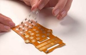
Membrane Switch Prototype Design
There are a plethora of design choices, materials, and other considerations to weigh in membrane switch design. Even the most well-thought-out plans sometimes aren’t as functionally adequate when they’re brought to fruition, making membrane switch prototypes a critical component of the overall design process. By first creating a prototype, the look, feel, and functionality of the final product can be truly evaluated in near real-world conditions. Ideally, the prototype is as close to the final product as possible, leaving only a few minor tweaks, if any adjustments are necessary at all.
For these reasons and more, an experienced membrane switch design team is invaluable to product manufacturers. It’s not cost-effective in terms of time or money to produce dozens of prototypes, each with minor improvements over the last but still falling short of the ideal product. The following outlines the basic considerations that should be weighed throughout the membrane switch prototype design process.
Membrane Switch Materials and Substrates
From rubber keypads to fully integrated, turnkey assemblies, there are a variety of materials and substrates to consider based on the type of membrane switch assembly you require and your product’s specifications. Membrane switches range from PCB membrane switch keypads to copper flex circuit membrane switches, silver flex circuit membrane switches, DuraSwitch and even touch screen options.

Rigid support backers, such as aluminum and FR4, are sometimes desirable to provide structure and rigidity to your membrane switch assembly. Materials and substrates play an integral role in the ultimate functionality of your product, offering tactile feedback, texturing, and other elements that, combined, produce the desired look, feel, and functionality. The careful selection of materials should be considered heavily in the design of every component, from selecting rigid backers to choosing the appropriate substrate (such as polyester or polycarbonate) for the graphic overlay.
Membrane Switch Backlighting
Backlighting is an important consideration in membrane switch prototype design. For products that may be used in dim lighting conditions, backlighting adds usability to a product’s user interface.
There are several backlighting options that may be used in membrane switch prototype design, including embedded LEDs, fiber optic backlighting, and electroluminescent (EL) backlighting. Each type of backlighting offers pros and cons, such as durability and ease of replacement. Other considerations include the ease of implementation given the design requirements and layout.
Graphic Overlays
The graphic overlay is the visual interface component of a membrane switch assembly, providing the look and feel of the final product. Graphic overlays can be screen printed or digitally printed, based on the desired effects such as colors, shading, three-dimensional graphics, and other considerations.
Digital printing provides some key advantages in the printing of graphic overlays. In addition to a broader range of effects, including photo-quality printing, digital printing eliminates the added expense of films and screens which are required for more traditional printing methods, such as screen printing.
Textures, embossed areas, transparent windows, backlighting, and dead front or white front images are all considerations in designing the graphic overlay component of a membrane switch assembly.
Tactile Feedback
Tactile feedback plays an increasingly important role in product usability, as tactile feedback options have evolved from the traditional feedback provided by standard keypads to a variety of feedback options with varying actuation force requirements. As such, tactile feedback is an important consideration in membrane switch prototype design and this single consideration can make or break a product’s success on the market.
Tactile feedback can be created with the use of stainless steel domes and other structures embedded in the membrane switch assembly. If tactile feedback elements will be used in the membrane switch prototype design, this impacts other design considerations such as overlay thickness. An overlay that is too thick may reduce the tactile feedback provided by domes, producing an effect other than the precise effect desired.
Membrane Switch Circuit Layers

Many product manufacturers believe that the graphic overlay component is the most important component of a membrane switch assembly. While the graphic overlay provides the look and feel of the product, the visual interface through which the end user interacts with and controls a device, the graphic overlay is ineffective without the proper underlying components that provide the functionality and reliability necessary for the product to work as desired.
The circuit layer component, therefore, is equally as important as the graphic overlay and other components in providing the final form and function of a membrane switch assembly. It’s the circuit layer (or layers) that enable the device’s connectivity. Poly domes are sometimes integrated within a circuit layer to add tactile feedback, and the circuit layers contain conductive inks and dielectric inks printed on a polyester backer, offering core functionality and/or serving as an interconnect to controller printed circuit boards (PCBs) or other electronics.
EMI/RFI Shielding
Electromagnetic Interference (EMI) and Radio Frequency Interference (RFI) are two terms that are sometimes used interchangeably. Both refer to disturbances that have an impact on the functionality of an electronic circuit, which, in the most severe cases can lead to a complete wipe-out of data. EMI/RFI shielding is a process that protects circuits from this interference, ensuring the longevity of a device by reducing interference through the use of magnetic or conductive materials that block the field.
EMI/RFI shielding is often used in membrane switch assemblies in order to prevent outside interferences from other devices or influences from impacting the product’s functionality.
Within these considerations and others are a multitude of specifications and additional considerations. Choosing the right materials, components, and design options for a membrane switch prototype depends on product specifications, space constraints, typical use environment, end user characteristics, and a variety of other variables. The many elements, components, and options available can quite simply be overwhelming even to experienced product manufacturers.
Working with an experienced membrane switch design team to select the right options for your membrane switch prototype design will result in a prototype that closely matches the desired final product .
Example Heat Switch :

Schematic of the thermal switch showing the (a) ON-state with the liquid metal droplet bridging the heat source and sink and (b) OFF-state with liquid metal removed from the channel. (c) Side view image of the fabricated thermal switch device. (d) The ON and OFF thermal resistance circuits based on a 1-D heat transfer model.
Switches are used to control many technical products and engineered systems. Mechanical switches are used to lock or unlock doors, or to select gears in a car's transmission system. Electrical switches are used to turn on and off the lights in a room. At a smaller scale, electrical switches in the form of transistors are used to turn electronic devices on and off, or to route logic signals within a circuit.
Engineers have long desired a switch for heat flows, especially in electronics systems where controlling heat flows can significantly improve system performance and reliability. There are however significant challenges in creating such a heat switch."Heat flow occurs whenever you have a region of higher temperature near a region of lower temperature .
"In order to control the heat flow, we engineered a specific heat flow path between the hot region and cold region, and then created a way to break the heat flow path when desired."
"The technology is based on the motion of a liquid metal droplet," "The metal droplet can be positioned to connect a heat flow path, or moved away from the heat flow path in order to limit the heat flow." The researchers demonstrated the technology in a system modeled after modern electronics systems. On one side of the switch there was a heat source representing the power electronics component, and on the other side of the switch, there was liquid cooling for heat removal. When the switch was on, they were able to extract heat at more than 10 W/cm2. When the switch was off, the heat flow dropped by nearly 100X. the next step for the research is to integrate the switch with power electronics on a circuit board. The researchers will have a working prototype later this year.
prototype Switch Interface contained within a compact enclosure

EMC (electromagnetic compatibility)
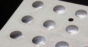
Dome Arrays
metal dome arrays, called Peel-N-Place™ Arrays, are pre-loaded polyester dome carriers backed with pressure sensitive adhesive. Arrays come loaded with the dome(s) of your choice, cut to the size and shape that you specify. Whether your circuit board is populated with one metal dome or one hundred metal domes, our Peel-N-Place™ arrays help reduce your labor costs by easing the assembly process.
 Standard Peel-N-Place
- Individual domes on a square piece of adhesive
- 1 per square, 15 to 30 per sheet depending on the dome size
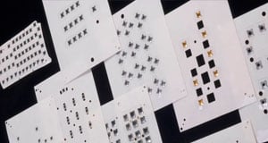 Custom Peel-N-Place
- Domes placed on sheet or reel according to your specific requirements
Peel-N-Place™ domes are attached to a square of pressure sensitive adhesive tape.
Each individual dome is peeled off the release liner backing and will adhere securely to a circuit board, flex circuit, or membrane. You can specify many of our F-Series, U-Series, P-Series or M-Series domes in standard Peel-N-Place. For other dome styles in Standard PNP format, please contact Snaptron.
Standard Peel-N-Place™ (Four Leg) dome arrays were designed specifically for mounting on printed circuit boards, flex circuits and membranes. They are individual domes backed with a square of polyester-adhesive. Each individual dome is then peeled off the release liner and is placed onto a circuit board, flex circuit or membrane with the polyester-adhesive serving to hold the dome in place. You specify the standard four-legged Snaptron dome that best suits your needs. Our application specialists can help you with your specific requirements. Two 4-leg domes can also be STACKED in a single position to double actuation force.
Our Standard Peel-N-Place™ (Four Leg) dome arrays are manufactured entirely in Windsor, Colorado, to our exacting specifications to ensure that you always receive the highest quality product with consistent characteristics every time you order.
| .375" Sq | .375" Sq | .375" Sq | .500" Sq | .562" Sq | .750" Sq | .850" Sq |
|---|---|---|---|---|---|---|
| |  |  | ||||
| PNP-05 5mm Dome Dia. 30/Sheet | PNP-06 6mm Dome Dia. 30/Sheet | PNP-07 7mm Dome Dia. 30/Sheet | PNP-08 8.5mm Dome Dia. 30/Sheet | PNP-10 10mm Dome Dia. 30/Sheet | PNP-12 12mm Dome Dia. 20/Sheet | PNP-14 14mm Dome Dia. 15/Sheet |
| Part Number Description |
|---|
| PNP-XX (ZZZZZZ) X=Dome diameter in inches Z=Standard F-Series or U-Series dome part number Ex: PNP-08 (F08400) |
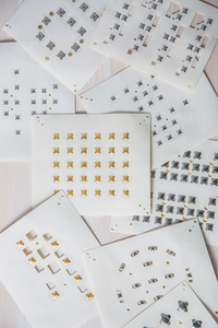 Custom Peel-N-Place™ Arrays are pre loaded polyester dome carriers backed with pressure sensitive adhesive. Arrays come loaded with the dome(s) of your choice, cut to the size and shape you specify. Different sizes, shapes, and forces of metal domes can be placed on the same array.
The standard carrier material is polyester but this can be altered to fit your needs. Placement of the array is quick and easy. Simply peel off the backing, align the array and apply it to your circuit board or membrane. Since all of the domes are placed simultaneously, production time is greatly reduced. Your quality also benefits from the use of our custom arrays which reduces the chances of “double domes” and dome placement errors. For applications that require high actuation forces, intentional STACKED metal domes (two domes per position) are available.
In order to start the process of designing a Custom Peel-N-Place™ array, here’s what we need from you:
 A drawing / print of what the part will look like. Please include overall size, dome part number(s), locations of domes and cutouts.
- Estimated annual usage of the part.
- AutoCAD (all versions)
- DXF (all versions)
- Solidworks (all versions)
- Inventor (.ipt)
- Solid Edge (.par)
- IGES (all versions)
- STEP (all versions)
- ACIS (.sat)
- Parasolid (all versions)
- Catia Graphics (.cgr)
- STL (.stl)
- VDASF (.vda)
- Acrobat (.pdf)
There are two packaging options to choose from:
Custom Peel-N-Place™ array sheets are pre-loaded polyester dome carriers backed with pressure-sensitive adhesive. The standard carrier is polyester, but this can be altered to fit your needs. Our array sheet design lends itself well to low and medium volume applications, where cost savings is critical during the board assembly process.
Note: Standard sheet format sizes available are: 5.3″ x 4.5″, 7″ x 8″. For information about custom sizes, please contact Snaptron.
Placement of the Peel-N-Place™ arrays is quick and easy. Simply peel off the release liner, align the array and apply it to your circuit
board, flex circuit, or membrane. Snaptron also offers CUSTOM FIXTURES to assist you in the placement process. Two 4-leg domes can also be STACKED in a single position to double actuation force. By placing all of the domes simultaneously, production time is greatly reduced. Your quality also benefits from the use of our custom arrays which eliminate “double domes” and dome placement errors.Our Custom Peel-N-Place™ dome arrays are manufactured entirely in Windsor, Colorado, to our exacting specifications to ensure that you always receive the highest quality product with consistent .
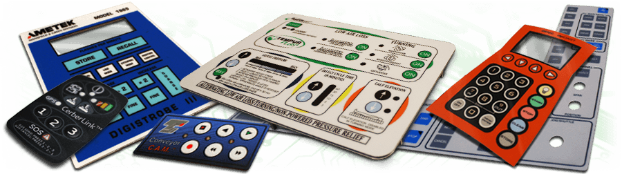
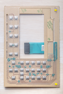
Membrane Switches
keypads, control panels, touchpads, switch assemblies
As the man-machine interface, the membrane switch is often the most important part of a piece of equipment. It showcases the quality and workmanship put into an assembly and has been proven to be a determining factor in purchasing decisions.
From the early stages of development, material selection and design, SelecTouch is there, offering complete design for both the switch and graphics. Our state-of-the-art model shop offers 3 to 5 day turn-around on most prototypes without costly hard tooling! Tactile or non-tactile, metal or poly dome, each switch will withstand millions of cycles.
Five, ten, and twenty plus years down the road, SelecTouch quality membrane switches hold up in harsh environments. On gas pumps, electronic equipment, handheld consumer devices and more .
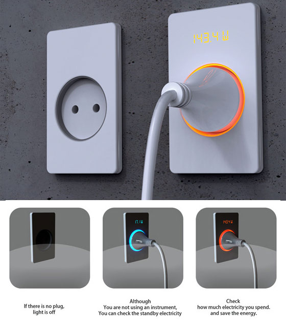
XXX . XXX Innovative and Cool Electrical Outlets, Sockets and Switches
With the modernization of our life, we have more and more electronics at home, which means more and more Electrical Outlets, Sockets and Switches to get them plug in .
Sockets and Switches designs we rounded up which could help you keep the wire mess in check, save some energy and accomordate more crowded plugs. Too bad some of them are still concepts.
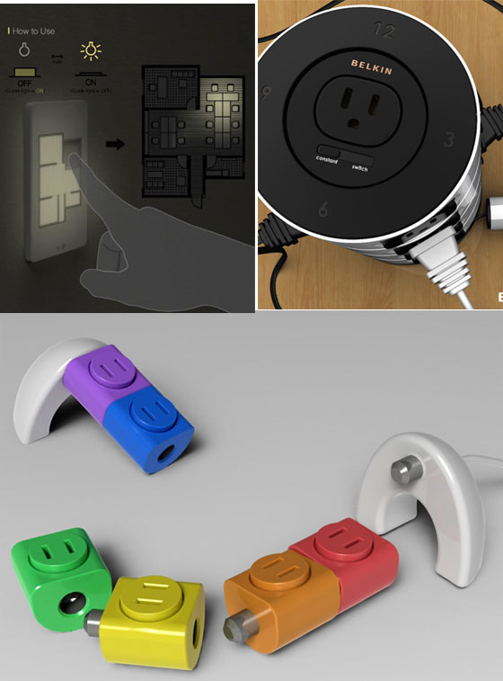
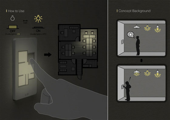
1. Floor Plan Light Switch
When you have a panel full of light switches, it can be challenging to remember which is which. The Floor Plan Light switch offers an easy solve. The switches are modified according to the floor plan of the room and operate accordingly. So in a single glance you know which switch controls what.
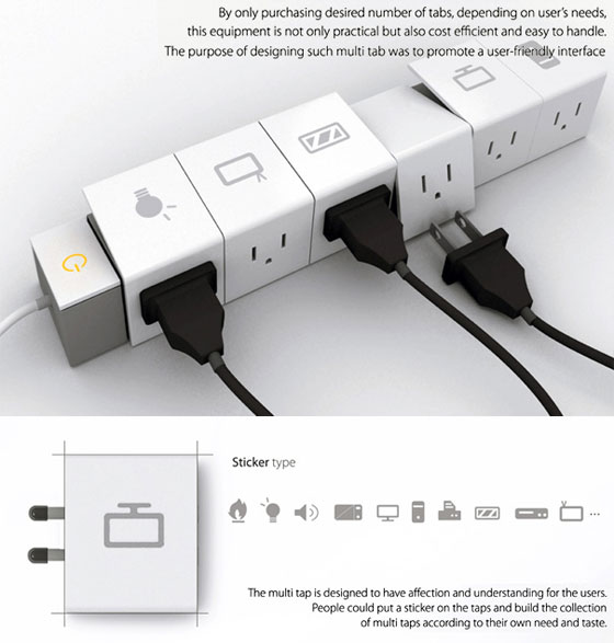
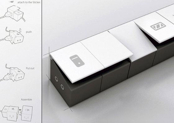
2. Tab The Power Strip
This crazy thing takes aid of pictogram and energy efficient LED lights to help you keep a track of your hooked up gadgets. Unwanted tabs and sockets easily detach with a tug-up on the tab! Users can configure the power strip with as many or as few outlets required.
3. Show-off The Strip
Managing power-cords is more of a hassle for folks with kids and those who like the wire-free look. Just how to manage those damn wires? With the elegant Power Bridge, of course! It eliminates the need to hide wires in order to make the room look neat or safe. This sturdy strip has the plug-slots beneath the bridge for better plug management. An indicative light on each plug outlet also displays the amount of power being used by that particular device, making you aware of the energy consumption. A refreshing approach for the wires-issue.

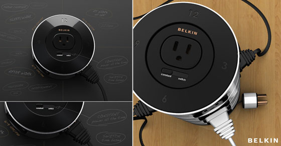
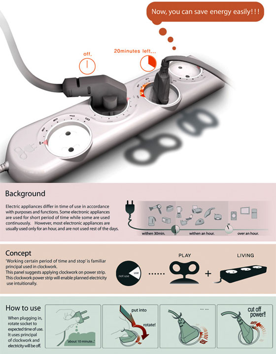
4. Put Your Power On A Timer
The Belkin Time Outlet concept is a modular, stackable surge protector divided into 4 quadrants. Each section corresponds to a time of day. When that time is over, power is cut from everything in that quadrant and power turns on in the next.
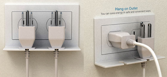
5. Hang On Outlet
Hang On Outlet – is a basic power outlet with a little extra lip to hold on to your lose plugs, keeping your power management neat and tidy.
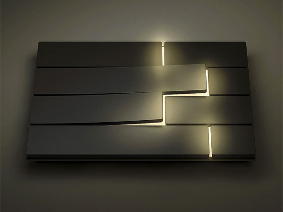
6. Remorkable Piano Switches
A Frame-less switch was an important driver for the new design. David Dos Santos’ design is clean, sober, simple. The sort of soft piano keys you want to touch. This distinctive form has the rare property of being in perfect equilibrium with its surroundings, whether the style is modern or classic.
Piano is really versatile; it can be combined with almost any RAL colour.To customize the switches, text or symbols can be screen printed or engraved onto the switches. This ensures that each product is unique. A LED module can be used to create stylish effect, that allows it to enlighten the switch, functions and surroundings in a distinctive fashion.
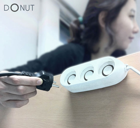
7. Donut Power Strip
The Donut power strip by Ramei Keum solves the annoyances with most power strips today, namely not accommodating the huge power bricks that come with many of our electric appliances. Each outlet can spin inside its socket for the best fit. The donut shape also helps to keep cabling organized.
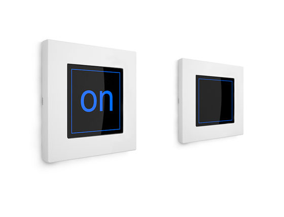
8. On Switch
Russian designer Burakov Denis has offer the concept to make people realize that the light switch in their house is still on. With the clear and big “ON” letter, it should reminds people to turn them OFF when they’re not in used.
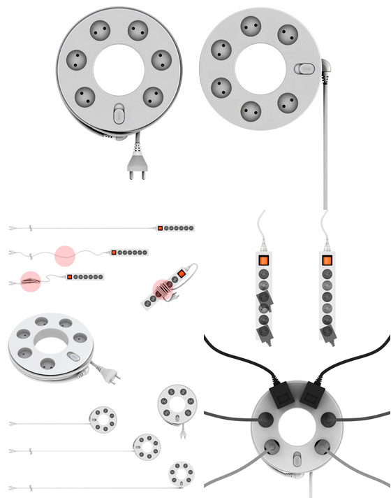
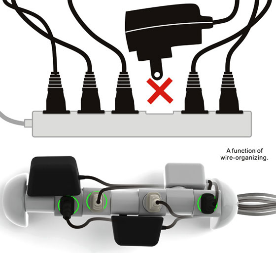
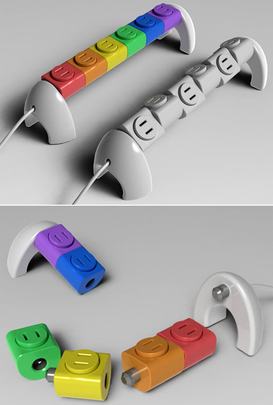
9. Rotating 360 degree Lego Sockets
Rotating 360 degree is a multi-outlet socekt which allows each socket on it to rotate. It offers enough space for different shaped plugs to plug in just by rotating each socket in different directions. Besides, each socket has different color and can connect each other, so user can easily increase or decrease the number of sockets for his or her multi-outlet socekt and choose different colors depends on user’s end. In addition, there are 2 standing base on both ends of this product to provide a function of wire-organizing.
10. Wireless Nano grid Switches
A light switch that draws inspiration from traditional Korean architecture (and clothing!) These switches (for electricity) are capable of not only switching the lights on and off, they can deliver detailed info about the energy usage of the room they’re installed in via free web or smartphone applications. Temperature sensors, imaging equipment, and more are available additions to the Nanogrid structure.
11. Smile Switches
Simply use the emotional expression to remind and educate users to turn off the light.
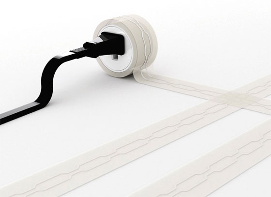
12. Post Line – No More Trippin Wires
The thing with extension cords is that they look ugly and the wires are a prime accident zones for tripping. There is nothing Elegant about them! Unless you’re looking at the Post Line? this one’s a gorgeous concept that makes full use of the circuit-printing technology and electrostatic paste material. Use it from point A (gadget) to point B (wall socket) by sticking it flat to the floor, and if it becomes less sticky and grimy, simply wipe it clean and its sticky flat extension tape again!
13. Rozetkus – Three Dee Power Socket
Hiding in the wall until the right moment to strike, the Rozetkus sits flat unless more than one plug is needed.
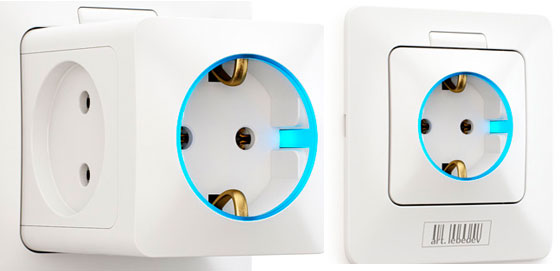
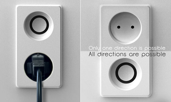
14. DONUT – The Any Way Socket
It’s clever of us to hide socket boards behind furniture and out-of-sight places, however plugging up lamps or devices is another story altogether! Aligning the plug prongs can be a challenge and Donut resolves this issue. The socket allows you to hook up the plug in a ring-shaped hole? so that it can be inserted at any angle. As the red dot winning designers say, here is no need to align the pins with two specific small holes.
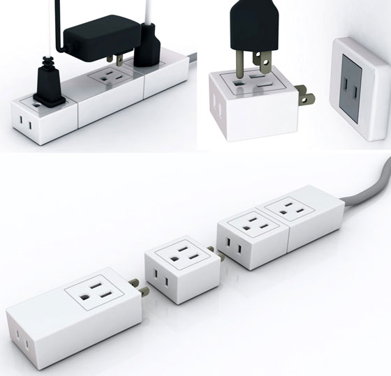
15. Too Many Sockets Make a Brick
Socket Like Brick allows you to configure and create a modular multi-tap as per convenience. Extend or remove modules safely, moreover accommodate the different sized plugs with ease. It basically provides a good solution to the managing devices.
16. Insic Wall Socket
This is a plug for the world to become more environmentally friendly. It’s a plug you plug into the wall to access power, but not just that! No way, that’s too simple. This one lights up in a way that shows you the way, the truth, and the light! This insic Wall Socket?encourages you to use power only so long as you need it. This isn’t just a dormant tool, nay, this one encouraging you to be the green crusader you’re always aspired to be.
17. Wind Up With Glee
Putting it straight enough for you, Wind Up Socket has a timer to it, once you set the duration and time up, the electricity supply to that socket gets cut off. For grownups who don’t have many restrictions and can self regulate, this one may seem more cumbersome than anything else.
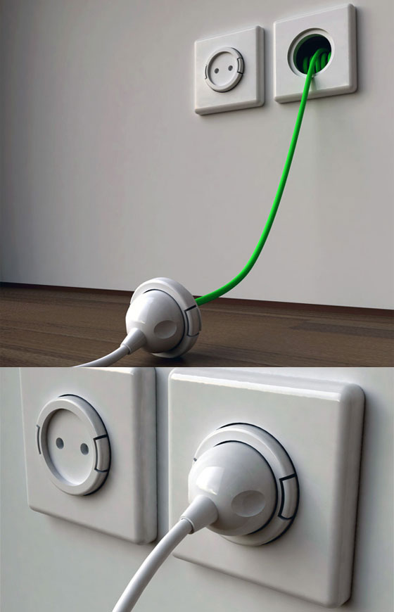
18. Rambler Socket – Recoiling Socket In The Wall
Rambler Socket has 1.5 meters cord that unfurls from a cavity behind its socket. When you don’t need extensions, it’s neatly tucked away. When you need it, simply pinch the sides and wind it out. After the deed is done, you simply give the wire a gentle tug (activates a spring mechanism), and it recoils back into place. Ideal for using with electronics like vacuum cleaners, hair driers etc where you don’t need extension cords on a full-time basis.
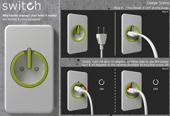
19. Power Socket SWITCH
Keep getting to slammed for not switching off the mains or unplugging your gadgets? It’s not that people are reckless or unconcerned about the environment, but sometimes simple and easy things like this becomes too much of an effort. So should we mop around for allowing Stand-By Power to contribute to almost 11% of our monthly electricity bill?
Review a traditional Switch
What we see here is the basis for switching lamps on and off by remote switches. Because any break in a circuit’s continuity results in current stopping throughout the entire circuit, we can use a device designed to intentionally break that continuity (called a switch), mounted at any convenient location that we can run wires to, to control the flow of electrons in the circuit:

This is how a switch mounted on the wall of a house can control a lamp that is mounted down a long hallway, or even in another room, far away from the switch. The switch itself is constructed of a pair of conductive contacts (usually made of some kind of metal) forced together by a mechanical lever actuator or pushbutton. When the contacts touch each other, electrons are able to flow from one to the other and the circuit’s continuity is established; when the contacts are separated, electron flow from one to the other is prevented by the insulation of the air between, and the circuit’s continuity is broken.
Perhaps the best kind of switch to show for illustration of the basic principle is the “knife” switch:

A knife switch is nothing more than a conductive lever, free to pivot on a hinge, coming into physical contact with one or more stationary contact points which are also conductive. The switch shown in the above illustration is constructed on a porcelain base (an excellent insulating material), using copper (an excellent conductor) for the “blade” and contact points. The handle is plastic to insulate the operator’s hand from the conductive blade of the switch when opening or closing it.
Here is another type of knife switch, with two stationary contacts instead of one:

The particular knife switch shown here has one “blade” but two stationary contacts, meaning that it can make or break more than one circuit. For now this is not terribly important to be aware of, just the basic concept of what a switch is and how it works.
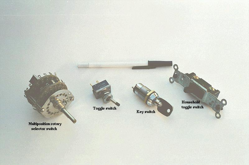
Knife switches are great for illustrating the basic principle of how a switch works, but they present distinct safety problems when used in high-power electric circuits. The exposed conductors in a knife switch make accidental contact with the circuit a distinct possibility, and any sparking that may occur between the moving blade and the stationary contact is free to ignite any nearby flammable materials. Most modern switch designs have their moving conductors and contact points sealed inside an insulating case in order to mitigate these hazards. A photograph of a few modern switch types show how the switching mechanisms are much more concealed than with the knife design:
In keeping with the “open” and “closed” terminology of circuits, a switch that is making contact from one connection terminal to the other (example: a knife switch with the blade fully touching the stationary contact point) provides continuity for electrons to flow through, and is called a closed switch. Conversely, a switch that is breaking continuity (example: a knife switch with the blade not touching the stationary contact point) won’t allow electrons to pass through and is called an open switch. This terminology is often confusing to the new student of electronics, because the words “open” and “closed” are commonly understood in the context of a door, where “open” is equated with free passage and “closed” with blockage. With electrical switches, these terms have opposite meaning: “open” means no flow while “closed” means free passage of electrons.
XXX . XXX 4%zero null 0 Light switch

Light switches are also found in flashlights and automobiles and other vehicles.
Wall-mounted switches
Switches for lighting may be in hand-held devices, moving vehicles, and buildings. Residential and commercial buildings usually have wall-mounted light switches to control lighting within a room. Mounting height, visibility, and other design factors vary from country to country. Switches are often recessed within a finished wall. Surface mounting is also fairly common though is seen more in commercial industrial and outbuilding settings than in houses. A light switch box (a pattress box) has a plastic, ceramic, or metal cover to prevent accidental contact with live terminals of the switch. Wall plates are available in different styles and colours to blend in with the style of a room. They are though quite easy to mount.History, culture, and style

The toggle light switch was invented in 1917 by William J. Newton.
As a component of an electrical wiring or home wiring system, the installation of light switches is regulated by some authority concerned with safety and standards. In different countries the standard dimensions of the wall mounting hardware (boxes, plates, etc.) may differ. Since the face-plates used must cover this hardware, these standards determine the minimum sizes of all wall mounted equipment. Hence, the shape and size of the boxes and face-plates, as well as what is integrated, varies from country to country.
The dimensions, mechanical designs, and even the general appearance of light switches has changed slowly over time. Switches typically remain in service for many decades, often being changed only when a portion of a house is rewired. It is not unusual to see century-old light switches still in functional use. Manufacturers introduce various new forms and styles, but for the most part decoration and fashion concerns are limited to the face-plates or wall-plates. Even the "modern" dimmer switch with knob is at least forty years old, and in even the newest construction the familiar toggle and rocker switch formats predominate.
Orientation
The direction which represents "on" also varies by country. In the US and Canada, it is usual for the "on" position of a toggle switch to be "up", whereas in many other countries such as the UK, Ireland, Australia, and New Zealand it is "down". (In multiway switching, the correspondence between a single switch's state and whether lights are on or off depends on the state of the other switch[es] in the circuit.)Design
The switches may be single or multiple, designed for indoor or outdoor use. Optional extras may include dimmer-controls, environmental protection, weather and security protection. In residential and light commercial lighting systems, the light switch directly controls the circuit feeding the lamps. In larger lighting systems, for example warehouses or outdoor lighting systems, the required current may be too high for a manual switch. In these systems light switches control lighting contactors, a relay that allows the manual light switch to operate on a lower voltage or with smaller wiring than would be required in the main lighting circuit.In the UK, putting 13 Amp BS1363 sockets on a lighting circuit is discouraged (although not outright prohibited), but 2 Amp or 5 Amp BS546 outlets are often put on lighting circuits to allow control of free-standing lamps from the room's light switches. In North American site-built and mobile homes, often living rooms and bedrooms have a switched receptacle for a floor or table lamp.
Internal operation
The contacts of a switch are under their greatest stress while opening or closing. As the switch is closed, the resistance between the contacts changes from almost infinite to almost zero. At infinite resistance, no current flows and no power is dissipated. At zero resistance, there is no voltage drop and no power is dissipated. However, while the contacts change state, there is a brief instant of partial contact when resistance is neither zero nor infinite, and electrical power is converted into heat. If the heating is excessive, the contacts may be damaged, or may even weld themselves closed.A switch should be designed to make its transition as swiftly as possible. This is achieved by the initial operation of the switch lever mechanism storing potential energy, usually as mechanical stress in a spring. When sufficient mechanical energy is stored, the mechanism in the switch "breaks over", and quickly drives the contacts through the transition from open to closed, or closed to open, without further action by the switch operator. This quick-break action of the switch is essential to a long life for the switch contacts, as described in Holmes' 1884 patent.
While the contacts are separating, any electrical energy stored in the inductance of the circuit being disconnected is dissipated as an arc within the switch, prolonging the transition and worsening the heating effect on the contacts. Switches are commonly rated by the current they are designed to break, under specified voltage and power factor conditions, as this is the most stringent limitation.
The arc that results when the switch opens erodes the switch contacts. Therefore, any switch has a finite life, often rated at a given number of cycles of disconnection at a specified current. Operation outside of its specified operating capacity will drastically shorten the life of the switch.
To combat contact corrosion, a switch is usually designed to have a "wipe" action so that the contacts are cleaned. Large switches may be designed with a supplemental replaceable contact that closes and opens before the main contact, protecting the main current-carrying contacts from wear due to arcing. The contact area of the switch is constructed of materials that resist corrosion and arcing.
Many higher current switch designs rely on the separation arc to assist in dispersing contact corrosion. A switch designed for high-current high-voltage use may become unreliable if operated at very low currents and low voltages, because a non-conductive oxide layer builds up without an arc to disperse it.
Two kinds of sparks may occur during switch operation. On closure, a few sparks, like those from a flint-and-steel, may appear as a tiny bit of metal is heated by friction to incandescence, melted, and thrown off. On opening, a bluish arc may occur, with a detectable "electrical" (ozone) odor. Subsequently, the contacts may be seen to be darkened and pitted. Damaged contacts have higher resistance, rendering them more vulnerable to further damage and causing a cycle in which the contacts soon may fail completely.
To make a switch safe, durable, and reliable, it must be designed so that the contacts are held firmly together under positive force when the switch is closed. It should be designed so that, regardless of how the operator manipulates the actuator, the contacts always close or open quickly.
In the construction of many small switches, the spring that stores the mechanical energy necessary for the snap action of the switch mechanism is made of a beryllium copper alloy that is hardened to form a spring as part of the fabrication of the contact. The same part often also forms the body of the contact itself, and is thus the current path. Abusing the switch mechanism to hold the contacts in a transition state, or severely overloading the switch, will heat and thus anneal the spring, reducing or eliminating the "snap action" of the switch, leading to slower transitions, more energy dissipated in the switch, and progressive failure.
Variations on design
Push button
The push-button light switch has two buttons: one that closes the contacts and one that opens the contacts. Pushing the raised button opens or closes the contacts and pops out the previously depressed button so the process can be reversed. Push-button switch reproductions are available on the market today for vintage or authentic styling.
Toggle
The toggle mechanism provides "snap-action" through the use of an "over-center" geometry. The design was patented in 1916 by William J. Newton and Morris Goldberg. The switch actuator does not control the contacts directly, but through an intermediate arrangement of springs and levers. Turning the actuator does not initially cause any motion of the contacts, which in fact continue to be positively held open by the force of the spring. Turning the actuator gradually stretches the spring. When the mechanism passes over the center point, the spring energy is released and the spring, rather than the actuator, drives the contacts rapidly and forcibly to the closed position with an audible "snapping" sound. This mechanism is safe, reliable, and durable, but produces a loud snap or click.

As of 2004[update] in the United States, the toggle switch mechanism was almost entirely supplanted by "quiet switch" mechanisms. "Quiet switch" mechanisms still possess a form of snap action, but it is very weak as compared to its predecessor. They are therefore equipped with larger, high-quality contacts that are capable of switching domestic loads without damage, despite the less-positive action.
Illuminated switch
Illuminated switches incorporate a small neon lamp or LED, allowing the user easily to locate the switch in the dark. Household illuminated switches were introduced in the mid-1950s.
Single-pole illuminated switches derive the power to energize their in-built illuminating source (usually, a "neon" lamp) from the current passing through the lamp(s) which they control. Such switches work satisfactorily with incandescent lamps, halogen lighting, and non-electronic fluorescent fixtures, because the small current required for the switch's illuminating source is too small to produce any visible light from such devices controlled by the illuminated switch. However, if they control only compact fluorescent lamps (CFLs) and/or LED lamps, the small amount of current required to energize the lighting source within switch also slowly charges the internal input capacitor in the electronic ballast of the CFL or LED until the voltage across it rises to the point where it produces a brief discharge through the CFL. This cycle may repeat indefinitely, resulting in repetitive brief flashing of the lamp(s) (and the light inside the switch) while the illuminated switch is in the "off" position.
Rocker
An alternative design to the toggle switch is the rocker switch. Large switches of this design are commonly known as "decorator style" in the United States Switches of this design sit almost flush with the wall plate, and are activated by "rocking" a flat, broad lever, rather than pushing a short protruding actuator up or down.

In Europe, Hong Kong, Malaysia, Singapore, and India this type is near-universal, and toggle style switches would be considered old-fashioned
Australian rocker switches


While larger "decorator" style switches are readily available in Australia, the advantage of the smaller mechanisms is that wall-plates are available to mount from one to six individual switch mechanisms, or other correspondingly sized "mechanisms" - such as dimmers and indicator lights - in the same space as one (or two) switches of larger design could be mounted. Since the mechanisms are small, they can also be mounted into "architrave" plates, for mounting in positions where it is not possible to mount a "standard" sized wall-plate. An example is shown in the picture below on the right. All of the switch mechanisms have no exposed metal parts requiring grounding (earthing). While switches, wall-plates, and cover plates from different manufacturers tend not to be interchangeable, switch mechanisms of this type have been available in Australia since 1971.
The keystone module system for extra-low voltage electrical jacks (patented in 1995) is somewhat similar in appearance to these modules, but the design of the keystone mountings are different, and keystone modules can be removed without a tool. (A similar system, but with bigger switches, is used in Italy.)
As shown in the disassembly photo, the switch actuator pivots in two holes in the sides of the plastic switch body. An actuator bar slides in two grooves inside the actuator, pressed down by a compression spring into a notch in the common contact bar. The common contact bar is free to rock on a small diameter rod, welded to the common terminal. However, because of the pressure applied by the compression spring, the common contact bar will always be held against one of the two contacts.
When the actuator is moved, mechanical energy is stored in the compression spring until the actuator passes its mid-position. At that time, the common contact bar is forced in the opposite direction by the compression spring, acting via the actuator bar, thus breaking the connection with the existing contact and making connection with the other contact. The common contact bar is made of copper, with an inlay of harder contact metal on the underside. While it is free to move the required distance lengthwise, it is constrained from moving sideways by the construction of the molded plastic body.
The screw terminals are hollow and allow up to at least three 1 mm (CSA) wires, twisted together, to be inserted to a depth of up to 10 millimetres (0.39 in) and secured with a set screw. The contact terminal set screws are installed at a slight angle to allow easier screwdriver access after the switch mechanism has been installed into a wall-plate - before fixing the wall-plate to the wall. Also shown is a "loop" connection terminal. This terminal plays no part in the action of the switch but, because there is available space, it is provided as an insulated terminal for joining other wires, if required (such as the neutral wires). Each Australian rocker switch mechanism is actually a single-pole, double-throw (SPDT) Switch, also known as a "two-way switch", and has three terminals.
A switch of basically the same design is also used on Australian power outlet wall-plates. It is now extremely rare to find any other type of switch in Australian homes, although the Australian Wiring Standard AS 3112 does not forbid other types. While many variations of Australian designs and cover plates are available, some designers and renovators may import UK- and European-designed switches when they desire a particular finish. However, while standard Australian wall mounting plates have the same dimensions as those used in North America, they have different dimensions from those used in the UK or Europe.
Switches (and other mechanisms) of this Australian design series are currently available in the UK (and other countries), together with wall-plates appropriate to the mounting standards of the countries concerned.
For a short time, Australian rocker switches were exported to the United States in the 1980s. Although the switches had adequate ratings for usage on 120 V circuits and had advantages of compactness and distinctive appearance, they failed to establish themselves in the American market.
Tamper resistant

Voltage class
In North American commercial and industrial lighting installations, lighting installed on 480Y/277 V 3-phase circuits uses voltages higher than the rating of common 120 V switches.Mercury switch
Before the 1970s, mercury switches were popular. Their cost was more than that of other designs, but they were totally silent in operation. The switch actuator tipped a sealed glass vial connected via flexible leads, causing a drop of liquid metallic mercury to roll from one end to the other. When it arrived at the contact end, the drop of mercury bridged a pair of contacts to complete the circuit. Many of these switches were also equipped with a neon lamp connected across the contacts, and thus in series with the electrical load. This caused the indicator to glow faintly when the switch was off, as an aid to finding the switch in a dark room.

Although the glass vial was hermetically sealed, concerns about the release of toxic mercury when the switches were eventually damaged or disposed of led to the abandonment of this design for new products.
Pull-chain or pull-cord
A light switch combined with a light socket is sometimes installed in basement or utility areas of homes. The switch is operated by a pull chain or cord. It is also possible to have the cord-operated switch separate from the light socket, which is particularly common in British bathrooms. Until 2001, UK wiring regulations required that all bathroom switches were operated by pull cords.Dimmer switch
A dimmer switch, properly called a dimmer control, contains a solid-state circuit to allow changing the brightness by reducing the average voltage applied to the lamp.Electronic switches
In principle, it is easy to design silent switches in which the mechanical contacts do not directly control the current, but simply signal a solid-state device such as a thyristor to complete the circuit. Many variations on this theme have been created and marketed. "Touch-plate" devices can be operated by touching or merely waving a hand near the switch. Touch switches have no moving parts and electronically switch the light circuit. As of 2006[update] these remain specialty items. Electronic switches provide flexibility in terms of different interfaces for their operations, such as touch plates, soft-touch controls, pressure or light sensor based control, interactive touch-screens (which are widely used in aircraft for lighting control), and others.
Public buildings such as hospitals frequently save energy by using motion detector switches, also known as occupancy sensors. The occupancy sensors can also be used in residential applications such as in bathrooms, garages, and hallways.
A wireless light switch provides remote control of lighting using a hand-held transmitter. While the controlling device may be a unit dedicated to this purpose, increasingly such switches may be controlled by the technology (such as Bluetooth or Wi-Fi) now found in smartphones.
Wired remote control of lighting switches is also possible using, for example, X10 signaling over the power wires.
Multiway switching
Two or more light switches can be interconnected to allow control of lighting from, for example, two ends of a long hallway or landings at the upper and lower landings of a flight of stairs. Multiway switching is done using special switches that have additional contacts.Materials
Earlier switches were made of porcelain in the surface-mounted version and operated as a rotary switch with a rotary mechanism. Later, more durable Bakelite was used. Today they are made of modern plastics. In some cases, especially in hospitals and other public facilities, exposed parts of light switches are made of antimicrobial materials such as copper, for infection control.XXX . XXX 4%zero null 0 1 2 3 4 Semiconductor device : it's mean electronics switches or a processing component on electronics circuit
Semiconductor devices are electronic components that exploit the electronic properties of semiconductor materials, principally silicon, germanium, and gallium arsenide, as well as organic semiconductors. Semiconductor devices have replaced thermionic devices (vacuum tubes) in most applications. They use electronic conduction in the solid state as opposed to the gaseous state or thermionic emission in a high vacuum.
Semiconductor devices are manufactured both as single discrete devices and as integrated circuits (ICs), which consist of a number—from a few (as low as two) to billions—of devices manufactured and interconnected on a single semiconductor substrate, or wafer.
Semiconductor materials are useful because their behavior can be easily manipulated by the addition of impurities, known as doping. Semiconductor conductivity can be controlled by the introduction of an electric or magnetic field, by exposure to light or heat, or by the mechanical deformation of a doped monocrystalline grid; thus, semiconductors can make excellent sensors. Current conduction in a semiconductor occurs via mobile or "free" electrons and holes, collectively known as charge carriers. Doping a semiconductor such as silicon with a small proportion of an atomic impurity, such as phosphorus or boron, greatly increases the number of free electrons or holes within the semiconductor. When a doped semiconductor contains excess holes it is called "p-type", and when it contains excess free electrons it is known as "n-type", where p (positive for holes) or n (negative for electrons) is the sign of the charge of the majority mobile charge carriers. The semiconductor material used in devices is doped under highly controlled conditions in a fabrication facility, or fab, to control precisely the location and concentration of p- and n-type dopants. The junctions which form where n-type and p-type semiconductors join together are called p–n junctions.
Diode
A semiconductor diode is a device typically made from a single p–n junction. At the junction of a p-type and an n-type semiconductor there forms a depletion region where current conduction is inhibited by the lack of mobile charge carriers. When the device is forward biased (connected with the p-side at higher electric potential than the n-side), this depletion region is diminished, allowing for significant conduction, while only very small current can be achieved when the diode is reverse biased and thus the depletion region expanded.Exposing a semiconductor to light can generate electron–hole pairs, which increases the number of free carriers and thereby the conductivity. Diodes optimized to take advantage of this phenomenon are known as photodiodes. Compound semiconductor diodes can also be used to generate light, as in light-emitting diodes and laser diodes.
Transistor

Operation of a MOSFET and its Id-Vg curve. At first, when no gate voltage is applied. There is no inversion electron in the channel, the device is OFF. As gate voltage increase, inversion electron density in the channel increase, current increase, the device turns on.
Bipolar junction transistor
Bipolar junction transistors are formed from two p–n junctions, in either n–p–n or p–n–p configuration. The middle, or base, region between the junctions is typically very narrow. The other regions, and their associated terminals, are known as the emitter and the collector. A small current injected through the junction between the base and the emitter changes the properties of the base-collector junction so that it can conduct current even though it is reverse biased. This creates a much larger current between the collector and emitter, controlled by the base-emitter current.Field-effect transistor
Another type of transistor, the field-effect transistor, operates on the principle that semiconductor conductivity can be increased or decreased by the presence of an electric field. An electric field can increase the number of free electrons and holes in a semiconductor, thereby changing its conductivity. The field may be applied by a reverse-biased p–n junction, forming a junction field-effect transistor (JFET) or by an electrode insulated from the bulk material by an oxide layer, forming a metal–oxide–semiconductor field-effect transistor (MOSFET).The MOSFET, a solid-state device, is the most used semiconductor device today. The gate electrode is charged to produce an electric field that controls the conductivity of a "channel" between two terminals, called the source and drain. Depending on the type of carrier in the channel, the device may be an n-channel (for electrons) or a p-channel (for holes) MOSFET. Although the MOSFET is named in part for its "metal" gate, in modern devices polysilicon is typically used instead.
Semiconductor device materials
By far, silicon (Si) is the most widely used material in semiconductor devices. Its combination of low raw material cost, relatively simple processing, and a useful temperature range makes it currently the best compromise among the various competing materials. Silicon used in semiconductor device manufacturing is currently fabricated into boules that are large enough in diameter to allow the production of 300 mm (12 in.) wafers.Germanium (Ge) was a widely used early semiconductor material but its thermal sensitivity makes it less useful than silicon. Today, germanium is often alloyed with silicon for use in very-high-speed SiGe devices; IBM is a major producer of such devices.
Gallium arsenide (GaAs) is also widely used in high-speed devices but so far, it has been difficult to form large-diameter boules of this material, limiting the wafer diameter to sizes significantly smaller than silicon wafers thus making mass production of GaAs devices significantly more expensive than silicon.
Other less common materials are also in use or under investigation.
Silicon carbide (SiC) has found some application as the raw material for blue light-emitting diodes (LEDs) and is being investigated for use in semiconductor devices that could withstand very high operating temperatures and environments with the presence of significant levels of ionizing radiation. IMPATT diodes have also been fabricated from SiC.
Various indium compounds (indium arsenide, indium antimonide, and indium phosphide) are also being used in LEDs and solid state laser diodes. Selenium sulfide is being studied in the manufacture of photovoltaic solar cells.
The most common use for organic semiconductors is Organic light-emitting diodes.
List of common semiconductor devices
Two-terminal devices:- DIAC
- Diode (rectifier diode)
- Gunn diode
- IMPATT diode
- Laser diode
- Light-emitting diode (LED)
- Photocell
- Phototransistor
- PIN diode
- Schottky diode
- Solar cell
- Transient-voltage-suppression diode
- Tunnel diode
- VCSEL
- Zener diode
- Bipolar transistor
- Darlington transistor
- Field-effect transistor
- Insulated-gate bipolar transistor (IGBT)
- Silicon-controlled rectifier
- Thyristor
- TRIAC
- Unijunction transistor
- Hall effect sensor (magnetic field sensor)
- Photocoupler (Optocoupler)
Semiconductor device applications
All transistor types can be used as the building blocks of logic gates, which are fundamental in the design of digital circuits. In digital circuits like microprocessors, transistors act as on-off switches; in the MOSFET, for instance, the voltage applied to the gate determines whether the switch is on or off.Transistors used for analog circuits do not act as on-off switches; rather, they respond to a continuous range of inputs with a continuous range of outputs. Common analog circuits include amplifiers and oscillators.
Circuits that interface or translate between digital circuits and analog circuits are known as mixed-signal circuits.
Power semiconductor devices are discrete devices or integrated circuits intended for high current or high voltage applications. Power integrated circuits combine IC technology with power semiconductor technology, these are sometimes referred to as "smart" power devices. Several companies specialize in manufacturing power semiconductors.
Component identifiers
The type designators of semiconductor devices are often manufacturer specific. Nevertheless, there have been attempts at creating standards for type codes, and a subset of devices follow those. For discrete devices, for example, there are three standards: JEDEC JESD370B in United States, Pro Electron in Europe and Japanese Industrial Standards (JIS) in JapanSemiconductors had been used in the electronics field for some time before the invention of the transistor. Around the turn of the 20th century they were quite common as detectors in radios, used in a device called a "cat's whisker" developed by Jagadish Chandra Bose and others. These detectors were somewhat troublesome, however, requiring the operator to move a small tungsten filament (the whisker) around the surface of a galena (lead sulfide) or carborundum (silicon carbide) crystal until it suddenly started working. Then, over a period of a few hours or days, the cat's whisker would slowly stop working and the process would have to be repeated. At the time their operation was completely mysterious. After the introduction of the more reliable and amplified vacuum tube based radios, the cat's whisker systems quickly disappeared. The "cat's whisker" is a primitive example of a special type of diode still popular today, called a Schottky diode.
Metal rectifier
Another early type of semiconductor device is the metal rectifier in which the semiconductor is copper oxide or selenium. Westinghouse Electric (1886) was a major manufacturer of these rectifiers.World War II
During World War II, radar research quickly pushed radar receivers to operate at ever higher frequencies and the traditional tube based radio receivers no longer worked well. The introduction of the cavity magnetron from Britain to the United States in 1940 during the Tizard Mission resulted in a pressing need for a practical high-frequency amplifier.On a whim, Russell Ohl of Bell Laboratories decided to try a cat's whisker. By this point they had not been in use for a number of years, and no one at the labs had one. After hunting one down at a used radio store in Manhattan, he found that it worked much better than tube-based systems.
Ohl investigated why the cat's whisker functioned so well. He spent most of 1939 trying to grow more pure versions of the crystals. He soon found that with higher quality crystals their finicky behaviour went away, but so did their ability to operate as a radio detector. One day he found one of his purest crystals nevertheless worked well, and interestingly, it had a clearly visible crack near the middle. However as he moved about the room trying to test it, the detector would mysteriously work, and then stop again. After some study he found that the behaviour was controlled by the light in the room–more light caused more conductance in the crystal. He invited several other people to see this crystal, and Walter Brattain immediately realized there was some sort of junction at the crack.
Further research cleared up the remaining mystery. The crystal had cracked because either side contained very slightly different amounts of the impurities Ohl could not remove–about 0.2%. One side of the crystal had impurities that added extra electrons (the carriers of electric current) and made it a "conductor". The other had impurities that wanted to bind to these electrons, making it (what he called) an "insulator". Because the two parts of the crystal were in contact with each other, the electrons could be pushed out of the conductive side which had extra electrons (soon to be known as the emitter) and replaced by new ones being provided (from a battery, for instance) where they would flow into the insulating portion and be collected by the whisker filament (named the collector). However, when the voltage was reversed the electrons being pushed into the collector would quickly fill up the "holes" (the electron-needy impurities), and conduction would stop almost instantly. This junction of the two crystals (or parts of one crystal) created a solid-state diode, and the concept soon became known as semiconduction. The mechanism of action when the diode is off has to do with the separation of charge carriers around the junction. This is called a "depletion region".
Development of the diode
Armed with the knowledge of how these new diodes worked, a vigorous effort began to learn how to build them on demand. Teams at Purdue University, Bell Labs, MIT, and the University of Chicago all joined forces to build better crystals. Within a year germanium production had been perfected to the point where military-grade diodes were being used in most radar sets.Development of the transistor
After the war, William Shockley decided to attempt the building of a triode-like semiconductor device. He secured funding and lab space, and went to work on the problem with Brattain and John Bardeen.The key to the development of the transistor was the further understanding of the process of the electron mobility in a semiconductor. It was realized that if there were some way to control the flow of the electrons from the emitter to the collector of this newly discovered diode, an amplifier could be built. For instance, if contacts are placed on both sides of a single type of crystal, current will not flow between them through the crystal. However if a third contact could then "inject" electrons or holes into the material, current would flow.
Actually doing this appeared to be very difficult. If the crystal were of any reasonable size, the number of electrons (or holes) required to be injected would have to be very large, making it less than useful as an amplifier because it would require a large injection current to start with. That said, the whole idea of the crystal diode was that the crystal itself could provide the electrons over a very small distance, the depletion region. The key appeared to be to place the input and output contacts very close together on the surface of the crystal on either side of this region.
Brattain started working on building such a device, and tantalizing hints of amplification continued to appear as the team worked on the problem. Sometimes the system would work but then stop working unexpectedly. In one instance a non-working system started working when placed in water. Ohl and Brattain eventually developed a new branch of quantum mechanics, which became known as surface physics, to account for the behaviour. The electrons in any one piece of the crystal would migrate about due to nearby charges. Electrons in the emitters, or the "holes" in the collectors, would cluster at the surface of the crystal where they could find their opposite charge "floating around" in the air (or water). Yet they could be pushed away from the surface with the application of a small amount of charge from any other location on the crystal. Instead of needing a large supply of injected electrons, a very small number in the right place on the crystal would accomplish the same thing.
Their understanding solved the problem of needing a very small control area to some degree. Instead of needing two separate semiconductors connected by a common, but tiny, region, a single larger surface would serve. The electron-emitting and collecting leads would both be placed very close together on the top, with the control lead placed on the base of the crystal. When current flowed through this "base" lead, the electrons or holes would be pushed out, across the block of semiconductor, and collect on the far surface. As long as the emitter and collector were very close together, this should allow enough electrons or holes between them to allow conduction to start.
The first transistor
The Bell team made many attempts to build such a system with various tools, but generally failed. Setups where the contacts were close enough were invariably as fragile as the original cat's whisker detectors had been, and would work briefly, if at all. Eventually they had a practical breakthrough. A piece of gold foil was glued to the edge of a plastic wedge, and then the foil was sliced with a razor at the tip of the triangle. The result was two very closely spaced contacts of gold. When the wedge was pushed down onto the surface of a crystal and voltage applied to the other side (on the base of the crystal), current started to flow from one contact to the other as the base voltage pushed the electrons away from the base towards the other side near the contacts. The point-contact transistor had been invented.
While the device was constructed a week earlier, Brattain's notes describe the first demonstration to higher-ups at Bell Labs on the afternoon of 23 December 1947, often given as the birthdate of the transistor. What is now known as the "p–n–p point-contact germanium transistor" operated as a speech amplifier with a power gain of 18 in that trial. John Bardeen, Walter Houser Brattain, and William Bradford Shockley were awarded the 1956 Nobel Prize in physics for their work.
Origin of the term "transistor"
Bell Telephone Laboratories needed a generic name for their new invention: "Semiconductor Triode", "Solid Triode", "Surface States Triode" [sic], "Crystal Triode" and "Iotatron" were all considered, but "transistor", coined by John R. Pierce, won an internal ballot. The rationale for the name is described in the following extract from the company's Technical Memoranda (May 28, 1948) [26] calling for votes:Transistor. This is an abbreviated combination of the words "transconductance" or "transfer", and "varistor". The device logically belongs in the varistor family, and has the transconductance or transfer impedance of a device having gain, so that this combination is descriptive.
Improvements in transistor design
Shockley was upset about the device being credited to Brattain and Bardeen, who he felt had built it "behind his back" to take the glory. Matters became worse when Bell Labs lawyers found that some of Shockley's own writings on the transistor were close enough to those of an earlier 1925 patent by Julius Edgar Lilienfeld that they thought it best that his name be left off the patent application.Shockley was incensed, and decided to demonstrate who was the real brains of the operation. A few months later he invented an entirely new, considerably more robust, type of transistor with a layer or 'sandwich' structure. This structure went on to be used for the vast majority of all transistors into the 1960s, and evolved into the bipolar junction transistor.
With the fragility problems solved, a remaining problem was purity. Making germanium of the required purity was proving to be a serious problem, and limited the yield of transistors that actually worked from a given batch of material. Germanium's sensitivity to temperature also limited its usefulness. Scientists theorized that silicon would be easier to fabricate, but few investigated this possibility. Gordon K. Teal was the first to develop a working silicon transistor, and his company, the nascent Texas Instruments, profited from its technological edge. From the late 1960s most transistors were silicon-based. Within a few years transistor-based products, most notably easily portable radios, were appearing on the market.
The static induction transistor, the first high frequency transistor, was invented by Japanese engineers Jun-ichi Nishizawa and Y. Watanabe in 1950. It was the fastest transistor through to the 1980s.
A major improvement in manufacturing yield came when a chemist advised the companies fabricating semiconductors to use distilled rather than tap water: calcium ions present in tap water were the cause of the poor yields. "Zone melting", a technique using a band of molten material moving through the crystal, further increased crystal purity.
Reliability of semiconductor devices can be summarized as follows:
- Semiconductor devices are very sensitive to impurities and particles. Therefore, to manufacture these devices it is necessary to manage many processes while accurately controlling the level of impurities and particles. The finished product quality depends upon the many layered relationship of each interacting substance in the semiconductor, including metallization, chip material (list of semiconductor materials) and package.
- The problems of micro-processes, and thin films and must be fully understood as they apply to metallization and wire bonding. It is also necessary to analyze surface phenomena from the aspect of thin films.
- Due to the rapid advances in technology, many new devices are developed using new materials and processes, and design calendar time is limited due to non-recurring engineering constraints, plus time to market concerns. Consequently, it is not possible to base new designs on the reliability of existing devices.
- To achieve economy of scale, semiconductor products are manufactured in high volume. Furthermore, repair of finished semiconductor products is impractical. Therefore, incorporation of reliability at the design stage and reduction of variation in the production stage have become essential.
- Reliability of semiconductor devices may depend on assembly, use, and environmental conditions. Stress factors affecting device reliability include gas, dust, contamination, voltage, current density, temperature, humidity, mechanical stress, vibration, shock, radiation, pressure, and intensity of magnetic and electrical fields.
Methods of improvement
Reliability of semiconductors is kept high through several methods. Cleanrooms control impurities, process control controls processing, and burn-in (short term operation at extremes) and probe and test reduce escapes. Probe (wafer prober) tests the semiconductor die, prior to packaging, via micro-probes connected to test equipment. Final test tests the packaged device, often pre-, and post burn-in for a set of parameters that assure operation. Process and design weaknesses are identified by applying a set of stress tests in the qualification phase of the semiconductors before their market introduction e. g. according to the AEC Q100 and Q101 stress qualifications. Parts Average Testing is a statistical method for recognizing and quarantining semiconductor die that have a higher probability of reliability failures. This technique identifies characteristics that are within specification but outside of a normal distribution for that population as at-risk outliers not suitable for high reliability applications. Tester-based Parts Average Testing varieties include Parametric Parts Average Testing (P-PAT) and Geographical Parts Average Testing (G-PAT), among others. Inline Parts Average Testing (I-PAT) uses data from production process control inspection and metrology to perform the outlier recognition function.Bond strength measurement is performed in two basic types: pull testing and shear testing. Both can be done destructively, which is more common, or non destructively. Non destructive tests are normally used when extreme reliability is required such as in military or aerospace applications.
Failure mechanisms
Failure mechanisms of electronic semiconductor devices fall in the following categories- Material-interaction-induced mechanisms.
- Stress-induced mechanisms.
- Mechanically induced failure mechanisms.
- Environmentally induced failure mechanisms.
Material-interaction-induced mechanisms
- Field-effect transistor gate-metal sinking
- Ohmic contact degradation
- Channel degradation
- Surface-state effects
- Package molding contamination—impurities in packaging compounds cause electrical failure
Stress-induced failure mechanisms
- Electromigration – electrically induced movement of the materials in the chip
- Burnout – localized overstress
- Hot Electron Trapping – due to overdrive in power RF circuits
- Electrical Stress – Electrostatic discharge, High Electro-Magnetic Fields (HIRF), Latch-up overvoltage, overcurrent
Mechanically induced failure mechanisms
- Die fracture – due to mis-match of thermal expansion coefficients
- Die-attach voids – manufacturing defect—screenable with Scanning Acoustic Microscopy.
- Solder joint failure by creep fatigue or intermetallics cracks.
- Die-pad/molding compound delamination due to thermal cycling
Environmentally induced failure mechanisms
- Humidity effects – moisture absorption by the package and circuit
- Hydrogen effects – Hydrogen induced breakdown of portions of the circuit (Metal)
- Other Temperature Effects—Accelerated Aging, Increased Electro-migration with temperature, Increased Burn-Out
+++++++++++++++++++++++++++++++++++++++++++++++++++++++++++++++++++++++++++++++++++++++++++++++++++++++++++++++++
THE SWITCHES ON EARTH AND THE PROTOTYPE
+++++++++++++++++++++++++++++++++++++++++++++++++++++++++++++++++++++++
Great Post! Thank you for sharing your post about membrane switch with everyone. It’s a very helpful and nice post. I’m would be awaiting your next post.
BalasHapusThanks for sharing about membrane keypads & switches,it is very useful.
BalasHapusI am very happy to read your article it's very usefull for me and i am completly satisfied with your blog.
BalasHapuschina micro switch manufacturer
Thanks for sharing valuable information
BalasHapuschina micro switch manufacturer
Nice blog.
BalasHapusMembrane keypad manufacturer Chennai