


Semiconductor device
Semiconductor devices are electronic components that exploit the electronic properties of semiconductor materials, principally silicon, germanium, and gallium arsenide, as well as organic semiconductors. Semiconductor devices have replaced thermionic devices (vacuum tubes) in most applications. They use electronic conduction in the solid state as opposed to the gaseous state or thermionic emission in a high vacuum.
Semiconductor devices are manufactured both as single discrete devices and as integrated circuits (ICs), which consist of a number—from a few (as low as two) to billions—of devices manufactured and interconnected on a single semiconductor substrate, or wafer.
Semiconductor materials are useful because their behavior can be easily manipulated by the addition of impurities, known as doping. Semiconductor conductivity can be controlled by the introduction of an electric or magnetic field, by exposure to light or heat, or by the mechanical deformation of a doped monocrystalline grid; thus, semiconductors can make excellent sensors. Current conduction in a semiconductor occurs via mobile or "free" electrons and holes, collectively known as charge carriers. Doping a semiconductor such as silicon with a small proportion of an atomic impurity, such as phosphorus or boron, greatly increases the number of free electrons or holes within the semiconductor. When a doped semiconductor contains excess holes it is called "p-type", and when it contains excess free electrons it is known as "n-type", where p (positive for holes) or n (negative for electrons) is the sign of the charge of the majority mobile charge carriers. The semiconductor material used in devices is doped under highly controlled conditions in a fabrication facility, or fab, to control precisely the location and concentration of p- and n-type dopants. The junctions which form where n-type and p-type semiconductors join together are called p–n junctions.
Semiconductor device materials
By far, silicon (Si) is the most widely used material in semiconductor devices. Its combination of low raw material cost, relatively simple processing, and a useful temperature range makes it currently the best compromise among the various competing materials. Silicon used in semiconductor device manufacturing is currently fabricated into boules that are large enough in diameter to allow the production of 300 mm (12 in.) wafers.
Germanium (Ge) was a widely used early semiconductor material but its thermal sensitivity makes it less useful than silicon. Today, germanium is often alloyed with silicon for use in very-high-speed SiGe devices; IBM is a major producer of such devices.
Gallium arsenide (GaAs) is also widely used in high-speed devices but so far, it has been difficult to form large-diameter boules of this material, limiting the wafer diameter to sizes significantly smaller than silicon wafers thus making mass production of GaAs devices significantly more expensive than silicon.
Other less common materials are also in use or under investigation.
Silicon carbide (SiC) has found some application as the raw material for blue light-emitting diodes (LEDs) and is being investigated for use in semiconductor devices that could withstand very high operating temperatures and environments with the presence of significant levels of ionizing radiation. IMPATT diodes have also been fabricated from SiC.
Various indium compounds (indium arsenide, indium antimonide, and indium phosphide) are also being used in LEDs and solid state laser diodes. Selenium sulfide is being studied in the manufacture of photovoltaic solar cells.
The most common use for organic semiconductors is Organic light-emitting diodes.
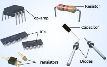
List of common semiconductor devices :
Description[edit]
Charge pumps use some form of switching device to control the connection of a supply voltage across a load through a capacitor. In a two stage cycle, in the first stage a capacitor is connected across the supply, charging it to that same voltage. In the second stage the circuit is reconfigured so that the capacitor is in series with the supply and the load. This doubles the voltage across the load - the sum of the original supply and the capacitor voltages. The pulsing nature of the higher voltage switched output is often smoothed by the use of an output capacitor.
An external or secondary circuit drives the switching, typically at tens of kilohertz up to several megahertz. The high frequency minimizes the amount of capacitance required, as less charge needs to be stored and dumped in a shorter cycle.
Charge pumps can double voltages, triple voltages, halve voltages, invert voltages, fractionally multiply or scale voltages (such as ×3/2, ×4/3, ×2/3, etc.) and generate arbitrary voltages by quickly alternating between modes, depending on the controller and circuit topology.
They are commonly used in low-power electronics (such as mobile phones) to raise and lower voltages for different parts of the circuitry - minimizing power consumption by controlling supply voltages carefully.
Terminology for PLL[edit]
The term charge pump is also commonly used in phase-locked loop (PLL) circuits even though there is no pumping action involved unlike in the circuit discussed above. A PLL charge pump is merely a bipolar switched current source. This means that it can output positive and negative current pulses into the loop filter of the PLL. It cannot produce higher or lower voltages than its power and ground supply levels.
Applications[edit]
- A common application for charge-pump circuits is in RS-232 level shifters, where they are used to derive positive and negative voltages (often +10 V and −10 V) from a single 5 V or 3 V power supply rail.
- Charge pumps can also be used as LCD or white-LED drivers, generating high bias voltages from a single low-voltage supply, such as a battery.
- Charge pumps are extensively used in NMOS memories and microprocessors to generate a negative voltage "VBB" (about −3 V), which is connected to the substrate. This guarantees that all N+-to-substrate junctions are reversely biased by 3 V or more, decreasing junction capacitance and increasing circuit speed.[1]
- A charge pump providing a negative voltage spike has been used in NES-compatible games not licensed by Nintendo in order to stun the Nintendo Entertainment System lockout chip.[2]
- As of 2007, charge pumps are integrated into nearly all EEPROM and flash-memory integrated circuits. These devices require a high-voltage pulse to "clean out" any existing data in a particular memory cell before it can be written with a new value. Early EEPROM and flash-memory devices required two power supplies: +5 V (for reading) and +12 V (for erasing). As of 2007, commercially available flash memory and EEPROM memory requires only one external power supply – generally 1.8 V or 3.3 V. A higher voltage, used to erase cells, is generated internally by an on-chip charge pump.
- Charge pumps are used in H bridges in high-side drivers for gate-driving high-side n-channel power MOSFETs and IGBTs. When the centre of a half bridge goes low, the capacitor is charged through a diode, and this charge is used to later drive the gate of the high-side FET a few volts above the source voltage so as to switch it on. This strategy works well, provided the bridge is regularly switched and avoids the complexity of having to run a separate power supply and permits the more efficient n-channel devices to be used for both switches. This circuit (requiring the periodic switching of the high-side FET) may also be called a "bootstrap" circuit, and some would differentiate between that and a charge pump (which would not require that switching).
wo-terminal devices:
- DIAC
- Diode (rectifier diode)
- Gunn diode
- IMPATT diode
- Laser diode
- Light-emitting diode (LED)
- Photocell
- Phototransistor
- PIN diode
- Schottky diode
- Solar cell
- Transient-voltage-suppression diode
- Tunnel diode
- VCSEL
- Zener diode
Three-terminal devices:
- Bipolar transistor
- Darlington transistor
- Field-effect transistor
- Insulated-gate bipolar transistor (IGBT)
- Silicon-controlled rectifier
- Thyristor
- TRIAC
- Unijunction transistor
Four-terminal devices:
- Hall effect sensor (magnetic field sensor)
- Photocoupler (Optocoupler)
Semiconductor device applications
All transistor types can be used as the building blocks of logic gates, which are fundamental in the design of digital circuits. In digital circuits like microprocessors, transistors act as on-off switches; in the MOSFET, for instance, the voltage applied to the gate determines whether the switch is on or off.
Transistors used for analog circuits do not act as on-off switches; rather, they respond to a continuous range of inputs with a continuous range of outputs. Common analog circuits include amplifiers and oscillators.
Circuits that interface or translate between digital circuits and analog circuits are known as mixed-signal circuits.
Power semiconductor devices are discrete devices or integrated circuits intended for high current or high voltage applications. Power integrated circuits combine IC technology with power semiconductor technology, these are sometimes referred to as "smart" power devices. Several companies specialize in manufacturing power semiconductors.
Improvements in transistor design[edit]
Shockley was upset about the device being credited to Brattain and Bardeen, who he felt had built it "behind his back" to take the glory. Matters became worse when Bell Labs lawyers found that some of Shockley's own writings on the transistor were close enough to those of an earlier 1925 patent by Julius Edgar Lilienfeld that they thought it best that his name be left off the patent application.
Shockley was incensed, and decided to demonstrate who was the real brains of the operation. A few months later he invented an entirely new, considerably more robust, type of transistor with a layer or 'sandwich' structure. This structure went on to be used for the vast majority of all transistors into the 1960s, and evolved into the bipolar junction transistor.
With the fragility problems solved, a remaining problem was purity. Making germanium of the required purity was proving to be a serious problem, and limited the yield of transistors that actually worked from a given batch of material. Germanium's sensitivity to temperature also limited its usefulness. Scientists theorized that silicon would be easier to fabricate, but few investigated this possibility. Gordon K. Teal was the first to develop a working silicon transistor, and his company, the nascent Texas Instruments, profited from its technological edge. From the late 1960s most transistors were silicon-based. Within a few years transistor-based products, most notably easily portable radios, were appearing on the market.
The static induction transistor, the first high frequency transistor,
A major improvement in manufacturing yield came when a chemist advised the companies fabricating semiconductors to use distilled rather than tap water: calcium ions present in tap water were the cause of the poor yields. "Zone melting", a technique using a band of molten material moving through the crystal, further increased crystal purity.

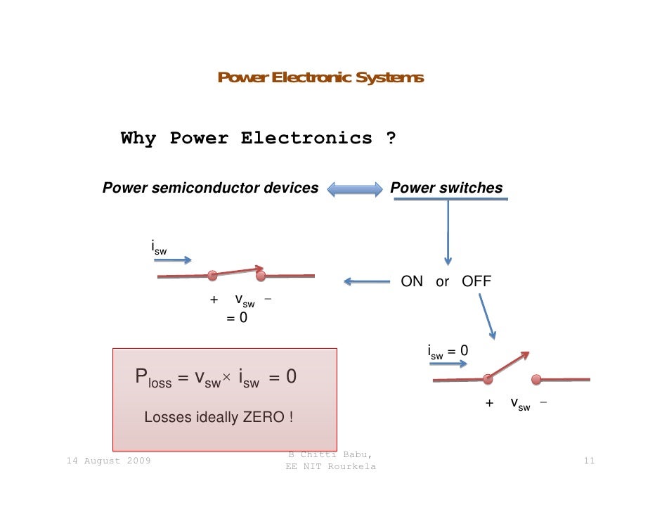
Why Semiconductor can act as electronic switch?
Semiconductor devices are made from n-type and p-type materials with ‘electrons’ and ‘holes’ serving as charge carriers. As others have said - the Gate or the Base can receive a voltage that controls the flow of current thru the device.
The Device can serve as an On/Off Switch or as an Amplifier that can increase the current more subtly than just on-off.
Switching characteristics in HARD AND SOFT Electron in Electronic circuit Probe +/_ :
- 1. SWITCHING CHARACTERISTICS OF POWER ELECTRONIC DEVICES
- 2. IDEAL SWITCH
- 3. PRACTICAL SWITCH
- 4. DIODE IDEAL PRACTICAL
- 5. TRANSISTOR INPUT OUTPUT
- 6. TRANSFER CHARACTERISTICS
- 7. TRANSISTOR SWITCHING TIME
- 8. SILICON CONTROLLED RECTIFIER
- 9. IDEAL CHARACTRISTICS OF SCR
- 10. SCR SWITCHING CHARACTERISTICS TURN ON
- 11. SCR SWITCHING CHARACTERISTICS TURN OFF
- 12. GATE CHARACTERISTICS
- 13. METAL OXIDE FIELD EFFECT TRANSISTOR
- 14. TURN ON CHARACTERISTICS
- 15. TURN OFF CHARACTERISTICS
- 16. INSULATED GATE BIPOLAR TRANSISTOR
- 17. DYNAMIC CHRACTERISTICS OF IGBT • TURN ON
- 18. TURN OFF CHARACTERISTICS
- 19. DIAC
- 20. TRIAC
- 21. UNIJUNCTION TRANSISTOR
- 22. PROGRAMMABLE UNIJUNCTION TRANSISTOR
- 23. GATE TURN OFF (IDEAL)
- 24. MOS CONTROLLED THYRISTORS
XXX . XXX May be Liquid light switch could enable more powerful electronics

Researchers have built a record energy-efficient switch, which uses the interplay of electricity and a liquid form of light, in semiconductor microchips. The device could form the foundation of future signal processing and information technologies, making electronics even more efficient.
Researchers have built a record energy-efficient switch, which uses the interplay of electricity and a liquid form of light, in semiconductor microchips. The device could form the foundation of future signal processing and information technologies, making electronics even more efficient.
Researchers have built a miniature electro - optical switch which can change the spin – or angular momentum – of a liquid form of light by applying electric fields to a semiconductor device a millionth of a metre in size. Their results, reported in the journal Nature Materials, demonstrate how to bridge the gap between light and electricity, which could enable the development of ever faster and smaller electronics.
There is a fundamental disparity between the way in which information is processed and transmitted by current technologies. To process information, electrical charges are moved around on semiconductor chips; and to transmit it, light flashes are sent down optical fibres. Current methods of converting between electrical and optical signals are both inefficient and slow, and researchers have been searching for ways to incorporate the two.
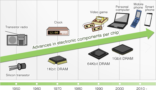
In order to make electronics faster and more powerful, more transistors need to be squeezed onto semiconductor chips. For the past 50 years, the number of transistors on a single chip has doubled every two years – this is known as Moore’s law. However, as chips keep getting smaller, scientists now have to deal with the quantum effects associated with individual atoms and electrons, and they are looking for alternatives to the electron as the primary carrier of information in order to keep up with Moore’s law and our thirst for faster, cheaper and more powerful electronics.
The A team have built a switch which utilizes a new state of matter called a Polariton Bose-Einstein condensate in order to mix electric and optical signals, while using miniscule amounts of energy.
Polarization Bose-Einstein condensates are generated by trapping light between mirrors spaced only a few millionths of a metre apart, and letting it interact with thin slabs of semiconductor material, creating a half-light, half-matter mixture known as a polarization.
Putting lots of polarizations in the same space can induce condensation – similar to the condensation of water droplets at high humidity – and the formation of a light-matter fluid which spins clockwise (spin-up) or anticlockwise (spin-down). By applying an electric field to this system, the researchers were able to control the spin of the condensate and switch it between up and down states. The polarization fluid emits light with clockwise or anticlockwise spin, which can be sent through optical fibres for communication, converting electrical to optical signals.
“The polarization switch unifies the best properties of electronics and optics into one tiny device that can deliver at very high speeds while using minimal amounts of power .
“We have made a field-effect light switch that can bridge the gap between optics and electronics, “ it have to reaching the limits of how small we can make transistors, and electronics based on liquid light could be a way of increasing the power and efficiency of the electronics we rely on.”
While the prototype device works at cryogenic temperatures, the researchers are developing other materials that can operate at room temperature, so that the device may be commercialized. The other key factor for the commercialization of the device is mass production and scalability. “Since this prototype is based on well-established fabrication technology, it has the potential to be scaled up in the near future,” .
The team is currently exploring options for commercializing the technology as well as integrating it with the existing technology base.
XXX . XXX 4%zero Allow difference between General switch and Transistor as a switch
A "general" switch is manually controlled; a transistor switch is electrically controlled. A general switch is a single component; a transistor switch requires supporting components (resistors, etc...). A general switch can have multiple positions (throws) and circuits (poles), but these have to be designed using transistor switches, using multiple transistors and supporting components.
A normal switch has only two positions although it may produce electrical bounce when switching from one state to the other. A transistor is perfectly capable of being at any position in between the two endpoint states, ie. it can function as something other than a switch.
In the electronics area, the big different is that the normal switch just using for manual control, it needs the human to press it, but the transistor switch can be using in the automatic control, you just give it a high or low voltage level, then the transistor switch will work for you, and the high or low voltage level can be output from the control circuit or a timer, or a comparator, this is what the normal switch can't do.
A mechanical switch provides essentially infinite OFF resistance and very low ON resistance. It also provides complete electrical isolation between the input control and output, such as a with a mechanical relay.
A transistor exhibits a finite leakage current when OFF and an ON resistance that can vary from a few tenths of an ohm to a few tens of milliohms depending upon its current rating and type of transistor (BJT or MOSFET). It also requires a common ground between the control input and the output.
A transistor exhibits a finite leakage current when OFF and an ON resistance that can vary from a few tenths of an ohm to a few tens of milliohms depending upon its current rating and type of transistor (BJT or MOSFET). It also requires a common ground between the control input and the output.
not forget that size matters. An everyday spst switch would not be practical on a small circuit board controlling mA. A transistor would not be practical for switching lights or motors due to higher current. So one size does not fit all .
Most mechanical switches latch. No action is needed once the switch is thrown. A transistor requires continuous control.
A manual pushbutton, for example, is a passive device. That is, it requires no electrical power to operate it. In addition, when the switch is in its "open" state, there is an "air gap" between the terminals of the switch.
A transistor, on the other hand, is an active device and requires power to operate it. There is no "open" state between the terminals, only a minimal conduction state.
A transistor, on the other hand, is an active device and requires power to operate it. There is no "open" state between the terminals, only a minimal conduction state.
so essentially manual or traditional switches are controlled both spacetime and time by living things like humans for example, whereas electronic switches or modern switches are controlled both space and time by discharged and discharged electrons while their life and death through electronic components of semiconductors (on or off through process components)
Wire Connection   old telephone exchange in New York City | Switch StoryLong long time ago, circuit connection is achieved using muscular means. The telephone network is one of a major communication system in the early days. To Call your buddy next block, the first step you have to do is to pick up the phone. A human operator will attend to your pick up. Speak to her about the intention to talk to your buddy. The operator will manually plunk in wire connector linking your home telephone to your buddy phone. And Yes, you can now talk to your friend because there are operator doing the switching at the end of your telephone line. Sounds a lot of manual work. Yes, this is the good old days. The telephone operators in the central telephone exchange house, are making the circuit connection manually. This is what this page is all about. All about switches. All about making a good short circuit. Not all short circuit is bad. In fact they are the fundamental building blocks in digital electronics. Many electronic design/interface are as simple as a switch.      |

Example of an electrical circuit using a relay
XXX . XXX 4%zero null 0 1 2 Switched capacitor
A switched capacitor is an electronic circuit element used for discrete-time signal processing. It works by moving charges into and out of capacitors when switches are opened and closed. Usually, non-overlapping signals are used to control the switches, so that not all switches are closed simultaneously. Filters implemented with these elements are termed "switched-capacitor filters", and depend only on the ratios between capacitances. This makes them much more suitable for use within integrated circuits, where accurately specified resistors and capacitors are not economical to construct.
The switched-capacitor resistor

The simplest switched-capacitor (SC) circuit is the switched-capacitor resistor, made of one capacitor C and two switches S1 and S2 which connect the capacitor with a given frequency alternately to the input and output of the SC. Each switching cycle transfers a charge from the input to the output at the switching frequency . The charge q on a capacitor C with a voltage V between the plates is given by:


where V is the voltage across the capacitor. Therefore, when S1 is closed while S2 is open, the charge stored in the capacitor CS is:

When S2 is closed, some of that charge is transferred out of the capacitor, after which the charge that remains in capacitor CS is:

Thus, the charge moved out of the capacitor to the output is:

Because this charge q is transferred at a rate f, the rate of transfer of charge per unit time is:

(A continuous transfer of charge from one node to another is equivalent to a current, so I (the symbol for electric current) is used.)
Substituting for q in the above, we have:

Let V be the voltage across the SC from input to output. So:

So the equivalent resistance R (i.e., the voltage–current relationship) is:

Thus, the SC behaves like a resistor whose value depends on capacitance CS and switching frequency f.
The SC resistor is used as a replacement for simple resistors in integrated circuits because it is easier to fabricate reliably with a wide range of values. It also has the benefit that its value can be adjusted by changing the switching frequency (i.e., it is a programmable resistance). See also: operational amplifier applications.
This same circuit can be used in discrete time systems (such as analog to digital converters) as a track and hold circuit. During the appropriate clock phase, the capacitor samples the analog voltage through switch one and in the second phase presents this held sampled value to an electronic circuit for processing.
The parasitic-sensitive integrator

Often switched-capacitor circuits are used to provide accurate voltage gain and integration by switching a sampled capacitor onto an op-amp with a capacitor in feedback. One of the earliest of these circuits is the parasitic-sensitive integrator developed by the Czech engineer Bedrich Hosticka.[2] Here is an analysis. Denote by the switching period. In capacitors,


Then, when S1 opens and S2 closes (they are never both closed at the same time), we have the following:
1) Because has just charged:


2) Because the feedback cap, , is suddenly charged with that much charge (by the op amp, which seeks a virtual short circuit between its inputs):

Now dividing 2) by :

And inserting 1):

This last equation represents what is going on in - it increases (or decreases) its voltage each cycle according to the charge that is being "pumped" from (due to the op-amp).
However, there is a more elegant way to formulate this fact if is very short. Let us introduce and and rewrite the last equation divided by dt:


Therefore, the op-amp output voltage takes the form:

This is an inverting integrator with an "equivalent resistance" . This allows its on-line or runtime adjustment (if we manage to make the switches oscillate according to some signal given by e.g. a microcontroller).

The parasitic insensitive integrator
Use in discrete-time systems
The delaying parasitic insensitive integrator has a wide use in discrete time electronic circuits such as biquad filters, anti-alias structures, and delta-sigma data converters. This circuit implements the following z-domain function:

The multiplying digital to analog converter

One useful characteristic of switched-capacitor circuits is that they can be used to perform many circuit tasks at the same time, which is difficult with non-discrete time components. The multiplying digital to analog converter (MDAC) is an example as it can take an analog input, add a digital value to it, and multiply this by some factor based on the capacitor ratios. The output of the MDAC is given by the following:


The MDAC is a common component in modern pipeline analog to digital converters as well as other precision analog electronics and was first created in the form above by Stephen Lewis and others at Bell Laboratories.[3]
Analysis of switched-capacitor circuits
Switched-capacitor circuits are analysed by writing down charge conservation equations, as in this article, and solving them with a computer algebra tool. For hand analysis and for getting more insight into the circuits, it is also possible to do a Signal-flow graph analysis, with a method that is very similar for switched-capacitor and continuous-time circuits
Aliasing
In signal processing and related disciplines, aliasing is an effect that causes different signals to become indistinguishable (or aliases of one another) when sampled. It also refers to the distortion or artifact that results when the signal reconstructed from samples is different from the original continuous signal.
Aliasing can occur in signals sampled in time, for instance digital audio, and is referred to as temporal aliasing. Aliasing can also occur in spatially sampled signals, for instance moiré patterns in digital images. Aliasing in spatially sampled signals is called spatial aliasing.
Aliasing is generally avoided by applying low pass filters- anti-aliasing filters to the analog signal before sampling.
Description

When a digital image is viewed, a reconstruction is performed by a display or printer device, and by the eyes and the brain. If the image data is processed in some ways during sampling or reconstruction, the reconstructed image will differ from the original image, and an alias is seen.
An example of spatial aliasing is the moiré pattern observed in a poorly pixelized image of a brick wall. Spatial anti-aliasing techniques avoid such poor pixelizations. Aliasing can be caused either by the sampling stage or the reconstruction stage; these may be distinguished by calling sampling aliasing prealiasing and reconstruction aliasing postaliasing.
Temporal aliasing is a major concern in the sampling of video and audio signals. Music, for instance, may contain high-frequency components that are inaudible to humans. If a piece of music is sampled at 32000 samples per second (Hz), any frequency components above 16000 Hz (the Nyquist frequency for this sampling rate) will cause aliasing when the music is reproduced by a digital to analog converter (DAC). To prevent this, an anti-aliasing filter is used to remove components above the Nyquist frequency prior to sampling.
In video or cinematography, temporal aliasing results from the limited frame rate, and causes the wagon-wheel effect, whereby a spoked wheel appears to rotate too slowly or even backwards. Aliasing has changed its apparent frequency of rotation. A reversal of direction can be described as a negative frequency. Temporal aliasing frequencies in video and cinematography are determined by the frame rate of the camera, but the relative intensity of the aliased frequencies is determined by the shutter timing (exposure time) or the use of a temporal aliasing reduction filter during filming.
Like the video camera, most sampling schemes are periodic; that is, they have a characteristic sampling frequency in time or in space. Digital cameras provide a certain number of samples (pixels) per degree or per radian, or samples per mm in the focal plane of the camera. Audio signals are sampled (digitized) with an analog-to-digital converter, which produces a constant number of samples per second. Some of the most dramatic and subtle examples of aliasing occur when the signal being sampled also has periodic content.
Bandlimited functions
Actual signals have a finite duration and their frequency content, as defined by the Fourier transform, has no upper bound. Some amount of aliasing always occurs when such functions are sampled. Functions whose frequency content is bounded (bandlimited) have an infinite duration in the time domain. If sampled at a high enough rate, determined by the bandwidth, the original function can, in theory, be perfectly reconstructed from the infinite set of samples.
Bandpass signals
Sometimes aliasing is used intentionally on signals with no low-frequency content, called bandpass signals. Undersampling, which creates low-frequency aliases, can produce the same result, with less effort, as frequency-shifting the signal to lower frequencies before sampling at the lower rate. Some digital channelizers[3] exploit aliasing in this way for computational efficiency. See Sampling (signal processing), Nyquist rate (relative to sampling), and Filter bank.
Sampling sinusoidal functions
Sinusoids are an important type of periodic function, because realistic signals are often modeled as the summation of many sinusoids of different frequencies and different amplitudes (for example, with a Fourier series or transform). Understanding what aliasing does to the individual sinusoids is useful in understanding what happens to their sum.

Here, a plot depicts a set of samples whose sample-interval is 1, and two (of many) different sinusoids that could have produced the samples. The sample-rate in this case is . For instance, if the interval is 1 second, the rate is 1 sample per second. Nine cycles of the red sinusoid and 1 cycle of the blue sinusoid span an interval of 10 samples. The corresponding number of cycles per sample are and . If these samples were produced by sampling functions and , they could also have been produced by the trigonometrically identical functions and which introduces the useful concept of negative frequency.


In general, when a sinusoid of frequency is sampled with frequency the resulting number of cycles per sample is (known as normalized frequency), and the samples are indistinguishable from those of another sinusoid (called an alias) whose normalized frequency differs from by any integer (positive or negative).[note 1] Replacing negative frequency sinusoids by their equivalent positive frequency representations, we can express all the aliases of frequency as for any integer with being the true value, and has units of cycles per sample. Then the alias of is (and vice versa).


Aliasing matters when one attempts to reconstruct the original waveform from its samples. The most common reconstruction technique produces the smallest of the frequencies. So it is usually important that be the unique minimum. A necessary and sufficient condition for that is where is commonly called the Nyquist frequency of a system that samples at rate In our example, the Nyquist condition is satisfied if the original signal is the blue sinusoid (). But if the usual reconstruction method will produce the blue sinusoid instead of the red one.


Folding
In the example above, and are symmetrical around the frequency And in general, as increases from 0 to decreases from to Similarly, as increases from to continues decreasing from to 0.


A graph of amplitude vs frequency for a single sinusoid at frequency and some of its aliases at and would look like the 4 black dots in the first figure below. The red lines depict the paths (loci) of the 4 dots if we were to adjust the frequency and amplitude of the sinusoid along the solid red segment (between and ). No matter what function we choose to change the amplitude vs frequency, the graph will exhibit symmetry between 0 and This symmetry is commonly referred to as folding, and another name for (the Nyquist frequency) is folding frequency. Folding is often observed in practice when viewing the frequency spectrum of real-valued samples, such as the second figure below.


Complex sinusoids
Complex sinusoids are waveforms whose samples are complex numbers, and the concept of negative frequency is necessary to distinguish them. In that case, the frequencies of the aliases are given by just: Therefore, as increases from to goes from up to 0. Consequently, complex sinusoids do not exhibit folding. Complex samples of real-valued sinusoids have zero-valued imaginary parts and do exhibit folding.


Sample frequency

When the condition is met for the highest frequency component of the original signal, then it is met for all the frequency components, a condition called the Nyquist criterion. That is typically approximated by filtering the original signal to attenuate high frequency components before it is sampled. These attenuated high frequency components still generate low-frequency aliases, but typically at low enough amplitudes that they do not cause problems. A filter chosen in anticipation of a certain sample frequency is called an anti-aliasing filter.

The filtered signal can subsequently be reconstructed, by interpolation algorithms, without significant additional distortion. Most sampled signals are not simply stored and reconstructed. But the fidelity of a theoretical reconstruction (via the Whittaker–Shannon interpolation formula) is a customary measure of the effectiveness of sampling.
Flash Back usage
Historically the term aliasing evolved from radio engineering because of the action of superheterodyne receivers. When the receiver shifts multiple signals down to lower frequencies, from RF to IF by heterodyning, an unwanted signal, from an RF frequency equally far from the local oscillator (LO) frequency as the desired signal, but on the wrong side of the LO, can end up at the same IF frequency as the wanted one. If it is strong enough it can interfere with reception of the desired signal. This unwanted signal is known as an image or alias of the desired signal.
Angular aliasing
Aliasing occurs whenever the use of discrete elements to capture or produce a continuous signal causes frequency ambiguity.
Spatial aliasing, particular of angular frequency, can occur when reproducing a light field[4] or sound field with discrete elements, as in 3D displays or wave field synthesis of sound.
This aliasing is visible in images such as posters with lenticular printing: if they have low angular resolution, then as one moves past them, say from left-to-right, the 2D image does not initially change (so it appears to move left), then as one moves to the next angular image, the image suddenly changes (so it jumps right) – and the frequency and amplitude of this side-to-side movement corresponds to the angular resolution of the image (and, for frequency, the speed of the viewer's lateral movement), which is the angular aliasing of the 4D light field.
The lack of parallax on viewer movement in 2D images and in 3-D film produced by stereoscopic glasses (in 3D films the effect is called "yawing", as the image appears to rotate on its axis) can similarly be seen as loss of angular resolution, all angular frequencies being aliased to 0 (constant).
More examples
Online audio example
The qualitative effects of aliasing can be heard in the following audio demonstration. Six saw tooth waves are played in succession, with the first two sawtooths having a fundamental frequency of 440 Hz (A4), the second two having fundamental frequency of 880 Hz (A5), and the final two at 1760 Hz (A6). The saw tooths alternate between bandlimited (non-aliased) saw tooths and aliased saw tooths and the sampling rate is 22.05 kHz. The band limited saw tooths are synthesized from the saw tooth waveform's Fourier series such that no harmonics above the Nyquist frequency are present.
The aliasing distortion in the lower frequencies is increasingly obvious with higher fundamental frequencies, and while the band limited sawtooth is still clear at 1760 Hz, the aliased saw tooth is degraded and harsh with a buzzing audible at frequencies lower than the fundamental.
Direction finding
A form of spatial aliasing can also occur in antenna arrays or microphone arrays used to estimate the direction of arrival of a wave signal, as in geophysical exploration by seismic waves. Waves must be sampled at more than two points per wavelength, or the wave arrival direction becomes ambiguous.
XXX . XXX 4%zero null 0 1 2 3 4 Charge pump
A charge pump is a kind of DC to DC converter that uses capacitors for energetic charge storage to raise or lower voltage. Charge-pump circuits are capable of high efficiencies, sometimes as high as 90–94 %, while being electrically simple circuits.

Description
Charge pumps use some form of switching device to control the connection of a supply voltage across a load through a capacitor. In a two stage cycle, in the first stage a capacitor is connected across the supply, charging it to that same voltage. In the second stage the circuit is reconfigured so that the capacitor is in series with the supply and the load. This doubles the voltage across the load - the sum of the original supply and the capacitor voltages. The pulsing nature of the higher voltage switched output is often smoothed by the use of an output capacitor.
An external or secondary circuit drives the switching, typically at tens of kilohertz up to several megahertz. The high frequency minimizes the amount of capacitance required, as less charge needs to be stored and dumped in a shorter cycle.
Charge pumps can double voltages, triple voltages, halve voltages, invert voltages, fractionally multiply or scale voltages (such as ×3/2, ×4/3, ×2/3, etc.) and generate arbitrary voltages by quickly alternating between modes, depending on the controller and circuit topology.
They are commonly used in low-power electronics (such as mobile phones) to raise and lower voltages for different parts of the circuitry - minimizing power consumption by controlling supply voltages carefully.
Terminology for PLL
The term charge pump is also commonly used in phase-locked loop (PLL) circuits even though there is no pumping action involved unlike in the circuit discussed above. A PLL charge pump is merely a bipolar switched current source. This means that it can output positive and negative current pulses into the loop filter of the PLL. It cannot produce higher or lower voltages than its power and ground supply levels.
Applications
- A common application for charge-pump circuits is in RS-232 level shifters, where they are used to derive positive and negative voltages (often +10 V and −10 V) from a single 5 V or 3 V power supply rail.
- Charge pumps can also be used as LCD or white-LED drivers, generating high bias voltages from a single low-voltage supply, such as a battery.
- Charge pumps are extensively used in NMOS memories and microprocessors to generate a negative voltage "VBB" (about −3 V), which is connected to the substrate. This guarantees that all N+-to-substrate junctions are reversely biased by 3 V or more, decreasing junction capacitance and increasing circuit speed.[1]
- A charge pump providing a negative voltage spike has been used in NES-compatible games not licensed by Nintendo in order to stun the Nintendo Entertainment System lockout chip.[2]
- As of 2007, charge pumps are integrated into nearly all EEPROM and flash-memory integrated circuits. These devices require a high-voltage pulse to "clean out" any existing data in a particular memory cell before it can be written with a new value. Early EEPROM and flash-memory devices required two power supplies: +5 V (for reading) and +12 V (for erasing). As of 2007, commercially available flash memory and EEPROM memory requires only one external power supply – generally 1.8 V or 3.3 V. A higher voltage, used to erase cells, is generated internally by an on-chip charge pump.
- Charge pumps are used in H bridges in high-side drivers for gate-driving high-side n-channel power MOSFETs and IGBTs. When the centre of a half bridge goes low, the capacitor is charged through a diode, and this charge is used to later drive the gate of the high-side FET a few volts above the source voltage so as to switch it on. This strategy works well, provided the bridge is regularly switched and avoids the complexity of having to run a separate power supply and permits the more efficient n-channel devices to be used for both switches. This circuit (requiring the periodic switching of the high-side FET) may also be called a "bootstrap" circuit, and some would differentiate between that and a charge pump (which would not require that switching).


Dickson charge pump with diodes
 PLL charge pump
A charge transfer switch OR CTS charge pump is a charge pump that offers better low-voltage performance and "a better voltage pumping gain and a higher output voltage" than previous charge pumps such as the Dickson charge pump.
Thyristor switched capacitor is defined as 'a shunt-connected, thyristor-switched capacitor whose effective reactance is varied in a stepwise manner by full- or zero- conduction operation of the thyristor valve'.
Principles of operation
The principle of the TSC is shown in Figures 6.12 and 6.13. The susceptance is adjusted by controlling the number of parallel capacitors in conduction. Each capacitor always conducts for an integral number of half-cycles. With k capacitors in parallel, each controlled by a switch as in Figure 6.13, the total susceptance can be equal to that of any combination of the k individual susceptances taken 0, 1, 2 . . . . or k at a time. The total susceptance thus varies in a stepwise manner. In principle the steps can be made as small and as numerous as desired, by having a sufficient number of individually switched capacitors. For a given number k the maximum number of steps will be obtained when no two combinations are equal, which requires at least that all the individual susceptances be different. This degree of flexibility is not usually sought in power-system compensators because of the consequent complexity of the controls, and because it is generally more economic to make most of the susceptances equal. One compromise is the so-called binary system in which there are (k - 1) equal susceptances B and one susceptance B/2. The half-susceptance increases the number of combinations from k to 2k.
The relation between the compensator current and the number of capacitors conducting is shown in Figure 6.14 (for constant terminal voltage). Ignoring switching transients, the current is sinusoidal, that is, it contains no harmonics.

Fig. 6.12 Alternative arangements of three-phase thyristor-switchet capacitor. (a) delta-connected secondary, Delta-connected TSC; ant (b) wye-connected secondary, wye-connected TSC (four-wire system).

Fig. 6.12 Principles of operation of TSC. Each phase of Figure 6.12 comprises of parallel combinations of switched capacitors of this type.

Fig. 6.14 Relationship between current and number of capacitors conducting in the TSC.
previous The thyristor-controlled transformer (TCT) .
 Roll Film Capacitor Electrolyte
++++++++++++++++++++++++++++++++++++++++++++++++++++++++++++
SWITCH ( Short Wave Interaction To Couple Highway )
BELIEVABLE OF PROCESSING COMPONENT
ON ELECTRONIC CIRCUIT SWITCHING

++++++++++++++++++++++++++++++++++++++++++++++++++++++++++++
Tidak ada komentar:
Posting Komentar