
In the design and design of the engineering component and electronic system equipment in the 21st century and research and development in the 22nd century is based on the design of analog and digital systems that are processed by component components which we call IC (integrated circuit) and CHIP which consists of many IC layers. the ADA process for the benefit of MARIA PREFER is very important because it is a very modern energy bridge for energy efficiency and effectiveness when we need electronic equipment for an independent system with very very efficient energy requirements which may only require currents in nano amperes and pico amperes especially our needs for the 22nd century our journey to other planets and even to the nearest star is not impossible, so we need a small energy transfer with optimum output for enough travel to consume in the speed of light (E = MC2 by having ROS = Robot Operating System C2TAM). the electronic process that we know of in the 21st century is an electronic process consisting of binary numbers that has to do with electronic switches and signal conditioning circuits connected to analog, digital, optical sensor and transducer replacement circuits. So the process is ADC, which is from human numbers to electronic binaries (switches, sensors and signal conditioning) called electronic process transfers (in nano seconds and picoseconds) and then becomes DAC electronic process transfers, from digital binary numbers to human languages, namely alphabets or numbers where represented by the Transducer into modern electronic output components such as touchscreens and motion sensors.
LOVE ON MARIA PREFER

( Gen. Mac Tech Zone light speed motion in e- STAR C )
Design UTC in e- S H I N to A/ D / S Tour Route
UTCs are used as sensing units, data processing or storage unit, driving or output unit, and power or energy management units. Ultra-thin chips ( UTC ) .
__________________________________________________________________________________________________
ADC (Analog To Digital Converter)
Digital Electronics | Analog to digital conversion
Digital Signal: A digital signal is a signal that represents data as a sequence of discrete values; at any given time it can only take on one of a finite number of values.
Analog Signal: An analog signal is any continuous signal for which the time varying feature of the signal is a representation of some other time varying quantity i.e., analogous to another time varying signal.
The following techniques can be used for Analog to Digital Conversion:
a. PULSE CODE MODULATION:
The most common technique to change an analog signal to digital data is called pulse code modulation (PCM). A PCM encoder has the following three processes:- Sampling
- Quantization
- Encoding
The low pass filter eliminates the high frequency components present in the input analog signal to ensure that the input signal to sampler is free from the unwanted frequency components.This is done to avoid aliasing of the message signal.
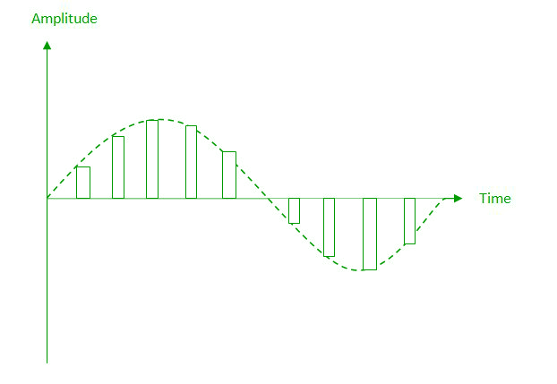
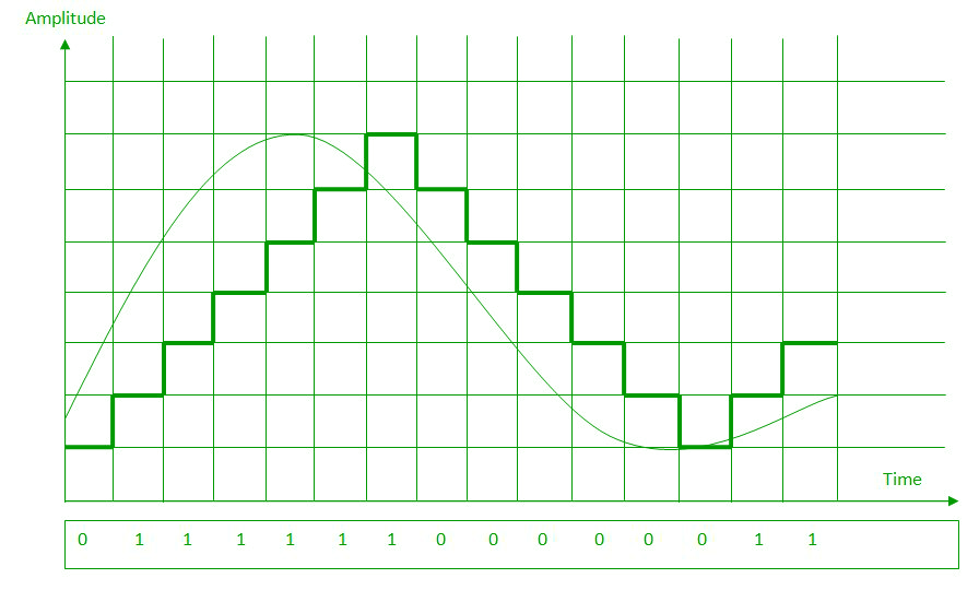
- Sampling – The first step in PCM is sampling.
Sampling is a process of measuring the amplitude of a continuous-time
signal at discrete instants, converting the continuous signal into a
discrete signal. There are three sampling methods:
(i) Ideal Sampling: In ideal Sampling also known as
Instantaneous sampling pulses from the analog signal are sampled. This
is an ideal sampling method and cannot be easily implemented.
(ii) Natural Sampling: Natural Sampling is a practical method of sampling in which pulse have finite width equal to T.The result is a sequence of samples that retain the shape of the analog signal.
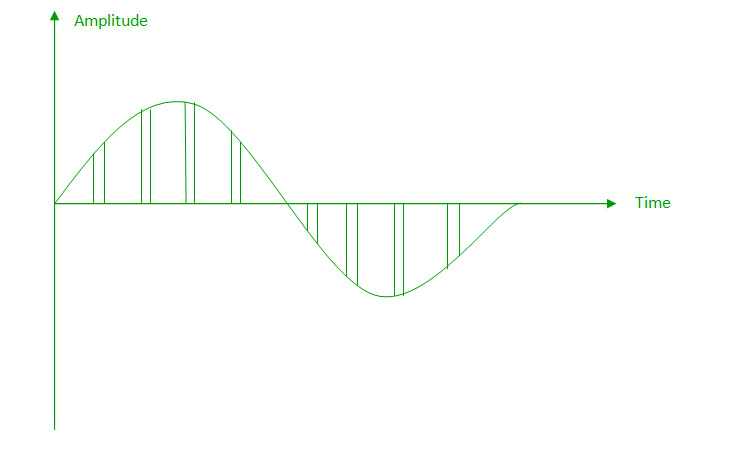
(iii) Flat top sampling: In comparison to natural sampling flat top sampling can be easily obtained. In this sampling technique, the top of the samples remains constant by using a circuit. This is the most common sampling method used.
Nyquist Theorem:
One important consideration is the sampling rate or frequency. According to the Nyquist theorem, the sampling rate must be at least 2 times the highest frequency contained in the signal. It is also known as the minimum sampling rate and given by:
Fs =2*fh - Quantization –
The result of sampling is a series of pulses with amplitude values between the maximum and minimum amplitudes of the signal. The set of amplitudes can be infinite with non-integral values between two limits. The following are the steps in Quantization:
- We assume that the signal has amplitudes between Vmax and Vmin
- We divide it into L zones each of height d where,
d= (Vmax- Vmin)/ L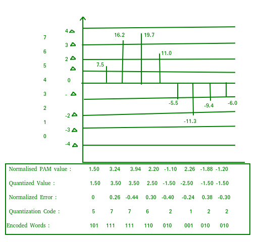
- The value at the top of each sample in the graph shows the actual amplitude.
- The normalized pulse amplitude modulation(PAM) value is calculated using the formula amplitude/d.
- After this we calculate the quantized value which the process selects from the middle of each zone.
- The Quantized error is given by the difference between quantised value and normalised PAM value.
- The Quantization code for each sample based on quantization levels at the left of the graph.
- Encoding –
The digitization of the analog signal is done by the encoder. After each sample is quantized and the number of bits per sample is decided, each sample can be changed to an n bit code. Encoding also minimizes the bandwidth used.
b. DELTA MODULATION :
Since PCM is a very complex technique, other techniques have been developed to reduce the complexity of PCM. The simplest is delta Modulation. Delta Modulation finds the change from the previous value.Modulator – The modulator is used at the sender site to create a stream of bits from an analog signal. The process records a small positive change called delta. If the delta is positive, the process records a 1 else the process records a 0. The modulator builds a second signal that resembles a staircase. The input signal is then compared with this gradually made staircase signal.
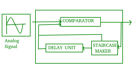
We have the following rules for output:
- If the input analog signal is higher than the last value of the staircase signal, increase delta by 1, and the bit in the digital data is 1.
- If the input analog signal is lower than the last value of the staircase signal, decrease delta by 1, and the bit in the digital data is 0.
c. ADAPTIVE DELTA MODULATION:
The performance of a delta modulator can be improved significantly by making the step size of the modulator assume a time-varying form. A larger step-size is needed where the message has a steep slope of modulating signal and a smaller step-size is needed where the message has a small slope. The size is adapted according to the level of the input signal. This method is known as adaptive delta modulation (ADM).
___________________________________________________________________________________________________
Digital Electronics | Digital to Analog Conversion
Digital Signal – A digital signal is a signal that represents data as a sequence of discrete values; at any given time it can only take on one of a finite number of values.
Analog Signal – An analog signal is any continuous signal for which the time varying feature of the signal is a representation of some other time varying quantity i.e., analogous to another time varying signal.
The following techniques can be used for Digital to Analog Conversion:
1. Amplitude Shift keying – Amplitude Shift Keying is a technique in which carrier signal is analog and data to be modulated is digital. The amplitude of analog carrier signal is modified to reflect binary data.
The binary signal when modulated gives a zero value when the binary data represents 0 while gives the carrier output when data is 1. The frequency and phase of the carrier signal remain constant.

Advantages of amplitude shift Keying –
- It can be used to transmit digital data over optical fiber.
- The receiver and transmitter have a simple design which also makes it comparatively inexpensive.
- It uses lesser bandwidth as compared to FSK thus it offers high bandwidth efficiency.
- It is susceptible to noise interference and entire transmissions could be lost due to this.
- It has lower power efficiency.
The output of a frequency shift keying modulated wave is high in frequency for a binary high input and is low in frequency for a binary low input. The amplitude and phase of the carrier signal remain constant.

Advantages of frequency shift Keying –
- Frequency shift keying modulated signal can help avoid the noise problems beset by ASK.
- It has lower chances of an error.
- It provides high signal to noise ratio.
- The transmitter and receiver implementations are simple for low data rate application.
- It uses larger bandwidth as compared to ASK thus it offers less bandwidth efficiency.
- It has lower power efficiency.

It is further categorized as follows:
- Binary Phase Shift Keying (BPSK):
BPSK also known as phase reversal keying or 2PSK is the simplest form of phase shift keying. The Phase of the carrier wave is changed according to the two binary inputs. In Binary Phase shift keying, difference of 180 phase shift is used between binary 1 and binary 0. This is regarded as the most robust digital modulation technique and is used for long distance wireless communication.
- Quadrature phase shift keying:
This technique is used to increase the bit rate i.e we can code two bits onto one single element. It uses four phases to encode two bits per symbol. QPSK uses phase shifts of multiples of 90 degrees. It has double data rate carrying capacity compare to BPSK as two bits are mapped on each constellation points.
- It is a more power efficient modulation technique as compared to ASK and FSK.
- It has lower chances of an error.
- It allows data to be carried along a communication signal much more efficiently as compared to FSK.
- It offers low bandwidth efficiency.
- The detection and recovery algorithms of binary data is very complex.
- It is a non coherent reference signal.
Digital-to-analog converter
In electronics, a digital-to-analog converter (DAC, D/A, D2A, or D-to-A) is a system that converts a digital signal into an analog signal. An analog-to-digital converter (ADC) performs the reverse function.
There are several DAC architectures; the suitability of a DAC for a particular application is determined by figures of merit including: resolution, maximum sampling frequency and others. Digital-to-analog conversion can degrade a signal, so a DAC should be specified that has insignificant errors in terms of the application.
DACs are commonly used in music players to convert digital data streams into analog audio signals. They are also used in televisions and mobile phones to convert digital video data into analog video signals which connect to the screen drivers to display monochrome or color images. These two applications use DACs at opposite ends of the frequency/resolution trade-off. The audio DAC is a low-frequency, high-resolution type while the video DAC is a high-frequency low- to medium-resolution type.
Due to the complexity and the need for precisely matched components, all but the most specialized DACs are implemented as integrated circuits (ICs). Discrete DACs would typically be extremely high speed low resolution power hungry types, as used in military radar systems. Very high speed test equipment, especially sampling oscilloscopes, may also use discrete DACs.

8-channel Cirrus Logic CS4382 digital-to-analog converter as used in a sound card.
Overview

Ideally sampled signal.

Piecewise constant output of a conventional DAC lacking a reconstruction filter. In a practical DAC, a filter or the finite bandwidth of the device smooths out the step response into a continuous curve.
An ideal DAC converts the abstract numbers into a conceptual sequence of impulses that are then processed by a reconstruction filter using some form of interpolation to fill in data between the impulses. A conventional practical DAC converts the numbers into a piecewise constant function made up of a sequence of rectangular functions that is modeled with the zero-order hold. Other DAC methods (such as those based on delta-sigma modulation) produce a pulse-density modulated output that can be similarly filtered to produce a smoothly varying signal.
As per the Nyquist–Shannon sampling theorem, a DAC can reconstruct the original signal from the sampled data provided that its bandwidth meets certain requirements (e.g., a baseband signal with bandwidth less than the Nyquist frequency). Digital sampling introduces quantization error that manifests as low-level noise in the reconstructed signal.
Applications

A simplified functional diagram of an 8-bit DAC
Audio

Top-loading CD player and external digital-to-analog converter.
Specialist standalone DACs can also be found in high-end hi-fi systems. These normally take the digital output of a compatible CD player or dedicated transport (which is basically a CD player with no internal DAC) and convert the signal into an analog line-level output that can then be fed into an amplifier to drive speakers.
Similar digital-to-analog converters can be found in digital speakers such as USB speakers, and in sound cards.
In voice over IP applications, the source must first be digitized for transmission, so it undergoes conversion via an ADC, and is then reconstructed into analog using a DAC on the receiving party's end.
Video
Video sampling tends to work on a completely different scale altogether thanks to the highly nonlinear response both of cathode ray tubes (for which the vast majority of digital video foundation work was targeted) and the human eye, using a "gamma curve" to provide an appearance of evenly distributed brightness steps across the display's full dynamic range - hence the need to use RAMDACs in computer video applications with deep enough colour resolution to make engineering a hardcoded value into the DAC for each output level of each channel impractical (e.g. an Atari ST or Sega Genesis would require 24 such values; a 24-bit video card would need 768...). Given this inherent distortion, it is not unusual for a television or video projector to truthfully claim a linear contrast ratio (difference between darkest and brightest output levels) of 1000:1 or greater, equivalent to 10 bits of audio precision even though it may only accept signals with 8-bit precision and use an LCD panel that only represents 6 or 7 bits per channel.Video signals from a digital source, such as a computer, must be converted to analog form if they are to be displayed on an analog monitor. As of 2007, analog inputs were more commonly used than digital, but this changed as flat panel displays with DVI and/or HDMI connections became more widespread.[citation needed] A video DAC is, however, incorporated in any digital video player with analog outputs. The DAC is usually integrated with some memory (RAM), which contains conversion tables for gamma correction, contrast and brightness, to make a device called a RAMDAC.
A device that is distantly related to the DAC is the digitally controlled potentiometer, used to control an analog signal digitally.
Mechanical

IBM Selectric typewriter uses a mechanical digital-to-analog converter to control its typeball.
Types
The most common types of electronic DACs are- The pulse-width modulator where a stable current or voltage is switched into a low-pass analog filter with a duration determined by the digital input code. This technique is often used for electric motor speed control and dimming LED lamps.
- Oversampling DACs or interpolating DACs such as those employing delta-sigma modulation, use a pulse density conversion technique with oversampling. Speeds of greater than 100 thousand samples per second (for example, 192 kHz) and resolutions of 24 bits are attainable with delta-sigma DACs.
- The binary-weighted DAC, which contains individual electrical
components for each bit of the DAC connected to a summing point,
typically an operational amplifier. Each input in the summing has powers-of-two values with most current or voltage at the most-significant bit.
These precise voltages or currents sum to the correct output value.
This is one of the fastest conversion methods but suffers from poor
accuracy because of the high precision required for each individual
voltage or current. This type of converter is usually limited to 8-bit resolution or less.[citation needed]
- Switched resistor DAC contains a parallel resistor network. Individual resistors are enabled or bypassed in the network based on the digital input.
- Switched current source DAC, from which different current sources are selected based on the digital input.
- Switched capacitor DAC contains a parallel capacitor network. Individual capacitors are connected or disconnected with switches based on the input.
- The R-2R ladder DAC which is a binary-weighted DAC that uses a repeating cascaded structure of resistor values R and 2R. This improves the precision due to the relative ease of producing equal valued-matched resistors.
- The successive approximation or cyclic DAC, which successively constructs the output during each cycle. Individual bits of the digital input are processed each cycle until the entire input is accounted for.
- The thermometer-coded DAC, which contains an equal resistor or current-source segment for each possible value of DAC output. An 8-bit thermometer DAC would have 255 segments, and a 16-bit thermometer DAC would have 65,535 segments. This is a fast and highest precision DAC architecture but at the expense of requiring many components which, for practical implementations, fabrication requires high-density IC processes.
- Hybrid DACs, which use a combination of the above techniques in a
single converter. Most DAC integrated circuits are of this type due to
the difficulty of getting low cost, high speed and high precision in one
device.
- The segmented DAC, which combines the thermometer-coded principle for the most significant bits and the binary-weighted principle for the least significant bits. In this way, a compromise is obtained between precision (by the use of the thermometer-coded principle) and number of resistors or current sources (by the use of the binary-weighted principle). The full binary-weighted design means 0% segmentation, the full thermometer-coded design means 100% segmentation.
- Most DACs shown in this list rely on a constant reference voltage or current to create their output value. Alternatively, a multiplying DAC takes a variable input voltage or current as a conversion reference. This puts additional design constraints on the bandwidth of the conversion circuit.
Performance
The most important characteristics of a DAC are:- Resolution
- The number of possible output levels the DAC is designed to reproduce. This is usually stated as the number of bits it uses, which is the binary logarithm of the number of levels. For instance a 1-bit DAC is designed to reproduce 2 (21) levels while an 8-bit DAC is designed for 256 (28) levels. Resolution is related to the effective number of bits which is a measurement of the actual resolution attained by the DAC. Resolution determines color depth in video applications and audio bit depth in audio applications.
- Maximum sampling rate
- The maximum speed at which the DACs circuitry can operate and still produce correct output. The Nyquist–Shannon sampling theorem defines a relationship between this and the bandwidth of the sampled signal.
- Monotonicity
- The ability of a DAC's analog output to move only in the direction that the digital input moves (i.e., if the input increases, the output doesn't dip before asserting the correct output.) This characteristic is very important for DACs used as a low frequency signal source or as a digitally programmable trim element.[citation needed]
- Total harmonic distortion and noise (THD+N)
- A measurement of the distortion and noise introduced to the signal by the DAC. It is expressed as a percentage of the total power of unwanted harmonic distortion and noise that accompany the desired signal.
- Dynamic range
- A measurement of the difference between the largest and smallest signals the DAC can reproduce expressed in decibels. This is usually related to resolution and noise floor.
Non-linear PCM encodings (A-law / μ-law, ADPCM, NICAM) attempt to improve their effective dynamic ranges by using logarithmic step sizes between the output signal strengths represented by each data bit. This trades greater quantisation distortion of loud signals for better performance of quiet signals.
Figures of merit
- Static performance:
- Differential nonlinearity (DNL) shows how much two adjacent code analog values deviate from the ideal 1 LSB step.
- Integral nonlinearity (INL) shows how much the DAC transfer characteristic deviates from an ideal one. That is, the ideal characteristic is usually a straight line; INL shows how much the actual voltage at a given code value differs from that line, in LSBs (1 LSB steps).
- Gain
- Offset
- Noise is ultimately limited by the thermal noise generated by passive components such as resistors. For audio applications and in room temperatures, such noise is usually a little less than 1 μV (microvolt) of white noise. This limits performance to less than 20~21 bits even in 24-bit DACs.
- Frequency domain performance
- Spurious-free dynamic range (SFDR) indicates in dB the ratio between the powers of the converted main signal and the greatest undesired spur.
- Signal-to-noise and distortion ratio (SNDR) indicates in dB the ratio between the powers of the converted main signal and the sum of the noise and the generated harmonic spurs
- i-th harmonic distortion (HDi) indicates the power of the i-th harmonic of the converted main signal
- Total harmonic distortion (THD) is the sum of the powers of all HDi
- If the maximum DNL error is less than 1 LSB, then the D/A converter is guaranteed to be monotonic. However, many monotonic converters may have a maximum DNL greater than 1 LSB.
- Time domain performance:
- Glitch impulse area (glitch energy)
- Response uncertainty
- Time nonlinearity (TNL)
Digital Electronics and Computer Organization
Digital Electronics
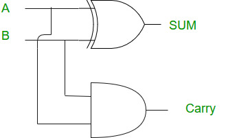
Half Adder

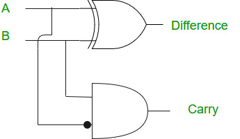
Half Subtractor

K-Map
In many digital circuits and practical problems we need to find expression with minimum variables. We can minimize Boolean expressions of 3, 4 variables very easily using K-map without using any Boolean algebra theorems. K-map can take two forms Sum of Product (SOP) and Product of Sum (POS) according to the need of problem. K-map is table like representation but it gives more information than TRUTH TABLE. We fill grid of K-map with 0’s and 1’s then solve it by making groups.
Steps to solve expression using K-map-
- Select K-map according to the number of variables.
- Identify minterms or maxterms as given in problem.
- For SOP put 1’s in blocks of K-map respective to the minterms (0’s elsewhere).
- For POS put 0’s in blocks of K-map respective to the maxterms(1’s elsewhere).
- Make rectangular groups containing total terms in power of two like 2,4,8 ..(except 1) and try to cover as many elements as you can in one group.
- From the groups made in step 5 find the product terms and sum them up for SOP form.
SOP FORM
- K-map of 3 variables-

A’C
From green group we get product term—
AB
Summing these product terms we get- Final expression (A’C+AB)
- K-map for 4 variables

QS
From green group we get product term—
Q’S’
Summing these product terms we get- Final expression (QS+Q’S’)
POS FORM
- K-map of 3 variables-

From red group we find terms
A B C’
Taking complement of these two
A’ B’ C
Now sum up them
(A’ + B’ + C)
From green group we find terms
B C
Taking complement of these two terms
B’ C’
Now sum up them
(B’+C’)
From brown group we find terms
A’ B’ C’
Taking complement of these two
A B C
Now sum up them
(A + B + C)
We will take product of these three terms :Final expression (A’ + B’ + C) (B’ + C’) (A + B + C)
2. K-map of 4 variables-
F(A,B,C,D)=π(3,5,7,8,10,11,12,13)

From green group we find terms
C’ D B
Taking their complement and summing them
(C+D’+B’)
From red group we find terms
C D A’
Taking their complement and summing them
(C’+D’+A)
From blue group we find terms
A C’ D’
Taking their complement and summing them
(A’+C+D)
From brown group we find terms
A B’ C
Taking their complement and summing them
(A’+B+C’)
Finally we express these as product –(C+D’+B’).(C’+D’+A).(A’+C+D).(A’+B+C’)
PITFALL– *Always remember POS ≠ (SOP)’
*The correct form is (POS of F)=(SOP of F’)’
Counters
in digital logic and computing, a Counter is a device which stores (and sometimes displays) the number of times a particular event or process has occurred, often in relationship to a clock signal. Counters are used in digital electronics for counting purpose, they can count specific event happening in the circuit. For example, in UP counter a counter increases count for every rising edge of clock. Not only counting, a counter can follow the certain sequence based on our design like any random sequence 0,1,3,2… .They can also be designed with the help of flip flops.
Counter Classification
Counters are broadly divided into two categories- Asynchronous counter
- Synchronous counter
In asynchronous counter we don’t use universal clock, only first flip flop is driven by main clock and the clock input of rest of the following counters is driven by output of previous flip flops. We can understand it by following diagram-
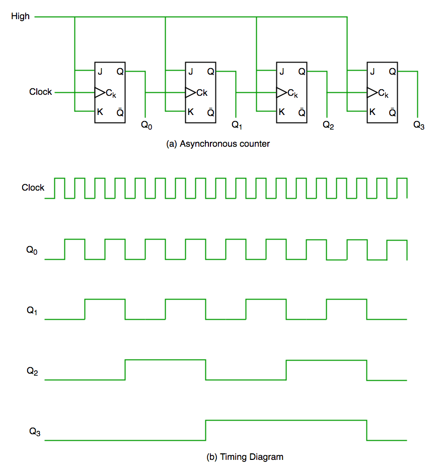
It is evident from timing diagram that Q0 is changing as soon as the rising edge of clock pulse is encountered, Q1 is changing when rising edge of Q0 is encountered(because Q0 is like clock pulse for second flip flop) and so on. In this way ripples are generated through Q0,Q1,Q2,Q3 hence it is also called RIPPLE counter.
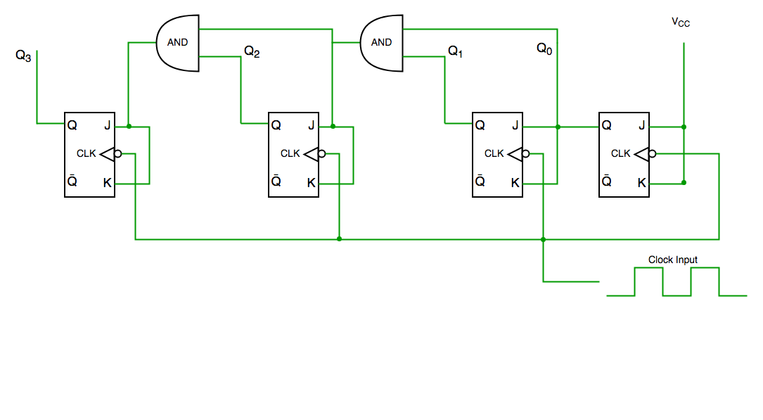
2. Synchronous Counter
Unlike the asynchronous counter, synchronous counter has one global clock which drives each flip flop so output changes in parallel. The one advantage of synchronous counter over asynchronous counter is, it can operate on higher frequency than asynchronous counter as it does not have cumulative delay because of same clock is given to each flip flop.
Synchronous counter circuit

Timing diagram synchronous counter
From circuit diagram we see that Q0 bit gives response to each
falling edge of clock while Q1 is dependent on Q0, Q2 is dependent on Q1
and Q0 , Q3 is dependent on Q2,Q1 and Q0.
Decade Counter
A decade counter counts ten different states and then reset to its
initial states. A simple decade counter will count from 0 to 9 but we
can also make the decade counters which can go through any ten states
between 0 to 15(for 4 bit counter).| Clock pulse | Q3 | Q2 | Q1 | Q0 |
| 0 | 0 | 0 | 0 | 0 |
| 1 | 0 | 0 | 0 | 1 |
| 2 | 0 | 0 | 1 | 0 |
| 3 | 0 | 0 | 1 | 1 |
| 4 | 0 | 1 | 0 | 0 |
| 5 | 0 | 1 | 0 | 1 |
| 6 | 0 | 1 | 1 | 0 |
| 7 | 0 | 1 | 1 | 1 |
| 8 | 1 | 0 | 0 | 0 |
| 9 | 1 | 0 | 0 | 1 |
| 10 | 0 | 0 | 0 | 0 |
Truth table for simple decade counter
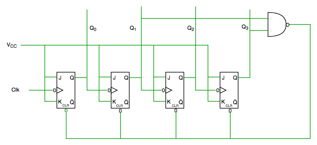
Decade counter circuit diagram
We see from circuit diagram that we have used nand gate for Q3 and Q1
and feeding this to clear input line because binary representation of
10 is—1010
And we see Q3 and Q1 are 1 here, if we give NAND of these two bits to clear input then counter will be clear at 10 and again start from beginning.
Important point: Number of flip flops used in counter are always greater than equal to (log2 n) where n=number of states in counter.
Some previous years gate questions on Counters
Q1. Consider the partial implementation of a 2-bitt counter using T flip-flops following the sequence 0-2-3-1-0, as shown below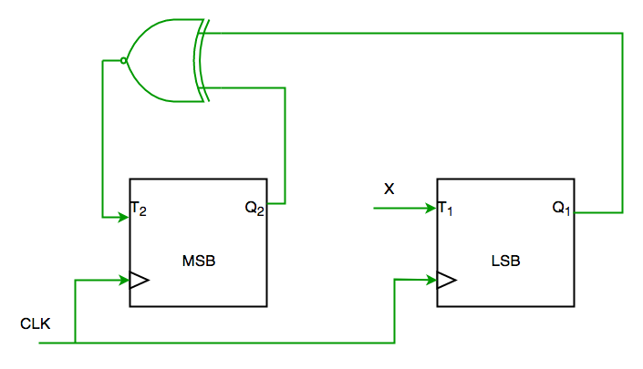
To complete the circuit, the input X should be
(A) Q2′
(B) Q2 + Q1
(C) (Q1 ⊕ Q2)’
(D) Q1 ⊕ Q2 (GATE-CS-2004)
Solution:
From circuit we see
T1=XQ1’+X’Q1—-(1)
AND
T2=(Q2 ⊕ Q1)’—-(2)
AND DESIRED OUTPUT IS 00->10->11->01->00
SO X SHOULD BE Q1Q2’+Q1’Q2 SATISFYING 1 AND 2.
SO ANS IS (D) PART.
Q2. The control signal functions of a 4-bit binary counter are given below (where X is “don’t care”)
The counter is connected as follows:
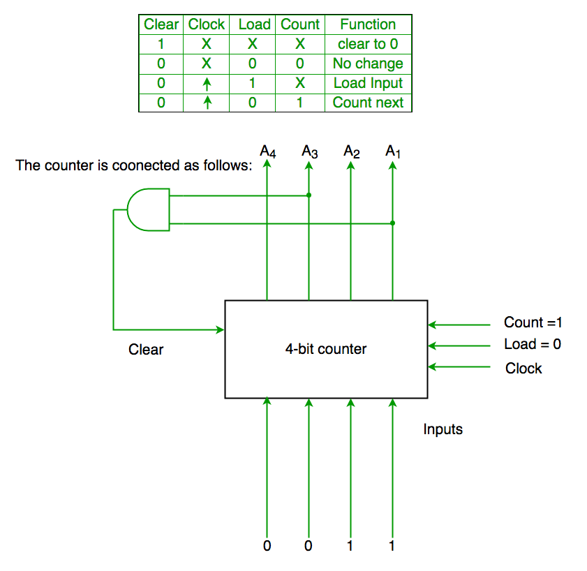
Assume that the counter and gate delays are negligible. If the counter starts at 0, then it cycles through the following sequence:
(A) 0,3,4
(B) 0,3,4,5
(C) 0,1,2,3,4
(D) 0,1,2,3,4,5 (GATE-CS-2007)
Solution:
Initially A1 A2 A3 A4 =0000
Clr=A1 and A3
So when A1 and A3 both are 1 it again goes to 0000
Hence 0000(init.) -> 0001(A1 and A3=0)->0010 (A1 and A3=0) -> 0011(A1 and A3=0) -> 0100 (A1 and A3=1)[ clear condition satisfied] ->0000(init.) so it goes through 0->1->2->3->4
Ans is (C) part.
Computer Organisation and Architecture
Generations of Computer
A computer is an electronic device that manipulates information or data. It has the ability to store, retrieve, and process data.
Nowadays, a computer can be used to type documents, send email, play games, and browse the Web. It can also be used to edit or create spreadsheets, presentations, and even videos. But the evolution of this complex system started around 1946 with the first Generation of Computer and evolving ever since.
Machine Instructions
Machine Instructions are commands or programs written in machine code of a machine (computer) that it can recognize and execute.
- A machine instruction consists of several bytes in memory that tells the processor to perform one machine operation.
- The processor looks at machine instructions in main memory one after another, and performs one machine operation for each machine instruction.
- The collection of machine instructions in main memory is called a machine language program.
The general format of a machine instruction is
| [Label:] Mnemonic [Operand, Operand] [; Comments] |
- Brackets indicate that a field is optional
- Label is an identifier that is assigned the address of the first byte of the instruction in which it appears. It must be followed by “:”
- Inclusion of spaces is arbitrary, except that at least one space must be inserted; no space would lead to an ambiguity.
- Comment field begins with a semicolon “ ; ”
| Here: MOV R5,#25H ;load 25H into R5 |
Machine instructions used in 8086 microprocessor
1. Data transfer instructions– move, load exchange, input, output.
- MOV :Move byte or word to register or memory .
- IN, OUT: Input byte or word from port, output word to port.
- LEA: Load effective address
- LDS, LES Load pointer using data segment, extra segment .
- PUSH, POP: Push word onto stack, pop word off stack.
- XCHG: Exchange byte or word.
- XLAT: Translate byte using look-up table.
2. Arithmetic instructions – add, subtract, increment, decrement, convert byte/word and compare.
- ADD, SUB: Add, subtract byte or word
- ADC, SBB :Add, subtract byte or word and carry (borrow).
- INC, DEC: Increment, decrement byte or word.
- NEG: Negate byte or word (two’s complement).
- CMP: Compare byte or word (subtract without storing).
- MUL, DIV: Multiply, divide byte or word (unsigned).
- IMUL, IDIV: Integer multiply, divide byte or word (signed)
- CBW, CWD: Convert byte to word, word to double word
- AAA, AAS, AAM,AAD: ASCII adjust for add, sub, mul, div .
- DAA, DAS: Decimal adjust for addition, subtraction (BCD numbers)
- NOT : Logical NOT of byte or word (one’s complement)
- AND: Logical AND of byte or word
- OR: Logical OR of byte or word.
- XOR: Logical exclusive-OR of byte or word
- TEST: Test byte or word (AND without storing).
- SHL, SHR: Logical Shift rotate instruction shift left, right byte or word? by 1or CL
- SAL, SAR: Arithmetic shift left, right byte or word? by 1 or CL
- ROL, ROR: Rotate left, right byte or word? by 1 or CL .
- RCL, RCR: Rotate left, right through carry byte or word? by 1 or CL.
- String manipulation instruction – load, store, move, compare and scan for byte/word
- MOVS: Move byte or word string
- MOVSB, MOVSW: Move byte, word string.
- CMPS: Compare byte or word string.
- SCAS S: can byte or word string (comparing to A or AX)
- LODS, STOS: Load, store byte or word string to AL.
- JMP:Unconditional jump .it includes loop transfer and subroutine and interrupt instructions.
- JNZ:jump till the counter value decreases to zero.It runs the loop till the value stored in CX becomes zero
- LOOP: Loop unconditional, count in CX, short jump to target address.
- LOOPE (LOOPZ): Loop if equal (zero), count in CX, short jump to target address.
- LOOPNE (LOOPNZ): Loop if not equal (not zero), count in CX, short jump to target address.
- JCXZ: Jump if CX equals zero (used to skip code in loop).
- Subroutine and Intrrupt instructions-
- CALL, RET: Call, return from procedure (inside or outside current segment).
- INT, INTO: Software interrupt, interrupt if overflow.IRET: Return from interrupt.
Flag manipulation:
- STC, CLC, CMC: Set, clear, complement carry flag.
- STD, CLD: Set, clear direction flag.STI, CLI: Set, clear interrupt enable flag.
- PUSHF, POPF: Push flags onto stack, pop flags off stack.
Sample GATE Question
Consider the sequence of machine instructions given below:MUL R5, R0, R1 DIV R6, R2, R3 ADD R7, R5, R6 SUB R8, R7, R4In the above sequence, R0 to R8 are general purpose registers. In the instructions shown, the first register stores the result of the operation performed on the second and the third registers. This sequence of instructions is to be executed in a pipelined instruction processor with the following 4 stages: (1) Instruction Fetch and Decode (IF), (2) Operand Fetch (OF), (3) Perform Operation (PO) and (4) Write back the Result (WB). The IF, OF and WB stages take 1 clock cycle each for any instruction. The PO stage takes 1 clock cycle for ADD or SUB instruction, 3 clock cycles for MUL instruction and 5 clock cycles for DIV instruction. The pipelined processor uses operand forwarding from the PO stage to the OF stage. The number of clock cycles taken for the execution of the above sequence of instructions is ___________
(A) 11
(B) 12
(C) 13
(D) 14
Answer: (C)
Explanation:
 1   2   3   4   5   6   7   8   9   10   11   12   13
  IF  OF  PO  PO  PO  WB
      IF  OF          PO  PO  PO  PO  PO   WB
          IF          OF                   PO   WB
              IF          OF                    PO   WB
What’s difference between 1’s Complement and 2’s Complement?
1’s complement of a binary number is another binary number obtained by toggling all bits in it, i.e., transforming the 0 bit to 1 and the 1 bit to 0.
Examples:
Let numbers be stored using 4 bits

1's complement of 7 (0111) is 8 (1000)
1's complement of 12 (1100) is 3 (0011)
2’s complement of a binary number is 1 added to the 1’s complement of the binary number.
Examples:
Let numbers be stored using 4 bits

2's complement of 7 (0111) is 9 (1001)
2's complement of 12 (1100) is 4 (0100)
These representations are used for signed numbers.
The main difference
between 1′ s complement and 2′ s complement is that 1′ s complement has
two representations of 0 (zero) – 00000000, which is positive zero (+0)
and 11111111, which is negative zero (-0); whereas in 2′ s complement,
there is only one representation for zero – 00000000 (+0) because if we
add 1 to 11111111 (-1), we get 00000000 (+0) which is the same as
positive zero. This is the reason why 2′ s complement is generally used.
Another difference is that while adding
numbers using 1′ s complement, we first do binary addition, then add in
an end-around carry value. But, 2′ s complement has only one value for
zero, and doesn’t require carry values.
Addressing Modes
Addressing Modes– The
term addressing modes refers to the way in which the operand of an
instruction is specified. The addressing mode specifies a rule for
interpreting or modifying the address field of the instruction before
the operand is actually executed.
Addressing modes for 8086 instructions are divided into two categories:1) Addressing modes for data
2) Addressing modes for branch
The 8086 memory addressing modes provide
flexible access to memory, allowing you to easily access variables,
arrays, records, pointers, and other complex data types. The key to
good assembly language programming is the proper use of memory
addressing modes.
An assembly language program instruction consists of two partsThe memory address of an operand consists of two components:
IMPORTANT TERMS
- Starting address of memory segment.
- Effective address or Offset: An offset is determined by adding any combination of three address elements: displacement, base and index.
- Displacement: It is an 8 bit or 16 bit immediate value given in the instruction.
- Base: Contents of base register, BX or BP.
- Index: Content of index register SI or DI.
Addressing modes used by 8086 microprocessor are discussed below:
- Implied mode:: In implied addressing the operand is
specified in the instruction itself. In this mode the data is 8 bits or
16 bits long and data is the part of instruction.Zero address
instruction are designed with implied addressing mode.
Example: CLC (used to reset Carry flag to 0)
- Immediate addressing mode (symbol #):In this mode data is present in address field of instruction .Designed like one address instruction format.
Note:Limitation in the immediate mode is that the range of constants are restricted by size of address field.
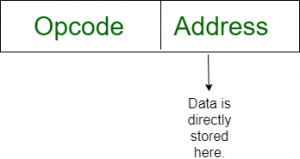
Example: MOV AL, 35H (move the data 35H into AL register)
- Register mode: In register addressing the operand
is placed in one of 8 bit or 16 bit general purpose registers. The data
is in the register that is specified by the instruction.
Here one register reference is required to access the data.
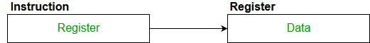
Example: MOV AX,CX (move the contents of CX register to AX register)
- Register Indirect mode: In this addressing the
operand’s offset is placed in any one of the registers BX,BP,SI,DI as
specified in the instruction. The effective address of the data is in
the base register or an index register that is specified by the
instruction.
Here two register reference is required to access the data.
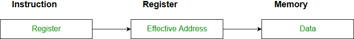
The 8086 CPUs let you access memory indirectly through a register using the register indirect addressing modes.MOV AX, [BX](move the contents of memory location s addressed by the register BX to the register AX)
- Auto Indexed (increment mode): Effective address of
the operand is the contents of a register specified in the instruction.
After accessing the operand, the contents of this register are
automatically incremented to point to the next consecutive memory
location.(R1)+.
Here one register reference,one memory reference and one ALU operation is required to access the data.
Example:Add R1, (R2)+ // OR R1 = R1 +M[R2] R2 = R2 + d
Useful for stepping through arrays in a loop. R2 – start of array d – size of an element - Auto indexed ( decrement mode): Effective address
of the operand is the contents of a register specified in the
instruction. Before accessing the operand, the contents of this register
are automatically decremented to point to the previous consecutive
memory location. –(R1)
Here one register reference,one memory reference and one ALU operation is required to access the data.
Example:
Add R1,-(R2)   //OR
R2 = R2-d
R1 = R1 + M[R2]
Auto decrement mode is same as auto increment mode. Both can also be used to implement a stack as push and pop . Auto increment and Auto decrement modes are useful for implementing “Last-In-First-Out” data structures.
Here only one memory reference operation is required to access the data.
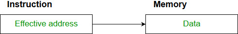
Example:ADD AL,[0301] //add the contents of offset address 0301 to AL
1st reference to get effective address.
2nd reference to access the data. Based on the availability of Effective address, Indirect mode is of two kind:
- Register Indirect:In this mode effective address is in the register,
and corresponding register name will be maintained in the address field
of an instruction.
Here one register reference,one memory reference is required to access the data. - Memory Indirect:In this mode effective address is in the memory, and
corresponding memory address will be maintained in the address field of
an instruction.
Here two memory reference is required to access the data.
Example:MOV AX, [SI +05]
Example: ADD AX, [BX+SI]
- PC relative addressing mode: PC relative addressing
mode is used to implement intra segment transfer of control, In this
mode effective address is obtained by adding displacement to PC.
EA= PC + Address field value
PC= PC + Relative value.
- Base register addressing mode:Base register
addressing mode is used to implement inter segment transfer of
control.In this mode effective address is obtained by adding base
register value to address field value.
EA= Base register + Address field value.
PC= Base register + Relative value.
Note:
- PC relative nad based register both addressing modes are suitable for program relocation at runtime.
- Based register addressing mode is best suitable to write position independent codes.
Sample GATE Question
Match each of the high level language statements given on the left
hand side with the most natural addressing mode from those listed on the
riright hand side.
1. A[1] = B[J]; a. Indirect addressing 2. while [*A++]; b. Indexed addressing 3. int temp = *x; c. Autoincrement(A) (1, c), (2, b), (3, a)
(B) (1, a), (2, c), (3, b)
(C) (1, b), (2, c), (3, a)
(D) (1, a), (2, b), (3, c)
Answer: (C)
Explanation:
List 1                           List 2
1) A[1] = B[J];      b) Index addressing
Here indexing is used

2) while [*A++];     c) auto increment
The memory locations are automatically incremented

3) int temp = *x;    a) Indirect addressing
Here temp is assigned the value of int type stored
at the address contained in X
Hence (C) is correct solution.
Cache Memory
Cache Memory in Computer Organization
Cache memory is used to reduce the average time to access data from the Main memory. The cache is a smaller and faster memory which stores copies of the data from frequently used main memory locations. There are various different independent caches in a CPU, which stored instruction and data.
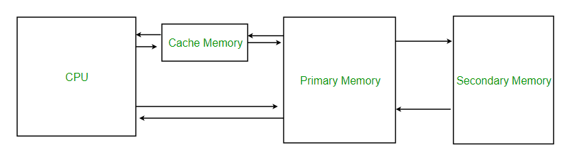
Levels of memory:
- Level 1 or Register –
It is a type of memory in which data is stored and accepted that are immediately stored in CPU. Most commonly used register is accumulator, Program counter, address register etc. - Level 2 or Cache memory –
It is the fastest memory which has faster access time where data is temporarily stored for faster access. - Level 3 or Main Memory –
It is memory on which computer works currently it is small in size and once power is off data no longer stays in this memory - Level 4 or Secondary Memory –
It is external memory which is not fast as main memory but data stays permanently in this memory
When the processor needs to read or write a location in main memory, it first checks for a corresponding entry in the cache.
- If the processor finds that the memory location is in the cache, a cache hit has occurred and data is read from cache
- If the processor does not find the memory location in the cache, a cache miss has occurred. For a cache miss, the cache allocates a new entry and copies in data from main memory, then the request is fulfilled from the contents of the cache.
Hit ratio = hit / (hit + miss) = no. of hits/total accessesWe can improve Cache performance using higher cache block size, higher associativity, reduce miss rate, reduce miss penalty, and reduce Reduce the time to hit in the cache.
Cache Mapping:
There are three different types of mapping used for the purpose of cache memory which are as follows: Direct mapping, Associative mapping, and Set-Associative mapping. These are explained as following below.
- Direct Mapping –
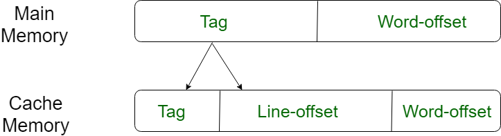
The simplest technique, known as direct mapping, maps each block of main memory into only one possible cache line. or
In Direct mapping, assigned each memory block to a specific line in the cache. If a line is previously taken up by a memory block when a new block needs to be loaded, the old block is trashed. An address space is split into two parts index field and a tag field. The cache is used to store the tag field whereas the rest is stored in the main memory. Direct mapping`s performance is directly proportional to the Hit ratio.i = j modulo m where i=cache line number j= main memory block number m=number of lines in the cache
For purposes of cache access, each main memory address can be viewed as consisting of three fields. The least significant w bits identify a unique word or byte within a block of main memory. In most contemporary machines, the address is at the byte level. The remaining s bits specify one of the 2s blocks of main memory. The cache logic interprets these s bits as a tag of s-r bits (most significant portion) and a line field of r bits. This latter field identifies one of the m=2r lines of the cache.
- Associative Mapping –
In this type of mapping, the associative memory is used to store content and addresses both of the memory word. Any block can go into any line of the cache. This means that the word id bits are used to identify which word in the block is needed, but the tag becomes all of the remaining bits. This enables the placement of any word at any place in the cache memory. It is considered to be the fastest and the most flexible mapping form.
- Set-associative Mapping –
This form of mapping is an enhanced form of direct mapping where the drawbacks of direct mapping are removed. Set associative addresses the problem of possible thrashing in the direct mapping method. It does this by saying that instead of having exactly one line that a block can map to in the cache, we will group a few lines together creating a set. Then a block in memory can map to any one of the lines of a specific set..Set-associative mapping allows that each word that is present in the cache can have two or more words in the main memory for the same index address. Set associative cache mapping combines the best of direct and associative cache mapping techniques. In this case, the cache consists of a number of sets, each of which consists of a number of lines. The relationships are
m = v * k
i= j mod v

where
i=cache set number
j=main memory block number
v=number of sets
m=number of lines in the cache number of sets
k=number of lines in each set

Application of Cache Memory –
- Usually, the cache memory can store a reasonable number of blocks at any given time, but this number is small compared to the total number of blocks in the main memory.
- The correspondence between the main memory blocks and those in the cache is specified by a mapping function.
Types of Cache –
- Primary Cache –
A primary cache is always located on the processor chip. This cache is small and its access time is comparable to that of processor registers. - Secondary Cache –
Secondary cache is placed between the primary cache and the rest of the memory. It is referred to as the level 2 (L2) cache. Often, the Level 2 cache is also housed on the processor chip.
Locality of reference –
Since size of cache memory is less as compared to main memory. So to check which part of main memory should be given priority and loaded in cache is decided based on locality of reference.
Types of Locality of reference
- Spatial Locality of reference
This says that there is a chance that element will be present in the close proximity to the reference point and next time if again searched then more close proximity to the point of reference. - Temporal Locality of reference
In this Least recently used algorithm will be used. Whenever there is page fault occurs within a word will not only load word in main memory but complete page fault will be loaded because spatial locality of reference rule says that if you are referring any word next word will be referred in its register that’s why we load complete page table so the complete block will be loaded.
GATE Practice Questions –
Que-1: A computer has a 256 KByte, 4-way set associative, write back data cache with the block size of 32 Bytes. The processor sends 32-bit addresses to the cache controller. Each cache tag directory entry contains, in addition, to address tag, 2 valid bits, 1 modified bit and 1 replacement bit. The number of bits in the tag field of an address is
(A) 11
(B) 14
(C) 16
(D) 27
Answer: (C)
Explanation:
Que-2: Consider the data given in previous question. The size of the cache tag directory is
(A) 160 Kbits
(B) 136 bits
(C) 40 Kbits
(D) 32 bits
Answer: (A)
Explanation:
Que-3: An 8KB direct-mapped write-back cache is organized as multiple blocks, each of size 32-bytes. The processor generates 32-bit addresses. The cache controller maintains the tag information for each cache block comprising of the following.
1 Valid bit
1 Modified bit
As many bits as the minimum needed to identify the memory block mapped in the cache. What is the total size of memory needed at the cache controller to store meta-data (tags) for the cache?
(A) 4864 bits
(B) 6144 bits
(C) 6656 bits
(D) 5376 bits
Answer: (D)
Computer Arithmetic | Set – 1
Negative Number Representation
- Sign Magnitude
Sign
magnitude is a very simple representation of negative numbers. In sign
magnitude the first bit is dedicated to represent the sign and hence it
is called sign bit.
Sign bit ‘1’ represents negative sign.
Sign bit ‘0’ represents positive sign.
In
sign magnitude representation of a n – bit number, the first bit will
represent sign and rest n-1 bits represent magnitude of number.
For example,
- +25 = 011001
Where 11001 = 25
And 0 for ‘+’
- -25 = 111001
Where 11001 = 25
And 1 for ‘-‘.
Range of number represented by sign magnitude method = -(2n-1-1) to +(2n-1-1) (for n bit number)
But there is one problem in sign magnitude and that is we have two representations of 0
+0 = 000000
– 0 = 100000
- 2’s complement method
To
represent a negative number in this form, first we need to take the 1’s
complement of the number represented in simple positive binary form and
then add 1 to it.
For example:
(8)10 = (1000)2
1’s complement of 1000 = 0111
Adding 1 to it, 0111 + 1 = 1000
So, (-8)10 = (1000)2
Please don’t get confused with (8)10 =1000 and (-8)10=1000 as with 4 bits, we can’t represent a positive number more than 7. So, 1000 is representing -8 only.
Range of number represented by 2’s complement = (-2n-1 to 2n-1 – 1)
Floating point representation of numbers
- 32-bit representation floating point numbers IEEE standard

Normalization
- Floating point numbers are usually normalized
- Exponent is adjusted so that leading bit (MSB) of mantissa is 1
- Since it is always 1 there is no need to store it
- Scientific notation where numbers are normalized to give a single digit before the decimal point like in decimal system e.g. 3.123 x 10³
Changing 3 in binary=11
Changing .625 in binary
Writing in binary exponent form.625 X 2 1.25 X 2 0.5 X 2 1
3.625=11.101 X 20
On normalizing
11.101 X 20=1.1101 X 21
On biasing exponent = 127 + 1 = 128
(128)10=(10000000) 2
For getting significandDigits after decimal = 1101
Expanding to 23 bit = 11010000000000000000000
Setting sign bit
As it is a positive number, sign bit = 0
Finally we arrange according to representation
Sign bit exponent significand
0 10000000 11010000000000000000000
- 64-bit representation floating point numbers IEEE standard

Again we follow the same procedure upto normalization. After that, we add 1023 to bias the exponent.
For example, we represent -3.625 in 64 bit format.
Changing 3 in binary = 11
Changing .625 in binary
.625 X 2       1

.25 X 2         0

.5 X 2           1
Writing in binary exponent form
3.625 = 11.101 X 20
On normalizing
11.101 X 20 = 1.1101 X 21
On biasing exponent 1023 + 1 = 1024
(1024)10 = (10000000000)2
So 11 bit exponent = 10000000000
52 bit significand = 110100000000 …………. making total 52 bits
Setting sign bit = 1 (number is negative)
So, final representation
1 10000000000 110100000000 …………. making total 52 bits by adding further 0’s
Converting floating point into decimal
Let’s convert a FP number into decimal
1 01111100 11000000000000000000000
The decimal value of an IEEE number is given by the formula:
(1 -2s) * (1 + f) * 2( e – bias )
where
- s, f and e fields are taken as decimal here.
- (1 -2s) is 1 or -1, depending upon sign bit 0 and 1
- add an implicit 1 to the significand (fraction field f), as in formula
First convert each individual field to decimal.
- The sign bit s is 1
- The e field contains 01111100 = (124)10
- The mantissa is 0.11000 … = (0.75)10
(1 – 2) * (1 + 0.75) * 2124 – 127 = ( – 1.75 * 2-3 ) = – 0.21875
Computer Arithmetic | Set – 2
FLOATING POINT ADDITION AND SUBTRACTION
- FLOATING POINT ADDITION
To understand floating point addition, first we see addition of real numbers in decimal as same logic is applied in both cases.
For example, we have to add 1.1 * 103 and 50.
We cannot add these numbers directly. First, we need to align the exponent and then, we can add significand.
After aligning exponent, we get 50 = 0.05 * 103
Now adding significand, 0.05 + 1.1 = 1.15
So, finally we get (1.1 * 103 + 50) = 1.15 * 103
Here, notice that we shifted 50 and made it 0.05 to add these numbers.
Now let us take example of floating point number addition
We follow these steps to add two numbers:
1. Align the significand
2. Add the significands
3. Normalize the result
Let the two numbers be
x = 9.75
y = 0.5625
y = 0.5625
Converting them into 32-bit floating point representation,
9.75’s representation in 32-bit format = 0 10000010 00111000000000000000000
0.5625’s representation in 32-bit format = 0 01111110 00100000000000000000000
Now we get the difference of exponents to know how much shifting is required.
(10000010 – 01111110)2 = (4)10
Now, we shift the mantissa of lesser number right side by 4 units.
Mantissa of 0.5625 = 1.00100000000000000000000
(note that 1 before decimal point is understood in 32-bit representation)
Shifting right by 4 units, we get 0.00010010000000000000000
Mantissa of 9.75 = 1. 00111000000000000000000
Adding mantissa of both
0. 00010010000000000000000
+ 1. 00111000000000000000000
————————————————-
1. 01001010000000000000000
In final answer, we take exponent of bigger number
So, final answer consist of :
Sign bit = 0
Exponent of bigger number = 10000010
Mantissa = 01001010000000000000000
32 bit representation of answer = x + y = 0 10000010 01001010000000000000000
- FLOATING POINT SUBTRACTION
Subtraction
is similar to addition with some differences like we subtract mantissa
unlike addition and in sign bit we put the sign of greater number.
Let the two numbers be
x = 9.75
y = – 0.5625
y = – 0.5625
Converting them into 32-bit floating point representation
9.75’s representation in 32-bit format = 0 10000010 00111000000000000000000
– 0.5625’s representation in 32-bit format = 1 01111110 00100000000000000000000
Now, we find the difference of exponents to know how much shifting is required.
(10000010 – 01111110)2 = (4)10
Now, we shift the mantissa of lesser number right side by 4 units.
Now, we shift the mantissa of lesser number right side by 4 units.
Mantissa of – 0.5625 = 1.00100000000000000000000
(note that 1 before decimal point is understood in 32-bit representation)
Shifting right by 4 units, 0.00010010000000000000000
Mantissa of 9.75= 1. 00111000000000000000000
Subtracting mantissa of both
0. 00010010000000000000000
– 1. 00111000000000000000000
————————————————
1. 00100110000000000000000
Sign bit of bigger number = 0
So, finally the answer = x – y = 0 10000010 00100110000000000000000

Cache Organization | Set 1 (Introduction)
Cache is close to CPU and faster than main memory. But at the same time is smaller than main memory. The cache organization is about mapping data in memory to a location in cache.
A Simple Solution:
One way to go about this mapping is to consider last few bits of long memory address to find small cache address, and place them at the found address.
Problems With Simple Solution:
The problem with this approach is, we loose the information about high order bits and have no way to find out the lower order bits belong to which higher order bits.
Solution is Tag:
To handle above problem, more information is stored in cache to tell which block of memory is stored in cache. We store additional information as Tag

What is a Cache Block?
Since programs have Spatial Locality (Once a location is retrieved, it is highly probable that the nearby locations would be retrieved in near future). So a cache is organized in the form of blocks. Typical cache block sizes are 32 bytes or 64 bytes.

The above arrangement is Direct Mapped Cache and it has following problem
We have discussed above that last few bits of memory addresses are being used to address in cache and remaining bits are stored as tag. Now imagine that cache is very small and addresses of 2 bits. Suppose we use the last two bits of main memory address to decide the cache (as shown in below diagram). So if a program accesses 2, 6, 2, 6, 2, …, every access would cause a hit as 2 and 6 have to be stored in same location in cache.

Solution to above problem – Associativity
What if we could store data at any place in cache, the above problem won’t be there? That would slow down cache, so we do something in between.

Pipelining | Set 1 (Execution, Stages and Throughput)
Computer Organization and Architecture | Pipelining | Set 1 (Execution, Stages and Throughput)
1) Improve the hardware by introducing faster circuits.
2) Arrange the hardware such that more than one operation can be performed at the same time.
Since, there is a limit on the speed of hardware and the cost of faster circuits is quite high, we have to adopt the 2nd option.
Pipelining : Pipelining is a process of arrangement of hardware elements of the CPU such that its overall performance is increased. Simultaneous execution of more than one instruction takes place in a pipelined processor.
Let us see a real life example that works on the concept of pipelined operation. Consider a water bottle packaging plant. Let there be 3 stages that a bottle should pass through, Inserting the bottle(I), Filling water in the bottle(F), and Sealing the bottle(S). Let us consider these stages as stage 1, stage 2 and stage 3 respectively. Let each stage take 1 minute to complete its operation.
Now, in a non pipelined operation, a bottle is first inserted in the plant, after 1 minute it is moved to stage 2 where water is filled. Now, in stage 1 nothing is happening. Similarly, when the bottle moves to stage 3, both stage 1 and stage 2 are idle. But in pipelined operation, when the bottle is in stage 2, another bottle can be loaded at stage 1. Similarly, when the bottle is in stage 3, there can be one bottle each in stage 1 and stage 2. So, after each minute, we get a new bottle at the end of stage 3. Hence, the average time taken to manufacture 1 bottle is :
Without pipelining = 9/3 minutes = 3m
I F S | | | | | |
| | | I F S | | |
| | | | | | I F S (9 minutes)
With pipelining = 5/3 minutes = 1.67m
I F S | |
| I F S |
| | I F S (5 minutes)
Thus, pipelined operation increases the efficiency of a system.
Design of a basic pipeline
- In a pipelined processor, a pipeline has two ends, the input end and the output end. Between these ends, there are multiple stages/segments such that output of one stage is connected to input of next stage and each stage performs a specific operation.
- Interface registers are used to hold the intermediate output between two stages. These interface registers are also called latch or buffer.
- All the stages in the pipeline along with the interface registers are controlled by a common clock.
Execution sequence of instructions in a pipelined processor can be visualized using a space-time diagram. For example, consider a processor having 4 stages and let there be 2 instructions to be executed. We can visualize the execution sequence through the following space-time diagrams:
Non overlapped execution:
| Stage / Cycle | 1 | 2 | 3 | 4 | 5 | 6 | 7 | 8 |
|---|---|---|---|---|---|---|---|---|
| S1 | I1 | I2 | ||||||
| S2 | I1 | I2 | ||||||
| S3 | I1 | I2 | ||||||
| S4 | I1 | I2 |
Overlapped execution:
| Stage / Cycle | 1 | 2 | 3 | 4 | 5 |
|---|---|---|---|---|---|
| S1 | I1 | I2 | |||
| S2 | I1 | I2 | |||
| S3 | I1 | I2 | |||
| S4 | I1 | I2 |
Pipeline Stages
RISC processor has 5 stage instruction pipeline to execute all the instructions in the RISC instruction set. Following are the 5 stages of RISC pipeline with their respective operations:
- Stage 1 (Instruction Fetch)
In this stage the CPU reads instructions from the address in the memory whose value is present in the program counter. - Stage 2 (Instruction Decode)
In this stage, instruction is decoded and the register file is accessed to get the values from the registers used in the instruction. - Stage 3 (Instruction Execute)
In this stage, ALU operations are performed. - Stage 4 (Memory Access)
In this stage, memory operands are read and written from/to the memory that is present in the instruction. - Stage 5 (Write Back)
In this stage, computed/fetched value is written back to the register present in the instructions.
Consider a ‘k’ segment pipeline with clock cycle time as ‘Tp’. Let there be ‘n’ tasks to be completed in the pipelined processor. Now, the first instruction is going to take ‘k’ cycles to come out of the pipeline but the other ‘n – 1’ instructions will take only ‘1’ cycle each, i.e, a total of ‘n – 1’ cycles. So, time taken to execute ‘n’ instructions in a pipelined processor:
                     ETpipeline = k + n – 1 cycles
                              = (k + n – 1) Tp
In the same case, for a non-pipelined processor, execution time of ‘n’ instructions will be:ETnon-pipeline = n * k * TpSo, speedup (S) of the pipelined processor over non-pipelined processor, when ‘n’ tasks are executed on the same processor is:
    S = Performance of pipelined processor /
        Performance of Non-pipelined processor
As the performance of a processor is inversely proportional to the execution time, we have, S = ETnon-pipeline / ETpipeline
=> S = [n * k * Tp] / [(k + n – 1) * Tp]
S = [n * k] / [k + n – 1]
When the number of tasks ‘n’ are significantly larger than k, that is, n >> k S = n * k / n
S = k
where ‘k’ are the number of stages in the pipeline.Also, Efficiency = Given speed up / Max speed up = S / Smax
We know that, Smax = k
So, Efficiency = S / k
Throughput = Number of instructions / Total time to complete the instructions
So, Throughput = n / (k + n – 1) * Tp
Note: The cycles per instruction (CPI) value of an ideal pipelined processor is 1
Please see Set 2 for Dependencies and Data Hazard and Set 3 for Types of pipeline and Stalling.
Pipelining | Set 2 (Dependencies and Data Hazard)
Computer Organization and Architecture | Pipelining | Set 2 (Dependencies and Data Hazard)
Dependencies in a pipelined processor
There are mainly three types of dependencies possible in a pipelined processor. These are :
1) Structural Dependency
2) Control Dependency
3) Data Dependency
These dependencies may introduce stalls in the pipeline.
Stall : A stall is a cycle in the pipeline without new input.
Structural dependency
This dependency arises due to the resource conflict in the pipeline. A resource conflict is a situation when more than one instruction tries to access the same resource in the same cycle. A resource can be a register, memory, or ALU.
Example:
| Instruction / Cycle | 1 | 2 | 3 | 4 | 5 |
|---|---|---|---|---|---|
| I1 | IF(Mem) | ID | EX | Mem | |
| I2 | IF(Mem) | ID | EX | ||
| I3 | IF(Mem) | ID | EX | ||
| I4 | IF(Mem) | ID |
To avoid this problem, we have to keep the instruction on wait until the required resource (memory in our case) becomes available. This wait will introduce stalls in the pipeline as shown below:
| Cycle | 1 | 2 | 3 | 4 | 5 | 6 | 7 | 8 |
|---|---|---|---|---|---|---|---|---|
| I1 | IF(Mem) | ID | EX | Mem | WB | |||
| I2 | IF(Mem) | ID | EX | Mem | WB | |||
| I3 | IF(Mem) | ID | EX | Mem | WB | |||
| I4 | – | – | – | IF(Mem) |
Solution for structural dependency
To minimize structural dependency stalls in the pipeline, we use a hardware mechanism called Renaming.
Renaming : According to renaming, we divide the memory into two independent modules used to store the instruction and data separately called Code memory(CM) and Data memory(DM) respectively. CM will contain all the instructions and DM will contain all the operands that are required for the instructions.
| Instruction/ Cycle | 1 | 2 | 3 | 4 | 5 | 6 | 7 |
|---|---|---|---|---|---|---|---|
| I1 | IF(CM) | ID | EX | DM | WB | ||
| I2 | IF(CM) | ID | EX | DM | WB | ||
| I3 | IF(CM) | ID | EX | DM | WB | ||
| I4 | IF(CM) | ID | EX | DM | |||
| I5 | IF(CM) | ID | EX | ||||
| I6 | IF(CM) | ID | |||||
| I7 | IF(CM) |
Control Dependency (Branch Hazards)
This type of dependency occurs during the transfer of control instructions such as BRANCH, CALL, JMP, etc. On many instruction architectures, the processor will not know the target address of these instructions when it needs to insert the new instruction into the pipeline. Due to this, unwanted instructions are fed to the pipeline.
Consider the following sequence of instructions in the program:
100: I1
101: I2 (JMP 250)
102: I3
.
.
250: BI1
Expected output: I1 -> I2 -> BI1
NOTE: Generally, the target address of the JMP instruction is known after ID stage only.
| Instruction/ Cycle | 1 | 2 | 3 | 4 | 5 | 6 |
|---|---|---|---|---|---|---|
| I1 | IF | ID | EX | MEM | WB | |
| I2 | IF | ID (PC:250) | EX | Mem | WB | |
| I3 | IF | ID | EX | Mem | ||
| BI1 | IF | ID | EX |
So, the output sequence is not equal to the expected output, that means the pipeline is not implemented correctly.
To correct the above problem we need to stop the Instruction fetch until we get target address of branch instruction. This can be implemented by introducing delay slot until we get the target address.
| Instruction/ Cycle | 1 | 2 | 3 | 4 | 5 | 6 |
|---|---|---|---|---|---|---|
| I1 | IF | ID | EX | MEM | WB | |
| I2 | IF | ID (PC:250) | EX | Mem | WB | |
| Delay | – | – | – | – | – | – |
| BI1 | IF | ID | EX |
As the delay slot performs no operation, this output sequence is equal to the expected output sequence. But this slot introduces stall in the pipeline.
Solution for Control dependency Branch Prediction is the method through which stalls due to control dependency can be eliminated. In this at 1st stage prediction is done about which branch will be taken.For branch prediction Branch penalty is zero.
Branch penalty : The number of stalls introduced during the branch operations in the pipelined processor is known as branch penalty.
NOTE : As we see that the target address is available after the ID stage, so the number of stalls introduced in the pipeline is 1. Suppose, the branch target address would have been present after the ALU stage, there would have been 2 stalls. Generally, if the target address is present after the kth stage, then there will be (k – 1) stalls in the pipeline.
Total number of stalls introduced in the pipeline due to branch instructions = Branch frequency * Branch Penalty
Data Dependency (Data Hazard)
Let us consider an ADD instruction S, such that
S : ADD R1, R2, R3
Addresses read by S = I(S) = {R2, R3}
Addresses written by S = O(S) = {R1}
Now, we say that instruction S2 depends in instruction S1, when
This condition is called Bernstein condition.
Three cases exist:
- Flow (data) dependence: O(S1) ∩ I (S2), S1 → S2 and S1 writes after something read by S2
- Anti-dependence: I(S1) ∩ O(S2), S1 → S2 and S1 reads something before S2 overwrites it
- Output dependence: O(S1) ∩ O(S2), S1 → S2 and both write the same memory location.
I1 : ADD R1, R2, R3
I2 : SUB R4, R1, R2
When the above instructions are executed in a pipelined processor, then data dependency condition will occur, which means that I2 tries to read the data before I1 writes it, therefore, I2 incorrectly gets the old value from I1.
| Instruction / Cycle | 1 | 2 | 3 | 4 |
|---|---|---|---|---|
| I1 | IF | ID | EX | DM |
| I2 | IF | ID(Old value) | EX |
Operand Forwarding : In operand forwarding, we use the interface registers present between the stages to hold intermediate output so that dependent instruction can access new value from the interface register directly.
Considering the same example:
I1 : ADD R1, R2, R3
I2 : SUB R4, R1, R2
| Instruction / Cycle | 1 | 2 | 3 | 4 |
|---|---|---|---|---|
| I1 | IF | ID | EX | DM |
| I2 | IF | ID | EX |
Data Hazards
Data hazards occur when instructions that exhibit data dependence, modify data in different stages of a pipeline. Hazard cause delays in the pipeline. There are mainly three types of data hazards:
1) RAW (Read after Write) [Flow/True data dependency]
2) WAR (Write after Read) [Anti-Data dependency]
3) WAW (Write after Write) [Output data dependency]
Let there be two instructions I and J, such that J follow I. Then,
-
RAW hazard occurs when instruction J tries to read data before instruction I writes it.
Eg:
I: R2 <- R1 + R3
J: R4 <- R2 + R3 -
WAR hazard occurs when instruction J tries to write data before instruction I reads it.
Eg:
I: R2 <- R1 + R3
J: R3 <- R4 + R5 -
WAW hazard occurs when instruction J tries to write output before instruction I writes it.
Eg:
I: R2 <- R1 + R3
J: R2 <- R4 + R5
Pipelining | Set 3 (Types and Stalling)
Computer Organization and Architecture | Pipelining | Set 3 (Types and Stalling)
Types of pipeline
- Uniform delay pipeline
In this type of pipeline, all the stages will take same time to complete an operation.
In uniform delay pipeline, Cycle Time (Tp) = Stage Delay If buffers are included between the stages then, Cycle Time (Tp) = Stage Delay + Buffer Delay - Non-Uniform delay pipeline
In this type of pipeline, different stages take different time to complete an operation.
In this type of pipeline, Cycle Time (Tp) = Maximum(Stage Delay) For example, if there are 4 stages with delays, 1 ns, 2 ns, 3 ns, and 4 ns, then
Tp = Maximum(1 ns, 2 ns, 3 ns, 4 ns) = 4 ns
If buffers are included between the stages,
Tp = Maximum(Stage delay + Buffer delay)
Example : Consider a 4 segment pipeline with stage delays (2 ns, 8 ns, 3 ns, 10 ns). Find the time taken to execute 100 tasks in the above pipeline.
Solution : As the above pipeline is a non-linear pipeline,
Tp = max(2, 8, 3, 10) = 10 ns
We know that ETpipeline = (k + n – 1) Tp = (4 + 100 – 1) 10 ns = 1030 ns
NOTE: MIPS = Million instructions per second
Performance of pipeline with stalls
Speed Up (S) = Performancepipeline / Performancenon-pipeline
=> S = Average Execution Timenon-pipeline / Average Execution Timepipeline
=> S = CPInon-pipeline * Cycle Timenon-pipeline / CPIpipeline * Cycle Timepipeline
Ideal CPI of the pipelined processor is ‘1’. But due to stalls, it becomes greater than ‘1’.
=>
S = CPInon-pipeline * Cycle Timenon-pipeline  / (1 + Number of stalls per Instruction) * Cycle Timepipeline

As Cycle Timenon-pipeline =   Cycle Timepipeline,

Speed Up (S) = CPInon-pipeline / (1 + Number of stalls per instruction)
__________________________________________________________________________________
Computer Organization | Hardwired v/s Micro-programmed Control Unit
Hardwired Control Unit –
The control hardware can be viewed as a state machine that changes from one state to another in every clock cycle, depending on the contents of the instruction register, the condition codes and the external inputs. The outputs of the state machine are the control signals. The sequence of the operation carried out by this machine is determined by the wiring of the logic elements and hence named as “hardwired”.
- Fixed logic circuits that correspond directly to the Boolean expressions are used to generate the control signals.
- Hardwired control is faster than micro-programmed control.
- A controller that uses this approach can operate at high speed.
- RISC architecture is based on hardwired control unit
Micro-programmed Control Unit –
- The control signals associated with operations are stored in special memory units inaccessible by the programmer as Control Words.
- Control signals are generated by a program are similar to machine language programs.
- Micro-programmed control unit is slower in speed because of the time it takes to fetch microinstructions from the control memory.
- Control Word : A control word is a word whose individual bits represent various control signals.
- Micro-routine : A sequence of control words corresponding to the control sequence of a machine instruction constitutes the micro-routine for that instruction.
- Micro-instruction : Individual control words in this micro-routine are referred to as microinstructions.
- Micro-program : A sequence of micro-instructions is called a micro-program, which is stored in a ROM or RAM called a Control Memory (CM).
- Control Store : the micro-routines for all instructions in the instruction set of a computer are stored in a special memory called the Control Store.
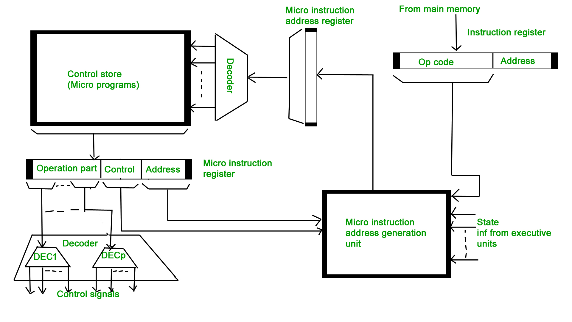
Types of Micro-programmed Control Unit – Based on the type of Control Word stored in the Control Memory (CM), it is classified into two types :
1. Horizontal Micro-programmed control Unit :
The control signals are represented in the decoded binary format that is 1 bit/CS. Example: If 53 Control signals are present in the processor than 53 bits are required. More than 1 control signal can be enabled at a time.
- It supports longer control word.
- It is used in parallel processing applications.
- It allows higher degree of parallelism. If degree is n, n CS are enabled at a time.
- It requires no additional hardware(decoders). It means it is faster than Vertical Microprogrammed.
- It is more flexible than vertical microprogrammed
The control signals re represented in the encoded binary format. For N control signals- Log2(N) bits are required.
- It supports shorter control words.
- It supports easy implementation of new conrol signals therefore it is more flexible.
- It allows low degree of parallelism i.e., degree of parallelism is either 0 or 1.
- Requires an additional hardware (decoders) to generate control signals, it implies it is slower than horizontal microprogrammed.
- It is less flexible than horizontal but more flexible than that of hardwired control unit.
__________________________________________________________________________________
Peripherals Devices in Computer Organization
Generally peripheral devices, however, are not essential for the computer to perform its basic tasks, they can be thought of as an enhancement to the user’s experience. A peripheral device is a device that is connected to a computer system but is not part of the core computer system architecture. Generally, more people use the term peripheral more loosely to refer to a device external to the computer case.
Classification of Peripheral devices:
It is generally classified into 3 basic categories which are given below:
- Input Devices:
The input devices is defined as it converts incoming data and instructions into a pattern of electrical signals in binary code that are comprehensible to a digital computer.
Example:Keyboard, mouse, scanner, microphone etc.
- Output Devices:
An output device is generally reverse of the input process and generally translating the digitized signals into a form intelligible to the user. The output device is also performed for sending data from one computer system to another. For some time punched-card and paper-tape readers were extensively used for input, but these have now been supplanted by more efficient devices.
Example:Monitors, headphones, printers etc.
- Storage Devices:
Storage devices are used to store data in the system which is required for performing any operation in the system. The storage device is one of the most requirement devices and also provide better compatibility.
Example:Hard disk, magnetic tape, Flash memory etc.
Peripherals devices provides more feature due to this operation of the system is easy. These are given below:
- It is helpful for taking input very easily.
- It is also provided a specific output.
- It has a storage device for storing information or data
- It also improves the efficiency of the system.
__________________________________________________________________________________
Basics of Computer and its Operations
- Accept data
- Store data
- Process data as desired
- Retrieve the stored data as and when required
- Print the result in desired format.
Data: It is the term used for raw facts and figures fed into the computer and along with the set of instructions which enables the computer to convert this raw data into the refined and useful information.
Information: Data represented in useful and meaningful form is information.
Classification of Computers:
Computers can be classified based on the technology being used and the way they are designed to perform the various tasks. Computers can be categorized into Digital, Analog and Hybrid based on their design and working:
- Digital Computers : These are the modern computers which are capable of processing information in discrete form. In digital technology data which can be in the form of letters, symbols or numbers is represented in binary form i.e. 0s and 1s. The digital computers are used in industrial, business and scientific applications. They are quite suitable for large volume data processing.
- Analog Computers : These computers are used to process data generated by ongoing physical processes. A thermometer is an example of an analog computer since it measures the change in mercury level continuously. Analog computers are well suited to simulating systems. A simulator helps to conduct experiments repeatedly in real time environment. Some of the common examples are simulations in aircrafts, nuclear power plants, hydraulic and electronic networks.
- Hybrid Computers : These use both analog and digital technology. It has the speed of analog computer and the accuracy of a digital computer. It may accept digital or analog signals but an extensive conversion of data from digital to analog and analog to digital has to be done. Hybrid Computers are used as a cost effective means for complex simulations.
Classification of Digital Computers
Example: portable computers such as PDAs (Personal Digital Assistants) and tablets
Peripheral Devices
These devices are used for performing the specific functions and are
connected to the computer externally. These peripheral devices enable
the computer to operate according to the user requirements by feeding
data in and out of the computer. Peripheral devices are as follows:- INPUT DEVICES : These devices accept data and instructions from the user. These include:
- Keyboard
- Mouse
- Light Pen
- Optical/magnetic Scanner
- Touch Screen
- Microphone for voice as input
- Track Ball
- Monitor (Visual Display Unit)
- Printers
- Plotter
- Speakers
Difference between RAM and Hard-disk
| RAM | Hard Disk |
|---|---|
| RAM is an electronic device | Hard-disk is an electromechanical device |
| Electronic device are faster in speed | Electro-mechanical device has speed slower than Electronic device. |
| CPU is an electronic device,so it’s speed can match with RAM.Therefore,CPU and RAM have connections and that connections is known as buses | Hard disk is an electro-mechanical device.Therefore,it’s speed cannot be match by CPU and hence their is no connection between hard-disk and CPU. |
Types of Software
- System Software : These are those software,without which our PC,laptop won’t run, i.e it is must for a device to be operating.
For Example: Linux,Unix,Windows,etc. - Application Software : These are those
software,without which our PC,laptop can run, i.e these software are
not necessary for a device to be operating.
For Example: Facebook,What’s App,Games.
NOTE: In Earlier times i.e before 1970s,for making both these software we have to learn different languages.
For Example, Assembly language was used for System Software whereas Pascal,Cubel,etc. were used for making Application Software.
Difference between Hacker and Cracker
- Hacker : They will just warn you something about malicious activity going around in your computer.It will not steal your information.
- Cracker : They will try to steal your Information without informing you.
__________________________________________________________________________________
ROS ( ROBOT OPERATING SYSTEM )
Robotics deals with the design, construction, operation, and use of robots, as well as computer systems for their control, sensory feedback, and information processing. These technologies are used to develop machines that can substitute for humans and replicate human actions.
ROS is an open-source, meta-operating system for your robot. It provides the services you would expect from an operating system, including hardware abstraction, low-level device control, implementation of commonly-used functionality, message-passing between processes, and package management .
ROS is designed to be a loosely coupled system where a process is called a node and every node should be responsible for one task. Nodes communicate with each other using messages passing via logical channels called topics ,
Robot Operating System (ROS or ros) is robotics middleware (i.e. collection of software frameworks for robot software development).
There are six main types of industrial robots: cartesian, SCARA, cylindrical, delta, polar and vertically articulated. However, there are several additional types of robot configurations. Each of these types offers a different joint configuration. The joints in the arm are referred to as axes.
Discuss three of the five major fields of robotics (human-robot interface, mobility, manipulation, programming, sensors) and their importance to robotics development.
ROS, which means Robot Operating System, is a set of software libraries and tools to help you build robot applications. The point of ROS is to create a robotics standard, so you don't need to reinvent the wheel anymore when building a new robotic software. So, why should you use ROS for robotics
The Robot Operating System (ROS), open-source middleware, has been widely used for robotics applications. However, the ROS is not suitable for real-time embedded systems because it does not satisfy real-time requirements and only runs on a few OSs.
Running ROS Software on Windows. ROS is currently not supported on Windows, but it is possible to run parts of ROS on Windows. In particular, you can: run some of the Python code, including the ROS client library for Python (rospy).
Although ROS stands for “Robot Operating System”, it is not an operating system. At least not as intended when talking about Linux. ROS is actually a set of software libraries, tools, and conventions (including protocols) made to ease the development of robotic applications .
Some of the important components of Robots are as follows:
- Manipulator: Just like the human arm, the robot consists of what is called a manipulator having several joints and links. ...
- Endeffector: ADVERTISEMENTS: ...
- The Locomotion Device: ...
- The Controller: ...
- The Sensors:
A ROS driver is a ROS node that makes a piece of hardware accessible from ROS. For example, it talks to a laser scanner and publishes the output of the device as ROS messages. ... In that case, it is called a ROS wrapper.
Robot Operating System (ROS or ros) is robotics middleware (i.e. collection of software frameworks for robot software development). Although ROS is not an operating system, it provides services designed for a heterogeneous computer cluster such as hardware abstraction, low-level device control, implementation of commonly used functionality, message-passing between processes, and package management. Running sets of ROS-based processes are represented in a graph architecture where processing takes place in nodes that may receive, post and multiplex sensor data, control, state, planning, actuator, and other messages. Despite the importance of reactivity and low latency in robot control, ROS itself is not a real-time OS (RTOS). It is possible, however, to integrate ROS with real-time code. The lack of support for real-time systems has been addressed in the creation of ROS 2.0, a major revision of the ROS API which will take advantage of modern libraries and technologies for core ROS functionality and add support for real-time code and embedded hardware.
Software in the ROS Ecosystem can be separated into three groups:
- language-and platform-independent tools used for building and distributing ROS-based software;
- ROS client library implementations such as roscpp, rospy, and roslisp;
- packages containing application-related code which uses one or more ROS client libraries.
The main ROS client libraries are geared toward a Unix-like system, primarily because of their dependence on large collections of open-source software dependencies. For these client libraries, Ubuntu Linux is listed as "Supported" while other variants such as Fedora Linux, macOS, and Microsoft Windows are designated "experimental" and are supported by the community. The native Java ROS client library, rosjava, however, does not share these limitations and has enabled ROS-based software to be written for the Android OS.] rosjava has also enabled ROS to be integrated into an officially supported MATLAB toolbox which can be used on Linux, macOS, and Microsoft Windows. A JavaScript client library, roslibjs has also been developed which enables integration of software into a ROS system via any standards-compliant web browser.

An image depicting the ROS equation: Plumbing + Tools + Capabilities + Ecosystem = ROS!
ROS was designed with open-source in mind, intending that users would be able to choose the configuration of tools and libraries which interacted with the core of ROS so that users could shift their software stacks to fit their robot and application area. As such, there is very little which is actually core to ROS, beyond the general structure within which programs must exist and communicate. In one sense, ROS is the underlying plumbing behind nodes and message passing. However, in reality, ROS is that plumbing, a rich and mature set of tools, a wide-ranging set of robot-agnostic capabilities provided by packages, and a greater ecosystem of additions to ROS.
Most robots are composed of 3 main parts:
- The Controller ‐ also known as the "brain" which is run by a computer program. ...
- Mechanical parts ‐ motors, pistons, grippers, wheels, and gears that make the robot move, grab, turn, and lift. ...
- Sensors ‐ to tell the robot about its surroundings.
Basic Components of a Robot
The components of a robot are the body/frame, control system, manipulators, and drivetrain.
A robot is made up of the very same components. A typical robot
has a movable physical structure, a motor of some sort, a sensor
system, a power supply and a computer "brain" that controls all of these
elements.
A robot's control system uses feedback just as the human brain does. However, instead of a collection of neurons, a robot's brain consists of a silicon chip called a central processing unit, or CPU, that is similar to the chip that runs your computer.
9 Jobs That Are Being Taken Over by Robots
- Long-haul truck drivers. ...
- Taxi, ride-hailing, and delivery drivers. ...
- Customer service and office assistants. ...
- Healthcare workers. ...
- Warehouse workers. ...
- Assembly line manufacturing. ...
- Retail and customer interaction jobs. ...
- Writers.
The arm is the main section of the robotic arm and consists of three parts: the shoulder, elbow and wrist. These are all joints, with the shoulder resting at the base of the arm, typically connected to the controller, and it can move forward, backward or spin. .
For robots, aluminum and steel are the most common metals. Aluminum is a softer metal and is therefore easier to work with, but steel is several times stronger. In any case, because of the inherent strength of metal, robot bodies can be made using sheet, bar, rod, channel, and other shapes.
The following robotic applications are the most common in the automotive industry:
- Collaborative Robots. These collaborative robots are built to work together with other robots, on enormous assembly lines. ...
- Robotic Painting. ...
- Robotic Welding. ...
- Robotic Assembly. ...
- Material Removal. ...
- Part Transfer and Machine Tending.
A Robot, in essence, is a Computer but a Computer is not essentially a Robot. Any Electronic device that is capable of carrying out instructions given by a human or through cascading and perform operations from basic Arithmetic, Logical etc to advanced Gaming and Virtualization and give O/P to user is a Computer.
the body of a robot called?
A humanoid robot is a robot with its body shape built to resemble the human body. ... In general, humanoid robots have a torso, a head, two arms, and two legs, though some forms of humanoid robots may model only part of the body, for example, from the waist up.
Robotics deals with the design, construction, operation, and use of robots, as well as computer systems for their control, sensory feedback, and information processing. These technologies are used to develop machines that can substitute for humans and replicate human actions.
Robots and AI will actually create more jobs than they take. ROBOTS will make more jobs than they take in the UK, according to a new report. The combination of artificial intelligence and robotics will displace up to 7 million jobs between 2017 and 2037.
the different fields of robotics?
Contributing fields
- Aerospace –
- Biology – Biomechanics –
- Computer science – ...
- Engineering – ...
- Fiction – Robotics technology and its implications are major themes in science fiction and have provided inspiration for robotics development and cause for ethical concerns. ...
- Military science –
- Psychology – ...
- Philosophy –
Robots are a good way to implement the lean principle in an industry. They save time as they can produce more products. They also reduce the amount of wasted material used due to the high accuracy.
An artificial brain (or artificial mind) is software and hardware with cognitive abilities similar to those of the animal or human brain. ... The ultimate goal of creating a machine exhibiting human-like behavior or intelligence is sometimes called strong AI.
The data points aren't there for us to understand, even if it's possible to transplant a human brain into a robot, what it's like to be a human brain transplanted into a robot.
"The objective of space robots is basically to perform an action in space such as position an instrument to take a measurement, collect a sample for examination, assemble a structure or even move around an astronaut." ... Types of robots The most conventional robot used in space missions is the rover.
NASA uses robots in many different ways. Robotic arms on spacecraft are used to move very large objects in space. Spacecraft that visit other worlds are robots that can do work by themselves. ... This type of robot includes the rovers that explore the surface of Mars .
For a long time the need for sleep has been considered by computer scientists as a biological characteristic without practical interest (in science-fiction novels, robots do not sleep). According to our first results, it appears to be a remarkable strategy of adaptation to a complex and continuously evolving world.
A robotic spacecraft is an uncrewed spacecraft, usually under telerobotic control. A robotic spacecraft designed to make scientific research measurements is often called a space probe. ... Many artificial satellites are robotic spacecraft, as are many landers and rovers.
A space probe is a robotic spacecraft that does not orbit Earth, but instead, explores further into outer space.
A robotic spacecraft is an uncrewed spacecraft with no humans on board, that is usually under telerobotic control. A robotic spacecraft designed to make scientific research measurements is often called a space probe.
_________________________________________________________________________________
UTC on ELECTRONICS ROBOTICS
Gen . MAC TECH Zone MARIA PREFER Within e- STAR_C
and Watch out e- S H I N to A / D / S Tour Route
__________________________________________________________________________________
Tidak ada komentar:
Posting Komentar