MARIA PREFER on energy efficiency and effectiveness in reviewing the meeting points of the elasticity of electrons that affect the working system of electronic circuits, starting from large currents to small to wireless and EINSTEIN PROG :
1. electrical cable connection point
2. Solder point on the PCB board
3. hot spot points on wireless networks and the internet
4. satellite as an electronic network server point.
MARIA PREFER is very much shaped by the continuous arrangement of electrons and photons of photons that make up MARIA PREFER' description so that it becomes more accurate and slow.
LOVE and JESI__ ISE
Gen . MAC TECH Zone EINSTEIN PROGRAM VIEW
--------------------------------------------------------------------------------------------------------------------------
The 3 Rules, The Humble Circuit, and Its Place in Our World of Electronics
Before diving into a complete circuit, it’s wise to first wrap your mind around the individual pieces that make up the whole, being flow, load, and conductivity. We’ve organized these principles into three basic rules:- Rule 1 – Electricity will always want to flow from a higher voltage to a lower voltage.
- Rule 2 – Electricity always has work that needs to be done.
- Rule 3 – Electricity always needs a path to travel.
Rule 1 – It’s All About the Flow
Every electronic circuit needs some a power source, whether that’s from an AA battery that you can pop into your Xbox One controller or something with a bit more force like your wall outlet that can power a large number of devices. The electricity that comes flowing out from these sources is measured in voltage, or volts, or simply V. .Regardless of where this power flows from, its purpose is always the same – to get from one area to another, and in the process to do some work, like charging your computer or turning on your lights.
The fundamental component of this flow of power is that electricity will always want to flow from a higher voltage to a lower voltage. Always. This is called potential. You could say that it’s the potential electricity has to move from one area to another.

Flow of High (Positive) Voltage to Low (Negative) Voltage.
- A battery has two sides, the negative side is the low voltage, measuring in at 0v, the positive side is the high voltage, measuring in at 1.5v.
- Energy will always want to flow out of the positive side of the battery to get to the negative side to find balance.
- To do this, it needs to flow along something, usually a copper wire, and do some work in the process, like turn on a light or spin a motor.
This all amounts to Rule 1 – Electricity will always want to flow from a higher voltage to a lower voltage. Remember this; it will never change.
Rule 2 – Getting Some Work Done
Now, you might have some electricity that wants to flow from a higher voltage to a lower voltage, but what’s the point? The only reason to make electricity flow is to give it some work to do. This process of electricity doing work in a circuit is called load. Without having a load, or some work for electricity to do, then there is no point in having a circuit. A load can be anything you can imagine, such as:- Spinning a motor which turns the propellers of a drone.
- Turning on a LED on a charging cable to indicate that your laptop is plugged in.
- Connecting your headset wirelessly with your laptop to listen to music.

Tis’ the season, electric load comes in many forms, one of which is powering these LEDs. (Image source)
Remember Rule 2 – Electricity always has work that will need to be done. Without work, then a circuit has no use.
Rule 3 – Following a Path
The third and final rule is what makes the first two rules possible – electricity needs a path to travel. This path acts as a kind of middleman. Let’s say you plug your laptop charger into a wall socket, and then into your laptop. It charges, obviously, but without that cord between your computer and wall outlet, nothing would happen.This is because electricity needs a path to follow to get from one destination to another. And the journey is always the same:
- Power – Electricity always starts from a source, like a battery or an outlet.
- Journey – It then takes its journey along a path, doing its work along the way.
- Destination – It then arrives at its final destination, finding rest at the lowest voltage point.

See all of those copper wires? Electricity loves traveling on this conductive material.
Putting It All Together – The Complete Circuit
Let’s put all of these rules together now in a complete definition of a circuit.A circuit is simply a path that electricity can flow through.
And with that simple concept right there, men and women have gone on to build some insanely complex circuits that have sent the human race to space and the depths of our deepest oceans. For now, we’ll keep things simple and put together our first circuit. Here’s what you’ll need if you want to follow along:
- (1) 9-volt battery
- (1) 470 Ω resistor
- (1) Generic LED
- (3) Test leads with alligator clips
Step 1 – Adding a Power Source
Going back to our Rule of Three’s, the first says that electricity will always want to flow from a higher voltage to a lower voltage. Okay, so this means we need some kind of power source in this circuit, we’ll add our 9v battery.
The beginning of our circuit starts with a 9v battery.
Step 2 – Adding Some Work
We now want our electricity to do some work for us before it can come to rest, so let’s have it turn on a simple LED light. You’ve likely seen these everywhere, in your Christmas tree, flashlights, light bulbs, etc… So we’ll take this LED and place it on the other side of our battery.Now, the one thing to mention about a LED is that it’s really sensitive and can’t have too much power running through it, so we need to add what’s called a resistor. We won’t go into the details now, but just know that a resistor will do like its name says – resist the flow of electricity enough for our LED to handle it. Let’s place that resistor to the left of our LED.

Adding some work to our circuit with a LED and resistor.
Step 3 – Providing a Path
This part is simple, we just need to connect our alligator clips between all of the components on our circuit. If you do this correctly, then your LED will shine bright! Remember, when connecting wires to a battery, always connect the positive end first, then the negative. Check out the picture below for how it all needs to be connected together.
Our electricity now has a path to flow through with the added alligator clips
Types of Circuits
Now, before you go running off into the wild and building your own circuits, you need to know about two ways to describe a circuit, one of which might ruin your circuit’s day, they include:Closed or Open Circuit
A circuit is considered a closed circuit when there is a complete path available for electricity to travel on. This is also referred to as a complete circuit. Now, if your circuit isn’t working as intended, then this means that it’s an open circuit. This can be caused by several things, including a loose connection or a broken wire.Here’s an easy, visual way to understand the difference between a closed or open circuit, check out the circuit diagram below and notice that it’s the same circuit we made above, except now it has a switch.

Here’s a diagram of the circuit we made above. Notice the addition of a switch.

Now our switch is triggered, which completes the circuit, allowing electricity to flow to our LED!
Short Circuit
Then there’s the short circuit. When you don’t give your circuit any work to do, but you still provide some power, prepare for some problems. Check out our circuit below, we took out the LED, resistor, and switch, leaving just our copper wire and battery.
Here’s a circuit well on its way to becoming a short circuit! Without any work to do this battery will soon burn out.
But the minute you take any of that work out of your circuit, the electricity goes crazy and runs around its path at full speed without anything holding it back. If you let this happen for an extended period of time, then you’ll find yourself with a damaged power supply, a drained battery, or maybe something even worse, like a fire!

Whoa! Don’t try this at home. Here’s a hefty 12v lantern battery being short-circuited in the name of science. (Image source)
You Are Now Dangerous
There you go, young electronics master, you now have all the information you need to control the humble circuit. By understanding how a circuit works, you’ll soon be able to tackle projects of all shapes and sizes. But before beginning your own journey, remember the Guiding Rule of Threes:- Rule 1 – Electricity will always want to flow from a higher voltage to a lower voltage.
- Rule 2 – Electricity always has work that needs to be done.
- Rule 3 – Electricity always needs a path to travel on.
__________________________________________________________________________________
A connection point is a point in an electrical connector where a cable begins or ends. ... You can use one connection point to represent all of the connector's pins, and route all wires or cables to that connection point. The pin connectivity data is held as internal data.
The part of a cable that plugs into a port or interface to connect one device to another. Most connectors are either male (containing one or more exposed pins) or female (containing holes in which the male connector can be inserted).
Terminal blocks are modular, insulated blocks that secure two or more wires together. ... Terminals are useful for connecting wiring to a ground or, in the case of electrical power, for connecting electrical switches and outlets to the mains.
Analog Audio Connectors:
- RCA Connectors: ...
- XLR Connectors: ...
- XLR Male: This is used to connect a variety of hardware inputs.
- XLR Female: It is used to connect a microphone and a variety of hardware inputs.
- TRS: It is used to connect both input and output devices.
- ¼” Audio Connectors: ...
- S/PDIF: ...
- AES/EBU:
The following cabling media types will be most commonly seen in LAN environments.
- Unshielded Twisted Pair (UTP) ...
- Shielded Twisted Pair (STP) ...
- Multi-Mode Fiber (MMF) ...
- Single Mode Fiber (SMF) ...
- Registered Jack 45 (RJ45) ...
- Straight Tip (ST) ...
- Subscriber Connector (SC) ...
- Lucent Connector (LC)
Three Types Of Cable Joints
There are three main types of electrical joints,
also known as splices: The Western Union splice, the tap splice and the
fixture splice. The Western Union splice connects two conductors
together and is particularly useful in repairing a broken wire.People often have difficulty choosing the correct gender termination on cable assemblies. Plugs are considered male gendered connectors which utilize a center pin. Jacks are considered female gendered connectors utilizing a center socket. What is the difference between a plug and a jack?
Slots and ports are physical connection points that allow the hardware of a computer to be expanded. A port is a socket. A slot is a dock for a printed circuit board. This board contains a port and fits into a slot.
Connection Points for Electrical Connectors
Connector Basics
Introduction
Connectors are used to join subsections of circuits together. Usually, a connector is used where it may be desirable to disconnect the subsections at some future time: power inputs, peripheral connections, or boards which may need to be replaced. .Connector Terminology
Before we get started discussing some commonly used connectors, let's explore the terminology used to describe connectors.Gender
Gender - The gender of a connector refers to whether it plugs in or is plugged into and is typically male or female, respectively (kids, ask your parents for a more thorough explanation). Unfortunately, there are cases where a connector may be referred to as "male" when it would appear to be female; in the examples section, we'll point a few of those out as we discuss individual component types and explain why that's the case.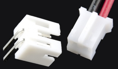
Male (left) and female 2.0mm PH series JST connectors. In this case, gender is determined by the individual conductor.
Polarity
Polarity - Most connectors can only be connected in one orientation. This trait is called polarity, and connectors which have some means to prevent them being connected wrong are said to be polarized, or sometimes keyed.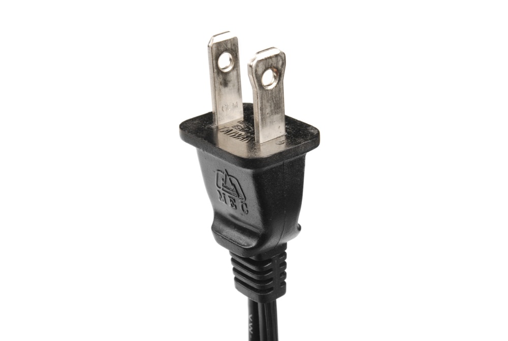
A polarized North
American wall plug. By having two different widths for the plug blades,
the plug will only go into the outlet one way.
Contact
Contact - Contacts are the business portion of the connector. They are the metal parts which touch each other, forming an electrical connection. This is also where problems occur: the contacts can become soiled or oxidized, or the springiness required to hold the contacts together may fade with time.
The contacts on this connector are clearly visible.
Pitch
Pitch - Many connectors consist of an array of contacts in a repeated pattern. The pitch of the connector is the distance from the center of one contact to the center of the next. This is important, because there are many families of contacts which look very similar but may differ in pitch, making it difficult to know that you are purchasing the right mating connector.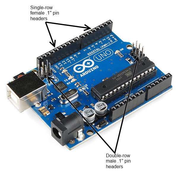
The pitch of the pins on the headers on a standard Arduino is .1".
Mating Cycles
Mating cycles - Connectors have a finite life, and connecting and disconnecting them is what wears them out. Datasheets usually present that information in terms of mating cycles, and it varies widely from one technology to another. A USB connector may have a lifetime in the thousands or tens of thousands of cycles, while a board-to-board connector designed for use inside of consumer electronics may be limited to tens of cycles. It's important that you select a connector with a suitable life for the application.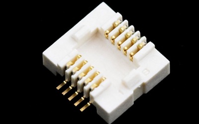
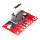
Mating connector for the GS406 GPS module. The connector's datasheet indicates a maximum of 50 insertion cycles for this part.
Mount
Mount - This one has the potential for being confusing. The term "mount" can refer to several things: how the connector is mounted in use (panel mount, free-hanging, board mount), what the angle of the connector is relative to its attachment (straight or right-angle), or how it is mechanically attached (solder tab, surface mount, through hole). We'll discuss this more in the examples section for each individual connector.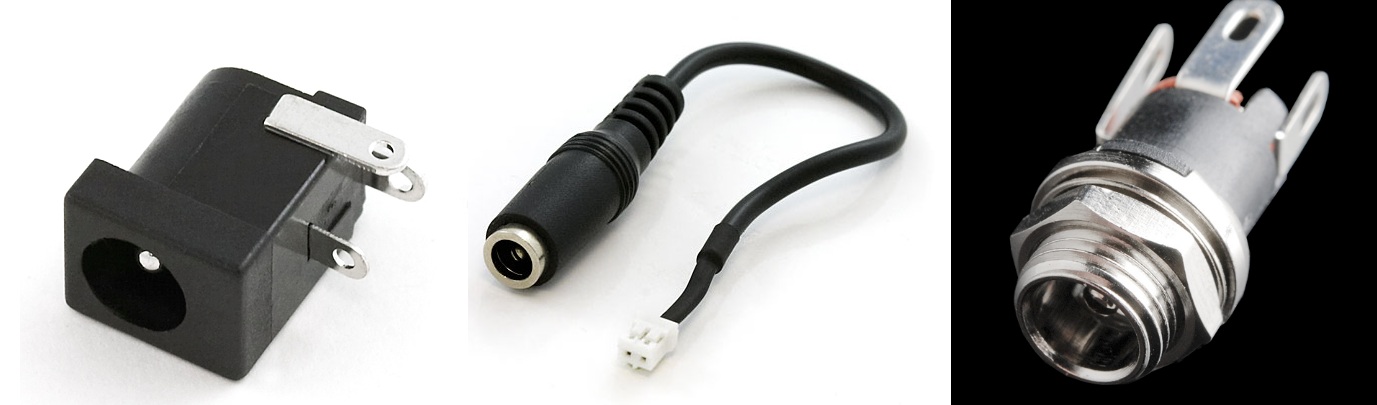
A comparison of three
different methods of mounting the same barrel connector: (left to right)
board mount, inline cable mount, and panel mount.
Strain Relief
Strain relief - When a connector mounts to a board or cable, the electrical connections tend to be somewhat fragile. It is typical to provide some kind of strain relief to transfer any forces acting on that connector to a more mechanically sound object than the fragile electrical connections. Again, there will be some good examples of this later on.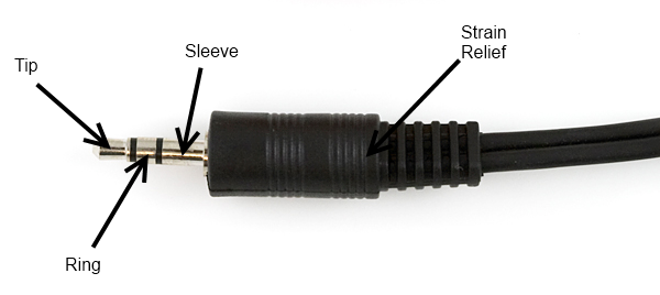
This 1/8" headphone
jack comes with a strain relief "boot" slid over the cable to prevent
forces on the cable from being transmitted directly to the electrical
joints.
USB Connectors
USB connectors come in two flavors: host and peripheral. In the USB standard, there is a difference between the two, and the connectors on cables and devices reflect this. However, all USB connectors will have some things in common:- Polarization - A USB connector can only nominally be inserted one way. It may be possible to force a connector in wrong, but that will result in damage to the device.
- Four contacts - All USB connectors have at least four contacts (although some may have five, and USB 3.0+ connectors have even more). These are for power, ground, and two data lines (D+ and D-). USB connectors are designed to transmit 5V, up to 500mA.
- Shielding - USB connectors are shielded, such that a metal shell which is not part of the electrical circuit is provided. This is important to keep the signal intact in environments with a lot of electrical "noise".
- Robust power connection - It's important for the power pins to make connection before the data lines, to avoid trying to power the device over the data lines. All USB connectors are designed with this in mind.
- Molded strain relief - All USB cables have plastic overmolding at the connector to prevent strain on the cable that could potentially damage the electrical connections.
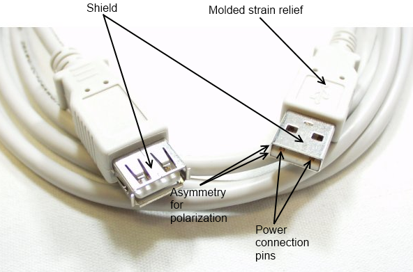
A USB extension cable, with some of the common features of USB connectors labeled.
USB-A Connectors
USB-A female is the standard "host" connector type. This is found on computers, hubs, or any device intended to have peripherals plugged into it. It is also possible to find extension cables with a female A connector and a male A connector on the other end.
Female USB-A ports on the side of a laptop. The blue connector is USB 3.0 compliant.
USB-A male is the standard "peripheral" connector
type. Most USB cables will have one end terminating in a USB-A male
connector, and many devices (such as keyboards and mice) will have a
built-in cable terminated with a USB-A male connector. It's also
possible to find USB-A male connectors that are board mountable, for
devices like USB memory sticks.
Two types of Male USB-A connectors, on a SparkFun Cerberus cable and an AVR Stick development board.
USB-B Connectors
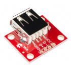
USB-B female is a standard for peripheral devices. It's bulky, but robust, so in applications where size is not an issue, it's the preferred means for providing a removable connector for USB connectivity. It is usually a through-hole board mount connector, for maximum reliability, but there are panel-mount options for it as well.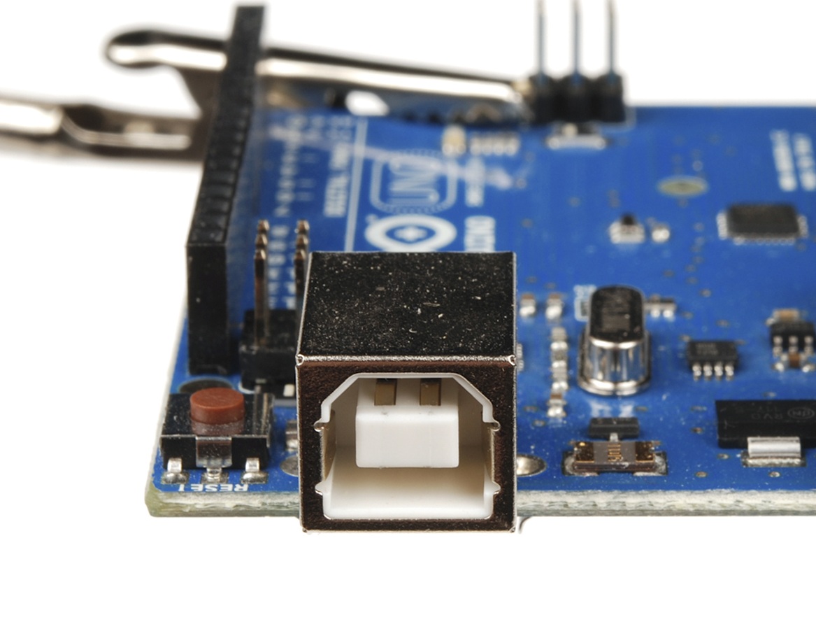
Arduino boards, including this Uno, have long used the female USB-B connector, due to its low cost and durability.
USB-B male is almost exclusively found at the end of
a cable. USB-B cables are ubiquitous and inexpensive, which also
contributes to the popularity of the USB-B connection.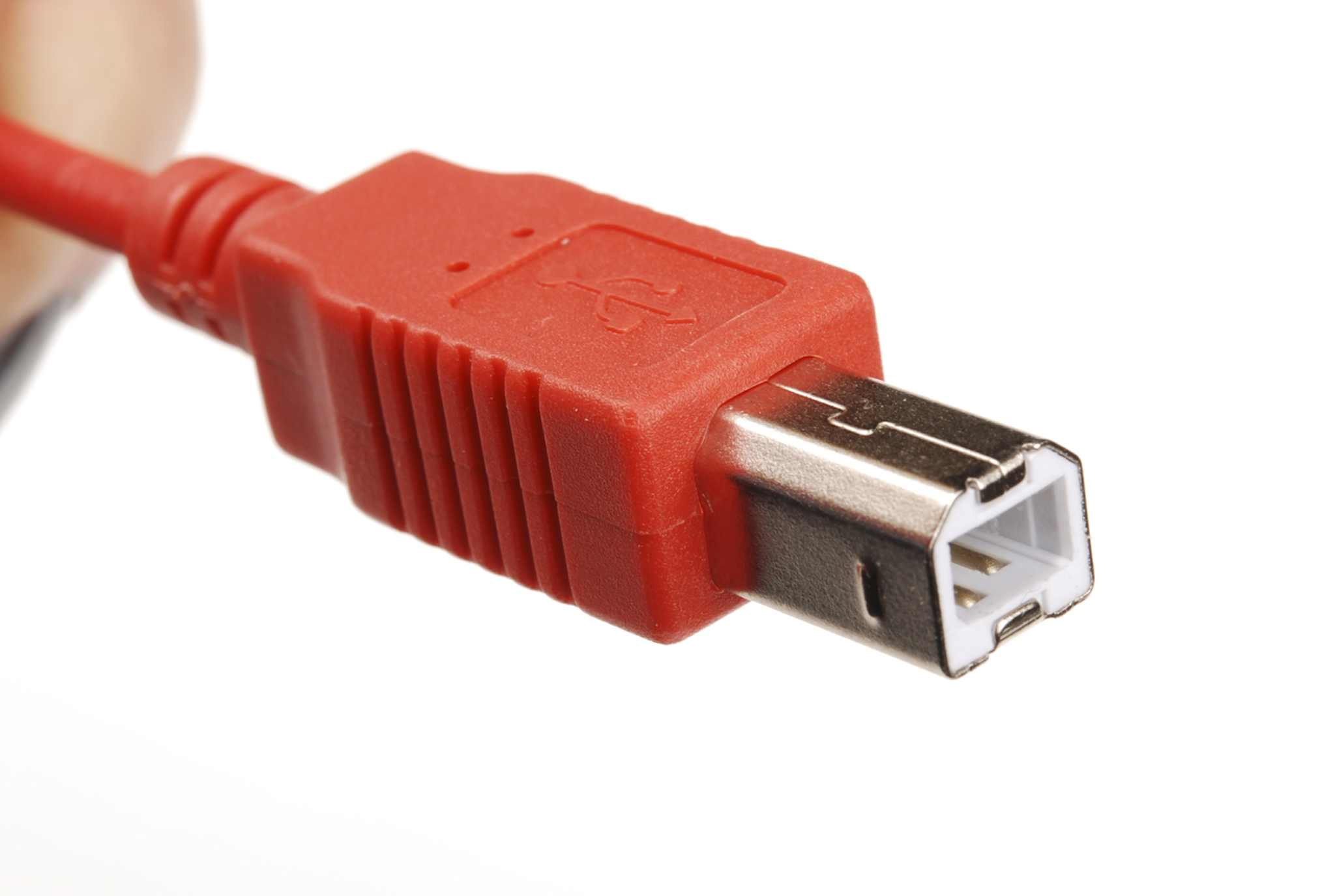
USB-B male connector on the end of a SparkFun Cerberus cable.
USB-Mini Connectors
The USB-Mini connection was the first standard attempt to reduce the size of the USB connector for smaller devices. USB-Mini female is typically found on smaller peripherals (MP3 players, older cellphones, small external hard drives), and is usually a surface mount connector, trading robustness for size. USB-Mini is slowly being phased out in favor of the USB-Micro connector.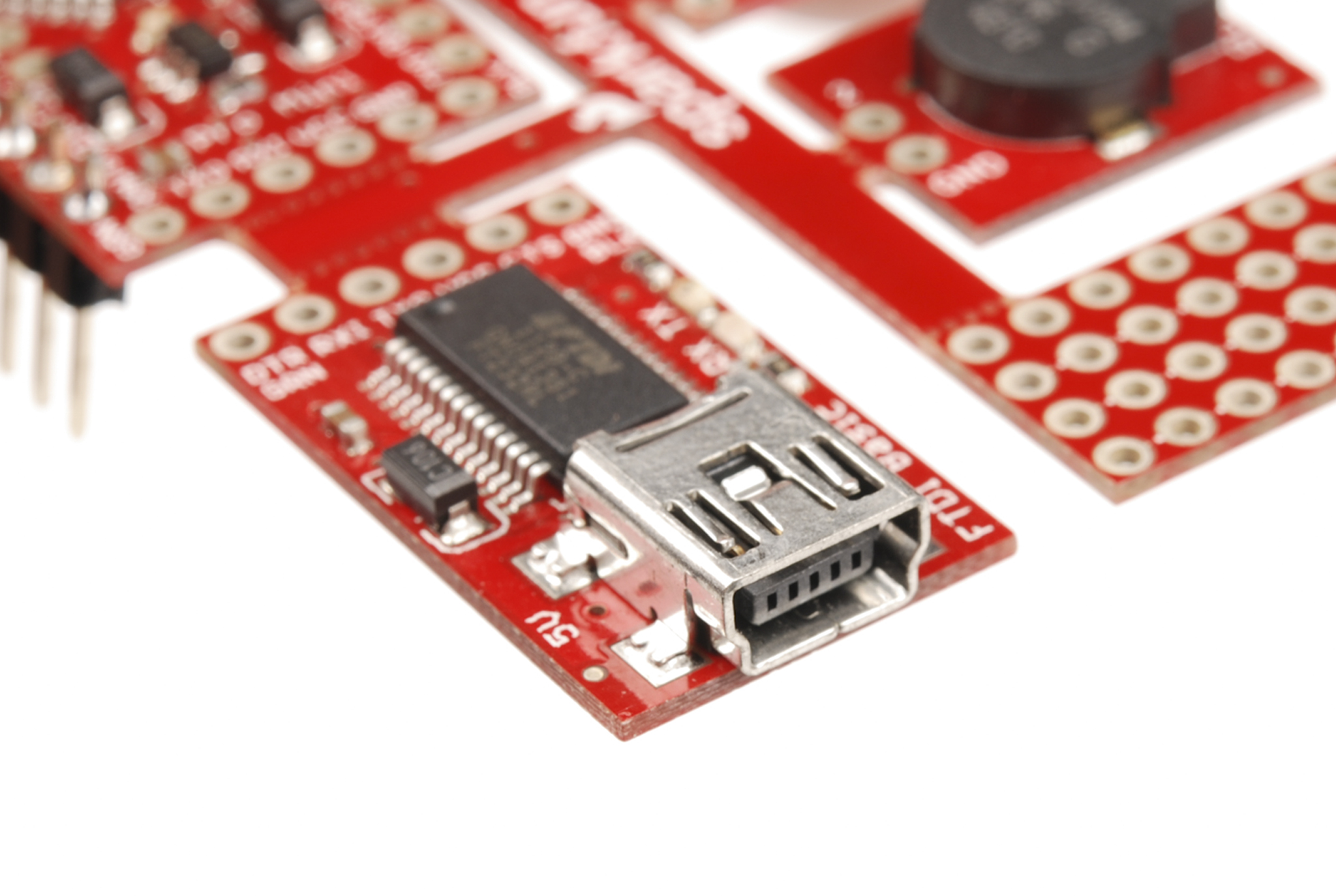
USB-Mini female connector on a Protosnap Pro Mini.
USB-Mini male is another cable-only connector. As with USB-B, it's extremely common, and cables can be found cheaply almost anywhere.
USB-Mini male connector on the end of a SparkFun Cerberus cable.
USB-Micro Connectors
USB-Micro is a fairly recent addition to the USB connector family. As with USB-Mini, the primary concern is size reduction, but USB-Micro adds a fifth pin for low-speed signalling, allowing it to be used in USB-OTG (On-the-go) applications where a device may want to operate as either a host or a peripheral depending on circumstances.USB-Micro female is found on many newer peripherals, such as digital cameras and MP3 players. The adoption of USB-micro as a standard charge port for all new cellular phones and tablet computers means that chargers and data cables are becoming increasingly common, and USB-Micro is likely to supplant USB-Mini in the coming years as the small-factor USB connector of choice.
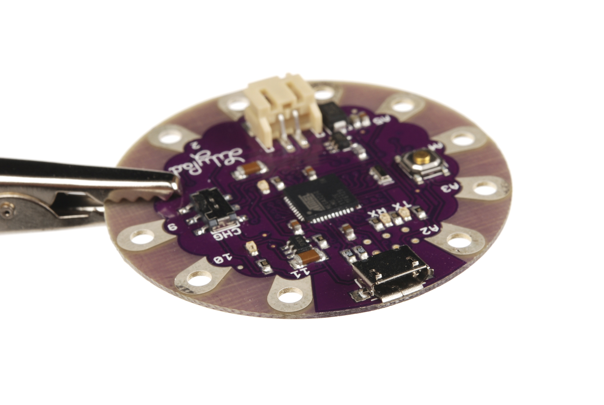
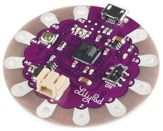
USB-Micro female connector on a LilyPad Arduino USB board.
USB-Micro male is also a cable-only connector. There
are generally two types of cables with USB-Micro male ends: one for
connecting a device with a USB-Micro port as a peripheral to a USB host
device and one for adapting the USB-Micro female port to a USB-A female
port, to be used in USB-OTG capable devices.
USB-Micro male connector on the SparkFun Cerberus cable.
Adapter pigtail
for using USB-OTG capable devices having only a USB-Micro port with
standard USB peripherals. Note that not all devices supporting USB-OTG
will work with this pigtail.
USB 3.0 micro-B Cable
USB 3.0 micro-B cables look similar to USB 2.0 micro-B connectors but they include additional pins for two differential pairs and a ground.
USB 3.1 C Cable
USB C packs 24 pins into the USB connector. Unlike the previous versions predecessors, this version is reversable! The design of the USB C cable also allows for current above 500mA for your power hungry devices.
Heads up! Depending on the cable, not all of the pins
are broken out for USB C. Some cables may be limited to the USB 2.0
specification with 4 pins as opposed to the full USB 3.1 specification.
The reversible USB A to C cables and SuzyQable
are a few examples. Depending on the USB port that is used, you may
also be limited in the amount of current that can be provided to your
device.
Reversible USB
With the advancements in technology and manufacturing, USB connectors can be inserted either way! Below are examples of a reversible type A and type micro-b connector from the catalog. |
 |
 |
 |
| Reversible Type A Connector End | Reversible Type Micro B Connector End |
If you are looking for a USB connector or cable, check out our USB Buying Guide or catalog.
Audio Connectors
Another familiar connector group are those used for audio-visual applications--RCA and phono. While these can't truly be considered to be of the same family, as the various USB connectors are, we'll consider both of them to be in the same vein."Phone" Type Connectors
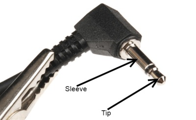
You'll probably immediately recognize the 1/8" version of this connector as a the plug on the end of a pair of headphones. These connectors actually come in three common sizes: 1/4" (6.35mm), 1/8" (3.5mm), and 2.5mm. ¼" size connectors find a lot of use in the professional audio and music community- most electric guitars and amplifiers have 1/4" tip-sleeve (TS) jacks on them. 1/8" tip-ring-sleeve (TRS) is very common as the connector for headphones or audio output signals on MP3 players or computers. Some cell phones will provide a 2.5mm tip-ring-ring-sleeve (TRRS) jack for connecting to headphones that also include a microphone for hands-free communications.The common availability of these connectors and cables makes them a good candidate for general purpose connectivity applications--for instance, long before USB, Texas Instruments graphing calculators used a 2.5mm TRS connector for a serial programming connector. It should be remembered that tip-sleeve connector types are not designed for carrying power; during insertion, the tip and the sleeve can be momentarily shorted together, which may damage the power supply. The lack of shielding makes them poor candidates for high-speed data, but low speed serial data can be passed through these connectors.
Headphone-type TRS phone plug, 1/8". Typically, tip and ring will carry the stereo audio signals while sleeve will be connected to ground.
1/8" phone plug. Note the lack of a ring contact on this connector.
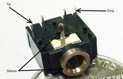
1/8" board mount headphone jack
with pins corresponding pin connections labeled. When no jack is
inserted, an internal switch connects the tip and ring pins to the
adjacent unmarked pins, allowing insertion detection.
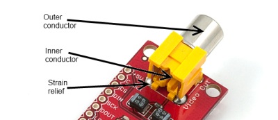
RCA Connectors
Familiar as the home-stereo connector of choice for many decades, the RCA connector was introduced in the 1940s by RCA for home phonographs. It is slowly being supplanted by connections like HDMI in the audio-visual realm, but the ubiquity of the connectors and cables makes it a good candidate for home-built systems. It will be a long time before it is obsolete.Female RCA connectors are usually found on devices, although it is possible to find extension or conversion cables with female jacks on them. Most RCA connectors are connected to one of four types of signals: component video (PAL or NTSC, depending on where the equipment was sold), composite video, stereo audio, or S/PDIF audio.
Female RCA connector, for video signals. Typically, NTSC or PAL video signal connectors will be yellow.
Male RCA connectors are usually found on cables.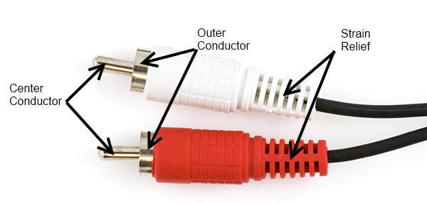
Male RCA plugs. Red and white are usually for audio applications, with red denoting the "right" audio channel.
Power Connectors
While many connectors carry power in addition to data, some connectors are used specifically to provide power connections to devices. These vary widely by application and size, but we will only focus on some of the most common ones here.Barrel Connectors
Barrel connectors are typically found on low-cost consumer electronics which can be plugged into wall power via bulky AC wall adaptors. Wall adaptors are widely available, in a variety of power ratings and voltages, making barrel connectors a common means for connecting power to small projects.The female barrel connector, or "jack", can be purchased in several varieties: PCB mounted (surface mount or through hole), cable mount, or panel mount. Some of these connectors will have an additional contact that allows the application to detect whether a power supply is plugged into the barrel jack or not, thus allowing the device to bypass batteries and save battery life when running on external power.
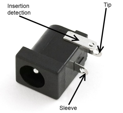
Female barrel connector. When no plug is inserted, the "insertion detection" pin will be shorted to the "sleeve" pin.
The male barrel connector, or "plug", is usually only found in a wire
termination variety, although there are multiple methods of attaching
the plug to the end of the wire. It's also possible to get plugs that
come pre-attached to a cable.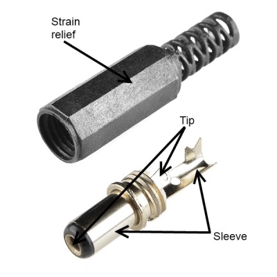
Unattached male barrel plug,
for attachment to any power supply. Note that the sleeve connection is
designed to be crimped onto the wire for extra strain relief.
Barrel connectors provide only two connections, frequently referred
to as "pin" or "tip" and "sleeve". When ordering, there are three
differentiating characteristics of a barrel connection- inner diameter
(the diameter of the pin inside the jack), outer diameter (the diameter
of the sleeve on the outside of the plug), and polarity (whether the
sleeve voltage is higher or lower than the tip voltage).Sleeve diameter is most commonly either 5.5mm or 3.5mm.
Pin diameter is contingent upon sleeve diameter; a 5.5mm sleeve will have either a 2.5mm or 2.1mm pin. Unfortunately, this means that a plug designed for a 2.5mm pin will fit in a 2.1mm jack, but that the connection will be, at best, intermittent. 3.5mm sleeve plugs usually mate to a jack with a 1.3mm pin.
Polarity is the final aspect to consider; most often, the sleeve will be considered 0V and the tip will be a positive voltage relative to the sleeve. Many devices will have a small diagram indicating the polarity expected by the device; care should be taken to adhere to this, as an improper power supply may damage the device.
Plugs of both sleeve sizes are usually 9.5mm long, but longer and shorter ones do exist. All SparkFun products use a negative 5.5mm sleeve and a positive 2.1mm pin; we recommend sticking to that standard where possible, as it seems to be the most common flavor found in the wild.
Common polarity
diagrams for AC adaptors with barrel plugs. Positive polarity (tip
positive, sleeve 0V) is most common. Diagram courtesy Wikipedia user Three-quarter-ten.
"Molex" Connectors
Most computer hard drives, optical drives, and other internal peripherals get power through what is typically called a "Molex" connector. To be more accurate, it's a Molex series 8981 connector--Molex is actually the name of the company which initially designed this connector back in the 1950s--but common usage has denuded that fact somewhat.Molex connectors are designed to carry a lot of current: up to 11A per pin. For projects where a lot of power may be needed--a CNC machine, for instance, or a 3D printer- a very common method for powering the project is to use a desktop PC power supply and connecting the various system circuits through Molex connectors.
The Molex connector is one where the male/female terminology is a bit odd. The female connector is usually found on the end of a cable, and it slips inside of a plastic shell which surrounds the male pins on the male connector. Usually, the connectors are press-fit only, and very, very tight--they are intended to be connected and disconnected only a few times and, as such, are a bad choice for systems where connections will frequently be changed.
Male Molex connector. The gender of the pins inside the connector is what signifies the gender of the connector as a whole.
Female Molex connector on a project power supply.
IEC Connector
As with the Molex connector, this is a case where a generalized component name has come to be synonymous with a single, particular item. IEC connector usually refers to the power supply inlet which is commonly seen on desktop PC power supplies. Strictly speaking, that's an IEC 60320-1 C13 (female) and C14 (male) connector.
C14 male IEC power inlet, on a DC project power supply. Note that, as with the Molex connector, the gender of the connector is defined by the pins within the hood.
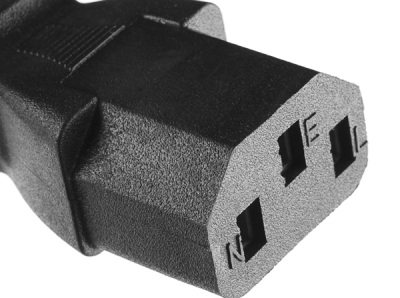
C13 female IEC power connector, on a fairly standard AC power supply cable. Cables with this end can be found all around the world, usually with the dominant local AC connector at the other end.
IEC connectors are used almost exclusively for AC power input. The
nice thing about using one on a project is that IEC-to-wall cables are
extremely common and available with localized wall plugs for most international locations!JST Connector
At SparkFun, we frequently refer to "2.0mm JST Connectors". This is yet another generalization of a specific product- JST is a Japanese company which makes high-quality connectors, and our 2.0mm JST connector of choice is the PH series two-position polarized connector.All of SparkFun's single-cell lithium-polymer ion batteries come standard with this type of JST connector, and many of our boards include this connector (or a footprint for it) as a power supply input. It has the advantage of being compact, durable, and difficult to connect backwards. Another feature, which can be an advantage or a disadvantage, depending on how you look at it, is that the JST connector is wicked hard to disconnect (although a carefully applied diagonal cutter can be helpful!) once it's mated. While this makes it unlikely to fail during use, it also means that disconnecting the battery for charging can damage the battery connector.
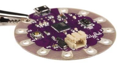
2-Pin JST male connector on a LilyPad Arduino USB board. Again, as with the Molex, the pins inside the hood determine the gender of the connector.
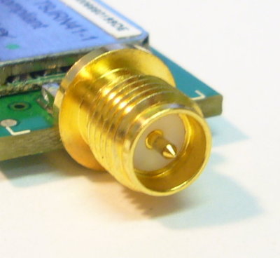
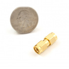
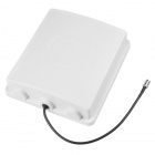
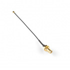
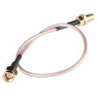
SMA Antenna Connectors
Next up is the explanation of the confusing naming conventions for SMA connectors. If you would rather not understand why the convention is the way it is, you can just look at the 4 pictures and move on. Otherwise, have fun with the read!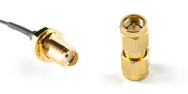
RF Connector Conventions
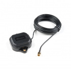
SparkFun uses SMA-type connectors on a few boards that need a 50 Ohm impedance connection to an external antenna (GPS, Bluetooth, cellular, Nordic, and XBee). However, some of these boards use different genders and polarities of the SMA connector. Therefore, we need different antennas to match the specific gender or polarity of the RF connections.There are 4 different types of SMA connectors using a combination of gender, which refers to the center pin and polarity, which refers to…..uh, this is where it gets confusing. Wikipedia tries to explain it. But from what I have found there was an original “old” design for SMA connectors.
SMA Connectors
The original SMA design called for two compliant connectors: |
 |
| SMA Male Center Pin, Inner Threads |
SMA Female Center Hole, Outer Threads |
There is one consistency however; all antennas, cables or anything was being attached to a potential stationary object used an outer nut or inner thread design and all stationary devices used the outer thread design. This applies for all SparkFun products. All of our antennas are either SMA male or RP-SMA female. All of our boards are either SMA female or RP-SMA male.
RP-SMA Connectors
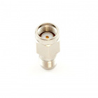
The only thing that changed with the Part 15 compliance was the center pin, thus reversing the polarity of the connection and forming a “new” standard; the reversed polarized SMA (RP-SMA). The RP (reverse polarity) is named after its “thread gender” and has an opposite-gender pin.The next two photos are considered reversed polarized (RP-SMA).
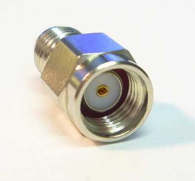 |
 |
| RP-SMA Male Center Hole, “Male” Inner Threads |
RP-SMA Female Center Pin, “Female” Outer Threads |
- Cellular and GPS (900/1700/1800MHz and 1.57542GHz respectively) generally use the old convention: SMA male for the antennas and SMA female for the modules.
- Anything 2.4GHz (Bluetooth, ZigBee, WiFi, and Nordic) generally use the new convention: RP-SMA male on the antennas and RP-SMA female on the modules.
And just in case if you happen to find the old and new mixing, we sell a SMA male to RP-SMA male and a RP-SMA female to RP-SMA male connector that will most combinations of antenna and connector to be mated.
Pin Header Connectors
Pin header connectors comprise several different means of connection. Generally, one side is a series of pins which are soldered to a PCB, and they can either be at a right-angle to the PCB surface (usually called "straight") or parallel to the board's surface (confusingly referred to as "right-angle" pins). Such connectors come in a variety of pitches, and may have any number of individual rows of pins.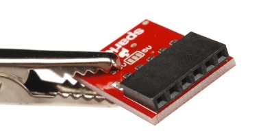
Right-angle female header pin connection on an FTDI basic board.
The most commonly seen pin headers are .1" single or double row connectors. These come in male and female
versions, and are the connectors used to connect Arduino boards and
shields together. Other pitches are not uncommon; for instance, the XBee wireless module uses a 2.0mm pitch version of the same connector.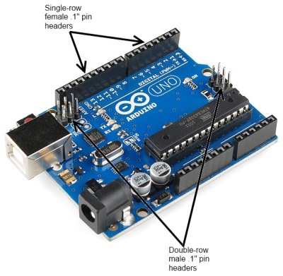
.1" pin header connectors, male and female, on an Arduino Uno board.
A common variation on this part is a "machine pin" version. While the
normal version is formed out of stamped and folded sheet metal, machine
pin connectors are formed by tooling the metal into the desired shape.
The result is a more robust connector, with a better joint and longer
life, making it somewhat more expensive.
Female machine pin headers.
Note that these are designed to be snapped apart into smaller sections,
while standard .1" female header pin connectors are not. It's also
important to note that not all non-machine pin header connectors will
mate with the machine pin variety.
Cables made to connect to these pin headers are usually one of two types: individual wires with crimp connectors on them or ribbon cables with insulation displacement
connectors. These can simply be clamped onto the end of a ribbon cable,
which creates a connection to each one of the conductors in the ribbon
cable. Generally, cables are only available as female gender and expect a
male pin to mate with.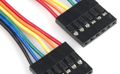
Six-position crimp-type cable. Each wire is individually stripped, a connector crimped to it, and then the connectors are inserted into the plastic frame.
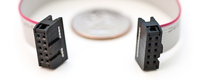
2x5 insulation displacement connectors (IDC) on a ribbon cable.
This type of cable can be quickly assembled because it does not require
stripping of individual connectors. It also has polarizing tabs on each
end, to prevent incorrect insertion in the mating board-side connector.
Temporary Connectors
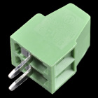
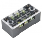
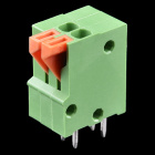
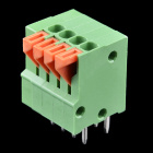
Screw Terminals
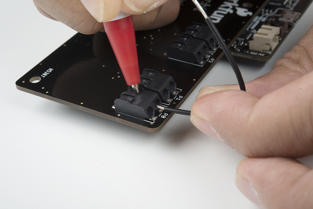
In some cases, it may be desirable to be able to connect bare, unterminated wire to a circuit. Screw terminals provide a good solution for this. They are also good for situations in which a connection should be capable of supporting multiple different connecting devices.The downside of screw terminals is that they can come undone fairly easily, leaving a bare wire waving around in your circuit. A small dab of hot glue can address this without being too difficult to remove later.
Screw terminals are typically designed for a narrow range of wire gauges, and wires that are too small can be as big a problem as wires that are too big. SparkFun carries four types of screw terminal – a 2.54mm (0.1" breadboard standard), a 3.5mm, 5mm, and 10mm pitch version.
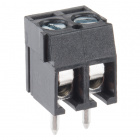
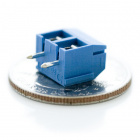
Most screw terminals are highly modular, and they can easily be
extended at the same pitch by simply connecting two or more smaller
sections together.
Spring terminals provide an alternative to screw terminals. They work better in environments with a lot of vibrations (i.e. automotive applications) or when a wire expanding/contracting due to temperature cycling. Additionally, the tension is automatically adjusted to the wire gauge (assuming it is within the accepted wire thickness) as opposed to variances in tension when a user tightens the screw terminal. Below are a few spring terminal connectors that SparkFun carries in the catalog.
Certain boards (like the gamer:bit, LumiDrive, and Qwiic MP3 Trigger to name a few) are populated with a spring terminal for easy access to I/O pins.

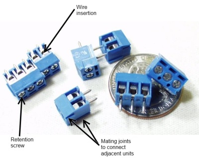
3.5mm pitch screw terminals,
showing the insertion point of the wire to be connected, the retention
screw which holds the wire in place, and the modular connectors on the
sides of the individual units allowing multiple pieces to be ganged
together.
Spring Terminals
Alternatives to screw terminals include spring terminals (a.k.a. "push-in", "cage-clamp", or "poke-home" connectors). Spring terminals work in a similar fashion as screw terminals. However, instead of tightening a screw to make a connection with piece of wire, a spring clamps together pieces of metal together.Spring terminals provide an alternative to screw terminals. They work better in environments with a lot of vibrations (i.e. automotive applications) or when a wire expanding/contracting due to temperature cycling. Additionally, the tension is automatically adjusted to the wire gauge (assuming it is within the accepted wire thickness) as opposed to variances in tension when a user tightens the screw terminal. Below are a few spring terminal connectors that SparkFun carries in the catalog.

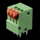
A ball-point pen pressing down on the tab of the gamer:bit's poke-home connector to connect a piece of wire.
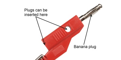
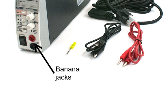
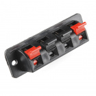
Banana Connector
Most pieces of power test equipment (multimeters, power supplies) have a very simple connector called a "banana jack" on it. These mate to "banana plugs", crimped, sprung metal plugs, meant to make a single power connection. They are frequently available in a stackable configuration and can be easily connected to any type of wire. They are capable of carrying several amps of current and are inexpensive.
Stackable banana plug. Note that there are two different ways to plug in an additional banana plug.
Extech variable bench supply with banana jacks on the front.
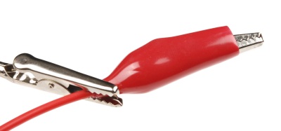
Alligator Clip
Named for obvious reasons, alligator clips are good for test connections to posts or bare wires. They tend to be bulky, easily cause shorts to nearby bare metal, and have a reasonably poor grip that can be easily compromised. They are primarily used for low-cost connections during debugging.
A "third hand" tool, which uses alligator clips to hold work pieces, holding a wire terminated with an alligator clip for electrical test. Note the plastic boot surrounding the alligator clip, to make it less likely to short to other connections.
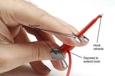
IC Clip (or IC Hook)
For more delicate probing operations, there are a variety of IC clips on the market. These are sized to allow a user to clip them onto the pins of an IC without contacting adjacent pins; some of them are delicate enough to be clipped onto even fine-pitched SMD component legs. These smaller clips can be found on logic analyzers as well as test leads, which are great for prototyping or troubleshooting circuits.
A large IC clip on the end of a wire.
This clip is still small enough to be connected to a single leg on a
through-hole chip without causing a problem for adjacent pins.
Other Connectors
RJ-type Modular Connectors
Registered jack connectors are standard for telecommunications equipment into a local exchange. The names one normally hears associated with them (RJ45, RJ12, etc) are not necessarily correct, as the RJ designator is a based on a combination of the number of positions, the number of conductors actually present, and the wiring pattern. For example, while the ends of a standard ethernet cable are usually referred to as "RJ45", RJ45 actually implies not only an 8 position, 8 conductor modular jack, it also implies that it is wired for ethernet.These modular connectors can be very useful, since they combine ready availability, multiple conductors, moderate flexibility, low cost, and moderate current carrying capacity. While not originally intended to deliver a great deal of power, these cables can be used to deliver data and a couple of hundred milliamps from one device to another. Care should be taken to ensure that jacks provided for applications like this are not connected to conventional ethernet ports, as damage will result.
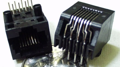
A standard 8p8c (8-position, 8-conductor) "RJ45" modular jack. Be aware that if you intend to use this type of jack to pass DC signals and power, you must avoid using connectors with built-in signal transformers.
D-sub Type Connectors
Named for the shape of their shell, D-subminiature connectors are a classic standard in the computing world. There are four very common varieties of this connector: DA-15, DB-25, DE-15, and DE-9. The pin number indicates the number of connections provided, and the letter combination indicates the size of the shell. Thus, DE-15 and DE-9 have the same shell size, but a different number of connections.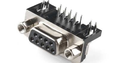
Female DE-9 board-mount connector.
Gender is defined by the pins or sockets associated with each signal,
not the connector as a whole, making this connector female despite the
fact that it effectively inserts into the shell of the mating connector.
DB-25 and DE-9 are the most useful to the hardware hacker; many
desktop computers still include at least one DE-9 serial port, and often
one DB-25 parallel port. Cables terminated with DE-9 and DB-25
connectors are widely available, too. As with the modular connector
above, these can be used to provide power and point-to-point
communications between two devices. Again, since the common usage of
these cables does not include power transmission, it is very
important that any repurposing of the cables be done cautiously, as a
non-standard device plugged into a standard port can easily cause
damage._________________________________________________________________________________
SOLDERING
PCB Basics
Overview
One of the key concepts in electronics is the printed circuit board or PCB. It's so fundamental that people often forget to explain what a PCB is. This tutorial will breakdown what makes up a PCB and some of the common terms used in the PCB world.
What's a PCB?
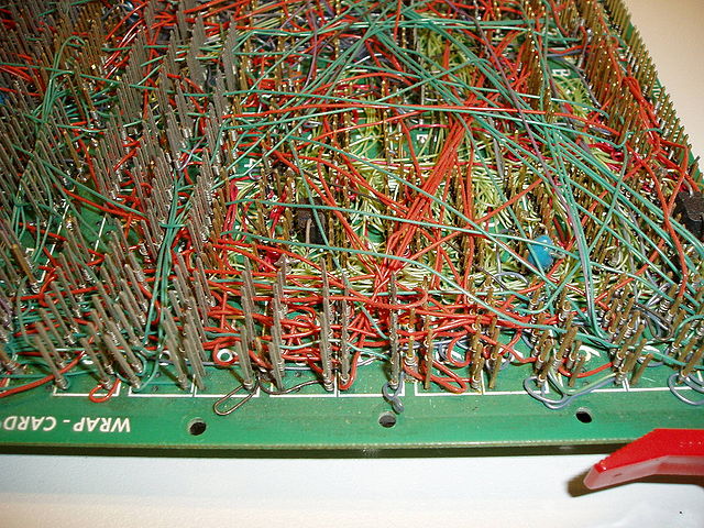
Printed circuit board is the most common name but may also be called "printed wiring boards" or "printed wiring cards". Before the advent of the PCB circuits were constructed through a laborious process of point-to-point wiring. This led to frequent failures at wire junctions and short circuits when wire insulation began to age and crack.->
courtesy Wikipedia user Wikinaut <-
A significant advance was the development of wire wrapping, where a small gauge wire is literally wrapped around a post at each connection point, creating a gas-tight connection which is highly durable and easily changeable.
As electronics moved from vacuum tubes and relays to silicon and integrated circuits, the size and cost of electronic components began to decrease. Electronics became more prevalent in consumer goods, and the pressure to reduce the size and manufacturing costs of electronic products drove manufacturers to look for better solutions. Thus was born the PCB.
Composition
A PCB is sort of like a layer cake or lasagna- there are alternating layers of different materials which are laminated together with heat and adhesive such that the result is a single object.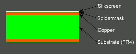
FR4
The base material, or substrate, is usually fiberglass. Historically, the most common designator for this fiberglass is "FR4". This solid core gives the PCB its rigidity and thickness. There are also flexible PCBs built on flexible high-temperature plastic (Kapton or the equivalent).You will find many different thickness PCBs; the most common thickness for SparkFun products is 1.6mm (0.063"). Some of our products- LilyPad boards and Arudino Pro Micro boards- use a 0.8mm thick board.
Copper
The next layer is a thin copper foil, which is laminated to the board with heat and adhesive. On common, double sided PCBs, copper is applied to both sides of the substrate. In lower cost electronic gadgets the PCB may have copper on only one side. When we refer to a double sided or 2-layer board we are referring to the number of copper layers (2) in our lasagna. This can be as few as 1 layer or as many as 16 layers or more.
PCB with copper exposed, no solder mask or silkscreen.
The copper thickness can vary and is specified by weight, in ounces
per square foot. The vast majority of PCBs have 1 ounce of copper per
square foot but some PCBs that handle very high power may use 2 or 3
ounce copper. Each ounce per square translates to about 35 micrometers
or 1.4 thousandths of an inch of thickness of copper.Soldermask
The layer on top of the copper foil is called the soldermask layer. This layer gives the PCB its green (or, at SparkFun, red) color. It is overlaid onto the copper layer to insulate the copper traces from accidental contact with other metal, solder, or conductive bits. This layer helps the user to solder to the correct places and prevent solder jumpers.In the example below, the green solder mask is applied to the majority of the PCB, covering up the small traces but leaving the silver rings and SMD pads exposed so they can be soldered to.
Silkscreen
The white silkscreen layer is applied on top of the soldermask layer. The silkscreen adds letters, numbers, and symbols to the PCB that allow for easier assembly and indicators for humans to better understand the board. We often use silkscreen labels to indicate what the function of each pin or LED.
Terminology
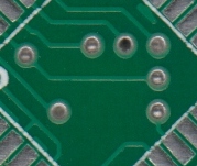
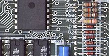
Now that you've got an idea of what a PCB structure is, let's define some terms that you may hear when dealing with PCBs:- Annular ring - the ring of copper around a plated through hole in a PCB.
Examples of annular rings.
- DRC - design rule check. A software check of your design to make sure the design does not contain errors such as traces that incorrectly touch, traces too skinny, or drill holes that are too small.
- Drill hit - places on a design where a hole should be drilled, or where they actually were drilled on the board. Inaccurate drill hits caused by dull bits are a common manufacturing issue.
Not so accurate, but functional drill hits.
- Finger - exposed metal pads along the edge of a board, used to create a connection between two circuit boards. Common examples are along the edges of computer expansion or memory boards and older cartridge-based video games.
- Mouse bites - an alternative to v-score for separating boards from panels. A number of drill hits are clustered close together, creating a weak spot where the board can be broken easily after the fact. See the SparkFun Protosnap boards for a good example.
Mouse bites on the LilyPad ProtoSnap allow the PCB to be snapped apart easily.
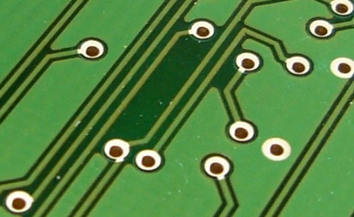
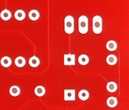
- Pad - a portion of exposed metal on the surface of a board to which a component is soldered.
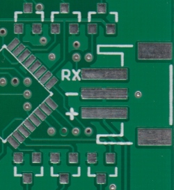
PTH (plated through-hole) pads on the left, SMD (surface mount device) pads on the right.
- Panel - a larger circuit board composed of many smaller boards which will be broken apart before use. Automated circuit board handling equipment frequently has trouble with smaller boards, and by aggregating several boards together at once, the process can be sped up significantly.
- Paste stencil - a thin, metal (or sometimes plastic) stencil which lies over the board, allowing solder paste to be deposited in specific areas during assembly.
- Plane - a continuous block of copper on a circuit board, define by borders rather than by a path. Also commonly called a "pour".
Various portions of the PCB that have no traces but has a ground pour instead.
- Plated through hole - a hole on a board which has an annular ring and which is plated all the way through the board. May be a connection point for a through hole component, a via to pass a signal through, or a mounting hole.
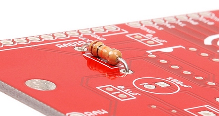
A PTH resistor inserted into the FabFM
PCB, ready to be soldered. The legs of the resistor go through the
holes. The plated holes can have traces connected to them on the front
of the PCB and the rear of the PCB.
- Pogo pin - spring-loaded contact used to make a temporary connection for test or programming purposes.
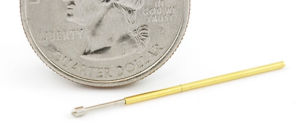
The popular pogo pin with pointed tip. We use tons of these on our test beds.
- Reflow - melting the solder to create joints between pads and component leads.
- Silkscreen - the letters, number, symbols, and imagery on a circuit board. Usually only one color is available, and resolution is usually fairly low.
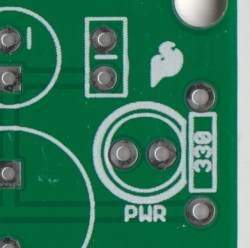
Silkscreen identifying this LED as the power LED.
- Slot - any hole in a board which is not round. Slots may or may not be plated. Slots sometimes add to add cost to the board because they require extra cut-out time.
Complex slots cut into the ProtoSnap - Pro Mini. There are also many mouse bites shown. Note: the corners of the slots cannot be made completely square because they are cut with a circular routing bit.
- Solder paste - small balls of solder suspended in a gel medium which, with the aid of a paste stencil, are applied to the surface mount pads on a PCB before the components are placed. During reflow, the solder in the paste melts, creating electrical and mechanical joints between the pads and the component.
Solder paste on a PCB shortly before the components are placed. Be sure to read about *paste stencil above as well.*
- Solder pot - a pot used to quickly hand solder boards with through hole components. Usually contains a small amount of molten solder into which the board is quickly dipped, leaving solder joints on all exposed pads.
- Soldermask - a layer of protective material laid over the metal to prevent short circuits, corrosion, and other problems. Frequently green, although other colors (SparkFun red, Arduino blue, or Apple black) are possible. Occasionally referred to as "resist".
Solder mask covers up the signal traces but leaves the pads to solder to.
- Solder jumper - a small, blob of solder connecting two adjacent pins on a component on a circuit board. Depending on the design, a solder jumper can be used to connect two pads or pins together. It can also cause unwanted shorts.
- Surface mount - construction method which allows components to be simply set on a board, not requiring that leads pass through holes in the board. This is the dominant method of assembly in use today, and allows boards to be populated quickly and easily.
- Thermal - a small trace used to connect a pad to a plane. If a pad is not thermally relieved, it becomes difficult to get the pad to a high enough temperature to create a good solder joint. An improperly thermally relieved pad will feel "sticky" when you attempt to solder to it, and will take an abnormally long time to reflow.
On the left, a solder
pad with two small traces (thermals) connecting the pin to the ground
plane. On the right, a via with no thermals connecting it completely to
the ground plane.
- Thieving - hatching, gridlines, or dots of copper left in areas of a board where no plane or traces exist. Reduces difficulty of etching because less time in the bath is required to remove unneeded copper.
- Trace - a continuous path of copper on a circuit board.
- V-score- a partial cut through a board, allowing the board to be easily snapped along a line.
- Via - a hole in a board used to pass a signal from one layer to another. Tented vias are covered by soldermask to protect them from being soldered to. Vias where connectors and components are to be attached are often untented (uncovered) so that they can be easily soldered.
Front and back of the
same PCB showing a tented via. This via brings the signal from the front
side of the PCB, through the middle of the board, to the back side.
- Wave solder - a method of soldering used on boards with through-hole components where the board is passed over a standing wave of molten solder, which adheres to exposed pads and component leads.
Designing Your Own!
How do you go about designing your own PCB? The ins and outs of PCB design are way too in depth to get into here, but if you really want to get started, here are some pointers:- Find a CAD package: there are a lot of low-cost or free options out
there on the market for PCB design. Things to consider when choosing a
package:
- Community support: are there a lot of people using the package? The more people using it, the more likely you are to find ready-made libraries with the parts you need.
- Ease-of-use: if it's painful to use it, you won't.
- Capability: some programs place limitations on your design- number of layers, number of components, size of board, etc. Most of them allow you to pay for a license to upgrade their capability.
- Portability: some free programs do not allow you to export or convert your designs, locking you in to one supplier only. Maybe that's a fair price to pay for convenience and price, maybe not.
- Look at other people's layouts to see what they have done. Open Source Hardware makes this easier than ever.
- Practice, practice, practice.
- Maintain low expectations. Your first board design will have lots of problems. Your 20th board design will have fewer, but will still have some. You'll never get rid of them all.
- Schematics are important. Trying to design a board without a good schematic in place first is an exercise in futility.
Printed circuit board
A printed circuit board (PCB) mechanically supports and electrically connects electronic components or electrical components using conductive tracks, pads and other features etched from one or more sheet layers of copper laminated onto and/or between sheet layers of a non-conductive substrate. Components are generally soldered onto the PCB to both electrically connect and mechanically fasten them to it.Printed circuit boards are used in all but the simplest electronic products. They are also used in some electrical products, such as passive switch boxes.
Alternatives to PCBs include wire wrap and point-to-point construction, both once popular but now rarely used. PCBs require additional design effort to lay out the circuit, but manufacturing and assembly can be automated. Specialized CAD software is available to do much of the work of layout. Mass-producing circuits with PCBs is cheaper and faster than with other wiring methods, as components are mounted and wired in one operation. Large numbers of PCBs can be fabricated at the same time, and the layout only has to be done once. PCBs can also be made manually in small quantities, with reduced benefits.
PCBs can be single-sided (one copper layer), double-sided (two copper layers on both sides of one substrate layer), or multi-layer (outer and inner layers of copper, alternating with layers of substrate). Multi-layer PCBs allow for much higher component density, because circuit traces on the inner layers would otherwise take up surface space between components. The rise in popularity of multilayer PCBs with more than two, and especially with more than four, copper planes was concurrent with the adoption of surface mount technology. However, multilayer PCBs make repair, analysis, and field modification of circuits much more difficult and usually impractical.
The world market for bare PCBs exceeded $60.2 billion in 2014. In 2018, the Global Single Sided Printed Circuit Board Market Analysis Report estimated that the PCB market would reach $79 billion by 2024.

A basic PCB consists of a flat sheet of insulating material and a layer of copper foil, laminated to the substrate. Chemical etching divides the copper into separate conducting lines called tracks or circuit traces, pads for connections, vias to pass connections between layers of copper, and features such as solid conductive areas for EM shielding or other purposes. The tracks function as wires fixed in place, and are insulated from each other by air and the board substrate material. The surface of a PCB may have a coating that protects the copper from corrosion and reduces the chances of solder shorts between traces or undesired electrical contact with stray bare wires. For its function in helping to prevent solder shorts, the coating is called solder resist.
A printed circuit board can have multiple copper layers. A two-layer board has copper on both sides; multi layer boards sandwich additional copper layers between layers of insulating material. Conductors on different layers are connected with vias, which are copper-plated holes that function as electrical tunnels through the insulating substrate. Through-hole component leads sometimes also effectively function as vias. After two-layer PCBs, the next step up is usually four-layer. Often two layers are dedicated as power supply and ground planes, and the other two are used for signal wiring between components.
"Through hole" components are mounted by their wire leads passing through the board and soldered to traces on the other side. "Surface mount" components are attached by their leads to copper traces on the same side of the board. A board may use both methods for mounting components. PCBs with only through-hole mounted components are now uncommon. Surface mounting is used for transistors, diodes, IC chips, resistors and capacitors. Through-hole mounting may be used for some large components such as electrolytic capacitors and connectors.
The pattern to be etched into each copper layer of a PCB is called the "artwork". The etching is usually done using photoresist which is coated onto the PCB, then exposed to light projected in the pattern of the artwork. The resist material protects the copper from dissolution into the etching solution. The etched board is then cleaned. A PCB design can be mass-reproduced in a way similar to the way photographs can be mass-duplicated from film negatives using a photographic printer.
In multi-layer boards, the layers of material are laminated together in an alternating sandwich: copper, substrate, copper, substrate, copper, etc.; each plane of copper is etched, and any internal vias (that will not extend to both outer surfaces of the finished multilayer board) are plated-through, before the layers are laminated together. Only the outer layers need be coated; the inner copper layers are protected by the adjacent substrate layers.
FR-4 glass epoxy is the most common insulating substrate. Another substrate material is cotton paper impregnated with phenolic resin, often tan or brown.
When a PCB has no components installed, it is less ambiguously called a printed wiring board (PWB) or etched wiring board. However, the term "printed wiring board" has fallen into disuse. A PCB populated with electronic components is called a printed circuit assembly (PCA), printed circuit board assembly or PCB assembly (PCBA). In informal usage, the term "printed circuit board" most commonly means "printed circuit assembly" (with components). The IPC preferred term for assembled boards is circuit card assembly (CCA), and for assembled backplanes it is backplane assemblies. "Card" is another widely used informal term for a "printed circuit assembly". For example, expansion card.
A PCB may be "silkscreen" printed with a legend identifying the components, test points, or identifying text. Originally, an actual silkscreen printing process was used for this purpose, but today other, finer quality printing methods are usually used instead. Normally the screen printing is not significant to the function of the PCBA.
A minimal PCB for a single component, used for prototyping, is called a breakout board. The purpose of a breakout board is to "break out" the leads of a component on separate terminals so that manual connections to them can be made easily. Breakout boards are especially used for surface-mount components or any components with fine lead pitch.
Advanced PCBs may contain components embedded in the substrate
Characteristics
Through-hole technology
.jpg)
Through-hole (leaded) resistors
Through-hole manufacture adds to board cost by requiring many holes to be drilled accurately, and it limits the available routing area for signal traces on layers immediately below the top layer on multi-layer boards, since the holes must pass through all layers to the opposite side. Once surface-mounting came into use, small-sized SMD components were used where possible, with through-hole mounting only of components unsuitably large for surface-mounting due to power requirements or mechanical limitations, or subject to mechanical stress which might damage the PCB (e.g. by lifting the copper off the board surface).
 Through-hole devices mounted on the circuit board of a mid-1980s Commodore 64 home computer
 A box of drill bits used for making holes in printed circuit boards. While tungsten-carbide bits are very hard, they eventually wear out or break. Drilling is a considerable part of the cost of a through-hole printed circuit board.


Surface-mount technology

Surface mount components, including resistors, transistors and an integrated circuit

A PCB in a computer mouse: the component side (left) and the printed side (right)
Circuit properties of the PCB
Each trace consists of a flat, narrow part of the copper foil that remains after etching. Its resistance, determined by its width, thickness, and length, must be sufficiently low for the current the conductor will carry. Power and ground traces may need to be wider than signal traces. In a multi-layer board one entire layer may be mostly solid copper to act as a ground plane for shielding and power return. For microwave circuits, transmission lines can be laid out in a planar form such as stripline or microstrip with carefully controlled dimensions to assure a consistent impedance. In radio-frequency and fast switching circuits the inductance and capacitance of the printed circuit board conductors become significant circuit elements, usually undesired; conversely, they can be used as a deliberate part of the circuit design, as in distributed element filters, antennae, and fuses, obviating the need for additional discrete components.Materials
RoHS compliant PCB
The European Union bans the use of lead (among other heavy metals) in consumer items, a piece of legislature called the RoHS, for Restriction of Hazardous Substances, directive. PCBs to be sold in the EU must be RoHS-compliant, meaning that all manufacturing processes must not involve the use of lead, all solder used must be lead-free, and all components mounted on the board must be free of lead, mercury, cadmium, and other heavy metals.Laminates
Laminates are manufactured by curing under pressure and temperature layers of cloth or paper with thermoset resin to form an integral final piece of uniform thickness. The size can be up to 4 by 8 feet (1.2 by 2.4 m) in width and length. Varying cloth weaves (threads per inch or cm), cloth thickness, and resin percentage are used to achieve the desired final thickness and dielectric characteristics. Available standard laminate thickness are listed in ANSI/IPC-D-275.The cloth or fiber material used, resin material, and the cloth to resin ratio determine the laminate's type designation (FR-4, CEM-1, G-10, etc.) and therefore the characteristics of the laminate produced. Important characteristics are the level to which the laminate is fire retardant, the dielectric constant (er), the loss factor (tδ), the tensile strength, the shear strength, the glass transition temperature (Tg), and the Z-axis expansion coefficient (how much the thickness changes with temperature).
There are quite a few different dielectrics that can be chosen to provide different insulating values depending on the requirements of the circuit. Some of these dielectrics are polytetrafluoroethylene (Teflon), FR-4, FR-1, CEM-1 or CEM-3. Well known pre-preg materials used in the PCB industry are FR-2 (phenolic cotton paper), FR-3 (cotton paper and epoxy), FR-4 (woven glass and epoxy), FR-5 (woven glass and epoxy), FR-6 (matte glass and polyester), G-10 (woven glass and epoxy), CEM-1 (cotton paper and epoxy), CEM-2 (cotton paper and epoxy), CEM-3 (non-woven glass and epoxy), CEM-4 (woven glass and epoxy), CEM-5 (woven glass and polyester). Thermal expansion is an important consideration especially with ball grid array (BGA) and naked die technologies, and glass fiber offers the best dimensional stability.
FR-4 is by far the most common material used today. The board stock with unetched copper on it is called "copper-clad laminate".
With decreasing size of board features and increasing frequencies, small nonhomogeneities like uneven distribution of fiberglass or other filler, thickness variations, and bubbles in the resin matrix, and the associated local variations in the dielectric constant, are gaining importance.
Key substrate parameters
The circuitboard substrates are usually dielectric composite materials. The composites contain a matrix (usually an epoxy resin) and a reinforcement (usually a woven, sometimes nonwoven, glass fibers, sometimes even paper), and in some cases a filler is added to the resin (e.g. ceramics; titanate ceramics can be used to increase the dielectric constant).The reinforcement type defines two major classes of materials: woven and non-woven. Woven reinforcements are cheaper, but the high dielectric constant of glass may not be favorable for many higher-frequency applications. The spatially nonhomogeneous structure also introduces local variations in electrical parameters, due to different resin/glass ratio at different areas of the weave pattern. Nonwoven reinforcements, or materials with low or no reinforcement, are more expensive but more suitable for some RF/analog applications.
The substrates are characterized by several key parameters, chiefly thermomechanical (glass transition temperature, tensile strength, shear strength, thermal expansion), electrical (dielectric constant, loss tangent, dielectric breakdown voltage, leakage current, tracking resistance...), and others (e.g. moisture absorption).
At the glass transition temperature the resin in the composite softens and significantly increases thermal expansion; exceeding Tg then exerts mechanical overload on the board components - e.g. the joints and the vias. Below Tg the thermal expansion of the resin roughly matches copper and glass, above it gets significantly higher. As the reinforcement and copper confine the board along the plane, virtually all volume expansion projects to the thickness and stresses the plated-through holes. Repeated soldering or other exposition to higher temperatures can cause failure of the plating, especially with thicker boards; thick boards therefore require a matrix with a high Tg.
The materials used determine the substrate's dielectric constant. This constant is also dependent on frequency, usually decreasing with frequency. As this constant determines the signal propagation speed, frequency dependence introduces phase distortion in wideband applications; as flat a dielectric constant vs frequency characteristics as is achievable is important here. The impedance of transmission lines decreases with frequency, therefore faster edges of signals reflect more than slower ones.
Dielectric breakdown voltage determines the maximum voltage gradient the material can be subjected to before suffering a breakdown (conduction, or arcing, through the dielectric).
Tracking resistance determines how the material resists high voltage electrical discharges creeping over the board surface.
Loss tangent determines how much of the electromagnetic energy from the signals in the conductors is absorbed in the board material. This factor is important for high frequencies. Low-loss materials are more expensive. Choosing unnecessarily low-loss material is a common engineering error in high-frequency digital design; it increases the cost of the boards without a corresponding benefit. Signal degradation by loss tangent and dielectric constant can be easily assessed by an eye pattern.
Moisture absorption occurs when the material is exposed to high humidity or water. Both the resin and the reinforcement may absorb water; water also may be soaked by capillary forces through voids in the materials and along the reinforcement. Epoxies of the FR-4 materials aren't too susceptible, with absorption of only 0.15%. Teflon has very low absorption of 0.01%. Polyimides and cyanate esters, on the other side, suffer from high water absorption. Absorbed water can lead to significant degradation of key parameters; it impairs tracking resistance, breakdown voltage, and dielectric parameters. Relative dielectric constant of water is about 73, compared to about 4 for common circuit board materials. Absorbed moisture can also vaporize on heating, as during soldering, and cause cracking and delamination, the same effect responsible for "popcorning" damage on wet packaging of electronic parts. Careful baking of the substrates may be required to dry them prior to soldering.
Common substrates
Often encountered materials:- FR-2, phenolic paper or phenolic cotton paper, paper impregnated with a phenol formaldehyde resin. Common in consumer electronics with single-sided boards. Electrical properties inferior to FR-4. Poor arc resistance. Generally rated to 105 °C.
- FR-4, a woven fiberglass cloth impregnated with an epoxy resin. Low water absorption (up to about 0.15%), good insulation properties, good arc resistance. Very common. Several grades with somewhat different properties are available. Typically rated to 130 °C.
- Aluminum, or metal core board or insulated metal substrate (IMS), clad with thermally conductive thin dielectric - used for parts requiring significant cooling - power switches, LEDs. Consists of usually single, sometimes double layer thin circuit board based on e.g. FR-4, laminated on aluminum sheet metal, commonly 0.8, 1, 1.5, 2 or 3 mm thick. The thicker laminates sometimes also come with thicker copper metalization.
- Flexible substrates - can be a standalone copper-clad foil or can be laminated to a thin stiffener, e.g. 50-130 µm
- Kapton or UPILEX, a polyimide foil. Used for flexible printed circuits, in this form common in small form-factor consumer electronics or for flexible interconnects. Resistant to high temperatures.
- Pyralux, a polyimide-fluoropolymer composite foil. Copper layer can delaminate during soldering.
- FR-1, like FR-2, typically specified to 105 °C, some grades rated to 130 °C. Room-temperature punchable. Similar to cardboard. Poor moisture resistance. Low arc resistance.
- FR-3, cotton paper impregnated with epoxy. Typically rated to 105 °C.
- FR-5, woven fiberglass and epoxy, high strength at higher temperatures, typically specified to 170 °C.
- FR-6, matte glass and polyester
- G-10, woven glass and epoxy - high insulation resistance, low moisture absorption, very high bond strength. Typically rated to 130 °C.
- G-11, woven glass and epoxy - high resistance to solvents, high flexural strength retention at high temperatures. Typically rated to 170 °C.
- CEM-1, cotton paper and epoxy
- CEM-2, cotton paper and epoxy
- CEM-3, non-woven glass and epoxy
- CEM-4, woven glass and epoxy
- CEM-5, woven glass and polyester
- PTFE, ("Teflon") - expensive, low dielectric loss, for high frequency applications, very low moisture absorption (0.01%), mechanically soft. Difficult to laminate, rarely used in multilayer applications.
- PTFE, ceramic filled - expensive, low dielectric loss, for high frequency applications. Varying ceramics/PTFE ratio allows adjusting dielectric constant and thermal expansion.
- RF-35, fiberglass-reinforced ceramics-filled PTFE. Relatively less expensive, good mechanical properties, good high-frequency properties.
- Alumina, a ceramic. Hard, brittle, very expensive, very high performance, good thermal conductivity.
- Polyimide, a high-temperature polymer. Expensive, high-performance. Higher water absorption (0.4%). Can be used from cryogenic temperatures to over 260 °C.
Copper thickness
Copper thickness of PCBs can be specified directly or as the weight of copper per area (in ounce per square foot) which is easier to measure. One ounce per square foot is 1.344 mils or 34 micrometers thickness. Heavy copper is a layer exceeding three ounces of copper per ft2, or approximately 0.0042 inches (4.2 mils, 105 μm) thick. Heavy copper layers are used for high current or to help dissipate heat.On the common FR-4 substrates, 1 oz copper per ft2 (35 µm) is the most common thickness; 2 oz (70 µm) and 0.5 oz (18 µm) thickness is often an option. Less common are 12 and 105 µm, 9 µm is sometimes available on some substrates. Flexible substrates typically have thinner metalization. Metal-core boards for high power devices commonly use thicker copper; 35 µm is usual but also 140 and 400 µm can be encountered.
Safety certification (US)
Safety Standard UL 796 covers component safety requirements for printed wiring boards for use as components in devices or appliances. Testing analyzes characteristics such as flammability, maximum operating temperature, electrical tracking, heat deflection, and direct support of live electrical parts.Design

A board designed in 1967; the sweeping curves in the traces are evidence of freehand design using adhesive tape
Modern PCBs are designed with dedicated layout software, generally in the following steps:
- Schematic capture through an electronic design automation (EDA) tool.
- Card dimensions and template are decided based on required circuitry and case of the PCB.
- The positions of the components and heat sinks are determined.
- Layer stack of the PCB is decided, with one to tens of layers depending on complexity. Ground and power planes are decided. A power plane is the counterpart to a ground plane and behaves as an AC signal ground while providing DC power to the circuits mounted on the PCB. Signal interconnections are traced on signal planes. Signal planes can be on the outer as well as inner layers. For optimal EMI performance high frequency signals are routed in internal layers between power or ground planes.
- Line impedance is determined using dielectric layer thickness, routing copper thickness and trace-width. Trace separation is also taken into account in case of differential signals. Microstrip, stripline or dual stripline can be used to route signals.
- Components are placed. Thermal considerations and geometry are taken into account. Vias and lands are marked.
- Signal traces are routed. Electronic design automation tools usually create clearances and connections in power and ground planes automatically.
- Gerber files are generated for manufacturing.
Manufacturing
PCB manufacturing consists of many steps.PCB CAM
Manufacturing starts from the fabrication data generated by computer aided design, and component information. The fabrication data is read into the CAM (Computer Aided Manufacturing) software. CAM performs the following functions:- Input of the fabrication data.
- Verification of the data
- Compensation for deviations in the manufacturing processes (e.g. scaling to compensate for distortions during lamination)
- Panelization
- Output of the digital tools (copper patterns, drill files, inspection, and others)
Panelization
Several small printed circuit boards can be grouped together for processing as a panel. A panel consisting of a design duplicated n-times is also called an n-panel, whereas a multi-panel combines several different design onto a single panel. The outer tooling strip often includes tooling holes, a set of panel fiducials, a test coupon, and may include hatched copper pour or similar patterns for even copper distribution over the whole panel in order to avoid bending. The assemblers often mount components on panels rather than single PCBs because this is efficient. Panelization may also be necessary for boards with components placed near an edge of the board because otherwise the board could not be mounted during assembly. Most assembly shops require a free area of at least 10 mm around the board.The panel is eventually broken into individual PCBs along perforations or grooves in the panel through milling or cutting. For milled panels a common distance between the individual boards is 2 to 3 mm. Today depaneling is often done by lasers which cut the board with no contact. Laser depaneling reduces stress on the fragile circuits, improving the yield of defect-free units.
Copper patterning
The first step is to replicate the pattern in the fabricator's CAM system on a protective mask on the copper foil PCB layers. Subsequent etching removes the unwanted copper. (Alternatively, a conductive ink can be ink-jetted on a blank (non-conductive) board. This technique is also used in the manufacture of hybrid circuits.)- Silk screen printing uses etch-resistant inks to create the protective mask.
- Photoengraving uses a photomask and developer to selectively remove a UV-sensitive photoresist coating and thus create a photoresist mask. Direct imaging techniques are sometimes used for high-resolution requirements. Experiments were made with thermal resist.
- PCB milling uses a two or three-axis mechanical milling system to mill away the copper foil from the substrate. A PCB milling machine (referred to as a 'PCB Prototyper') operates in a similar way to a plotter, receiving commands from the host software that control the position of the milling head in the x, y, and (if relevant) z axis.
- Laser resist ablation Spray black paint onto copper clad laminate, place into CNC laser plotter. The laser raster-scans the PCB and ablates (vaporizes) the paint where no resist is wanted. (Note: laser copper ablation is rarely used and is considered experimental.)
- Laser etching The copper may be removed directly by a CNC laser. Like PCB milling above this is used mainly for prototyping.
Large volume
- Silk screen printing – Used for PCBs with bigger features
- Photoengraving – Used when finer features are required
Small volume
- Print onto transparent film and use as photo mask along with photo-sensitized boards, then etch. (Alternatively, use a film photoplotter)
- Laser resist ablation
- PCB milling
- Laser etching
Hobbyist
- Laser-printed resist: Laser-print onto toner transfer paper, heat-transfer with an iron or modified laminator onto bare laminate, soak in water bath, touch up with a marker, then etch.
- Vinyl film and resist, non-washable marker, some other methods. Labor-intensive, only suitable for single boards.
Subtractive, additive and semi-additive processes

The two processing methods used to produce a double-sided PWB with plated-through holes
Semi-additive is the most common process: The unpatterned board has a thin layer of copper already on it. A reverse mask is then applied. (Unlike a subtractive process mask, this mask exposes those parts of the substrate that will eventually become the traces.) Additional copper is then plated onto the board in the unmasked areas; copper may be plated to any desired weight. Tin-lead or other surface platings are then applied. The mask is stripped away and a brief etching step removes the now-exposed bare original copper laminate from the board, isolating the individual traces. Some single-sided boards which have plated-through holes are made in this way. General Electric made consumer radio sets in the late 1960s using additive boards.
The (semi-)additive process is commonly used for multi-layer boards as it facilitates the plating-through of the holes to produce conductive vias in the circuit board.

PCB copper electroplating line in the process of pattern plating copper

PCBs in process of having copper pattern plated (note the blue dry film resist)
Chemical etching
Chemical etching is usually done with ammonium persulfate or ferric chloride. For PTH (plated-through holes), additional steps of electroless deposition are done after the holes are drilled, then copper is electroplated to build up the thickness, the boards are screened, and plated with tin/lead. The tin/lead becomes the resist leaving the bare copper to be etched away.The simplest method, used for small-scale production and often by hobbyists, is immersion etching, in which the board is submerged in etching solution such as ferric chloride. Compared with methods used for mass production, the etching time is long. Heat and agitation can be applied to the bath to speed the etching rate. In bubble etching, air is passed through the etchant bath to agitate the solution and speed up etching. Splash etching uses a motor-driven paddle to splash boards with etchant; the process has become commercially obsolete since it is not as fast as spray etching. In spray etching, the etchant solution is distributed over the boards by nozzles, and recirculated by pumps. Adjustment of the nozzle pattern, flow rate, temperature, and etchant composition gives predictable control of etching rates and high production rates.
As more copper is consumed from the boards, the etchant becomes saturated and less effective; different etchants have different capacities for copper, with some as high as 150 grams of copper per litre of solution. In commercial use, etchants can be regenerated to restore their activity, and the dissolved copper recovered and sold. Small-scale etching requires attention to disposal of used etchant, which is corrosive and toxic due to its metal content.
The etchant removes copper on all surfaces not protected by the resist. "Undercut" occurs when etchant attacks the thin edge of copper under the resist; this can reduce conductor widths and cause open-circuits. Careful control of etch time is required to prevent undercut. Where metallic plating is used as a resist, it can "overhang" which can cause short-circuits between adjacent traces when closely spaced. Overhang can be removed by wire-brushing the board after etching.
Lamination

Cut through a SDRAM-module, a multi-layer PCB. Note the via, visible as a bright copper-colored band running between the top and bottom layers of the board.
The inner layers are given a complete machine inspection before lamination because mistakes cannot be corrected afterwards. The automatic optical inspection system compares an image of the board with the digital image generated from the original design data. Automated Optical Shaping (AOS) machines can then add missing copper or remove excess copper using a laser, reducing the number of PCBs that have to be discarded. PCB tracks can have a width of just 10 micrometers.
Drilling

Eyelets (hollow)
Holes may be made conductive, by electroplating or inserting hollow metal eyelets, to connect board layers. Some conductive holes are intended for the insertion of through-hole-component leads. Others used to connect board layers, are called vias.
When vias with a diameter smaller than 76.2 micrometers are required, drilling with mechanical bits is impossible because of high rates of wear and breakage. In this case, the vias may be laser drilled—evaporated by lasers. Laser-drilled vias typically have an inferior surface finish inside the hole. These holes are called micro vias and can have diameters as small as 10 micrometers. It is also possible with controlled-depth drilling, laser drilling, or by pre-drilling the individual sheets of the PCB before lamination, to produce holes that connect only some of the copper layers, rather than passing through the entire board. These holes are called blind vias when they connect an internal copper layer to an outer layer, or buried vias when they connect two or more internal copper layers and no outer layers. Laser drilling machines can drill thousands of holes per second and can use either UV or CO2 lasers.
The hole walls for boards with two or more layers can be made conductive and then electroplated with copper to form plated-through holes. These holes electrically connect the conducting layers of the PCB. For multi-layer boards, those with three layers or more, drilling typically produces a smear of the high temperature decomposition products of bonding agent in the laminate system. Before the holes can be plated through, this smear must be removed by a chemical de-smear process, or by plasma-etch. The de-smear process ensures that a good connection is made to the copper layers when the hole is plated through. On high reliability boards a process called etch-back is performed chemically with a potassium permanganate based etchant or plasma. The etch-back removes resin and the glass fibers so that the copper layers extend into the hole and as the hole is plated become integral with the deposited copper.
Plating and coating
Proper plating or surface finish selection can be critical to process yield, the amount of rework, field failure rate, and reliability.PCBs are plated with solder, tin, or gold over nickel and a resist for etching away the unneeded underlying copper.
After PCBs are etched and then rinsed with water, the solder mask is applied, and then any exposed copper is coated with solder, nickel/gold, or some other anti-corrosion coating.
Matte solder is usually fused to provide a better bonding surface for bare copper. Treatments, such as benzimidazolethiol, prevent surface oxidation of bare copper. The places to which components will be mounted are typically plated, because untreated bare copper oxidizes quickly, and therefore is not readily solderable. Traditionally, any exposed copper was coated with solder by hot air solder levelling (HASL). The HASL finish prevents oxidation from the underlying copper, thereby guaranteeing a solderable surface. This solder was a tin-lead alloy, however new solder compounds are now used to achieve compliance with the RoHS directive in the EU, which restricts the use of lead. One of these lead-free compounds is SN100CL, made up of 99.3% tin, 0.7% copper, 0.05% nickel, and a nominal of 60 ppm germanium.
It is important to use solder compatible with both the PCB and the parts used. An example is ball grid array (BGA) using tin-lead solder balls for connections losing their balls on bare copper traces or using lead-free solder paste.
Other platings used are OSP (organic surface protectant), immersion silver (IAg), immersion tin, electroless nickel with immersion gold coating (ENIG), electroless nickel electroless palladium immersion gold (ENEPIG) and direct gold plating (over copper). Edge connectors, placed along one edge of some boards, are often nickel-plated then gold-plated. Another coating consideration is rapid diffusion of coating metal into tin solder. Tin forms intermetallics such as Cu6Sn5 and Ag3Cu that dissolve into the Tin liquidus or solidus (at 50 °C), stripping surface coating or leaving voids.
Electrochemical migration (ECM) is the growth of conductive metal filaments on or in a printed circuit board (PCB) under the influence of a DC voltage bias. Silver, zinc, and aluminum are known to grow whiskers under the influence of an electric field. Silver also grows conducting surface paths in the presence of halide and other ions, making it a poor choice for electronics use. Tin will grow "whiskers" due to tension in the plated surface. Tin-lead or solder plating also grows whiskers, only reduced by reducing the percentage of tin. Reflow to melt solder or tin plate to relieve surface stress lowers whisker incidence. Another coating issue is tin pest, the transformation of tin to a powdery allotrope at low temperature.
Solder resist application
Areas that should not be soldered may be covered with solder resist (solder mask). One of the most common solder resists used today is called "LPI" (liquid photoimageable solder mask). A photo-sensitive coating is applied to the surface of the PWB, then exposed to light through the solder mask image film, and finally developed where the unexposed areas are washed away. Dry film solder mask is similar to the dry film used to image the PWB for plating or etching. After being laminated to the PWB surface it is imaged and developed as LPI. Once but no longer commonly used, because of its low accuracy and resolution, is to screen print epoxy ink. In addition to repelling solder, solder resist also provides protection from the environment to the copper that would otherwise be exposed.Silkscreen printing
A legend is often printed on one or both sides of the PCB. It contains the component designators, switch settings, test points and other indications helpful in assembling, testing, servicing, and sometimes using the circuit board.There are three methods to print the legend.
- Silk screen printing epoxy ink was the established method. It was so common that legend is often misnamed silk or silkscreen.
- Liquid photo imaging is a more accurate method than screen printing.
- Ink jet printing is new but increasingly used. Ink jet can print variable data, unique to each PWB unit, such as text or a bar code with a serial number.
Bare-board test
Boards with no components installed are usually bare-board tested for "shorts" and "opens". A short is a connection between two points that should not be connected. An open is a missing connection between points that should be connected. For high-volume production, a fixture or a rigid needle adapter makes contact with copper lands on the board. The fixture or adapter is a significant fixed cost and this method is only economical for high-volume or high-value production. For small or medium volume production flying probe testers are used where test probes are moved over the board by an XY drive to make contact with the copper lands. There is no need for a fixture and hence the fixed costs are much lower. The CAM system instructs the electrical tester to apply a voltage to each contact point as required and to check that this voltage appears on the appropriate contact points and only on these.Assembly

PCB with test connection pads
There are a variety of soldering techniques used to attach components to a PCB. High volume production is usually done with a "Pick and place machine" or SMT placement machine and bulk wave soldering or reflow ovens, but skilled technicians are able to hand-solder very tiny parts (for instance 0201 packages which are 0.02 in. by 0.01 in.) under a microscope, using tweezers and a fine-tip soldering iron, for small volume prototypes. Some SMT parts cannot be soldered by hand, such as BGA packages. All through-hole components can be hand soldered, making them favored for prototyping where size, weight, and the use of the exact components that would be used in high volume production are not concerns.
Often, through-hole and surface-mount construction must be combined in a single assembly because some required components are available only in surface-mount packages, while others are available only in through-hole packages. Or, even if all components are available in through-hole packages, it might be desired to take advantage of the size, weight, and cost reductions obtainable by using some available surface-mount devices. Another reason to use both methods is that through-hole mounting can provide needed strength for components likely to endure physical stress (such as connectors that are frequently mated and demated or that connect to cables expected to impart substantial stress to the PCB-and-connector interface), while components that are expected to go untouched will take up less space using surface-mount techniques. For further comparison, see the SMT page.
After the board has been populated it may be tested in a variety of ways:
- While the power is off, visual inspection, automated optical inspection. JEDEC guidelines for PCB component placement, soldering, and inspection are commonly used to maintain quality control in this stage of PCB manufacturing.
- While the power is off, analog signature analysis, power-off testing.
- While the power is on, in-circuit test, where physical measurements (for example, voltage) can be done.
- While the power is on, functional test, just checking if the PCB does what it had been designed to do.
In boundary scan testing, test circuits integrated into various ICs on the board form temporary connections between the PCB traces to test that the ICs are mounted correctly. Boundary scan testing requires that all the ICs to be tested use a standard test configuration procedure, the most common one being the Joint Test Action Group (JTAG) standard. The JTAG test architecture provides a means to test interconnects between integrated circuits on a board without using physical test probes, by using circuitry in the ICs to employ the IC pins themselves as test probes. JTAG tool vendors provide various types of stimuli and sophisticated algorithms, not only to detect the failing nets, but also to isolate the faults to specific nets, devices, and pins.
When boards fail the test, technicians may desolder and replace failed components, a task known as rework.
Protection and packaging
PCBs intended for extreme environments often have a conformal coating, which is applied by dipping or spraying after the components have been soldered. The coat prevents corrosion and leakage currents or shorting due to condensation. The earliest conformal coats were wax; modern conformal coats are usually dips of dilute solutions of silicone rubber, polyurethane, acrylic, or epoxy. Another technique for applying a conformal coating is for plastic to be sputtered onto the PCB in a vacuum chamber. The chief disadvantage of conformal coatings is that servicing of the board is rendered extremely difficult.Many assembled PCBs are static sensitive, and therefore they must be placed in antistatic bags during transport. When handling these boards, the user must be grounded (earthed). Improper handling techniques might transmit an accumulated static charge through the board, damaging or destroying components. The damage might not immediately affect function but might lead to early failure later on, cause intermittent operating faults, or cause a narrowing of the range of environmental and electrical conditions under which the board functions properly. Even bare boards are sometimes static sensitive: traces have become so fine that it is possible to blow a trace (or change its characteristics) with a static discharge. This is especially true on non-traditional PCBs such as MCMs and microwave PCBs.
Cordwood construction can save significant space and was often used with wire-ended components in applications where space was at a premium (such as fuzes, missile guidance, and telemetry systems) and in high-speed computers, where short traces were important. In cordwood construction, axial-leaded components were mounted between two parallel planes. The components were either soldered together with jumper wire, or they were connected to other components by thin nickel ribbon welded at right angles onto the component leads. To avoid shorting together different interconnection layers, thin insulating cards were placed between them. Perforations or holes in the cards allowed component leads to project through to the next interconnection layer. One disadvantage of this system was that special nickel-leaded components had to be used to allow reliable interconnecting welds to be made. Differential thermal expansion of the component could put pressure on the leads of the components and the PCB traces and cause mechanical damage (as was seen in several modules on the Apollo program). Additionally, components located in the interior are difficult to replace. Some versions of cordwood construction used soldered single-sided PCBs as the interconnection method (as pictured), allowing the use of normal-leaded components at the cost of being difficult to remove the boards or replace any component that is not at the edge.
Before the advent of integrated circuits, this method allowed the highest possible component packing density; because of this, it was used by a number of computer vendors including Control Data Corporation. The cordwood method of construction was used only rarely once PCBs became widespread, mainly in aerospace or other extremely high density electronics.
Multiwire boards
Multiwire is a patented technique of interconnection which uses machine-routed insulated wires embedded in a non-conducting matrix (often plastic resin). It was used during the 1980s and 1990s. (Kollmorgen Technologies Corp, U.S. Patent 4,175,816 filed 1978) As of 2010, Multiwire was still available through Hitachi.Since it was quite easy to stack interconnections (wires) inside the embedding matrix, the approach allowed designers to forget completely about the routing of wires (usually a time-consuming operation of PCB design): Anywhere the designer needs a connection, the machine will draw a wire in a straight line from one location/pin to another. This led to very short design times (no complex algorithms to use even for high density designs) as well as reduced crosstalk (which is worse when wires run parallel to each other—which almost never happens in Multiwire), though the cost is too high to compete with cheaper PCB technologies when large quantities are needed.
Corrections can be made to a Multiwire board layout more easily than to a PCB layout.
There are other competitive discrete wiring technologies that have been developed.
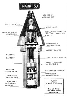
__________________________________________________________________________________
HOT SPOT POINTS
Simply put, hotspots are the physical places where users can wirelessly connect their mobile devices, such as smartphones and tablets, to the Internet. A hotspot can be in a private location or a public one, such as in a coffee shop, a hotel, an airport, or even an airplane.
A WiFi hotspot is simply an area with an accessible wireless network. The term is most often used to refer to wireless networks in public areas like airports and coffee shops. ... You can even create your own mobile hotspot using a cell phone or an external device that can connect to a cellular network.
WiFi is used to access the internet using a device called router. Mobile hotspot is used to share your internet with other phones. ... When you turn your phone or device into a mobile hotspot, you are using your cellular data, and then serving that data to other devices (such as another phone or laptop) using Wi-Fi.
In fact, there is no need to enable a hotspot service using your cell phone carrier. A feature known as Wi-Fi tethering will automatically transform your smartphone into a wireless internet router. ... Even without a data connection, you can still turn your old smartphone into a Wi-Fi hotspot
It's usually more expensive to get the same amount of data from a cellular provider than from home broadband. Finally, a mobile hotspot is less reliable than your home network. So generally speaking, a mobile hotspot can replace your home internet but only when absolutely necessary.
Hotspot (Wi-Fi)
A hotspot is a physical location where people may obtain Internet access, typically using Wi-Fi technology, via a wireless local area network (WLAN) using a router connected to an internet service provider.Public hotspots may be created by a business for use by customers, such as coffee shops or hotels. Public hotspots are typically created from wireless access points configured to provide Internet access, controlled to some degree by the venue. In its simplest form, venues that have broadband Internet access can create public wireless access by configuring an access point (AP), in conjunction with a router and connecting the AP to the Internet connection. A single wireless router combining these functions may suffice.
Private hotspots may be configured on a smartphone or tablet with a mobile network data plan to allow Internet access to other devices via Bluetooth pairing or if both the hotspot device and the device/s accessing it are connected to the same Wi-Fi network.

A diagram showing a Wi-Fi network
The public can use a laptop or other suitable portable device to access the wireless connection (usually Wi-Fi) provided. Of the estimated 150 million laptops, 14 million PDAs, and other emerging Wi-Fi devices sold per year for the last few years, most include the Wi-Fi feature.
The iPass 2014 interactive map, that shows data provided by the analysts Maravedis Rethink, shows that in December 2014 there are 46,000,000 hotspots worldwide and more than 22,000,000 roamable hotspots. More than 10,900 hotspots are on trains, planes and airports (Wi-Fi in motion) and more than 8,500,000 are "branded" hotspots (retail, cafés, hotels). The region with the largest number of public hotspots is Europe, followed by North America and Asia.
Libraries throughout the United States are implementing hotspot lending programs to extend access to online library services to users at home who cannot afford in-home Internet access or do not have access to Internet infrastructure. The New York Public Library was the largest program, lending out 10,000 devices to library patrons. Similar programs have existed in Kansas, Maine, and Oklahoma; and many individual libraries are implementing these programs.
Wi-Fi positioning is a method for geolocation based on the positions of nearby hotspots.
Locations
Public hotspots are often found at airports, bookstores, coffee shops, department stores, fuel stations, hotels, hospitals, libraries, public pay phones, restaurants, RV parks and campgrounds, supermarkets, train stations, and other public places. Additionally, many schools and universities have wireless networks on their campuses.Free hotspots operate in two ways:
- Using an open public network is the easiest way to create a free hotspot. All that is needed is a Wi-Fi router. Similarly, when users of private wireless routers turn off their authentication requirements, opening their connection, intentionally or not, they permit piggybacking (sharing) by anyone in range
- Closed public networks use a HotSpot Management System to control access to hotspots. This software runs on the router itself or an external computer allowing operators to authorize only specific users to access the Internet . Providers of such hotspots often associate the free access with a menu, membership, or purchase limit. Operators may also limit each user's available bandwidth (upload and download speed) to ensure that everyone gets a good quality service. Often this is done through service-level agreements.
Commercial hotspots
A commercial hotspot may feature:- A captive portal / login screen / splash page that users are redirected to for authentication and/or payment. The captive portal / splash page sometimes includes the social login buttons.
- A payment option using a credit card, iPass, PayPal, or another payment service (voucher-based Wi-Fi)
- A walled garden feature that allows free access to certain sites
- Service-oriented provisioning to allow for improved revenue
- Data analytics and data capture tools, to analyze and export data from Wi-Fi clients
Major airports and business hotels are more likely to charge for service, though most hotels provide free service to guests; and increasingly, small airports and airline lounges offer free service. Retail shops, public venues and offices usually provide a free Wi-Fi SSID for their guests and visitors.
Roaming services are expanding among major hotspot service providers. With roaming service the users of a commercial provider can have access to other providers' hotspots, either free of charge or for extra fees, which users will usually be charged on an access-per-minute basis
Software hotspots
Many Wi-Fi adapters built into or easily added to consumer computers and mobile devices include the functionality to operate as private or mobile hotspots, sometimes referred to as "mi-fi". The use of a private hotspot to enable other personal devices to access the WAN (usually but not always the Internet) is a form of bridging, and known as tethering. Manufacturers and firmware creators can enable this functionality in Wi-Fi devices on many Wi-Fi devices, depending upon the capabilities of the hardware, and most modern consumer operating systems, including Android, Apple OS X 10.6 and later,Windows mobile, and Linux include features to support this. Additionally wireless chipset manufacturers such as Atheros, Broadcom, Intel and others, may add the capability for certain Wi-Fi NICs, usually used in a client role, to also be used for hotspot purposes. However, some service providers, such as AT&T, Sprint, and T-Mobile charge users for this service or prohibit and disconnect user connections if tethering is detected.Third-party software vendors offer applications to allow users to operate their own hotspot, whether to access the Internet when on the go, share an existing connection, or extend the range of another hotspot.
_________________________________________________________________________________
SATELLITE POINT IN SPACE
Satellite Internet access
Satellite Internet access is Internet access provided through communications satellites. Modern consumer grade satellite Internet service is typically provided to individual users through geostationary satellites that can offer relatively high data speeds, with newer satellites using Ku band to achieve downstream data speeds up to 506 Mbit/s
WildBlue satellite Internet dish on the side of a house
Function
Satellite Internet generally relies on three primary components: a satellite, typically in geostationary orbit (sometimes referred to as a geosynchronous Earth orbit, or GEO), a number of ground stations known as gateways that relay Internet data to and from the satellite via radio waves (microwave), and a small antenna at the subscriber's location, often a VSAT (very-small-aperture terminal) dish antenna with a transceiver. Other components of a satellite Internet system include a modem at the user end which links the user's network with the transceiver, and a centralized network operations center (NOC) for monitoring the entire system. Working in concert with a broadband gateway, the satellite operates a Star network topology where all network communication passes through the network's hub processor, which is at the center of the star. With this configuration, the number of remote VSATs that can be connected to the hub is virtually limitless.Satellite
Marketed as the center of the new broadband satellite networks are a new generation of high-powered GEO satellites positioned 35,786 kilometres (22,236 mi) above the equator, operating in Ka-band (18.3–30 GHz) mode. These new purpose-built satellites are designed and optimized for broadband applications, employing many narrow spot beams, which target a much smaller area than the broad beams used by earlier communication satellites. This spot beam technology allows satellites to reuse assigned bandwidth multiple times which can enable them to achieve much higher overall capacity than conventional broad beam satellites. The spot beams can also increase performance and consequential capacity by focusing more power and increased receiver sensitivity into defined concentrated areas. Spot beams are designated as one of two types: subscriber spot beams, which transmit to and from the subscriber-side terminal, and gateway spot beams, which transmit to/from a service provider ground station. Note that moving off the tight footprint of a spotbeam can degrade performance significantly. Also, spotbeams can make impossible the use of other significant new technologies including 'Carrier in Carrier' modulation.In conjunction with the satellite's spot-beam technology, a bent-pipe architecture has traditionally been employed in the network in which the satellite functions as a bridge in space, connecting two communication points on the ground. The term "bent-pipe" is used to describe the shape of the data path between sending and receiving antennas, with the satellite positioned at the point of the bend. Simply put, the satellite's role in this network arrangement is to relay signals from the end user's terminal to the ISP's gateways, and back again without processing the signal at the satellite. The satellite receives, amplifies, and redirects a carrier on a specific radio frequency through a signal path called a transponder.
Some proposed satellite constellations in LEO such as SpaceX's Starlink, Telesat's constellation and LeoSat will employ laser communication equipment for high-throughput optical inter-satellite links. The interconnected satellites allow for direct routing of user data from satellite to satellite and effectively create a space-based optical mesh network that will enable seamless network management and continuity of service.
The satellite has its own set of antennas to receive communication signals from Earth and to transmit signals to their target location. These antennas and transponders are part of the satellite's "payload", which is designed to receive and transmit signals to and from various places on Earth. What enables this transmission and reception in the payload transponders is a repeater subsystem (RF (radio frequency) equipment) used to change frequencies, filter, separate, amplify and group signals before routing them to their destination address on Earth. The satellite's high-gain receiving antenna passes the transmitted data to the transponder which filters, translates and amplifies them, then redirects them to the transmitting antenna on board. The signal is then routed to a specific ground location through a channel known as a carrier. Beside the payload, the other main component of a communications satellite is called the bus, which comprises all equipment required to move the satellite into position, supply power, regulate equipment temperatures, provide health and tracking information, and perform numerous other operational tasks.
Gateways
Along with dramatic advances in satellite technology over the past decade, ground equipment has similarly evolved, benefiting from higher levels of integration and increasing processing power, expanding both capacity and performance boundaries. The Gateway—or Gateway Earth Station (its full name)—is also referred to as a ground station, teleport or hub. The term is sometimes used to describe just the antenna dish portion, or it can refer to the complete system with all associated components. In short, the gateway receives radio wave signals from the satellite on the last leg of the return or upstream payload, carrying the request originating from the end-user's site. The satellite modem at the gateway location demodulates the incoming signal from the outdoor antenna into IP packets and sends the packets to the local network. Access server/gateways manage traffic transported to/from the Internet. Once the initial request has been processed by the gateway's servers, sent to and returned from the Internet, the requested information is sent back as a forward or downstream payload to the end-user via the satellite, which directs the signal to the subscriber terminal. Each Gateway provides the connection to the Internet backbone for the gateway beam(s) it serves. The system of gateways comprising the satellite ground system provides all network services for satellite and corresponding terrestrial connectivity. Each gateway provides a multiservice access network for subscriber terminal connections to the Internet. In the continental United States, because it is north of the equator, all gateway and subscriber dish antenna must have an unobstructed view of the southern sky. Because of the satellite's geostationary orbit, the gateway antenna can stay pointed at a fixed position.Antenna dish and modem
For the customer-provided equipment (i.e. PC and router) to access the broadband satellite network, the customer must have additional physical components installed:Outdoor unit (ODU)
At the far end of the outdoor unit is typically a small (2–3-foot diameter), reflective dish-type radio antenna. The VSAT antenna must also have an unobstructed view of the sky to allow for proper line-of-sight (L-O-S) to the satellite. There are three physical characteristic settings used to ensure that the antenna is configured correctly at the satellite, which are: azimuth, elevation, polarization, and skew. The combination of these settings gives the outdoor unit a L-O-S to the chosen satellite and makes data transmission possible. These parameters are generally set at the time the equipment is installed, along with a beam assignment (Ka-band only); these steps must all be taken prior to the actual activation of service. Transmit and receive components are typically mounted at the focal point of the antenna which receives/sends data from/to the satellite. The main parts are:- Feed – This assembly is part of the VSAT receive and transmit chain, which consists of several components with different functions, including the feed horn at the front of the unit, which resembles a funnel and has the task of focusing the satellite microwave signals across the surface of the dish reflector. The feed horn both receives signals reflected off the dish's surface and transmits outbound signals back to the satellite.
- Block upconverter (BUC) – This unit sits behind the feed horn and may be part of the same unit, but a larger (higher wattage) BUC could be a separate piece attached to the base of the antenna. Its job is to convert the signal from the modem to a higher frequency and amplify it before it is reflected off the dish and towards the satellite.
- Low-noise block downconverter (LNB) – This is the receiving element of the terminal. The LNB's job is to amplify the received satellite radio signal bouncing off the dish and filter out the noise, which is any signal not carrying valid information. The LNB passes the amplified, filtered signal to the satellite modem at the user's location.
Indoor unit (IDU)
The satellite modem serves as an interface between the outdoor unit and customer-provided equipment (i.e. PC, router) and controls satellite transmission and reception. From the sending device (computer, router, etc.) it receives an input bitstream and converts or modulates it into radio waves, reversing that order for incoming transmissions, which is called demodulation. It provides two types of connectivity:- Coaxial cable (COAX) connectivity to the satellite antenna. The cable carrying electromagnetic satellite signals between the modem and the antenna generally is limited to be no more than 150 feet in length.
- Ethernet connectivity to the computer, carrying the customer's data packets to and from the Internet content servers.
Challenges and limitations
Signal latency
Latency (commonly referred to as "ping time") is the delay between requesting data and the receipt of a response, or in the case of one-way communication, between the actual moment of a signal's broadcast and the time it is received at its destination.A radio signal takes about 120 milliseconds to reach a geostationary satellite and then 120 milliseconds to reach the ground station, so nearly 1/4 of a second overall. Typically, during perfect conditions, the physics involved in satellite communications account for approximately 550 milliseconds of latency round-trip time.
The longer latency is the primary difference between a standard terrestrial-based network and a geostationary satellite-based network. The round-trip latency of a geostationary satellite communications network can be more than 12 times that of a terrestrial based network.
Geostationary orbits
A geostationary orbit (or geostationary Earth orbit/GEO) is a geosynchronous orbit directly above the Earth's equator (0° latitude), with a period equal to the Earth's rotational period and an orbital eccentricity of approximately zero (i.e. a "circular orbit"). An object in a geostationary orbit appears motionless, at a fixed position in the sky, to ground observers. Launchers often place communications satellites and weather satellites in geostationary orbits, so that the satellite antennas that communicate with them do not have to move to track them, but can point permanently at the position in the sky where the satellites stay. Due to the constant 0° latitude and circularity of geostationary orbits, satellites in GEO differ in location by longitude only.Compared to ground-based communication, all geostationary satellite communications experience higher latency due to the signal having to travel 35,786 km (22,236 mi) to a satellite in geostationary orbit and back to Earth again. Even at the speed of light (about 300,000 km/s or 186,000 miles per second), this delay can appear significant. If all other signaling delays could be eliminated, it still takes a radio signal about 250 milliseconds (ms), or about a quarter of a second, to travel to the satellite and back to the ground. The absolute minimum total amount of delay varies, due to the satellite staying in one place in the sky, while ground-based users can be directly below (with a roundtrip latency of 239.6 ms), or far to the side of the planet near the horizon (with a roundtrip latency of 279.0 ms).
For an Internet packet, that delay is doubled before a reply is received. That is the theoretical minimum. Factoring in other normal delays from network sources gives a typical one-way connection latency of 500–700 ms from the user to the ISP, or about 1,000–1,400 ms latency for the total round-trip time (RTT) back to the user. This is more than most dial-up users experience at typically 150–200 ms total latency, and much higher than the typical 15–40 ms latency experienced by users of other high-speed Internet services, such as cable or VDSL.
For geostationary satellites, there is no way to eliminate latency, but the problem can be somewhat mitigated in Internet communications with TCP acceleration features that shorten the apparent round trip time (RTT) per packet by splitting ("spoofing") the feedback loop between the sender and the receiver. Certain acceleration features are often present in recent technology developments embedded in satellite Internet equipment.
Latency also impacts the initiation of secure Internet connections such as SSL which require the exchange of numerous pieces of data between web server and web client. Although these pieces of data are small, the multiple round-trips involved in the handshake produce long delays compared to other forms of Internet connectivity, as documented by Stephen T. Cobb in a 2011 report published by the Rural Mobile and Broadband Alliance.This annoyance extends to entering and editing data using some Software as a Service or SaaS applications as well as in other forms of online work.
One should thoroughly test the functionality of live interactive access to a distant computer—such as virtual private networks. Many TCP protocols were not designed to work in high-latency environments.
Medium and Low Earth Orbits
Medium Earth orbit (MEO) and low Earth orbit (LEO) satellite constellations do not have such great delays, as the satellites are closer to the ground. For example:- The current LEO constellations of Globalstar and Iridium satellites have delays of less than 40 ms round trip, but their throughput is less than broadband at 64 kbit/s per channel. The Globalstar constellation orbits 1,420 km above the Earth and Iridium orbits at 670 km altitude.
- The O3b Networks MEO constellation orbits at 8,062 km, with RTT latency of approximately 125 ms. The proposed new network is also designed for much higher throughput with links well in excess of 1 Gbit/s (Gigabits per second).
One can communicate with MEO or LEO satellites that move in the sky in three ways, using:
- more diffuse or completely omnidirectional ground antennas capable of communicating with one or more satellites visible in the sky at the same time, but at significantly higher transmit power than fixed geostationary dish antennas (due to the lower gain), and with much poorer signal-to-noise ratios for receiving the signal
- motorized antenna mounts with high-gain, narrow beam antennas tracking individual satellites
- phased array antennas that can steer the beam electronically, together with software that can predict the path of each satellite in the constellation
Ultralight atmospheric aircraft as satellites
A proposed alternative to relay satellites is a special-purpose solar-powered ultralight aircraft, which would fly along a circular path above a fixed ground location, operating under autonomous computer control at a height of approximately 20,000 meters.For example, the United States Defense Advanced Research Projects Agency Vulture project envisaged an ultralight aircraft capable of station-keeping over a fixed area for a period of up to five years, and able to provide both continuous surveillance to ground assets as well as to service extremely low-latency communications networks. This project was cancelled[by whom?] in 2012 before it became operational.[citation needed]
Onboard batteries would charge during daylight hours through solar panels covering the wings, and would provide power to the plane during night. Ground-based satellite internet dishes would relay signals to and from the aircraft, resulting in a greatly reduced round-trip signal latency of only 0.25 milliseconds. The planes could potentially run for long periods without refueling. Several such schemes involving various types of aircraft have been proposed in the past.
Interference

A foldable Bigpond satellite Internet dish
Rain margins are the extra communication link requirements needed to account for signal degradations due to moisture and precipitation, and are of acute importance on all systems operating at frequencies over 10 GHz.
The amount of time during which service is lost can be reduced by increasing the size of the satellite communication dish so as to gather more of the satellite signal on the downlink and also to provide a stronger signal on the uplink. In other words, increasing antenna gain through the use of a larger parabolic reflector is one way of increasing the overall channel gain and, consequently, the signal-to-noise (S/N) ratio, which allows for greater signal loss due to rain fade without the S/N ratio dropping below its minimum threshold for successful communication.
Modern consumer-grade dish antennas tend to be fairly small, which reduces the rain margin or increases the required satellite downlink power and cost. However, it is often more economical to build a more expensive satellite and smaller, less expensive consumer antennas than to increase the consumer antenna size to reduce the satellite cost.
Large commercial dishes of 3.7 m to 13 m diameter can be used to achieve increased rain margins and also to reduce the cost per bit by allowing for more efficient modulation codes. Alternately, larger aperture antennae can require less power from the satellite to achieve acceptable performance. Satellites typically use photovoltaic solar power, so there is no expense for the energy itself, but a more powerful satellite will require larger, more powerful solar panels and electronics, often including a larger transmitting antenna. The larger satellite components not only increase materials costs but also increase the weight of the satellite, and in general, the cost to launch a satellite into an orbit is directly proportional to its weight. (In addition, since satellite launch vehicles [i.e. rockets] have specific payload size limits, making parts of the satellite larger may require either more complex folding mechanisms for parts of the satellite like solar panels and high-gain antennas, or upgrading to a more expensive launch vehicle that can handle a larger payload.)
Modulated carriers can be dynamically altered in response to rain problems or other link impairments using a process called adaptive coding and modulation, or "ACM". ACM allows the bit rates to be increased substantially during normal clear sky conditions, increasing the number of bits per Hz transmitted, and thus reducing overall cost per bit. Adaptive coding requires some sort of a return or feedback channel which can be via any available means, satellite or terrestrial.
Line of sight

Fresnel zone. D is the distance between the transmitter and the receiver, r is the radius of the Fresnel zone.
Typically a completely clear line of sight between the dish and the satellite is required for the system to work optimally. In addition to the signal being susceptible to absorption and scattering by moisture, the signal is similarly impacted by the presence of trees and other vegetation in the path of the signal. As the radio frequency decreases, to below 900 MHz, penetration through vegetation increases, but most satellite communications operate above 2 GHz making them sensitive to even minor obstructions such as tree foliage. A dish installation in the winter must factor in plant foliage growth that will appear in the spring and summer.
Fresnel zone
Even if there is a direct line of sight between the transmitting and receiving antenna, reflections from objects near the path of the signal can decrease apparent signal power through phase cancellations. Whether and how much signal is lost from a reflection is determined by the location of the object in the Fresnel zone of the antennas.Two-way satellite-only communication

The back panel of a satellite modem, with coaxial connections for both incoming and outgoing signals, and an Ethernet port for connection
There are several types of two way satellite Internet services, including time division multiple access (TDMA) and single channel per carrier (SCPC). Two-way systems can be simple VSAT terminals with a 60–100 cm dish and output power of only a few watts intended for consumers and small business or larger systems which provide more bandwidth. Such systems are frequently marketed as "satellite broadband" and can cost two to three times as much per month as land-based systems such as ADSL. The modems required for this service are often proprietary, but some are compatible with several different providers. They are also expensive, costing in the range of USD $600 to $2000.

The two-way "iLNB" used on the SES Broadband.
Bandwidth
Consumer satellite Internet customers range from individual home users with one PC to large remote business sites with several hundred PCs.Home users tend to use shared satellite capacity to reduce the cost, while still allowing high peak bit rates when congestion is absent. There are usually restrictive time-based bandwidth allowances so that each user gets their fair share, according to their payment. When a user exceeds their allowance, the company may slow down their access, deprioritise their traffic or charge for the excess bandwidth used. For consumer satellite Internet, the allowance can typically range from 200 MB per day to 25 GB per month. A shared download carrier may have a bit rate of 1 to 40 Mbit/s and be shared by up to 100 to 4,000 end users.
The uplink direction for shared user customers is normally time division multiple access (TDMA), which involves transmitting occasional short packet bursts in between other users (similar to how a cellular phone shares a cell tower).
Each remote location may also be equipped with a telephone modem; the connections for this are as with a conventional dial-up ISP. Two-way satellite systems may sometimes use the modem channel in both directions for data where latency is more important than bandwidth, reserving the satellite channel for download data where bandwidth is more important than latency, such as for file transfers.
In 2006, the European Commission sponsored the UNIC project which aims at developing an end-to-end scientific test bed for the distribution of new broadband interactive TV-centric services delivered over low-cost two-way satellite to actual end-users in the home. The UNIC architecture employs DVB-S2 standard for downlink and DVB-RCS standard for uplink.
Normal VSAT dishes (1.2–2.4 m diameter) are widely used for VoIP phone services. A voice call is sent by means of packets via the satellite and Internet. Using coding and compression techniques the bit rate needed per call is only 10.8 kbit/s each way.
Portable satellite Internet
Portable satellite modem

Portable Satellite Internet Modem and Antenna deployed with the Red Cross in South Sudan.
Using such a modem is extremely expensive—data transfer costs between $5 and $7 per megabyte. The modems themselves are also expensive, usually costing between $1,000 and $5,000.
Internet via satellite phone
For many years satellite phones have been able to connect to the Internet. Bandwidth varies from about 2400 bit/s for Iridium network satellites and ACeS based phones to 15 kbit/s upstream and 60 kbit/s downstream for Thuraya handsets. Globalstar also provides Internet access at 9600 bit/s—like Iridium and ACeS a dial-up connection is required and is billed per minute, however both Globalstar and Iridium are planning to launch new satellites offering always-on data services at higher rates. With Thuraya phones the 9,600 bit/s dial-up connection is also possible, the 60 kbit/s service is always-on and the user is billed for data transferred (about $5 per megabyte). The phones can be connected to a laptop or other computer using a USB or RS-232 interface. Due to the low bandwidths involved it is extremely slow to browse the web with such a connection, but useful for sending email, Secure Shell data and using other low-bandwidth protocols. Since satellite phones tend to have omnidirectional antennas no alignment is required as long as there is a line of sight between the phone and the satellite.One-way receive, with terrestrial transmit
One-way terrestrial return satellite Internet systems are used with conventional dial-up Internet access, with outbound (upstream) data traveling through a telephone modem, but downstream data sent via satellite at a higher rate. In the U.S., an FCC license is required for the uplink station only; no license is required for the users.Another type of 1-way satellite Internet system uses General Packet Radio Service (GPRS) for the back-channel. Using standard GPRS or Enhanced Data Rates for GSM Evolution (EDGE), costs are reduced for higher effective rates if the upload volume is very low, and also because this service is not per-time charged, but charged by volume uploaded. GPRS as return improves mobility when the service is provided by a satellite that transmits in the field of 100-200 kW.[citation needed] Using a 33 cm wide satellite dish, a notebook and a normal GPRS equipped GSM phone, users can get mobile satellite broadband.
System components
The transmitting station has two components, consisting of a high speed Internet connection to serve many customers at once, and the satellite uplink to broadcast requested data to the customers. The ISP's routers connect to proxy servers which can enforce quality of service (QoS) bandwidth limits and guarantees for each customer's traffic.Often, nonstandard IP stacks are used to address the latency and asymmetry problems of the satellite connection. As with one-way receive systems, data sent over the satellite link is generally also encrypted, as otherwise it would be accessible to anyone with a satellite receiver.
Many IP-over-satellite implementations use paired proxy servers at both endpoints so that certain communications between clients and servers need not to accept the latency inherent in a satellite connection. For similar reasons, there exist special Virtual private network (VPN) implementations designed for use over satellite links because standard VPN software cannot handle the long packet travel times.
Upload speeds are limited by the user's dial-up modem, while download speeds can be very fast compared to dial-up, using the modem only as the control channel for packet acknowledgement.
Latency is still high, although lower than full two-way geostationary satellite Internet, since only half of the data path is via satellite, the other half being via the terrestrial channel.
One-way broadcast, receive only
One-way broadcast satellite Internet systems are used for Internet Protocol (IP) broadcast-based data, audio and video distribution. In the U.S., a Federal Communications Commission (FCC) license is required only for the uplink station and no license is required for users. Note that most Internet protocols will not work correctly over one-way access, since they require a return channel. However, Internet content such as web pages can still be distributed over a one-way system by "pushing" them out to local storage at end user sites, though full interactivity is not possible. This is much like TV or radio content which offers little user interface.The broadcast mechanism may include compression and error correction to help ensure the one-way broadcast is properly received. The data may also be rebroadcast periodically, so that receivers that did not previously succeed will have additional chances to try downloading again.
The data may also be encrypted, so that while anyone can receive the data, only certain destinations are able to actually decode and use the broadcast data. Authorized users only need to have possession of either a short decryption key or an automatic rolling code device that uses its own highly accurate independent timing mechanism to decrypt the data.
System hardware components
Similar to one-way terrestrial return, satellite Internet access may include interfaces to the public switched telephone network for squawk box applications. An Internet connection is not required, but many applications include a File Transfer Protocol (FTP) server to queue data for broadcast.System software components
Most one-way broadcast applications require custom programming at the remote sites. The software at the remote site must filter, store, present a selection interface to and display the data. The software at the transmitting station must provide access control, priority queuing, sending, and encapsulating of the data.Services
Emerging commercial services in this area include:- Outernet – Satellite constellation technology
Efficiency increases
2013 FCC report cites big jump in satellite performance
In its report released in February, 2013, the Federal Communications Commission noted significant advances in satellite Internet performance. The FCC's Measuring Broadband America report also ranked the major ISPs by how close they came to delivering on advertised speeds. In this category, satellite Internet topped the list, with 90% of subscribers seeing speeds at 140% or better than what was advertised.Reducing satellite latency
Much of the slowdown associated with satellite Internet is that for each request, many roundtrips must be completed before any useful data can be received by the requester. Special IP stacks and proxies can also reduce latency through lessening the number of roundtrips, or simplifying and reducing the length of protocol headers. Optimization technologies include TCP acceleration, HTTP pre-fetching and DNS caching among many others. See the Space Communications Protocol Specifications standard (SCPS), developed by NASA and adopted widely by commercial and military equipment and software providers in the market space.Satellites launched
The WINDS satellite was launched on February 23, 2008. The WINDS satellite is used to provide broadband Internet services to Japan and locations across the Asia-Pacific region. The satellite to provides a maximum speed of 155 Mbit/s down and 6 Mbit/s up to residences with a 45 cm aperture antenna and a 1.2 Gbit/s connection to businesses with a 5-meter antenna. It has reached the end of its design life expectancy.SkyTerra-1 was launched in mid-November 2010, providing North America, while Hylas-1 was launched in November 2010, targeting Europe.
On December 26, 2010, Eutelsat's KA-SAT was launched. It covers the European continent with 80 spot beams—focused signals that cover an area a few hundred kilometers across Europe and the Mediterranean. Spot beams allow for frequencies to be effectively reused in multiple regions without interference. The result is increased capacity. Each of the spot beams has an overall capacity of 900 Mbit/s and the entire satellite will has a capacity of 70 Gbit/s.
ViaSat-1, the highest capacity communications satellite in the world, was launched Oct. 19, 2011 from Baikonur, Kazakhstan, offering 140 Gbit/s of total throughput capacity, through the Exede Internet service.
Passengers aboard JetBlue Airways can use this service since 2015.The service has also been expanded to United Airlines, American Airlines, Scandinavian Airlines, Virgin America and Qantas.
The EchoStar XVII satellite was launched July 5, 2012 by Arianespace and was placed in its permanent geosynchronous orbital slot of 107.1° West longitude, servicing HughesNet. This Ka-band satellite has over 100 Gbit/s of throughput capacity.
Since 2013, the O3b satellite constellation claims an end-to-end round-trip latency of 238 ms for data services.
In 2015 and 2016, the Australian Government launched two satellites to provide internet to regional Australians and residents of External Territories, such as Norfolk Island and Christmas Island.
__________________________________________________________________________________
ELASTICITY ELECTRON IN SPACE
The Electron Spin as Resulting From the Ether Elasticity
We recall how the Maxwell equations ensue from the Navier-Stokes-Durand equation of elasticity that governs the field of the displacements of the points of the ether shown to be an elastic medium. Such a field can be constituted by waves propagated in this ether. In previous papers we have generalized the waves associated to photons to waves associated to , (i.e., particles of mass m and electrical charges e), and demonstrated that a moving , as, e.g., an electron is a superposition of waves that forms a small globule moving with the velocity V of this . That is to say that a moving particle is a moving small globule of ether deformation. Now in its motion, creates out side of it, a field of ether deformation from witch ensues the electromagnetic field created by . The induced field being denoted without ambiguity also simply by , it appears, as shown here below, that the magnetic field H ensuing from , is the field of the local velocities of the points of the ether, i.e., . The fundamental fact that we demonstrate, is that on a fixed observatory point near at a given instant to the moving electron, i.e., to the moving , the velocity of the ether denoted there by is of the same form as the velocity of a point of a rotating solid. This phenomenon is the spin of the electron, that, in a quantum state of an atom can take only quantized values.
Electron scattering

Electron scattering occurs when electrons are deviated from their original trajectory. This is due to the electrostatic forces within matter interaction or, if an external magnetic field is present, the electron may be deflected by the Lorentz force.This scattering typically happens with solids such as metals, semiconductors and insulator ] and is a limiting factor in integrated circuits and transistors.
The application of electron scattering is such that it can be used as a high resolution microscope for hadronic systems, that allows the measurement of the distribution of charges for nucleons and nuclear structure.The scattering of electrons has allowed us to understand that protons and neutrons are made up of the smaller elementary subatomic particles called quarks
Electrons may be scattered through a solid in several ways:
- Not at all: no electron scattering occurs at all and the beam passes straight through.
- Single scattering: when an electron is scattered just once.
- Plural scattering: when electron(s) scatter several times.
- Multiple scattering: when electron(s) scatter very many times over.
Phenomena
Electrons can be scattered by other charged particles through the electrostatic Coulomb forces. Furthermore, if a magnetic field is present, a traveling electron will be deflected by the Lorentz force. An extremely accurate description of all electron scattering, including quantum and relativistic aspects, is given by the theory of quantum electrodynamics.Lorentz force

Path of an electron of velocity v moving in a magnetic field B. Where the dotted circle indicates the magnetic field directed out of the plane, and the crossed circle indicates the magnetic field directed into the plane.

And qv x B describes the magnetic force due to a present magnetic field, B, acting on q when q is moving with velocity v.
Which can also be written as:
![{\mathbf {F}}=q[-\nabla \phi -{\frac {d{\mathbf {A}}}{dt}}+\nabla ({\mathbf {A}}\cdot {\mathbf {v}})]](https://wikimedia.org/api/rest_v1/media/math/render/svg/e7a85073a0f8338eb41180c17d00046603f4d7b3)

It was Oliver Heaviside who is attributed in 1885 and 1889 to first deriving the correct expression for the Lorentz force of qv x B.[16] Hendrik Lorentz derived and refined the concept in 1892 and gave it his name, incorporating forces due to electric fields.
Rewriting this as the equation of motion for a free particle of charge q mass m,this becomes:


Variations on this basic formula describe the magnetic force on a current-carrying wire (sometimes called Laplace force), the electromotive force in a wire loop moving through a magnetic field (an aspect of Faraday's law of induction), and the force on a particle which might be traveling near the speed of light (relativistic form of the Lorentz force).
Electrostatic Coulomb force

The absolute value of the force F between two point charges q and Q relates to the distance r
between the point charges and to the simple product of their charges.
The diagram shows that like charges repel each other, and opposite
charges attract each other.

In the image, the vector F1 is the force experienced by q1, and the vector F2 is the force experienced by q2. When q1q2 > 0 the forces are repulsive (as in the image) and when q1q2 < 0 the forces are attractive (opposite to the image). The magnitude of the forces will always be equal. In this case:
where the vector,
is the vectorial distance between the charges and,
(a unit vector pointing from q2 to q1).
The vector form of the equation above calculates the force F1 applied on q1 by q2. If r12 is used instead, then the effect on q2 can be found. It can be also calculated using Newton's third law: F2 = -F1.

where the vector,

is the vectorial distance between the charges and,

(a unit vector pointing from q2 to q1).
The vector form of the equation above calculates the force F1 applied on q1 by q2. If r12 is used instead, then the effect on q2 can be found. It can be also calculated using Newton's third law: F2 = -F1.
Coulomb's law states that:
- The magnitude of the electric force between two point charges is directly proportional to the product of the charges and inversely proportional to the square of the distance between them.


Collisions
If two particles interact with one another in a collision process there are four results possible after the interaction:Elastic
Elastic scattering is when the collisions between target and incident particles have total conservation of kinetic energy] This implies that there is no breaking up of the particles or energy loss through vibrations,] that is to say that the internal states of each of the particles remains unchanged. Due to the fact that there is no breaking present, elastic collisions can be modeled as occurring between point-like particles, a principle that is very useful for an elementary particle such as the electron.Inelastic
Inelastic scattering is when the collisions do not conserve kinetic energy, and as such the internal states of one or both of the particles has changed. This is due to energy being converted into vibrations which can be interpreted as heat, waves (sound), or vibrations between constituent particles of either collision party. Particles may also split apart, further energy can be converted into breaking the chemical bonds between components.Furthermore, momentum is conserved in both elastic and inelastic scattering.] The other two results are reactions (when the structure of the interacting particles is changed producing two or more (generally complex particles)), and that new particles that are not constituent elementary particles of the interacting particles are created.
Types of scattering
Compton scattering

Compton Scattering Feynman Diagram
Compton scattering, so named for Arthur Compton who first observed the effect in 1922 and which earned him the 1927 Nobel Prize in Physics; is the inelastic scattering of a high-energy photon by a free charged particle. [note 6]
This was demonstrated in 1923 by firing radiation of a given wavelength (X-rays in the given case) through a foil (carbon target), which was scattered in a manner inconsistent with classical radiation theory.[26][note 7] Compton published a paper in the Physical Review explaining the phenomenon: A quantum theory of the scattering of X-rays by light elements. The Compton effect can be understood as high-energy photons scattering in-elastically off individual electrons,when the incoming photon gives part of its energy to the electron, then the scattered photon has lower energy and lower frequency and longer wavelength according to the Planck relation:

This was an important discovery during the 1920s when the particle (photon) nature of light suggested by the Photoelectric effect was still being debated, the Compton experiment gave clear and independent evidence of particle-like behavior.
The formula describing the Compton shift in the wavelength due to scattering is given by:

The coefficient of (1 - cosθ) is known as the Compton wavelength, but is in fact a proportionality constant for the wavelength shift. The collision causes the photon wavelength to increase by somewhere between 0 (for a scattering angle of 0°) and twice the Compton wavelength (for a scattering angle of 180°).
Thomson scattering is the classical elastic quantitative interpretation of the scattering process, and this can be seen to happen with lower, mid-energy, photons. The classical theory of an electromagnetic wave scattered by charged particles, cannot explain low intensity shifts in wavelength.
Inverse Compton scattering takes place when the electron is moving, and has sufficient kinetic energy compared to the photon. In this case net energy may be transferred from the electron to the photon. The inverse Compton effect is seen in astrophysics when a low energy photon (e.g. of the cosmic microwave background) bounces off a high energy (relativistic) electron. Such electrons are produced in supernovae and active galactic nuclei.
Møller scattering

Møller scattering Feynman diagram
Mott scattering
Bhabha scattering
Bremsstrahlung scattering
Deep inelastic scattering
Synchrotron emission
If a charged particle such as an electron is accelerated – this can be acceleration in a straight line or motion in a curved path – electromagnetic radiation is emitted by the particle. Within electron storage rings and circular particle accelerators known as synchrotrons, electrons are bent in a circular path and emit X-rays typically. This radially emitted () electromagnetic radiation when charged particles are accelerated is called synchrotron radiation. It is produced in synchrotrons using bending magnets, undulators and/or wigglers.
The first observation came at the General Electric Research Laboratory in Schenectady, New York, on April 24, 1947, in the synchrotron built by a team of Herb Pollack to test the idea of phase-stability principle for RF accelerators.[note 8] When the technician was asked to look around the shielding with a large mirror to check for sparking in the tube, he saw a bright arc of light coming from the electron beam. Robert Langmuir is credited as recognizing it as synchrotron radiation or, as he called it, "Schwinger radiation" after Julian Schwinger.
Classically, the radiated power P from an accelerated electron is:

- ,


Facilities
SLAC

Aerial photo of the Stanford Linear Accelerator Center, with detector complex at the right (east) side
The SLAC aims to be a premier accelerator laboratory, to pursue strategic programs in particle physics, particle astrophysics and cosmology, as well as the applications in discovering new drugs for healing, new materials for electronics and new ways to produce clean energy and clean up the environment.] Under the directorship of Chi-Chang Kao the SLAC's fifth director (as of November 2012), a noted X-ray scientist who came to SLAC in 2010 to serve as associate laboratory director for the Stanford Synchrotron Radiation Lightsource
______________________________________________________________________
Flexibility Optimized Control for Robot Efficient Moving
The speed of mobile robots moving in corridors is important for the efficiency of material transportation. This paper proposes a novel control method based on the viability theory for optimizing the flexibility of robots passing through narrow corridors. The viability theory can take both environmental constraints and robot dynamical limitation into account simultaneously. The viability of a straight corridor is first analyzed. Then, this analysis is extended to the corner. With these two typical environments, a general corridor working scenario for a mobile robot can be formulated. Through the viability analyses, the largest safety area of the corridor is provided with respect to the robot traveling at a high speed. Furthermore, with the facility of viability, a flexibility optimized control is derived by modifying a general model predictive control framework. The simulation results validate that the proposed flexible control method is secure, accurate, efficient, and lower computational burden. With these properties, this method can also be applied in the area of autonomous vehicle control.

Flexibility analysis of a vertical corner in xy coordinate.
High transportation speed is important for logistics robots applied in industry. In the industry scenario, such as the factory, warehouse, hospital, etc., the moving space of robots is limited because they are generally working in the form of corridors with lots of corners. The traditional robot control methods require deceleration for safety, when the robot encountering the corner or obstacles (one can regard the corner as a static obstacle, where the robot should turn for avoiding). This would reduce the efficiency of material transportation. The main reason for corner deceleration is that the traditional methods do not perfectly combine complexity of the environment with the dynamic of the robot, which would affect the efficiency of obstacle avoidance.
Since the robot model is not needed, these methods are applied widely. But the performances of these methods are conservative, because they cannot guarantee the dynamics of the robot conform to the feature of the environment.Thus, In order to control the robot to avoid obstacles in a higher speed, the dynamic model must be taken into account for the robot trajectory forecasting . The trajectory forecasting method is usually based on stochastic or deterministic models. The stochastic model forecasts the trajectory of the robot with hazard control, which includes the stochastic switched auto regressive model , the hidden Markov model , the neural network , the Bayesian network , the Support Vector Machine , and the Gaussian Mixture Model (GMM) . These models are trained by robot running data, such as velocity, acceleration, orientation angle, etc., and can be used flexibly for robot control.
Nonetheless, if the training data is difficult to cover the necessary states space, especially for the dangerous states of the robot, these methods might cause serious accidents when controlling the robots for obstacle avoidance. Alternatively, the deterministic model is built by equations with physical meanings of the robot , so that it can predict the trajectories of the robot in all circumstances. Obstacle avoidance methods based on deterministic models include Curvature Velocity Method (CVM) , Dynamic Window Approach (DWA) and Lane Curvature Method , etc.
However, for deterministic model, due to the diversity of the control input, the forecasted robot trajectory would have multiple possibilities. Hence considering all aspects of driving behavior during obstacle avoidance would leads to huge computation load, such as DWA* , Control Lyapunov Function (CLF) , path planning , etc. These methods are based on searching or optimizing process, which can predict multiple trajectories by means of the robot models in the local area. Then search the most suitable one for the local environment, which is acquired by the robot sensor. Apparently, a qualified control method should fit the dynamical evolution of the robot into the environment with the ability to select the optimized control in the control space. Model Predictive Control (MPC) can consider the constraints of the environment, limitation of the robot control and the robot dynamics simultaneously, then provides the optimized control signals, which has aroused widespread concern of the researchers today A common MPC structure for mobile robot moving in an obstacles environment can be represented by the following Constrained Finite Time Optimal Control (CFTOC) problem
For optimizing, all the possible controls and robot states should be considered, which are difficult to treat in two aspects. One difficulty is the complexity of the environments, such as non-convex and non-differentiable, such as a corner of the robot working corridor. Hence using a suitable environmental model is essential for the MPC computing, which will reduce the difficulty of the complex environment. Therefore, this issue is extensively investigated by using different representations to interpret the environment. For instance, represented the environment by ellipses to change the non-convex environment to the convex constraints. A chance-constrained approach is applied in to analyze the obstacles of the environment. Liu et al. solved the problem by representing the safe environment as line segments. On the other hand, another difficulty for optimazition is on the all possible robot control inputs which would produce a variety of trajectories for mobile prediction. The control of the robots are generally in a continuous range, which will generate considerable trajectories. It would cost too much computing resources, if choose the optimized trajectory among all possible ones.
Viability was first introduced by Aubin to describe the dynamical adaptation of an evolutionary systems to the environment, which is wildly used for dynamical safety control,
However, the robot working conditions are always non-convex and non-smooth. Our previous work can deal with this complexity of the environment with solid arguments , but did not use the viability kernel to directly control the unmanned vehicle. Based on this previous work, in this paper, we propose a novel model predictive control method based on viability kernel, which can flexibly guide a car-like robot running in the corner of corridors without deceleration.
_________________________________________________________________________________
Gen.MAC.TECH Zone MARIA PREFER n reviewing the meeting points of the elasticity of electrons
__________________________________________________________________________________
I want to to thank you for this very good read. I absolutely enjoyed every little bit of it.Keep doing this, it will be very helpful.
BalasHapusInline soldering robot
Thank you for sharing your info. I really appreciate your efforts and I am waiting for your next post thank you once again.
BalasHapusGeweldige service voor borduren op kleding! Hoogwaardige borduurkwaliteit met een professionele afwerking. Ik beveel Borduurservice België ten zeerste aan voor gepersonaliseerde kleding.
BalasHapus