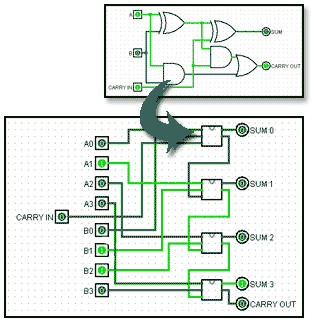
If I need to convert 4 bit input to 8 bits then my input needs to be 8 bits instead of 4 bits, right? So you are recommending I sign extend both inputs to 8 bits and then add them? Doesn't overflow always happen when i am adding binary numbers with the same sign bit? so won't I get overflow regardless of my design?
I was trying to figure out A - B which means A + -B and got the circuit to somewhat work. But something does not seem right. The fourth bit sometimes produce a different result when I add 2's complement binary numbers
The Z80 microprocessor has a bunch of highly versatile and versatile instructions available on some 8-bit microprocessors. It includes unique operations such as block removal for fast and efficient data transfer in memory or between memory and I / O. It also allows multiple bit operations in multiple locations in memory.
The Zilog Z80 microprocessor instructions are divided into the following categories:• 8-bit loading• 16-bit loading• Exchange, block transfer and search• 8-bit logic and arithmetic operations• Multipurpose arithmetic and CPU control• Turnover (rotation) and shift (shift)• Operation set, reset and bit test•Leap• Call, return (return) and restart• Input and output operations
A number of different addressing modes are implemented to allow fast and efficient data transfer between registers, memory locations and input / output devices. Addressing modes included:• Fast (immediate)• Rapid expansion (immediate extended)• Modified page zero• Relative (relative)• Extended (Extended)• Indexed (Indexed)•Register• Indirect register• Implied• Bit
Supporting Chips
Microprocessors come along with a set of peripheral supporters known as Z80 family peripherals. The peripherals that support the Z80 microprocessor include:• Parallel Input / Output Controller (Z80 PIO: Parallel Input / Output)• Input / Serial Output Controller (Z80 SIO: Serial Input / Output)• Timing Circuit / Counter (Z80 CTC: Counter / Timer Circuit)• Direct Memory Access Controller (Z80 DMA: Direct Memory Access)• Double Unsync Receiver / Receiver (Z80 DART: Dual Asynchronous Receiver / Transmitter)
The Z80 microprocessor can not only interface with Z80 family peripherals only, but can be linked to peripherals from other microprocessor families such as Intel's peripheral output. Because these two microprocessors are still one clump (offspring).
Previously we will peel the electronic circuit in zi log 80 described below :
Power, Speed and Compatibility
The logic gates are available in different combinations within I/C packages. As well as the basic logic functions, compatible ICs are available, which contain particular useful combinations of gates providing a convenient way of constructing more complex circuits. Hundreds of different, but directly inter-connectable logic ICs are available. The most commonly available logic ICs are the 74 series family and its sub−families, identifiable because their type numbers all start with the number 74.

Fig.3.1.1 Logic IC Device Numbering
74 Series Device Identification
A typical 74 series IC is shown in Fig 3.1.1 and can be identified by the number MC74HC04N, which is a common structure for 74 series logic ICs, which breaks down into several sections as follows:
MC − One to three letter manufacturer’s ID code. (e.g. National Semiconductor/Texas Instruments)
74 − Commercial grade, IC plastic package with temperature range of 0°C to +70°C although some sub families have an extended range of − 40°C to +125°C.
(Also 54 Military/Aerospace grade, IC ceramic package with temperature range of −55°C to +125°C).
HC − Two to three letter code indicating sub-family (HC = High speed CMOS, HCT = High speed CMOS, TTL compatible).
04 − Two to four digit type number, indicates the type of circuit or gates with IC. 04 = Hex (6 per IC) Inverters.
N − One or two letter code for package type, e.g. N = DIP - Dual Inline Package. The codes used vary between manufacturers, but package details are usually included on the IC datasheet.
Compatibility between Logic ICs
The use of a single family within a circuit design with direct connections between ICs enables circuit designers to produce circuits consisting mainly of ICs, with few extra coupling or biasing components. This greatly reduces the component count of a circuit, which among other benefits, reduces size and increases reliability.
ICs of a particular family generally use a common technology, but ICs in other families, using different technologies, usually have different input and output requirements, different supply voltages, and other parameters that affect the use of digital ICs. Making direct connections between ICs of a single family or sub family is usually very simple. ICs of different families can sometimes also be directly connected together, but may require some extra circuitry at the interface of the two IC families to maintain compatibility.
Why these different families exist dates back to the 1960s when groups of logic ICs using different technologies first became available.
Scale of Integration

Fig. 3.1.2 Original CMOS and TTL Pinouts for Comparable NAND gate ICs
RTL (resistor-transistor logic) and DTL (diode-transistor logic), successfully used in early computers were superseded by TTL (transistor-transistor logic), which became the dominant technology. However as these ICs developed, at first as SSI (small scale integrated) devices, with just a few transistors per chip, and then as MSI (medium scale integrated) devices with 100 or more transistors, a problem arose that as more gates (and therefore more transistors) were packed into a single IC, the scale of integration would be limited by the power dissipation of the device.
Although each gate only dissipates a few milliWatts, the heat generated within a single large-scale integrated (LSI) circuit containing tens of thousands of transistors could potentially quickly destroy the IC.
It was therefore necessary to develop gates with much lower power consumption, so in the 1970s a series of CMOS (Complimentary Metal Oxide Semiconductor) ICs, called the 4000 series was developed, in which the power consumed by each gate was about 1/1000th of the power consumed by a similar TTL gate, making very large scale integration (VLSI) with millions, and more recently billions of transistors per chip possible. CMOS chips were also more flexible in their supply voltage requirements, working from supplies between 3V to 18V, compared with the TTL requirement for supplies of 5V +/- 0.25V. This made CMOS devices ideal for battery operation. However the speed at which these early CMOS devices operated was about 10 times slower than TTL.
These two logic families were not readily compatible; apart from the differences in supply voltage and speed, they were not particularly pin compatible, as illustrated in Fig. 3.1.2 so TTL chips, even simple ICs with the same types of gates as CMOS, could not be directly interchanged.
Power vs. Speed
Ideally logic gates should be able to change state immediately and consume little or no power. However the laws of physics, as presently understood, say that this is not possible. All electrical circuits must consume some power, and any change in the voltages and currents in that circuit must take at least some time.
Chip designers therefore had to try and reconcile the fact that higher speeds meant more power consumption, and so some families developed, using optimum speed whilst others were developed to use the minimum of power.
CMOS (Complimentary Metal Oxide Semiconductor) chips, designed for minimum power, got faster and TTL families, using bipolar transistors for optimum speed, were developed that not only increased speed but also reduced power consumption.

Fig 3.1.3 Logic Families Power vs Speed
As the overall performance of these families increased they also became more compatible. The increase in portable (battery powered) electronic devices along with the ability of chip manufacturers to make the component parts of ICs much smaller also meant that power could be reduced and speed increased.
Some of the main TTL and CMOS sub-families currently in use are compared in Fig. 3.1.3. Note how CMOS speed has been increased and power reduced with the introduction of the 74HC (High-speed CMOS) although (as the laws of physics demand), power consumption still increases, as the frequency at which they operate increases.
Because CMOS and TTL families can now operate at similar speeds and similar power consumption, the 74HCT (a CMOS sub-family compatible with TTL pinouts and voltage levels) now makes it possible to easily interface both families within in a single design, so enabling the use of the best features of each family.
74HC (and 74HCT for interfacing with the larger 74TTL families) are now recommended for most new designs.
The ECL Families
The ECL (Emitter Coupled Logic) families, originated in the late 1950s and remain the fastest chips available, but consume more power, and because they use a negative power supply (of −5.2V) have been difficult to interface with other families. This has changed with the introduction of PECL (Positive ECL) using a +5V supply, and LVPECL (Low Voltage Positive ECL) using a +3.3V supply. This now offers the opportunity of using mixed CMOS and TTL families at various power levels for logic operations and interfacing with ECL for high frequency digital communications.
X . l
Sequential Logic
Introduction
SEQUENTIAL LOGIC.
In these circuits the output depends, not only on the combination of logic states at its inputs, but also on the logic states that existed previously. In other words the output depends on a SEQUENCE of events occurring at the circuit inputs. Examples of such circuits include clocks, flip-flops, bi-stables, counters, memories, and registers. The actions of these circuits depend on a range of basic sub-circuits.
Clock Circuits
clock oscillators, which are basically types of square wave generators or oscillators that produce a continuous stream of square waves or a continuous train of pulses (a "square" wave whose mark to space ratio is NOT 1:1). These pulses are used to sequence the actions of other devices in the sequential logic circuit so that all the actions taking place in the circuit are properly synchronised.
Bi-Stable Logic Devices
Bi-stable devices (popularly called Flip-flops) described in Modules 5.2 to 5.4, are sub-circuits, usually contained within ICs, and are the most basic type of 1-bit memory. They have outputs that can take up one of two stable states, Logic 1 or logic 0 or off. Once the device is triggered into one of these two states by an external input pulse, the output remains in that state until another pulse is used to reverse that state, so that a logic 1 output becomes logic 0 or vice versa. Again the circuit remains stable in this state until an input signal is used to reverse the output state. Hence the circuit is said to have Bi (two) stable output states.
Counters
Various types of digital counters . Consisting of arrangements of bi-stables, they are very widely used in many types of digital systems from computer arithmetic to TV screens, as well as many digital timing and measurement devices.
Registers
Also consisting of arrays of bi-stable elements, the shift registers . are temporary storage devices (memories) for multi-bit digital data. The data can be stored in the register either one bit at a time (serial input) or as one or more bytes at a time (parallel input).
The register can then output the data in either serial or parallel form. Shift registers are vital to receiving or transmitting data in digital communications systems. They can also be used in digital arithmetic for operations such as multiplication and division.
A Simple ALU
A simple arithmetic and logic unit (ALU) . and combines many of the combinational and sequential logic circuits in to demonstrate how a very complex application is built by combining a number of much simpler digital sub circuits
Clocks and Timing Signals
Most sequential logic circuits are driven by a clock oscillator. This usually consists of an astable circuit producing regular pulses that should ideally:
1. Be constant in frequency
Many clock oscillators use a crystal to control the frequency. Because crystal oscillators generate normally high frequencies, where lower frequencies are required the original oscillator frequency is divided down from a very high frequency to a lower one using counter circuits.
2. Have fast rising and falling edges to its pulses.
It is the edges of the pulses that are important in timing the operation of many sequential circuits, the rise and fall times are usually be less than 100ns. The outputs of clock circuits will typically have to drive more gates than any other output in a given system. To prevent this load distorting the clock signal, it is usual for clock oscillator outputs to be fed via a buffer amplifier.
3. Have the correct logic levels
The signals produced by the clock circuits must have appropriate the logic levels for the circuits being supplied.
Simple Clock Oscillator

Fig. 5.1.1 Simple Schmitt Inverter Clock Oscillator
Fig 5.1.1 is probably the simplest oscillator possible, having only three components. Notice that the gate is a Schmitt inverter. This device has an extremely fast change over between logic states. Also the level at which it responds to an input change from 0 to 1 (Vt+) is higher than the level at which it changes from 1 to 0 (Vt-). The operation of the circuit is as follows.
Suppose the gate input is at logic 0, because the gate is an inverter, the output must be at logic 1, and C will therefore charge up via R from the output. This will happen with the normal CR charging curve. Once Vt+ is reached at the gate input, the gate output will rapidly switch to 0. The resistor is now connected effectively between the positive plate of C and zero volts. Thus the capacitor now discharges via R until the gate input voltage reduces to Vt- when the output will change to logic 1 once more, starting the charging and discharging cycle over again.

Fig. 5.1.2 Typical Basic Schmitt Oscillator Output
This Schmitt RC oscillator can produce a pulse waveform with an excellent wave shape and very fast rise and fall times. The mark to space ratio, as shown in Fig 5.1.2 is approximately 1:3.
The frequency of oscillation depends on the time constant of R and C, but is also affected by the characteristics of the logic family used. For the 74HC14 the frequency (ƒ)is calculated by:
When using the 74HCT14 the 0.8 correction factor is replaced by 0.67, however either of these formulae will give an approximate frequency. Whichever logic family is used, the frequency will vary with changes in supply voltage. Although this basic oscillator gives an excellent performance in many simple applications, if a stable frequency is an important factor in the choice of clock oscillator, there are of course better options.
Crystal Controlled Clock Oscillator

Fig. 5.1.3 Crystal Controlled Clock Oscillator
Fig. 5.1.3 uses three gates from a 74HCT04 IC, and a crystal to provide an accurate frequency of oscillation. Here, the oscillator is running at 3.276MHz but this can be reduced by dividing the output frequency down to a lower value by dividing it by 2 a number of times using a series of flip-flops.
The top waveform in Fig 5.1.4 shows the clock signal generated by Fig 5.1.3, and beneath it is the clock signal frequency divided by 4 after passing it through two flip-flops. Notice that after passing the signal through flip-flops, as well as being reduced in frequency, the wave shape is considerably squarer and now has a 1:1 mark to space ratio.

Fig. 5.1.4 Clock Frequency Divided by 4
Two Phase Clock Signals
Some older microprocessor systems required two-phase clock signals which, provided that the source clock signal operated at twice the frequency required by the microprocessor, saved processing time as the microprocessor was able to carry out two actions per clock cycle instead of one.
Producing a Two-Phase Clock Signal
If a clock signal with a 1:1 mark space ratio is used, two non-overlapping clock pulses can be created, using the circuit shown in Fig 5.1.5. These signals are usually called Φ01 and Φ02 (Φ the Greek letter Phi is used to indicate phase).

Fig. 5.1.5 Two-Phase Clock Generator
In Fig 5.1.5 a single clock signal having a 1:1 mark to space ratio is fed into a JK flip-flop working in toggle mode. This is achieved by making both J and K logic 1. The active low PR and CLR inputs take no part in the operation of this circuit so are also tied to logic 1. In toggle mode the Q output of the JK flip-flop inverts the logic levels at Q and Q at every falling edge of the clock(CK) input, also Q and Q output always remaing at opposite logic states.
Each of the NAND gates will then produce a logic 0 output whenever both its inputs are at logic 1. The NAND gate producing Φ01 therefore creates a logic 0 pulse whenever CK and Q are at logic 1, and the NAND gate producing Φ02 creates a logic 0 pulse whenever CK and Q are at logic 1.

Fig. 5.1.6 Two-Phase Clock Signal
Fig. 5.1.6 illustrates the operation of Fig 5.1.5. Each of the NAND gates will produce a logic 0 output whenever both its inputs are at logic 1. The NAND gate producing Φ01 therefore creates a logic 0 pulse whenever CK and Q are at logic 1, and the NAND gate producing Φ02 creates a logic 0 pulse whenever CK and Q are at logic 1. Typical output waveforms are illustrated in Fig. 5.1.7.
If positive going clock pulses are required, the outputs from the NAND gates may be inverted using Schmitt inverters, which will also help to sharpen the rise and fall times of the clock waveforms.
Distributing Clock Signals
For more demanding applications there are very many specialised clock oscillator ICs available that are typically optimised for a particular range of applications, such as computer hardware, wireless communications, automotive or medical applications etc.
Clock Fan-out
Whatever circuit is used to generate a clock signal, it is important that its output has sufficient fan-out capability to drive the necessary number of ICs requiring a clock input, and that the clock signal is not degraded in amplitude, speed of its rise and fall times or accuracy of its frequency. Also, by maintaining fast rise and fall times, ringing on the waveform can become a problem. The waveform should be kept as close as possible to a perfect square wave shape.

Fig. 5.1.7 Two Phase Clock Waveforms
Circuit Capacitance
Because the clock must feed many gates, the small capacitance of each of these gates will add, to become an appreciable capacitance, which loads the clock output tending to slow the rise and fall time of the clock signal. To avoid this, the clock output must have a low enough impedance to rapidly charge and discharge any natural capacitance in the circuit. The usual way to achieve this is to feed the clock signal via a special clock buffer gate, which will have the necessary low output impedance and a large fan out factor. Schmitt trigger gates may also be used to restore the shape and integrity of clock signals before they are applied to gates in different parts of the circuit.
Cross-talk
Where the clock signal has to be distributed around large circuits, there is a greater chance of introducing noise, and possible ‘cross-talk’ where data in one conductor is radiated into another nearby conductor. Problems such as this will increase the likelihood of ‘skew’ errors, i.e. clock signals arriving at different parts of the circuit at slightly different times, due to small changes in the phase of some of the distributed clock signals. Miniaturisation brought about by surface mount technology can help minimise these problems. Also when clock signals need to be sent from one system to another over an external wired or wireless link it is common to use one of the several ECL or LVDS logic families with their differential outputs to minimise interference, and there are many application specific ICs (ASICS) using these technologies for high frequency clock distribution.
Typical applications for SR Flip-flops.
The basic building bock that makes computer memories possible, and is also used in many sequential logic circuits is the flip-flop or bi-stable circuit. Just two inter-connected logic gates make up the basic form of this circuit whose output has two stable output states. When the circuit is triggered into either one of these states by a suitable input pulse, it will ‘remember’ that state until it is changed by a further input pulse, or until power is removed. For this reason the circuit may also be called a Bi-stable Latch.
The SR flip-flop can be considered as a 1-bit memory, since it stores the input pulse even after it has passed. Flip-flops (or bi-stables) of different types can be made from logic gates and, as with other combinations of logic gates, the NAND and NOR gates are the most versatile, the NAND being most widely used. This is because, as well as being universal, i.e. it can be made to mimic any of the other standard logic functions, it is also cheaper to construct. Other, more widely used types of flip-flop are the JK, the D type and T type, which are developments of the SR flip-flop and will be studied in Modules 5.3 and 5.4.
")
Fig. 5.2.1 Fig 5.2.1 SR Flip-flop (low activated)
The SR Flip-flop.
The SR (Set-Reset) flip-flop is one of the simplest sequential circuits and consists of two gates connected as shown in Fig. 5.2.1. Notice that the output of each gate is connected to one of the inputs of the other gate, giving a form of positive feedback or ‘cross-coupling’.
The circuit has two active low inputs marked S and R, ‘NOT’ being indicated by the bar above the letter, as well as two outputs, Q and Q. Table 5.2.1 shows what happens to the Q and Q outputs when a logic 0 is applied to either the S or R inputs.
The SR Flip-flop Truth Table (Table 5.2.1)
- Q output is set to logic 1 by applying logic 0 to the S input.
- Returning the S input to logic 1 has no effect. The 0 pulse (high-low-high) has been ‘remembered’ by the Q.
- Q is reset to 0 by logic 0 applied to the R input.
- As R returns to logic 1 the 0 on Q is ‘remembered’ by Q.
Problems with the SR Flip-flop
There are however, some problems with the operation of this most basic of flip-flop circuits. For conditions 1 to 4 in Table 5.2.1, Q is the inverse of Q. However, in row 5 both inputs are 0, which makes both Q and Q = 1, and as they are no longer opposite logic states, although this state is possible, in practical circuits it is ‘not allowed’.
In row 6 both inputs are at logic 1 and the outputs are shown as ‘indeterminate’, this means that although Q and Q will be at opposite logic states it is not certain whether Q will be 1 or 0, Notice however that in the absence of any input pulses, both inputs are normally at logic 1. This is normally OK, as the outputs will be at the state remembered from the last input pulse. The indeterminate or uncertain logic state only occurs if the inputs change from 0,0 to 1,1 together. This should be avoided in normal operation, but is likely to happen when power is first applied. This could lead to uncertain results, but the flip-flop will work normally once an input pulse is applied to either input.
The SR Flip-flop is therefore, a simple 1-bit memory. If the S input is taken to logic 0 then back to logic 1, any further logic 0 pulses at S will have no effect on the output.

Fig. 5.2.2 Switch Bounce
Switch De-Bouncing
The fact that repeated pulses at the S (or the R) inputs are ignored after the initial pulse has set or reset the Q output, makes the SR Flip-flop useful for switch de-bouncing.
When any moving object collides with a stationary object it tends to bounce; the contacts in switches are no exception to this rule. Although the contacts may be tiny and the movement small, as the contacts close they will tend to bounce rather than close and stay closed.

Fig. 5.2.3 Typical Switch Bounce Spikes
This causes a number of very fast on and off states for a short time, until the contacts stop bouncing in the closed position. The length of time of the bouncing may be very short, as shown in Fig. 5.2.3 where a number of fast pulses occur for about 2ms after the switch is initially closed (red arrow). For many applications this switch bounce may be ignored, but in digital circuits the repeated ones and zeros occurring after a switch is closed, will be recognised as additional switching actions.

Fig. 5.2.4 SR Flip-flop Switch De-Bouncing Circuit
Switch De-Bounce Circuit
The SR flip-flop is very effective in removing the effects of switch bounce and Fig 5.2.4 illustrates how a SR flip-flop can be used to produce clean pulses using SWI, which is a ‘break before make’ changeover switch. When SW1 connects the upper contact to 0V, the S input changes from logic 1 to logic 0 and R is ‘pulled up’ to logic 1 by R1.
As soon as S is at logic 0, (at time ‘a’ in Fig. 5.2.4) output Q will be at logic 1 and any further pulses due to switch bounce will be ignored.
When SW1 is switched to the lower contact, there will be a short time (between times ‘b’ and ‘c’ in Fig. 5.2.4) when neither S or R is connected to 0V. During this time S returns to logic 1, therefore both inputs will be at logic 1 until time ‘c’, when SW1 connects R to 0V and Q is reset to logic 0 completing the output pulse. The use of a ‘break before make’ rather than a ‘make before break’ switch is important, as it ensures that during the changeover period (time ‘b’ to time ‘c’ in Fig. 5.2.4) both inputs are at logic 1 rather than the non-allowed state where both inputs would be logic 0. This ensures that outputs Q and Q are never at the same logic state.
Although, during the change over of SW1 both inputs are at logic 1, this does not produce the indeterminate state described in Table 5.2.1, as one or other of the inputs is always at logic 0 before both inputs become logic 1.

Fig. 5.2.5 High Activated RS Latch
The RS Latch
Flip-flops can also be considered as latch circuits due to them remembering or ‘latching’ a change at their inputs. A common form of RS latch is shown in Fig. 5.2.5. In this circuit the S and R inputs have now become S and R inputs, meaning that they will now be ‘active high’.
They have also changed places, the R input is now on the gate having the Q output and the S input is on the Q gate. These changes occur because the circuit is using NOR gates instead of NAND.
RS Latch Truth Table (Table 5.2.2)
- Q is set to 1 when the S input goes to logic 1.
- This is remembered on Q after the S input returns to logic 0.
- Q is reset set to 0 when the R input goes to logic 1.
- This is remembered on Q after the R input returns to logic 0.
- If both inputs are at logic 1, Q is the same as Q (the non-allowed state).
- The state of the outputs cannot be guaranteed if the inputs change from 1,1 to 0, 0 at the same time.
Timing Diagrams

Fig. 5.2.6 RS Latch Timing Diagram
Truth tables are not always the best method for describing the action of a sequential circuit such as the SR flip-flop. Timing diagrams, which show how the logic states at various points in a circuit vary with time, are often preferred.
Fig. 5.2.6 shows a timing diagram describing the action of the basic RS Latch for logic changes at R and S. At time (a) S goes high and sets Q, which remains high until time (b) when S is low and R goes high, resetting Q. During period (c) both S and R are high causing the non-allowed state where both outputs are high. After period (c) Q remains high until time (d) when R goes high, resetting Q. Period (e) is another non-allowed period, at the end of which both inputs go low causing an indeterminate output condition in period (f).
The Clocked SR Flip-flop
Fig. 5.2.7 shows a useful variation on the basic SR flip-flop, the clocked SR flip-flop. By adding two extra NAND gates, the timing of the output changeover after a change of logic states at S and R can be controlled by applying a logic 1 pulse to the clock (CK) input. Note that the inputs are now labelled S and R indicating that the inputs are now ‘high activated’. This is because the two extra NAND gates are disabled while the CK input is low, therefore the outputs are completely isolated from the inputs and so retain any previous logic state, but when the CK input is high (during a clock pulse) the input NAND gates act as inverters. Then for example, a logic 1 applied to S becomes a logic 0 applied to the S input of the active low SR flip-flop second stage circuit.

Fig. 5.2.7 High Activated Clocked SR Flip-flop
The main advantage of the CK input is that the output of this flip-flop can now be synchronised with many other circuits or devices that share the same clock. This arrangement could be used for a basic memory location by, for example, applying different logic states to a range of 8 flip-flops, and then applying a clock pulse to CK to cause the circuit to store a byte of data.
The basic form of the clocked SR flip-flop shown in Fig. 5.2.7 is an example of a level triggered flip-flop. This means that outputs can only change to a new state during the time that the clock pulse is at its high level (logic 1). The ability to change the input whilst CK is high can be a problem with this circuit, as any input changes occurring during the high CK period, will also change the outputs. A better method of triggering, which will only allow the outputs to change at one precise instant is provided by edge triggered devices available in D Type and JK flip-flops.
SR Flip-flop ICs
Comprising just two gates, low activated SR flip-flops are simple to implement using standard NAND gates but active low SR flip-flops (called SR flip-flops) are available as Quad packages in the LS TTL family as 74LS279 from Texas Instruments.
Circuit Symbols for Flip-flops

Fig. 5.2.8 SR Flip-flop Circuit Symbols
Rather than drawing the schematic circuit for individual gate versions of flip-flops it is common to draw them in block form. Some commonly used block versions of SR and RS flip-flops are shown in Fig. 5.2.8.
D Type Flip-flops

The major drawback of the SR flip-flop (i.e. its indeterminate output and non-allowed logic states) described in Digital Electronics Module 5.2 is overcome by the D type flip-flop. This flip-flop, shown in Fig. 5.3.1 together with its truth table and a typical schematic circuit symbol, may be called a Data flip-flop because of its ability to ‘latch’ and remember data, or a Delay flip-flop because latching and remembering data can be used to create a delay in the progress of that data through a circuit. To avoid the ambiguity in the title therefore, it is usually known simply as the D Type. The simplest form of D Type flip-flop is basically a high activated SR type with an additional inverter to ensure that the S and R inputs cannot both be high or both low at the same time. This simple modification prevents both the indeterminate and non-allowed states of the SR flip-flop. The S and R inputs are now replaced by a single D input, and all D type flip-flops have a clock input.
Operation.
As long as the clock input is low, changes at the D input make no difference to the outputs. The truth table in Fig. 5.3.1 shows this as a ‘don’t care’ state (X). The basic D Type flip-flop shown in Fig. 5.3.1 is called a level triggered D Type flip-flop because whether the D input is active or not depends on the logic level of the clock input.
Provided that the CK input is high (at logic 1), then whichever logic state is at D will appear at output Q and (unlike the SR flip-flops) Q is always the inverse of Q).
In Fig. 5.3.1, if D = 1, then S must be 1 and R must be 0, therefore Q is SET to 1.
Alternatively,
If D = 0 then R must be 1 and S must be 0, causing Q to be reset to 0.
The Data Latch
The name Data Latch refers to a D Type flip-flop that is level triggered, as the data (1 or 0) appearing at D can be held or ‘latched’ at any time whilst the CK input is at a high level (logic 1).
As can be seen from the timing diagram shown in Fig 5.3.2, if the data at D changes during this time, the Q output assumes the same logic level as the D.

Fig. 5.3.2 Timing Diagram for a Level Triggered D Type Flip-flop
Ripple Through
Fig. 5.3.2 also illustrates a possible problem with the level triggered D type flip-flop; if there are changes in the data during period when the clock pulse is at its high level, the logic state at Q changes in sympathy with D, and only ‘remembers’ the last input state that occurred during the clock pulse, (period RT in Fig. 5.3.2). This effect is called ‘Ripple Through’, and although this allows the level triggered D Type flip-flop to be used as a data switch, only allowing data through from D to Q as long as CK is held at logic 1, this may not be a desirable property in many types of circuit.

Fig. 5.3.3 Edge Triggered D Type Flip-Flop with Set and Reset
The Edge Triggered D Type Flip-flop
Fortunately ripple though can be largely prevented by using the Edge Triggered D Type flip-flop illustrated in Fig 5.3.3.
The clock pulse applied to the flip-flop is reduced to a very narrow positive going clock pulse of only about 45ns duration, by using an AND gate and applying the clock pulse directly to input ‘a’ but delaying its arrival at input ‘b’ by passing it through 3 inverters. This inverts the pulse and also delays it by three propagation delays, (about 15ns per inverter gate for 74HC series gates). The AND gate therefore produces logic 1 at its output only for the 45ns when both ‘a’ and ‘b’ are at logic 1 after the rising edge of the clock pulse.
Synchronous and Asynchronous Inputs
A further refinement in Fig. 5.3.3 is the addition of two further inputs SET and RESET, which are actually the original S and R inputs of the basic low activated SR flip-flop.

Fig. 5.3.4 Edge Triggered D Type Flip-Flop
Notice that there is now a subtle difference between the active low Set (S) and Reset (R) inputs, and the D input. The D input is SYNCHRONOUS, that is its action is synchronised with the clock, but the S and R inputs are ASYNCHRONOUS i.e. their action is NOT synchronised with the clock. The SET and RESET inputs in Fig 5.3.4 are ‘low activated’, which is shown by the inversion circles at the S and R inputs to indicate that they are really S and R.
The flip-flop is positive edge triggered, which is shown on the CK input in Fig 5.3.4 by the wedge symbol. A wedge accompanied by an inversion circle would indicate negative (falling) edge triggering, though this is generally not used on D Type flip-flops.

Fig. 5.3.5 Typical Schematic Symbols for D Type Edge Triggered Flip-Flops
Timing Diagram
The ‘Edge triggered D type flip-flop with asynchronous preset and clear capability’, although developed from the basic SR flip-flop becomes a very versatile flip-flop with many uses. A timing diagram illustrating the action of a positive edge triggered device is shown in Fig. 5.3.5.
At the positive going edges of clock pulses a and b, the D input is high so Q is also high.
Just before pulse c the D input goes low, so at the positive going edge of pulse c, Q goes low.
Between pulses c and d the asynchronous S input goes low and immediately sets Q high.
The flip-flop then ignores pulse d while S is low, but as S returns high, and D has also returned to its high state before pulse e, Q remains high during pulse e.
At the positive going edge of pulse h, the low level of input D remains, keeping Q low, but between pulses h and i, the S input goes low, overriding any action of D and immediately making Q high.
D is still high at the positive going edge of pulse f, and because the flip-flop is positive edge triggered, the change in the logic level of D during pulse f is ignored until the positive going edge of pulse g, which resets Q to its low level.
Clock pulse i is again ignored, due to S being in its active low state and Q remains high, under the control of S until just before pulse j. At the positive going edge of pulse j, input D regains control, but as D is high and Q is already high, no change in output Q occurs.
Finally, just before pulse k, the asynchronous reset input (R) goes low and resets Q to its low level (logic 0), which again causes the D input to be ignored.
Edge triggered D Type Flip-flop Summary:
• At the positive going edge of a CK pulse, Q will assume the same level as input D, unless either asynchronous input has control.
• A logic 0 on the asynchronous input S at any time will cause Q to be set to logic 1 from the time S goes low, until the first CK pulse after S returns to logic 1.
• A logic 0 on the asynchronous input R will cause Q to be reset to logic 0 from the time R goes low, until the first CK pulse after R returns to logic 1.
• The action of the asynchronous inputs overrides any effect of the D input.
• Both asynchronous inputs should not be low at the same time, as both Q and Q will be at logic 1. This is a non-allowed state.

Fig. 5.3.6 The D Type Master Slave Flip-flop
The D Type Master Slave Flip-Flop
Yet a further version of the D Type flip-flop is shown in Fig. 5.3.6 where two D type flip-flops are incorporated in a single device, this is the D type master-slave flip-flop. Circuit symbols for the master-slave device are very similar to those for edgetriggered flip-flops, but are now divided into two sections by a dotted line, as also illustrated in Fig 5.3.6.
FF1 (the master flip-flop) is a positive edge triggered device, and an inverted version of the CK pulse is fed from the main CK input to FF2 (the slave), also positive edge triggered. Notice that although the clock inputs on the circuit symbols suggest that this is a negative edge triggered device, data is actually taken into FF1 on the POSITIVE going edge of the CK pulse. The data also of course appears at q1 at this time, but as the CK pulse is inverted at ck2, FF2 is seeing a falling edge at the same time, so ignores the data on d2.
After the positive going edge of the external CK pulse, FF1 ignores any further data at D, and at the negative going edge of the external CK pulse, the data being held at q1 is taken into the d2 input of FF2 which now sees a positive going edge of the inverted CK pulse. Therefore data is taken into D at the positive going (rising) edge of the CK pulse, and then appears at Q at the negative going (falling) edge of the CK pulse.

Fig. 5.3.7 Timing Diagram for a D Type Master-Slave Flip-flop
Considering the master slave flip-flop as a single device, the relationship between the clock (CK) input and the Q output does look rather like a negative edge triggered device, as any change in the output occurs at the falling edge of the clock pulse. However, as illustrated in Fig. 5.3.7 this is not really negative edge triggering, because the data appearing at Q as the clock pulse returns to logic 0, is actually the data that was present at input D at the RISING edge of the CK pulse. Any further changes that may occur in data at the D input during the clock pulse are ignored. D type master-slave flip-flops are also available with asynchronous S and R inputs making it a very versatile device indeed.
The Toggle Flip-flop

Fig. 5.3.8 An Edge Triggered D Type Converted to a Toggle Flip-flop
Toggle flip-flops are the basic components of digital counters, and all of the D type devices are adaptable for such use. When an electronic counter is used for counting, what are actually being counted are pulses appearing at the CK input, which may be either regular pulses derived from an internal clock, or they can be irregular pulses generated by some external event.
When a toggle flip-flop is used as one stage of a counter, its Q output changes to the opposite state, (it toggles) high or low on each clock pulse. Most edge-triggered flip-flops can be used as toggle flip-flops including the D type, which can be converted to a toggle flip-flop with a simple modification. In theory all that is necessary to convert an edge triggered D Type to a T type is to connect the Q output directly to the D input as shown in Fig. 5.3.8. The actual input is now CK. The effect of this mode of operation is also shown in the timing diagram in Fig. 5.3.8 using a positive edge triggered D type flip-flop.
Toggle Flip-flop Operation
Suppose that initially CK and Q = 0. Then Q and D must be 1. At the rising edge of a CK pulse, the logic 1 at D is allowed into the flip-flop and, at the end of the flip-flop’s propagation delay, appears at Q, and Q changes to logic 0 at the same time.
This logic 0 is now fed back to D, but it is important that it is not immediately accepted into the D input, otherwise oscillation could occur with D continually changing between 1 and 0. However, because of the flip-flop’s propagation delay, when the logic 0 from Q arrives at D, the very short edge-triggering period will have completed, and the change in data at D will be ignored.
At the next CK rising edge of the clock signal, the 0 at D now passes to Q, making Q and D logic 1 again. The Q output of the flip-flop therefore toggles at each positive going edge of the CK pulse.
Because the Q output changes state at each clock pulse rising edge, the 0 period and the 1 period of the Q output will always be of equal length, and the output will be a square wave with a 1:1 mark to space ratio, its frequency will be half that of CK.
To use toggle flip-flops as simple binary counters, a number of toggle flip-flops may be connected in cascade, with the Q output of the first flip-flop in the series, being connected to the CK input of the next flip-flop and so on. This is also the principle of frequency division.
Data Timing
In practice however, using direct feedback from Q to D can cause problems as, to ensure stable operation and avoid unwanted oscillation, it is important in any digital circuit, that any changes in logic level taking place at D must be both stable, (free from any overshoot or ringing etc.) and at a valid logic level during a short period, before and after the clock signal causes a change. These periods are called the set up and hold times.

Fig. 5.3.9 Clocked Logic Set Up and Hold Times
Although it is easy to think of the clock signal initiating a change at a particular time, e.g. when its rising edge occurs, data is actually clocked into input D when the CK waveform reaches a certain voltage level. In 74HC series gates this level is 50% of VDD, as illustrated in Fig 5.3.9. This shows in expanded time detail, the transitions taking place at the D and CK inputs of a D type positive edge triggered flip-flop.
To guarantee correct triggering, it is important that the data at the D input has settled at a valid logic level before the clock signal triggers any change. Therefore there must be some time allowed from when the D input first becomes valid to allow time for any slow rising pulse, any overshoot or ringing to occur before the clock pulse samples the logic level.
For example, the time between point (a) in Fig.5.3.9, where D initially falls below 50% of VDD and the time when CK rises to its trigger threshold of 50% VDD (point b) is called the set up time (tsetup or tsu), and in 74HC series ICs this will typically be between 5ns and 15ns.
After the trigger point there must be a further period (b to c in Fig. 5.3.9) where the data at D must remain at the same valid logic level to ensure that the correct logic level has been accepted. This is called the hold time (thold or th) and is typically around 3ns in 74HC series ICs.
In sequential logic circuits, precise timing is vitally important. The design of a circuit must take into consideration not only set up and hold times but also the propagation times of gates or flip-flops in each path that a digital signal takes through a circuit. Failure to get the timing right can lead to problems such as ‘glitches’ i.e. sudden sharp spikes, as a device such as a flip-flop momentarily produces a change from one logic level to another and back again. Such glitches may be very short (a few nanoseconds) but sufficient to trigger another device to a wrong logic level.
With devices such as flip-flops using both triggering and feedback, incorrect timing can also lead to instability and unwanted oscillations. Avoiding such problems is a major reason for the use of edge triggering and master slave devices.
D Type Flip-flop ICs
A selection of D type Flip-flop ICs are listed below.
A Universal Programmable Flip-flop
The JK Flip-flop is also called a programmable flip-flop because, using its inputs, J, K, S and R, it can be made to mimic the action of any of the other flip-flop types.
Fig. 5.4.1 shows the basic configuration (without S and R inputs) for a JK flip-flop using only four NAND gates. The circuit is similar to the clocked SR flip-flop shown in Fig. 5.2.7, (Digital Electronics Module 5.2) but in Fig. 5.4.1, it can be seen that although the clock input is the same as in the clocked SR flip-flop, gate NAND 1 in Fig. 5.4.1 is now a three input gate and the set input (S) been replaced by an input labeled J, and the third input provides feedback from the Q output.
On NAND 2 the reset input (R) of Fig 5.2.7 has been replaced by input K and there is an additional feedback connection from Q. The purpose of this feedback is to eliminate the indeterminate state that occurred on the SR flip-flop when both inputs were made logic 0 at the same time.

Operation
As a starting point, assume that both J and K are at logic 1 and the outputs Q = 0 and Q = 1, this will cause NAND 1 to be enabled, as it has logic 1 on two (J and Q) of its three inputs, requiring only a logic 1 on its clock input to change its output state to logic 0. At the same time, NAND 2 is disabled, because it only has one of its inputs (K) at logic 1, its feedback input is at logic 0 because of the feedback from Q.
On the arrival of a clock pulse, the output of NAND 1 therefore becomes logic 0, and causes the flip-flop to change state so that Q = 1 and Q = 0. This action enables NAND 2 and disables NAND 1.
As this change of state at the outputs occurs however, there is a problem. If the clock pulse is still high, or in its thold period when the flip-flop changes state, the output of NAND 2 will instantly go to logic 0 and the flip-flop will reset back to its original state. This can then set up a situation where the flip-flop will rapidly oscillate between its two states.
These problems caused by the output data ‘racing’ round the feedback lines from output to input before the end of the clock pulse are known as RACE HAZARDS and of course must be avoided. This can be done however, by using a more complex version of the circuit.

Fig. 5.4.2 JK Master-Slave Flip-Flop Symbol
The JK Master Slave Flip-flop.
As well as minimising the race hazards problem, this type of flip-flop can also function as an SR, a clocked SR, a D type, or a Toggle flip-flop. The ‘master slave’ terminology refers to the device having two separate flip-flop stages, isolating the input from the output. As well as reducing the race hazards problem, it also has a further advantage over the simpler SR types, as its J and K inputs can be any value without causing any indeterminate state.
A typical circuit symbol is shown in Fig 5.4.2, and Table 5.4.1 shows how different logic combinations applied to the J and K inputs change the way the JK flip-flop responds to the application of a clock pulse on the CK input.
JK Synchronous Inputs
• When J and K are both 0 the flip-flop is inhibited, Q is the same after the CK pulse as it was before; there is no change at the output.
• If J and K are at different logic levels, then after the CK pulse, Q and Q will take up the same states as J and K. For example, if J = 1 and K = 0, then on the trailing (negative going) edge of a clock pulse, the Q output will be set to 1, and if K = 1 and J = 0 then the Q output is reset to logic 0 on the trailing edge of a clock pulse, effectively mimicking the D type master slave flip-flop by replacing the D input with J.
• If logic 1 is applied to both J and K, the output toggles at the trailing edge of each clock pulse, just like a toggle flip-flop.
The JK flip-flop can therefore be called a ‘programmable flip-flop’ because of the way its action can be programmed by the states of J and K.
Each of the above actions are synchronised with the clock pulse, data being taken into the master flip-flop at the rising edge of the clock pulse, and output from the slave flip-flop appears at the falling edge of the clock pulse.
Note: Although the above describes the action of a master slave JK flip-flop, there are also positive edge and negative edge triggered versions available.
Asynchronous Inputs
Asynchronous inputs, which act independently of the clock pulse, are also provided by the active low inputs PR and CLR. These act as (usually active low) SET and RESET inputs respectively, and as they act independently of the clock input, they give the same facilities as a simple SR flip-flop. As with the SR flip-flop, in this mode some external method is needed to ensure that these two inputs cannot both be active at the same time, as this would make both Q and Q logic 1.
JK Master-Slave Operation

Fig 5.4.3 JK Master-Slave Flip-Flop Schematic Diagram
A theoretical schematic circuit diagram of a level triggered JK master slave flip-flop is shown in Fig 5.4.3. Gates G1 and G2 form a similar function to the input gates in the basic JK flip-flop shown in Fig. 5.4.1, with three inputs to allow for feedback connections from Q and Q.
Gates G3 and G4 form the master flip-flop and gates G7 and G8 form the slave flip-flop. Two further gates, G5 and G6, are included between the master and slave to transfer data from the master to the slave. The way this transfer happens is that the output of the master flip-flop is delayed for the duration of the clock pulse, by storing it, temporarily in the master flip-flop, whilst the CK pulse is high. The operation (in toggle mode) is as follows:
Loading the Master Flip-flop
With J and K both at logic 1 (the toggle mode setting), suppose that Q = 0 and Q = 1, gate G2 will be disabled as, although there are two logic 1 states on its J and CK inputs, the feedback (bottom) input of G2 will be at logic 0 due to the feedback from Q.
G1 however has a logic 1 fed back from Q, which ensures that gate G1 is enabled, as all three of its inputs are now logic 1. G1 output will therefore be at logic 0 (NAND gate rules), which will cause the master flip-flop (G3 and G4) to set its q1 output to logic 1, and its q1 output to logic 0.
During the time the CK input remains at logic 1, q1 and q1 will remain at q1 = 1 and q1 = 0, but the transfer gates G5 and G6 are inhibited because for example, if Q is currently at logic 0 and Q is at logic 1, gate G1 will have all three of its inputs at logic 1, and so its output will be 0. Because G1 output is also the active low SET input of G3, as the CK pulse went to logic 1, G3 output went to logic 0, setting the master flip-flop output q1 to logic 1.
Controlling the Transfer Gates
The logic 0 on G1 output will cause transfer gate G5 to be disabled, and combined with the logic 1 at q1 this will cause G5 output to remain at logic 1 for the duration of the CK pulse. The input to G6 from G2 output however will be at logic 1, but as q1 will now be at logic 0, transfer gate G6 will also be disabled, making its output logic 0. The data at the outputs q1 and q1 will therefore not be passed to the slave flip-flop for the duration of the clock pulse.
The Clock Pulse Falling Edge
Once the clock input goes low however, logic 0 is applied to the clock inputs of gates G1 and G2. The output of G1 now returns to logic 1, making both inputs to gate G5 logic 1, and causing its output to fall to logic 0. As q1 is still at logic 0, gate G6 is still disabled, and so the output of G6 is at logic 1.
The Slave Flip-flop
With the output of Gate G5 at logic 0 and G6 output at logic 1, gates G7 and G8, which form a low activated SR flip-flop is set, and so Q becomes logic 1 and Q becomes logic 0.
The output conditions are now inverted, and this change is fed back to the input gates G1 and G2. However these are now both disabled because the clock input is already low, so the master flip-flop is not affected.
The arrival of the rising edge of the next clock pulse then allows the new logic levels at Q and Q into the feedback inputs to gates G1 and G2 to be fed into the master flip-flop as before, but this time Q is at logic 1, so it is gate G2 that will be enabled at the rising edge of the clock pulse.
Now, as the clock pulse goes to logic 1 the master flip-flop will be reset, q1 will go to logic 0 and at the falling edge of the clock pulse the transfer gates will pass the data to the slave flip flop setting Q back to logic 0, so the Q and Q outputs toggle once more.
JK Flip-flop Circuit Variations

Fig. 5.4.4 Alternative Method for Clocking the JK Master Slave Flip-flop
Although the standard JK flip-flop circuit shown in Fig. 5.4.3 works, the inclusion of the transfer gates limits the circuit‘s operation to level triggering. However Fig 5.4.4 illustrates a different method of transferring data from the master to the slave flip-flop. Instead of the transfer gates G5 and G6 used in Fig. 5.4.3, Fig. 5.4.4 uses a NOT gate to invert the positive going CK pulse triggering the master flip-flop, producing an inverted version of the clock pulse to trigger the slave flip-flop. with this modification data is clocked into the master flip-flop at the rising edge of the CK input. Any further changes in data at J or K do not now affect the state of the master flip-flop whilst CK is high, because the feedback from Q and Q will always disable which ever of the two input gates could make a change to the master flip flop.
Due to the CK inverter, at the falling edge of the CK pulse, the slave flip-flop now sees a rising edge, and the slave flip-flop accepts the data from q1 and q1 toggling the states of Q and Q. This master slave circuit therefore only accepts data from J and K at the rising edge of CK and outputs it on Q and Q at the falling CK edge.
However, in both Figs. 5.4.3 and 5.4.4 the master and slave flip-flops are both simple level triggered clocked SR flip-flops. Both designs work as predicted for a JK flip-flop, in toggle mode. However, in modes where J and K can change, the master flip-flop in Fig 5.4.3 accepts data from the J and K inputs whenever the CK pulse is high, allowing the master flip-flop outputs to change as long as the CK pulse is high. Therefore it is the data that is present at the instant before the CK falling edge, which is passed to the slave flip-flop. In Fig 5.4.4 the master flip-flop only accepts data at the rising edge of CK, and outputs that data at the falling edge of the CK pulse.
Although the slave flip-flop is also level triggered, it will not change after the clock input has gone low, because its input is taken from the output of the master flip-flop, which will not be accepting changes due to the clock input being low.

Fig 5.4.5 JK Flip-flop Using a Positive Edge Triggered D Type
JK Flip-flops Using D Type Devices
Fig. 5.4.5 shows a positive edge triggered JK flip-flop (not master slave) constructed from a positive edge triggered D Type flip-flop, that uses a modified data select circuit to correctly steer the feedback from Q and Q outputs to the J and K inputs.
This circuit also makes use of the asynchronous SET and RESET inputs of the D Type flip-flop, and because the D Type is edge triggered, this version of a JK flip flop is truly edge (not level) triggered. It is also possible to use a negative edge triggered D Type flip-flop to make a negative edge triggered JK flip-flop by this method.
JK Master Slave Flip-flop Using D Type Flip-flops

Fig. 5.4.6 JK Master Slave Flip-flop Using D Type flip-flops
Fig. 5.4.6 shows a JK Master Slave Flip-flop using two positive edge triggered D Type flip-flops and inverting the clock pulse to convert the slave flip-flop to negative edge triggering.
This design therefore, has true edge triggering on both rising and falling edges of the clock pulse, and is immune from any changes in data happening during the high or low level periods of the clock signal (except for any changes or disturbances that may occur during the Tsetup or thold periods close to the clock pulse edges .

Fig. 5.5.1 The CMOS Transmission Gate
CMOS Transmission Gates
The flip-flops described so far in this module have been based on TTL technology, however many modern devices such as the 74HC and 74HCT series are CMOS ICs, which have radically different internal structures. The flip flops in CMOS ICs depend on a different type of gate, called a ‘Transmission Gate’ or ‘Bi-lateral Switch’, which make it possible to construct bi-stable flip-flops using less space within the IC, and have simpler structures than those used in TTL ICs.
Fig. 5.5.1(a) illustrates the basic structure of a transmission gate, which in some ways operates in a similar way to an electro-mechanical relay switch, except that it is much faster and very much smaller.
Like a relay, once it is energised, information can flow through the switch in either direction, therefore the signal terminals are dual purpose and can be labelled in/out and out/in. In a transmission gate this is because the signal path is via two metal oxide silicon (MOS) transistors, one of which is PMOS and the other is NMOS, connected in parallel. Signals, either digital or analogue, can pass between source and drain of these transistors in either direction when they are made to conduct by placing an appropriate voltage on the gate terminal of each transistor.
The switching signal in digital circuits is provided by the clock pulses CK and CK. When the CK pulse is applied to the gate of the NMOS transistor and the CK to the PMOS transistor gate, the signal channel between the input and output terminal will conduct, and have a typical resistance of about 125O. In the absence of these pulse voltages however, or if they are reversed, with CK applied to the PMOS gate and CK applied to the NMOS gate, the conduction channel will exhibit an extremely high impedance (1 x 10¹²Ω), virtually open circuit.

Fig. 5.5.2 Basic CMOS Flip-flop Circuit
CMOS Flip-flop
Fig 5.5.2 shows a basic circuit for a single flip-flop, which operates as a level triggered D Type flip-flop. Apart from the NOT gate (N1) and the buffer (B1) controlling the CK input, the basic flip-flop uses only two NOT gates (N2 and N3) and two transmission gates (TG1 and TG2).
CMOS Flip-flop Operation
The inverter N1 and the Buffer B1 create clock pulses CK and inverted clock pulsesCK, which (because N1 and B1 have identical propagation delays), will exactly coincide in time when applied to the transmission gates of the flip-flop circuit.
Initially, assuming that the CK and D are both at logic 0, CK will be at logic 1, so transmission gate TG1 will be in its high impedance state, preventing D from having any effect upon the flip-flop.
When CK is logic 1 and CK is logic 0, TG1 will conduct and the logic 0 from D will be inverted by N2, so the output Qwill become logic 1. The logic 1 at Q will be inverted by N3 to become logic 0 at the Q output.
The logic 1 at Q will not affect the logic 0 at the input to N2 as TG2, connected in opposite polarity to the CK and CK clock signals will be turned off. This condition will remain stable irrespective of any further clock pulses being applied, as whenever TG1 is turned on, TG2 is turned off.
If input D is now changed to logic 1 between the occurrence of clock pulses, the rising edge of the first clock pulse after the change at D will turn on TG1, transmitting the logic 1 from D to the input of N2, causing Qto change to logic 1 and (via N3) Q to change to logic 0.
Whilst the CK input is high, any changes at D will be transmitted via TG1 and N2 to the outputs, indicating that the flip-flop is level triggered, but the moment the falling edge of the clock pulse occurs, TG1 will turn off and TG2 will turn on, isolating N1 and N2 from any further changes at the D input and leaving the output of N3 connected via TG2 to the input of N1.
As both these points will be at the same logic state (the logic state existing at D before the falling edge of the CK pulse) the flip-flop outputs will remain in a stable mode until the next clock pulse, when Q will take up the same state as input D once more.

Fig. 5.5.3 CMOS D Type Positive Edge Triggered Master Slave Flip-flop
Practical CMOS Flip-flop Circuits
Fig. 5.5.3 illustrates a CMOS D Type Positive Edge Triggered Master Slave Flip-flop. Notice that each pair of transmission gates TG1/ TG2 in the master flip flop, and TG3/TG4 in the slave flip-flop are connected to the clock lines in the opposite sense to each other, so that as soon as the master flip-flop accepts data from D at the rising edge of the CK pulse, the slave flip-flop is inhibited, preventing any further change at the outputs, effectively giving positive edge, rather than level triggering.
Buffered Inputs and Outputs
Buffered inputs and outputs, together with input static protection are common to most sequential ICs, but have been omitted from the schematic diagrams in this module for clarity of operation. The buffer gates and protection circuits used can be found in data sheets for individual IC designs that can be downloaded from the links at the end of this module.

Fig. 5.5.4 CMOS Positive Edge Triggered D Type Flip-flop with SET and RESET
CMOS D Type Flip-flop with SET and RESET
Fig. 5.5.4 shows how a CMOS D Type master slave flip-flop may be modified to include Sand R inputs. In this version, NAND gates have replaced the inverters used in the master and slave flip-flops in Fig 5.5.3.
When logic 0 is applied to the S input, G3 output (and Q) is set to logic 1, (as a NAND gate output can only be logic 0 when all of its inputs are at logic 1).
Making S logic 0 also disables both the master and slave flip-flops by forcing both G3 and G2 outputs to logic 1. Therefore neither the clock nor the D inputs will have any effect on the Q and Qoutputs whilst S is low.
The RESET input (R) works in the same way, by forcing the NAND gates G1 and G4 to have logic 1 outputs.

Fig. 5.5.5 CMOS Positive Edge Triggered JK Flip-flop with SET and RESET
The CMOS JK Flip-flop
Converting the D Type flip-flop shown in Fig. 5.5.4 into the fully featured JK Flip-flop shown in Fig 5.5.5 is a simple matter of adding positive feedback lines from the Q and Qoutputs to the two J and K input gates of the feedback steering circuit, which is simply a modified version of the basic data select circuit described in Digital Electronics Module 4.2.
JK Flip-flop ICs.
74HC107 Dual Negative Edge Triggered JK Flip-flop with RESET from NXP
74HC109 Dual Positive Edge Triggered JK Flip-flop with SET and RESET from NXP
74HC112 Dual Negative Edge Triggered JK Flip-flop with SET and RESET from NXP
HEF4027 Dual Positive Edge Triggered JK Flip-flop with SET and RESET from NXP
Digital Counters

Fig. 5.6.1 Four-bit Asynchronous Up Counter

Fig. 5.6.2 Four-bit Asynchronous Up Counter Waveforms
Asynchronous Counters.
Counters, consisting of a number of flip-flops, count a stream of pulses applied to the counter’s CK input. The output is a binary value whose value is equal to the number of pulses received at the CK input.
Each output represents one bit of the output word, which, in 74 series counter ICs is usually 4 bits long, and the size of the output word depends on the number of flip-flops that make up the counter. The output lines of a 4-bit counter represent the values 20, 21, 22 and 23, or 1,2,4 and 8 respectively. They are normally shown in schematic diagrams in reverse order, with the least significant bit at the left, this is to enable the schematic diagram to show the circuit following the convention that signals flow from left to right, therefore in this case the CK input is at the left.
Four Bit Asynchronous Up Counter
Fig. 5.6.1 shows a 4 bit asynchronous up counter built from four positive edge triggered D type flip-flops connected in toggle mode. Clock pulses are fed into the CK input of FF0 whose output, Q0 provides the 20 output for FF1 after one CK pulse.
The rising edge of the Q output of each flip-flop triggers the CK input of the next flip-flop at half the frequency of the CK pulses applied to its input.
The Q outputs then represent a four-bit binary count with Q0 to Q3 representing 20 (1) to 23 (8) respectively.
Assuming that the four Q outputs are initially at 0000, the rising edge of the first CK pulse applied will cause the output Q0 to go to logic 1, and the next CK pulse will make Q0 output return to logic 0, and at the same time Q0 will go from 0 to 1.
As Q0 (and the CK input of FF1 goes high) this will now make Q1 high, indicating a value of 21 (210) on the Q outputs.
The next (third) CK pulse will cause Q0 to go to logic 1 again, so both Q0 and Q1 will now be high, making the 4-bit output 11002 (310 remembering that Q0 is the least significant bit).
The fourth CK pulse will make both Q0 and Q1 return to 0 and as Q1 will go high at this time, this will toggle FF2, making Q2 high and indicating 00102 (410) at the outputs.
Reading the output word from right to left, the Q outputs therefore continue to represent a binary number equalling the number of input pulses received at the CK input of FF0. As this is a four-stage counter the flip-flops will continue to toggle in sequence and the four Q outputs will output a sequence of binary values from 00002 to 11112 (0 to 1510) before the output returns to 00002 and begins to count up again as illustrated by the waveforms in Fig 5.6.2.

Fig. 5.6.3 Four-bit Asynchronous Down Counter
Four Bit Asynchronous Down Counter
To convert the up counter in Fig. 5.6.1 to count DOWN instead, is simply a matter of modifying the connections between the flip-flops. By taking both the output lines and the CK pulse for the next flip-flop in sequence from the Q output as shown in Fig. 5.6.3, a positive edge triggered counter will count down from 11112 to 00002.
Although both up and down counters can be built, using the asynchronous method for propagating the clock, they are not widely used as counters as they become unreliable at high clock speeds, or when a large number of flip-flops are connected together to give larger counts, due to the clock ripple effect.

Fig.5.6.4 Timing Diagram Detail Showing Clock Ripple
Clock Ripple
The effect of clock ripple in asynchronous counters is illustrated in Fig. 5.6.4, which is a magnified section (pulse 8) of Fig. 5.6.2.
Fig. 5.6.4 shows how the propagation delays created by the gates in each flip-flop (indicated by the blue vertical lines) add, over a number of flip-flops, to form a significant amount of delay between the time at which the output changes at the first flip flop (the least significant bit), and the last flip flop (the most significant bit).
As the Q0 to Q3 outputs each change at different times, a number of different output states occur as any particular clock pulse causes a new value to appear at the outputs.
At CK pulse 8 for example, the outputs Q0 to Q3 should change from 11102 (710) to 00012 (810), however what really happens (reading the vertical columns of 1s and 0s in Fig. 5.6.4) is that the outputs change, over a period of around 400 to 700ns, in the following sequence:
- 11102 = 710
- 01102 = 610
- 00102 = 410
- 00002 = 010
- 00012 = 810
At CK pulses other that pulse 8 of course, different sequences will occur, therefore there will be periods, as a change of value ripples through the chain of flip-flops, when unexpected values appear at the Q outputs for a very short time. However this can cause problems when a particular binary value is to be selected, as in the case of a decade counter, which must count from 00002 to 10012 (910) and then reset to 00002 on a count of 10102 (1010).
These short-lived logic values will also cause a series of very short spikes on the Q outputs, as the propagation delay of a single flip-flop is only about 100 to 150ns. These spikes are called ‘runt spikes’ and although they may not all reach to full logic 1 value every time, as well as possibly causing false counter triggering, they must also be considered as a possible cause of interference to other parts of the circuit.
Although this problem prevents the circuit being used as a reliable counter, it is still valuable as a simple and effective frequency divider, where a high frequency oscillator provides the input and each flip-flop in the chain divides the frequency by two.
Synchronous Counters
The synchronous counter provides a more reliable circuit for counting purposes, and for high-speed operation, as the clock pulses in this circuit are fed to every flip-flop in the chain at exactly the same time. Synchronous counters use JK flip-flops, as the programmable J and K inputs allow the toggling of individual flip-flops to be enabled or disabled at various stages of the count. Synchronous counters therefore eliminate the clock ripple problem, as the operation of the circuit is synchronised to the CK pulses, rather than flip-flop outputs.
Synchronous Up Counter

Fig.5.6.5 Synchronous Clock Connection
Fig. 5.6.5 shows how the clock pulses are applied in a synchronous counter. Notice that the CK input is applied to all the flip-flops in parallel. Therefore, as all the flip-flops receive a clock pulse at the same instant, some method must be used to prevent all the flip-flops changing state at the same time. This of course would result in the counter outputs simply toggling from all ones to all zeros, and back again with each clock pulse.
However, with JK flip-flops, when both J and K inputs are logic 1 the output toggles on each CK pulse, but when J and K are both at logic 0 no change takes place.

Fig. 5.6.6 The First Two Stages of a Synchronous Counter
Fig. 5.6.6 shows two stages of a synchronous counter. The binary output is taken from the Q outputs of the flip-flops. Note that on FF0 the J and K inputs are permanently wired to logic 1, so Q0 will change state (toggle) on each clock pulse. This provides the ‘ones’ count for the least significant bit.
On FF1 the J1 and K1 inputs are both connected to Q0 so that FF1 output will only be in toggle mode when Q0 is also at logic 1. As this only happens on alternate clock pulses, Q1 will only toggle on even numbered clock pulses giving a ‘twos’ count on the Q1 output.
Table 5.6.1 shows this action, where it can be seen that Q1 toggles on the clock pulse only when J1 and K1 are high, giving a two bit binary count on the Q outputs, (where Q0 is the least significant bit).
In adding a third flip flop to the counter however, direct connection from J and K to the previous Q1 output would not give the correct count. Because Q1 is high at a count of 210 this would mean that FF2 would toggle on clock pulse three, as J2 and K2 would be high. Therefore clock pulse 3 would give a binary count of 1112 or 710 instead of 410.

Fig. 5.6.7 Adding a Third Stage
To prevent this problem an AND gate is used, as shown in Fig. 5.6.7 to ensure that J2 and K2 are high only when both Q0 and Q1 are at logic 1 (i.e. at a count of three). Only when the outputs are in this state will the next clock pulse toggle Q2 to logic 1. The outputs Q0 and Q1 will of course return to logic 0 on this pulse, so giving a count of 0012 or 410 (with Q0 being the least significant bit).

Fig. 5.6.8 Four Bit Synchronous Up Counter
Fig. 5.6.8 shows the additional gating for a four stage synchronous counter. Here FF3 is put into toggle mode by making J3 and K3 logic 1, only when Q0 Q1 and Q2 are all at logic 1.
Q3 therefore will not toggle to its high state until the eighth clock pulse, and will remain high until the sixteenth clock pulse. After this pulse, all the Q outputs will return to zero.
Note that for this basic form of the synchronous counter to work, the PR and CLR inputs must also be all at logic 1, (their inactive state) as shown in Fig. 5.6.8.
Synchronous Down Counter
Converting the synchronous up counter to count down is simply a matter of reversing the count. If all of the ones and zeros in the 0 to 1510 sequence shown in Table 5.6.2 are complemented, (shown with a pink background) the sequence becomes 1510 to 0.

Fig. 5.6.9 Four Bit Synchronous Down Counter
Down Counter Circuit
As every Q output on the JK flip-flops has its complement on Q, all that is needed to convert the up counter in Fig. 5.6.8 to the down counter shown in Fig 5.6.9 is to take the JK inputs for FF1 from the Q output of FF0 instead of the Q output. Gate TC2 now takes its inputs from the Q outputs of FF0 and FF1, and TC3 also takes its input from FF2 Q output.

Fig. Fig. 5.6.10 Four-bit Synchronous Up/Down Counter
Up/Down Counter
Fig. 5.6.10 illustrates how a single input, called (UP/DOWN) can be used to make a single counter count either up or down, depending on the logic state at the UP/DOWN input.
Each group of gates between successive flip-flops is in fact a modified data select circuit described in Combinational Logic Module 4.2, but in this version an AND/OR combination is used in preference to its DeMorgan equivalent NAND gate circuit. This is necessary to provide the correct logic state for the next data selector.
The Q and Q outputs of flip-flops FF0, FF1 and FF2 are connected to what are, in effect, the A and B data inputs of the data selectors. If the control input is at logic 1 then the CK pulse to the next flip-flop is fed from the Q output, making the counter an UP counter, but if the control input is 0 then CK pulses are fed from Q and the counter is a DOWN counter.
Synchronous BCD Up Counter
A typical use of the CLR inputs is illustrated in the BCD Up Counter in Fig 5.6.11. The counter outputs Q1 and Q3 are connected to the inputs of a NAND gate, the output of which is taken to the CLR inputs of all four flip-flops. WhenQ1 and Q3 are both at logic 1, the output terminal of the limit detection NAND gate (LD1) will become logic 0 and reset all the flip-flop outputs to logic 0.
Because the first time Q1 and Q3 are both at logic 1 during a 0 to 1510 count is at a count of ten (10102), this will cause the counter to count from 0 to 910 and then reset to 0, omitting 1010 to 1510.
The circuit is therefore a BCD8421 counter, an extremely useful device for driving numeric displays via a BCD to 7-segment decoder etc. However by re-designing the gating system to produce logic 0 at the CLR inputs for a different maximum value, any count other than 0 to 15 can be achieved.
If you already have a simulator such as Logisim installed on your computer, why not try designing an Octal up counter for example.

Fig. 5.6.12 Counter IC Inputs and Outputs
Counter IC Inputs and Outputs
Although synchronous counters can be, and are built from individual JK flip-flops, in many circuits they will be ether built into dedicated counter ICs, or into other large scale integrated circuits (LSICs).
For many applications the counters contained within ICs have extra inputs and outputs added to increase the counters versatility. The differences between many commercial counter ICs are basically the different input and output facilities offered. Some of which are described below. Notice that many of these inputs are active low; this derives from the fact that in earlier TTL devices any unconnected input would float up to logic 1 and hence become inactive. However leaving inputs un-connected is not good practice, especially CMOS inputs, which float between logic states, and could easily be activated to either valid logic state by random noise in the circuit, therefore ANY unused input should be permanently connected to its inactive logic state.
Enable Inputs

Fig. 5.6.13 Synchronous Up Counter with Count Enable and Clear Inputs
ENABLE (EN) inputs on counter ICs may have a number of different names, e.g. Chip Enable (CE), Count Enable (CTEN), Output Enable (ON) etc., each denoting the same or similar functions.
Count Enable (CTEN) for example, is a feature on counter integrated circuits, and in the synchronous counter illustrated in Fig 5.6.13, is an active low input. When it is set to logic 1, it will prevent the count from progressing, even in the presence of clock pulses, but the count will continue normally when CTEN is at logic 0.
A common way of disabling the counter, whilst retaining any current data on the Q outputs, is to inhibit the toggle action of the JK flip-flops whilst CTEN is inactive (logic 1), by making the JK inputs of all the flip-flops logic 0. However, as the logic states of the JK inputs of FF1, FF2 and FF3 depend on the state of the previous Q output, either directly or via gates T2 and T3, in order to preserve the output data, the Q outputs must be isolated from the JK inputs whenever CTEN is logic 1, but the Q outputs must connect to the JK inputs when CTEN is at logic 0 (the count enabled state).
This is achieved by using the extra (AND) enable gates, E1, E2 and E3, each of which have one of their inputs connected to CTEN (the inverse of CTEN). When the count is disabled, CTEN and therefore one of the inputs on each of , E1, E2 and E3 will be at logic 0, which will cause these enable gate outputs, and the flip-flop JK inputs to also be at logic 0, whatever logic states are present on the Q outputs, and also at the other enable gate inputs. Therefore whenever CTEN is at logic 1 the count is disabled.
When CTEN is at logic 0 however, CTEN will be logic 1 and E1, E2 and E3 will be enabled, causing whatever logic state is present on the Q outputs to be passed to the JK inputs. In this condition, when the next clock pulse is received at the CK input the flip-flops will toggle, following their normal sequence.

Fig. 5.6.14 Asynchronous Parallel Load
Asynchronous Parallel Load
While common PR and CLR inputs can produce outputs of 0000 or 1111, a PARALLEL LOAD (PL) input will allow any value to be loaded into the counter. Using a separate DATA input for each flip-flop, and a small amount of extra logic, a logic 0 on the PL will load the counter with any pre-determined binary value before the start of, or during the count. A method of achieving asynchronous parallel loading on a synchronous counter is shown in Fig. 5.6.14.
Load Operation
The binary value to be loaded into the counter is applied to inputs D0 to D3 and a logic 0 pulse is applied to the PL input. This logic 0 is inverted and applied to one input of each of the eight NAND gates to enable them. If the value to be loaded into a particular flip-flop is logic 1, this makes the inputs of the right hand NAND gate 1,1 and due to the inverter between the pair of NAND gates for that particular input, the left hand NAND gate inputs will be 1,0.
The result of this is that logic 0 is applied to the flip-flop PR input and logic 1 is applied to the CLR input. This combination sets the Q output to logic 1, the same value that was applied to the D input. Similarly if a D input is at logic 0 the output of the left hand NAND gate of the pair will be Logic 0 and the right hand gate output will be logic 1, which will clear the Q output of the flip-flop. Because the PL input is common to each pair of load NAND gates, all four flip-flops are loaded simultaneously with the value, either 1 or 0 present at its particular D input.

Fig. 5.6.15 Synchronous Up/Down Counter with Multiple Inputs and Outputs
Multiple Inputs and Outputs
Modifications such as those described in this module make the basic synchronous counter much more versatile. Both TTL and CMOS synchronous counters are available in the 74 series of ICs containing usually 4-bit counters with these and other modifications for a wide variety of applications. Fig 5.6.15 shows how all the input functions described above, plus some important outputs such as Ripple Carry (RC) and Terminal Count (TC) can be combined to form a single synchronous counter IC.
A typical single synchronous IC such as the 74HC191 four-bit binary up/down counter also uses these input and output functions, which are designated on NXP versions (Fig. 5.6.16) as follows:
Inputs
• D0, D1, D2 and D3 (Load inputs) - A 4 bit binary number may be loaded into the counter via these inputs when the Parallel Load input PL is at logic 0.
• CE (Count Enable) - Allows the count to proceed when at 0. Stops count without resetting when at logic 1.
• U/D (Up/Down) - Counts up when 0, down when at logic 1.
• CP - Clock Pulse input.

Fig. 5.6.16 74HC191 Pinout
Outputs
• Q0, Q1, Q2 and Q3 - Four bit binary output.
• TC (Terminal Count) - Also called MAX/MIN in some versions, gives a logic 1 pulse, equal in width to one full clock cycle, at each change over of the most significant bit (signifying that the count has overflowed beyond the end of an up or down count). TC can be used to detect the end of an up or down count, and as well as being available as an output, TC is used internally to generate the Ripple Carry output.
• RC (Ripple Carry) - Outputs a logic 0 pulse, equal in width to the low portion of the clock cycle at the end of a count, and when connected to the clock input of another 74HC191 IC it acts as a ‘carry’ to the next counter.
Cascading Synchronous Counters

Fig. 5.6.17 Connecting the 74HC191 in Cascade
Connecting Synchronous counters in cascade, to obtain greater count ranges, is made simple in ICs such as the 74HC191 by using the ripple carry (RC) output of the IC counting the least significant 4 bits, to drive the clock input of the next most significant IC, as show in red in Fig. 5.6.17.
Although it may appear that either the TC or the RC outputs could drive the next clock input, the TC output is not intended for this purpose, as timing issues can occur.
Synchronous vs. Asynchronous Counters
Although synchronous counters have a great advantage over asynchronous or ripple counters in regard to reducing timing problems, there are situations where ripple counters have an advantage over synchronous counters.
When used at high speeds, only the first flip-flop in the ripple counter chain runs at the clock frequency. Each subsequent flip-flop runs at half the frequency of the previous one. In synchronous counters, with every stage operating at very high clock frequencies, stray capacitive coupling between the counter and other components and within the counter itself is more likely occur, so that in synchronous counters interference can be transferred between different stages of the counter, upsetting the count if adequate decoupling is not provided. This problem is reduced in ripple counters due to the lower frequencies in most of the stages.
Also, because the clock pulses applied to synchronous counters must charge, and discharge the input capacitance of every flip-flop simultaneously; synchronous counters having many flip-flops will cause large pulses of charge and discharge current in the clock driver circuits every time the clock changes logic state. This can also cause unwelcome spikes on the supply lines that could cause problems elsewhere in the digital circuitry. This is less of a problem with asynchronous counters, as the clock is only driving the first flip-flop in the counter chain.
Asynchronous counters are mostly used for frequency division applications and for generating time delays. In either of these applications the timing of individual outputs is not likely to cause a problem to external circuitry, and the fact that most of the stages in the counter run at much lower frequencies than the input clock, greatly reduces any problem of high frequency noise interference to surrounding components.
Counter ICs
synchronous (Ripple) Counters:
Synchronous Counters:
Registers
Registers

Parallel In - Parallel Out (PIPO) Registers
 Register")
Fig. 5.7.1 Parallel In/Parallel Out (PIPO) Register
An electronic register is a form of memory that uses a series of flip-flops to store the individual bits of a binary word, such as a byte (8 bits) of data. The length of the stored binary word depends on the number of flip-flops that make up the register. A simple 4-bit register is illustrated in Fig. 5.7.1 and consists of four D Type flip-flops, sharing a common clock input, providing synchronous operation ensuring all bits are stored at exactly the same time.
The binary word to be stored is applied to the four D inputs and is remembered by the flip-flops at the rising edge of the next clock (CK) pulse. The stored data can then be read from the Q outputs at any time, as long as power is maintained, or until a change of data on the D inputs is stored by a further clock pulse, which overwrites the previous data.
Different types of register are generally classified by the method of storage and readout used; this basic form of register is therefore classified as a ‘Parallel In/Parallel Out’ (PIPO) register.
Shift Registers.
Shift registers have a similar structure to the PIPO register but have the added ability to shift the stored binary word left or right, one bit at a time. This makes them extremely useful for many applications. They are used in handling serial data and converting it to parallel form or back again to serial form, and therefore are an essential component in communication systems. Shift registers are also essential in arithmetic circuits where binary numbers may be shifted right (and so divided by two), or left (multiplied by two) as part of a calculation. Shift registers can be used to delay the passage of data at a particular point in a circuit. As the data is shifted one bit at a time from input to output, the amount of delay will depend on the number of flip-flops in the register and the frequency of the clock pulses driving the shift register. Because a number of serial bits of data are stored as they enter the input, and are then recovered from the output at some later time, this action can also be described as a serial memory, or as a digital delay line.
 Shift Register")
Fig. 5.7.2 Serial In/Serial Out (SISO) Shift Register
The simple storage register shown in Fig. 5.7.1 can be modified to a shift register by connecting the output of one flip-flop into the input of the next, as shown in Fig. 5.7.2. The basis of shift register circuits is the D-type flip-flop, but the clocked SR or the JK flip-flop may also be converted to D-types by the inclusion of an inverter between S and R or between J and K. In all cases the clock input is in synchronous mode.
The serial input of the shift register in Fig. 5.7.2 is the D input of the first flip-flop, and the serial output is the Q output of the last flip-flop in the chain. The logic state at the serial input appears at the output, a number of clock pulses (equal to the number of flip flops) later.
 Shift Register")
Fig. 5.7.3 Timing Diagram and State Table for SISO Operation
Modes of Shift Register Operation.
SISO
A State Table and Timing Diagram illustrating the operation of Fig.5.7.2 is shown in Fig. 5.7.3 where the timing diagram shows the time relationship between the CK pulses and changes at the Q outputs of the circuit. It can be seen that if the serial input goes from 0 to 1 just before CK pulse 1, the Q output of flip-flop FF0 will go high at the rising edge of CK pulse 1. At the next clock pulse rising edge, the logic 1 will be transferred to FF1 and so on until it reaches FF3, and the serial output.
The same action can also be illustrated by a State Table, which, rather than showing timing data, shows the states of the four Q outputs after each clock pulse. After each CK pulse one more flip-flop output is set to 1 until, after 4 pulses, column 4 shows that all Q outputs, including the serial output, are at logic 1. This form of operation is called ‘serial in/serial out’ or SISO.
SIPO
 Shift Register")
Fig. 5.7.4 Serial In/Parallel Out (SISO/SIPO) Shift Register
In Fig. 5.7.4 the shift register is modified to include additional Q outputs from each flip-flop, so allowing the register to input serial data, and output it in both serial and parallel form. The register could therefore now be called both a ‘Serial In/Serial Out and Serial In/Parallel Out’ (SISO/SIPO) register. This format is the basis for converting serial data to parallel data.
PISO
 Shift Register")
Fig. 5.7.5 Multiple Mode (SISO, SIPO, PISO, PIPO) Shift Register
If use is also made of the Q output, and the additional preset (PR) and clear (CLR) inputs available on many flip-flops, the shift register could be made more versatile still.
Fig. 5.7.5 shows a shift register modified to enable it to be loaded with a 4-bit parallel number, which may then be shifted right to appear at the serial output one bit at a time. As the ‘Parallel In/Serial Out’ or PISO register also has a serial input, it can also be used as a SISO register, and if extra outputs from each Q output were also included, the register would also have Serial In/Parallel Out (SIPO) operation.
Loading Parallel Data
If the LOAD input is taken to logic 0, the LOAD control line connected to the four pairs of NAND gates associated with the four flip-flops will be at logic 1, and all four pairs of NAND gates will be enabled. Therefore a logic 1 appearing on any of the D inputs will be inverted by the NOT gate connected to the D input, making the inputs to the left hand NAND gate of the relevant pair of gates, logic 1 and logic 0. This will cause logic 1 to be applied to the CLR input of the flip-flop.
The right hand NAND gate of the pair will have both inputs at logic 1, due to the logic 1 on LOAD line and logic 1 on the D input, and so will output logic 0 (NAND gate rules) to the PR input of the flip-flop, setting the Q output to logic 1.
If the D input is at logic 0, the left hand gate of the NAND gate pair will output logic 0 and the right hand NAND gate will output logic 1, causing the CLR input to clear the Q output of the relevant flip-flop to logic 0.
Notice that as JK flip-flops are being used in this design, a NOT gate is connected between J and K of the first flip-flop of the chain to make the JK flip-flop mimic a D Type. The remaining flip-flops of the shift register have J and K connected to the previous Q and Q outputs, so will also be at opposite logic states.
A 4-bit reversible shift register.
The shift register in Fig 5.7.5 could be operated as:
- A parallel in/parallel out register. (PIPO)
- A Serial in/serial out register. (SISO)
- A serial in/parallel out register. (SIPO)
- A parallel in/serial out register. (PISO)
However Fig 5.7.5 can only shift data in one direction, i.e. left to right. To be truly versatile it could be an advantage to be able to shift data in both directions and in any of the four shift register operating modes. Fig. 5.7.6 achieves this by adding data steering circuitry.

Fig. 5.7.6 4-Bit Reversible PIPO/PISO/SISO/SIPO Shift Register
The gating arrangement at the bottom of Fig 5.7.6 (gates G1 to G13) is exactly the same as that described above in Fig. 5.7.5, and these gates control the loading of parallel data.
Gates G14 to G28 in Fig 5.7.6 control the direction of data flow through the register. The JK flip-flops use the inverter gates G29 to G32 to ensure that J and K are at opposite logic states, so the flip-flops are mimicking D Type operation, with J being used as the data input. Notice also that the clock is connected in the familiar synchronous mode.
Operation.
In any of the modes involving serial operation, data may be shifted left or shifted right by the application of a suitable logic level at the shift control (R/L) input.
With a logic 1 at this input the register is in the shift right mode, and data is taken into the ‘Serial in R’ input to be shifted right by application of successive clock pulses, appearing as parallel data, changing with each clock pulse, on the flip flop Q outputs. After four clock pulses the data begins to appear in serial form on the Q3 output, which is also the ‘Serial Out R’ output.
The logic 1 on the shift control (R/L) enables gates G18, 20, 22 & 24, but because the logic 1 is inverted by G27, gates G19, 21, 23 & 25 are disabled.
The path of serial data (e.g. a logic 1) from left to right is as follows; the logic 1 appearing at the input to G26 is inverted and passes through G18 which re-inverts it to logic 1 and, as G19 is disabled its output must also be at logic 1. Both inputs to the AND gate G14 are at logic 1 and therefore so is its output, (AND gate rules) making the J input of FF0 logic 1.
On the arrival of a clock pulse, the logic 1 input to FF0 will appear on the output Q0. Its inverse (logic 0) will also appear on the Q output of FF0. This logic 0 forms the input to the next multiplexer arrangement, gates G20, 21 & 15. As G20 is enabled (and G21 disabled) the logic 0 becomes logic 1 at G15 output and so is fed to the J input of FF1. This method is used to transfer data to each flip-flop in the chain.
To achieve shift left operation, the shift control (R/L) is set to logic 0 and so enables gates G19, 21, 23 & 25 while disabling gates G18, 20, 22 & 24. Therefore the Q output of FF3 is connected via G23 and G16 to the D input of FF2, the Q output of FF2 is connected to the J input of FF1 via G21 and G15 (remember that G24 is disabled, so FF3 is isolated from this path). Finally, the Q output of FF1 is connected via G19 and G14 to the J input of FF0, the Q0 output of which is also the ‘Serial Out L’ output. The ability to shift data in either direction, together with the parallel input and output facilities make this register a very versatile device.
It is common to connect shift register ICs in cascade, using the serial output of one register to connect to the serial input of the next register in the chain. For this reason both the data and clock inputs and outputs of register ICs are normally buffered.
Some examples from the many commercially available IC registers using these and similar methods, available in both CMOS and TTL versions, are listed below.
- 74HC164 8-Bit SIPO Shift register from NXP
- 74HC594 8-Bit SIPO/SISO with PIPO output storage register and dual clocks - from NXP.
- 74HC595 8-Bit SIPO/SISO with tri-state output PIPO storage register and dual clocks - from NXP.
- HEF4014B PISO Register with 8-bit synchronous parallel LOAD and outputs from Q5, Q6 & Q7 only - from NXP.
- CD4031B 64 Stage SISO shift register with re-circulation mode - from Texas Instruments.
An Arithmetic and Logic Unit
An Arithmetic and Logic Unit

Fig. 5.8.1 ALU Block Diagram
Connecting Digital Circuits Together.
Digital Electronics Modules 2 to 5 have described how basic logic gates may be combined, not only to perform standard logic functions, but to build circuits that can perform complex logic tasks. Both small scale integrated (SSI) and medium scale integrated (MSI) chips are available in many forms, that can be directly connected together to make very complex circuits. It is this inter-connectivity that makes digital electronics so powerful and so versatile.
The standard circuits described in modules 2 to 5, both combinational and sequential, can be used to perform arithmetic operations such as addition, subtraction and counting, as well as logical operations such as combining data sources (multiplexing) and shifting bits left or right within a binary word.
As explained in Module 1, binary arithmetic is normally carried out electronically by using twos complement notation. The most common and versatile method of carrying out such operations is in an Arithmetic and Logic Unit (ALU), a circuit that forms the heart of any calculating or computing system.
The Arithmetic and Logic Unit
A simplified ALU is illustrated in Fig 5.8.1, which uses an arrangement of both combinational and sequential circuits from those described in modules 2 to 5. Their purpose is to perform the basic (though still complex) binary arithmetic described in Module 1.
Data passing through the ALU circuit does so on a system of buses, shown by the broad arrows in Fig. 5.8.1. These buses consist of groups of wires (usually as 8 parallel bits in simple systems) each carrying a single byte of binary data. In this system, data word A is the primary data source, and data word B is the secondary data source that may be added to, or subtracted from word A.
The ALU can also perform other operations. It can increment, add 1 to word A, or decrement, subtract 1 from it. By complementing (inverting) the logic value of individual bits of the data word A and adding 1 to the result, it is possible to use twos complement arithmetic to perform subtractions.
The shift register at the ALU output can also perform a ‘logical shift-left’ on word A by shifting the 8 bits consecutively into the carry bit, alternatively the shift register can create a rotating pattern of bits, rotating left, and using the carry bit as a ninth bit in the sequence, or rotate the 8 bits right ignoring the carry bit. Any of these functions can be selected by the control block, using various combinations of the eight control lines shown in Fig. 5.8.1.
Putting the correct pattern of 1s and 0s (the control word) on the control lines will cause the ALU to perform the required arithmetic or logical operation on the data being input at A and B. With a control word of 8-bits, this could potentially allow up to 256 different combinations, or control words, which would be more than ample, even for very complex microprocessors or micro controllers. However this basic ALU needs only eight control words to control the different operations available.
To see the ALU operate as described below, you can download our free, fully interactive Logisim ALU circuit (assuming you have the free Logisim Digital Simulator installed on your desktop or laptop computer), see our extra Logisim page for details.

Fig. 5.8.2 Basic Arithmetic and Logic Unit - Logisim Simulation
The Component Parts
Any of the component parts of the Logisim design can be examined in detail by double clicking on the component (in simulation mode). To return to the main document, click ‘main’ in the component menu at the left of the screen.
Note: In this section the tilde character ~ is used where necessary to indicate NOT (e.g. ~LE = LE) to match the usage in the Logisim simulations.
")
Fig. 5.8.4 MUX 2

Fig. 5.8.3 MUX 1 and MUX 3
Multiplexers
MUX 1 and MUX 3 are identical 8 bit multiplexers that select either the input data word A (MUX 1) or data word B (MUX 3) or their internally generated complement, as shown in Fig. 5.8.3.
MUX 2 is a similar design but selects either the data word B or the zero value 00HEX , as shown in Fig. 5.8.4.

Fig. 5.8.5 The ALU Adder Component
8-Bit Adder
The adder component is an 8-bit ripple carry adder; real ALUs would normally feature a ‘carry-look-ahead’ adder, allowing for high-speed operation. However for this example the much simpler ripple carry adder is adequate, as the operation is totally manual.
The adder component is illustrated in Fig. 5.8.5 and consists of eight full-adder circuits with additional logic consisting of an XOR gate to detect overflow errors, and an 8-input NOR gate to detect a zero result.
Negative results are indicated by sampling the most significant bit of the ‘sum’ output, and a ‘carry’ is indicated by sampling the carry output of the most significant full adder.
Four D type flip-flops are used as ‘flag’ outputs to indicate the current state of the ALU after each operation.

Fig. 5.8.6 The ALU Shift Register Component
The Shift Register
This component uses two 4-bit shift registers (from Module 5.7) connected in cascade as shown in Fig. 5.8.6. Inputs are provided for clock pulses, (CK), a right/left shift control (R/~L) and an input to control whether the shift register is in shift, or load-enable modes (SHIFT/~LE).
If ~LE is chosen temporarily during shift operations, the shift register can be reloaded from the data placed on the 8-bit ‘Data A’ and ‘carry-in’ (CIN) inputs. This action is synchronised to the CK pulse by the external NAND and NOT gates connecting the SHIFT/~LE input to the two ~LOAD inputs of the 4-bit shift registers.
An additional JK flip-flop (mimicking a D type flip-flop) is placed between the ‘serial-right’ output of the shift register and COUT to allow the ‘clear carry’ input (~CLC) to clear the carry flag.

Fig.5.8.7 ALU Carry Logic
Carry Logic and Rotate Select
The carry logic circuit shown in Fig. 5.8.7 prevents the carry flag being set in rotate right mode, as bits rotate from bit 0 and re-enter the shift register at bit 7, therefore allowing correct carry flag operation in both left and right rotate modes.
When the ROTATE input is at logic 1, the Rotate Select circuit in Fig 5.8.7 allows COUT from the shift register to be fed back to the shift register CIN input for continuous bit rotation.
ALU Operation
Addition
To perform an addition, input data B is added to A. This is achieved by putting logic 1 on the control inputs of multiplexers 1, 2 and 3. This causes data A and B to be applied to the adder inputs. Also, to allow any carry bit from the CIN input to be included in the addition, the 1 bit carry multiplexer must have logic 0 on its control input. The shift register is only used as a PIPO register in addition mode, so its input lines R/~L and ROTATE must be at logic 0. SHIFT/~LE must also be at logic 0 to enable parallel loading of the shift register, which will hold the result of the addition (A plus B) after the application of a single CK pulse.
The Status Flags
The Flag flip-flops are special outputs from the adder circuit. They consist of four separate D type flip-flops, each of which can be set to 1 or cleared to 0. They are set or cleared by the result in the adder. They signal, or ‘flag’ to the user, that a particular event has occurred.
The Carry flag (C)
The carry flag will be set if the result of any arithmetic or logic event causes a logic 1 to be carried over from bit 7 into the ‘carry bit’, (which is the carry flag). The carry flag can be cleared at any time by making the ‘clear carry’ input (~CLC) logic 0.
The Overflow flag (V)
When carrying out twos complement arithmetic, errors can occur if large numbers are involved. For example if two positive numbers less than 12710 are added and produce a negative result (any value greater than 12710). This would cause the sign of the result (indicated by bit 7) to be wrong. The overflow flag gives an indication that an error has occurred by being set to 1 to indicate an ‘overflow error’. An error is sensed and the overflow flag is set when either of two conditions occurs.
There is a carry of logic 1 from bit 6 to bit 7 of the result, but the carry flip-flop is not at logic 1.
There is no carry from bit 6 to bit 7 of the result, but the carry flip-flop is at logic 1.
By using the carry-out from bit 6 and the carry-out from bit 7 of the result as inputs to an XOR gate, the output of the gate will be set to logic 1 for either of the above error conditions, signalling an overflow error at the overflow (V) flag.
The Zero flag (Z)
This flip-flop is set when every bit of the result is zero.
The Negative flag (N)
A negative result, i.e. bit 7 = 1 sets this flip-flop to logic 1.
The Flag Register
The status flags are individual bits of a register called the Flag Register, and are operative not only when the ALU is in addition mode, but also in all other arithmetic modes, the C flag is also operative in shift and rotate left modes. In microprocessors the flag register not only indicates ALU results, but can also be used in decision-making. For example the ALU can be used to compare (by subtracting) two values and take various actions depending on the state of particular flags; e.g. after comparing two values, A and B, an action may be taken if A = B, indicated by the zero flag being set to 1, otherwise (if the zero flag is set to 0) take no action.
Subtraction.
Subtraction is performed using twos complement arithmetic. That is, to subtract B from A, input B is complemented and 1 added to the complemented value to form the twos complement. Then the twos complement of B is added to A in the adder to find the result. To achieve this action with data A and data B present at the inputs, logic 1 is applied to the control inputs of MUX 1 and MUX 2. MUX 3 has logic 0 applied to its control input to complement data B, while the CARRY MUX has a logic 1 applied to its control line so that the carry-in (CIN) to the adder is forced to logic 1. This adds 1 to the result so that the twos complement of data B is added to data A. The result at the adder output is a twos complement number representing A - B. The flags are again set by the result as in the addition operation.
Counting with the ALU
Although the ALU does not include a binary counter circuit, it can also be used to count, by INCREMENTING or DECREMENTING, i.e. to add 1 to data A (incrementing), or subtract 1 from data A (decrementing). To count using this method would normally be carried out using (machine code or assembly language)software. A typical use could be to initiate a time delay by loading the ALU with some number, and then execute a looping routine to count down to zero by repeatedly decrementing data A. The zero result would be detected from the zero flag being set. However this would not be a common method, as the ALU (and therefore the CPU) would be occupied during the delay, and therefore not usable for other purposes. Most computer systems would also have dedicated counters for implementing similar time delays.
Incrementing.
Data A can be incremented if logic 1 is applied to the control inputs of MUX 1 and MUX 3. This will add B to A, with data B made zero by applying logic 0 to the control input of MUX 2. The 1 that must be added to data A is supplied by making the control input of the CARRY SELECT block logic 1, causing the carry input to the adder to be logic 1. The result at the adder output is therefore A + 1, again the flags are set by the result.
Decrementing.
To decrement data A, 1 must be subtracted from A. Because the ALU uses twos complement arithmetic, the twos complement of 1 added to A will in effect subtract 1 from A.
The twos complement of 1 is minus 1, which in 8-bit twos complement notation is 111111112. Therefore to subtract 1 from data A, data B must equal minus 1 (all bits = 1). To do this, and to make sure that the correct result is not changed by any data appearing on the data B input, logic 0 is applied to the control input of MUX 2 to make sure all data B bits = 0.
Logic 0 is also applied to the control input of MUX 3. This inverts data B, (which is 000000002) to give 111111112 at the adder input.
MUX 1 must have logic 1 on its control line, to apply data A to the other adder input. The adder’s carry input is set to 1 by applying logic 0 to the control line of the CARRY MUX. This ensures that, provided there is no carry-in on the CIN input, the correct result at the adder output will be A − 1.
Negation
Negation is simply the inverse of a value; therefore any value and its inverse will add to produce zero. In binary arithmetic the additive inverse of a value is its twos complement. The ALU can be used to negate (find the twos complement of) data A by complementing data A and then adding 1. This involves a similar process to decrementing, except that data B is treated differently, as follows:
The control input of MUX 1 is set to logic 0, which complements data A, also data B is made zero by putting logic 0 on MUX 2 control, and logic 1 on MUX 3. The Carry Select control input is set at logic 1, to add 1 to data A in the adder.
The shift register is used as a simple PIPO register by applying logic 0 to the three shift controls and logic 1 to the ~CLC input to make sure the carry is not cleared. This gives a final result of A+1, which is the twos complement of A.
The Shift Operations
Shift operations are controlled by the four lower order control lines, R/~L controls the direction of shift or rotation, SHIFT/~LE has the dual purpose of enabling the shift operations if logic 1 is applied, or acting as a LOAD ENABLE when at logic 0, allowing the shift register to be loaded or reloaded with appropriate data. Each action of the shift register (shift, rotate or load) is actuated by a single CK pulse. Also note that the shift register in this design does not affect the V, N or Z flags.
Shift Left (with Carry)
In this mode (with control word 10100101) input data B is kept at zero and, after the shift register is loaded by temporarily making SHIFT/~LE logic 0 to move data from input A into the shift register, shift is enabled by returning SHIFT/~LE to logic 1, and both ROTATE and ~CLC are disabled. The data in the shift register will now shift one bit to the left with each CK pulse applied. This appears to multiply the value of the data by two for each shift left, but it is a very limited multiplication operation, because the result is reduced each time the left most bit is lost as it passes through the carry bit. This action is therefore considered a logical, rather than an arithmetic shift.
Rotate Left (with Carry)
If rotate is activated by applying logic 1 to the ROTATE control input with SHIFT/~LE and ~CLC also at logic 1, the data being shifted left from bit 7 and through the carry flag, is returned via the CIN input of the shift register to re-enter at bit 0 by the action of the ROTATE MODE SELECT data selector.
Rotate Right
When data in the shift register is rotated right, it leaves the register via bit 0 and is returned directly to bit 7 via an internal link, without passing through the carry flag.
There are a number of other operations, such as performing 8 bit logic functions, commonly found on microprocessors that this ALU is not designed to do. The purpose of this design is to illustrate how the circuits described in Digital Electronics Modules 1 to 5 are really just part of a bigger picture, they can be inter-connected in many ways to make many different circuits. This ALU design is one example, but how you use what you learn from the pages of learnabout-electronics and how you fit that knowledge into your own imagination is up to you.
X . II
All the above lessons are the foundation of what is in zi log 80


Zi log 80 is a microprocessor with 8 bit input and a 16 bit output as well as a 14-bit program instruction combined with two main drivers .
Zilog Z80 microprocessor developed by Zilog Inc. And began to be marketed in 1976. The Z80 is a one-chip microprocessor and is intended to replace the Intel 8080 which requires two additional chips (a system-tapping device and a system controller) to form a functional CPU.Basically Z80 has all the features (features) owned by Intel 8080, and in terms of hardware and software. But the Z80 still has a number of other important features that Intel 8080 does not have. One of the features of this Z80 is its ability to dynamically refresh memory (dynamic memory refresh) automatically. It is interesting to know that some of the founders of Zilog Inc. Is a former Intel Corporation expert who co-designed Intel 8080, but later moved to Zilog Inc.The Z80 microprocessor is built using NMOS technology and packaged in a DIP (dual inline package) with 40 pins. The number of channel addresses is equal to 16, and the number of channels is eight. These channels are not multiplexed. The Z80 microprocessor already has its own clock generator and requires only one +5 volt supply voltage.In general, it can be said that the number of registers and the number of instructions Z80 is approximately twice Intel 8080/8085. The Intel 8080 instruction set is a subset of Z80 instruction sets, meaning the Z80 has all the instructions that Intel 8080 has, but other than that the Z80 still has many other instructions that Intel 8080 does not have. The Z80 microprocessor has 158 basic instructions, while the 8080 only 78 Therefore it can be said that Z80 is upward compatible with Intel 8080.
Z80 is a microprocessor used in personal computers Radio Shack TRS-80. Z80 works with a 2.5 MHz clock signal. Z80A version is same as Z80, only Z80A can work with 4 MHz beep signal.
The instruction set extension consists of 158 instructions, including 78 instruction 8080A as its subset (all compatible). New instructions include 4-, 8- and 16-bit operations with addressing modes more useful such as indexed addressing, bits, and relative addressing.Single chip. With NMOS versions for high performance low price solutions, while CMOS versions for low-performance designs are low-poweredNMOS Z0840004 - 4 MHz; NMOS Z0840006 - 6.17 MHz; NMOS Z0840008 - 8 MHz.CMOS Z84C0006 - DC up to 6.17 MHz; CMOS Z84C0008 - DC to 8 MHz; CMOS Z84C0010 - DC to 10 MHz; CMOS Z84C0020 - DC up to 20 MHzThe 6 MHz version can operate at 6.144 MHz clock.Z80 microprocessors and Z80 peripheral families can be connected to a terrectored interrupt system. This system can be linked in a daisy-chain that allows the implementation of priority interrupt schemes.Unpack multi-use register sets and sets17 internal registers including two 16-bit index registerThree maskable interrupt modes
Mode 0 - same as 8080AMode 1 - Environment non-Z80, address at 38HMode 2 - Z80 family peripherals, vectored interruptsThe counter refreshes the dynamic memory in the chipDirect interface with dynamic memory or static standard speed without requiring external logicPerformance is way above other single chip microprocessors in 4-, 8-, or 16-bit applicationsAll pins are compatible with TTL (TTL Compatible) voltage level.ArchitectureMikroprosesorZilog Z80The Z80 CPU is the upgraded fourth generation microprocessor is no exception for computing power requirements. This microprocessor offers higher system throughput and efficient memory usage compared to the same microprocessors in second and third generation. The internal register consists of 208-bit read / write memory that can be accessed by the programmer. The registers include two sets of six multipurpose registers that can be used individually as 8-bit registers or as 16-bit register pairs. In addition, there are two more sets of registers, the accumulator and the flag register. The "Exchange" command group creates a set of primary registers or alternate registers accessible to the programmer. The alternate set allows operations in a foreground-background mode or can be used as a backup for very fast interrupt responses.The Z80 CPU is also composed of a Stack Pointer, Counter Program, two index registers, a Refresh register (counter), and an interrupt register. The ZU CPU is also very easy to include on the system because it requires only a single + 5V voltage source. All output signals are fully decoded and in-time to control the memory circuits or standard peripherals. The Z80 CPU is supported by the extended family of peripheral controllers.The internal block diagram (Figure 2) shows the main function of the Z80 processor. The major parts of the Z80 microprocessor are:
ALU (Aritmatic and Logic Unit), this section is a data processing center. In this section logical operations, such as AND and OR, and arithmetic operations, such as sum and subtraction are performed.The Registers Array, is a collection of registers consisting of all-purpose registers and special function registers.The Instruction Register is a place to temporarily store instructions to be decoded by the instruction decoder.The Decoder (Instruction Decoder), is a functional part of translating instruction retrieved from memory after passing through the instruction register.CPU Timing Control (CPU Timing Control), this section works in controlling the overall CPU work and also the timing for peripherals or memory that has a connection with the CPU.Data Bus Interface (Data Bus Interface), this section is a gateway for in and out of data to and from the CPU.Buffer and Logic Address (Address Logic and Buffer), this section serves to provide the memory address or I / O accessed by the CPU.Internal Data Bus (Internal Data Bus), in this section the data traffic in the CPU takes place.
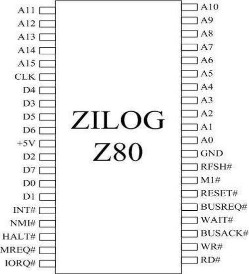
Table 1 Zabogs Z80 internal microprocessor registers
Register Size DescriptionA, A '8-bit Accumulator Donets an operand or operation an operationF, F 'An 8-bit flag keeps the flag or the operation of the ALUB, B 'Versatile 8-bit Can be used alone or as a 16-bit register with CC, C 'Versatile 8-bit Can be used alone or as a 16-bit register with BD, D 'Versatile 8-bit Can be used alone or as a 16-bit register with EE, E 'Versatile 8-bit Can be used alone or as a 16-bit register with DH, H 'Versatile 8-bit Can be used alone or as a 16-bit register with LL, L 'Versatile 8-bit Can be used alone or as a 16-bit register with HI Register 8-bit interrupt Save eight bits of high memory address for processing of vectored interruptsR Register refresh 8-bit Provides a refresh of invisible dinasmic memory by the user. It is automatically incremented and placed on the address channel during each instruction retrieval cycleIX Register 8-bit index Used in indexed addressingIY Register 8-bit index Used in indexed addressingSP 8-bit Stack Push Holds the address of the top stack. See Push or Pop instructionsPC The 8-bit Program Counter Holds the address of the next instructionIFF1 - IFF2 Enable 8-bit Interrupts Set or reset to show interrupt statusIMFa - IMFb 8-bit Interrupt Mode Describes interrupt mode
Table 2 Flip-flop conditions
Action IFF1 IFF2 Comments
Reset CPU 0 0 Disable maskable interruption INT #
Execution IN IN 0 0 Disable interrupt maskable INT #
Execution of EI 1 1 Enable interruption maskable INT #
Execution of LD A, t o o IFF2 => Parity flag
Execution of LD A, R o o IFF2 => Parity flag
Receive NMI # 0 o Disable maskable interruption INT #
Execution of RETN instruction IFF2 o IFF2 => IFF1 as a complement to a NMI service routine #
A0 - A15. Bus Address (output, active High, 3-state). A0 - A15 forms a 16-bit address bus. The Address bus provides an address for the exchange of data bus memory (up to 64Kbyte) and for the exchange of I / O devices.BUSACK #. Bus Notice (output, Low active). The Bus notification shows on the device requesting that the CPU address bus, and MREQ #, IORQ #, RD #, and WR # control signals have entered a high-impedance state. External circuits can now control these paths.BUSREQ #. Bus Request (input, active Low). Bus demand has a higher priority compared to NMI # and is always recognized at the end of the current machine cycle. BUSREQ # forces the CPU address bus, data bus and control signals MREQ #, IORQ #, RD # and WR # to high impedance state so that other devices can control those paths. BUSREQ # normally connected OR (wired-OR) and requires an external pullup resistor for the application. Expansion of the BUSREQ # period due to extensive DMA operations can keep the CPU from refreshing the correct dynamic RAM.D0 - D7. Bus Data (input / output, active High, 3-state). D0 - D7 creates an 8-bit bidirectional data bus, which is used for data exchange with memory and I / O.HALT #. Stop State (Halt) (output, Low active). HALT # indicates that the CPU has executed the Halt command and is waiting for a non-maskable or maskable interrupt before the operation can resume. When stopped, the CPU executes the NOP to keep the memory refresh.INT #. Interrupt Request (input, active Low). Interrupt request is generated by I / O device. The CPU receives an interrupt at the end of the running instruction if the internal software controlled interrupt activation flip (IFF) is enabled. INT # is normally connected with OR and requires an external pullup resistor for those applications.IORQ #. Input / Output Request (output, active Low, 3-state). IORQ # indicates that half the low address bus holds a valid I / O address for a write operation or an I / O readout. IORQ # is also generated simultaneously with M1 # during an interrupt notification cycle to indicate that an interrupt response vector can be placed on the data bus.M1 #. Machine Cycle (output, Low active). M1 #, together with MREQ #, indicates that the current machine cycle is an opcode capture cycle of an instruction execution. M1 #, together with IORQ # indicates that the interrupt notification cycle.MREQ #. Memory Request (output, active Low, 3-state). MREQ # indicates that the address bus holds a valid address for memory readout operations or memory writing.NMI #. Non-Maskable Interrupts (input, triggered negative edge). NMI # has a higher priority than INT #. NMI # is always recognized at the end of the running instruction, independent of the interrupt enable flip-flop state, and automatically forcing the CPU to restart at 0066H.RD #. Read (output, active Low, 3-state). RD # indicates that the CPU wants to read data from memory or I / O devices. I / O devices or addressed memories will use this signal to place data into the CPU data bus.RESET #. Reset (input, active Low). RESET # starts the CPU as follows: resets the interrupt activation flip-flop, erases PC and registers I and R, sets the interrupt status to Mode 0. During reset time, address bus and data are high impedance, and all output control signals Become inactive. Note that RESET # must be active for at least three full clock cycles before complete reset operation.RFSH #. Refresh (output, active Low). RFSH #, together with MREQ # shows the seven bits of the lowest system address bus can be used as a refresher address to the system's dynamic memory.WAIT #. Wait (input, active Low). WAIT # indicates to the CPU that the addressed I / O memory or device is not ready for a data transmission. The CPU then enters a state of waiting for the active signal. The extended WAIT # period can keep the CPU from refreshing the correct dynamic memory.WR #. Write (output, active Low, 3-state). WR # indicates that the CPU data bus holds valid data to be stored on the memory location or the addressed I / O.Instructions Z80The Z80 microprocessor has a bunch of highly versatile and versatile instructions available on some 8-bit microprocessors. It includes unique operations such as block removal for fast and efficient data transfer in memory or between memory and I / O. It also allows multiple bit operations in multiple locations in memory.The Zilog Z80 microprocessor instructions are divided into the following categories:
8-bit loading16-bit loadingExchange, block transfer and search8-bit logic and arithmetic operations
In microprocessor Zi log 80 obtained also memory function and based on the speed of memory there are 4 kinds that is:1. REGISTER MEMORYIs the type of memory where the speed of acces the most rapid, this memory is on the Cpu / processor.Example:Data registers, address registers, stack pointer registers, Memory Address Registers, I / O Address Registers, etc.2. CACHE MEMORYMemory with limited capacity, high speed which is more expensive than the main memory. This memory cache is between the main memory and processing registers, so that the processor does not directly refer to the main memory for performance can be improved.Cache memory there are 2 kinds:1. Cache memory contained in the internal processor, cache memory of this type of accesnya speed is very high, and the price is very mahal.Dapat seen on processors such as P4, P3, AMD-ATHLON dll. The higher the capacity of L1, L2 Cache memory the more expensive and faster the processor.2. Chace memory outside the processor, which is located on the Mother board, this type of memory access speed is very high although not as fast as the first type of memory cache (which is on the internal processor). The bigger the capacity the more expensive and faster. Capacity of chace memory is 256 kb, 512 kb, 1 Mb, 2 Mb etc.3. MAIN MEMORYThis memory serves to store data and programs.The main types of memory are:-Random Access Memory (RAM)Random Access Memory (RAM), or commonly called memory, is a computer tool (hardware / hardware). Ram is one kind of data storage tool on computer or other electronic media (PDA, HP, Notebook, Netbook, etc.) which is temporary. This means that when the computer is turned off, then all instructions or data that have been stored in this ram will be lost. SoThe Ram function is to store a temporary instruction from a computer to eject it into the output device.There are several types of RAM in the market today are SRAM, EDORAM, SDRAM, DDRAM, RDRAM, VGRAM etc.
Components in the microprocessor system can communicate with each other via bus. At the Z-80 microprocessor there are 3 types of buses, ie1. Data bus (data bus)2. Bus address (address bus)3. Bus control (control bus)The data bus on the Z80 microprocessor has 8bit, used to send or receive data between system components. Data bus is a two-way bus because the data bus can receive and send data. The address bus on the Z80 microprocessor is 16bit, so it can contact 64 Kb of memory. This address bus is a one-way bus that is used to send memory location addresses. Bus control on Z80 microprocessor there are 3 types, namely: signal control system, CPU control signal, control signal bus.Microprocessors can work on 8/16/32 bit data. This capability depends on the width of the data path (data bus), while for address delivery depends on the width of the address path it has. The Z-80 microprocessor has 16 address channels which means it can reach 65536 memory locations (64 Kbyte). Each memory location is capable of storing 8 bit data.In the Z80 microprocessor, there is an Arithmatic Logic Unit (ALU) and also a CPU register used to store temporary data. These registers store the count or record to perform a certain operation repeatedly.The instruction sequences are programs stored in memory, streamed through the data bus in sequence, then on the inner bus, to the instruction register. All instructions are examined, and in the system control send signals for control either to the outside or to the microprocessor.The CPU is associated with other parts via the data bus path, address path, and control path. A bus is a number of conductors that function to drain / or channel data out or into the microprocessor. The Z-80 microprocessor has 8 bit register (A, B, C, D, E, H, L, F, I) and is equipped with 16 bit registers of IX, IY, SP, and PC. These registers are used to process and store data temporarily. Register A is used to store data temporarily from the calculation of ALU (Arithmatic Logic Unit). The F register is used to indicate the conditions occurring as a result of arithmetic and logic operations. Register B and C can be used to store cacti. Likewise HL and DE registers are applicable for general purposes.How the microprocessor works is to run a set of machine instructions that tell the processor what to do. Based on these instructions. Microprocessors perform three basic things:1. Use the ALU (Arithmetic logic unit), to perform mammetic operations such as addition, subtraction, multiplication and division. Modern microprocessors contain floating point units that can perform very complex operations on large numbers.2. Move data from one memory location to another3. Make decisions and jump to other instructions according to the decision Simply work the microprossesor is essentially receiving feedback or input commands from the mouse, keyboard or other connected data input device and then translate or process the data command to then release / forward the output to Hardware or related softwareThe workings of a microprocessor are directed by a program in machine-prefixed machine code into a memory.The microprocessor serves as the unit that controls the entire workings of the microprocessor system. Microprocessor functions include the following:Retrieve instructions and data from memory.· Move data to and from memory.· Sending control signals and serving interrupt signals.· Provides timing for the microprocessor system work cycle. Performs logic and arithmetic operations functions.
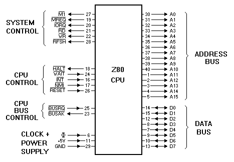
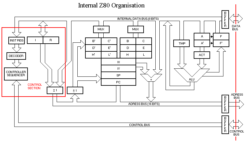

CPU Z80 receives two interrupt input signals: NMI # and INT #. NMI # is a non-maskable interrupt and has the highest priority. INT # is a lower priority interrupt and it is required that this interrupt is enabled through the software to operate. INT # can be connected to varied peripheral devices in OR connected configuration.
Z80 has a single response mode for interrupt service on non-maskable interrupts. The maskable interrupt, INT #, has three programmable response modes available. They are:1.Mode 0 - same as 8080 microprocessor2.Mode 1 - peripheral interrupt service for use with the system instead of 8080 / Z803.Mode 2 - the vectored interrupt scheme, usually daisy-chain, for use with the Z80 family and compatible peripheral devices (compatible).
The CPU serves the interrupt by sampling the signal NMI # and INT # on the rising edge of the last clock of an instruction. Subsequent processing of interrupt services depends on the type of interrupt being detected.
Non-Maskable Interrupt (NMI: Non-Maskable Interrupt). Non-Maskable Interrupts can not be disabled with program control and therefore will be received at any time by the CPU. NMI # is usually reserved only for the highest priority interrupt type service, such as to shutdown after a power failure is detected. After the introduction of NMI signal # (provision of BUSREQ # is off), CPU jumps to location of restart 0066H. Normally, the software starts at that address containing the interrupt service routine.
Maskable Interrupts (INT #). Regardless of the user-set interrupt mode, the CPU responds to maskable interrupt inputs according to a common timing cycle. Once the interrupt is detected by the CPU (it is declared that the interrupt is enabled and BUSREQ # is disabled) a special interrupt processing cycle begins. It starts with a special fetch cycle (M1 #) where IORQ # becomes active while MREQ # is not, as in normal # M1 cycle. In addition, this special M1 # cycle automatically extends to two WAIT states #, to allow for the time required in the interrupt request notification.
Operation Interrupt Mode 0. This mode is the same as interrupt 8080 microprocessor service procedure. The interrupting device places an instruction on the data bus. Normally a Restart instruction, which initiates a call at one location from the eight restart locations selected on the page (page) of zero memory. Unlike 8080, the Z80 CPU responds to Call instructions with only one interruption notification cycle followed by two memory read cycles.
Operation Interrupt Mode 1. Mode 1 operation is very similar to NMI # interrupt. In principle the difference is only one that is interrupt Mode 1 restart (restart) at address 0038H.
Interrupt Mode Operation 2. This interrupt mode has been designed for the use of the highly effective capabilities of the Z80 microprocessor and its relation to peripheral families. The interrupt peripheral device selects the starting address of the interrupt service routine. The device does so by placing an 8-bit vector on the data bus during the interrupt notification cycle. The CPU forms a pointer using this byte as a low 8-bit and the contents of register I as 8-bit high. This pointer shows an entry (entry) in the address table for the interrupt service routine. The CPU then jumps to a routine at that address. Flexibility in the routine address selection of this interrupt service permits peripheral devices; Using several different types of service routines. These routines may be placed on an address in the available memory. Since the interrupt device supplying low-order bytes of a 2-byte vector, bit 0 (A0) must be zero.
Enable / Disable Operation Interrupt. Two flip-flops IFF1 and IFF2, shown in the regression (decryption) register, are used to indicate the status of the CPU interrupt. The two flip-flop operations are depicted in the Table.

A0 - A15. Bus Address (output, active High, 3-state). A0 - A15 forms a 16-bit address bus. The Address bus provides an address for the exchange of data bus memory (up to 64Kbyte) and for the exchange of I / O devices.
BUSACK #. Bus Notice (output, Low active). The Bus notification shows on the device requesting that the CPU address bus, and MREQ #, IORQ #, RD #, and WR # control signals have entered a high-impedance state. External circuits can now control these paths.
BUSREQ #. Bus Request (input, active Low). Bus demand has a higher priority compared to NMI # and is always recognized at the end of the current machine cycle. BUSREQ # forces the CPU address bus, data bus and control signals MREQ #, IORQ #, RD # and WR # to high impedance state so that other devices can control those paths. BUSREQ # normally connected OR (wired-OR) and requires an external pullup resistor for the application. Expansion of the BUSREQ # period due to extensive DMA operations can keep the CPU from refreshing the correct dynamic RAM.
D0 - D7. Bus Data (input / output, active High, 3-state). D0 - D7 creates an 8-bit bidirectional data bus, which is used for data exchange with memory and I / O.
HALT #. Stop State (Halt) (output, Low active). HALT # indicates that the CPU has executed the Halt command and is waiting for a non-maskable or maskable interrupt before the operation can resume. When stopped, the CPU executes the NOP to keep the memory refresh.
INT #. Interrupt Request (input, active Low). Interrupt request is generated by I / O device. The CPU receives an interrupt at the end of the running instruction if the internal software controlled interrupt activation flip (IFF) is enabled. INT # is normally connected with OR and requires an external pullup resistor for those applications.
IORQ #. Input / Output Request (output, active Low, 3-state). IORQ # indicates that half the low address bus holds a valid I / O address for a write operation or an I / O readout. IORQ # is also generated simultaneously with M1 # during an interrupt notification cycle to indicate that an interrupt response vector can be placed on the data bus.
M1 #. Machine Cycle (output, Low active). M1 #, together with MREQ #, indicates that the current machine cycle is an opcode capture cycle of an instruction execution. M1 #, together with IORQ # indicates that the interrupt notification cycle.
MREQ #. Memory Request (output, active Low, 3-state). MREQ # indicates that the address bus holds a valid address for memory readout operations or memory writing.
NMI #. Non-Maskable Interrupts (input, triggered negative edge). NMI # has a higher priority than INT #. NMI # is always recognized at the end of running instructions, independent of the interrupt enable flip-flop state, and automatically forcing the CPU to restart at 0066H.
RD #. Read (output, active Low, 3-state). RD # indicates that the CPU wants to read data from memory or I / O devices. I / O devices or addressed memories will use this signal to place data into the CPU data bus.
RESET #. Reset (input, active Low). RESET # starts the CPU as follows: resets the interrupt activation flip-flop, erases PC and registers I and R, sets the interrupt status to Mode 0. During reset time, address bus and data are high impedance, and all output control signals Become inactive. Note that RESET # must be active for at least three full clock cycles before complete reset operation.
RFSH #. Refresh (output, active Low). RFSH #, together with MREQ # shows the seven bits of the lowest system address bus can be used as a refresher address to the system's dynamic memory.
WAIT #. Wait (input, active Low). WAIT # indicates to the CPU that the addressed I / O memory or device is not ready for a data transmission. The CPU then enters a state of waiting for the active signal. The extended WAIT # period can keep the CPU from refreshing the correct dynamic memory.
WR #. Write (output, active Low, 3-state). WR # indicates that the CPU data bus holds valid data to be stored on the memory location or the addressed I / O.
|
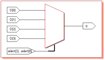


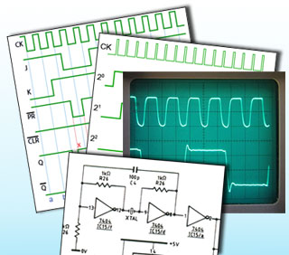

")


Tidak ada komentar:
Posting Komentar