
X . I
glance overview of optoelectronics


Opto-electronics is an application electronic device that functions to detect and control the light source or can also be regarded as a modifier of power equipment to optical or vice versa. The light source used in this application is generated from photodiode injection include diodes, LEDs, and lasers. Some of these sources have been widely used in several optoelectronic devices used in telecommunications fiber optics.
Optoelectronics is a branch of science that involves the field of technology components, tools, and systems that work by modifying the optical properties of a material with an electrical field. So science is studying the interaction between electromagnetism properties (optical) and electrical properties (electrons) of an object.
Knowledge learned from Opto-electronics:
I . lasers and optical amplifiers
II. optical radiation and reinforcement
III. fiber optic sensors
IIII. supervising modulator wave direction
Definition, Functions, and Principles of Optical Fiber :
understanding fiber optics
is glass and plastic tube that is capable of transmitting light, then converted into sound, speech or information. Fiber optic comprising the field related to the study and application of fiber optics technology. Fiber optic cable is also known as the fiber optic cable. These cables use light pulses to carry and transmit data from point to point. Fiber optic cable can transmit data and signals at higher bandwidth and at a faster pace than the traditional copper or aluminum cable lines. It can be used in a variety of data transmission applications.
It's hard to say exactly when the first modern fiber optic cable there and who the inventor of fiber optics. What is known, for sure, is that the first demonstration of the refraction of light guided conducted by Jacques Babinet and Daniel Colladon in 1840. This demonstration provides all the basic principles of fiber optics will be built later.
Fiber optic functions are meant to guide light waves in one direction through the refraction of light. Basically, fiber optic cables transmit light waves from one point to another physical capture and reflect light in the cable back into every time he tries to escape. This makes fiber optic cables are sort of like a prism from which light waves can not escape. The only place for light waves to go, then, is the tip of the fiber optic cable.
working principle Fiber optics is the name for the process by which data is transferred via pulses of light, which is sent through thin strands of glass or plastic. This sort of strands of glass or plastic, also called optical cables, as thin as a human hair, which means many of them can be tied together. It also means they can be damaged very easily.Light waves do not "bend" by themselves, they can not go around the corner without bouncing off a mirror or other reflective surfaces. Fiber optic bend light by "bouncing" light pulses along the wall wiring. This is called total internal reflection. These pulses of light, full of data, can travel quickly over great distances.A transmitter at one end of the fiber optic systems transmit data by converting electronic signals into pulses of light, which is emitted into the fibers. A receiver at the other end receives and decodes the pulses, transforming into an electrical signal, which is then sent to a television, computer and other electronic devices. Sometimes, re - generator necessary to increase the strength of the light signals over very long distances.


.jpg)
X . II
reviews photoelectric effect
The photoelectric effect is the removal of electrons from a surface (usually metallic) when subjected to, and absorbing, electromagnetic radiation (such as visible light and ultraviolet radiation) that is above the threshold frequency depending on the type of surface. Long term for the photoelectric effect is the effect of Hertz (which is currently not used anymore). Hertz observe and then show that the electrode is illuminated with ultraviolet light creates electrical sparks easier.
The photoelectric effect requires photons with energies of several electron volts to over 1 Me V high atomic number elements. The study of the photoelectric effect led to important steps in understanding the quantum nature of light, the electrons and affect the formation of the concept of wave-particle duality. a phenomenon in which light affects the movement of electric charges including photo conductive effect (also known as photo conductivity or photo resistivity), the photo voltaic effect, and photo electro chemical effects.


mechanisms EmissionsPhotons of light have energy characteristics determined by the frequency of light. In the photo emission process, if the electrons in some materials absorb the energy of a single photon and thus have more energy than the work function (the electron binding energy) of the material, it is issued. If the photon energy is too low, the electrons can not get out of the material. Increasing the intensity of the light increases the number of photons in the beam, and thus increase the number of electrons, but it does not increase the energy of each electron is at disposal. The energy of the emitted electrons does not depend on the intensity of incoming light, but only on the energy or the frequency of individual photons. It is the interaction between photons and the outer electrons.Electrons can absorb energy from photons when irradiated, but they usually follow the principle of "all or nothing". All the energy of the photons to be absorbed and used to liberate one electron from atomic binding, or energy radiated back. If the photon energy is absorbed, some of the energy liberates electrons from the atoms, and the remainder was contributed to the kinetic energy of the electrons as free particles.No electrons released by radiation below the threshold frequency, because the electrons do not get enough energy to overcome the bonding of atoms. The emitted electrons are usually called photo electron .
The photoelectric effect helped to guide the wave-particle, where the physics system (such as photons in this case) can demonstrate both properties and behaviors such as wave and like-particle, a concept that is widely used by the creators of quantum mechanics. The photoelectric effect described mathematically by Albert Einstein extending quantum developed by Max Planck.
Photoelectric emission laws:
1. For certain metals and radiation, the number of photo electrons released is proportional to the intensity of light in use.
2. For certain metals, there is a minimum frequency radiation. below this frequency can not be emitted photo electrons.
3. On top of these frequencies, the kinetic energy of the emitted photo electrons does not depend on the intensity of the light, but depending on the frequency of light.
4. The time difference of radiation and photo electron emission is very small, less than 10 ^ -9 sec.
Three steps modelsIn the X-ray regime, photoelectric-effect in the crystalline material is often decomposed into three steps:1. Inner photoelectric effect. The hole left behind can cause effects auger, which is visible even when the electrons do not leave material. Photons in solids molecules are excited in this step and can be seen as a line in the final electron energy. The inner dipole photo effect has to be allowed. The inner photo effect should dipole allowed. The rules for atomic transitions translate through tight binding to crystal models. They are similar in geometry to plasma oscillations in that they must be trans versal.2. Ballistic transport of electrons to the surface of the half. Some electrons are scattered. Some of the scattered electrons.3. The electrons escape from the material on the surface.In the model of three steps, the electron can take multiple paths through three steps. All roads can disrupt the path integral formulation sense. To state the surface and the molecular model of the three steps if it still makes sense even some as the most atoms have electrons that can spread some electrons leave.
X . III
Photodetector
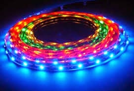
Photo Detector is a tool to measure the intensity of light. Photo
detectors can be divided into three different categories according to
function as: semiconductor-based photo detectors, photo multiplier tubes,
and bolo meters. Semiconductor photo detectors by far the most commonly used in everyday life. Examples are photo diodes that sits in a photo cell to monitor or
Power Button and sensor images and videos used in digital cameras
(usually from C C D - or C MOS -type).
The
main characteristics of the photo detector between judgments is the
level of responsiveness, the level of sensitivity and quantum efficiency
(Bart J. Van Zegh broeck, 1996). Responsiveness
photo detector is defined as the ratio of the current at the
photo detector to the incoming optical power on the device. Sensitivity is defined as the minimum input power that can still be detected by the device. And
the quantum efficiency is defined as the ratio of the number of
electron-hole pairs which generate an electric current to the number of
photons striking the device. Just
as solar cells, photo detector is comprised of various structures, such
as p-n junction, junction p-i-n, as well as the junction of M-S.
photo diodaLight sensitive diode is a type of diode that serves to detection light. Unlike the ordinary diodes, electronic components will change into an electric current. The
light that can be detected by these light-sensitive diodes ranging from
infrared light, visible light, ultra violet to X-rays. Light-sensitive
diode applications ranging from vehicles on public roads counters
automatically, the light meter on a camera as well as some of the
medical equipment field. Tool similar to sensitive diode is a photo transistor (photo transistor). This photo transistor is basically a type of bipolar transistor using the contact (junction) base-collector to receive light. This component has a greater sensitivity than the light-sensitive diodes. This
is because the electrons generated by the photons of light at this
junction is injected at the base and reinforced at the collector. However, the response time of the photo transistors will generally be slower than the light-sensitive diodes.
The working principle photo diode
Photo diodes made of a semiconductor with a popular material is silicon (Si) or gallium arsenide (GaAs), and others include In Sb, In As, Pb Se. This material absorbs light with wavelength characteristics include: 2500 Å - 11000 Å of silicon, 8000 Å - 20,000 Å for GaAs. When a photon (a unit of energy in the light) from the light source is absorbed, it generates a pair of electrons and produce a single charge carriers, an electron and a hole, in which a hole is part of a semiconductor lattice loses electrons. Direction of current through a semiconductor is opposite to the charge carrier movement. The manner in a photo diode is used to collect photons - causes the charge carriers (such as current or voltage) flows / formed in parts of the electrode.
X . IIII
24 words in relation to understanding the opto electronics
optoelectronicsOpto - electronics is the branch of science that examines electronic equipment associated with light and considered to be a sub-field of photo nics.24 relationship: Bit, Light, Diode, light beam, Electromagnetism, Electronics, photo diode, Foton, photonics , Infrared, Laser, Electric, Human Eye, Optics, Fiber optics, beam gamma, X-rays, spectrum, electromagnetic spectrum, the visible spectrum, Technology, Telecommunications, Ultraviolet.beetBit refers to a digit in a binary numeral system (base 2).LightElectromagnetic waves can be described as two waves that propagate transversely in two areas, namely perpendicular magnetic field and electric field. Wave climbed magnet will push electric waves, and vice versa, when the vines, the electric wave will push magnetic waves. The diagram above shows the light waves propagating from left to right with the electric field in the vertical plane and the magnetic field on the horizontal plane. The electromagnetic waves that form of electromagnetic radiation. Light is a form of electromagnetic wave energy that is invisible to the eye with a wavelength of about 380-750 nm.diodeVarious semiconductor diodes, rectifier bottom is bridge structure of vacuum tube diode Diode is an active component of the two poles which are generally semiconductors, which allow electric current to flow in one direction (forward down-payment condition) and inhibits the flow in the opposite direction (down-payment condition backwards).Diode light beamDiode LED light beam (English: light-emitting diode; LED) is a semiconductor that emits incoherent monochromatic light when given a forward voltage.electromagnetismThe electromagnetic field that arises in the solenoid coil Electromagnetism is a branch of physics of electromagnetic fields to learn about electrical fields and magnetic fields.ElectronicElectronics is a tool created by the principles of electronics as well as things or objects that use these tools and, among others, can be used on.photodiodeA photo diode photo diode is a type of diode that serves to detect light.FotonPhotons are the elementary particles in electromagnetic phenomena.photonicsPhotonics is a field of science and research relating to the optics and optical engineering, particularly those associated with particles of photons in the electromagnetic spectrum.InfraredImage of a small dog taken in infrared light-middle (the color of) Infrared is electromagnetic radiation of a wavelength longer than visible light, but shorter than radio wave radiation.LaserLaser (an abbreviation of the English language: Light Amplification by Stimulated Emission of Radiation) is a mechanism of a device that emits electromagnetic radiation, usually in the form of light that can not be seen and can be seen with normal eyes, through stimulated emission process.electricityLightning is an example of the most dramatic natural power Electricity is a series of physical phenomena associated with the presence and flow of electric charge.HumanTwo little boy. Human or person can be interpreted different in terms of biological, spiritual, and cultural terms, or in a mixture.EyeEyes are organs of vision that detect light.OpticsTable Opticks, 1728 '' Cyclopaedia '' Optics is the branch of physics that describes the behavior and properties of light and the interaction of light with matter.optical fiberOptical fiber. Fiber optics is a transmission line or similar cables made of glass or plastic is very smooth and smaller than a strand of hair, and can be used to transmit light signals from one place to another.gamma raysGamma rays gamma rays (often denoted by the Greek letter gamma, γ) are an energetic form of electromagnetic radiation produced by radioactivity or nuclear or subatomic processes such as electron-positron annihilation.X-rayRöntgen. X-rays or Röntgen rays are a form of electromagnetic radiation with a wavelength range of 10 nanometers to 100 picometre (equal to the frequency in the range of 30 petahertz - 30 exahertz) and have energy in the range of 100 eV - 100 Kev.SpectrumThe light spectrum of a rainbow / rainbow spectrum is a state or a price that is not limited to a set price alone but can be changed infinitely within a continuum.electromagnetic spectrumThe electromagnetic spectrum is the range of all possible electromagnetic radiation.The visible spectrumApproximation spectrum of white light transmitted through a "Edmund Scientific "
X . IIIII
Fiber Communication System / Fiber Optic
optic source

optical wave guides Amplifier optic
The development of telecommunications technology allows the delivery of telecommunications facilities in a relatively low cost, high service quality, fast, safe, and also a large capacity indistribute information. Along with the rapid development of the ability of telecommunications transmission system using fiber optic technology are increasingly being developed, so as to shift the use of a conventional transmission system in the future, especially for long distance transmission.The impact of these technological developments is the change in analog networks into digital networks in both the switching system or in the transmission system. This will improve the quality and quantity of information sent, as well as operation and maintenance costs are more economical. As a means of transmission in digital networks, optical fiber acts as a guiding light waves. Optical fiber from glass or silica material with a small size and very light can transmit large amounts of information with relatively low losses.In optical fiber communication system, the information is converted into an optical signal (light) using an LED light source or laser diode. Then the legal basis total reflection, the optical signal containing the information is passed along the fiber to the receiver, then the optical detector will change the optical signals back into electrical signals.
Basic Principles of Optical Fiber Communication Systems1. DriverServes to control the optical sources based on the electrical signals
received and transform electric signals into optical signals.2. Source Optics (Light)Can use LED or LASER. LED is a device that emits light with the direction of spread. It is generally used for step-index multi mode optical fiber. LASER can emit light with a power of 10-100 times greater than the LED. It is generally used for step index single mode optical fiber. For long distance transmission, the use of LASER as a light source is more advantageous than using L E Ds.3. Optical DetectorServes to convert optical signals back into electrical signals. Optical detectors can generate waves in the original, to minimize the
losses incurred during propagation, so it can also generate an
electrical signal with a maximum optical power is small.Optical detectors are often used No 2, namely:a. Optical Detectors PIN (Positive Intrinsic Negative) Photo diodePIN diode is a semiconductor with on dop section P, an intrinsic part on dop N, thus as follows a pat raises a single electron pair of the
absorbedThese detectors work by modulating the function of light absorbed by
the current, where the incoming optical power during a pulse can
considered as acceptance of the number of photons that brackish-each of
which has an energy of:where: H = Planck's constant (6.0625. 10-34)V = velocity photon (C /?)E = energy photonsb. Optical detector A P D (Avalanche Photo diode)Can produce more than one pair of single electrons through ionization. P P E is used for systems that require high sensitivity, while the PIN is used for systems that require low sensitivity.4. The amplifier circuitServes to amplify electrical signals corresponding to the electrical signal is transmitted.
HISTORY AND DEVELOPMENT OF FIBER OPTIC TECHNOLOGY
Of telecommunications theory in mind that using a higher frequency band width will get bigger so that the distribution capacity will also increase further. Based on this theory carried out research into the use of light for communications.a. In 1960, Maiman of Hunges Aircraft find LASER (Light Amplification by Stimulated Emission of Radiation ), then the thought of using light as a communication tool.b. LASER beam due to its characteristics, can be required together with such electromagnetic waves and pretty well used to distribute information.c. Laser was first tried as a means of communication by means of light emitting into the air, but this experiment failed because of interference such as rain, wind, snow, etc. so that similar experiments were never performed again.d. Subsequent experiments performed by emitting laser beam into BEAM GUIDE (pipe) is incorporating a lens at a certain distance, the lens serves to focus the laser beam coming.From the results of this experiment turns out, losses in transmission as in item [c] above can be minimized, but the accuracy of the location of the lens along the BEAM GUIDE should be kept, because if there is a change or shift in the location of the lens (due to impact or vibration) will interfere with the propagation of the Laser Beam the.Communication in this way, is not used anymore because it is impractical and costly.e. Of the various types of laser (Laser solid, liquid and semi-conductor), the type of semi-conductor laser is best, although the short operational lifespan.f. In 1966, DR KAO experimenting with laser beams propagate into Transparent Fiber. But the only successful way for relatively short distances. This was due to less than perfect the manufacturing process Transparent Fiber, causing losses of materials that can hinder the process of light propagation therein.g. In 1970, Cording glass factory in the United States managed to create a fiber with a silica base material that has material losses are relatively small (± 20 dB / km), so it is best used for light communications.h. At the same time found with silica as a base material fiber, the operational life semiconductor lasers was successfully increased to 10,000 hours (by Hayashi and Panish).i. In addition to semiconductor lasers, developed another optical source in called LED. Similarly, the laser can emit light very well, but in the absence of feedback on the light in emission or entered on the fiber, the LED produces light that is not coherent.LEDs can emit rays in several different modes so only suitable for multi mode optical fiber with a large diameter.j. On the receiver side (Detectors), Johnson found Photo Diode which can amplify the signal comes and Avalanche Photo Diode (APD) is still an underdog optical detector.k. In 1976, trials conducted using an optical cable to the network connector (junction), but the result is quite good, so that in the subsequent years its use began to be promoted widely.l. In 1980, the United States and Spain have been using an optical cable as a means of rural telecommunications (Rural Telecommunication).m. In 1983, after the optical fiber developed and produced by many countries and its widespread use began, Japan and the United States work together to build the transmission system connecting Japan-Hawaii (along 7000 km) by using an optical cable.
CHARACTERISTICS OF OPTICAL FIBERa. Small sizeThe outer diameter of an optical fiber ranges between 100-250 lm. Maximum Diameter after coated / wrapped plastic / nylon as a jacket to ± 1 mm. This size is still very small compared with the conductor coaxial cable (1- 10 mm).b. LightCompared with ordinary transmission cable (Spesific gravity 9.8) then specific gravity silica material as the optical fiber is 2.2, so that the weight becomes 1/2 - 1/3 the weight of an ordinary transmission cable.c. litheIn general, the optical fiber will not be broken when it is curved with a radius of 5mm. Therefore, fiber optic cables have the same flexibility with ordinary transmission cable, so the technical installation is not much different from regular cable installation techniques.d. not rustySilica material as the base material of optical fiber has a very stable chemical properties therefore unlikely to be corroded.e. Low lossesSilica optical fiber with a material having a low transmission loss, the amount of about 2-8 dB / km at a wavelength of 830 nm. Compared to coaxial cables that have a transmission loss of 19 dB / km at a frequency of 60 Mhz.f. high capacityCapacity to distribute information per area of very large cross section in addition to having a wide bandwidth (broadband). For example: Capacity distribution per cross section area of 100 x compared
with multi-pair cable and 10 x compared to coaxial cable.g. free inductionOptical fiber using silica base material which is basically a very good dielectric material and immune to electromagnetic induction, and also against lightning / thunder.h. Low Cross TalkThe possibility of leakage of light between optical fibers are very small, as well as leakage due to the influx of light from the outside and then go propagating in optical fibers.i. High temperature resistanceSilica materials have got ± 1900º C melting point and is very far above the melting point and plastic capper. Is ideal when used as a means of communication in areas that are prone to high temperatures.j. No cause sparksAt the point of connection is not possible sparks (discharge), therefore it is ideal when used in places that are sensitive to explosion / fire.k. Unable branchedFiber optics have a very small size / very thin. Therefore it becomes difficult if not impossible to branched. When you have branched it must be done in advance of a change in the optical signal to an electrical signal.l. Not using copperOptical fiber using silica materials that do not contain metal elements even optical fibers using Multi component Glass, element alloys (copper) is very small. Copper protector only used as a coating on the fiber optic cable for communication submarine cables and as the passage of DC current to voltage at the dole-repeater repeater under the sea.m. FragileAlthough fragile, yet still has the power stretch approximately 5% to avoid damage to the optical fibers at the time of installation / withdrawal, then when compiled into a fiber optic cable by the amplifier.
BASIC STRUCTURE OF OPTICAL FIBERThe basic structure of the optical fiber is actually composed of coating, cladding and core. However, for security reasons then added a safety after the coating layer. The coating can be a plastic, zinc, or iron woven wire depending on the condition of the optical cable is placed. Here is a picture of the composition of the optical fiber.The basic structure of the optical fiber> Core (Core)Core functions to determine the light propagates from one end to the other. Core made of quartz with very high quality. There is also made from the mixture of silica and glass. As the core, the core also his vines light spot on the optical fiber. Has a diameter of 10 μm - 50 lm. Core size affect the characteristics of the optical fiber.> CladdingCladding serves as a mirror that reflects light in order to propagate to the other. Given this cladding light can propagate in fiber optic core. Cladding made of glass materials with a refractive index that is smaller than the core. Cladding is the sheath of the core. Cladding diameter between 5 μm - 250 lm. The relationship between the refractive index of core and cladding would affect the propagation of light in the core (influences the critical angle).> Coating (Jackets)Serves as a protective coating on the fiber optic mechanical and color coded identity. Made of plastic. Serves to protect the optical fiber from damage.
foundation of thought BASIC FIBRE OPTIC
Optical fiber communication systems related to energy propagation of light in optical fibers. How optical fibers passing the light depends on the nature of light and the structure of the optical fiber telecommunication dilewati.Dari viewpoint, light is a form of energy that travels in waves. That is, the optical fiber is also called an optical waveguide, because it serves as a guide light waves.Parameter sustu light of the material you need to know is the index of refraction or refractive index. When light waves propagate in a vacuum, the speed is c = 3 × 10⁸ m / s. When the light wave propagates through the material, not in a vacuum, then the speed will be lower than in a vacuum, that is equal to:v = c / n or n = c / vwhere n = index of refraction or refractive indexv = speed of light inside the materialLight travels in two different mediums in three ways: straight vines, refracted and reflected. When light crosses two different media, there is a part of the light reflected back into the first medium and the other part is refracted.TYPES OF FIBRE OPTICOptical fiber consists of several types, namely:1. Step Index MultimodeIn this type of multimode step index, core diameter greater than the diameter cladding. The impact of the magnitude of the core diameter dispersion caused losses transmitnya great time. The addition of silica material percentage at the time of manufacture. Not too influential in reducing the losses dispersion transmit time. Here is a picture of wave propagation in a step index multimode optical fiber.Wave Propagation in Step Index Multi modeThis type of optical fiber has a refractive index that sudden changes as shown by the following figure.Refractive index of the multi mode step indexStep Index Multi mode has the following characteristics:• constant core refractive index.• large core size (50mm) and coated with a very thin cladding.• The connection cable is easier because it has a large core.• Frequent dispersion.• Only used for short distances and low bit rate data transmission.2. Graded Index Multi modeOn what kind of graded index multi mode optical fiber is. Core consists of a number of layers of glass that have different refractive indices, the refractive index is highest at the center of the core and gradually decreases to a core-cladding boundary. As a result of the various mode dispersion of light that propagates is reduced so that the light will arrive on time coincide . Here is a picture of wave propagation in multi mode graded index.
Wave Propagation in Graded Index MultimodeRefractive index that changes slowly is shown in the following figure.
Changes in the refractive index multi mode graded indexMulti mode Graded Index has the following characteristics:• Light travels due to diffraction that occurs in the core so that the propagation of light parallel to the fiber axis.• Dispersion minimum so good if it is used for medium range• The size of between 30 μm core diameter - 60 lm. smaller than multi mode step-index and made of silica glass.• The price is higher than Step Index Multi mode optical fiber due to the manufacturing process more difficult.3. Single Step mode IndexIn single mode step index type. Both core and at cladding made of silica glass. Size core is much smaller than the cladding is made so in order to reduce transmission losses due to fading. As shown in the following figure.Wave Propagation in Single mode Step IndexIn this single mode step index. Refractive index changes abruptly as the multi mode step index. As shown in the following figure.Index bias for the single mode step indexSingle mode Step Index has the following characteristics:• Single mode Step Index Fiber optics have a core diameter is very small compared his cladding size.• The size of between 2 μm core diameter - 10μm.• Light only travels in one mode only that is parallel to the axis of the optical fiber.• Has a very small damping.• Have a wide bandwidth.• Used for data transmission with a high bit rate.• Can be used for short distance transmission, intermediate and far.For this type of single mode there are some specifications that are commonly used. Ie G652, G653, G665, G662
Changes in the refractive index multi mode graded indexMulti mode Graded Index has the following characteristics:• Light travels due to diffraction that occurs in the core so that the propagation of light parallel to the fiber axis.• Dispersion minimum so good if it is used for medium range• The size of between 30 μm core diameter - 60 lm. smaller than multi mode step-index and made of silica glass.• The price is higher than Step Index Multi mode optical fiber due to the manufacturing process more difficult.3. Single Step mode IndexIn single mode step index type. Both core and at cladding made of silica glass. Size core is much smaller than the cladding is made so in order to reduce transmission losses due to fading. As shown in the following figure.Wave Propagation in Single mode Step IndexIn this single mode step index. Refractive index changes abruptly as the multi mode step index. As shown in the following figure.Index bias for the single mode step indexSingle mode Step Index has the following characteristics:• Single mode Step Index Fiber optics have a core diameter is very small compared his cladding size.• The size of between 2 μm core diameter - 10μm.• Light only travels in one mode only that is parallel to the axis of the optical fiber.• Has a very small damping.• Have a wide bandwidth.• Used for data transmission with a high bit rate.• Can be used for short distance transmission, intermediate and far.For this type of single mode there are some specifications that are commonly used. Ie G652, G653, G665, G662
X . IIIII
WAVE GUIDE SENSORS
Wave guide Sensors : Basic Working Principle
Although trapped within the dielectric medium of the optical wave guide,
the radiation that propagates inside
the wave guide can be perturbed by
the external environment, and this perturbation can be used to draw
useful information for sensing purposes.
In fact, the interaction of the
parameter of interest, that is the me
asurand , with the wave guide produces
a modulation in the propagation constants of the guided light beam. That
modulation represents the sensitive function of the measurand of interest.
As shown in Fig. 4, the basic
elements constituting a guided wave
sensor are: an optical source, an
optical interface for source-to- wave guide light coupling, the wave guide itself where the measurand-
induced light modulation occurs, a photo detector and the electronics for
amplification, signal processing and data display.


Figure . Examples of fiber optic
pressure or vibration sensors based on a mechanical transducer.

Figure . Fiber optic pressure or vibration sensor
based on a micro bending effect
Micro-structured Fiber Sensors
Photonic Crystal Fibers (PCFs)
constitute a class of optical fibers that has a large potential for sensing
applications. Their novel structure, with a lattice of air holes running along
the length of the fiber, offers extraordinary control over the waveguiding
properties in a way that is not possible with conventional fibers.
PCFs are commonly classified by the light-guidance
mechanism in two categories, namely index guiding and photonic band gap (PBG)
fibers (Fig.). In the two types, the microstructured cladding surrounds a
solid and a hollow core, respectively.

Figure . Structure of index guiding (left) and photonic band-gap (right) fibers.
In the index guiding fibers, the refractive index of
the core is higher than the effective refractive index of the cladding and a
modified form of total internal reflection guides the light; in the second type
photonic band gap effect provides guidance, allowing for novel features such as
light confinement to a low-index core.
The PCFs design suggests a variety of strategies for
optical sensing of different physical parameters (temperature, hydrostatic
pressure, elongation, force, bending, etc.). The most studied approach involves
the interaction with an evanescent field of PCF modes for the detection and
analysis of liquid and gas phases species infiltrated in air holes of the
cladding in index-guiding PCF or with a guided field in
hollow core of the PBG fibers. Even if the majority of sensors
reported in literature is based on index guiding fibers, because first
introduced into the market, for sensing applications there are considerable
advantages also in bandgap fibers: one of them is the possibility of guiding
light in hollow cores filled with liquid or gas solutions of molecules.
In a well designed photonic band gap fiber, the largest
part of the mode field (< 90%) is guided in the sample volume, thus
providing a strong interaction between molecules and light over several tens of
centimetres using few microliters of sample. For acetylene
detection with high sensitivity, Ritari et al. investigated the feasibility of using PBG fibers. A
significant interaction between light and molecules in the air holes of the
cladding can take place also in index guiding PCFs, but the effect is smaller
because it concerns only the evanescent field. For evanescent-wave sensing of
biomolecules, such as DNA or proteins, this effect can be
enhanced using index guiding PCFs based on polymers.
A particular advantage of PCF based sensors is the
possibility of writing additional periodic structures on fibers such as Bragg
and Long Period Gratings (LPGs). Standard grating fabrication techniques
applied to PCFs have enabled the fabrication of gratings with original
properties, mainly due to the complex index profile and dispersion properties
of PCFs. From the point of view of fabrication, LPGs are generally easily fabricated,
and can also generate well-isolated resonance, by proper selection of cladding
mode for coupling, that can be highly sensitive to different measurands such as
temperature, bending, strain and external refractive index. In particular for
DNA sensing, this kind of gratings can be employed to detect the average
thickness of a biomolecules layer within a few nm with sensitivity of
approximately 1.4 nm / 1 nm in terms of shift in resonance wavelength per
thickness of DNA layer.
The control of the dispersion properties of core and
cladding can be used, in principle, to increase the sensitivity to one
measurand and to make the device insensitive to another. Recently it has been
reported that LPGs inscribed in a dopant free endlessly single mode (ESM) PCF
and in a large mode area PCF by electric arc discharges eliminate the
crosssensitivity to temperature perturbations.
Another sensing technique makes use of birefringence
in PCFs, which can indeed be made highly birefringent: the large index contrast
facilitates high form birefringence, allowing the development of a new
generation of polarimetric fiber sensors which use polarization (phase)
modulation induced by external perturbations. Different methods have been
developed to introduce birefringence into PCFs, such as using elliptical air
holes and/or asymmetric core or asymmetric distribution of
holes.
An improvement of this sensing technique is represented
by new geometries of cladding holes and, very recently, by the development of
defected solid core.
When the evanescent field sensing method may be
impractical or inconvenient, an improvement is achieved by tapering the fiber.
There are two possibilities during the tapering: the holes structure may be
preserved or may collapse. In both cases the guided mode of the PBG fiber
spreads out, and the tapered PBG fiber results highly sensitive to external
environment. The mechanism is very similar to what happens in tapered
conventional fibers. The collapse of the holes makes the core
mode to couple to multiple modes of the solid taper waist, which is a solid multimode
fiber. Several interference peaks appear from the beating of the multiple modes
of the collapsed region, and they shift as external index changes. The tapering technique has been successfully employed with fibers formed by a
Germanium doped core surrounded by large air holes in the cladding,demonstrating to be of particular interest also for biophotonic sensing.
The optical properties of PCFs are strongly controlled
by the geometry of the holey region, and in sensing application this tunability
is widely employed. One of the most promising advantages of PCF is the
possibility of fabrication of multi-core fibers. A two-core index guiding fiber
bends in the plane containing the two cores, each of them supports a single
guided mode. Because of the bending, the outer and the inner cores undergo an
increase and a reduction in length, respectively. The PCF with these two cores
acts as a two arms Mach-Zehnder interferometer in which the phase difference is
a function of curvature in the plane containing the two cores fiber,
demonstrating a resolution of about 170 μrad/rad.
Important engineering areas can be influenced by
future advances of polarimetric PCF based sensors, in particular thanks to
their direct sensitivity to strain. The best example is the measurement of
axial strain for structural monitoring. The essential mechanisms for strain and
pressure sensing are almost the same: physical changes in fiber dimensions and
the elasto-optic effect. Taking advantage of these two effects, one can
implement distributed sensing elements to assess length changes, internal
stresses or pressure in civil engineering structures. Based on elasto-optical
measurements of the polarization state of the fiber output, it is possible to
determine the fiber birefringence (beat length) for different wavelengths and
compare it with numerical simulations. A new and quite important application of
highly birifringent PCF is in dynamic pressure sensing for tsunami detection,
making use of standard polarimetric technique.
Integrated Optic Sensors
While the basic principles on which
integrated optic sensors (IOSs) are based are the same as for fiber optic
sensors, the two fields have developed at different paces and with slight
different targets.
Fibers have the unique
capability of operating over extended gauge lengths (even km!) in either point
sensing or distributed sensing format. In the former case, the FOS is
configured in such a way that monitoring of the measurand occurs at a specified
location along the fiber (generally at its distal end); in the latter case, the
values of the measurand (e.g. temperature or strain) are probed as a function
of the position along the fiber. Remote measurements are made possible by the
low attenuation characteristic of an optical fiber. Integrated optics (IO), on
the other hand, has been developed with the aim of implementing
multi-functional miniaturized circuits, possibly of size of a few cm, if not
mm.
High-quality fibers, for both telecommunications and
sensing, are mostly made of a silica core (even if, of course, there are
alternative materials, including polymers). IO wave guides can be fabricated in
a variety of materials, from dielectrics to polymers, from liquid crystals to
semiconductors, and none of them has so far emerged as the key material. The lack
of a unique solution for IO in terms of material and fabrication technology,
however, is at the same time its major limit and its greater advantage: it
permits, in fact, very great flexibility both in design and manufacture. Thus,
an IOS may fully exploit the combination of thin films technology with other
planar technologies, such as surface acousto-optic interaction, laser writing,
silicon micromachining, microelectro-mechanical systems (MEMS), optoelectronics
integration on a semiconductor substrate, etc. Since two papers on IOSs, a
temperature and a displacement sensor, respectively, were first published in
1982,many other integrated optical devices for sensing have
been proposed and demonstrated. In the following, some
examples of IOSs will briefly presented and discussed.
Conclusions
Optical waveguide sensors have certain
advantages that include immunity to electromagnetic interference, lightweight,
small size, high sensitivity, large bandwidth, and ease in implementing
multiplexed or distributed sensors.
Strain, temperature and pressure are the most widely
studied measurands for optical fiber sensors, but biomedical applications are
becoming the most interesting area for both fiber and integrated optic sensors.
Nowadays, some success has been gained in the commercialization of optical
waveguide sensors, even if in various fields they still suffer from competition
with other mature sensor technologies.
New ideas, materials and structures, however, are being
continuously developed and tested not only for the traditional measurands but
also for new applications. As an example, we can conceive that further advances
in the fabrication and understanding of microstructured fibers and photonic
crystal structures will provide a platform for new sensors, aiming at being
alternatives for standard sensing technologies.
Brilliant perspectives also exist for new
"smart" optical sensors which mix nanoelectronics and micro/nano
optical devices on the same silicon chip. These fully integrated optosensors
would have the same, or better, characteristics of current sensors, while being
much smaller, lighter and lower power than the existing systems.
optoelectronics and optics


X . IIIIII
Optoelectronics Component Overview
Displays

LED displays present
a somewhat unique set of design constraints and challenges. Instrument
clusters require a certain amount of illumination to be clearly
readable, and, as ambient lighting conditions change, the brightness of
the backlight must be adjusted to compensate. It is essential that the
dimming range of an LED/LED driver system is sufficiently wide to
accomplish this. In addition to being compact and cost-efficient, LED
driver ICs must withstand the harsh thermal, chemical, and electrical
conditions of an automotive environment. Reliable current regulation
over a range of environmental circumstances is critical for maintaining
uniform brightness across the panel and for protecting the long
operating life of an LED backlight.


Fiber Optics
Fiber optics are
flexible, transparent fibers that transmit light between its two ends.
They are used in communications, where transmission over long distances
and higher bandwidths are possible. The extruded glass or plastic fibers
are immune to electromagnetic interference and have less loss than
metal wires.

High Power LEDs
A High Power LED is
an individual component that is greater than 0.20 watts, generally
smaller in package size and finds applications where traditional
lighting sources will not fit.
LED
A LED is
a semiconductor device that emits infrared or visible light when
charged with an electric current. LEDs emit light wavelengths both
visible and invisible when electrically charged. The color emitted is
derived from the chemical composition of the semiconductor material used
in manufacturing. LEDs are differentiated by their color/wavelength
measured in units of nanometers (nm) or their color corrected
temperature (CCT) measured in units of Kelvin (K). In addition, LEDs may
consume lower power, provide longer lifetime, be more robust, and are
able to be switched On/Off at very high rates of speed.

LED Indication
LED indication products
and solutions facilitate machine to human communication. Indication
refers to the use of a light source that is to be viewed directly as a
self-luminous object, such as in signs, signals, and indicator lights on
electronic equipment. LED Indication also includes everything from
mounting hardware to LED Drivers and light pipes, as well as other
useful replacement parts.

Optocoupler/Photocoupler
An optocoupler is
a component that uses a short optical transmission path to transfer a
signal between elements of a circuit, typically a transmitter and a
receiver, while keeping them electrically isolated. An electrical signal
is changed to an optical signal and then back to an electrical signal
therefore breaking the electrical path, i.e. isolating the circuits.
Optocouplers are also known as opto-isolators and photocouplers. Many
systems require signals and data to be transferred from one subsystem to
another within electronics equipment without a direct electrical
connection. Safety agencies require the isolation. Isolation is
necessary when the source and destination circuits are operating at very
different voltage levels. For example: A microprocessor operating at 5V
DC is being used to control a circuit that is switching at 240V DC. The
link between these two circuits is isolated to protect the
microprocessor from overvoltage damage.
X . IIIIIII
X . IIIIIII
Photonics, Electro Optics or Optoelectronics?
The practical uses of the words photonics, electro optics and
optoelectronics often differ from some of their stated definitions. When
looking for a product, job, or literature related to optics and
electronics, listings can appear in what seems an inappropriate place.
It
may be useful in practical situations to ignore the strict distinctions
as defined below, and apply all three terms to obtain more information
than would result from strictly following some stated definitions.
Definitions:
Photonics
Dictionary defines photonics as “the technology for generating and
harnessing light…whose quantum unit is the photon…” Its definition
includes the means for producing, controlling, sensing/detecting light
by optical components and instruments. It does include electro-optical
instrumentation. Photonics is the broadest of the three terms.
Electro-optics
is defined as the “use of applied electrical fields to generate and
control optical radiation. However, it would appear from this
definition, and from others, that it would apply to material changes due
to electric fields such as occur with liquid crystal displays, such as
Kerr & Pockels effects. A warning is provided that “electro-optic
(E-O) is often used erroneously as a synonym for optoelectronic.”
Finally,
optoelectronics is said to pertain “to a device that responds to
optical power, emits or modifies optical radiation or utilizes optical
radiation for its internal operation” or “any device that functions as
an electrical-to-optical or optical-to electrical transducer.”

LED LIGHTING


Infra red optics
 Color sensors
X . IIIIIIII
Optical amplifier
An optical amplifier is a device that amplifies an optical signal directly, without the need to first convert it to an electrical signal. An optical amplifier may be thought of as a laser without an optical cavity, or one in which feedback from the cavity is suppressed. Optical amplifiers are important in optical communication and laser physics.There are several different physical mechanisms that can be used to amplify a light signal, which correspond to the major types of optical amplifiers. In doped fibre amplifiers and bulk lasers, stimulated emission in the amplifier's gain medium causes amplification of incoming light. In semiconductor optical amplifiers (SOAs), electron-hole recombination occurs. In Raman amplifiers, Raman scattering of incoming light with phonons in the lattice of the gain medium produces photons coherent with the incoming photons. Parametric amplifiers use parametric amplification.
 Optical amplifiers are used to create laser guide stars.
 Laser amplifiers
Almost any laser active gain medium can be pumped to produce gain for light at the wavelength of a laser made with the same material as its gain medium. Such amplifiers are commonly used to produce high power laser systems. Special types such as regenerative amplifiers and chirped-pulse amplifiers are used to amplify ultrashort pulses.Doped fibre amplifiers

Schematic diagram of a simple Doped Fibre Amplifier
An erbium-doped waveguide amplifier (EDWA) is an optical amplifier that uses a waveguide to boost an optical signal.
Amplification is achieved by stimulated emission of photons from dopant ions in the doped fibre. The pump laser excites ions into a higher energy from where they can decay via stimulated emission of a photon at the signal wavelength back to a lower energy level. The excited ions can also decay spontaneously (spontaneous emission) or even through nonradiative processes involving interactions with phonons of the glass matrix. These last two decay mechanisms compete with stimulated emission reducing the efficiency of light amplification.
The amplification window of an optical amplifier is the range of optical wavelengths for which the amplifier yields a usable gain. The amplification window is determined by the spectroscopic properties of the dopant ions, the glass structure of the optical fibre, and the wavelength and power of the pump laser.
Although the electronic transitions of an isolated ion are very well defined, broadening of the energy levels occurs when the ions are incorporated into the glass of the optical fibre and thus the amplification window is also broadened. This broadening is both homogeneous (all ions exhibit the same broadened spectrum) and inhomogeneous (different ions in different glass locations exhibit different spectra). Homogeneous broadening arises from the interactions with phonons of the glass, while inhomogeneous broadening is caused by differences in the glass sites where different ions are hosted. Different sites expose ions to different local electric fields, which shifts the energy levels via the Stark effect. In addition, the Stark effect also removes the degeneracy of energy states having the same total angular momentum (specified by the quantum number J). Thus, for example, the trivalent erbium ion (Er+3) has a ground state with J = 15/2, and in the presence of an electric field splits into J + 1/2 = 8 sublevels with slightly different energies. The first excited state has J = 13/2 and therefore a Stark manifold with 7 sublevels. Transitions from the J = 13/2 excited state to the J= 15/2 ground state are responsible for the gain at 1.5 µm wavelength. The gain spectrum of the EDFA has several peaks that are smeared by the above broadening mechanisms. The net result is a very broad spectrum (30 nm in silica, typically). The broad gain-bandwidth of fibre amplifiers make them particularly useful in wavelength-division multiplexed communications systems as a single amplifier can be utilized to amplify all signals being carried on a fibre and whose wavelengths fall within the gain window.
Basic principle of EDFA
A relatively high-powered beam of light is mixed with the input signal using a wavelength selective coupler (WSC). The input signal and the excitation light must be at significantly different wavelengths. The mixed light is guided into a section of fibre with erbium ions included in the core. This high-powered light beam excites the erbium ions to their higher-energy state. When the photons belonging to the signal at a different wavelength from the pump light meet the excited erbium atoms, the erbium atoms give up some of their energy to the signal and return to their lower-energy state. A significant point is that the erbium gives up its energy in the form of additional photons which are exactly in the same phase and direction as the signal being amplified. So the signal is amplified along its direction of travel only. This is not unusual - when an atom “lases” it always gives up its energy in the same direction and phase as the incoming light. Thus all of the additional signal power is guided in the same fibre mode as the incoming signal. There is usually an isolator placed at the output to prevent reflections returning from the attached fibre. Such reflections disrupt amplifier operation and in the extreme case can cause the amplifier to become a laser. The erbium doped amplifier is a high gain amplifier.Noise
The principal source of noise in DFAs is Amplified Spontaneous Emission (ASE), which has a spectrum approximately the same as the gain spectrum of the amplifier. Noise figure in an ideal DFA is 3 dB, while practical amplifiers can have noise figure as large as 6–8 dB.As well as decaying via stimulated emission, electrons in the upper energy level can also decay by spontaneous emission, which occurs at random, depending upon the glass structure and inversion level. Photons are emitted spontaneously in all directions, but a proportion of those will be emitted in a direction that falls within the numerical aperture of the fibre and are thus captured and guided by the fibre. Those photons captured may then interact with other dopant ions, and are thus amplified by stimulated emission. The initial spontaneous emission is therefore amplified in the same manner as the signals, hence the term Amplified Spontaneous Emission. ASE is emitted by the amplifier in both the forward and reverse directions, but only the forward ASE is a direct concern to system performance since that noise will co-propagate with the signal to the receiver where it degrades system performance. Counter-propagating ASE can, however, lead to degradation of the amplifier's performance since the ASE can deplete the inversion level and thereby reduce the gain of the amplifier.
Gain saturation
Gain is achieved in a DFA due to population inversion of the dopant ions. The inversion level of a DFA is set, primarily, by the power of the pump wavelength and the power at the amplified wavelengths. As the signal power increases, or the pump power decreases, the inversion level will reduce and thereby the gain of the amplifier will be reduced. This effect is known as gain saturation – as the signal level increases, the amplifier saturates and cannot produce any more output power, and therefore the gain reduces. Saturation is also commonly known as gain compression.To achieve optimum noise performance DFAs are operated under a significant amount of gain compression (10 dB typically), since that reduces the rate of spontaneous emission, thereby reducing ASE. Another advantage of operating the DFA in the gain saturation region is that small fluctuations in the input signal power are reduced in the output amplified signal: smaller input signal powers experience larger (less saturated) gain, while larger input powers see less gain.
The leading edge of the pulse is amplified, until the saturation energy of the gain medium is reached. In some condition, the width (FWHM) of the pulse is reduced.[2]
Inhomogeneous broadening effects
Due to the inhomogeneous portion of the linewidth broadening of the dopant ions, the gain spectrum has an inhomogeneous component and gain saturation occurs, to a small extent, in an inhomogeneous manner. This effect is known as spectral hole burning because a high power signal at one wavelength can 'burn' a hole in the gain for wavelengths close to that signal by saturation of the inhomogeneously broadened ions. Spectral holes vary in width depending on the characteristics of the optical fibre in question and the power of the burning signal, but are typically less than 1 nm at the short wavelength end of the C-band, and a few nm at the long wavelength end of the C-band. The depth of the holes are very small, though, making it difficult to observe in practice.Polarization effects
Although the DFA is essentially a polarization independent amplifier, a small proportion of the dopant ions interact preferentially with certain polarizations and a small dependence on the polarization of the input signal may occur (typically < 0.5 dB). This is called Polarization Dependent Gain (PDG). The absorption and emission cross sections of the ions can be modeled as ellipsoids with the major axes aligned at random in all directions in different glass sites. The random distribution of the orientation of the ellipsoids in a glass produces a macroscopically isotropic medium, but a strong pump laser induces an anisotropic distribution by selectively exciting those ions that are more aligned with the optical field vector of the pump. Also, those excited ions aligned with the signal field produce more stimulated emission. The change in gain is thus dependent on the alignment of the polarizations of the pump and signal lasers – i.e. whether the two lasers are interacting with the same sub-set of dopant ions or not. In an ideal doped fibre without birefringence, the PDG would be inconveniently large. Fortunately, in optical fibres small amounts of birefringence are always present and, furthermore, the fast and slow axes vary randomly along the fibre length. A typical DFA has several tens of meters, long enough to already show this randomness of the birefringence axes. These two combined effects (which in transmission fibres give rise to polarization mode dispersion) produce a misalignment of the relative polarizations of the signal and pump lasers along the fibre, thus tending to average out the PDG. The result is that PDG is very difficult to observe in a single amplifier (but is noticeable in links with several cascaded amplifiers).Erbium-doped optical fibre amplifiers
The erbium-doped fibre amplifier (EDFA) is the most deployed fibre amplifier as its amplification window coincides with the third transmission window of silica-based optical fibre.Two bands have developed in the third transmission window – the Conventional, or C-band, from approximately 1525 nm – 1565 nm, and the Long, or L-band, from approximately 1570 nm to 1610 nm. Both of these bands can be amplified by EDFAs, but it is normal to use two different amplifiers, each optimized for one of the bands.
The principal difference between C- and L-band amplifiers is that a longer length of doped fibre is used in L-band amplifiers. The longer length of fibre allows a lower inversion level to be used, thereby giving at longer wavelengths (due to the band-structure of Erbium in silica) while still providing a useful amount of gain.
EDFAs have two commonly used pumping bands – 980 nm and 1480 nm. The 980 nm band has a higher absorption cross-section and is generally used where low-noise performance is required. The absorption band is relatively narrow and so wavelength stabilised laser sources are typically needed. The 1480 nm band has a lower, but broader, absorption cross-section and is generally used for higher power amplifiers. A combination of 980 nm and 1480 nm pumping is generally utilised in amplifiers.
The optical fibre amplifier was invented by H. J. Shaw and Michel Digonnet at Stanford University, California, in the early 1980s . The EDFA was first demonstrated several years later by a group including David N. Payne, R. Mears, I.M Jauncey and L. Reekie, from the University of Southampton in collaboration with a group from AT&T Bell Laboratories, E. Desurvire, P. Becker, and J. Simpson and the Italian Company Pirelli . The dual-stage optical amplifier which enabled Dense Wave Division Multiplexing (DWDM,) was invented by Stephen B. Alexander at Ciena Corporation.
Doped fibre amplifiers for other wavelength ranges
Thulium doped fibre amplifiers have been used in the S-band (1450–1490 nm) and Praseodymium doped amplifiers in the 1300 nm region. However, those regions have not seen any significant commercial use so far and so those amplifiers have not been the subject of as much development as the EDFA. However, Ytterbium doped fibre lasers and amplifiers, operating near 1 micrometre wavelength, have many applications in industrial processing of materials, as these devices can be made with extremely high output power (tens of kilowatts).Semiconductor optical amplifier
Semiconductor optical amplifiers (SOAs) are amplifiers which use a semiconductor to provide the gain medium. These amplifiers have a similar structure to Fabry–Pérot laser diodes but with anti-reflection design elements at the end faces. Recent designs include anti-reflective coatings and tilted wave guide and window regions which can reduce end face reflection to less than 0.001%. Since this creates a loss of power from the cavity which is greater than the gain, it prevents the amplifier from acting as a laser. Another type of SOA consists of two regions. One part has a structure of a Fabry-Pérot laser diode and the other has a tapered geometry in order to reduce the power density on the output facet.Semiconductor optical amplifiers are typically made from group III-V compound semiconductors such as GaAs/AlGaAs, InP/InGaAs, InP/InGaAsP and InP/InAlGaAs, though any direct band gap semiconductors such as II-VI could conceivably be used. Such amplifiers are often used in telecommunication systems in the form of fibre-pigtailed components, operating at signal wavelengths between 0.85 µm and 1.6 µm and generating gains of up to 30 dB.
The semiconductor optical amplifier is of small size and electrically pumped. It can be potentially less expensive than the EDFA and can be integrated with semiconductor lasers, modulators, etc. However, the performance is still not comparable with the EDFA. The SOA has higher noise, lower gain, moderate polarization dependence and high nonlinearity with fast transient time. The main advantage of SOA is that all four types of nonlinear operations (cross gain modulation, cross phase modulation, wavelength conversion and four wave mixing) can be conducted. Furthermore, SOA can be run with a low power laser. This originates from the short nanosecond or less upper state lifetime, so that the gain reacts rapidly to changes of pump or signal power and the changes of gain also cause phase changes which can distort the signals. This nonlinearity presents the most severe problem for optical communication applications. However it provides the possibility for gain in different wavelength regions from the EDFA. "Linear optical amplifiers" using gain-clamping techniques have been developed.
High optical nonlinearity makes semiconductor amplifiers attractive for all optical signal processing like all-optical switching and wavelength conversion. There has been much research on semiconductor optical amplifiers as elements for optical signal processing, wavelength conversion, clock recovery, signal demultiplexing, and pattern recognition.
Vertical-cavity SOA
A recent addition to the SOA family is the vertical-cavity SOA (VCSOA). These devices are similar in structure to, and share many features with, vertical-cavity surface-emitting lasers (VCSELs). The major difference when comparing VCSOAs and VCSELs is the reduced mirror reflectivities used in the amplifier cavity. With VCSOAs, reduced feedback is necessary to prevent the device from reaching lasing threshold. Due to the extremely short cavity length, and correspondingly thin gain medium, these devices exhibit very low single-pass gain (typically on the order of a few percent) and also a very large free spectral range (FSR). The small single-pass gain requires relatively high mirror reflectivities to boost the total signal gain. In addition to boosting the total signal gain, the use of the resonant cavity structure results in a very narrow gain bandwidth; coupled with the large FSR of the optical cavity, this effectively limits operation of the VCSOA to single-channel amplification. Thus, VCSOAs can be seen as amplifying filters.Given their vertical-cavity geometry, VCSOAs are resonant cavity optical amplifiers that operate with the input/output signal entering/exiting normal to the wafer surface. In addition to their small size, the surface normal operation of VCSOAs leads to a number of advantages, including low power consumption, low noise figure, polarization insensitive gain, and the ability to fabricate high fill factor two-dimensional arrays on a single semiconductor chip. These devices are still in the early stages of research, though promising preamplifier results have been demonstrated. Further extensions to VCSOA technology are the demonstration of wavelength tunable devices. These MEMS-tunable vertical-cavity SOAs utilize a microelectromechanical systems (MEMS) based tuning mechanism for wide and continuous tuning of the peak gain wavelength of the amplifier. SOAs have a more rapid gain response, which is in the order of 1 to 100 ps.
Tapered amplifiers
For high output power and broader wavelength range, tapered amplifiers are used. These amplifiers consist of a lateral single-mode section and a section with a tapered structure, where the laser light is amplified. The tapered structure leads to a reduction of the power density at the output facet.Typical parameters:
- wavelength range: 633 to 1480 nm
- input power: 10 to 50 mW
- output power: up to 3 Watt
Raman amplifier
Main article: Raman amplification
In a Raman amplifier, the signal is intensified by Raman amplification.
Unlike the EDFA and SOA the amplification effect is achieved by a
nonlinear interaction between the signal and a pump laser within an
optical fibre. There are two types of Raman amplifier: distributed and
lumped. A distributed Raman amplifier is one in which the transmission
fibre is utilised as the gain medium by multiplexing a pump wavelength
with signal wavelength, while a lumped Raman amplifier utilises a
dedicated, shorter length of fibre to provide amplification. In the case
of a lumped Raman amplifier highly nonlinear fibre with a small core is
utilised to increase the interaction between signal and pump
wavelengths and thereby reduce the length of fibre required.The pump light may be coupled into the transmission fibre in the same direction as the signal (co-directional pumping), in the opposite direction (contra-directional pumping) or both. Contra-directional pumping is more common as the transfer of noise from the pump to the signal is reduced.
The pump power required for Raman amplification is higher than that required by the EDFA, with in excess of 500 mW being required to achieve useful levels of gain in a distributed amplifier. Lumped amplifiers, where the pump light can be safely contained to avoid safety implications of high optical powers, may use over 1 W of optical power.
The principal advantage of Raman amplification is its ability to provide distributed amplification within the transmission fibre, thereby increasing the length of spans between amplifier and regeneration sites. The amplification bandwidth of Raman amplifiers is defined by the pump wavelengths utilised and so amplification can be provided over wider, and different, regions than may be possible with other amplifier types which rely on dopants and device design to define the amplification 'window'.
Raman amplifiers have some fundamental advantages. First, Raman gain exists in every fiber, which provides a cost-effective means of upgrading from the terminal ends. Second, the gain is nonresonant, which means that gain is available over the entire transparency region of the fiber ranging from approximately 0.3 to 2μm. A third advantage of Raman amplifiers is that the gain spectrum can be tailored by adjusting the pump wavelengths. For instance, multiple pump lines can be used to increase the optical bandwidth, and the pump distribution determines the gain flatness. Another advantage of Raman amplification is that it is a relatively broad-band amplifier with a bandwidth > 5 THz, and the gain is reasonably flat over a wide wavelength range.
However, a number of challenges for Raman amplifiers prevented their earlier adoption. First, compared to the EDFAs, Raman amplifiers have relatively poor pumping efficiency at lower signal powers. Although a disadvantage, this lack of pump efficiency also makes gain clamping easier in Raman amplifiers. Second, Raman amplifiers require a longer gain fiber. However, this disadvantage can be mitigated by combining gain and the dispersion compensation in a single fiber. A third disadvantage of Raman amplifiers is a fast response time, which gives rise to new sources of noise, as further discussed below. Finally, there are concerns of nonlinear penalty in the amplifier for the WDM signal channels.
Note: The text of an earlier version of this article was taken from the public domain Federal Standard 1037C.
Optical parametric amplifier
An optical parametric amplifier allows the amplification of a weak signal-impulse in a noncentrosymmetric nonlinear medium (e.g. Beta barium borate (BBO)). In contrast to the previously mentioned amplifiers, which are mostly used in telecommunication environments, this type finds its main application in expanding the frequency tunability of ultrafast solid-state lasers (e.g. Ti:sapphire). By using a noncollinear interaction geometry optical parametric amplifiers are capable of extremely broad amplification bandwidths.Recent achievements
The adoption of high power fiber lasers as an industrial material processing tool has been ongoing for several years and is now expanding into other markets including the medical and scientific markets. One key enhancement enabling penetration into the scientific market has been the improvements in high finesse fiber amplifiers, which are now capable of delivering single frequency linewidths (<5 kHz) together with excellent beam quality and stable linearly polarized output. Systems meeting these specifications, have steadily progressed in the last few years from a few Watts of output power, initially to the 10s of Watts and now into the 100s of Watts power level. This power scaling has been achieved with developments in the fiber technology, such as the adoption of stimulated brillouin scattering (SBS) suppression/mitigation techniques within the fiber, along with improvements in the overall amplifier design. The latest generation of high finesse, high power fiber amplifiers now deliver power levels exceeding what is available from commercial solid-state single frequency sources and are opening up new scientific applications as a result of the higher power levels and stable optimized performance.Implementations
There are several simulation tools that can be used to design optical amplifiers. Popular commercial tools have been developed by Optiwave Systems and VPI Systems.
X . IIIIIIIIIII
Semiconductor ring lasers (SRLs) are miniature ring laser devices with potential applications in optoelectronics, photonics and all-optical circuits. The first SRLs were developed in the 1980s. Recently, they have been of interest as potential random-access memory storage devices for all-optical computers.
Semiconductor ring lasers are literally ring-shaped optical waveguides with a lasing medium. They have the ability to trap light in a ring, and recirculate it continuously as long as they remain powered. The material of choice for SRLs is indium phosphide. SRLs can be square with corner reflectors, or, as is more common with the smaller designs, have a curved, "racetrack" shape. Devices are currently on the order of a 100 micrometres, but further miniaturization should be possible using existing silicon microelectronics technology.
In the summer of 2010 researchers Dr. Muhammad Maqbool and Kyle Main of Ball State University and Dr. Martin Kordesch of Ohio University were able to successfully develop the first Aluminum Nitride SRL on the order of 20 micrometers in diameter. This SRL was constructed by depositing a 4 micrometer thick semi conducting Aluminum-Nitride film doped with Ti+3 ions onto a stretched fiber optic cable of 12 micrometer diameter. This SRL was shown to have considerable gain and a low threshold pump power, making it a highly efficient laser system. The light was confined only to the film and did not reflect off of the outer surface of the optical fiber. Such an arrangement is called a "Whispering Gallery Mode". Maqbool and Main plan to expand their work to include the development of nano scale SRL's on carbon nanotubes.
SRLs may serve as the basis of a new form of optical random access memory. The direction of circulation of light (clockwise or counterclockwise) would indicate the polarity of the bit (0 or 1). Due in part to the bistable and highly non-linear nature of the devices, they can be fed a starting signal from either direction. The directionality is maintained as long as the device remains powered. Other potential applications include "a digital response device that reshapes optical signals that have become distorted, effectively acting as a gate." and a device for resynchronizing optical signals to eliminate timing "jitter".
A European research project formed in 2006 to study potential applications of SRLs. It is known as IOLOS, (Integrated optical logic and memory using ultra-fast micro-ring bistable semiconductor laser), and will receive funding of €1.25 million over three years. Intense Photonics and Siemens are also providing a further €100,000.
 Illustration of a Semiconductor Ring Laser (SRL). The laser cavity is a
waveguide with a racetrack geometry (but this can also be another
geometry), which enables it to lase in two counterpropagating
directions: clockwise (CW) and counterclockwise (CCW). The light is
evanescently coupled out of the cavity to a straight output waveguide.
Illustration of a Semiconductor Ring Laser (SRL). The laser cavity is a
waveguide with a racetrack geometry (but this can also be another
geometry), which enables it to lase in two counterpropagating
directions: clockwise (CW) and counterclockwise (CCW). The light is
evanescently coupled out of the cavity to a straight output waveguide.
Ring lasers are composed of two beams of
light of the same polarization traveling in opposite directions
("counter-rotating") in a closed loop.
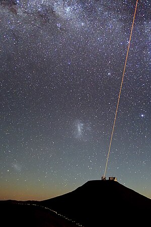
Currently ring lasers are used most frequently as gyroscopes (ring laser gyroscope; (figure 2)) in moving vessels like cars, ships, planes, and missiles. The world's largest ring lasers can detect details of the Earth's rotation. Such large rings are also capable of extending scientific research in many new directions, including the detection of gravitational waves, Fresnel drag, Lense-Thirring effect, and quantum-electrodynamic effects (see Ring Lasers for Research).
In a rotating ring laser gyroscope, the two counter-propagating waves are slightly shifted in frequency and an interference pattern is observed, which is used to determine the rotational speed. The response to a rotation is a frequency difference between the two beams, which is proportional to the rotation rate of the ring laser (Sagnac effect). The difference can easily be measured. Generally however, any non reciprocity in the propagation between the two beams leads to a beat frequency.
Figure 2.Commercial Ring Laser Gyro encased in quartz.
A ring can be constructed with other optically active materials that are able to conduct a beam with low losses. One type of ring laser design is a single crystal design, where light reflects around inside the laser crystal so as to circulate in a ring. This is the "monolithic crystal" design, and such devices are known as "non-planar ring oscillators" (NPROs) or MISERs. There are also ring fiber lasers. Since typically the achievable quality factors are low, such rings cannot be used for research where quality factors above 1012 are sought and are achievable.
Shortly after the discovery of the laser, a seminal paper by Rosenthal appeared in 1962,
which proposed what was later called a ring laser. While the ring laser
shares with regular (linear) lasers features like extreme
monochromaticity and high directivity, it differs in its inclusion of an
area. With the ring laser, one could distinguish two beams in opposite
directions. Rosenthal anticipated that the beam frequencies could be
split by effects that affected the two beams in different ways. Although
some may consider Macek et al. has built the first large ring laser (1
meter × 1 meter).
The US patent office has decided the first ring laser was built under
Sperry scientist, Chao Chen Wang, (see US Patent 3,382,758) based on the
Sperry laboratory records. Wang showed that simply rotating it could
generate a difference in the frequencies of the two beams (Sagnac).
An industry focusing on smaller ring laser gyros emerged, with
decimeter-sized ring lasers. Later it was found that any effect that
affects the two beams in nonreciprocal fashion produces a frequency
difference, as Rosenthal anticipated. Tools to analyze and construct
rings were adapted from regular lasers, including methods to calculate
the signal-to-noise ratio and to analyze beam characteristics. New
phenomena unique to rings appeared, including lock-in, pulling,
astigmatic beams, and special polarizations. Mirrors play a much greater
role in ring lasers than in linear lasers, leading to the development
of particularly high quality mirrors.
The resolution of large ring lasers has dramatically improved, as a result of a 1000-fold improvement in the quality factor (see Table 1). This improvement is largely a result of the removal of interfaces that the beams need to traverse as well as the improvements on technology which allowed a dramatic increase in measurement time (see section on Line Width). A 1 m × 1 m ring built in Christchurch, New Zealand in 1992 was sensitive enough to measure the Earth's rotation (figure 3), and a 4 m × 4 m ring built in Wettzell, Germany improved the precision of this measurement to six digits (figure 4).
Figure 3. The Canterbury ring, built in 1992.
Figure 4. Grossring in Wettzell, Germany, built by Zeiss (Oberkochen, Germany).
Critical variables in the construction of a ring laser include:
1. Size: Larger ring lasers can measure lower frequencies. The sensitivity of large rings increases quadratically with size.
2. Mirrors: High reflectivity is important.
3. Stability: The assembly must be attached to or built within a substance that changes minimally in response to temperature fluctuations (e.g. Zerodur, or bedrock for extremely large rings).
4. Gas: HeNe generates beams with the most desirable features for large ring lasers. For gyros, in principle any material that can be used to generate monochromatic light beams is applicable.
The signal frequency is
S = Δfs = 4 ,
,
where is the area vector,
  is the rotation rate vector, λ is the vacuum wavelength, L is the perimeter. (For complicated geometries like nonplanar rings or figure-8 rings, the definitions
 and L =
  are to be used.)
The noise frequencies are
N = ,
,
where is the one-sided power spectral density of quantum noise, h is Planck’s
constant, f is the laser frequency, P includes all power losses of the
laser beams, and Q is the quality factor of the ring.
is the one-sided power spectral density of quantum noise, h is Planck’s
constant, f is the laser frequency, P includes all power losses of the
laser beams, and Q is the quality factor of the ring.

P should be maximized but kept below the level that generates additional modes. Q can largely be increased by avoiding losses (e.g. improving the quality of the mirrors). T is only limited by the stability of the device. T reduces the line width by the classic T−1/2 for white noise.
For low-Q rings, an empirical relation for 1/f noise has been ascertained, with the one-sided frequency power spectral density given by , with A≃4. It is notoriously difficult to reduce line width in the presence of this noise.
To decrease the line width further, long measurement times are necessary. A measurement time of 243 days reduced the σ to 50 nHz in the Grossring.
 ,
,
where is the peak field of the beam, E is the field distribution, and r is the distance off beam center.
The mirror sizes have to be chosen large enough to ensure that only very small portions of the gaussian tails are to be cut off, such that the calculated Q (below) is maintained.
The phase is spherical with radius of curvature R. It is customary to combine radius of curvature and spot size into a complex curvature
 .
.
The ring design uses a matrix M1 = for a straight section and M2 =
  for a mirror of focus length f. The relation between mirror radius RM and focus length f is for oblique incidence at angle θ, in plane:
 ,
,
for oblique incidence at angle θ, perpendicular to the plane:
 ,
,
resulting in astigmatic beams.
The matrices have
 .
.
A typical design of a rectangular ring has the following form:


(for the equivalent rays where r = distance of equivalent ray from the axis, r’ = the slope against the axis).
Note that in order for the ray to close on itself, the input column matrix has to equal the output column. This round-trip matrix is actually called ABCD matrix in the literature.
The requirement that the ray is to be closed is therefore .
.
semiconductor Ring Laser
Semiconductor ring lasers (SRLs) are miniature ring laser devices with potential applications in optoelectronics, photonics and all-optical circuits. The first SRLs were developed in the 1980s. Recently, they have been of interest as potential random-access memory storage devices for all-optical computers.
Semiconductor ring lasers are literally ring-shaped optical waveguides with a lasing medium. They have the ability to trap light in a ring, and recirculate it continuously as long as they remain powered. The material of choice for SRLs is indium phosphide. SRLs can be square with corner reflectors, or, as is more common with the smaller designs, have a curved, "racetrack" shape. Devices are currently on the order of a 100 micrometres, but further miniaturization should be possible using existing silicon microelectronics technology.
In the summer of 2010 researchers Dr. Muhammad Maqbool and Kyle Main of Ball State University and Dr. Martin Kordesch of Ohio University were able to successfully develop the first Aluminum Nitride SRL on the order of 20 micrometers in diameter. This SRL was constructed by depositing a 4 micrometer thick semi conducting Aluminum-Nitride film doped with Ti+3 ions onto a stretched fiber optic cable of 12 micrometer diameter. This SRL was shown to have considerable gain and a low threshold pump power, making it a highly efficient laser system. The light was confined only to the film and did not reflect off of the outer surface of the optical fiber. Such an arrangement is called a "Whispering Gallery Mode". Maqbool and Main plan to expand their work to include the development of nano scale SRL's on carbon nanotubes.
SRLs may serve as the basis of a new form of optical random access memory. The direction of circulation of light (clockwise or counterclockwise) would indicate the polarity of the bit (0 or 1). Due in part to the bistable and highly non-linear nature of the devices, they can be fed a starting signal from either direction. The directionality is maintained as long as the device remains powered. Other potential applications include "a digital response device that reshapes optical signals that have become distorted, effectively acting as a gate." and a device for resynchronizing optical signals to eliminate timing "jitter".
A European research project formed in 2006 to study potential applications of SRLs. It is known as IOLOS, (Integrated optical logic and memory using ultra-fast micro-ring bistable semiconductor laser), and will receive funding of €1.25 million over three years. Intense Photonics and Siemens are also providing a further €100,000.
Illustration of a Semiconductor Ring Laser (SRL). The laser cavity is a
waveguide with a racetrack geometry (but this can also be another
geometry), which enables it to lase in two counterpropagating
directions: clockwise (CW) and counterclockwise (CCW). The light is
evanescently coupled out of the cavity to a straight output waveguide. Ring laser
F
Currently ring lasers are used most frequently as gyroscopes (ring laser gyroscope; (figure 2)) in moving vessels like cars, ships, planes, and missiles. The world's largest ring lasers can detect details of the Earth's rotation. Such large rings are also capable of extending scientific research in many new directions, including the detection of gravitational waves, Fresnel drag, Lense-Thirring effect, and quantum-electrodynamic effects (see Ring Lasers for Research).
In a rotating ring laser gyroscope, the two counter-propagating waves are slightly shifted in frequency and an interference pattern is observed, which is used to determine the rotational speed. The response to a rotation is a frequency difference between the two beams, which is proportional to the rotation rate of the ring laser (Sagnac effect). The difference can easily be measured. Generally however, any non reciprocity in the propagation between the two beams leads to a beat frequency.
Engineering applications
There is a continuous transition between ring lasers for engineering application and ring lasers for research (see Ring Lasers for Research). Rings for engineering have begun to incorporate a vast variety of materials as well as new technology. Historically, the first extension was the use of fiber optics as wave guides, obviating the use of mirrors. However, even rings using the most advanced fiber working in its optimal wavelength range (e.g. SiO2 at 1.5 μm) have vastly higher losses than square rings with four high-quality mirrors. Therefore, fiber optic rings suffice only in high rotation rate applications. For example, fiber optic rings are now common in automobiles.Figure 2.Commercial Ring Laser Gyro encased in quartz.
A ring can be constructed with other optically active materials that are able to conduct a beam with low losses. One type of ring laser design is a single crystal design, where light reflects around inside the laser crystal so as to circulate in a ring. This is the "monolithic crystal" design, and such devices are known as "non-planar ring oscillators" (NPROs) or MISERs. There are also ring fiber lasers. Since typically the achievable quality factors are low, such rings cannot be used for research where quality factors above 1012 are sought and are achievable.
History
| year | rms linewidth |
measurement time |
source |
|---|---|---|---|
| 1972 | 4.5 Hz | 10 s | Stowell |
| 1993 | 68 mHz | 16 s | Bilger |
| 1994 | 31 mHz | 8 h | Stedman |
| 1996 | 8.6 µHz | 8 d | Bilger |
| 2004 | 50 nHz | 243 d | Schreiber |
The resolution of large ring lasers has dramatically improved, as a result of a 1000-fold improvement in the quality factor (see Table 1). This improvement is largely a result of the removal of interfaces that the beams need to traverse as well as the improvements on technology which allowed a dramatic increase in measurement time (see section on Line Width). A 1 m × 1 m ring built in Christchurch, New Zealand in 1992 was sensitive enough to measure the Earth's rotation (figure 3), and a 4 m × 4 m ring built in Wettzell, Germany improved the precision of this measurement to six digits (figure 4).
Figure 3. The Canterbury ring, built in 1992.
Figure 4. Grossring in Wettzell, Germany, built by Zeiss (Oberkochen, Germany).
Construction
In ring lasers, mirrors are used to focus and redirect the laser beams at the corners. While traveling between mirrors, the beams pass through gas-filled tubes. The beams are generally generated through local excitation of the gas by radio frequencies.Critical variables in the construction of a ring laser include:
1. Size: Larger ring lasers can measure lower frequencies. The sensitivity of large rings increases quadratically with size.
2. Mirrors: High reflectivity is important.
3. Stability: The assembly must be attached to or built within a substance that changes minimally in response to temperature fluctuations (e.g. Zerodur, or bedrock for extremely large rings).
4. Gas: HeNe generates beams with the most desirable features for large ring lasers. For gyros, in principle any material that can be used to generate monochromatic light beams is applicable.
The laser beam: theoretical tools
For a ring as a measuring tool, Signal/Noise ratio and line widths are all-important. The signal of the ring as a rotation detector is used, whereas the all-pervasive white, quantum noise is the fundamental noise of the ring. Rings with a low quality factor generate additional low frequency noise. The standard matrix methods for the beam characteristics — curvature and width — are given, as well as the Jones calculus for polarization.Signal-to-noise ratio
The following equations can be used to calculate the signal-to-noise ratio, S/N for rotation.The signal frequency is
S = Δfs = 4
,where
is the area vector, is the rotation rate vector, λ is the vacuum wavelength, L is the perimeter. (For complicated geometries like nonplanar rings or figure-8 rings, the definitions and L = are to be used.)The noise frequencies are
N =
,where
is the one-sided power spectral density of quantum noise, h is Planck’s
constant, f is the laser frequency, P includes all power losses of the
laser beams, and Q is the quality factor of the ring.Line width
Ring Lasers serve as frequency measuring devices. As such, single Fourier components, or lines in frequency space are of major importance in ring outputs. Their widths are determined by the prevailing noise spectra. The major noise contribution is typically white quantum noise If this noise is the only one present, the rms-line width sigma is obtained by corrupting the signal (represented by a δ function) with this noise in the interval 0-T. The result is:P should be maximized but kept below the level that generates additional modes. Q can largely be increased by avoiding losses (e.g. improving the quality of the mirrors). T is only limited by the stability of the device. T reduces the line width by the classic T−1/2 for white noise.
For low-Q rings, an empirical relation for 1/f noise has been ascertained, with the one-sided frequency power spectral density given by
, with A≃4. It is notoriously difficult to reduce line width in the presence of this noise.To decrease the line width further, long measurement times are necessary. A measurement time of 243 days reduced the σ to 50 nHz in the Grossring.
Beam characteristics
The beam in ring lasers is typically excited by High-Frequency excitation of a laser gas. Although it has been shown that ring lasers can be excited in all kinds of modes, including microwave-related modes, a typical ring laser mode has a Gaussian, closed shape, given proper adjustment of mirror position The analysis of beam properties (curvature radius, width, position of waists, polarization) is done with matrix methods, where the elements of the closed beam circuit, mirrors and distances in between, are given 2 × 2 matrices. The results are distinct for circuits with n mirrors. Typically, there are n waists. For stability, there has to be at least one curved mirror in the circuit. Out-of-plane rings have circular polarization. The choice of mirror radii and mirror separation is not arbitrary.Curvature radius and width
The beam has a spot size w:,where
is the peak field of the beam, E is the field distribution, and r is the distance off beam center.The mirror sizes have to be chosen large enough to ensure that only very small portions of the gaussian tails are to be cut off, such that the calculated Q (below) is maintained.
The phase is spherical with radius of curvature R. It is customary to combine radius of curvature and spot size into a complex curvature
.The ring design uses a matrix M1 =
for a straight section and M2 = for a mirror of focus length f. The relation between mirror radius RM and focus length f is for oblique incidence at angle θ, in plane:,for oblique incidence at angle θ, perpendicular to the plane:
,resulting in astigmatic beams.
The matrices have
.A typical design of a rectangular ring has the following form:
(for the equivalent rays where r = distance of equivalent ray from the axis, r’ = the slope against the axis).
Note that in order for the ray to close on itself, the input column matrix has to equal the output column. This round-trip matrix is actually called ABCD matrix in the literature.
The requirement that the ray is to be closed is therefore
.
Please Visit link
BalasHapushttps://supply.ctdi.com/shop/productdetail/1514970/rbs-xcu