DOT MATRIX THEOREMA

Basically DOT matrix LED display which is arranged so to turn led to the (x, x) takes the combination of voltage between Pin rows and columns .

Markers foot marking number one is writing, the leftmost No. 1 .... rightmost no 7
Crossing to the right on No. 8 to the upper left of the number 14
Some feet are not used so marked bar (negation) is not connected
Crossing to the right on No. 8 to the upper left of the number 14
Some feet are not used so marked bar (negation) is not connected
Then to facilitate the control and pin it is necessary to save the scanning process (typically columns ...) whereas in the corresponding bit line given letters / characters to be displayed corresponding to the scanning position.
Scanning for columns intended to provide a "1" high (for common cathode) or "0" for the common anode, for other columns rated the negation of the column who rated 1 earlier ..... so the next to the next column to the last column of the series led matrix .. and repeatedly from the front again. This process is done very quickly so that our eyes see it remain as a silent character's mouth.
for example, want to display the letters A, is generally described as follows:
0000000
0000000
0000000
0000000
0000000
0000000
0000000
from the image above logic like this:
- When the first column (scan column 1 = 1 / high / 2.4 v) the bits are given on the lines of "1.11 million", so that if met 1 versus 1 no current flows, so the LED die, if one met 0 then a current flows, lED lights up
- So also for the second column, while the second column by the voltage on the bit lines that is given is "1101011"
- And so, when it reaches the end of the column will be repeated to column 1 again
- In order to perform scanning is usually performed by utilizing the shift register, or the simplest to use the IC 4017 which led cascade into a long walk
X . I
Practice LED and battery

let's make an experiment on board the project board : 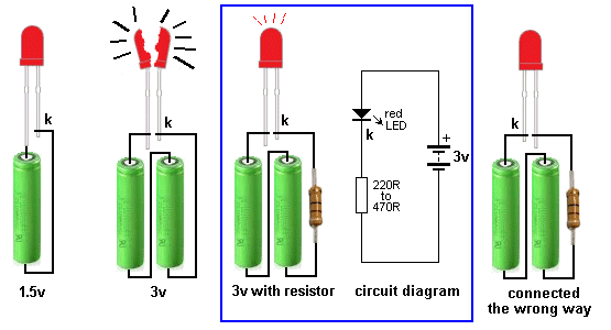
Prepare components include:
- Battery AA 3 Fruit and place the battery (if any).
- 220 ohm resistor.
- Led small
- Battery AA 3 Fruit and place the battery (if any).
- 220 ohm resistor.
- Led small

Connect the battery cables to the upper portion of the breadboard to make the power supply lines.
Now we connect the LED and Resistor corresponding circuit images. Take resistor and plug the hole breadboard where each foot is on a different column. Then proceed to connect the LED, Anode legs usually marked with legs that are longer, plugged into the hole that one column with one foot Resistor. Foot shorter cathode which is plugged into a hole with a different column
Also create a jumper cable that will connect the holes breadboard that will be connected to the other hole. Jumper cables made of a single cable that ends pared approximately 50mm.

Subsequently connect the resistor and LED foot (feet unconnected) toward the power supply by using a jumper cable. Resistor heading to the positive pole (+) and the cathode of the LED to the pole to the negative (-).

Results of the circuit in the breadboard is the LED will light
X . II
Practice: 2 LED FLIP FLOP With IC 555
Prepare ingredients / components as follows:
1. Timer IC 555
2. 10K ohm resistor (1buah), 100K ohm (1 Piece) and 220 ohm (2 pieces)
3. 50K ohm potentiometer
4. Capacitors 10uF (1 piece)
5. LED 2buah
6. Buzzer 5V
7. Battery 4.5V
8. Jumper Cables
Circuit schematic as follows:


Step assemble to breadboard:
1. Create a Power line above to below to the positive and negative poles of the battery connect with the corresponding.
2. Place the IC 555 with a sideways direction (horizontal), with the first leg (marked with dots) is under the center divider breadboard. Connect the leg and foot 8 to + 1 to - by using a jumper cable.
 3. Connect with foot jumper 8 to the foot 4, and a second leg to the foot 6
4. Take a 10K ohm resistor and connect it between the legs 7 and 8 IC 555. Find an empty hole and is located straight to the IC. Likewise with R 100k Ohm connect between 2 feet and 7 feet, and connect 10uF capacitor with a second leg (pole +) and the first leg (pole -).

5. Take the LED and 220 ohm resistor each 2 pieces. Connect foot hole 3 with a jumper to do a bit away from the IC and then stacking as schematic. The first resistor jumper from the tip toward the hole in an empty field, then in the hole in the same column of Led plugged Anode Cathode led No. 1. No. 1 is connected to a pole (-) of the power line. While the second resistor is plugged into the power line (+) and the other end towards the hole in the middle of an empty field. Furthermore anode led the 2nd plugged in one column with last resistor and cathode of LED No. 2 towards the end of a jumper cable.

6. Connect the battery in the power line and Led will flash alternately. To vary the speed of blinking can change the value of capacitor or component values of resistors (R1). But in general, and most likely is to replace the R1 component of the Variable Resistor or Potentio meter resistance value which can be changed. There are several types of variable resistor as shown below:

In general, the variable resistors have 3 pieces leg, where to get the resistance in the circuit that we want simply by connecting the middle leg and one leg side. Move it around the button by hand or using a screwdriver to get that desired resistance value. By using a variable resistor create blinking speed of the circuit can be arranged Flip-Flop.

7. IC 555 can also be used to generate simple using the siren buzzer components. Connect the output feet (3 feet) with a pole (+) of the buzzer and the pole (-) of the buzzer connected to the pole (-) of the power line. The result is the sound of a siren out of the buzzer.
X . III
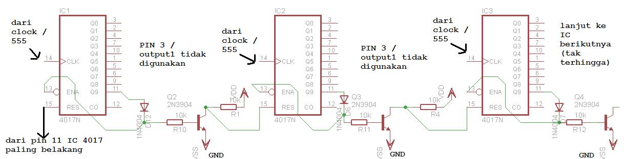
Practice: LED RUNNING with IC 4017
Ingredients :
1. IC 555
2. IC 4017
3. 10k ohm resistor (1buah), 100Kohm (1 piece) or replaced by a potentio meter 100k ohms, 220 ohms (10 pieces)
4. Capacitors 10 uF (1 piece)
5. 10 LEDs
6. Battery 4.5V
7. Jumper Cables taste
schematic:

Description: IC foot note that no sequence, adjust the number of legs on the schematic with actual IC pins in the legs
Assemble step to Breadboard:
1. Once familiar stringing the 555 experiment this experiment would have been easy just follow the schematic drawing shown earlier, and results in the breadboard like this:

Note to IC 4017 is connected to power line feet 8 pole (-) while connected to a 16 foot pole (+)2. Turn-turn potentio meter to change the velocity of shear from the LED.3. Animation of the LEDs can be arranged in such a way so as to form
the desired movement as an example by putting 1-10-2-9-3-8-4-7-5-6 LED
arrangement would be associated with the effect of "cyclops" or back and
forth.4. IC 555 and 4017 can be fed up to 12V, so as to turn the LEDs are mounted series of 5 pieces. Try to be creative by adding LEDs in each output leg and try to combine it with a combination of LED colors.5. If using more LEDs, it can use a common transistor like BD139 or MJ31, as in the picture. Set the input voltage to the LED illuminate. Basically if LEDs in series, the input voltage required to follow the formulaVin = V forward * n led = diode forward voltage multiplied by the number of LEDs In general, the LED has a forward V 2.4 V, so if using five LEDs takes approximately 12 Volt. If
using more than 5 LED (such as 20 LEDs) then the LED in series 5 pieces
and then in parallel with three other series circuit. Because the flow of 4017 is quite small, it is necessary transistors for greater current flow.

tegangan sesuai rumus = appropriate voltages formula
dari output 4017 = from output 4017
X . IIII
DICE + 7 SEGMENT DISPLAY DIGITAL with IC 4026
Prepare Materials as follows:
1. IC 555
2. IC 4026
3. 10k ohm resistor (1buah), 100Kohm (1 piece) or replaced by a potentio meter 100k ohms, 220 ohms (7 pieces if necessary)
4. Capacitors 10 uF (1 piece)
5. Push button / push button
6. 7 Segment COMMON cathode (not the one buying !!)
7. Battery 4.5V
8. Jumper Cables taste
schematic :

Click for more details
*) Note: notice that no sequence IC feet, adjust the number foot on the schematic with actual IC pins in the legs
*) Note: notice that no sequence IC feet, adjust the number foot on the schematic with actual IC pins in the legs
Assemble step to Breadboard:
1. Once familiar stringing the 555 experiment this experiment would have been easy just follow the schematic drawing shown earlier, and results in the breadboard like this:

2. push button has four feet where there are 2 pairs of legs which are connected.
3. If the battery voltage exceeds 6V, then before going into 7 segments necessary ohm resistor 220 or more. If using 4.5 V resistor can not be used.
4. Rotate-turn potentio meter to obtain the desired rate of addition of digits.
5. If the digit changes speed very quickly, then this circuit can be used as a "ELECTRONIC DICE". So when the button is pressed, the numbers will stop the digit we do not expect before.
"Dice the numbers 1 to 6 ...?

.we make logic that would eliminate the number "0" and it will reset the system when the counter has exceeded 6. Schematic her as follows:

Schematic above utilizing DEI pin (enable input display) that will enable the seven segments when getting V + and while getting a logic 0 / ground, then the 7 segment will die. Transistor 2N3904 (NPN) is used as an inverter logic output 0 from the counter 4017.
To reset when the counter reaches 6 then utilized output 7 of 4017 which will reset all system when output 7 is enabled.
To reset when the counter reaches 6 then utilized output 7 of 4017 which will reset all system when output 7 is enabled.

X . IIIII
Dot matrix
An alternate form of information display using lines and curves is known as a vector display, was used with early computing devices such as air traffic control radar displays and pen-based plotters but is no longer used. Electronic vector displays were typically monochrome only, and either don't fill in the interiors of closed vector shapes, or shape-filling is slow, time-consuming, and often non-uniform, as on pen-based plotters.
In printers, the dots are usually the darkened areas of the paper. In displays, the dots may light up, as in an LED, CRT, or plasma display, or darken, as in an LCD.

Dot matrix pattern woven into fabric in 1858, using punched cards on a Jacquard loom.

Close-up view of dot matrix text produced by an impact printer.
Usage in printers
As an impact printer, the term mainly refers to low-resolution impact printers, with a column of 8, 9 or 24 "pins" hitting an ink-impregnated fabric ribbon, like a typewriter ribbon, onto the paper. It was originally contrasted with both daisy wheel printers and line printers that used fixed-shape embossed metal or plastic stamps to mark paper.However, almost all modern computer printers also create their output as matrices of dots, but use a different technology like laser printing or inkjet printing, and are not called dot matrix printers. Impact printers survive where multi-part forms are needed, as the pins can impress dots through multiple layers of paper to make a carbonless copy, for security purposes.
All types of electronic printers typically generate image data as a two-step process. First the information to be printed is converted into a dot matrix using a raster image processor, and the output is a dot matrix referred to as a raster image, which is a complete full-page rendering of the information to be printed. Raster image processing may occur in either the printer itself using a page description language such as Adobe Postscript, or may be performed by printer driver software installed on the user's computer.
Early 1980s impact printers used a simple form of internal raster image processing, using low-resolution built-in bitmap fonts to render raw character data sent from the computer, and only capable of storing enough dot matrix data for one printed line at a time. External raster image processing was possible such as to print a graphical image, but was commonly extremely slow and data was sent one line at a time to the impact printer.
Depending on the printer technology the dot size or grid shape may not be uniform. Some printers are capable of producing smaller dots and will intermesh the small dots within the corners larger ones for antialiasing. Some printers have a fixed resolution across the printhead but with much smaller micro-stepping for the mechanical paper feed, resulting in non-uniform dot-overlapping printing resolutions like 600×1200 dpi.
A dot matrix is useful for marking materials other than paper. In manufacturing industry, many product marking applications use dot matrix inkjet or impact methods. This can also be used to print 2D matrix codes, e.g. Datamatrix.
Usage in computers
Although the output of modern computers is generally all in the form of dot matrices (technically speaking), computers may internally store data as either a dot matrix or as a vector pattern of lines and curves. Vector data encoding requires less memory and less data storage, in situations where the shapes may need to be resized, as with font typefaces. For maximum image quality using only dot matrix fonts, it would be necessary to store a separate dot matrix pattern for the many different potential point sizes that might be used. Instead, a single group of vector shapes is used to render all the specific dot matrix patterns needed for the current display or printing task.LED matrix

A LED matrix display scanning by rows to make the letter W
The primary difference between a common LED matrix and an OLED display is the large, low resolution dots. The OLED monitor functionally works the same, except there are many times more dots, and they are all much smaller, allowing for greater detail in the displayed patterns.
X . IIIIII
Dot-matrix display
A dot-matrix display is a display device used to display information on machines, clocks, railway departure indicators and many other devices requiring a simple display device of limited resolution.The display consists of a dot matrix of lights or mechanical indicators arranged in a rectangular configuration (other shapes are also possible, although not common) such that by switching on or off selected lights, text or graphics can be displayed. A dot matrix controller converts instructions from a processor into signals which turns on or off lights in the matrix so that the required display is produced.
Pixel resolutions

"A Matrix Display in the size 20x2" – This is a classic 5x7 dot matrix LCD used in some early cellphones and vending machines
- 128×16 (Two lined)
- 128×32 (Four lined)
- 128×64 (Eight lined)
- 92×31 (Four or three lined)
Character resolutions
- A common size for a character is 5×7 pixels, either separated with blank lines with no dots (in most text-only displays), or with lines of blank pixels (making the real size 6x8). This is seen on most graphic calculators, such as Casio calculators or TI-82 and superior.
- A smaller size is 3×5 (or 4x6 when separated with blank pixels). This is seen on the TI-80 calculator as a "pure", fixed-size 3×5 font, or on most 7×5 calculators as a proportional (1×5 to 5×5) font. The disadvantage of the 7×5 matrix and smaller is that lower case characters with descenders are not practical. A matrix of 11×9 is often used to give far superior resolution.
- Dot matrix displays of sufficient resolution can be programmed to emulate the customary seven-segment numeral patterns.
- A larger size is 5×9 pixels, which is used on many Natural Display calculators.

X . IIIIIII
Digital Light Processing
"DLP projector" redirects here. For other projection devices, see Movie projector.
The DLP Logo

The Christie Mirage 5000, a 2001 DLP projector.
DLP technology is used in DLP front projectors (standalone projection units for classrooms and business primarily), DLP rear projection television sets, and digital signs. It is also used in about 85% of digital cinema projection, and in additive manufacturing as a power source in some printers to cure resins into solid 3D objects.
Smaller "pico" chipsets are used in mobile devices including cell phone accessories and projection display functions embedded directly into phones.
Digital micromirror device

Diagram of a Digital micromirror showing the mirror mounted on the
suspended yoke with the torsion spring running bottom left to top right
(light grey), with the electrostatic pads of the memory cells below (top
left and bottom right)
Rapidly toggling the mirror between these two orientations (essentially on and off) produces grayscales, controlled by the ratio of on-time to off-time.
Color in DLP projection
There are two primary methods by which DLP projection systems create a color image: those used by single-chip DLP projectors, and those used by three-chip projectors. A third method, sequential illumination by three colored light emitting diodes, is being developed, and is currently used in televisions manufactured by Samsung.Single-chip projectors
 |
 |
 |
 |
 |
|||
| Interior view of a single-chip DLP projector, showing the light path. Light from the lamp enters a reverse-fisheye, passes through the spinning color wheel, crosses underneath the main lens, reflects off a front-surfaced mirror, and is spread onto the DMD (red arrows). From there, light either enters the lens (yellow) or is reflected off the top cover down into a light-sink (blue arrows) to absorb unneeded light. Top row shows overall components, closeups of 4-segment RGBW color wheel, and light-sink diffuser/reflection plate on top cover. | |||
The DLP chip is synchronized with the rotating motion of the color wheel so that the green component is displayed on the DMD when the green section of the color wheel is in front of the lamp. The same is true for the red, blue and other sections. The colors are thus displayed sequentially at a sufficiently high rate that the observer sees a composite "full color" image. In early models, this was one rotation per frame. Now, most systems operate at up to 10x the frame rate.
The black level of a single-chip DLP depends on how unused light is being disposed. If the unused light is scattered to reflect and dissipate on the rough interior walls of the DMD / lens chamber, this scattered light will be visible as a dim gray on the projection screen, when the image is fully dark. Deeper blacks and higher contrast ratios are possible by directing unused HID light away from the DMD / lens chamber into a separate area for dissipation, and shielding the light path from unwanted internal secondary reflections.
The color wheel "rainbow effect"
DLP projectors utilizing a mechanical spinning color wheel may exhibit an anomaly known as the "rainbow effect". This is best described as brief flashes of perceived red, blue, and green "shadows" observed most often when the projected content features high contrast areas of moving bright or white objects on a mostly dark or black background. Common examples are the scrolling end credits of many movies, and also animations with moving objects surrounded by a thick black outline. Brief visible separation of the colours can also be apparent when the viewer moves their eyes quickly across the projected image. Some people perceive these rainbow artifacts frequently, while others may never see them at all.This effect is caused by the way the eye follows a moving object on the projection. When an object on the screen moves, the eye follows the object with a constant motion, but the projector displays each alternating color of the frame at the same location for the duration of the whole frame. So, while the eye is moving, it sees a frame of a specific color (red, for example). Then, when the next color is displayed (green, for example), although it gets displayed at the same location overlapping the previous color, the eye has moved toward the object's next frame target. Thus, the eye sees that specific frame color slightly shifted. Then, the third color gets displayed (blue, for example), and the eye sees that frame's color slightly shifted again. This effect is not perceived only for the moving object, but the whole picture. Additionally, multi-color LED-based and laser-based single-chip projectors are able to eliminate the spinning wheel and minimize the rainbow effect, since the pulse rate of LEDs and laser are not limited by physical motion. "Three-chip DLP projectors have no color wheels, and thus do not manifest this [rainbow] artifact."
Three-chip projectors
A three-chip DLP projector uses a prism to split light from the lamp, and each primary color of light is then routed to its own DLP chip, then recombined and routed out through the lens. Three chip systems are found in higher-end home theater projectors, large venue projectors and DLP Cinema projection systems found in digital movie theaters.According to DLP.com, the three-chip projectors used in movie theaters can produce 35 trillion colors. The human eye is suggested to be able to detect around 16 million colors, which is theoretically possible with the single chip solution. However, this high color precision does not mean that three-chip DLP projectors are capable of displaying the entire gamut of colors we can distinguish (this is fundamentally impossible with any system composing colors by adding three constant base colors). In contrast, it is the one-chip DLP projectors that have the advantage of allowing any number of primary colors in a sufficiently fast color filter wheel, and so the possibility of improved color gamuts is available.
Light source

The InFocus IN34, a DLP projector
Xenon arc lamps
For xenon arc lamps, during start-up, the lamp is ignited by a 5–20-kilovolt pulse from a current-regulating ballast to initiate an arc between two electrodes in the quartz tube. After warmup, the ballast's output voltage drops to approximately 60 volts while keeping the relative current high. As the lamp ages, the arc tube's electrodes wear out and light output declines somewhat, while waste heating of the lamp increases. The lamp's end of life is typically indicated by an LED on the unit or an onscreen text warning, necessitating replacement of the lamp unit.When a lamp is operated past its rated lifespan, the efficiency declines significantly, the lightcast may become uneven, and the lamp starts to operate extremely hot, to the point that the power wires can melt off the lamp terminals. Eventually, the required startup voltage will also rise to the point where ignition can no longer occur. Secondary protections such as a temperature monitor may shut down the projector, but a thermally overstressed quartz arc tube can also crack and/or explode. However, practically all lamp housings contain heat-resistant barriers (in addition to those on the lamp unit itself) to prevent the red-hot quartz fragments from leaving the area.
LED-based DLPs
The first commercially available LED-based DLP HDTV was the Samsung HL-S5679W in 2006, which also eliminated the use of a color wheel. Besides long lifetime eliminating the need for lamp replacement and elimination of the color wheel, other advantages of LED illumination include instant-on operation and improved color, with increased color saturation and improved color gamut to over 140% of the NTSC color gamut. Samsung expanded the LED model line-up in 2007 with products available in 50-, 56- and 61-inch screen sizes. In 2008, the third generation of Samsung LED DLP products were available in 61" (HL61A750) and 67" (HL67A750) screen sizes.Ordinary LED technology does not produce the intensity and high-lumen output characteristics required to replace arc lamps. The special patented LEDs used in all of the Samsung DLP TVs are PhlatLight LEDs, designed and manufactured by US-based Luminus Devices. A single RGB PhlatLight LED chipset illuminates these projection TVs. The PhlatLight LEDs are also used in a new class of ultra-compact DLP front projector commonly referred to as a "pocket projector" and have been introduced in new models from LG Electronics (HS101), Samsung electronics (SP-P400) and Casio (XJ-A series). Home Theater projectors will be the next category of DLP projectors that will use PhlatLight LED technology. At InfoComm, June 2008 Luminus and TI announced their collaboration on using their technology on home theater and business projectors and demonstrated a prototype PhlatLight LED-based DLP home theater front projector. They also announced products will be available in the marketplace later in 2008 from Optoma and other companies to be named later in the year.
Luminus Devices PhlatLight LEDs have also been used by Christie Digital in their DLP-based MicroTiles display system. It is a modular system built from small (20 inch diagonal) rear projection cubes, which can be stacked and tiled together to form large display canvasses with very small seams. The scale and shape of the display can have any size, only constrained by practical limits.
Laser-based DLPs
The first commercially available laser-based DLP HDTV was the Mitsubishi L65-A90 LaserVue in 2008, which also eliminated the use of a color wheel. Three separate color lasers illuminate the digital micromirror device (DMD) in these projection TVs, producing a richer, more vibrant color palette than other methods. See the laser video display article for more information.Digital cinema
Main article: Digital cinema

DLP CINEMA. A Texas Instruments Technology

Texas Instruments, DLP Cinema Prototype Projector, Mark V, 2000

The NEC Cinema DLP projector in 2006
DLP Cinema does not manufacture the end projectors, but rather provides the projection technology and works closely with Barco, Christie Digital and NEC who make the end projection units. DLP Cinema is available to theatre owners in multiple resolutions depending on the needs of the exhibitor. These include, 2K – for most theatre screens, 4K - for large theatre screens, and S2K, which was specifically designed for small theatres, particularly in emerging markets worldwide.
On February 2, 2000, Philippe Binant, technical manager of Digital Cinema Project at Gaumont in France, realized the first digital cinema projection in Europe with the DLP CINEMA technology developed by Texas Instruments. DLP is the current market-share leader in professional digital movie projection, largely because of its high contrast ratio and available resolution as compared to other digital front-projection technologies. As of December 2008, there are over 6,000 DLP-based Digital Cinema Systems installed worldwide.
DLP projectors are also used in RealD Cinema and newer IMAX theatres for 3-D films.
Manufacturers and marketplace
|
|
|
|

56 inch DLP rear-projection TV
Pros
- Smooth (at 1080p resolution), jitter-free images
- Perfect geometry and excellent grayscale linearity achievable
- Usually excellent ANSI contrast
- The use of a replaceable light source means a potentially longer life than CRTs and plasma displays (this may also be a con as listed below)
- The light source is more-easily replaceable than the backlights used with LCDs, and on DLPs is often user-replaceable.
- The light from the projected image is not inherently polarized.
- New LED and laser DLP display systems more or less eliminate the need for lamp replacement.
- DLP offers affordable 3D projection display from a single unit and can be used with both active and passive 3D solutions.
- Lighter weight than LCD and plasma televisions
- Unlike their LCD and plasma counterparts, DLP screens do not rely on fluids as their projection medium and are therefore not limited in size by their inherent mirror mechanisms, making them ideal for increasingly larger high-definition theater and venue screens.
- DLP projectors can process up to 7 separate colors, giving them a wider color gamut.
Cons

The rear panel of a Mitsubishi XD300U shows the output and input jacks which are available.
- Some viewers are bothered by the "rainbow effect" present in colour-wheel models - particularly in older models (explained above).
- Rear projection DLP TVs are not as thin as LCD or plasma flat-panel displays (although approximately comparable in weight), although some models as of 2008 are becoming wall-mountable (while still being 10" to 14" thick)
- Replacement of the lamp / light bulb in lamp-based units. The life span of a mercury lamp averages 2000–5000 hours and the replacement cost for these range from $99 – 350, depending on the brand and model. Newer generations' units use LEDs or lasers which effectively eliminate this issue, although replacement LED chips could potentially be required over the extended lifespan of the television set.
- Some viewers find the high pitch whine of the color wheel to be an annoyance. However, the drive system can be engineered to be silent and some projectors don't produce any audible color wheel noise.
- Dithering noise may be noticeable, especially in dark image areas. Newer (post ~2004) chip generations have less noise than older ones.
- Error-diffusion artifacts caused by averaging a shade over different pixels, since one pixel cannot render the shade exactly
- Response time in video games may be affected by upscaling lag. While all HDTVs have some lag when upscaling lower resolution input to their native resolution, DLPs are commonly reported to have longer delays. Newer consoles such as the Xbox 360 do not have this problem as long as they are connected with HD-capable cables.
- Reduced viewing angle as compared to direct-view technologies such as CRT, plasma, and LCD
- May use more electricity, and generate more heat, than competing technologies.
- Some people may be able to observe a phenomenon in which the projected contents appear to be cycling through its colours for the duration of the presentation. This is most easily seen by using a camera's 'live view' mode on projected content.
DLP, LCD, and LCoS rear projection
The most similar competing system to DLP is known as LCoS (liquid crystal on silicon), which creates images using a stationary mirror mounted on the surface of a chip, and uses a liquid crystal matrix (similar to a liquid crystal display) to control how much light is reflected. DLP-based television systems are also arguably considered to be smaller in depth than traditional projection television.X . IIIIIIII
OLED Organic light-emitting diode
There are two main families of OLED: those based on small molecules and those employing polymers. Adding mobile ions to an OLED creates a light-emitting electrochemical cell (LEC) which has a slightly different mode of operation. OLED displays can use either passive-matrix (PMOLED) or active-matrix (AMOLED) addressing schemes. Passive matrix OLEDs (PMOLED) uses a simple control scheme in which you control each row (or line) in the display sequentially whereas active-matrix OLEDs (AMOLED) require a thin-film transistor backplane to switch each individual pixel on or off, but allow for higher resolution and larger display sizes.
An OLED display works without a backlight; thus, it can display deep black levels and can be thinner and lighter than a liquid crystal display (LCD). In low ambient light conditions (such as a dark room), an OLED screen can achieve a higher contrast ratio than an LCD, regardless of whether the LCD uses cold cathode fluorescent lamps or an LED backlight.

Prototype OLED lighting panels

History
André Bernanose and co-workers at the Nancy-Université in France made the first observations of electroluminescence in organic materials in the early 1950s. They applied high alternating voltages in air to materials such as acridine orange, either deposited on or dissolved in cellulose or cellophane thin films. The proposed mechanism was either direct excitation of the dye molecules or excitation of electrons.In 1960 Martin Pope and some of his co-workers at New York University developed ohmic dark-injecting electrode contacts to organic crystals. They further described the necessary energetic requirements (work functions) for hole and electron injecting electrode contacts. These contacts are the basis of charge injection in all modern OLED devices. Pope's group also first observed direct current (DC) electroluminescence under vacuum on a single pure crystal of anthracene and on anthracene crystals doped with tetracene in 1963 using a small area silver electrode at 400 volts. The proposed mechanism was field-accelerated electron excitation of molecular fluorescence.
Pope's group reported in 1965 that in the absence of an external electric field, the electroluminescence in anthracene crystals is caused by the recombination of a thermalized electron and hole, and that the conducting level of anthracene is higher in energy than the exciton energy level. Also in 1965, W. Helfrich and W. G. Schneider of the National Research Council in Canada produced double injection recombination electroluminescence for the first time in an anthracene single crystal using hole and electron injecting electrodes, the forerunner of modern double-injection devices. In the same year, Dow Chemical researchers patented a method of preparing electroluminescent cells using high-voltage (500–1500 V) AC-driven (100–3000 Hz) electrically insulated one millimetre thin layers of a melted phosphor consisting of ground anthracene powder, tetracene, and graphite powder.Their proposed mechanism involved electronic excitation at the contacts between the graphite particles and the anthracene molecules.
Roger Partridge made the first observation of electroluminescence from polymer films at the National Physical Laboratory in the United Kingdom. The device consisted of a film of poly(N-vinylcarbazole) up to 2.2 micrometers thick located between two charge injecting electrodes. The results of the project were patented in 1975 and published in 1983.
The first practical OLEDs
Hong Kong-born American physical chemist Ching W. Tang and his co-worker Steven Van Slyke at Eastman Kodak built the first practical OLED device in 1987. This was a revolution for the technology. This device used a novel two-layer structure with separate hole transporting and electron transporting layers such that recombination and light emission occurred in the middle of the organic layer; this resulted in a reduction in operating voltage and improvements in efficiency.Research into polymer electroluminescence culminated in 1990 with J. H. Burroughes et al. at the Cavendish Laboratory in Cambridge reporting a high efficiency green light-emitting polymer based device using 100 nm thick films of poly(p-phenylene vinylene).
Universal Display Corporation holds the majority of patents concerning the commercialization of OLEDs.
Working principle

Schematic of a bilayer OLED: 1. Cathode (−), 2. Emissive Layer, 3. Emission of radiation, 4. Conductive Layer, 5. Anode (+)
Originally, the most basic polymer OLEDs consisted of a single organic layer. One example was the first light-emitting device synthesised by J. H. Burroughes et al., which involved a single layer of poly(p-phenylene vinylene). However multilayer OLEDs can be fabricated with two or more layers in order to improve device efficiency. As well as conductive properties, different materials may be chosen to aid charge injection at electrodes by providing a more gradual electronic profile, or block a charge from reaching the opposite electrode and being wasted. Many modern OLEDs incorporate a simple bilayer structure, consisting of a conductive layer and an emissive layer. More recent developments in OLED architecture improves quantum efficiency (up to 19%) by using a graded heterojunction. In the graded heterojunction architecture, the composition of hole and electron-transport materials varies continuously within the emissive layer with a dopant emitter. The graded heterojunction architecture combines the benefits of both conventional architectures by improving charge injection while simultaneously balancing charge transport within the emissive region.
During operation, a voltage is applied across the OLED such that the anode is positive with respect to the cathode. Anodes are picked based upon the quality of their optical transparency, electrical conductivity, and chemical stability. A current of electrons flows through the device from cathode to anode, as electrons are injected into the LUMO of the organic layer at the cathode and withdrawn from the HOMO at the anode. This latter process may also be described as the injection of electron holes into the HOMO. Electrostatic forces bring the electrons and the holes towards each other and they recombine forming an exciton, a bound state of the electron and hole. This happens closer to the emissive layer, because in organic semiconductors holes are generally more mobile than electrons. The decay of this excited state results in a relaxation of the energy levels of the electron, accompanied by emission of radiation whose frequency is in the visible region. The frequency of this radiation depends on the band gap of the material, in this case the difference in energy between the HOMO and LUMO.
As electrons and holes are fermions with half integer spin, an exciton may either be in a singlet state or a triplet state depending on how the spins of the electron and hole have been combined. Statistically three triplet excitons will be formed for each singlet exciton. Decay from triplet states (phosphorescence) is spin forbidden, increasing the timescale of the transition and limiting the internal efficiency of fluorescent devices. Phosphorescent organic light-emitting diodes make use of spin–orbit interactions to facilitate intersystem crossing between singlet and triplet states, thus obtaining emission from both singlet and triplet states and improving the internal efficiency.
Indium tin oxide (ITO) is commonly used as the anode material. It is transparent to visible light and has a high work function which promotes injection of holes into the HOMO level of the organic layer. A typical conductive layer may consist of PEDOT:PSS as the HOMO level of this material generally lies between the workfunction of ITO and the HOMO of other commonly used polymers, reducing the energy barriers for hole injection. Metals such as barium and calcium are often used for the cathode as they have low work functions which promote injection of electrons into the LUMO of the organic layer. Such metals are reactive, so they require a capping layer of aluminium to avoid degradation.
Experimental research has proven that the properties of the anode, specifically the anode/hole transport layer (HTL) interface topography plays a major role in the efficiency, performance, and lifetime of organic light emitting diodes. Imperfections in the surface of the anode decrease anode-organic film interface adhesion, increase electrical resistance, and allow for more frequent formation of non-emissive dark spots in the OLED material adversely affecting lifetime. Mechanisms to decrease anode roughness for ITO/glass substrates include the use of thin films and self-assembled monolayers. Also, alternative substrates and anode materials are being considered to increase OLED performance and lifetime. Possible examples include single crystal sapphire substrates treated with gold (Au) film anodes yielding lower work functions, operating voltages, electrical resistance values, and increasing lifetime of OLEDs.
Single carrier devices are typically used to study the kinetics and charge transport mechanisms of an organic material and can be useful when trying to study energy transfer processes. As current through the device is composed of only one type of charge carrier, either electrons or holes, recombination does not occur and no light is emitted. For example, electron only devices can be obtained by replacing ITO with a lower work function metal which increases the energy barrier of hole injection. Similarly, hole only devices can be made by using a cathode made solely of aluminium, resulting in an energy barrier too large for efficient electron injection
Material technologies
Small molecules

Alq3, commonly used in small molecule OLEDs
Molecules commonly used in OLEDs include organometallic chelates (for example Alq3, used in the organic light-emitting device reported by Tang et al.), fluorescent and phosphorescent dyes and conjugated dendrimers. A number of materials are used for their charge transport properties, for example triphenylamine and derivatives are commonly used as materials for hole transport layers. Fluorescent dyes can be chosen to obtain light emission at different wavelengths, and compounds such as perylene, rubrene and quinacridone derivatives are often used. Alq3 has been used as a green emitter, electron transport material and as a host for yellow and red emitting dyes.
The production of small molecule devices and displays usually involves thermal evaporation in a vacuum. This makes the production process more expensive and of limited use for large-area devices, than other processing techniques. However, contrary to polymer-based devices, the vacuum deposition process enables the formation of well controlled, homogeneous films, and the construction of very complex multi-layer structures. This high flexibility in layer design, enabling distinct charge transport and charge blocking layers to be formed, is the main reason for the high efficiencies of the small molecule OLEDs.
Coherent emission from a laser dye-doped tandem SM-OLED device, excited in the pulsed regime, has been demonstrated. The emission is nearly diffraction limited with a spectral width similar to that of broadband dye lasers.
Researchers report luminescence from a single polymer molecule, representing the smallest possible organic light-emitting diode (OLED) device. Scientists will be able to optimize substances to produce more powerful light emissions. Finally, this work is a first step towards making molecule-sized components that combine electronic and optical properties. Similar components could form the basis of a molecular computer.
Polymer light-emitting diodes

poly(p-phenylene vinylene), used in the first PLED
Vacuum deposition is not a suitable method for forming thin films of polymers. However, polymers can be processed in solution, and spin coating is a common method of depositing thin polymer films. This method is more suited to forming large-area films than thermal evaporation. No vacuum is required, and the emissive materials can also be applied on the substrate by a technique derived from commercial inkjet printing. However, as the application of subsequent layers tends to dissolve those already present, formation of multilayer structures is difficult with these methods. The metal cathode may still need to be deposited by thermal evaporation in vacuum. An alternative method to vacuum deposition is to deposit a Langmuir-Blodgett film.
Typical polymers used in pleaded displays include derivatives of poly(p-phenylene vinylene) and polyfluorene. Substitution of side chains onto the polymer backbone may determine the colour of emitted light or the stability and solubility of the polymer for performance and ease of processing.
While unsubstituted poly(p-phenylene vinylene) (PPV) is typically insoluble, a number of PPVs and related poly(naphthalene vinylene)s (PNVs) that are soluble in organic solvents or water have been prepared via ring opening metathesis polymerization. These water-soluble polymers or conjugated poly electrolytes (CPEs) also can be used as hole injection layers alone or in combination with nanoparticles like graphene.
Phosphorescent materials

Ir(mppy)3, a phosphorescent dopant which emits green light.
Main article: Phosphorescent organic light-emitting diode
Phosphorescent organic light emitting diodes use the principle of
electrophosphorescence to convert electrical energy in an OLED into
light in a highly efficient manner, with the internal quantum efficiencies of such devices approaching 100%.Typically, a polymer such as poly(N-vinylcarbazole) is used as a host material to which an organometallic complex is added as a dopant. Iridium complexes such as Ir(mppy)3 are currently the focus of research, although complexes based on other heavy metals such as platinum have also been used.
The heavy metal atom at the centre of these complexes exhibits strong spin-orbit coupling, facilitating intersystem crossing between singlet and triplet states. By using these phosphorescent materials, both singlet and triplet excitons will be able to decay radiatively, hence improving the internal quantum efficiency of the device compared to a standard pleaded where only the singlet states will contribute to emission of light.
Applications of OLEDs in solid state lighting require the achievement of high brightness with good CIE coordinates (for white emission). The use of macromolecular species like polyhedral oligomeric silsesquioxanes (POSS) in conjunction with the use of phosphorescent species such as Ir for printed OLEDs have exhibited brightnesses as high as 10,000 cd/m2.
Tidak ada komentar:
Posting Komentar