Frequency counter
A frequency counter is an electronic instrument, or component of one, that is used for measuring frequency. Frequency counters usually measure the number of oscillations or pulses per second in a periodic electronic signal. Such an instrument is sometimes referred to as a cymometer, particularly one of Chinese manufacture .

Operating principle
Most frequency counters work by using a counter which accumulates the number of events occurring within a specific period of time. After a preset period known as the gate time (1 second, for example), the value in the counter is transferred to a display and the counter is reset to zero. If the event being measured repeats itself with sufficient stability and the frequency is considerably lower than that of the clock oscillator being used, the resolution of the measurement can be greatly improved by measuring the time required for an entire number of cycles, rather than counting the number of entire cycles observed for a pre-set duration (often referred to as the reciprocal technique). The internal oscillator which provides the time signals is called the timebase, and must be calibrated very accurately.If the event to be counted is already in electronic form, simple interfacing to the instrument is all that is required. More complex signals may need some conditioning to make them suitable for counting. Most general purpose frequency counters will include some form of amplifier, filtering and shaping circuitry at the input. DSP technology, sensitivity control and hysteresis are other techniques to improve performance. Other types of periodic events that are not inherently electronic in nature will need to be converted using some form of transducer. For example, a mechanical event could be arranged to interrupt a light beam, and the counter made to count the resulting pulses.
Frequency counters designed for radio frequencies (RF) are also common and operate on the same principles as lower frequency counters. Often, they have more range before they overflow. For very high (microwave) frequencies, many designs use a high-speed prescaler to bring the signal frequency down to a point where normal digital circuitry can operate. The displays on such instruments take this into account so they still display the correct value. Microwave frequency counters can currently measure frequencies up to almost 56 GHz. Above these frequencies the signal to be measured is combined in a mixer with the signal from a local oscillator, producing a signal at the difference frequency, which is low enough to be measured directly.
Accuracy and resolution
The accuracy of a frequency counter is strongly dependent on the stability of its timebase. A timebase is very delicate like the hands of a watch, and can be changed by movement, interference, or even drift due to age, meaning it might not "tick" correctly. This can make a frequency reading, when referenced to the timebase, seem higher or lower than the actual value. Highly accurate circuits are used to generate timebases for instrumentation purposes, usually using a quartz crystal oscillator within a sealed temperature-controlled chamber, known as an oven controlled crystal oscillator or crystal oven.For higher accuracy measurements, an external frequency reference tied to a very high stability oscillator such as a GPS disciplined rubidium oscillator may be used. Where the frequency does not need to be known to such a high degree of accuracy, simpler oscillators can be used. It is also possible to measure frequency using the same techniques in software in an embedded system. A central processing unit (CPU) for example, can be arranged to measure its own frequency of operation provided it has some reference timebase to compare with.
Accuracy is often limited by the available resolution of the measurement. Resolution of a single count is generally proportional to the timebase oscillator frequency and the gate time. Improved resolution can be obtained by several techniques such as oversampling/averaging.
Additionally, accuracy can be significantly degraded by jitter on the signal being measured. It is possible to reduce this error by oversampling/averaging techniques.
I/O Interfaces
I/O interfaces allow the user to send information to the frequency counter and receive information from the frequency counter. Commonly used interfaces include RS232, USB, GPIB and Ethernet. Besides sending measurement results, a counter can notify the user when user-defined measurement limits are exceeded. Common to many counters are the SCPI commands used to control them. A new development is built-in LAN-based control via Ethernet complete with GUI's. This allows one computer to control one or several instruments and eliminates the need to write SCPI commandsSound Transducers
Sound is the generalised name given to “acoustic waves”. These acoustic waves have frequencies ranging from just 1Hz up to many tens of thousands of Hertz with the upper limit of human hearing being around the 20 kHz, (20,000Hz) range .
The sound that we hear is basically made up from mechanical vibrations produced by an Audio Sound Transducer used to generate the acoustic waves, and for sound to be “heard” it requires a medium for transmission either through the air, a liquid, or a solid.

Sound Transducer
Related Products: Audio Indicator and Alerts
Audio Sound Transducers include both input sensors, that convert sound into and electrical signal such as a microphone, and output actuators that convert the electrical signals back into sound such as a loudspeaker.
We tend to think of sound as only existing in the range of frequencies detectable by the human ear, from 20Hz up to 20kHz (a typical loudspeaker frequency response), but sound can also extend way beyond these ranges.
Sound transducers can also both detect and transmit sound waves and vibrations from very low frequencies called infra-sound up to very high frequencies called ultrasound. But in order for a sound transducer to either detect or produce “sound” we first need to understand what sound is.
What is Sound?
Sound is basically a waveform of energy that is produced by some form of a mechanical vibration such as a tuning fork, and which has a “frequency” determined by the origin of the sound for example, a bass drum has a low frequency sound while a cymbal has a higher frequency sound.A sound waveform has the same characteristics as that of an electrical waveform which are Wavelength (λ), Frequency (ƒ) and Velocity (m/s). Both the sounds frequency and wave shape are determined by the origin or vibration that originally produced the sound but the velocity is dependent upon the medium of transmission (air, water etc.) that carries the sound wave. The relationship between wavelength, velocity and frequency is given below as:
Sound Wave Relationship

- Where:
- Wavelength – is the time period of one complete cycle in Seconds, (λ)
- Frequency – is the number of wavelengths per second in Hertz, (ƒ)
- Velocity – is the speed of sound through a transmission medium in m/s-1
The Microphone Input Transducer
The Microphone, also called a “mic”, is a sound transducer that can be classed as a “sound sensor”. This is because it produces an electrical analogue output signal which is proportional to the “acoustic” sound wave acting upon its flexible diaphragm. This signal is an “electrical image” representing the characteristics of the acoustic waveform. Generally, the output signal from a microphone is an analogue signal either in the form of a voltage or current which is proportional to the actual sound wave.The most common types of microphones available as sound transducers are Dynamic, Electret Condenser, Ribbon and the newer Piezo-electric Crystal types. Typical applications for microphones as a sound transducer include audio recording, reproduction, broadcasting as well as telephones, television, digital computer recording and body scanners, where ultrasound is used in medical applications. An example of a simple “Dynamic” microphone is shown below.
Dynamic Moving-coil Microphone Sound Transducer

The movement of the coil within the magnetic field causes a voltage to be induced in the coil as defined by Faraday’s law of Electromagnetic Induction. The resultant output voltage signal from the coil is proportional to the pressure of the sound wave acting upon the diaphragm so the louder or stronger the sound wave the larger the output signal will be, making this type of microphone design pressure sensitive.
As the coil of wire is usually very small the range of movement of the coil and attached diaphragm is also very small producing a very linear output signal which is 90o out of phase to the sound signal. Also, because the coil is a low impedance inductor, the output voltage signal is also very low so some form of “pre-amplification” of the signal is required.
As the construction of this type of microphone resembles that of a loudspeaker, it is also possible to use an actual loudspeaker as a microphone.
Obviously, the average quality of a loudspeaker will not be as good as that for a studio type recording microphone but the frequency response of a reasonable speaker is actually better than that of a cheap “freebie” microphone. Also the coils impedance of a typical loudspeaker is different at between 8 to 16Ω. Common applications where speakers are generally used as microphones are in intercoms and walki-talkie’s.
The Loudspeaker Output Transducer
Sound can also be used as an output device to produce an alert noise or act as an alarm, and loudspeakers, buzzers, horns and sounders are all types of sound transducer that can be used for this purpose with the most commonly used audible type output sound actuator being the “Loudspeaker”.
Loudspeaker Transducer
Loudspeakers are available in all shapes, sizes and frequency ranges with the more common types being moving coil, electrostatic, isodynamic and piezo-electric. Moving coil type loudspeakers are by far the most commonly used speaker in electronic circuits, kits and toys, and as such it is this type of sound transducer we will examine below.
The principle of operation of the Moving Coil Loudspeaker is the exact opposite to that of the “Dynamic Microphone” we look at above. A coil of fine wire, called the “speech or voice coil”, is suspended within a very strong magnetic field, and is attached to a paper or Mylar cone, called a “diaphragm” which itself is suspended at its edges to a metal frame or chassis. Then unlike the microphone which is pressure sensitive input device, this type of sound transducer can be classed as a pressure generating output device.
The Moving Coil Loudspeaker

As the voice coil is permanently attached to the cone/diaphragm this also moves in tandem and its movement causes a disturbance in the air around it thus producing a sound or note. If the input signal is a continuous sine wave then the cone will move in and out acting like a piston pushing and pulling the air as it moves and a continuous single tone will be heard representing the frequency of the signal. The strength and therefore its velocity, by which the cone moves and pushes the surrounding air produces the loudness of the sound.
As the speech or voice coil is essentially a coil of wire it has, like an inductor an impedance value. This value for most loudspeakers is between 4 and 16Ω’s and is called the “nominal impedance” value of the speaker measured at 0Hz, or DC.
Remember that it is important to always match the output impedance of the amplifier with the nominal impedance of the speaker to obtain maximum power transfer between the amplifier and speaker. Most amplifier-speaker combinations have an efficiency rating as low as 1 or 2%.
Although disputed by some, the selection of good speaker cable is also an important factor in the efficiency of the speaker, as the internal capacitance and magnetic flux characteristics of the cable change with the signal frequency, thereby causing both frequency and phase distortion. This has the effect of attenuating the signal. Also, with high power amplifiers large currents are flowing through these cables so small thin bell wire type cables can overheat during extended periods of use, again reducing efficiency.
The human ear can generally hear sounds from between 20Hz to 20kHz, and the frequency response of modern loudspeakers called general purpose speakers are tailored to operate within this frequency range as well as headphones, earphones and other types of commercially available headsets used as sound transducers.
However, for high performance High Fidelity (Hi-Fi) type audio systems, the frequency response of the sound is split up into different smaller sub-frequencies thereby improving both the loudspeakers efficiency and overall sound quality as follows:
Generalised Frequency Ranges
| Descriptive Unit | Frequency Range |
| Sub-Woofer | 10Hz to 100Hz |
| Bass | 20Hz to 3kHz |
| Mid-Range | 1kHz to 10kHz |
| Tweeter | 3kHz to 30kHz |
This crossover network consists of Resistors, Inductors, Capacitors, RLC type passive filters or op-amp active filters whose crossover or cut-off frequency point is finely tuned to that of the individual loudspeakers characteristics and an example of a multi-speaker “Hi-fi” type design is given below.
Multi-speaker (Hi-Fi) Design

Summary of Transducers
Below is a summary of transducers and sensors we have looked at in this section along with a list of the main characteristics associated with Transducers, Sensors and Actuators
Input Devices or Sensors
- Sensors are “Input” devices which convert one type of energy or quantity into an electrical analogue signal.
- The most common forms of sensors are those that detect Position, Temperature, Light, Pressure and Velocity.
- The simplest of all input devices is the switch or push button.
- Some sensors called “Self-generating” sensors generate output voltages or currents relative to the quantity being measured, such as thermocouples and photo-voltaic solar cells and their output bandwidth equals that of the quantity being measured.
- Some sensors called “Modulating” sensors change their physical properties, such as inductance or resistance relative to the quantity being measured such as inductive sensors, LDR’s and potentiometers and need to be biased to provide an output voltage or current.
- Not all sensors produce a straight linear output and linearisation circuitry may be required.
- Signal conditioning may also be required to provide compatibility between the sensors low output signal and the detection or amplification circuitry.
- Some form of amplification is generally required in order to produce a suitable electrical signal which is capable of being measured.
- Instrumentation type Operational Amplifiers are ideal for signal processing and conditioning of a sensors output signal.
Output Devices or Actuators
- “Output” devices are commonly called Actuators and the simplest of all actuators is the lamp.
- Relays provide good separation of the low voltage electronic control signals and the high power load circuits.
- Relays provide separation of DC and AC circuits (i.e. switching an alternating current path via a DC control signal or vice versa).
- Solid state relays have fast response, long life, no moving parts with no contact arcing or bounce but require heat sinking.
- Solenoids are electromagnetic devices that are used mainly to open or close pneumatic valves, security doors and robot type applications. They are inductive loads so a flywheel diode is required.
- Permanent magnet DC motors are cheaper and smaller than equivalent wound motors as they have no field winding.
- Transistor switches can be used as simple ON/OFF unipolar controllers and pulse width speed control is obtained by varying the duty cycle of the control signal.
- Bi-directional motor control can be achieved by connecting the motor inside a transistor H-bridge.
- Stepper motors can be controlled directly using transistor switching techniques.
- The speed and position of a stepper motor can be accurately controlled using pulses so can operate in an Open-loop mode.
- Microphones are input sound transducers that can detect acoustic waves either in the Infra sound, Audible sound or Ultrasound range generated by a mechanical vibration.
- Loudspeakers, buzzers, horns and sounders are output devices and are used to produce an output sound, note or alarm.
Frequency divider
A frequency divider, also called a clock divider or scaler or prescaler, is a circuit that takes an input signal of a frequency, , and generates an output signal of a frequency:


Analog dividers
Analog frequency dividers are less common and used only at very high frequencies. Digital dividers implemented in modern IC technologies can work up to tens of GHz.Regenerative frequency divider
A regenerative frequency divider, also known as a Miller frequency divider, mixes the input signal with the feedback signal from the mixer.


Injection-locked frequency divider
A free-running oscillator which has a small amount of a higher-frequency signal fed to it will tend to oscillate in step with the input signal. Such frequency dividers were essential in the development of television.It operates similarly to an injection locked oscillator. In an injection locked frequency divider, the frequency of the input signal is a multiple (or fraction) of the free-running frequency of the oscillator. While these frequency dividers tend to be lower power than broadband static (or flip-flop based) frequency dividers, the drawback is their low locking range. The ILFD locking range is inversely proportional to the quality factor (Q) of the oscillator tank. In integrated circuit designs, this makes an ILFD sensitive to process variations. Care must be taken to ensure the tuning range of the driving circuit (for example, a voltage-controlled oscillator) must fall within the input locking range of the ILFD.
Digital dividers
For power-of-2 integer division, a simple binary counter can be used, clocked by the input signal. The least-significant output bit alternates at 1/2 the rate of the input clock, the next bit at 1/4 the rate, the third bit at 1/8 the rate, etc. An arrangement of flipflops is a classic method for integer-n division. Such division is frequency and phase coherent to the source over environmental variations including temperature. The easiest configuration is a series where each flip-flop is a divide-by-2. For a series of three of these, such system would be a divide-by-8. By adding additional logic gates to the chain of flip flops, other division ratios can be obtained. Integrated circuit logic families can provide a single chip solution for some common division ratios.
Another popular circuit to divide a digital signal by an even integer multiple is a Johnson counter. This is a type of shift register network that is clocked by the input signal. The last register's complemented output is fed back to the first register's input. The output signal is derived from one or more of the register outputs. For example, a divide-by-6 divider can be constructed with a 3-register Johnson counter. The six valid values of the counter are 000, 100, 110, 111, 011, and 001. This pattern repeats each time the network is clocked by the input signal. The output of each register is a f/6 square wave with 60° of phase shift between registers. Additional registers can be added to provide additional integer divisors.
Mixed signal division
An arrangement of D flip-flops are a classic method for integer-n division. Such division is frequency and phase coherent to the source over environmental variations including temperature. The easiest configuration is a series where each D flip-flop is a divide-by-2. For a series of three of these, such system would be a divide-by-8. More complicated configurations have been found that generate odd factors such as a divide-by-5. Standard, classic logic chips that implement this or similar frequency division functions include the 7456, 7457, 74292, and 74294. (see List of 7400 series integrated circuits)
Fractional-n dividers
A fractional-n frequency synthesizer can be constructed using two integer dividers, a divide-by-n and a divide-by-(n + 1) frequency divider. With a modulus controller, n is toggled between the two values so that the VCO alternates between one locked frequency and the other. The VCO stabilizes at a frequency that is the time average of the two locked frequencies. By varying the percentage of time the frequency divider spends at the two divider values, the frequency of the locked VCO can be selected with very fine granularity.Delta-sigma fractional-n synthesizers
If the sequence of divide by n and divide by (n + 1) is periodic, spurious signals appear at the VCO output in addition to the desired frequency. Delta-sigma fractional-n dividers overcome this problem by randomizing the selection of n and (n + 1), while maintaining the time-averaged ratios.Phase-locked loop
A phase-locked loop or phase lock loop abbreviated as PLL is a control system that generates an output signal whose phase is related to the phase of an input signal. There are several different types; the simplest is an electronic circuit consisting of a variable frequency oscillator and a phase detector in a feedback loop. The oscillator generates a periodic signal, and the phase detector compares the phase of that signal with the phase of the input periodic signal, adjusting the oscillator to keep the phases matched.
Keeping the input and output phase in lock step also implies keeping the input and output frequencies the same. Consequently, in addition to synchronizing signals, a phase-locked loop can track an input frequency, or it can generate a frequency that is a multiple of the input frequency. These properties are used for computer clock synchronization, demodulation, and frequency synthesis.
Phase-locked loops are widely employed in radio, telecommunications, computers and other electronic applications. They can be used to demodulate a signal, recover a signal from a noisy communication channel, generate a stable frequency at multiples of an input frequency (frequency synthesis), or distribute precisely timed clock pulses in digital logic circuits such as microprocessors. Since a single integrated circuit can provide a complete phase-locked-loop building block, the technique is widely used in modern electronic devices, with output frequencies from a fraction of a hertz up to many gigahertz.
 Simplest analog phase locked loop
 Practical analogies
Automobile race analogy
As an analogy of a PLL, consider an auto race with two cars. One represents the input frequency, the other the PLL's output VCO frequency. Each lap corresponds to a complete cycle. The number of laps per hour (a speed) corresponds to the frequency. The separation of the cars (a distance) corresponds to the phase difference between the two oscillating signals.During most of the race, each car is on its own and free to pass the other and lap the other. This is analogous to the PLL in an unlocked state.
However, if there is an accident, a yellow caution flag is raised. This means neither of the race cars is permitted to overtake and pass the other car. The two race cars represent the input and output frequency of the PLL in a locked state. Each driver will measure the phase difference (a distance in laps) between himself and the other race car. If the hind driver is far away, he will increase his speed to close the gap. If he's too close to the other car he will slow down. The result is that both race cars will circle the track in lockstep with minimum phase difference between them. Since neither car is allowed to lap the other, the cars make the same number of laps in a given time period. Therefore the frequency of the two signals is the same.
Clock analogy
Phase can be proportional to time,[1] so a phase difference can be a time difference. Clocks are, with varying degrees of accuracy, phase-locked (time-locked) to a master clock.Left on its own, each clock will mark time at slightly different rates. A wall clock, for example, might be fast by a few seconds per hour compared to the reference clock at NIST. Over time, that time difference would become substantial.
To keep the wall clock in sync with the reference clock, each week the owner compares the time on his wall clock to a more accurate clock (a phase comparison), and he resets his clock. Left alone, the wall clock will continue to diverge from the reference clock at the same few seconds per hour rate.
Some clocks have a timing adjustment (a fast-slow control). When the owner compared his wall clock's time to the reference time, he noticed that his clock was too fast. Consequently, he could turn the timing adjust a small amount to make the clock run a little slower (frequency). If things work out right, his clock will be more accurate than before. Over a series of weekly adjustments, the wall clock's notion of a second would agree with the reference time (locked both in frequency and phase within the wall clock's stability).
An early electromechanical version of a phase-locked loop was used in 1921 in the Shortt-Synchronome clock.
bright to basic
Spontaneous synchronization of weakly coupled pendulum clocks was noted by the Dutch physicist Christiaan Huygens as early as 1673.[2] Around the turn of the 19th century, Lord Rayleigh observed synchronization of weakly coupled organ pipes and tuning forks.[3] In 1919, W. H. Eccles and J. H. Vincent found that two electronic oscillators that had been tuned to oscillate at slightly different frequencies but that were coupled to a resonant circuit would soon oscillate at the same frequency.[4] Automatic synchronization of electronic oscillators was described in 1923 by Edward Victor Appleton.[5]Earliest research towards what was later named the phase-locked loop goes back to 1932, when British researchers developed an alternative to Edwin Armstrong's superheterodyne receiver, the Homodyne or direct-conversion receiver. In the homodyne or synchrodyne system, a local oscillator was tuned to the desired input frequency and multiplied with the input signal. The resulting output signal included the original modulation information. The intent was to develop an alternative receiver circuit that required fewer tuned circuits than the superheterodyne receiver. Since the local oscillator would rapidly drift in frequency, an automatic correction signal was applied to the oscillator, maintaining it in the same phase and frequency of the desired signal. The technique was described in 1932, in a paper by Henri de Bellescize, in the French journal L'Onde Électrique.[6][7][8]
In analog television receivers since at least the late 1930s, phase-locked-loop horizontal and vertical sweep circuits are locked to synchronization pulses in the broadcast signal.[9]
When Signetics introduced a line of monolithic integrated circuits like the NE565 that were complete phase-locked loop systems on a chip in 1969,[10] applications for the technique multiplied. A few years later RCA introduced the "CD4046" CMOS Micropower Phase-Locked Loop, which became a popular integrated circuit.
Structure and function
Phase-locked loop mechanisms may be implemented as either analog or digital circuits. Both implementations use the same basic structure. Both analog and digital PLL circuits include four basic elements:- Phase detector,
- Low-pass filter,
- Variable-frequency oscillator, and
- feedback path (which may include a frequency divider).
Variations
There are several variations of PLLs. Some terms that are used are analog phase-locked loop (APLL) also referred to as a linear phase-locked loop (LPLL), digital phase-locked loop (DPLL), all digital phase-locked loop (ADPLL), and software phase-locked loop (SPLL).[11]- Analog or linear PLL (APLL)
- Phase detector is an analog multiplier. Loop filter is active or passive. Uses a Voltage-controlled oscillator (VCO).
- Digital PLL (DPLL)
- An analog PLL with a digital phase detector (such as XOR, edge-trigger JK, phase frequency detector). May have digital divider in the loop.
- All digital PLL (ADPLL)
- Phase detector, filter and oscillator are digital. Uses a numerically controlled oscillator (NCO).
- Software PLL (SPLL)
- Functional blocks are implemented by software rather than specialized hardware.
- Neuronal PLL (NPLL)
- Phase detector, filter and oscillator are neurons or small neuronal pools. Uses a rate controlled oscillator (RCO). Used for tracking and decoding low frequency modulations (< 1 kHz), such as those occurring during mammalian-like active sensing.
Performance parameters
- Type and order
- Hold-in range
- Pull-in range (capture range, acquisition range)
- Lock-in range
- Loop bandwidth: Defining the speed of the control loop.
- Transient response: Like overshoot and settling time to a certain accuracy (like 50ppm).
- Steady-state errors: Like remaining phase or timing error.
- Output spectrum purity: Like sidebands generated from a certain VCO tuning voltage ripple.
- Phase-noise: Defined by noise energy in a certain frequency band (like 10 kHz offset from carrier). Highly dependent on VCO phase-noise, PLL bandwidth, etc.
- General parameters: Such as power consumption, supply voltage range, output amplitude, etc.
Applications
Phase-locked loops are widely used for synchronization purposes; in space communications for coherent demodulation and threshold extension, bit synchronization, and symbol synchronization. Phase-locked loops can also be used to demodulate frequency-modulated signals. In radio transmitters, a PLL is used to synthesize new frequencies which are a multiple of a reference frequency, with the same stability as the reference frequency.Other applications include:
- Demodulation of both FM and AM signals
- Recovery of small signals that otherwise would be lost in noise (lock-in amplifier to track the reference frequency)
- Recovery of clock timing information from a data stream such as from a disk drive
- Clock multipliers in microprocessors that allow internal processor elements to run faster than external connections, while maintaining precise timing relationships
- DTMF decoders, modems, and other tone decoders, for remote control and telecommunications
- DSP of video signals; Phase-locked loops are also used to synchronize phase and frequency to the input analog video signal so it can be sampled and digitally processed
- Atomic force microscopy in tapping mode, to detect changes of the cantilever resonance frequency due to tip–surface interactions
- DC motor drive
Clock recovery
Some data streams, especially high-speed serial data streams (such as the raw stream of data from the magnetic head of a disk drive), are sent without an accompanying clock. The receiver generates a clock from an approximate frequency reference, and then phase-aligns to the transitions in the data stream with a PLL. This process is referred to as clock recovery. In order for this scheme to work, the data stream must have a transition frequently enough to correct any drift in the PLL's oscillator. Typically, some sort of line code, such as 8b/10b encoding, is used to put a hard upper bound on the maximum time between transitions.Deskewing
If a clock is sent in parallel with data, that clock can be used to sample the data. Because the clock must be received and amplified before it can drive the flip-flops which sample the data, there will be a finite, and process-, temperature-, and voltage-dependent delay between the detected clock edge and the received data window. This delay limits the frequency at which data can be sent. One way of eliminating this delay is to include a deskew PLL on the receive side, so that the clock at each data flip-flop is phase-matched to the received clock. In that type of application, a special form of a PLL called a delay-locked loop (DLL) is frequently used.Clock generation
Many electronic systems include processors of various sorts that operate at hundreds of megahertz. Typically, the clocks supplied to these processors come from clock generator PLLs, which multiply a lower-frequency reference clock (usually 50 or 100 MHz) up to the operating frequency of the processor. The multiplication factor can be quite large in cases where the operating frequency is multiple gigahertz and the reference crystal is just tens or hundreds of megahertz.Spread spectrum
All electronic systems emit some unwanted radio frequency energy. Various regulatory agencies (such as the FCC in the United States) put limits on the emitted energy and any interference caused by it. The emitted noise generally appears at sharp spectral peaks (usually at the operating frequency of the device, and a few harmonics). A system designer can use a spread-spectrum PLL to reduce interference with high-Q receivers by spreading the energy over a larger portion of the spectrum. For example, by changing the operating frequency up and down by a small amount (about 1%), a device running at hundreds of megahertz can spread its interference evenly over a few megahertz of spectrum, which drastically reduces the amount of noise seen on broadcast FM radio channels, which have a bandwidth of several tens of kilohertz.Clock distribution

PLLs are ubiquitous—they tune clocks in systems several feet across, as well as clocks in small portions of individual chips. Sometimes the reference clock may not actually be a pure clock at all, but rather a data stream with enough transitions that the PLL is able to recover a regular clock from that stream. Sometimes the reference clock is the same frequency as the clock driven through the clock distribution, other times the distributed clock may be some rational multiple of the reference.
Jitter and noise reduction
One desirable property of all PLLs is that the reference and feedback clock edges be brought into very close alignment. The average difference in time between the phases of the two signals when the PLL has achieved lock is called the static phase offset (also called the steady-state phase error). The variance between these phases is called tracking jitter. Ideally, the static phase offset should be zero, and the tracking jitter should be as low as possible.[dubious ]Phase noise is another type of jitter observed in PLLs, and is caused by the oscillator itself and by elements used in the oscillator's frequency control circuit. Some technologies are known to perform better than others in this regard. The best digital PLLs are constructed with emitter-coupled logic (ECL) elements, at the expense of high power consumption. To keep phase noise low in PLL circuits, it is best to avoid saturating logic families such as transistor-transistor logic (TTL) or CMOS.[citation needed]
Another desirable property of all PLLs is that the phase and frequency of the generated clock be unaffected by rapid changes in the voltages of the power and ground supply lines, as well as the voltage of the substrate on which the PLL circuits are fabricated. This is called substrate and supply noise rejection. The higher the noise rejection, the better.
To further improve the phase noise of the output, an injection locked oscillator can be employed following the VCO in the PLL.
Frequency synthesis
In digital wireless communication systems (GSM, CDMA etc.), PLLs are used to provide the local oscillator up-conversion during transmission and down-conversion during reception. In most cellular handsets this function has been largely integrated into a single integrated circuit to reduce the cost and size of the handset. However, due to the high performance required of base station terminals, the transmission and reception circuits are built with discrete components to achieve the levels of performance required. GSM local oscillator modules are typically built with a frequency synthesizer integrated circuit and discrete resonator VCOs.Block diagram

Block diagram of a phase-locked loop
Analog phase locked loops are generally built with an analog phase detector, low pass filter and VCO placed in a negative feedback configuration. A digital phase locked loop uses a digital phase detector; it may also have a divider in the feedback path or in the reference path, or both, in order to make the PLL's output signal frequency a rational multiple of the reference frequency. A non-integer multiple of the reference frequency can also be created by replacing the simple divide-by-N counter in the feedback path with a programmable pulse swallowing counter. This technique is usually referred to as a fractional-N synthesizer or fractional-N PLL.[dubious ]
The oscillator generates a periodic output signal. Assume that initially the oscillator is at nearly the same frequency as the reference signal. If the phase from the oscillator falls behind that of the reference, the phase detector changes the control voltage of the oscillator so that it speeds up. Likewise, if the phase creeps ahead of the reference, the phase detector changes the control voltage to slow down the oscillator. Since initially the oscillator may be far from the reference frequency, practical phase detectors may also respond to frequency differences, so as to increase the lock-in range of allowable inputs.
Depending on the application, either the output of the controlled oscillator, or the control signal to the oscillator, provides the useful output of the PLL system.
Elements
Phase detector
A phase detector (PD) generates a voltage, which represents the phase difference between two signals. In a PLL, the two inputs of the phase detector are the reference input and the feedback from the VCO. The PD output voltage is used to control the VCO such that the phase difference between the two inputs is held constant, making it a negative feedback system. There are several types of phase detectors in the two main categories of analog and digital.Different types of phase detectors have different performance characteristics.
For instance, the frequency mixer produces harmonics that adds complexity in applications where spectral purity of the VCO signal is important. The resulting unwanted (spurious) sidebands, also called "reference spurs" can dominate the filter requirements and reduce the capture range well below and/or increase the lock time beyond the requirements. In these applications the more complex digital phase detectors are used which do not have as severe a reference spur component on their output. Also, when in lock, the steady-state phase difference at the inputs using this type of phase detector is near 90 degrees. The actual difference is determined by the DC loop gain.[citation needed]
A bang-bang charge pump phase detector must always have a dead band where the phases of inputs are close enough that the detector detects no phase error. For this reason, bang-bang phase detectors are associated with significant minimum peak-to-peak jitter, because of drift within the dead band. However these types, having outputs consisting of very narrow pulses at lock, are very useful for applications requiring very low VCO spurious outputs. The narrow pulses contain very little energy and are easy to filter out of the VCO control voltage. This results in low VCO control line ripple and therefore low FM sidebands on the VCO.
In PLL applications it is frequently required to know when the loop is out of lock. The more complex digital phase-frequency detectors usually have an output that allows a reliable indication of an out of lock condition.
An XOR-gate is often used for digital PLLs as an effective yet simple phase detector. It can also be used in an analog sense with only slight modification to the circuitry.
Filter
The block commonly called the PLL loop filter (usually a low pass filter) generally has two distinct functions.The primary function is to determine loop dynamics, also called stability. This is how the loop responds to disturbances, such as changes in the reference frequency, changes of the feedback divider, or at startup. Common considerations are the range over which the loop can achieve lock (pull-in range, lock range or capture range), how fast the loop achieves lock (lock time, lock-up time or settling time) and damping behavior. Depending on the application, this may require one or more of the following: a simple proportion (gain or attenuation), an integral (low pass filter) and/or derivative (high pass filter). Loop parameters commonly examined for this are the loop's gain margin and phase margin. Common concepts in control theory including the PID controller are used to design this function.
The second common consideration is limiting the amount of reference frequency energy (ripple) appearing at the phase detector output that is then applied to the VCO control input. This frequency modulates the VCO and produces FM sidebands commonly called "reference spurs". The low pass characteristic of this block can be used to attenuate this energy, but at times a band reject "notch" may also be useful.[citation needed]
The design of this block can be dominated by either of these considerations, or can be a complex process juggling the interactions of the two. Typical trade-offs are: increasing the bandwidth usually degrades the stability or too much damping for better stability will reduce the speed and increase settling time. Often also the phase-noise is affected.
Oscillator
All phase-locked loops employ an oscillator element with variable frequency capability. This can be an analog VCO either driven by analog circuitry in the case of an APLL or driven digitally through the use of a digital-to-analog converter as is the case for some DPLL designs. Pure digital oscillators such as a numerically controlled oscillator are used in ADPLLs.Feedback path and optional divider
PLLs may include a divider between the oscillator and the feedback input to the phase detector to produce a frequency synthesizer. A programmable divider is particularly useful in radio transmitter applications, since a large number of transmit frequencies can be produced from a single stable, accurate, but expensive, quartz crystal–controlled reference oscillator.
Some PLLs also include a divider between the reference clock and the reference input to the phase detector. If the divider in the feedback path divides by and the reference input divider divides by , it allows the PLL to multiply the reference frequency by . It might seem simpler to just feed the PLL a lower frequency, but in some cases the reference frequency may be constrained by other issues, and then the reference divider is useful.


Frequency multiplication can also be attained by locking the VCO output to the Nth harmonic of the reference signal. Instead of a simple phase detector, the design uses a harmonic mixer (sampling mixer). The harmonic mixer turns the reference signal into an impulse train that is rich in harmonics.[13] The VCO output is coarse tuned to be close to one of those harmonics. Consequently, the desired harmonic mixer output (representing the difference between the N harmonic and the VCO output) falls within the loop filter passband.
It should also be noted that the feedback is not limited to a frequency divider. This element can be other elements such as a frequency multiplier, or a mixer. The multiplier will make the VCO output a sub-multiple (rather than a multiple) of the reference frequency. A mixer can translate the VCO frequency by a fixed offset. It may also be a combination of these. An example being a divider following a mixer; this allows the divider to operate at a much lower frequency than the VCO without a loss in loop gain.
Modeling
Time domain model
The equations governing a phase-locked loop with an analog multiplier as the phase detector and linear filter may be derived as follows. Let the input to the phase detector be and the output of the VCO is with phases and . The functions and describe waveforms of signals. Then the output of the phase detector is given by


The loop filter can be described by a system of linear differential equations


Hence the following system describes PLL


Phase domain model
Consider the input of PLL and VCO output are high frequency signals. Then for any piecewise differentiable -periodic functions and there is a function such that the output of Filter


Denote by the phase difference


Example
Consider sinusoidal signals
![{\begin{aligned}{\dot x}&=-{\frac {1}{RC}}x+{\frac {1}{RC}}A_{1}A_{2}\sin(\theta _{1}(t))\cos(\theta _{2}(t)),\\[6pt]{\dot \theta }_{2}&=\omega _{{free}}+g_{v}(c^{{*}}x)\end{aligned}}](https://wikimedia.org/api/rest_v1/media/math/render/svg/ecec1d8fb087d9a53a66d39cf14f8d2480c7a666)

![{\begin{aligned}{\dot x}&=-{\frac {1}{RC}}x+{\frac {1}{RC}}{\frac {A_{1}A_{2}}{2}}\sin(\theta _{{\Delta }}),\\[6pt]{\dot \theta }_{{\Delta }}&=\omega _{{\Delta }}-g_{v}(c^{{*}}x).\end{aligned}}](https://wikimedia.org/api/rest_v1/media/math/render/svg/a27dc4e09c9f27ca06eda5c20cfd62db61852aa9)
![{\begin{aligned}x&={\frac {{\dot \theta }_{2}-\omega _{2}}{g_{v}c^{*}}}={\frac {\omega _{1}-{\dot \theta }_{{\Delta }}-\omega _{2}}{g_{v}c^{*}}},\\[6pt]{\dot x}&={\frac {{\ddot \theta }_{2}}{g_{v}c^{*}}},\\[6pt]\theta _{1}&=\omega _{1}t+\Psi ,\\[6pt]\theta _{{\Delta }}&=\theta _{1}-\theta _{2},\\[6pt]{\dot \theta }_{{\Delta }}&={\dot \theta }_{1}-{\dot \theta }_{2}=\omega _{1}-{\dot \theta }_{2},\\[6pt]&{\frac {1}{g_{v}c^{*}}}{\ddot \theta }_{{\Delta }}-{\frac {1}{g_{v}c^{*}RC}}{\dot \theta }_{{\Delta }}-{\frac {A_{1}A_{2}}{2RC}}\sin \theta _{{\Delta }}={\frac {\omega _{2}-\omega _{1}}{g_{v}c^{*}RC}}.\end{aligned}}](https://wikimedia.org/api/rest_v1/media/math/render/svg/e270e7df2f932355fbcf2a304ac607c0247b75f7)
Linearized phase domain model
Phase locked loops can also be analyzed as control systems by applying the Laplace transform. The loop response can be written as:
- is the output phase in radians
- is the input phase in radians
- is the phase detector gain in volts per radian
- is the VCO gain in radians per volt-second
- is the loop filter transfer function (dimensionless)


- is the damping factor
- is the natural frequency of the loop


The Fundamentals Of Signal Generation
A signal generator, a general-purpose piece of test equipment, performs numerous measurements for a variety of applications requiring electromagnetic wave signals as stimuli. Its roots trace back to the beginnings of the electronic test-and-measurement industry. The first product, developed by Hewlett-Packard Company (now known as Agilent Technologies), was the model 200A audio oscillator. One of HP’s first customers was the Walt Disney Company—in 1940, Walt Disney purchased eight audio oscillators to calibrate the breakthrough sound system it developed for the movie “Fantasia.”
Today, RF signal generators are widely used throughout the electronics industry, including aerospace/defense electronics and wireless communications. Typical applications include RF/IF signal generation and LO substitution, as well as radar, GPS, and avionics signal simulation.In modern wireless communications systems, signal generators supporting a range of digital-modulation formats are commonly used to test digital receivers and transmitters against increasingly complex requirements.
Regardless of the industry or application, getting the most value out of the signal generator requires a good understanding of its basic operation and function, as well as its key specifications. Another critical factor is becoming familiar with a signal generator’s ability to go beyond general-purpose applications to simulating advanced signals with impairments, interference, and waveform correction.
Generating Signals
The most basic signal created from a signal generator is the continuous wave (CW) signal, or sine wave, which has no modulation and is produced by a basic signal source. CW signals less than 6 GHz are commonly referred to as RF signals, while those between 6 GHz and 30 GHz and those greater than 30 GHz are called microwave signals and millimeter signals, respectively.
Many signal generators also offer various types of modulation, including analog and composite (digital) modulation. Classic analog-modulation types include amplitude-modulation (AM), frequency-modulation (FM), phase-modulation (ΦM), and pulse-modulation signals. Modulation is important because it’s the information-carrying part of the signal.
To better understand analog modulation, consider the basic equation of a sine wave:
In this equation, three parameters can be varied: amplitude, frequency and phase. Varying the sine wave’s amplitude achieves AM and pulse modulation. Varying the sine wave’s frequency or phase generates FM and ΦM, respectively.
Composite modulation, also known as vector or digital modulation, occurs when two or more modulation types are used to create a composite modulated signal. For example, AM and ΦM can be combined to create various magnitude and phase values. Varying the signal’s phase in conjunction with the AM control in the ALC circuit can produce a digitally modulated signal. It’s also possible to generate a variety of communications, satellite, and radar signals by employing a combination of pulse and either ΦM or FM.
All types of modulation can be represented on a polar plane using vector (phasor) notation, although magnitude and phase values aren’t typically used when describing the vectors in digital modulation (Fig. 1). Instead, the polar plane is mapped to a rectangular format (with a horizontal and vertical axis) called the I-Q plane, where I stands for in-phase and Q denotes quadrature.

1. A magnitude change with no rotation represents amplitude modulation (AM), and a vector that rotates along an arc (the length of which indicates the maximum phase deviation) represents phase modulation (ΦM). Simultaneous AM and ΦM are indicated by a vector whose length and phase change with time. FM results in a vector that rotates clockwise or counterclockwise.
I/Q diagrams are particularly useful because they mirror the way an I/Q modulator creates most digital communications signals. Independent dc voltages (I and Q components) provided to the input of an I/Q modulator correlate to a composite signal with a specific amplitude and phase at the modulator output. Conversely, a modulated signal’s amplitude and phase sent to an I/Q demodulator correspond to discrete dc values at the demodulator’s output.
Quickly transmitting large amounts of binary bits at high rates in composite signals requires large information bandwidths. The faster the data rate, the wider the bandwidth. Available bandwidth can be used more efficiently by grouping blocks of digital data (1s, 0s) into symbols, although this increases signal complexity. The number of bits per symbol will vary depending on the specific format. Transmitting digital data via multi-bit symbols requires less bandwidth. For example, for two bits/symbol, the symbol rate is one-half the bit rate, and for four bits/symbol, the symbol rate is one-quarter the bit rate.
IQ or vector modulation, commonly used in modern digital communications and radar systems due to the large modulation bandwidths and ease in creating composite modulated signals, have a number of important characteristics. These include symbol rate (the number of symbols/second), modulation bandwidth (the maximum effective bandwidth of the IQ modulator), frequency response/flatness, IQ quadrature skew (a measure of how orthogonal the I and Q planes are to each other), and IQ gain balance (a measure of how closely the I channel and Q channel are in gain).
When the IQ characteristics aren’t ideal, magnitude and phase errors will occur that may cause transmission of incorrect digital information. Digital errors are referred to as bit errors, often expressed as a bit-error rate.
Signal-Generator Architectures
Signal generators come in different flavors: CW, analog, and vector. Each has a different function, and thus will find homes in different applications.
CW Signal Generator
Looking at a basic block diagram of theCW signal generator, the RF CW source splits into three sections: reference, synthesizer, and output (Fig. 2). Thereference section supplies a sine wave with a known frequency to the phase-locked loop (PLL) in the synthesizer section. Its reference oscillator determines the accuracy of the source’s output frequency. The synthesizer section produces a sine wave at the desired frequency and supplies a stable frequency to the output section. The output section determines the overall amplitude range and accuracy of the source.

2. This basic block diagram of an RF CW source shows different reference, synthesizer, and output sections.
Within the CW source, the reference oscillator, phase detector, and voltage-controlled oscillator (VCO) all contribute to phase noise. The broadband noise floor also contributes in this regard. However, since it stems from the source’s thermal noise, it doesn’t greatly limit performance in most applications. Noise performance can be optimized by carefully selecting the bandwidth of the PLL in the synthesizer section. This determines exactly when the VCO contribution to overall phase noise becomes suppressed.
Like the RF CW source, a microwave CW source consists of a reference section, synthesizer section, and output section. The microwave CW source may also feature a number of differences, though. For example, although the reference section only has one reference oscillator, it may supply two or more signals to the synthesizer section.
Another difference may be the choice of oscillators in the synthesizer section. While RF sources generally use VCOs, microwave signal generators typically employ an yttrium-iron-garnet (YIG) oscillator tuned with a magnetic field. A PLL ensures frequency stability. In addition, output frequency range can be extended via frequency dividers and multipliers.
When determining the appropriate source for an application, it’s critical to first understand source specifications. For CW sources, the specifications generally divide into three categories:
• Frequency: The main frequency specifications are range, resolution, and accuracy. Range specifies the range of output frequencies produced by the source. Resolution specifies the smallest frequency increment. Source accuracy is affected by the reference oscillator’s stability and the amount of time since the source’s last calibration.
• Amplitude: The main amplitude specifications are range, accuracy, resolution, switching speed, and reverse power protection. Range is determined by the source’s maximum output power and amount of built-in internal attenuation. Resolution indicates the smallest amplitude increment. Switching speed measures how fast the source changes from one amplitude level to another. Reverse power protection helps prevent transmitted signals from the device under test from damaging the source.
Amplitude specifications have a direct impact on the CW source’s sweeping capability (the ability to move the CW tone in frequency). Frequency sweeps include ramp sweep, step sweep, and arbitrary list sweep. For ramp sweep, the source’s accuracy, sweep time, and frequency resolution are usually specified. For step and list sweep, the accuracy, number of points and switching time are specified.
In a frequency sweep, the output power varies by no more than the flatness specification throughout the sweep. CW sources also can sweep power level. When sweeping power, the amplitude sweep range determines the possible range of output powers, while the slope range determines how quickly the source can sweep from one power to another.
• Spectral Purity: Specifications associated with spectral purity (e.g., phase noise, spurious, harmonics, and sub-harmonics) can sometimes be difficult to understand. The ideal CW output is a sine wave at a single frequency—however, no ideal CW source actually exists since all are made with non-ideal (e.g., real) components that introduce phase noise and unwanted distortion products.
Harmonics represent integer multiples of the CW output. Sources contain many nonlinear components to provide a broad range of frequencies and output powers. The nonlinear characteristics of an amplifier create second-, third-, and higher-order harmonics. Non-harmonic spurs come from a variety of sources (e.g., power supply) and are typically quite low (less than −65 dBc). Finally, multipliers are often used to extend a source’s frequency output, resulting in the presence of sub-harmonics.
A number of applications can take advantage of basic CW signals, including use [OK?] as a local oscillator (LO) during transmitter development, for intermodulation distortion (IMD) testing of receivers, and for in-channel and out-of-channel receiver testing. Nonlinear amplifier testing is another key application. Third-order-intercept (TOI), a common amplifier measurement, uses two CW sources combined at the input of an amplifier (DUT). The amplifier’s nonlinearities produce third-order mixing products.
The test system itself also may introduce sources of error. These can be reduced either through better isolation of the signal sources, or by suppressing the power that transfers from one source to the other with a circulator.
Sweeping CW generators are most often used in stimulus-response testing (finding the DUT’s swept response). Frequency sweeps determine the frequency response of devices. Power sweeps, typically performed on amplifiers, measure linearity and saturation levels. When measuring a device’s frequency response, the important specifications are frequency accuracy, output power (level), flatness, and speed. Frequency-response measurements are made on many types of devices, including amplifiers, filters, and mixers.
Analog Signal Generator
The block diagram of an analog signal generator is similar to that of a CW generator, except for additional components that allow the source to modulate the carrier (Fig. 3).

3. In an analog signal generator, the FM and ΦM inputs go to the synthesizer’s frequency-control block to modulate the carrier. To change the frequency or phase of the signal generator, the FM or PM input signal is applied to the VCO. This signal, along with the reference oscillator signal, creates the FM or ΦM signal.
To create AM, the AM signal must be applied to the automatic-level-control (ALC) driver block, which converts voltages from the AM input into amplitude changes in the carrier through the ALC modulator. To create pulse modulation, a pulse input is added. That signal is applied to a pulse modulator in the signal’s output path. An internal modulator generator may be added to the CW source for convenience and to simplify test setups.A key application for pulsed signals is radar testing. When creating a composite modulation signal like the chirped pulse, important signal-generator modulation specifications include FM deviation and rate, pulse rate, pulse width, and pulse rise time.
Vector Signal Generator
Creating a vector signal generator simply involves adding an IQ modulator to the basic CW block diagram. To generate baseband IQ signals, a baseband generator takes binary data containing the desired “information” to be transmitted, maps it to digital symbols and then to digital I and Q signals, converts the digital IQ signals to analog IQ signals, and sends them to the IQ modulator to be coded onto the carrier signal.
After the data undergoes symbol mapping, the digital signals are digitally filtered using two sets of filters in the baseband generator. The filters are designed to limit the bandwidth of the I and Q symbols and slow down the transitions between symbols. Many types of baseband filters exist, with each having different attributes that must be set in the signal generator. Common filter types are Root Raised Cosine, Gaussian, and Rectangular.
Vector signal generators are especially useful for simulating a wide variety of digitally modulated signals, including cellular, wireless LAN, Bluetooth, GNSS, and military communications formats. Some of the more commonplace vector measurements include adjacent channel power ratio (ACPR) and error vector magnitude (EVM).
ACPR is an important measurement, particularly for power amplifiers. It characterizes the distortion of digitally modulated signals and the likelihood that a givensignal may interfere with a neighboring radio. EVM and phase error are the two principal parameters for evaluating the quality of a digitally modulated signal. Measurement of these values entails examining the differences between a measured magnitude and phase vector of a digitally modulated signal and its corresponding ideal reference vector.
Another application revolves around measuring receiver sensitivity and selectivity. Sensitivity, one of the key specifications for a receiver, is the lowest possible signal level that can be reliably detected and demodulated. When making a sensitivity measurement, the signal generator’s level accuracy becomes an extremely important factor. Adjacent and alternate channel selectivity measures the receiver’s ability to process a desired signal, while rejecting a strong signal in an adjacent channel or alternate channel. Here, frequency and amplitude (level) accuracy, along with the spectral characteristics of the test and interfering signal, are important.
A vector signal generator can also be used in a Connected Solutions development environment. Connected Solutions is a concept that merges computer simulation with real-world measurements. Consider, for example, how desirable it would be to test receiver sensitivity before all of the receiver’s hardware blocks are available. Typically, bit-error-rate (BER) measurements can only be performed with the entire receiver. However, newer hardware and software development within test equipment now allows for BER measurements when just portions of the receiver are available. The Connected Solutions technique requires simulation software and test equipment to work together.
Signal Simulation Solutions
The process of simulating real signals includes waveform creation, baseband IQ signal generation, and upconversion of the IQ signals to the RF or microwave frequency of interest. While the vector signal generator and its associated baseband generator are core pieces to any signal simulation solution, other components may be necessary to simulate advanced signals.
For example, simulating fading impairments needs additional software and hardware to create the impairment and add it to the original signal. Luckily, modern vector signal generators can go beyond general-purpose applications to create advanced signals with various impairments and interference signals, providing a more realistic simulation of real-world environments.
While impaired signals are very useful for testing receivers under realistic conditions, other applications prefer a very clean, undistorted test signal. For example, the performance of an RF component could be evaluated by comparing its output to the input signal. In this case, a clean input signal ensures that the measured output reflects the device’s performance and not the input signal.
A signal generator has many potential sources of error (e.g., I/Q modulator, RF chain, and IQ path). Each of these affects the modulated test signal, resulting in an array of issues, including passband tilt, ripple, and roll off. Waveform correction provides a means of removing test signal imperfections (Fig. 4).

4. Waveform correction is accomplished by measuring the modulated vector signal generator’s output with a vector spectrum analyzer. Then those results are reported to signal correction software, which in turn predistorts the IQ data before it gets to the IQ modulator and effectively removes the imperfection.
One type of vector signal generator imperfection is the amplitude flatness of the IQ modulator, or IQ flatness. IQ flatness can be viewed by creating 32 equal magnitude test tones within an 80-MHz bandwidth (Fig. 5). Notice that before waveform correction is measured and applied, the tones vary as much as 2.4 dB across the 80 MHz of interest. By measuring the vector signal generator in this mode and applying the appropriate waveform correction, tone amplitude variation reduces to less than 0.1 dB.

5. Waveform correction offers a means of addressing IQ flatness, although the tradeoff is calculation time and valid calibration time. Itis typically used on wideband, multitone, and multicarrier signals.
The same IQ correction can be applied to extremely wide band signals, such as the 500-MHz UWB signal shown in Figure 5. While it may not be possible to achieve 0.1-dB flatness on this type of signal, the performance nevertheless improves significantly.
Another test signal imperfection concerns in-band IMD—the intermodulation products that fall within the channel bandwidth of the generated signal. Such distortion is particularly undesirable because it can’t be filtered and directly interferes with the signal-of-interest. This predistortion technique generates a canceling tone at the IMD frequency that’s 180° out of phase with the distortion product.
A spectrum analyzer is used to measure the IMD of the original test stimulus. Then, a predistorted waveform created from these measurements removes the in-band, as well as the out-of-band, IMD products (Fig. 6). By employing waveform correction, the vector signal generator provides much higher fidelity waveforms with a significant reduction in imperfections.

6. As can be seen in the before and after predistortion measurements, exceptional distortion suppression is attainable. This test stimulus achieved over 40-dB improvement.
Other types of impairments, such as multipath signals or fading, can be simulated with appropriate equipment, such as the Agilent PXB baseband generator and channel emulator used in conjunction with the N5182B MXG signal and then added to the clean modulated signal in the vector signal generator. Examples include performance of single-input, single-output (SISO) test configurations and multiple-input, multiple-output (MIMO) receiver tests at RF/baseband (Fig. 7).

7. Multipath and fading impairments can be conquered with the appropriate hardware and software, as illustrated with these example SISO signal and fading tests (a) and MIMO receiver and fading tests (b) .
Signal generator, electronic test instrument that delivers an accurately calibrated signal at frequencies from the audio to the microwave ranges. It is valuable in the development and testing of electronic hardware. The signal generator provides a signal that can be adjusted according to frequency, output voltage, impedence, waveform, and modulation.
Signal generators are of five major types: oscillators, which generate sine waves useful in measuring the response of loudspeakers, amplifiers, microphones, transducers, and acoustic systems; standard signal generators, which generate sine waves over a wide range of output power and modulation, used, for example, to test radio receivers and measure gain.
Automatic sounding
Automatic soundings are primarily intended to increase the efficiency of the automatic link establishment (ALE) function, thereby increasing system throughput.
In ALE, the sounding information consists of a heavily error-corrected short message identifying the sender. Recipients decode it and use the bit error rate to calculate and store a (channel, node, quality) tuple. As ionospheric conditions and mobile-node locations change, these quality tuples will shift. The stored data can be used to maximize the chance that the best channel to link with a given partner will be chosen first.
A dedicated circuit, private circuit, or leased line is a line that is dedicated to only one use. Originally, this was analog, and was often used by radio stations as a studio/transmitter link (STL) or remote pickup unit (RPU) for their audio, sometimes as a backup to other means. Later lines were digital, and used for private corporate data networks.
The opposite of a dedicated circuit is a switched circuit, which can be connected to different paths. A POTS or ISDN telephone line is a switched circuit, because it can connect to any other telephone number.
On digital lines, a virtual circuit can be created to serve either purpose, while sharing a single physical circuit .
A telecommunication circuit may be defined as follows:
- The complete path between two terminals over which one-way or two-way communications may be provided. See communications protocol.
- An electronic path between two or more points, capable of providing a number of channels.
- A number of conductors connected for the purpose of carrying an electric current.
- An electronic closed-loop path among two or more points used for signal transfer.
- A number of electrical components, such as resistors, inductances, capacitors, transistors, and power sources connected in one or more closed loops.
Communications protocol
In telecommunications, a communication protocol is a system of rules that allow two or more entities of a communications system to transmit information via any kind of variation of a physical quantity. The protocol defines the rules syntax, semantics and synchronization of communication and possible error recovery methods. Protocols may be implemented by hardware, software, or a combination of both.[1]
Communicating systems use well-defined formats (protocol) for exchanging various messages. Each message has an exact meaning intended to elicit a response from a range of possible responses pre-determined for that particular situation. The specified behavior is typically independent of how it is to be implemented. Communications protocols have to be agreed upon by the parties involved.[2] To reach agreement, a protocol may be developed into a technical standard. A programming language describes the same for computations, so there is a close analogy between protocols and programming languages: protocols are to communications what programming languages are to computations.[3]
Multiple protocols often describe different aspects of a single communication. A group of protocols designed to work together are known as a protocol suite; when implemented in software they are a protocol stack.
Internet communication protocols are published by the Internet Engineering Task Force (IETF). The IEEE handles wired and wireless networking The International Organization for Standardization (ISO) other types. The ITU-T handles telecommunications protocols and formats for the public switched telephone network (PSTN). As the PSTN and Internet converge, the standards are also being driven towards convergence.
Basic requirements of protocols
Getting the data across a network is only part of the problem for a protocol. The data received has to be evaluated in the context of the progress of the conversation, so a protocol has to specify rules describing the context. These kind of rules are said to express the syntax of the communications. Other rules determine whether the data is meaningful for the context in which the exchange takes place. These kind of rules are said to express the semantics of the communications.Messages are sent and received on communicating systems to establish communications. Protocols should therefore specify rules governing the transmission. In general, much of the following should be addressed:[12]
- Data formats for data exchange. Digital message bitstrings are exchanged. The bitstrings are divided in fields and each field carries information relevant to the protocol. Conceptually the bitstring is divided into two parts called the header area and the data area. The actual message is stored in the data area, so the header area contains the fields with more relevance to the protocol. Bitstrings longer than the maximum transmission unit (MTU) are divided in pieces of appropriate size.[13]
- Address formats for data exchange. Addresses are used to identify both the sender and the intended receiver(s). The addresses are stored in the header area of the bitstrings, allowing the receivers to determine whether the bitstrings are intended for themselves and should be processed or should be ignored. A connection between a sender and a receiver can be identified using an address pair (sender address, receiver address). Usually some address values have special meanings. An all-1s address could be taken to mean an addressing of all stations on the network, so sending to this address would result in a broadcast on the local network. The rules describing the meanings of the address value are collectively called an addressing scheme.[14]
- Address mapping. Sometimes protocols need to map addresses of one scheme on addresses of another scheme. For instance to translate a logical IP address specified by the application to an Ethernet hardware address. This is referred to as address mapping.[15]
- Routing. When systems are not directly connected, intermediary systems along the route to the intended receiver(s) need to forward messages on behalf of the sender. On the Internet, the networks are connected using routers. This way of connecting networks is called internetworking.
- Detection of transmission errors is necessary on networks which cannot guarantee error-free operation. In a common approach, CRCs of the data area are added to the end of packets, making it possible for the receiver to detect differences caused by errors. The receiver rejects the packets on CRC differences and arranges somehow for retransmission.[16]
- Acknowledgements of correct reception of packets is required for connection-oriented communication. Acknowledgements are sent from receivers back to their respective senders.[17]
- Loss of information - timeouts and retries. Packets may be lost on the network or suffer from long delays. To cope with this, under some protocols, a sender may expect an acknowledgement of correct reception from the receiver within a certain amount of time. On timeouts, the sender must assume the packet was not received and retransmit it. In case of a permanently broken link, the retransmission has no effect so the number of retransmissions is limited. Exceeding the retry limit is considered an error.[18]
- Direction of information flow needs to be addressed if transmissions can only occur in one direction at a time as on half-duplex links. This is known as Media Access Control. Arrangements have to be made to accommodate the case when two parties want to gain control at the same time.[19]
- Sequence control. We have seen that long bitstrings are divided in pieces, and then sent on the network individually. The pieces may get lost or delayed or take different routes to their destination on some types of networks. As a result, pieces may arrive out of sequence. Retransmissions can result in duplicate pieces. By marking the pieces with sequence information at the sender, the receiver can determine what was lost or duplicated, ask for necessary retransmissions and reassemble the original message.[20]
- Flow control is needed when the sender transmits faster than the receiver or intermediate network equipment can process the transmissions. Flow control can be implemented by messaging from receiver to sender
Systems engineering principles have been applied to create a set of common network protocol design principles.
Communicating systems operate in parallel. The programming tools and techniques for dealing with parallel processes are collectively called concurrent programming. Concurrent programming only deals with the synchronization of communication. The syntax and semantics of the communication governed by a low-level protocol usually have modest complexity, so they can be coded with relative ease. High-level protocols with relatively large complexity could however merit the implementation of language interpreters. An example of the latter case is the HTML language.
Concurrent programming has traditionally been a topic in operating systems theory texts.[28] Formal verification seems indispensable, because concurrent programs are notorious for the hidden and sophisticated bugs they contain.[29] A mathematical approach to the study of concurrency and communication is referred to as Communicating Sequential Processes (CSP).[30] Concurrency can also be modelled using finite state machines like Mealy and Moore machines. Mealy and Moore machines are in use as design tools in digital electronics systems, which we encounter in the form of hardware used in telecommunications or electronic devices in general.[31]
This kind of design can be a bit of a challenge to say the least, so it is important to keep things simple. For the Internet protocols, in particular and in retrospect, this meant a basis for protocol design was needed to allow decomposition of protocols into much simpler, cooperating protocols.
A basis for protocol design
Systems do not use a single protocol to handle a transmission. Instead they use a set of cooperating protocols, sometimes called a protocol family or protocol suite.[9] To cooperate the protocols have to communicate with each other, so some kind of conceptual framework is needed to make this communication possible. Also note that software is needed to implement both the 'xfer-mechanism' and a protocol (no protocol, no communication).In literature there are numerous references to the analogies between computer communication and programming. By analogy we could say that the aforementioned 'xfer-mechanism' is comparable to a cpu; a 'xfer-mechanism' performs communications and a cpu performs computations and the 'framework' introduces something that allows the protocols to be designed independent of one another by providing separate execution environments for them. Furthermore, it is repeatedly stated that protocols are to computer communication what programming languages are to computation.[32][33]
Layering
In modern protocol design, protocols are "layered". Layering is a design principle which divides the protocol design into a number of smaller parts, each of which accomplishes a particular sub-task, and interacts with the other parts of the protocol only in a small number of well-defined ways.
Layering allows the parts of a protocol to be designed and tested without a combinatorial explosion of cases, keeping each design relatively simple. Layering also permits familiar protocols to be adapted to unusual circumstances. For example, the mail protocol above can be adapted to send messages to aircraft by changing the V.42 modem protocol to the INMARS LAPD data protocol used by the international marine radio satellites.
The communications protocols in use on the Internet are designed to function in very diverse and complex settings. To ease design, communications protocols are structured using a layering scheme as a basis. Instead of using a single universal protocol to handle all transmission tasks, a set of cooperating protocols fitting the layering scheme is used.[34] The layering scheme in use on the Internet is called the TCP/IP model. The actual protocols are collectively called the Internet protocol suite. The Internet Engineering Task Force (IETF) is responsible for this design.
Another reference model used for layering is the OSI seven layer model, which can be applied to any protocol, not just the OSI protocols. In particular, the Internet Protocol can be analysed using the OSI model.
Typically, a hardware delivery mechanism layer is used to build a connectionless packet delivery system on top of which a reliable transport layer is built, on top of which is the application software. Layers below and above these can be defined, and protocols are very often stacked to give tunnelling, for example the internet protocol can be tunnelled across an ATM network protocol to provide connectivity by layering the internet protocol on top of the ATM protocol transport layer.
The number of layers of a layering scheme and the way the layers are defined can have a drastic impact on the protocols involved. This is where the analogies come into play for the TCP/IP model, because the designers of TCP/IP employed the same techniques used to conquer the complexity of programming language compilers (design by analogy) in the implementation of its protocols and its layering scheme.[35]
For example, one layer might describe how to encode text (with ASCII, say), while another describes how to inquire for messages (with the Internet's simple mail transfer protocol, for example), while another may detect and retry errors (with the Internet's transmission control protocol), another handles addressing (say with IP, the Internet Protocol), another handles the encapsulation of that data into a stream of bits (for example, with the point-to-point protocol), and another handles the electrical encoding of the bits, (with a V.42 modem, for example).
Protocol layering[edit]

In computations, we have algorithms and data, and in communications, we have protocols and messages, so the analog of a data flow diagram would be some kind of message flow diagram.[22] To visualize protocol layering and protocol suites, a diagram of the message flows in and between two systems, A and B, is shown in figure 3.
The systems both make use of the same protocol suite. The vertical flows (and protocols) are in system and the horizontal message flows (and protocols) are between systems. The message flows are governed by rules, and data formats specified by protocols. The blue lines therefore mark the boundaries of the (horizontal) protocol layers.
The vertical protocols are not layered because they don't obey the protocol layering principle which states that a layered protocol is designed so that layer n at the destination receives exactly the same object sent by layer n at the source. The horizontal protocols are layered protocols and all belong to the protocol suite. Layered protocols allow the protocol designer to concentrate on one layer at a time, without worrying about how other layers perform.[33]
The vertical protocols need not be the same protocols on both systems, but they have to satisfy some minimal assumptions to ensure the protocol layering principle holds for the layered protocols. This can be achieved using a technique called Encapsulation.[36]
Usually, a message or a stream of data is divided into small pieces, called messages or streams, packets, IP datagrams or network frames depending on the layer in which the pieces are to be transmitted. The pieces contain a header area and a data area. The data in the header area identifies the source and the destination on the network of the packet, the protocol, and other data meaningful to the protocol like CRC's of the data to be sent, data length, and a timestamp.[37][38]
The rule enforced by the vertical protocols is that the pieces for transmission are to be encapsulated in the data area of all lower protocols on the sending side and the reverse is to happen on the receiving side. The result is that at the lowest level the piece looks like this: 'Header1,Header2,Header3,data' and in the layer directly above it: 'Header2,Header3,data' and in the top layer: 'Header3,data', both on the sending and receiving side. This rule therefore ensures that the protocol layering principle holds and effectively virtualizes all but the lowest transmission lines, so for this reason some message flows are coloured red in figure 3.
To ensure both sides use the same protocol, the pieces also carry data identifying the protocol in their header.
The design of the protocol layering and the network (or Internet) architecture are interrelated, so one cannot be designed without the other.[39] Some of the more important features in this respect of the Internet architecture and the network services it provides are described next.
- The Internet offers universal interconnection, which means that any pair of computers connected to the Internet is allowed to communicate. Each computer is identified by an address on the Internet. All the interconnected physical networks appear to the user as a single large network. This interconnection scheme is called an internetwork or internet.[40]
- Conceptually, an Internet addresses consists of a netid and a hostid. The netid identifies a network and the hostid identifies a host. The term host is misleading in that an individual computer can have multiple network interfaces each having its own Internet address. An Internet Address identifies a connection to the network, not an individual computer.[41] The netid is used by routers to decide where to send a packet.[42]
- Network technology independence is achieved using the low-level address resolution protocol (ARP) which is used to map Internet addresses to physical addresses. The mapping is called address resolution. This way physical addresses are only used by the protocols of the network interface layer.[43] The TCP/IP protocols can make use of almost any underlying communication technology.[44]
- Physical networks are interconnected by routers. Routers forward packets between interconnected networks making it possible for hosts to reach hosts on other physical networks. The message flows between two communicating systems A and B in the presence of a router R are illustrated in figure 4. Datagrams are passed from router to router until a router is reached that can deliver the datagram on a physically attached network (called direct delivery).[45] To decide whether a datagram is to be delivered directly or is to be sent to a router closer to the destination, a table called the IP routing table is consulted. The table consists of pairs of networkids and the paths to be taken to reach known networks. The path can be an indication that the datagram should be delivered directly or it can be the address of a router known to be closer to the destination.[46] A special entry can specify that a default router is chosen when there are no known paths.[47]
- All networks are treated equal. A LAN, a WAN or a point-to-point link between two computers are all considered as one network.[48]
- A Connectionless packet delivery (or packet-switched) system (or service) is offered by the Internet, because it adapts well to different hardware, including best-effort delivery mechanisms like the ethernet. Connectionless delivery means that the messages or streams are divided into pieces that are multiplexed separately on the high speed intermachine connections allowing the connections to be used concurrently. Each piece carries information identifying the destination. The delivery of packets is said to be unreliable, because packets may be lost, duplicated, delayed or delivered out of order without notice to the sender or receiver. Unreliability arises only when resources are exhausted or underlying networks fail.[49] The unreliable connectionless delivery system is defined by the Internet Protocol (IP). The protocol also specifies the routing function, which chooses a path over which data will be sent.[50] It is also possible to use TCP/IP protocols on connection oriented systems. Connection oriented systems build up virtual circuits (paths for exclusive use) between senders and receivers. Once built up the IP datagrams are sent as if they were data through the virtual circuits and forwarded (as data) to the IP protocol modules. This technique, called tunneling, can be used on X.25 networks and ATM networks.[51]
- A reliable stream transport service using the unreliable connectionless packet delivery service is defined by the transmission control protocol (TCP). The services are layered as well and the application programs residing in the layer above it, called the application services, can make use of TCP.[52] Programs wishing to interact with the packet delivery system itself can do so using the user datagram protocol (UDP).[53]

Software layering
Having established the protocol layering and the protocols, the protocol designer can now resume with the software design. The software has a layered organization and its relationship with protocol layering is visualized in figure 5.The software modules implementing the protocols are represented by cubes. The information flow between the modules is represented by arrows. The (top two horizontal) red arrows are virtual. The blue lines mark the layer boundaries.

To send a message on system A, the top module interacts with the module directly below it and hands over the message to be encapsulated. This module reacts by encapsulating the message in its own data area and filling in its header data in accordance with the protocol it implements and interacts with the module below it by handing over this newly formed message whenever appropriate. The bottom module directly interacts with the bottom module of system B, so the message is sent across. On the receiving system B the reverse happens, so ultimately (and assuming there were no transmission errors or protocol violations etc.) the message gets delivered in its original form to the topmodule of system B.[54]
On protocol errors, a receiving module discards the piece it has received and reports back the error condition to the original source of the piece on the same layer by handing the error message down or in case of the bottom module sending it across.[55]
The division of the message or stream of data into pieces and the subsequent reassembly are handled in the layer that introduced the division/reassembly. The reassembly is done at the destination (i.e. not on any intermediate routers).[56]
TCP/IP software is organized in four layers.[57]
- Application layer. At the highest layer, the services available across a TCP/IP internet are accessed by application programs. The application chooses the style of transport to be used which can be a sequence of individual messages or a continuous stream of bytes. The application program passes data to the transport layer for delivery.
- Transport layer. The transport layer provides communication from one application to another. The transport layer may regulate flow of information and provide reliable transport, ensuring that data arrives without error and in sequence. To do so, the receiving side sends back acknowledgments and the sending side retransmits lost pieces called packets. The stream of data is divided into packets by the module and each packet is passed along with a destination address to the next layer for transmission. The layer must accept data from many applications concurrently and therefore also includes codes in the packet header to identify the sending and receiving application program.
- Internet layer. The Internet layer handles the communication between machines. Packets to be sent are accepted from the transport layer along with an identification of the receiving machine. The packets are encapsulated in IP datagrams and the datagram headers are filled. A routing algorithm is used to determine if the datagram should be delivered directly or sent to a router. The datagram is passed to the appropriate network interface for transmission. Incoming datagrams are checked for validity and the routing algorithm is used to decide whether the datagram should be processed locally or forwarded. If the datagram is addressed to the local machine, the datagram header is deleted and the appropriate transport protocol for the packet is chosen. ICMP error and control messages are handled as well in this layer.
- Network interface layer. The network interface layer is responsible for accepting IP datagrams and transmitting them over a specific network. A network interface may consist of a device driver or a complex subsystem that uses its own data link protocol.
The network interface layer uses physical addresses and all the other layers only use IP addresses. The boundary between network interface layer and Internet layer is called the high-level protocol address boundary.[58] The modules below the application layer are generally considered part of the operating system. Passing data between these modules is much less expensive than passing data between an application program and the transport layer. The boundary between application layer and transport layer is called the operating system boundary.[59]
Strict layering
Strictly adhering to a layered model, a practice known as strict layering, is not always the best approach to networking.[60] Strict layering, can have a serious impact on the performance of the implementation, so there is at least a trade-off between simplicity and performance.[61] Another, perhaps more important point can be shown by considering the fact that some of the protocols in the Internet Protocol Suite cannot be expressed using the TCP/IP model, in other words some of the protocols behave in ways not described by the model.[62] To improve on the model, an offending protocol could, perhaps be split up into two protocols, at the cost of one or two extra layers, but there is a hidden caveat, because the model is also used to provide a conceptual view on the suite for the intended users. There is a trade-off to be made here between preciseness for the designer and clarity for the intended user.[63]Design Patterns for Application layer protocols
There are commonly reoccurring problems that occur in the design and implementation of communication protocols and can be addressed by patterns from several different pattern languages: Pattern Language for Application-level Communication Protocols (CommDP),[64][65] Service Design Patterns,[66] Patterns of Enterprise Application Architecture,[67] Pattern-Oriented Software Architecture: A Pattern Language for Distributed Computing.[68] The first of these pattern languages focuses on the design of protocols and not their implementations. The others address issues in either both areas or just the latter.Formal specification
Formal ways for describing the syntax of the communications are Abstract Syntax Notation One (an ISO standard) or Augmented Backus-Naur form (an IETF standard).Finite state machine models[69][70] and communicating finite-state machines[71] are used to formally describe the possible interactions of the protocol.
Protocol development
For communication to take place, protocols have to be agreed upon. Recall that in digital computing systems, the rules can be expressed by algorithms and datastructures, raising the opportunity for hardware independence. Expressing the algorithms in a portable programming language, makes the protocol software operating system independent. The source code could be considered a protocol specification. This form of specification, however is not suitable for the parties involved.For one thing, this would enforce a source on all parties and for another, proprietary software producers would not accept this. By describing the software interfaces of the modules on paper and agreeing on the interfaces, implementers are free to do it their way. This is referred to as source independence. By specifying the algorithms on paper and detailing hardware dependencies in an unambiguous way, a paper draft is created, that when adhered to and published, ensures interoperability between software and hardware.
Such a paper draft can be developed into a protocol standard by getting the approval of a standards organization. To get the approval the paper draft needs to enter and successfully complete the standardization process. This activity is referred to as protocol development. The members of the standards organization agree to adhere to the standard on a voluntary basis. Often the members are in control of large market-shares relevant to the protocol and in many cases, standards are enforced by law or the government, because they are thought to serve an important public interest, so getting approval can be very important for the protocol.
It should be noted though that in some cases protocol standards are not sufficient to gain widespread acceptance i.e. sometimes the source code needs to be disclosed and enforced by law or the government in the interest of the public.
The need for protocol standards
The need for protocol standards can be shown by looking at what happened to the bi-sync protocol (BSC) invented by IBM. BSC is an early link-level protocol used to connect two separate nodes. It was originally not intended to be used in a multinode network, but doing so revealed several deficiencies of the protocol. In the absence of standardization, manufacturers and organizations felt free to 'enhance' the protocol, creating incompatible versions on their networks. In some cases, this was deliberately done to discourage users from using equipment from other manufacturers. There are more than 50 variants of the original bi-sync protocol. One can assume, that a standard would have prevented at least some of this from happening.[6]In some cases, protocols gain market dominance without going through a standardization process. Such protocols are referred to as de facto standards. De facto standards are common in emerging markets, niche markets, or markets that are monopolized (or oligopolized). They can hold a market in a very negative grip, especially when used to scare away competition. From a historical perspective, standardization should be seen as a measure to counteract the ill-effects of de facto standards. Positive exceptions exist; a 'de facto standard' operating system like GNU/Linux does not have this negative grip on its market, because the sources are published and maintained in an open way, thus inviting competition. Standardization is therefore not the only solution for open systems interconnection.
Standards organizations
Some of the standards organizations of relevance for communications protocols are the International Organization for Standardization (ISO), the International Telecommunication Union (ITU), the Institute of Electrical and Electronics Engineers (IEEE), and the Internet Engineering Task Force (IETF). The IETF maintains the protocols in use on the Internet. The IEEE controls many software and hardware protocols in the electronics industry for commercial and consumer devices. The ITU is an umbrella organization of telecommunication engineers designing the public switched telephone network (PSTN), as well as many radio communications systems. For marine electronics the NMEA standards are used. The World Wide Web Consortium (W3C) produces protocols and standards for Web technologies.International standards organizations are supposed to be more impartial than local organizations with a national or commercial self-interest to consider. Standards organizations also do research and development for standards of the future. In practice, the standards organizations mentioned, cooperate closely with each other.[72]
The standardization process
The standardization process starts off with ISO commissioning a sub-committee workgroup. The workgroup issues working drafts and discussion documents to interested parties (including other standards bodies) in order to provoke discussion and comments. This will generate a lot of questions, much discussion and usually some disagreement on what the standard should provide and if it can satisfy all needs (usually not). All conflicting views should be taken into account, often by way of compromise, to progress to a draft proposal of the working group.The draft proposal is discussed by the member countries' standard bodies and other organizations within each country. Comments and suggestions are collated and national views will be formulated, before the members of ISO vote on the proposal. If rejected, the draft proposal has to consider the objections and counter-proposals to create a new draft proposal for another vote. After a lot of feedback, modification, and compromise the proposal reaches the status of a draft international standard, and ultimately an international standard.
The process normally takes several years to complete. The original paper draft created by the designer will differ substantially from the standard, and will contain some of the following 'features':
- Various optional modes of operation, for example to allow for setup of different packet sizes at startup time, because the parties could not reach consensus on the optimum packet size.
- Parameters that are left undefined or allowed to take on values of a defined set at the discretion of the implementor. This often reflects conflicting views of some of the members.
- Parameters reserved for future use, reflecting that the members agreed the facility should be provided, but could not reach agreement on how this should be done in the available time.
- Various inconsistencies and ambiguities will inevitably be found when implementing the standard.
Future of standardization (OSI)
A lesson learned from ARPANET (the predecessor of the Internet) is that standardization of protocols is not enough, because protocols also need a framework to operate. It is therefore important to develop a general-purpose, future-proof framework suitable for structured protocols (such as layered protocols) and their standardization. This would prevent protocol standards with overlapping functionality and would allow clear definition of the responsibilities of a protocol at the different levels (layers).[74] This gave rise to the OSI Open Systems Interconnection reference model (RM/OSI), which is used as a framework for the design of standard protocols and services conforming to the various layer specifications.[75]In the OSI model, communicating systems are assumed to be connected by an underlying physical medium providing a basic (and unspecified) transmission mechanism. The layers above it are numbered (from one to seven); the nth layer is referred to as (n)-layer. Each layer provides service to the layer above it (or at the top to the application process) using the services of the layer immediately below it. The layers communicate with each other by means of an interface, called a service access point. Corresponding layers at each system are called peer entities. To communicate, two peer entities at a given layer use an (n)-protocol, which is implemented by using services of the (n-1)-layer. When systems are not directly connected, intermediate peer entities (called relays) are used. An address uniquely identifies a service access point. The address naming domains need not be restricted to one layer, so it is possible to use just one naming domain for all layers.[76] For each layer there are two types of standards: protocol standards defining how peer entities at a given layer communicate, and service standards defining how a given layer communicates with the layer above it.
In the original version of RM/OSI, the layers and their functionality are (from highest to lowest layer):
- The Application layer may provide the following services to the application processes: identification of the intended communication partners, establishment of the necessary authority to communicate, determination of availability and authentication of the partners, agreement on privacy mechanisms for the communication, agreement on responsibility for error recovery and procedures for ensuring data integrity, synchronization between cooperating application processes, identification of any constraints on syntax (e.g. character sets and data structures), determination of cost and acceptable quality of service, selection of the dialogue discipline, including required logon and logoff procedures.[77]
- The presentation layer may provide the following services to the application layer: a request for the establishment of a session, data transfer, negotiation of the syntax to be used between the application layers, any necessary syntax transformations, formatting and special purpose transformations (e.g. data compression and data encryption).[78]
- The session layer may provide the following services to the presentation layer: establishment and release of session connections, normal and expedited data exchange, a quarantine service which allows the sending presentation entity to instruct the receiving session entity not to release data to its presentation entity without permission, interaction management so presentation entities can control whose turn it is to perform certain control functions, resynchronization of a session connection, reporting of unrecoverable exceptions to the presentation entity.[79]
- The transport layer provides reliable and transparent data transfer in a cost-effective way as required by the selected quality of service. It may support the multiplexing of several transport connections on to one network connection or split one transport connection into several network connections.[80]
- The network layer does the setup, maintenance and release of network paths between transport peer entities. When relays are needed, routing and relay functions are provided by this layer. The quality of service is negotiated between network and transport entities at the time the connection is set up. This layer is also responsible for network congestion control.[81]
- The data link layer does the setup, maintenance and release of data link connections. Errors occurring in the physical layer are detected and may be corrected. Errors are reported to the network layer. The exchange of data link units (including flow control) is defined by this layer.[82]
- The physical layer describes details like the electrical characteristics of the physical connection, the transmission techniques used, and the setup, maintenance and clearing of physical connections.[83]
The standardization process is described by RFC2026.
Nowadays, the IETF has become a standards organization for the protocols in use on the Internet. RM/OSI has extended its model to include connectionless services and because of this, both TCP and IP could be developed into international standards.
Taxonomies
Classification schemes for protocols usually focus on domain of use and function. As an example of domain of use, connection-oriented protocols and connectionless protocols are used on connection-oriented networks and connectionless networks respectively. For an example of function consider a tunneling protocol, which is used to encapsulate packets in a high-level protocol, so the packets can be passed across a transport system using the high-level protocol.A layering scheme combines both function and domain of use. The dominant layering schemes are the ones proposed by the IETF and by ISO. Despite the fact that the underlying assumptions of the layering schemes are different enough to warrant distinguishing the two, it is a common practice to compare the two by relating common protocols to the layers of the two schemes.[86] For an example of this practice see: Lists of network protocols.
The layering scheme from the IETF is called Internet layering or TCP/IP layering. The functionality of the layers has been described in the section on software layering and an overview of protocols using this scheme is given in the article on Internet protocols.
The layering scheme from ISO is called the OSI model or ISO layering. The functionality of the layers has been described in the section on the future of standardization and an overview of protocols using this scheme is given in the article on OSI protocols.
In networking equipment configuration, a term-of-art distinction is often drawn: The term "protocol" strictly refers to the transport layer, and the term "service" refers to protocols utilizing a "protocol" for transport. In the common case of the TCP and UDP "protocols", "services" are distinguished by their port numbers. Conformance to these port numbers is voluntary, so in content inspection systems the term "service" strictly refers to port numbers, and the term "application" is often used to refer to protocols identified through inspection signatures. Protocols upon which transport layer relies, like IPv4, are distinguished by their "address family."
In telecommunication, a four-wire circuit is a two-way circuit using two paths so arranged that the respective signals are transmitted in one direction only by one path and in the other direction by the other path. Late in the 20th century, almost all connections between telephone exchanges were four-wire circuits, while conventional phone lines into residences and businesses were two-wire circuits.
The four-wire circuit gets its name from the fact that, historically, a balanced pair of conductors were used in each of two directions for full-duplex operation. The name may still be applied to, for example, optical fibers, even though only one fiber is required for transmission in each direction. A system can separate the frequency directions by frequency duplex and realize the benefits of a four-wire circuit even while the same wire pair is used in both directions.
Communications-electronics
In telecommunication, communications-electronics (C-E) is the specialized field concerned with the use of electronic devices and systems for the acquisition or acceptance, processing, storage, display, analysis, protection, disposition, and transfer of information.
C-E includes the wide range of responsibilities and actions relating to:
- Electronic devices and systems used in the transfer of ideas and perceptions;
- Electronic sensors and sensory systems used in the acquisition of information devoid of semantic influence;
- Electronic devices and systems intended to allow friendly forces to operate in hostile environments and to deny to hostile forces the effective use of electromagnetic resources.it is very useful.we can play games such as cs go gta prince of Persia .
Electronic Communications Equipment
Communication electronics radio equipment has been a rapidly growing industry for more than a century. Homeland Security in the USA is one of the reasons for the fast growth. Since the invention of the “solid state” transistor in the 1950s and the TTL (transistor-transistor logic) that led to the development of the IC (integrated circuit) in the 1960s the growth in the field of electronics has been phenomenal. As now witnessed in the “radio communications” field. The latest trend is to send conventional LMR (land-mobile-radio) signals over the Internet (Internet Protocol) this is called RoIP (Radio over Internet Protocol), which is just like VoIP (Voice over Internet Protocol) but uses the radio. By sending signals over the Internet it allows radios to be connected together all over the world. Hence: the “Communications Revolution .Data bank
In telecommunications, a data bank is a repository of information on one or more subjects that is organized in a way that facilitates local or remote information retrieval. A data bank may be either centralized or decentralized. In computers the data bank is the same as in telecommunication (i.e. it is the repository of data. The data in the data bank can be things such as credit card transactions or it can be any data base of a company where large quantities of queries are being processed on daily bases).
Data bank may also refer to an organization primarily concerned with the construction and maintenance of a database .
Conformational dynamics data bank
The conformational dynamics data bank (CDDB) is a database about conformational dynamics of heavy proteins and protein assemblies. The CDDB is useful when used alongside static structural data to aid research into protein function. It is also helpful in identifying protein assemblies that are essential to cell function.[1]
Analysis is carried out by coarse-grained computation of the structures present in the electron microscopy data bank (EMDB). This analysis shows equilibrium thermal fluctuations and elastic strain energy distributions, which allows for identification of rigid and flexible protein domains. The results also provide information on correlations in molecular motions which can be used to identify molecular regions that are highly coupled dynamically .
data bank in the earth :
Star Wars Databank
Protein Data Bank
National Trauma Data Bank
memory bank
International Tree-Ring Data Bank
Hazardous Substances Data Bank
electron microscopy data bank
Dortmund Data Bank
Casio Databank
conformational dynamics data bank
Databank Systems Limited a former New Zealand banking agency .
Analysis is carried out by coarse-grained computation of the structures present in the electron microscopy data bank (EMDB). This analysis shows equilibrium thermal fluctuations and elastic strain energy distributions, which allows for identification of rigid and flexible protein domains. The results also provide information on correlations in molecular motions which can be used to identify molecular regions that are highly coupled dynamically .
data bank in the earth :

Turn a smart phone into a signal generator
For an engineer-on-the-go, this is very convenient but often times having to bring one more piece of equipment always seems to put the tool bag over the 50 pound limit. This is one reason why it is becoming popular to design lab equipment that can be plugged into a smart phone. Rather than carry around another device with a computer in it, utilizing the computing power and capabilities of the phone allows the device to be smaller, cheaper and weigh less!
So how can someone turn their smart phone into a signal generator? The simplest way is to exploit the headphone jack that is already present on the phone! There is no need to get fancy and try to interface to the onboard USB! Now just like any engineering project there are limitations on the requirements of what this port can do.
A standard headphone jack will typically only cover the frequency ranges that a human can hear (20 – 20,000 Hz). This seems like a limited range but for most sensors and applications this is actually a pretty wide range. A great example application is for medical sensors such as EKG, EEG and EMG. These signals don’t have components much over 100 Hz at the most!
The smart phone signal generator can be built for less than $15! The hardware consists of a single stereo 3.5 mm headphone plug, some wire and then optionally three alligator clips to connect the signal generator to the test device. The headphone jack consists of a right and left channel in addition to a ground. Figure 1 shows an image of the headphone jack being soldered with three wires. The big metal tab on the bottom is the ground with the green and red wires being attached to the left and right channels respectively. Once the headphone jack is soldered, it can be closed up and the alligator leads can be connected either through solder or the set screw depending on the type of connector chosen. The final piece of hardware can be seen in Figure 2.

Figure 1. Soldering the headphone jack
|

Figure 2. The assembled hardware
|

Figure 3. iPhone Sig Gen

Figure 4. Android Waveform

FOUR DIGIT FREQUENCY COUNTER
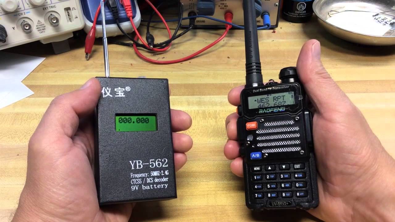
Rotation Counter
Presented here is a simple rotation counter which helps you measure the revolutions per minute (rpm) of any rotating object. As the project requires measurement of very high rpm, a fast-switching device like a reed switch is used. A small round magnet is mounted on the blade as shown in Fig. 1 to activate the reed switch on each rotation. The circuit has been successfully tested up to 6000 rpm but it can measure even beyond that.
Circuit and working
The circuit diagram of rotation counter is shown in Fig. 2. The circuit is built around 5V regulator 7805 (IC1), an opto-coupler MCT2E (IC2), 4-digit counter with 7-segment display driver 74C926 (IC3), four common-cathode 7-segment displays LTS543 (DIS1-DIS4), reed switch (connected at RS1) and a small magnet.
The circuit diagram of rotation counter is shown in Fig. 2. The circuit is built around 5V regulator 7805 (IC1), an opto-coupler MCT2E (IC2), 4-digit counter with 7-segment display driver 74C926 (IC3), four common-cathode 7-segment displays LTS543 (DIS1-DIS4), reed switch (connected at RS1) and a small magnet.
 Opto-coupler IC2 is used to isolate the counter and provide a clock pulse to counter IC3. It counts a pulse when contacts of the reed switch touch each other due to the magnet that comes near it at each rotation. At each rotation, the magnet and reed switch face each other once and the contacts get closed, which causes LED in the opto-coupler to turn on and drive the transistor. This brings clock pulse equal to the number of rotations at the CLK pin 12 of 4-digit counter IC3. IC3 is used to count the clocks received by opto-coupler IC2 and display them on the four common-cathode 7-segment displays (DIS1-DIS4).
IC3 has a 4-digit counter, an internal output latch, npn output sourcing drivers for a 7-segment display and an internal multiplexing circuitry with four multiplexing outputs. The multiplexing circuit has its own free-running oscillator and does not require external clock. The counter advances on negative edge of the clock. A ‘high’ signal on display select (DS) input selects the number in the counter to be displayed; a low level signal on the DS selects the number in the output latch to be displayed.
A maximum of 9999 digits can be counted and shown on DIS1 through DIS4. A high signal at reset pin 13 of IC3 turns all the outputs to zero. So the display shows 0000 when you press the reset switch S2 momentarily.
The power supply used for the circuit is 5V, which is derived from a 12V battery whose voltage is reduced through regulator IC1 to produce 5V regulated power supply. Alternatively, you can use a 12V adaptor for powering the circuit when a battery is not available.

The power supply used for the circuit is 5V, which is derived from a 12V battery whose voltage is reduced through regulator IC1 to produce 5V regulated power supply. Alternatively, you can use a 12V adaptor for powering the circuit when a battery is not available.
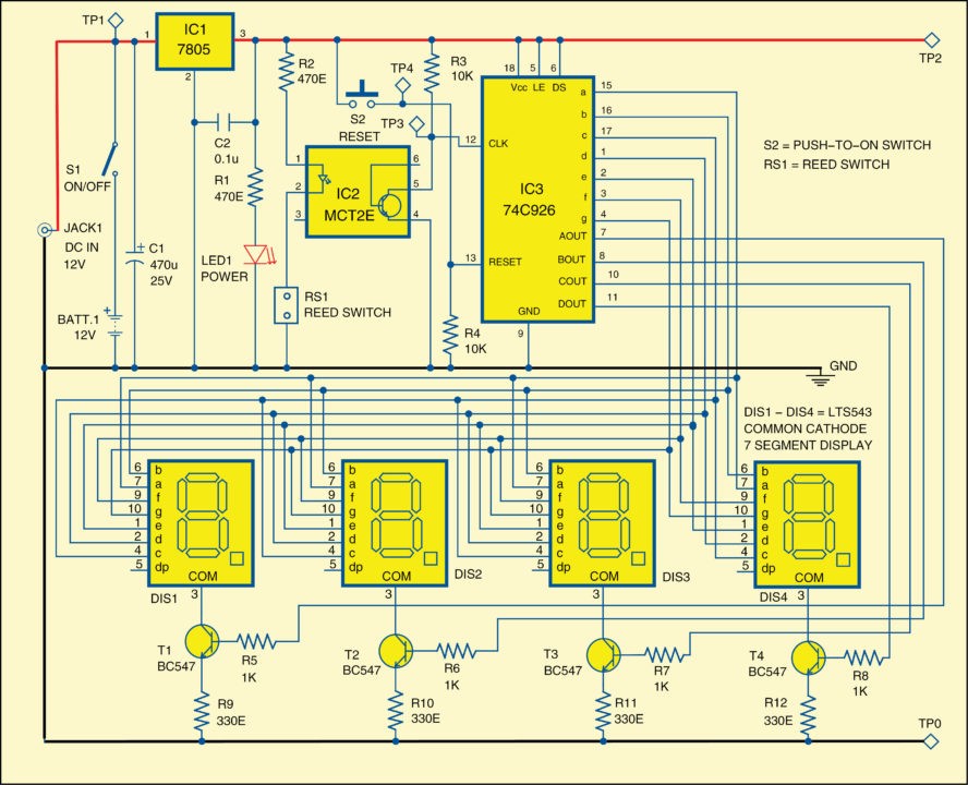
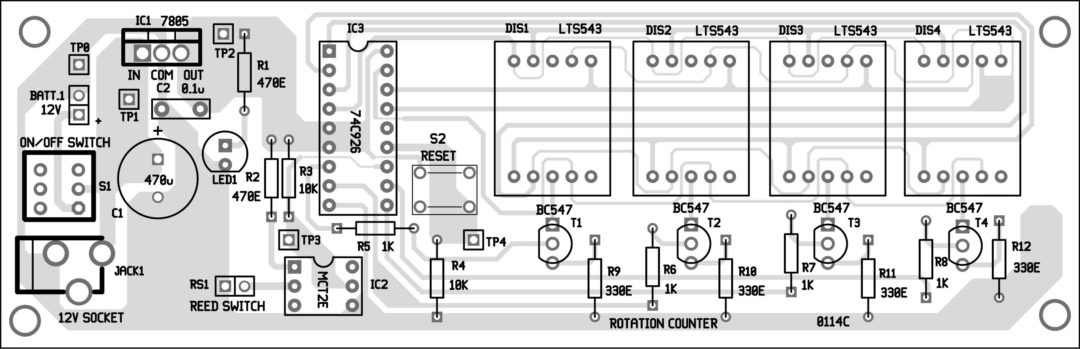
Download PCB and component layout PDFs: click here
Working of the circuit is simple. To count rotations of any rotating object, fix the magnet on the rotating part and rest of the circuit on the stationary part such that the magnet passes close to the reed switch at each rotation. Now press reset switch S2 momentarily. The display shows 0000. Switch on the motor and note the displayed reading after one minute to see the rpm.
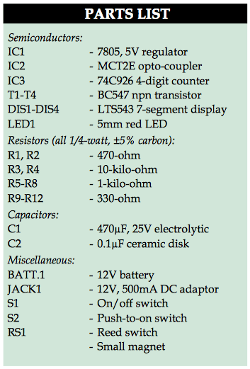
Construction and testing
An actual-size, single-side PCB for the rotation counter is shown in Fig. 3 and its component layout in Fig. 4. After assembling the circuit on PCB, enclose it in a suitable plastic case. After all the components are soldered on the PCB, connect the two wires coming from the reed switch to the main unit.
An actual-size, single-side PCB for the rotation counter is shown in Fig. 3 and its component layout in Fig. 4. After assembling the circuit on PCB, enclose it in a suitable plastic case. After all the components are soldered on the PCB, connect the two wires coming from the reed switch to the main unit.
To check the circuit for proper functioning, verify 12V supply at TP1 and 5V at TP2, with respect to TP0. The clock pulses corresponding to the rotation can be varified at TP3. The reset to the circuit can be observed at TP4. Power LED1 should glow when connected to power supply.

--------_--- ------- GOOD SYSTEM MA THE MATIC -----------_--------------
Tidak ada komentar:
Posting Komentar