L E D ( LIGHT EMITTING DIODE )


X . I Running LEDs Simple
Running LED running lights which are built using LEDs are arranged such that when turned on as it runs. LED running application can be installed as an accessory to the motor or as decorations and ornaments that require animated attractive light. Animated lights that move will surely add to the splendor of the atmosphere of an event or it can also give the impression of creative. One animated lights that are easy to make and not too costly many are running led.
Animation lamp lights or decorations that move is not always expensive and difficult to manufacture. The project is very easy to be made simply by using three pieces of IC CMOS. The circuit is very simple and easy to understand and made his own.
Running LED
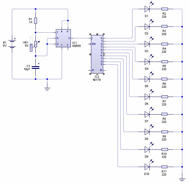
Running LED is made by using two CMOS IC MC14017 as a decade counter. This CMOS IC has the characteristics to enable one bit output alone and able to deliver current up to 10mA. The output current is enough to power a LED with sufficient brightness.
CMOS IC's pretty well it works mainly with supply voltages very wide area of work that began 3.0 VDC to 18VDC. In this case, because when applied to the automotive sector, for example, the selected voltage is 12VDC.
To form the clock pulse used MC14011, a NAND gate CMOS IC. With the potentiometer R3, the output frequency of the clock oscillator can be set.
Directions flame Running LED

Working Principle Running LED circuit
Clock oscillator circuit is built from a series MC14011, R2, R3 and capacitors C2 potentiometer. Operating frequency is set by adjusting the resistance value of potentiometer R3 but if it is still not slow, the value of the capacitor C2 can be enlarged.
The circuit C1 and R1 is a MC14017 circuit reset upon power-up. The first time you turn on the capacitor C1 will fill the cargo so that it appears the voltage across R1 so MC14017 reset. After a while, the capacitor C1 will be full and the voltage on R1 will drop towards 0 volts. In such conditions, the MC14017 will start from the initial conditions where Q0 will be actively followed by Q1 after getting MC14017 clock pulse. After getting 10 times the clock pulse then an automatic MC14017 will reset and return to its initial condition at Q0 active again.
Switches SW1 and SW2 are used to determine the working operations of running this led. If the switch is open then there led yan move. All LED will dwell on the last position. If the switch SW1 is closed then only led D11 to D20 that moved whereas if only the switch SW2 are closed, the only led D1-D10 that moves. But if the second switch is closed, all the LED will move.
Complete Running LED circuit

Running LED circuit development
But if necessary a larger current switching transistor then be added which will be burdened by the led. By using the transistor switching currents to the LED can be adjusted so that more than 10mA. Led the movement direction can be modified as desired. The trick is to put the order led adjusted to the order of its activity. The sequence of activity in 4017 output is in the order of output Q0, Q1, ..., Q10. If the LED brightness is less then the value of the resistor R4 can be replaced menjad 220 ohm LEDs on a circuit that flame became brighter LED running.
X . II Make Alarm Light For Storage
This light alarm circuit serves to provide an indicator in the form of sound when open storage area. Light alarm circuit is created and allocated to the storage of valuables such as safes. Light alarm circuit is very simple but has a pretty good ability to provide an indicator of the opening of the closet / drawer should have covered. Light alarm is activated when it got light.
Complete series of Alarm Light For Storage

Light alarm circuit is the way it works is very simple and its manufacture is not too complicated, simple. From the name it is known that this alarm will work when the detected light. With these functions, the circuit could be used as a burglar alarm or alarm opening the closet / drawer should have covered.
Alarm system Light For Storage
This alarm is activated when the light came on sensor with a particular level of description. Light level setting - dim this can be done by adjusting potentiometer R12. This system has two advantages that comes with time delay alarm activation, setting the buzzer sounds and the detector batteries.
On Delay circuit Alarm Light For Storage

This light alarm circuit using a power source in the form of a 9V battery to be able to carry around, but it is possible to be given power from a power supply of 12V. The circuit in Figure 1 is part of a complete range of light alarm. In Figure 1 is an active alarm delay circuit when the switch SW1 in the 'ON'-kan / on tap.
Given this circuit then allows the user to put this alarm in a closet / drawer before the alarm is active. The circuit in the circuit formed from C1, R1, R2, Q1 and D1. By the time the button SW1, the capacitor C1 will charge charge through R1 so that the base voltage to be down close to 0 volts. This condition will cause the transistor Q1 will be active and forcing the voltage on pin 1 IC 1A will be high.
IC 1 is an inverter gate with schimtt trigger sebanya 6 pieces. IC in a CMOS IC that maximum supply voltage is 18 volts so the current supply voltage (9 V battery or 12V from an external power supply) can still work well.
IC1 pin 1 on the condition that this will cause any high voltage generated by voltage division R3, R12 and R11 (LDR) was unchanged at close to 5 volts.
Some time after the capacitor has been full then the base voltage of Q1 is enough to make Q1 to OFF so that the voltage at pin 1 is really controlled by voltage division between R3, R12 (potentiometer) and R11 (LDR).
So when Q1 is ON, the voltage at the point IC1 pin 1 will be detained remain at around 5 volts and the voltage division between R3, R11, and R12 are ignored. Conversely when Q1 is OFF, the voltage at the point IC1 pin 1 will be determined by the voltage division between the three detainees. Therefore when Q1 is ON then whatever the light conditions (bright / dim) will not affect the system so that the buzzer will always be OFF. If it takes a longer delay, the value of the capacitor C1 can be replaced with slightly larger. The greater the value of the capacitor C1 will cause the delay time will be longer liveliness system.Schmitt Trigger circuit and timer Buzzer In Alarm Light For Storage
Circuit at the front in figure 2 is a circuit to determine the logic state of a light-dark light. With the use of inverters with Schmitt trigger will prevent unwanted trigger.
LDR is a component that has the characteristics in which the resistance value is high when not exposed to light but the resistance value will drop dramatically when the LDR is exposed to light. The amount of impairment LDR resistance is also influenced by the intensity of the light coming into the LDR, the higher the intensity of the light will get low resistance value.
When Q1 OFF and in dark conditions, the voltage at pin 1 of IC1 will be generated from the voltage division between R3, R11 and R12 will generate a voltage high enough, high enough to be considered by the logic inverter gate.
While conversely when in bright conditions, the voltage on pin 1 will be low enough for LDR resistance value is down dramatically. Rated voltage is varied based on the level of light dimming of the light coming into the LDR. This condition can lead to trigger repeated so as to avoid such triggers are used gates with Schmitt trigger, in this system use an inverter gate. Basic election is because it is cheap and in one package there are six gates.
The output of the inverter IC1a own form of logic and can diumpakan directly to the buzzer. However, in Figure 2, in front of IC1a added to the circuit that serves to regulate the way / old sound of the buzzer. When the output of the gate IC1a high then through R4 and C4 (LPF filter) would drive IC1b so the output is low and cause the capacitor C6 unloading. This condition will cause the voltage at pin 5 IC1c will be low for a short time (during capacitor C6 dis-charge) and give a high output to the base of transistor Q2. Active transistor Q2 will cause the buzzer on.
A moment later (after capacitor C6 dis-charge) capacitor C6 will recharge and then the voltage at pin 5 IC1c will rise again from generating low output at the base of transistor Q2, buzzer die. So long active buzzer determined from the length of time dis-charge - charge the capacitor C6 and R6.
But if you'd forever buzzer remain active until the jumper JP3 OFF SW1 may be connected. JP3 connected will force the voltage input pin 3 IC1b be low so that the buzzer will sound continuously even if the LDR is not exposed to light again. Buzzer will die setalh SW1 OFF button. Conversely when jumper JP3 is not connected then the buzzer will sound only when the LDR is exposed to light. After LDR is not exposed to light, the buzzer will not ring.
The detector circuit Low Battery On Alarm Light For Storage

This light alarm circuit using a power source in the form of a 9V battery to be able to carry around, but it is possible to be given power from a power supply of 12V. The circuit in Figure 1 is part of a complete range of light alarm. In Figure 1 is an active alarm delay circuit when the switch SW1 in the 'ON'-kan / on tap.
Given this circuit then allows the user to put this alarm in a closet / drawer before the alarm is active. The circuit in the circuit formed from C1, R1, R2, Q1 and D1. By the time the button SW1, the capacitor C1 will charge charge through R1 so that the base voltage to be down close to 0 volts. This condition will cause the transistor Q1 will be active and forcing the voltage on pin 1 IC 1A will be high.
IC 1 is an inverter gate with schimtt trigger sebanya 6 pieces. IC in a CMOS IC that maximum supply voltage is 18 volts so the current supply voltage (9 V battery or 12V from an external power supply) can still work well.
IC1 pin 1 on the condition that this will cause any high voltage generated by voltage division R3, R12 and R11 (LDR) was unchanged at close to 5 volts.
Some time after the capacitor has been full then the base voltage of Q1 is enough to make Q1 to OFF so that the voltage at pin 1 is really controlled by voltage division between R3, R12 (potentiometer) and R11 (LDR).
So when Q1 is ON, the voltage at the point IC1 pin 1 will be detained remain at around 5 volts and the voltage division between R3, R11, and R12 are ignored. Conversely when Q1 is OFF, the voltage at the point IC1 pin 1 will be determined by the voltage division between the three detainees. Therefore when Q1 is ON then whatever the light conditions (bright / dim) will not affect the system so that the buzzer will always be OFF. If it takes a longer delay, the value of the capacitor C1 can be replaced with slightly larger. The greater the value of the capacitor C1 will cause the delay time will be longer liveliness system.
Schmitt Trigger circuit and timer Buzzer In Alarm Light For Storage
Circuit at the front in figure 2 is a circuit to determine the logic state of a light-dark light. With the use of inverters with Schmitt trigger will prevent unwanted trigger.
LDR is a component that has the characteristics in which the resistance value is high when not exposed to light but the resistance value will drop dramatically when the LDR is exposed to light. The amount of impairment LDR resistance is also influenced by the intensity of the light coming into the LDR, the higher the intensity of the light will get low resistance value.
When Q1 OFF and in dark conditions, the voltage at pin 1 of IC1 will be generated from the voltage division between R3, R11 and R12 will generate a voltage high enough, high enough to be considered by the logic inverter gate.
While conversely when in bright conditions, the voltage on pin 1 will be low enough for LDR resistance value is down dramatically. Rated voltage is varied based on the level of light dimming of the light coming into the LDR. This condition can lead to trigger repeated so as to avoid such triggers are used gates with Schmitt trigger, in this system use an inverter gate. Basic election is because it is cheap and in one package there are six gates.
The output of the inverter IC1a own form of logic and can diumpakan directly to the buzzer. However, in Figure 2, in front of IC1a added to the circuit that serves to regulate the way / old sound of the buzzer. When the output of the gate IC1a high then through R4 and C4 (LPF filter) would drive IC1b so the output is low and cause the capacitor C6 unloading. This condition will cause the voltage at pin 5 IC1c will be low for a short time (during capacitor C6 dis-charge) and give a high output to the base of transistor Q2. Active transistor Q2 will cause the buzzer on.
A moment later (after capacitor C6 dis-charge) capacitor C6 will recharge and then the voltage at pin 5 IC1c will rise again from generating low output at the base of transistor Q2, buzzer die. So long active buzzer determined from the length of time dis-charge - charge the capacitor C6 and R6.
But if you'd forever buzzer remain active until the jumper JP3 OFF SW1 may be connected. JP3 connected will force the voltage input pin 3 IC1b be low so that the buzzer will sound continuously even if the LDR is not exposed to light again. Buzzer will die setalh SW1 OFF button. Conversely when jumper JP3 is not connected then the buzzer will sound only when the LDR is exposed to light. After LDR is not exposed to light, the buzzer will not ring.
The detector circuit Low Battery On Alarm Light For Storage
This system was designed by using the power supply from the battery and therefore need to be made in order to dketahui detector batteries when the battery is used tesebut are not eligible to be replaced. The battery voltage is too low can cause the alarm system misunderstand light-dark light. In addition buzzer sound will be increasingly ketch and weak.
As in Figure 3, the detector battery is constructed from a series D7 and R10. When the battery voltage (VCC) above 4.3 volts then there is still a leakage current to the R10 and sufficient to cause the voltage on pin 9 IC1d high. This condition will cause the oscillator formed from a series of IC1e, R9, C8, C5, and R8 do not work causing the voltage at pin 13 IC1f high. This will cause Q2 OFF and only depends on IC1c.
Conversely when the battery voltage is below voltage of 4.3 volts then there is no leakage current to the R10 so that the voltage on pin 9 will be close to 0 volts and is considered a logic low. This condition causes the active oscillator so pin 13 IC1f will receive the pulses from the oscillator so that Q2 will be active as well. Pulses generated by IC1f will activate Q2 although IC1c also active.
It later the sounds with a fusion of sound with a higher frequency sound of buzzer when the system gets enough light.Sensitivity settings LDR circuit Alarm Light For Storage tempan
LDR sensitivity settings set using a potentiometer R11. In the initial settings, position potentiometer halfway down. Then put the light on the place that you want to detect and adjust the potentiometer that produces sound when it gets light and not to sound when the system does not get light.
Pengatikfan buzzer duration is determined by the value of C6 and R6, for a longer time are advised to replace the value of the capacitor with a higher value.
For larger buzzer, which requires a greater flow of transistor Q2 can be replaced with Darlington transistor which has a larger collector current. Note the current consumption of the buzzer and the current capability is able to pass by the collector on the transistor Q2.
Light alarm circuit for a storage area above, supplied with 9 volt batery and equipped with a detector low baterry. So in addition to having high sensitivity to changes in light with meberikan sound when exposed to light, when the baterry energy light alarm circuit is running out for this storage will also be sounded.
X . III Lights Disco (Disco Lite) Using Microcontroller
Lights Disco (Disco Lite) Using Microcontroller
Under the control of AT89C2051, as many as 256 lamps 'dancing' in tune with the audio signals received this tool.
Compared with AT89C51 which has 40 foot, 20 foot reduced IC AT89C2051 AT89C2051 this resulted only has 2 pieces Port, the Port 1 and Port 3. In addition, the capacity of Flash PEROM in only 2048 bytes AT89C2051, AT89C2051 PEROM half-capacity Flash.
Nonetheless, AT89C2051 analog comparator has not owned AT89C51. Analog comparator is an electronic circuit to compare two voltages, the existence of this facility can be used to monitor voltage AT89C2051 analog (voltage instead of digital) directly, for example, be used as an Analog / Digital Converter is simple.The series of lights Disco (Disco Lite) Using Microcontroller
Figure 1 shows the complete range of Disco Lite, AT89C2051 is equipped with a capacitor C1, C2 and Y1 as a 12 MHz crystal oscillator circuit, a capacitor C3 and resitor forming reset circuit.
Disco circuit Lite

Resitor R17, R16 and a capacitor C4 and capacitor C5, C6, diode D1, resistor R36, R37 along with AT89C2051 form a series of Analog / Digital Converter is simple, is used to measure the magnitude of the incoming audio signal.
Another part of the circuit consists of two pieces of 74HC573, 2 pieces 74LS164, 32 resistors and transistors 16, and a 16 × 16 Dot LED Display Panel. This section is part of the display, the Display Panel measures about 8 x 8 cm that there are 256 pieces of LED Flash / outage adjusted to the rhythm of the received audio signal.
Audio signals received on-the-scale into 10 parts according to the size of the signal, each section has a pattern flame scale / taps different lights, so the strength of the audio signal will form a random image on the display panel.
The equivalent circuit Analog / Digital Converter

Figure 2. The equivalent circuit Analog / Digital Converter
Figure 2 illustrates an equivalent circuit Analog / Digital Converter, before being measured audio signals received conditioned first, potentiometer R36 is used to adjust the size of the level of audio signals received, because the circuit Analog / Digital Converter only accept voltage positive then the audio signal is rectified by the diode D1 , while the resistor R37 and capacitor C6 is a simple filter to slightly dampen the audio signal that is not too volatile.
The voltage of the audio signal is fed to the foot of the AT89C2051 P1.1 which serves as input V- (inverting input) from Analog Comparator.
P1.0 foot which serves as input V + (non-inverting input) is connected to a capacitor C4, the capacitor is charged via R17 and R16 custody at the time AT89C2051 P3.7 of the state '1', and the contents emptied through R16 when P3.7 in a state of '0'.
Shape voltage across the capacitor C4 (connected to P1.0) during capacitor charging and discharging the capacitor shown in Figure 3.

Figure 3 .Graph capacitor voltage
At the start measuring voltage audio signal, the capacitor C4 to be empty or the capacitor voltage = 0 volts, the voltage is more positive than the P1.0 P1.1 so that the output of the Analog Comparator (P3.6) = '0'.
After that P3.7 = '1', the voltage across the capacitor C4 starts to rise in accordance with the charts Figure 3, until such time as the C4 voltage more positive than the audio signal and output voltage Analog Comparator P3.6 changed from '0' to '1'. The time interval when it begins charging the capacitor to P3.6 to '1' is equivalent to the voltage audio signal, the greater the longer the voltage P3.6 to '1'.
On / off LED 256 is set by means of multiplex, as used in the article Digital Clock With AT89C2051. Borrowing terms are used in the article, 16 × 16 Dot LED Display Panel used can be considered a viewer with 16 segments of 16 digits.
16 pieces each digit switch is formed by a resistor and PNP transistor, because the amount exceeds the AT89C2051 foot can not be controlled directly via the existing port, but through the help of two pieces of IC 74HC573 (contains 8 pieces Latch). Data stored into two IC is fed from P1.2..P1.7 and P3.2..P2.3, P3.4 used to organize the first 74HC573 (U2) if P3.4 = '1' then the data in this IC input will be recorded and passed to the output, P3.4 to set the second 74HC573 (U4).
16 pieces switch segment is formed by two pieces of IC 74LS164 (containing 8 bit shift register), the resistor is mounted on the IC output is used to limit the LED current. Data segment as many as 16 bits sent from AT89C2051 in series, shifted into the shift register 74LS164. When the data is shifted, all switches digit is turned off so that the shifting process is not visible on the display
Working Principle Lights Disco (Disco Lite) Using Microcontroller
Disco Lite program flow diagram shown in Figure 4, after this tool gets the power supply directly carry out the program of preparation to organize the work of the tool, things to do, among others, first turn off all the lights display, empty capacitor C4.
Main part of the program is set up to see which is formed from a 256 point LED, the data segment that will be displayed is sent to the display system via two pieces of IC shift register 74LS164, after it skaklar digit corresponding to the data segment of the newly delivered ignited. This process is done continuously for the tool to work, so that the display does not wobble begian look good is to be done fairly quickly.
After 50 rounds of the appearance setting process, this process left briefly to measure voltage audio signal, on the basis of the size of the measured voltage selected pattern on / off lights that had been prepared first in Flash PEROM, and the pattern will be displayed.
Effect lights formed, can be easily composed and filled into Flash PEROM so that it can be formed various models of performances by the Lights Disco (Disco Lite) Using the Microcontroller.
X . IIII Picture Matrix LED Display
Picture Matrix LED Display
Means display today are very much among others, cathode ray tube, liquid cell display, LED matrix, and so forth. Picture this matrix LED display will show the pictures with the Microsoft format Bitmap (BMP) into the matrix LED pixel size of 16 X 16 pixel black and white.
Use of this tool is very simple, it requires a personal computer and the device itself. Sending data from the tool to the PC is done via serial communication port on the PC that is connected to the device via the MAX232. The device uses two pieces of the program which is a program written in Turbo Pascal for the processing of BMP images before sending and assembly programs written with AIDS to display images that are sent to the device. Block diagram of the device can be seen as follows:
Scheme Block Diagram, Picture Matrix Led Display

Before discussing further, will recognize the file structure dalu Windows Bitmap (BMP). This file is a graphic file without compression. First of all for each file always contains a header record, for BMP files, there are 15 kinds of information including the type of BMP, file size, width, length, color, horizontal and vertical resolution, and so forth. Everything can be seen in Pascal existing program. BMP file header contained in forward while the next image data representing pixels and colors. For the first pixel BMP files left over there on the left past the bottom so that the BMP file is written upside down so as to be read from the back first, or more precisely from the bottom left to right and up to the left again it continues until the top left of the first.
There are three important parts in this block to be noticed, yalmi serial interface block, block and block scanning display processor. These three blocks plays an important role on this device.
Through the serial interface will occur serial data transfer from the computer to the MCS-51, so that the signal level of MCS51 series of data equivalent to the signal level of communication ports on your PC, MAX232 required to change the voltage to the TLL / CMOS logic-level RS232.
Pin 12 (RXD) on the MAX232 will go to pin 2 (P3.0) on the MCS-51 and pin 11 (TXD) will go to pin 3 (P3.1) on the MCS-51.
The circuit of the system can be seen as follows:
MAX232 RS232 to Logic Level Converter

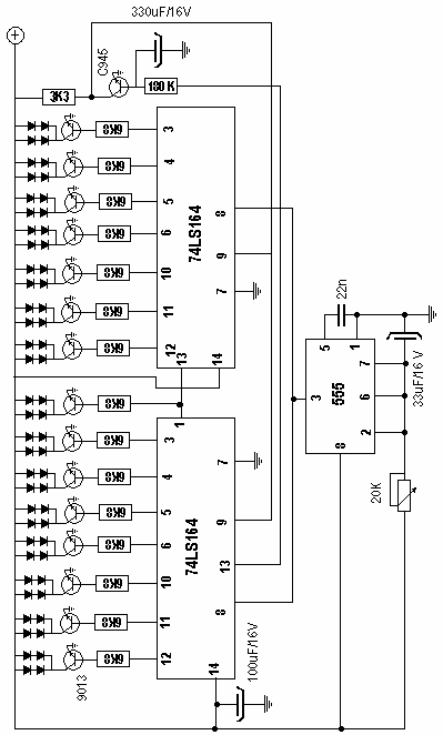
Block processors can be observed as follows. This block is the brain of the system matrix led display this picture, because all the inputs and outputs to be issued shall be processed and controlled via IC AT89C2051. This IC receives data from a PC via the RS232 channel scanning display and arrange for care of the display on LED matrix display. All legs on AT89C2051 is used for serial transfer, data is output to latch, latch controllers, input to the SIPO, SIPO clock controller, so that the only remaining one leg that is not used is P 3.7. IC is equipped with a 11.0592 MHz crystal and 2 pieces of capacitor (C1 & C2) to form a series oscillator and reset circuit in the form of capacitor (C3) with a resistor (R17).
Serial input of the MAX232 entered as RXD P3.0 and P3.1 as TXD, P3.2 and P3.3 as a regulator 74HC573 latch enable as much as 2 pieces, P3.4 as a regulator clock at SIPO IC 74LS 164 as much as 1 piece and P3 .5 as input data on a 74LS164. P1.0 to P1.7 as input data to the 74HC573 latch. Keep in mind that while the device is working, the First of all it will do is reset first. This device will not be reset before the on-off-the then-on-kan again.
The series of these blocks can be seen as follows:
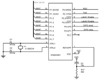
Figure 3 . processor block
For the purposes of scanning requires only two pieces of IC 74LS573 latch and 2 pieces of SIPO IC 74LS164. Controlling 4 IC is controlled directly by the AT89C2051. Controlling includes latch when this is enabled, when the SIPO and the data given in clok and others.
Scanning system display can be seen from the order of the program as follows, first of all the data taken at the address $ 40 and then latch 1 active're latch 2 is either disabled, after which it moved to P1untuk sent to latch, as well as to the data to latch onto 2, where the latch 1 in off so that the incoming data to latch onto 2. Shift_data be set high so that the output SIPO low with the aim that led to life later in the clock for 15 times that of the low data is moved as much as 15 times so that the scanning process runs in a loop until then there are other data.
Transistors used are BC557 (PNP), this transistor will be on-kan when it gets input from the latch so that the flow from the emitter to the collector directly and then to 470 ohm resistor and LED matrix display. Transistors are used as many as 16 pieces. To SIPO 74LS164 controlled by AT89C2051, after receiving the input clock given that data on QA can be shifted to the QB and so on. Need to be observed as well as the first IC 74LS164 completed or has reached QH then this output will be the input for the second 74LS164 so that it will continue. If the output of the transistor and the SIPO is met then the LED will light up. To avoid ghosting after 1 byte LED is turned on, before moving onto the next one byte led off beforehand so that ghosting can be avoided.Working Principle Picture Matrix LED Display
The series of Led Matrix Display Device Picture

The working process of the device is very simple, first of all need to open the Turbo Pascal program first and then run a program that already exists. The initial appearance of the program is going to ask the bmp file which will be processed to be transferred, it is necessary for charging the exact location of the files and their directories and sub-directories if any. Existing files must qualify that must file with bmp extension pixel size of 16 x 16 pixels and will have two colors: black and white. If the selected file does not qualify then the program will refuse that if the file is not bmp bmp and if this file will be checked whether the file is 16 x 16 pixels 2 color otherwise it means that instead of 16 x 16 pixels.
If the selected file already qualified then this program will continue next instruction is read the file, retrieve data, and then transferred serially to the picture matrix LED display system. Because MCS51 is already programmed, the incoming data will be immediately displayed to the LED matrix display. The data transmitted only takes in seconds to be able to perform to the LED matrix display. Next will show the files to be transferred later. This program will continue to repeat until stopped manually.
After knowing the things above it can use the device properly and can develop later for various purposes and can be developed device is also an example in all things may be reproduced matrix led with a note should be added a few pieces of IC, and so forth. Disadvantages of this device include images that can be processed quite small, only 16 x 16 pixel black and white but this device is simply the basis for the development of the device itself.
X . IIIII Using Flash Automotive LED
The flash is automotive fittings or accessories that are familiar to automotive enthusiasts. However, using the LED flash with a very bright flame and blue instead of the flash may be created as an alternative to the real flash.Flash Automotive
It uses LED flash that is not as bright as the use of the flash, but there are advantages that are cheaper and not too large use of electric power. The circuit is very simple so peletakannya unobtrusive. In addition the circuit has been designed to use a 12V supply voltage, adjustable voltage accumulator on the car.Ultra Bright LED Flash For Automotive
Colors are suitable for this project is that the bright colors are produced by ultra bright indeed led to led this type are more expensive than regular LED. This type of ultra bright LED has a brightness which is higher than usual and led the colors are common in the market are blue, red and green.
Forward bias characteristics, to turn on the LED is the same as usual which led anode should be more positive than the cathode and current is set between 20mA to 50mA.
Application of flash this one is on the car accessories. The flash will be able to effect the brightest flashes when placed in a reflector lights right at the focal point. Peletakannya is not necessarily so because it would interfere with the lights if it is still in use.Working Principle of Flash Automotive Networks
Led will emit bright light when energized 20mA minimum within a certain time. However, if the LED is done in pulses with very small duty cycle will not produce a flash of bright if you use only 20mA current.
There are two alternatives to solve this problem is to enlarge its duty cycle with the current fixed at 20mA or remain on duty cycle is small but using currents greater than 10x normal flow.
This can be explained like this, if the LED is turned with a pulse that has a duty cycle of only 1%, the current average is only 20mA * 1% is only 0.2mA, a very small current to power the LED with the brightness expected. But instead by using currents of up to 2A, the average current passing through the LED is only 20mA (using a 1% duty cycle) with the magnitude of the instantaneous current of 20mA is enough to power the LED brightness is good enough.
It is still possible because LED has the characteristics of forward bias current is 20mA to 50mA continuously. And these characteristics do not apply to the instantaneous current which has its own limitations, namely the parameters of non-repetitive surge current where values up to 10A.
Using a series of Flash Automotive LED

Figure 1
Using a series of Flash Automotive LED
Basically, the circuit in Figure 1 is an oscillator circuit formed by LF351. Opamp LF351 is built from the FET so as to have a very high imoedansi and well suited to use in the oscillator. In addition to determining the pulse width at this LF351 on foot created as a non-inverting comparator.
Basically, the circuit in Figure 1 is an oscillator circuit formed by LF351. Opamp LF351 is built from the FET so as to have a very high imoedansi and well suited to use in the oscillator. In addition to determining the pulse width at this LF351 on foot created as a non-inverting comparator.
Shape Signals and Signal OutputBentuk Oscillation Oscillation Signals and Signal Output

Figure 2
The comparator compares the voltage oscillation signal (Figure 2 above) with particular reference voltage. The reference voltage is built using a voltage divider R1 and R2. While
the R8 potentiometer is used to adjust the frequency of the oscillator
so directly set the frequency of the flashes of the LED lights. For
the duty cycle of the pulses formed of LF351 is made remains with the
intent to keep the average current flowing to the LED stays around 20mA.
Increased pulse duty cycle is needed resetting current limiting resistance to LED. If
the duty cycle of its enlarged the average current flowing to the LED
will be greater so that the resistance value needs to be improved. If the LED current limiting resistance is not raised then the current can damage the LED.
The oscillator built in Figure 1 is a relaxation oscillator in which the initial operation is to make the filling (charging) capacitors C2 and then discard (discharge) the charge resulting signal as in figure 2 the top.
LF351 also berfugsi as a voltage comparator where the reference voltage is set by the circuit R1 and R2. When the voltage at the inverting pin is lower than the voltage at the non-inverting pin (reference voltage), the output LF351 will produce high pulse but instead when the voltage inverting pin pad is higher than the reference voltage, the output LF351 will generate a low pulse.
Resistors R1 and R2 form a voltage divider that divides the right voltage at non-inverting pin in the middle of the supply voltage. But with the series potentiometer R8 and R3 will change this voltage. So in other words, changes in the value of the resistance on the potentiometer will cause the voltage of the division of R1 and R2 will change. When outputLF351 high then this voltage will rise if output LF351 low while the voltage will go down anyway.
The amount of charging the capacitor is determined by pengaturang by potentiometer R8. When the resistance value of the potentiometer R8 ride the charging of C2 will decrease and vice versa.
At first C2 has no charge and output LF351 will be high. A moment later C2 will fill the charge of output LF351 who was in a state of high through R4. R5 and the diode D3 provides lower resistance so that the faster charging C2 until the voltage approximately above bias voltage non-inverting pin. At the moment in the output of LF351 will be low and C2 will dump its load only through R4. The series of R5 and D3 can not flow in this disposal so that the discharge will be longer than the filling.
For the LED driver used TIP122 or can have another one of the type transistor Darlington and was able to spend at least 2.5A flows continuously so that the flash can emit light automotive optimally.
X . IIIIII Know Robot And Characteristics
Robots are complex and difficult to describe in words. Robots are usually programmed to do the work repeatedly and have a mechanism that is guided by automatic controls. While robotics is basically the study of robots, so that robotics is defined as the branch of technology that deals with the design, construction, operation, and application of robots. Robotics is a branch of science that studies on robot. The branch of science includes machine design robots, electronics, control, computer programming, artificial intelligence, and so forth.

definition Robot ( ROBO = Ringing on Boat )
There are some opinions of experts gave the definition of a robot in a robot. Based on some of the references obtained several definitions robot as follows.
In the Meriam-Webster dictionary definition of robot is a machine that looks like a human being and performs various complex acts of human beings as walking or talking, or a device that works automatically.
Robotic Institute of America is an institution robots at Carnegie Mellon University in 1979 made the definition manipulator robot is multi-functional and can be reprogrammed designed to move material, tools, or specialized devices through a number of movements programmed to perform certain activities.
Basic Characteristics Robot
The robot has four basic characteristics, so that we can more easily determine whether an object is a robot or not to know the basic characteristics of the object. Four basic characteristics or parts of robots that must exist or be possessed by each robot are:
Robot Having a sensor
The sensor is a useful tool to measure or feel something in the environment outside the robot, like the sense in living things, and report the results to a robot. With the sensor, the robot could have a consideration in the decision. Examples of the sensor is a light sensor to detect the presence of light and temperature sensors for measuring temperature.
Robot Has (Control) system intelligence
Intelligence system works by processing the input data in the form of circumstances or events that are happening from the outside environment. Then the system generates output in the form of instructions or a decision on the robot to perform a particular action. This system generally has a working principle as the brains of living creatures, which serves to think and decide what action needs to be taken at a certain time.
Robot Has (Actuator) mechanical equipment
Mechanical equipment used to make the robot can perform a certain act and interact with their environment. Examples such as the motorized wheel to move, arm to grab objects, and others.
Robot Having a (Power) resources
As well as living beings who need food to live, robots also need a power source to drive the electrical and mechanical components are attached. The energy source for robots include electricity providers such as batteries, and transmission control systems that convert electricity charge according to the needs of each component.
In modern robots, actuators are often associated with mechanics. In mechanics, learned things about various styles that occur as a result of the arrangement of construction, the location of the center of gravity, and material properties. Taking into account the properties of mechanics, the robot will move with a stable and reduce the risk of falling.
Sensors on the robot is often related to the science of modern electronics. In the science of electronics studied matters related to electronic components, analog circuits, digital circuits, and microcontroller. A sensor may be composed of a series of analog or digital circuits. Along with the increase in computer and electronics technology, the increased development will be sensors that can be fabricated with the mini size.
Intelligence systems on modern robot developed in a software. Artificial intelligence can be designed using an algorithm that allows the robot to move automatically, taking into account the information about which is read from the existing sensor. In addition there is a connectivity layer between intelligence system with sensors and actuators. Thus, data can be transferred between components managed by hardware using software created for the robot
Another example: Led Networks walk is actually the development of logic flip-flop that is the basis of Sequential Logic Networks. Sequential circuit is a logic circuit which has an output that is not dependent on the inputs but also on its output as well. In addition, sequential logic circuit can remember the logic that we run.
The series:
X . IIIIIII Walking With the lamp circuit Transistor
The series of running lights is a simple electronic circuit that functions to control the LEDs forming the display runs. The series of running lights with these transistors can be used to control the LED lights turn on and the light bulb DC. The series of running lights can be operated with a DC voltage source of 12 volts to 24 volts corresponding weight. To create a string of running lights with these transistors can be seen schematics and components that are used as shown below.
List of circuit components Lamp Walking With TransistorR1 = 1K5R2 = 680RC1 = 47μF 25VD1 = LEDQ1 = BC337P1 = SPSTLP1 = 12 or 24V Lamp
Running lights with transistor circuit in the image above can be added up to the desired number of lights, running lights with a transistor circuit in the picture above is simple, easy to apply and easy modification.
Period lights on the circuit with a transistor running lights above was determined by the time of charging and discharging the capacitor C1. The speed of charging and discharging the capacitor C1 in the circuit running lights above will be faster if the value of the capacitor is getting smaller, and more slowly if the capacitance value of the capacitor C1 increases. To use a lamp load DC power it needs to be taken into account, the light used with a capacity of transistors in a current on the collector emitter transistor digunakan.Apabila used lapu load large power transistor used must also disesuakan then mounted cooling (heatsink) because the transistor will issue hot.
X . IIIIIIII The series of LED lights
LED lamp circuit is a circuit that contains some components LEDs connected in series or parallel which usually consists of components of the input voltage, electric current, LED, resistor and resistor as current if the current flowing from the source is too large for the size of the LED. LED (Light Emitting Diode) is a kind of semiconductor diode component which will produce a space depletion or P-N junction, when the electron and hole flows to the junction with different voltages, the electron will release energy photonnya because the electron energy in the lower level. LED lighting circuits themselves have developed not only a series of LED switches again, but has been developed for application logic signal for the LED.
Figure Schematic circuit LED Lights

At
the installation of LED lighting circuits in series sought wherever
possible to use LED components of the type and the same color in order
to avoid differences in the forward voltage of each LED. Because
if a series circuit then all the components should get the same voltage
value, and when will there is a difference in voltage, it is feared the
instability voltage is supplied by a source. Factor
that will result when the applied voltage is low, then later there is
an LED component that will not start because of different voltages. Conversely, when a voltage entered is too big because of the
instability it will cause a voltage division LED components will be
damaged or broken.
As with the installation of lighting circuits in parallel, on a highly parallel strings of LEDs to note that the current sharing of each component and the ramifications. Similarly, the series that has its voltage instability, then in parallel instability that occurs in the current division. So why should we use a mixture of the circuit to design a series of LED lights if we want to design a system that uses LED circuit logic. For example in the case of LED running we should really pay attention to the time distribution of current and voltage evenly. To reduce the occurrence of instabilities enter the LED goes it is used IC COUNTER mounted on a series of LED lights.
As with the installation of lighting circuits in parallel, on a highly parallel strings of LEDs to note that the current sharing of each component and the ramifications. Similarly, the series that has its voltage instability, then in parallel instability that occurs in the current division. So why should we use a mixture of the circuit to design a series of LED lights if we want to design a system that uses LED circuit logic. For example in the case of LED running we should really pay attention to the time distribution of current and voltage evenly. To reduce the occurrence of instabilities enter the LED goes it is used IC COUNTER mounted on a series of LED lights.
X . IIIIIIIII How to Make the Long Walk Led (cascade)


This circuit utilizes two pieces of 4017 and 10 of transistors that will create 25 pieces of led walks, and if you like can be extended up to 10 x 10 or 100 pieces. This circuit utilizes a combination of scanning the columns and rows as well as dot matrix, but if the LEDs are arranged in sequence then the maximum 100 sequences can be obtained.
The basic circuit of running 10 LED as follows:

Whereas if at cascade 2 pieces 4017 how by adding a diode and some resistors.

This cascade circuit utilizing the clock output from the pin to the first third of 4017. Sometimes smart people too much harm and circuit above does not work to try lhoo. The author finally experimenting so finding a more accurate way by using a transistor as a control input pin to enable and reset as the following circuit.
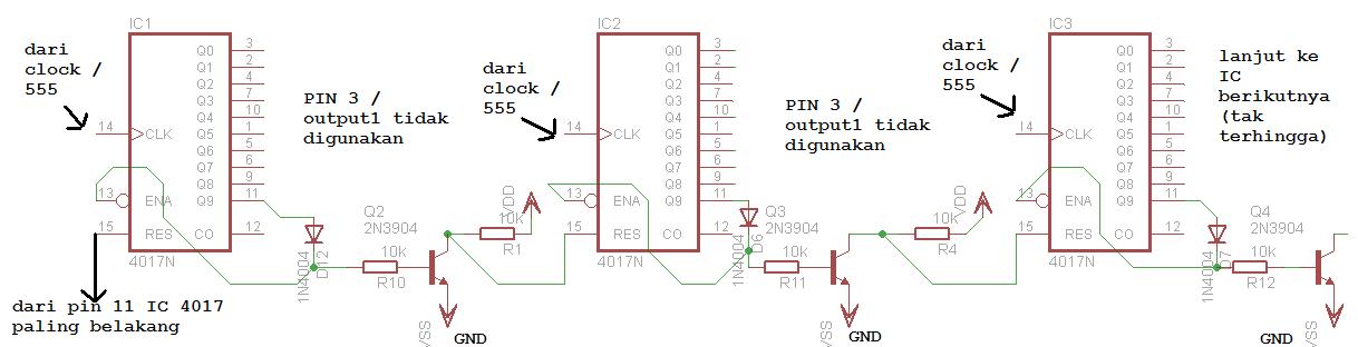
(Click to enlarge, VDD = Voltage (+) VSS = Voltage (-) or Ground)
Additional components such as 1N4148 diodes, resistors 10K and general NPN transistor like 2N3904, BC107, 2N2222, C9013 and so forth. The clock input of the circuit is derived from the clock circuit 555 (or any others) was given to each ic 4017.
The principle of the series is to give input to pin 13 (chip enable active LOW) on the last sequence (Q9) of an IC 4017. During the sequence has not ended then Q9 whose value is "LOW" will mengenable the IC and me-Reset IC on the next position , The effect is that only a 4017 that will be active while ic 4017 after being in a state of "Reset" while in 4017 ic previous position get position disabled.
This circuit can be made up to 4017 infinitely many, and at last ic 4017, the last sequence (Q9) will be connected to the first reset in 4017 ic. Should do given diodes that logic is floating (float). This condition will reset all ic 4017 and start the sequence over again. The output is Q0 and Q9 sacrificed so reduced by 2 pieces of sequence per ic 4017.
Trick cascading is very useful for the process of scanning the columns for a series of text scroll led matrix using a polynomial as the discussion here.
Another fairly simple way is to utilize such ic shift register 74LS595 / 74HC164 but ic shift register would be difficult to be found in the peripheral areas so that ic 4017 more universal becomes the best option.

16 (or more) Stage LED Sequencer
Circuit in the picture above using a hex inverter Schmitt Trigger (74HC14) and two 8-bit Serial-In / Parallel-Out shift register (74HCT164 or 74HC164) for the order of 16 LEDs. The circuit can be expanded to greater lengths by cascading additional shift registers and connects to the output-8 (pin 13) to the data input (pin 1) the next stage. a Schmitt trigger oscillator (74HC14 pins 1 and 2) generate a clock signal to the shift register, with a clock speed that is approximately 1 / RC. Two additional stages of the Schmitt trigger is used to reset and load registers when ignited. Timeliness not need too much attention, but output on pin 8 of Schmitt Trigger must remain "HIGH" during the "LOW" or 0 of the first and is used to transition the clock to "high" at pin 8 from the register, and shall return "LOW" before clock rising edge to load a bit. If the clock rate increases, the length of the signal on pin 9 of Schmitt Trigger reduced proportionately to avoid including more than one bit. IC with type HC will typically provide about 4 mA (called sink current) of each output but can supply large currents (perhaps 25 mA) if only one output is loaded. Generally the 150 ohm resistor limits the current is below 25 mA when using a 6 volt power source. If this circuit is operated by two or more LEDs at the same time, it may take a resistor in series with each LED to avoid exceeding the total maximum output current for each IC of 25 mA. For greater brightness, transistor buffer / power can be used as has been discussed in the design of LED running 10 stage in here .
Circuit in the picture above using a hex inverter Schmitt Trigger (74HC14) and two 8-bit Serial-In / Parallel-Out shift register (74HCT164 or 74HC164) for the order of 16 LEDs. The circuit can be expanded to greater lengths by cascading additional shift registers and connects to the output-8 (pin 13) to the data input (pin 1) the next stage. a Schmitt trigger oscillator (74HC14 pins 1 and 2) generate a clock signal to the shift register, with a clock speed that is approximately 1 / RC. Two additional stages of the Schmitt trigger is used to reset and load registers when ignited. Timeliness not need too much attention, but output on pin 8 of Schmitt Trigger must remain "HIGH" during the "LOW" or 0 of the first and is used to transition the clock to "high" at pin 8 from the register, and shall return "LOW" before clock rising edge to load a bit. If the clock rate increases, the length of the signal on pin 9 of Schmitt Trigger reduced proportionately to avoid including more than one bit. IC with type HC will typically provide about 4 mA (called sink current) of each output but can supply large currents (perhaps 25 mA) if only one output is loaded. Generally the 150 ohm resistor limits the current is below 25 mA when using a 6 volt power source. If this circuit is operated by two or more LEDs at the same time, it may take a resistor in series with each LED to avoid exceeding the total maximum output current for each IC of 25 mA. For greater brightness, transistor buffer / power can be used as has been discussed in the design of LED running 10 stage in here .
X . IIIIIIIIII 28 Led Clock Timer electronic circuit diagram

This is a programmable clock timer circuit that uses individual LEDs to indicate hours and minutes. 12 LEDs can be arranged in a circle to represent the 12 hours of a clock face and an additional 12 LEDs can be arranged in an outer circle to indicate 5 minute intervals within the hour. 4 additional LEDs are used to indicate 1 to 4 minutes of time within each 5 minute interval.
The circuit is powered from a small 12.6 volt center tapped line transformer and the 60 cycle line frequency is used for the time base. The transformer is connected in a full wave, center tapped configuration which produces about 8.5 volts unregulated DC. A 47 ohm resistor and 5.1 volt, 1 watt zener regulate the supply for the 74HCT circuits.
A 14 stage 74HCT4020 binary counter and two NAND gates are used to divide the line frequency by 3600 producing a one minute pulse which is used to reset the counter and advance the 4017 decade counter. The decade counter counts the minutes from 0 to 4 and resets on the fifth count or every 5 minutes which advances one section of a dual 4 bit binary counter (74HCT393). The 4 bits of this counter are then decoded into one of 12 outputs by two 74HCT138 (3 line to 8 line) decoder circuits. The most significant bit is used in conjunction with an inverter to select the appropriate decoder. During the first eight counts, the low state of the MSB is inverted to supply a high level to enable the decoder that drives the first 8 LEDs. During counts 9 to 12, the MSB will be high and will select the decoder that drives the remaining 4 LEDs while disabling the other decoder. The decoded outputs are low when selected and the 12 LEDs are connected common anode with a 330 ohm current limiting resistor to the +5 volt supply.
The 5th output of the second decoder (pin 11) is used to reset the binary counter so that it counts to 11 and then resets to zero on the 12th count. A high reset level is required for the 393 counters, so the low output from the last decoder stage (pin 11) is inverted with one section of a 74HCT14 hex Schmitt trigger inverter circuit. A 10K resistor and 0.1uF cap are used to extend the reset time, ensuring the counter receives a reset signal which is much longer than the minimum time required. The reset signal is also connected to the clock input (pin 13) of the second 4 bit counter (1/2 74HCT393) which advances the hour LEDs and resets on the 12th hour in a similar manner.
Setting the correct time is accomplished with two manual push buttons which feed the Q4 stage (pin 7) of the 4020 counter to the minute and hour reset circuits which advance the counters at 3.75 counts per second. A slower rate can be obtained by using the Q5 or Q6 stages. For test purposes, you can use Q1 (pin 9) which will advance the minutes at 30 per second.
The time interval circuit (shown below the clock) consists of a SET/RESET flipflop made from the two remaining NAND gates (74HCT00). The desired time interval is programmed by connecting the anodes of the six diodes labeled start, stop and AM/PM to the appropriate decoder outputs. For example, to turn the relay on at 7:05AM and turn it off at 8:05AM, you would connect one of the diodes from the start section to the cathode of the LED that represents 7 hours, the second diode to the LED cathode that represents 5 minutes and the third diode to the AM line of the CD4013. The stop time is programmed in the same manner.
Two additional push buttons are used to manually open and close the relay. The low start and stop signals at the common cathode connections are capacitively coupled to the NAND gates so that the manual push buttons can override the 5 minute time duration. That way, you can immediately reset the relay without waiting 5 minutes for the start signal to go away.
The two power supply rectifier diodes are 1N400X variety and the switching diodes are 1N914 or 4148s but any general purpose diodes can be used. 0.1 uF caps (not shown on schematic) may be needed near the power pins of each IC. All parts should be available from Radio Shack with the exception of the 74HCT4017 decade counter which I didn't see listed. You can use either 74HC or 74HCT parts, the only difference between the two is that the input switching levels of the HCT devices are compatible with worst case TTL logic outputs. The HC device inputs are set at 50% of Vcc, so they may not work when driven from marginal TTL logic outputs.
You can use a regular 4017 in place of the 74HCT4017 but the output current will much lower (less than 1 mA) and 4 additional transistors will be required to drive the LEDs. Without the buffer transistors, you can use a 10K resistor in place of the 330 and the LEDs will be visible, but very dim.
X . IIIIIIIIIII The series of LED lights that read simply welcome


The circuit is built decades CD4017BC menggukan table. One feature is the provision of assistance CD4017BE of ten fully decoded output, making it ideal IC for use in a wide variety of sequencing operations. In the circuit only one output remains high and the other output switches to high state successively at each clock pulse arrival. Timer NE555 is wired as astable multivibrator 1Hz which clocks the IC2 for sequencing operations. At reset, the output pin 3 goes high and the drive transistor T7 into a state of 'on'. The output of the transistor T7 is connected to the letter 'W' of said LED array and thus the letter 'W'
How To Make The series Board Names Walking
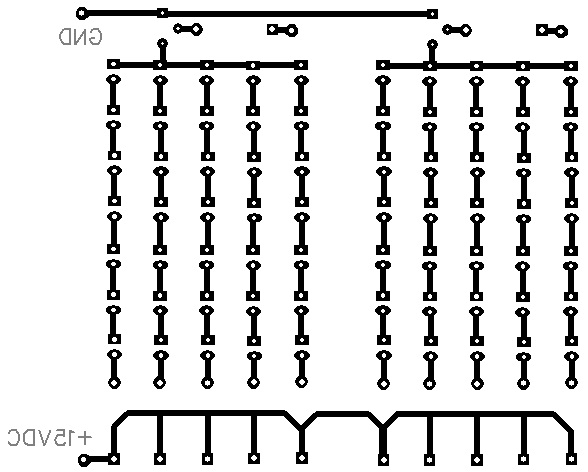
If you ever look at an electronics store there led running with structured into these words by which I mean the circuit board using the name goes with LEDs. The circuit is very simple not to use a computer program using only pure manual SN 74 164 digital IC and passive components other support you are able to be creative with these electronic circuits.
This circuit has the same principles as the previous series, which led a simple walk 7 (seven) canal. This circuit is complete with two (2) pieces of IC 74 164 at once so as to produce 15 canal. This then led Canal connected in such a way (series-parallel) so as to form a particular article as we want.
For
the circuit can be seen from the picture below, the circuit board
running the name is still the manual model has not been using dot matrix
or running text that use a specific code for the fed to ICnya. Preparation of a form letter that led to such an extent that is essential to note. So that led woven into the letters will be a post so this circuit is called a series nameplate walk.Things that need to be considered before Making Networks Board Names walk from the LED array
Use regular LEDs do not clear.
Paint the top of the PCB with a dark color (black).
Note the LED specifications. In this experiment using ordinary LED red, specification voltage of 3 volts.
How to install and set LED:
One letter composed at most 5 columns and 7 rows.
One column at most composed by 6 LEDs diseri.
Then the fifth column linked in parallel.
Each column is given a bottleneck, Rx, which depends on the number of LEDs in one column and depends also on the type of LED.
In the column consisting of 6 LEDs, Rx = 330 ohm; 5 LED, Rx = 560 ohm; 4 LEDs, Rx = 680 ohm
Remember, you should be able to test if the other colors.
Each letter was given FCS9013 transistor amplifier.
Here is a scheme of the letters LED.

Medium picture below is lay out on nameplate 2 letter. To create a nameplate 8 letter, copied from the second stay this letter.
Here is lay out underneath.
Here is lay out underneath.
Examples of arrangement of LEDs on the letters A and B:

Rx value in the first column and the fifth (the letter A) amounted to 560 ohms, because it consists of five LEDs arranged series. Rx in the second column, third, and fourth, of 680 ohms because it consists of 2 LED.
Rx first column letters B, 330 ohms. Rx column of the second, third, fourth, and fifth of 680 ohms.
Rx first column letters B, 330 ohms. Rx column of the second, third, fourth, and fifth of 680 ohms.


Tidak ada komentar:
Posting Komentar