

Matrix Keypad buttons are arranged in matrices (rows x columns) so as to reduce the use of the input pin. For example, a 4 × 4 matrix keypad simply use the 8-pin to 16 keys. This is possible because of a series of buttons arranged horizontally and vertically to form lines forming columns:

And I would cite as where the workings of the 4x4 keypad, for example, I will try to push the button 9 then the circuit that works like the picture below:

By knowing that the data originated from B3, and feed it over the K3 is detected, it can be concluded that the button is pressed is the "9".

application examples keypad (input) at a temperature regulator
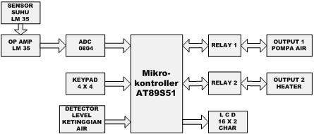
Microcontroller applications as Regulator Temperature and Altitude Water Level Indicator on the electric water heater with a view LCD (Liquid Crystal Display), composed of several separate circuits. Each circuit can be connected to the connector if want a joint application, with input and output are different.
The system can be translated into several smaller modules, which consists of five parts:
1. Minimum System Module Microcontroller AT89S51 as controller / controller
2. The temperature sensor module with IC LM35DZ as temperature sensors and Op Amp CA3140A as a signal amplifier to the ADC input 0804
3. The ADC module 0804 as an input analog to digital
4. The water sensor module with a comparator circuit LM 311
5. M1632 LCD modules as output / display.
Microcontroller processes the work done is determined by the input and output based on logic conditions from sensors that support the system, to be compared with the logic of the program in the microcontroller.
How it Works Modules
How the system works is closely related to the workings of microcontroller applications are made. To understand how the system works, it first must understand how each module, the following is an explanation of how each module: This series Minimum System Microcontroller AT89S51Pada Minimum System Microcontroller AT89S51 is not possible to use two modules inputs and three modules output are provided together at the same time, given the limitations of the microcontroller port only has four parallel port and a serial port which is a special function of one of the parallel port. Figure 3-2 is shown the minimum system microcontroller AT89S51.
How the system works is closely related to the workings of microcontroller applications are made. To understand how the system works, it first must understand how each module, the following is an explanation of how each module: This series Minimum System Microcontroller AT89S51Pada Minimum System Microcontroller AT89S51 is not possible to use two modules inputs and three modules output are provided together at the same time, given the limitations of the microcontroller port only has four parallel port and a serial port which is a special function of one of the parallel port. Figure 3-2 is shown the minimum system microcontroller AT89S51.
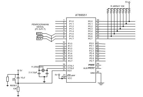
Minimum System microcontroller on the above, there are two additional circuit shown, as follows:
1. Combined pin 18 (XTAL1) and 19 (XTAL2) coupled with 2 33pF capacitor and a 12 MHz crystal oscillator which serves as the generator commutator.
2. Pin 9 (RESET) coupled with the capacitor, resistor and push button switches that can be used to reset the microcontroller, the microcontroller on the state to restore the initial conditions.
In this final project work with the system microcontroller AT89S51 ISP, the application control with the microcontroller directly on a Personal Computer. All ports on the microcontroller can be used as I / O ports, but at P1.5-P1.7 is used for programming the serial mode. Pin 29 (PSEN) and pin 30 (ALE / PROG) on a minimum system is not connected to anything because the author does not use external memory as an extra.
To enter the program into the microcontroller we need a personal computer (PC). The connection between the microcontroller to a PC through the parallel port on the PC, which is connected by a cable DB25M. The connection between the microcontroller with the PC can be seen in Figure 3-3.
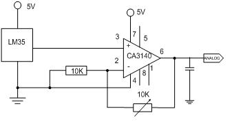
Temperature Sensor circuit (IC LM35DZ and Op Amp CA 3140A)
LM35 Temperature Sensor Module on the application of temperature gauges, used as an analog input source for the ADC module 0804. This module includes a temperature sensor IC LM35DZ that serves as a detention prisoner value variables influenced by the ambient temperature and a signal amplifier OpAmp CA3140A as entered. The characteristics of the LM35 temperature sensor are the changes in the value prisoners would be even greater if the lower temperature of their environment and little value if the prisoner will be the higher the temperature of their environment. Climate change will affect every 1ºC change in sensor output voltage of 10mV, in addition to the IC LM35 has a wide temperature range scales ranging from -55ºC to 150ºC temperature. The LM35 Temperature Sensor module circuit is shown in Figure 3-4
LM35 Temperature Sensor Module on the application of temperature gauges, used as an analog input source for the ADC module 0804. This module includes a temperature sensor IC LM35DZ that serves as a detention prisoner value variables influenced by the ambient temperature and a signal amplifier OpAmp CA3140A as entered. The characteristics of the LM35 temperature sensor are the changes in the value prisoners would be even greater if the lower temperature of their environment and little value if the prisoner will be the higher the temperature of their environment. Climate change will affect every 1ºC change in sensor output voltage of 10mV, in addition to the IC LM35 has a wide temperature range scales ranging from -55ºC to 150ºC temperature. The LM35 Temperature Sensor module circuit is shown in Figure 3-4
ADC circuit 0804
ADC module is an input module that is used to change the outer conditions in the form of analog voltages into digital data that can be processed by the system. This module uses the ADC IC 0804 which has eight input channels that can be selected. 0804 ADC IC can perform controlled conversion process, ie a process of converting the voltage change from analog to digital by the command of the microcontroller.
This ADC has a precision of one LSB, which performs voltage conversion of analog to digital by using SAR (Successive Approximation Register) with eight-bit resolution and a conversion time for 100μs. 0804 ADC module circuit is shown in Figure 3-5.
Water sensor circuit with a comparator LM 311
In the w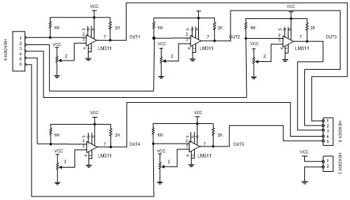 ater there is a sensor module LM comparator circuit 311 as a comparison signal enter from the condition of water levels with the conditions on program logic stored in the microcontroller AT89S51 which is then fed principle works turn to be instructions / work processes.
This module is built from the comparator circuit with IC LM 311 is an OpAmp. The way it works is this: if the voltage at the input Vin (-) = Vref (+), then switch in the LM 311 will close (to the ground) so that Vo LM 311 = 0 volts, if the condition of the input Vin (-)> Vref (+), then switch will open the on logic 1 with a voltage value Vo = 5 volts....
In the w
ater there is a sensor module LM comparator circuit 311 as a comparison signal enter from the condition of water levels with the conditions on program logic stored in the microcontroller AT89S51 which is then fed principle works turn to be instructions / work processes.This module is built from the comparator circuit with IC LM 311 is an OpAmp. The way it works is this: if the voltage at the input Vin (-) = Vref (+), then switch in the LM 311 will close (to the ground) so that Vo LM 311 = 0 volts, if the condition of the input Vin (-)> Vref (+), then switch will open the on logic 1 with a voltage value Vo = 5 volts....
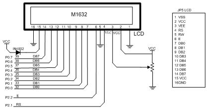
M1632 LCD circuit 16 × 2 Char.
The LCD module is an output module that is used as a display on the temperature gauge and indicator applications water levels. This module uses the M1632 LCD type which have a size of 2 × 16 characters, meaning that the LCD display is capable of displaying 16 characters in two lines of the display, so that the resulting display a number of 32 characters. The LCD module circuit is shown in Figure 3-7
The LCD module is an output module that is used as a display on the temperature gauge and indicator applications water levels. This module uses the M1632 LCD type which have a size of 2 × 16 characters, meaning that the LCD display is capable of displaying 16 characters in two lines of the display, so that the resulting display a number of 32 characters. The LCD module circuit is shown in Figure 3-7
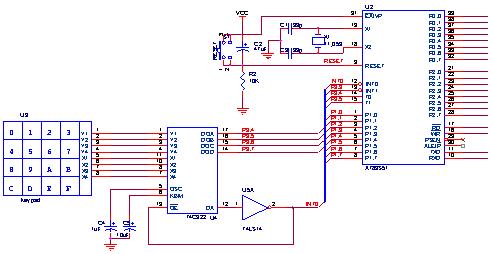
The series of 4 x 4 matrix keypad
4 × 4 keypad module is an input circuit in the form of a button that works based on the reference rows and columns. The keypad is used is 4 × 4 matrix keypad. The series of 4 × 4 matrix keypad are shown in Figure 3.9
4 × 4 keypad module is an input circuit in the form of a button that works based on the reference rows and columns. The keypad is used is 4 × 4 matrix keypad. The series of 4 × 4 matrix keypad are shown in Figure 3.9
X . I
KEYPA D THEORITY
Keypad is an essential part of an electronic device that requires human interaction. Keypad serves as an interface between a device (machine) electronics with humans or known as HMI (Human Machine Interface). 4 × 4 matrix keypad in this article is one example of a keypad that can be used to communicate between people with a microcontroller. 4 × 4 matrix keypad has a construction or arrangement that is simple and efficient in the use of the microcontroller ports. Keypad configuration with the composition of this matrix form aimed at saving microcontroller port because of the number keys (keys) required a great deal on a system with a microcontroller. Construction of 4 × 4 matrix keypad to the microcontroller can be made as shown below.

Construction Matrix Keypad 4 × 4 For Microcontroller
Construction of 4 × 4 keypad matrix above is quite simple, consisting of four rows and four columns with keypads on figure Button push switch are placed in each intersection of columns and rows. The series of the above matrix keypad consisting of 16 push switch configuration Button with 4 rows and 4 columns. 8 line consisting of four rows and four columns were connected with 8-bit microcontroller port. Side row of matrix keypad marked with the name ROW1, ROW2, Row3 and Row4 then the column marked with the name Col1, col2, col3 and col4. Input or output side of the 4 × 4 matrix keypad is not binding, can be configured as a column and line input as output or vice versa depending on programmer
Scanning Process Matrix Keypad 4 × 4 For Microcontroller
Scanning process to read keystrokes on a 4 × 4 matrix keypad to the microcontroller done gradually over a column-by-column from the first column to column 4 and the first row to row to 4. The program for scanning a 4 × 4 keypad matrix can vary, but essentially the same. Suppose we assume active keypad LOW (all the columns and rows fitted line pull-up resistor) and is connected to the port micro controller the column lines are input lines and lane line is the output line scanning process keypad matrix 4 × 4 above can be written as follows.
• Sending a logic Low to column 1 (Col1) and logic HIGH for another column and then read data lines, eg SW1 button is pressed, the data first row (ROW1) will be LOW so that the data rows read is 0111, or the button is pressed the button SW5 then data on line 2 will be LOW so that data is read 1011, or button SW9 is pressed so that the data is unreadable 1101, or switch SW13 is pressed, the data is read is 1110 and or no button on the first column in the press and then the data readout line will be in 1111.• Sending a logic Low to column 2 (col2) and logic HIGH for another column and then read data lines, eg SW1 button is pressed, the data first row (ROW1) will be LOW so that the data rows read is 0111, or the button is pressed the button SW5 then data on line 2 will be LOW so that data is read 1011, or button SW9 is pressed so that the data is unreadable in 1101, or the key SW13 is pressed, the data is read is 1110 and or no button on the first column in the press and then the data readout line will be in 1111.• Sending a logic Low to column 3 (col3) and logic HIGH for another column and then read data lines, eg SW1 button is pressed, the data first row (ROW1) will be LOW so that the data rows read is 0111, or the button is pressed the button SW5 then data on line 2 will be LOW so that data is read 1011, or button SW9 is pressed so that the data is unreadable in 1101, or the key SW13 is pressed, the data is read is 1110 and or no button on the first column in the press and then the data readout line will be in 1111.• Sending a logic Low to column 4 (col4) and logic HIGH for another column and then read data lines, eg SW1 button is pressed, the data first row (ROW1) will be LOW so that the data rows read is 0111, or the button is pressed the button SW5 then data on line 2 will be LOW so that data is read 1011, or button SW9 is pressed so that the data is unreadable 1101, or switch SW13 is pressed, the data is read is 1110 and or no button on the first column in the press and then the data readout line will be in 1111.
Then the data is processed as a line reading of the data reading keypad key presses. So that each key on the keypad matrix 4 × 4 above with the scanning technique will produce suppression of data each key are as follows.
Then the data is processed as a line reading of the data reading keypad key presses. So that each key on the keypad matrix 4 × 4 above with the scanning technique will produce suppression of data each key are as follows.
SW1 = 0111 0111 SW9 = 0111 1101
SW2 = 1011 0111 SW10 = 1011 1101
SW3 = 1101 0111 SW11 = 1101 1101
SW4 = 1110 0111 SW12 = 1110 1101
SW5 = 0111 1011 SW13 = 0111 1110
SW6 = 1011 1011 SW14 = 1011 1110
SW7 = 1101 1011 SW15 = 1101 1110
SW8 = 1110 1011 SW16 = 1110 1110
SW2 = 1011 0111 SW10 = 1011 1101
SW3 = 1101 0111 SW11 = 1101 1101
SW4 = 1110 0111 SW12 = 1110 1101
SW5 = 0111 1011 SW13 = 0111 1110
SW6 = 1011 1011 SW14 = 1011 1110
SW7 = 1101 1011 SW15 = 1101 1110
SW8 = 1110 1011 SW16 = 1110 1110
Data port microcontroller, eg in SW2 = 1011 0111 is divided into nibble above and nibble under which the data nibble on (1011) is the data that we send while data nibble under (0111) is a data readings presses keypad button SW2 on the scanning process matrix keypad 4 × 4 above.
example
X . II
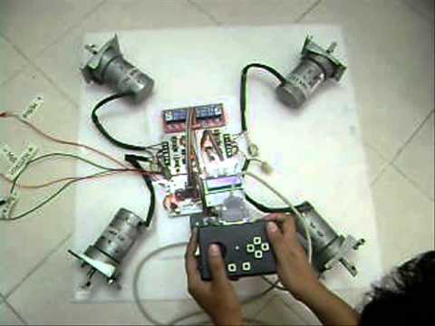
JOYSTI CK CIRCUIT
Shoot, it used to be you'd have a whole team of iRobo robos, to man your factory or diffuse your explosives, but each one required its own joystick controller. That's a lot to carry for a robo operator. But not anymore! Now iRobo has one Android app to man all its defense and security bots.

PWM DC Motor Control with Analog
Two Common Problems
DC motor control is generally composed of two issues:
1. Controlling the direction of rotary
2. Controlling the rotational speed
Setting the Directions Play
Using the manual switch to change the direction of current into DC motor. Using a mechanical switch is very easy but slow, and difficult or impossible to be connected to a controller

H-Bridge
The power transistor replaces the function of the manual switch. The transistors are arranged around a DC motor, so that in schematic form the letter H. Avoid (A and B) or (D and C) light simultaneously.
The power transistor replaces the function of the manual switch. The transistors are arranged around a DC motor, so that in schematic form the letter H. Avoid (A and B) or (D and C) light simultaneously.

Transistor vs. Switch
Very fast response transistor (order of micro-seconds). Transistors can be controlled easily by a microcontroller or another. Can use power transistors for the motor with large currents.
Can adjust the motor power by PWM.
BREAK: enable (B and C). PWM (Pulse Width Modulation)
PWM is essentially turning on (ON) and off (OFF) DC motor quickly. The key is to set how long the ON and OFF.
Duty Cycle
The ratio of ON time to the total time (total time = ON + OFF). Expressed in percent (%)

Make PWM (analog)

Setting the Directions Playback Simultaneously Playback Speed


Working Principle "Joystick"The position is converted into a voltage by a potentiometer. Large absolute di- -kan potentiometer voltage to drive the PWM (motor speed). Signs potentiometer voltage (+ / -) are used to determine the direction of rotary motors.

Robo manually using the "Joystick"
The construction of the Joystick Controlled System was wireless, and completely contained on a wooden base within the Arm Square of the Competition Floor.

performing Robotic Hair Transplant at Bernstein Medical
Tidak ada komentar:
Posting Komentar