Electronic Automatic Counter
A counter is a sequence of flip-flops that passes from one output condition to another output condition in order to respond to a state (set of input signals).
Counter is a digital device and the
output of the counter includes a predefined state based on the clock
pulse applications. The output of the counter can be used to
count the number of pulses. Generally, counters consist of a flip-flop
arrangement which can be synchronous counter or asynchronous counter. In
synchronous counter, only one clock i/p is given to all flip-flops,
whereas in asynchronous counter, the o/p of the flip flop is the clock signal from the nearby one. The applications of the microcontroller
need counting of exterior events such as exact internal time delay
generation and the frequency of the pulse trains. These events are
frequently used in digital systems & computers. Both these events
can be executed by software techniques, but software loops for counting
will not give the exact result slightly more important functions are not
done. These problems can be rectified by timers and counters in the
microcontrollers which are used as interrupts.
Xi 110 Counter and Types of Electronic Counters
What is Electronic Counter and Types of Counters
What is Counter?
A
Counter is a digital logic device in computing to store and display the
specific event continuously according to the configuration &
programming. Sequential digital logic circuit is a common type of
counter consist of single input line (Clock) and number of output lines.
The
value of output lines denote a number in binary number system (BCD =
Binary coded decimal). Mostly, the cascade connection of flip-flop
are used in these digital circuits. These instruments and devises
widley used in digital circuits as a separate ICs as well as combined as
parts in larger integrated circuits and PCBs.
What is Electronic Counter?
An
electronic counter is a single or multi function units device used to
specify a specific rate or time. A single function electronic counter is
either bidirectional or single directional while other pre programmed
counters are designed to perform multiple functions.
As
the name suggest, a single directional electronic counters count only
“Up” or “Down”, whereas bi directional electronic counters counts both
of “Up” and “Down”. These counters are more expensive and complicated in
installation as compared to mechanical counters. there are many types
of electronic counters as FOLLOW ( Maybe My Joke : Frequency Of Love Live On Woman .. ) .
Synchronous Counters
It
consists of parallel arrangement of flip-flops wherein all the
flip-flops are clocked simultaneously and in synchronization with the
clock pulses. This is the reason propagation delay is independent of the
number of flip-flops in the Synchronous counters.
These
counters are equipped with combinational logic circuit as well, to
ensure each flip-flop toggles at the right time. In synchronous
counters, output of one flip-flop is given to input of another
flip-flop.
Asynchronous or Ripple Counters
It
consists of a cascaded arrangement of flip-flops wherein clock pulse of
one flip-flop is driven by the output of its predecessor flip-flop. The
number of flip-flops used determine the modulus of the counter, wherein
the number of flip-flops depend upon the number of logic states in the
counter, before it reaches its initial state.
The
clock input is given to the first flip-flop. For a Modulo n counter,
the clock input to the nth flip-flop is determined by the (n-1)th
flip-flop output. Since clock of one flip-flop depends on the output of
the previous flip-flop, it would change its state after a certain time
delay which equals the propagation delays of both the flip-flops. For a
Modulus n counter, the nth flip-flop will change its state after a delay
of n times the propagation delay of one flip-flop.
Since
the clock information ripples through the counter, it is known as a
Ripple Counter. Also since the flip-flops do not change state in
synchronization with the input clock, these counters are also known as
Asynchronous counters.
Since
the final output would depend upon the propagation delay of each
counters, there is a limit to the clock frequency, which is given as:
Where
N is the number of flip-flops, td is propagation delay of one flip-flop
and Ts is the strobe pulse width. Note that the propagation delay
varies within different types of flip-flops.
Classification of Electronic Counters Based on Uses
Up/Down Counters:
As
the name suggests, these counters count in both ascending and
descending order, i.e. in forward as well as reverse direction. While
some counter ICs have separate clock input terminals for up and down
counting (Example IC 74192 and IC 74192), some have only one clock input terminal and a control pin to select the required functioning (Examples: IC 74190, IC 74191).
Decade Counters:
A
decade counter or a Module-10 counter goes through 10 unique output
combination states until it resets. It consists of 4 flip-flops and
requires additional circuitry to skip few states, toconvert the normal
counter to a decade counter. It can count 16 possible states, out of
which only 10 are used. Examples are 4017B, 7490N.
BCD Counter:
It is a special type of decade counter whose output is in accordance with the 8421 code. The counter states are the binary equivalent of decimal numbers. Example is 74LS90.
Presettable Counters:
These
are counters which can be pre-set to any initial count, with the help
of the PRESET and CLEAR pins of the Flip-Flops. The flip-flops can be
clocked asynchronously or synchronously. Presettable counters can be UP
counters, DOWN counters or UP/DOWN counters.
These
consist of additional input/output pins such as ‘Preset’ (To load any
desired count), Parallel Load (PL) inputs (allows PRESET inputs to be
loaded to the outputs), and Terminal Count (TC) outputs (becomes active
when terminal count is reached.). Examples are IC74190, IC4191 and IC74193.
Ring Counter:
This
counter is developed by modifying a shift register. The true output of
the last flip-flop is fed back directly to the data input of the first
flip-flop, thus generating a sequence of pulses. For example, for a D
Flip-Flop shift register, the Q output of the last flip-flop is
connected to the D input of the first flip-flop. These counters are used
in digital system to generate control pulses.
Johnson Counter
This
counter is a reverse of Ring Counter. In other words, feedback from the
last flip-flop is fed inversely to the data input of the first
flip-flop. For example, for a D Flip-Flop
shift register, the ~Q output of the last flip-flop is fed to the D
input of the first flip-flop. These can be used as Divide by n counters
as well.
Practical Counter IC 4017: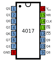
It
is a 16 pin, CMOS logic Decade Counter cum Decoder, used mainly for low
range counting applications. It can count from zero to ten, with
decoded outputs, thus saving a lot of board space and time.
Functions of the IN/OUT PINS Of Counter IC 4017
Given below is the functionality of each of its pins.
Pins 1 to 7, 9 to 11: These are output pins of the IC, with each pin going high with corresponding decimal count. The status is as given below.
Pin 1: Goes HIGH when ‘5’ is the count.
Pin 2: Goes HIGH when ‘1’ is the count.
Pin 3: Goes HIGH when ‘0’ is the count.
Pin 4: Goes HIGH on count ‘2’.
Pin 5: Goes HIGH on count ‘6’
Pin 6: Goes HIGH on count 7.
Pin 7: Goes HIGH when count is ‘3’.
Pin 8: It is the ground pin, which is connected to LOW level voltage or to the ground.
Pin 9: Goes HIGH when count is ‘8’.
Pin 10: Goes HIGH when count is ‘4’.
Pin 11: Goes HIGH when count is ‘9’.
Pin 12:
This pin is used for connecting with another Counter IC, to support
larger counting order. Though we can achieve counts to 20 or more, by
cascading multiple IC4017s together, it is advised not to cascade more than 3 ICs, in order to avoid occurrence glitches.
Pin 13:
This is an Active LOW pin and is termed as the Disable pin. Once given a
logic HIGH signal, it will disable the whole function of the IC,
irrespective of the clock pulses.
Pin 14:
This is the clock input pin. The input clock pulses are given to this
pin and the count advances on rising or positive edge of the pulse.
Pin 15: This is the Active LOW reset pin, which once given a ‘HIGH’ logic signal would reset the IC.
Pin 16: This is the Power Supply pin which should be given a voltage from 3 Volts to 15 Volts.
Applications/Uses of Counters
Electronic
counters are used in many digital electronic devices especially in
digital clock and multiplexing. Most of their applications are listed
below.
- As object counters
- Parallel to serial data conversion logic circuits
- Analog to digital convertors.
- Digital clocks
- Frequency counters
- Frequency divider circuits. (Where the Input frequency divided by 2)
- Timers and Rate measurement. (Time circuits, Washing machines, Alarm clock etc)
- Digital triangular wave generator.
- Generating staircase voltage
Types of Counters
Counters can be categorized into different types according to the way they are clocked. They are ;
- Asynchronous Counters
- Synchronous Counters
- Asynchronous Decade Counters
- Synchronous Decade Counters
- Asynchronous Up-Down Counters
- Synchronous Up-Down Counters
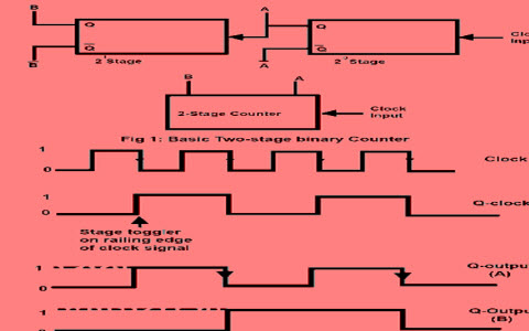
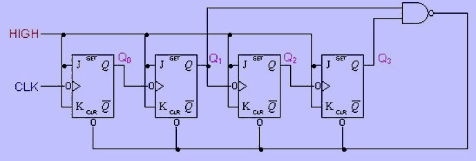
Asynchronous Counters
The diagram of a 2-bit asynchronous
counter is shown below. The exterior clock is connected to the clock i/p
of the FF0 (first flip-flop) only. So, this FF changes the state at the
decreasing edge of every clock pulse, but FF1 changes only when
activated by the decreasing edge of the Q o/p of FF0. Because of the
integral propagation delay through a FF, the change of the i/p clock
pulse and a change of the Q o/p of FF0 can never occur at precisely the
same time. So, the FF’s cannot be activated concurrently, generating an
asynchronous operation.
Note that for ease, the changes of Q0,Q1
& CLK in the above diagram are shown as concurrent, even though
this is an asynchronous counter. Actually, there is a small delay b/n
the Q0, Q1 and CLK changes.
Generally, all the CLEAR i/ps are
connected together, so before counting starts then that a single pulse
can clear all the FFs. The clock pulse fed into FF0 is rippled through
the new counters after propagation delays, such as a ripple on the
water, hence the term Ripple Counter.
The circuit diagram of the two bit
ripple counter includes four different states ,each one consisting with a
count value. Likewise, a counter with n FFs can have 2N states. The
number of states in a counter is called as its mod number. Therefore a
two-bit counter is a mod-4 counter.
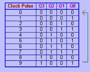
Asynchronous Decade Counters
In the previous counter have 2n states.
But, counters with states less than 2n is also possible. These are
designed to have the no. of states in their series.These are called
shortened sequences which are accomplished by driving the counter to
recycle before going through all of its states. A common modulus for
counters with shortened sequence is 10. A counter with 10-states in its
series is called a decade counter.The implemented decade counter circuit
is given below.
X
When
the counter counts to ten, then all the FFs will be cleared. Notice
that only Q1&Q3 both are used to decode the count of 10, that is
called partial decoding. At the same time one of the other states from
0-9 have both Q1&Q3 will be high. The series of the decade counter
table is given below.
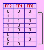
Asynchronous Up-Down Counters
In particular applications, a counter
must be capable to count both up & down. The below circuit is a
three bit up & down counter, that counts UP or DOWN based on the
control signal status. When the UP i/p is at 1 & the DOWN i/p is at
0, the NAND gate between FF0 & FF1 will gate the non-inverted o/p
(Q) of flip flop (FF0) into the clock i/p of flip flop (FF1). Likewise,
the non-inverted o/p of Flip Flop1 will be gated through the other NAND
gate into the clock i/p of flip-flop2. Therefore the counter will count
up.
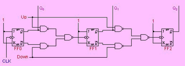
Once the control i/p (UP) is at 0 &
DOWN is at 1, the inverted o/ps of flip-flop0 (FF0) and flip-flop1 (FF)
are gated into the clock i/ps of FF1 & FF2 separately. If the FFs
are initially changed to 0’s, then the counter will go through the below
series as i/p pulses are applied. Notice that an asynchronous up-down
counter is slower than an UP counter/down counter because of an extra
propagation delay introduced by the NAND gates.
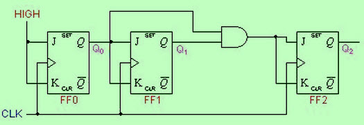
Synchronous Counters
In this type of counters,
the CLK i/ps of all the FFs are connected together and are activated by
the i/p pulses. So, all the FFs change states instantaneously. The
circuit diagram below is a three bit synchronous counter. The inputs J
and K of flip-flop0 are connected to HIGH. Flip-flop 1 has its J &K
i/ps connected to the o/p of flip-flop0 (FF0), and the inputs J & K
of flip-flop2 (FF2) are connected to the o/p of an AND gate that is fed
by the o/ps of flip-flop0 and flip-flop1. When the both the outputs of
FF0 & FF1 are HIGH. The positive edge of the fourth CLK pulse will
cause FF2 to alter its state because of the AND gate.
The series of the three bit counter
table is given below.The major advantage of these counters is that there
is no increasing time delay due to all FFs are activated in parallel.
Thus, the max operating frequency of this synchronous counter will be
considerably higher than for the equivalent ripple counter.
Synchronous Decade Counters
Synchronous counter counts from 0-9
similar to asynchronous counter and then again recycles zero. This
process is done by driving the 1010 states back to the 0000 state. This
is termed as truncated sequence, that can be designed by the below
circuit.
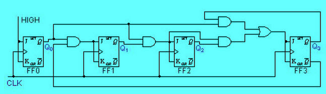
- Q0 ties on each and every CLK pulse
- Q1 alters on the next clock pulse every time when Q0=1 & Q3=0.
- Q2 alters on the next clock pulse every time when Q0=Q1=1.
- Q3 alters on the next CLK pulse each and every time when Q0=1, Q1=1 & Q2=1 (count 7), or when Q0=1 & Q3=1 (count 9).

The above characteristics are employed with the AND gate or OR gate. The logic diagram of this is shown in the above diagram.
Synchronous Up-Down Counters
A three bit synchronous Up-Down counter,
tabular form and series are given below. This type of counter has an
up-down control i/p similar to asynchronous up-down counter, that is
used to control the counter’s direction through a certain series.
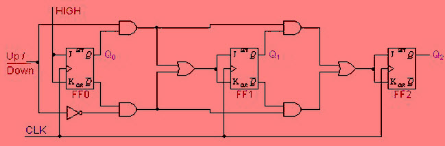
- Q0 ties on each CLK pulse for both up & down series
- When Q0=1 for the up series, then the state of the Q1 changes on the next CLK pulse.
- When Q0=0 for the down series, then the state of the Q1 changes on the next CLK pulse.
- When Q0=Q1=1 for the up series, then the state of the Q2 changes on the next CLK pulse.
- When Q0=Q1=0 for the down series, then the state of the Q2 changes on the next CLK pulse.
X
The
above characteristics are employed with the AND gate, OR gate and NOT
gate. The logic diagram of this is shown in the above diagram.
Applications of Counters
The applications of the counters mainly
involve in digital clocks and in multiplexing. The best example of the
counter is parallel to serial data conversion logic discussed below.
A set of bits, performing concurrently
on parallel lines is called parallel data. A set of bits, performing on a
single line in a time series is called serial data. The
Parallel-to-serial data conversion is normally is done by using a
counter to afford a binary series of the data, select i/ps of a MUX, as
explained in the circuit below.
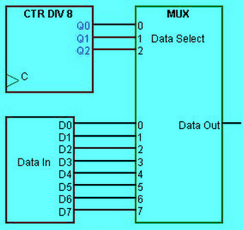
In the above circuit, modulo-8 counter consist of Q o/ps, that are connected to the data, select i/ps of an 8-bit MUX.
The first 8-bit group of parallel data is applied to the inputs of the
MUX. As the counter goes through a binary series from 0-7, each bit
starts with D0, is serially selected & passed through the MUX to the
o/p line. After 8-CLK pulses, the data byte has been changed to a
serial format & sent out through the transmission line. Then, the
counter reprocesses back to 0 and changes another parallel byte serially
again in the similar process.
Timers and Counters in 8051 Microcontroller and its Applications
Many of the microcontroller applications
require counting of external events such as frequency of the pulse
trains and generation of precise internal time delays between computer
actions. Both these tasks can be implemented by software techniques, but
software loops for counting, and timing will not give the exact result
rather more important functions are not done. To avoid these problems,
timers and counters in the micro-controllers are better options for
simple and low-cost applications. These timers and counters are used as interrupts in 8051 microcontroller.
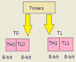
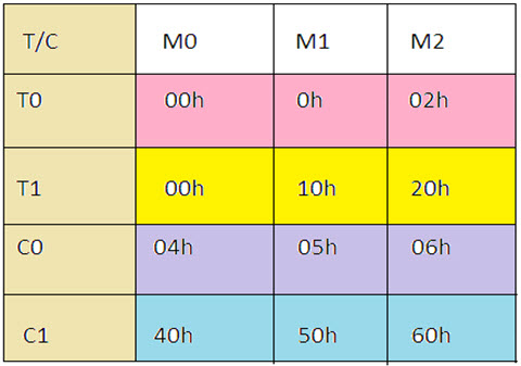
There are two 16-bit timers and counters in 8051 microcontroller:
timer 0 and timer 1. Both timers consist of 16-bit register in which
the lower byte is stored in TL and the higher byte is stored in TH.
Timer can be used as a counter as well as for timing operation that
depends on the source of clock pulses to counters.
Counters and Timers in 8051
microcontroller contain two special function registers: TMOD (Timer Mode
Register) and TCON (Timer Control Register), which are used for
activating and configuring timers and counters.
Timer Mode Control (TMOD):
TMOD is an 8-bit register used for selecting timer or counter and mode
of timers. Lower 4-bits are used for control operation of timer 0 or
counter0, and remaining 4-bits are used for control operation of timer1
or counter1.This register is present in SFR register, the address for
SFR register is 89th.
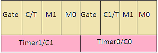
C/T: If the C/T bit is ‘1’, then it is acting as a counter mode, and similarly when set C+
=/T bit is ‘0’; it is acting as a timer mode.
=/T bit is ‘0’; it is acting as a timer mode.
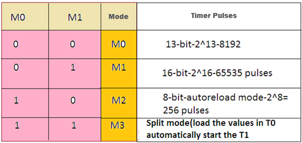
Mode select bits: The M1 and M0 are mode select bits, which are used to select the timer operations. There are four modes to operate the timers.
Mode 0: This is a 13-bit mode that means the timer operation completes with “8192” pulses.
Mode 1: This is a16-bit mode, which means the timer operation completes with maximum clock pulses that “65535”.
Mode 2: This mode is an 8-bit auto reload mode, which means the timer operation completes with only “256” clock pulses.
Mode 3: This mode is a split-timer mode, which means the loading values in T0 and automatically starts the T1.
Mode selection Values of timers and counter in 8051
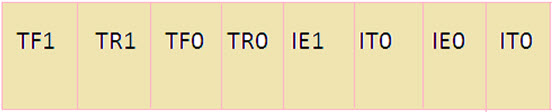
EX: while (TF1==1)
Whenever the TF1=1, then clear the flag bit and stop the timer.
TR1: The TR1 stands for
timer1 start or stop bit. This timer starting can be through software
instruction or through hardware method.
EX: gate=0 (start timer 1 through software instruction)
TR1=1; (Start timer)
TR1=1; (Start timer)
TF0: The TF0 stands for
‘timer0’ flag-bit. Whenever calculating the time delay in timer1, the
TH0 and TL0 reaches to a maximum value that is ‘FFFF’, automatically.
X
EX: while (TF0==1)
Whenever the TF0=1, then clear the flag bit and stop the timer.
Whenever the TF0=1, then clear the flag bit and stop the timer.
TR0: The TR0 stands for
‘timer0’ start or stop bit; this timer starting can be through software
instruction or through hardware method.
EX: gate=0 (start timer 1 through software instruction)
TR0=1; (Start timer)
TR0=1; (Start timer)
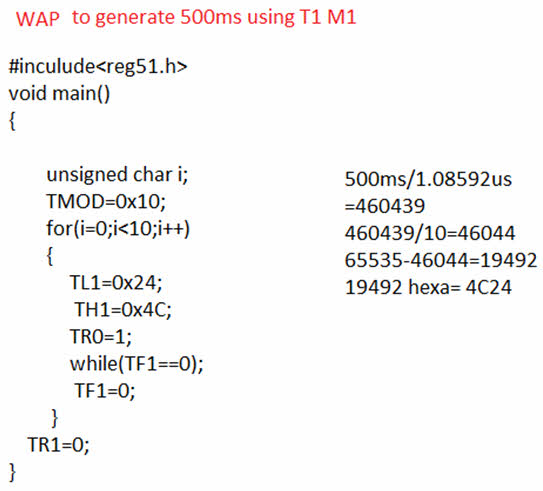
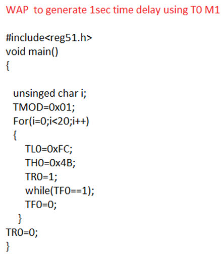
Time Delay Calculations for 8051 Microcontroller
The 8051 microcontroller works with 11.0592 MHz frequency.
Frequency 11.0592MHz=12 pules
1 clock pulse =11.0592MHz/12
F =0.921 MHz
Time delay=1/F
T=1/0.92MHz
T=1.080506 us (for ‘1’ cycle)
X
1000us=1MS
1000ms=1sec
Procedure to Calculate the Delay Program
1. First we have to load the TMOD
register value for ‘Timer0’ and ‘Timer1’in different modes. For example,
if we want to operate timer1 in mode1 it must be configured as
“TMOD=0x10”.
2. Whenever we operate the timer in mode
1, timer takes the maximum pulses of 65535. Then the calculated
time-delay pulses must be subtracted from the maximum pulses, and
afterwards converted to hexadecimal value. This value has to be loaded
in timer1 higher bit and lower bits. This timer operation is programmed
using embedded C in a microcontroller.
Example: 500us time delay
500us/1.080806us
461pulses
P=65535-461
P=65074
65074 conveted by hexa decimal =FE32
X
TH1=0xFE;
TL1=0x32;
3. Start the timer1 “TR1=1;”
4. Monitor the flag bit “while(TF1==1)”
5. Clear the flag bit “TF1=0”
6. Cleat the timer “TR1=0”
Example Programs:
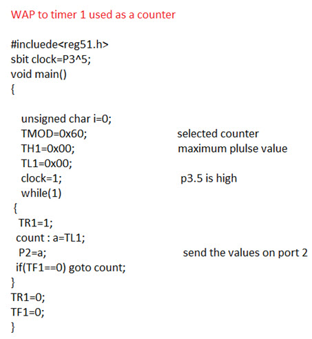
Counters in 8051
We can use a counter by keeping C/T bit
high, i.e., logic ‘1’ in the TMOD register. For better understanding, we
have given one program which uses timer 1 as a counter. Here the LEDs
are connected to 8051 Port 2, and the switch to the timer1 pin P3.5; and
therefore, if the switch is pressed, the value will be counted.
Otherwise, an externally connected sensor to this counter pin as input
does this counting operation.
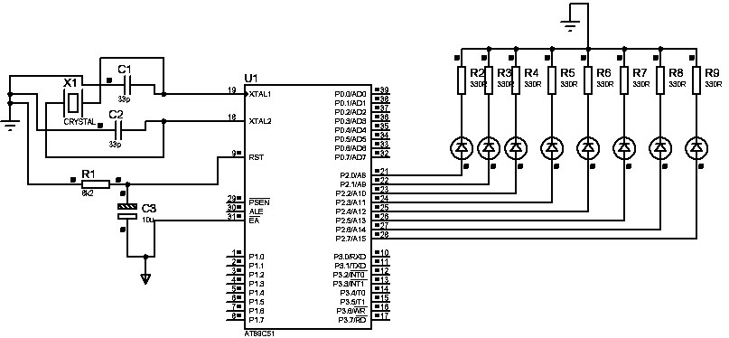
Applications of Timers and Counters in 8051
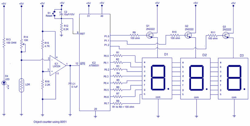
Digital Counter with 8051
The Digital counter with 8051 is
achieved by programming the microcontroller as discussed above and by
attaching a sensor system to it. This object counter uses IR sensor that detects the obstacle near to it and also enables the pin of the microcontroller
06. When an object passes through the sensors, then the microcontroller
gets an interrupt signal from the IR sensors and increment the count
which is displayed in the7-segment display.
Time delay circuit Using 8051 microcontroller
The below figure shows how the timer
operation can be implemented for switching the LEDs in an effective way.
The time delay operation for the set of LEDs is programmed in a
microcontroller in the manner discussed above. Here, a set of LEDs are
connected to the port 2 with a common supply system. When this circuit
is turned on based on the time delay program in the microcontroller appropriately, these LEDs are switched on.

Counters in Digital Logic
According to electronic book , in digital logic and computing, a Counter
is a device which stores (and sometimes displays) the number of times a
particular event or process has occurred, often in relationship to a
clock signal. Counters are used in digital electronics for counting
purpose, they can count specific event happening in the circuit. For
example, in UP counter a counter increases count for every rising edge
of clock. Not only counting, a counter can follow the certain sequence
based on our design like any random sequence 0,1,3,2… .They can also be
designed with the help of flip flops.
Counter Classification
- Asynchronous counter
- Synchronous counter
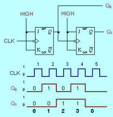
In asynchronous counter we don’t use universal clock, only first flip flop is driven by main clock and the clock input of rest of the following counters is driven by output of previous flip flops. We can understand it by following diagram-
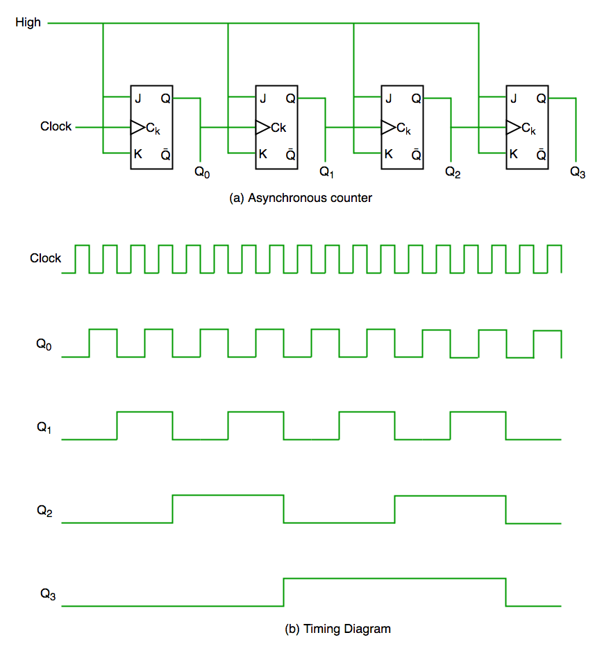
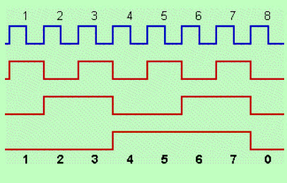
It is evident from timing diagram that Q0 is changing as soon as the rising edge of clock pulse is encountered, Q1 is changing when rising edge of Q0 is encountered(because Q0 is like clock pulse for second flip flop) and so on. In this way ripples are generated through Q0,Q1,Q2,Q3 hence it is also called RIPPLE counter.
2. Synchronous Counter
Unlike the asynchronous counter, synchronous counter has one global clock which drives each flip flop so output changes in parallel. The one advantage of synchronous counter over asynchronous counter is, it can operate on higher frequency than asynchronous counter as it does not have cumulative delay because of same clock is given to each flip flop.
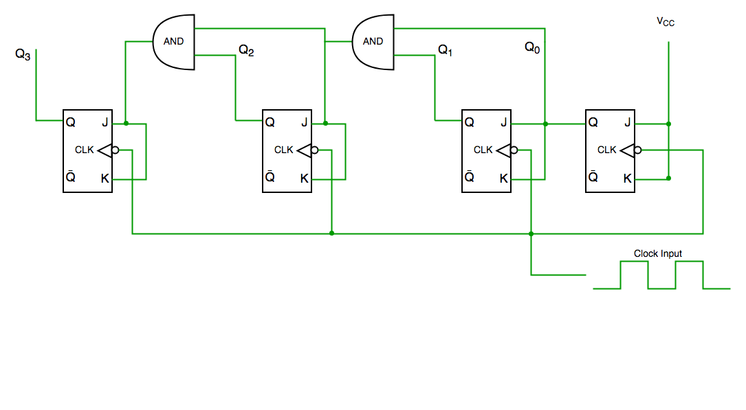
Synchronous counter circuit

Timing diagram synchronous counter
From circuit diagram we see that Q0 bit gives response to each
falling edge of clock while Q1 is dependent on Q0, Q2 is dependent on Q1
and Q0 , Q3 is dependent on Q2,Q1 and Q0.
Decade Counter
A decade counter counts ten different states and then reset to its
initial states. A simple decade counter will count from 0 to 9 but we
can also make the decade counters which can go through any ten states
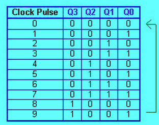
between 0 to 15(for 4 bit counter).| Clock pulse | Q3 | Q2 | Q1 | Q0 |
| 0 | 0 | 0 | 0 | 0 |
| 1 | 0 | 0 | 0 | 1 |
| 2 | 0 | 0 | 1 | 0 |
| 3 | 0 | 0 | 1 | 1 |
| 4 | 0 | 1 | 0 | 0 |
| 5 | 0 | 1 | 0 | 1 |
| 6 | 0 | 1 | 1 | 0 |
| 7 | 0 | 1 | 1 | 1 |
| 8 | 1 | 0 | 0 | 0 |
| 9 | 1 | 0 | 0 | 1 |
| 10 | 0 | 0 | 0 | 0 |
Truth table for simple decade counter
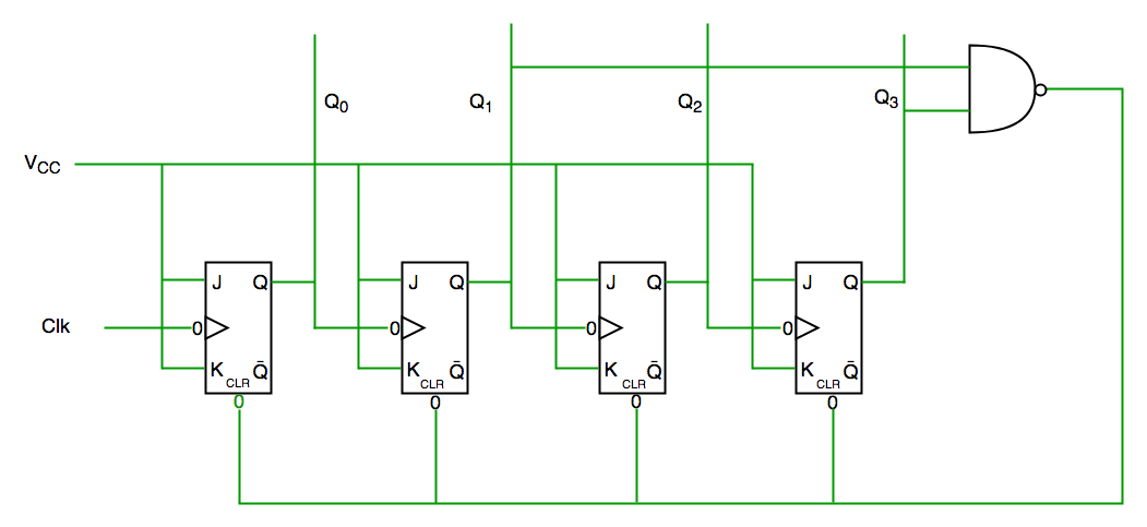
Decade counter circuit diagram
We see from circuit diagram that we have used nand gate for Q3 and Q1
and feeding this to clear input line because binary representation of
10 is—1010
And we see Q3 and Q1 are 1 here, if we give NAND of these two bits to clear input then counter will be clear at 10 and again start from beginning.
Important point: Number of flip flops used in counter are always greater than equal to (log2 n) where n=number of states in counter.
Some previous years gate questions on Counters
Q1. Consider the partial implementation of a 2-bitt counter using T flip-flops following the sequence 0-2-3-1-0, as shown below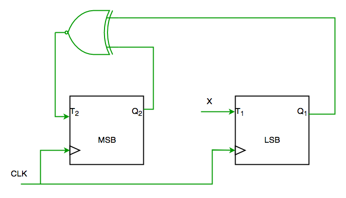
To complete the circuit, the input X should be
(A) Q2′
(B) Q2 + Q1
(C) (Q1 ⊕ Q2)’
(D) Q1 ⊕ Q2 (GATE-CS-2004)
Solution:
From circuit we see
T1=XQ1’+X’Q1—-(1)
AND
T2=(Q2 ⊕ Q1)’—-(2)
AND DESIRED OUTPUT IS 00->10->11->01->00
SO X SHOULD BE Q1Q2’+Q1’Q2 SATISFYING 1 AND 2.
SO ANS IS (D) PART.
Q2. The control signal functions of a 4-bit binary counter are given below (where X is “don’t care”)
The counter is connected as follows:
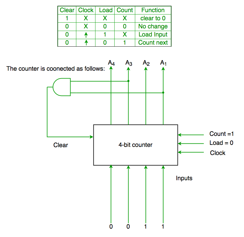
Assume that the counter and gate delays are negligible. If the counter starts at 0, then it cycles through the following sequence:
(A) 0,3,4
(B) 0,3,4,5
(C) 0,1,2,3,4
(D) 0,1,2,3,4,5 (GATE-CS-2007)
Solution:
Initially A1 A2 A3 A4 =0000
Clr=A1 and A3
So when A1 and A3 both are 1 it again goes to 0000
Hence 0000(init.) -> 0001(A1 and A3=0)->0010 (A1 and A3=0) -> 0011(A1 and A3=0) -> 0100 (A1 and A3=1)[ clear condition satisfied] ->0000(init.) so it goes through 0->1->2->3->4
Ans is (C) part.


SPACESHIPS INTERIOR
Digital counters
An
electronic counter is a sequential digital device, which is used for
counting the number of pulses that are coming at the input line in a
certain time period. There are many different types of counters. The
simplest type of digital counters track and count time and work
similarly as a well-known stopwatch. This means that they can be reset
and can count up to the certain value of digits.
Basic event counting

Frequency / super-counter


Frequency/super-counter mode has many advantages over traditional counter measurements.
The problem with traditional counters is that the value of the counter is latched only at a sample rate interval. Therefore, we only have discrete values on each sample. Since the counters can measure exactly where the position of the pulse is between two samples, we can calculate two things out of this: the exact interpolated position of the counter at the sample point, as well as the exact frequency of the pulses.
Space Fighter

Xi 110 110 Electronic countermeasure
An electronic countermeasure (ECM) is an electrical or electronic device designed to trick or deceive radar, sonar or other detection systems, like infrared (IR) or lasers. It may be used both offensively and defensively to deny targeting information to an enemy. The system may make many separate targets appear to the enemy, or make the real target appear to disappear or move about randomly. It is used effectively to protect aircraft from guided missiles. Most air forces use ECM to protect their aircraft from attack. It has also been deployed by military ships and recently on some advanced tanks to fool laser/IR guided missiles. It is frequently coupled with stealth advances so that the ECM systems have an easier job. Offensive ECM often takes the form of jamming. Self-protecting (defensive) ECM includes using blip enhancement and jamming of missile terminal homers.
Inspecting an Electronic Attack Pod.
The first example of electronic countermeasures being applied in a combat situation took place during the Russo-Japanese war. On April 15, 1904, Russian wireless telegraphy stations installed in the Port Arthur fortress and on board Russian light cruisers successfully interrupted wireless communication between a group of Japanese battleships. The spark-gap transmitters in the Russian stations generated senseless noise while the Japanese were making attempts to coordinate their efforts in the bombing of a Russian naval base. Germany and United Kingdom interfered with enemy communications along the western front during World War I while the Royal Navy tried to intercept German naval radio transmissions. There were also efforts at sending false radio signals, having shore stations send transmissions using ships' call signs, and jamming enemy radio signals.
World War II ECM expanded to include dropping chaff (originally called Window), jamming and spoofing radar and navigation signals. German bomber aircraft navigated using radio signals transmitted from ground stations, which the British disrupted with spoofed signals in the Battle of the Beams. During the RAF's night attacks on Germany the extent of electronic countermeasures was much expanded, and a specialised organisation, No. 100 Group RAF, was formed to counter the increasing German night fighter force and radar defences. Cold War developments included anti-radiation missiles designed to home in on enemy radar transmitters.
In the 2007 Operation Orchard Israeli attack on a suspected Syrian nuclear weapons site, the Israel Air Force used electronic warfare to take control of Syrian airspace prior to the attack. Israeli electronic warfare (EW) systems took over Syria’s air defense systems, feeding them a false sky-picture while Israel Air Force jets crossed much of Syria, bombed their targets and returned.
Radar ECM
Basic radar ECM strategies are (1) radar interference, (2) target modifications, and (3) changing the electrical properties of air. Interference techniques include jamming and deception. Jamming is accomplished by a friendly platform transmitting signals on the radar frequency to produce a noise level sufficient to hide echos. The jammer's continuous transmissions will provide a clear direction to the enemy radar, but no range information. Deception may use a transponder to mimic the radar echo with a delay to indicate incorrect range. Transponders may alternatively increase return echo strength to make a small decoy appear to be a larger target. Target modifications include radar absorbing coatings and modifications of the surface shape to either "stealth" a high-value target or enhance reflections from a decoy. Dispersal of small aluminium strips called chaff is a common method of changing the electromagnetic properties of air to provide confusing radar echos.Communications ECM
Radio jamming or communications jamming is the deliberate transmission of radio signals that disrupt communications by decreasing the signal-to-noise ratio to the point where the target communications link is either degraded or denied service.Aircraft ECM

Fighter planes using a conventional electronically scanned antenna mount dedicated jamming pods instead or, in the case of the US, German, and Italian air forces, may rely on electronic warfare aircraft to carry them. ECM pods vary widely in power and capability; while many fighter aircraft are capable of carrying an ECM pod, these pods are generally less powerful, capable and of shorter range than the equipment carried by dedicated ECM aircraft, thus making them an important part of the inventory.
Future airborne jammers
The Next Generation Jammer is being developed to replace the current AN/ALQ-99 carried on the E/A-18G and EA-6B electronic warfare planes. Planned for adoption around 2020, it will use a small AESA antenna divided into quadrants for all around coverage and retain the capability of highly directional jamming.DARPA's Precision Electronic Warfare (PREW) project aims to develop a low-cost system capable of synchronizing several simple airborne jamming pods with enough precision to replicate the directionality of an electronically scanned antenna, avoiding collateral jamming of non-targeted receivers.
An expendable active decoy that uses DRFM technology to jam RF based threats has already been developed by Selex ES (merged into Leonardo new name of Finmeccanica since 2017). The system, named BriteCloud, is self-contained within a small canister that is similar to a standard flare cartridge. The 55 mm format of the system has undergone flight trials with the Gripen aircraft and the development of a 218 variant is at an advanced stage.
Dedicated ECM aircraft
- EC-130H Compass Call
- EA-6B Prowler equipped with ALQ-92 communications jammer, ALQ-100 multi-band track breaking system, and five ALQ-99 tactical jammer pods.
- EA-18G Growler
- EF-111A Raven
- Tornado ECR
- Su-24MP
- Yak-28PP
- Mi-8PP
- EB-66B Destroyer
Shipboard ECM
The ULQ-6 deception transmitter was one of the earlier shipboard ECM installations. The Raytheon SLQ-32 shipboard ECM package came in three versions providing warning, identification and bearing information about radar-guided cruise missiles. The SLQ-32 V3 included quick reaction electronic countermeasures for cruisers and large amphibious ships and auxiliaries in addition to the RBOC (Rapid Blooming Off-board Chaff) launchers found on most surface ships. The BLR-14 Submarine Acoustic Warfare System (or SAWS) provides an integrated receiver, processor, display, and countermeasures launch system for submarines.Infrared and acoustic analogies

BAE Hot Brick infrared jammer
Infrared and acoustic analogies
BAE Hot Brick infrared jammer
Xi 110 110 110 Let's Talk Technology

Of course, once our ships maneuver towards those unguarded orbits, they will be easily observed – and potentially countered
First ; A major development in propulsion technology, combat spacecraft would likely get around the same way the Apollo spacecraft went to the Moon and back: with orbit changes effected by discrete main-engine burns. The only other major option is a propulsion system like ion engines or solar sails, which produce a very low amount of thrust over a very long time. However, the greater speed from burning a chemical, nuclear, or antimatter rocket in a single maneuver is likely a better tactical option. One implication of rocket propulsion is that there will be relatively long periods during which Newtonian physics govern the motions of dog fighting spacecraft, punctuated by relatively short periods of maneuvering. Another is that combat in orbit would be very different from combat in "deep space," which is what you probably think of as how space combat should be – where a spacecraft thrusts one way, and then keeps going that way forever. No, around a planet, the tactical advantage in a battle would be determined by orbit dynamics: which ship is in a lower (and faster) orbit than which; who has a circular orbit and who has gone for an ellipse; relative rendezvous trajectories that look like winding spirals rather than straight lines.
Second, there are only a few ways to maneuver the attitude of a spacecraft around – to point it in a new direction. The fast ways to do that are to fire an off-center thruster or to tilt a gyroscope around to generate a torque. Attitude maneuvers would be critical to point the main engine of a space fighter to set up for a burn, or to point the weapons systems at an enemy. Either way, concealing the attitude maneuvers of the space fighter would be important to gain a tactical advantage. So We think gyroscopes ("CMGs," in the spacecraft lingo) would be a better way to go – they could invisibly live entirely within the space fighter hull, and wouldn't need to be mounted on any long booms (which would increase the radar, visible, and physical cross-section of the fighter) to get the most torque on the craft. With some big CMGs, a spacecraft could flip end-for-end in a matter of seconds or less. If you come upon a starfighter with some big, spherical bulbs near the midsection, they are probably whopping big CMGs and the thing will be able to point its guns at you wherever you go. To mitigate some of the directionality of things like weapons fire and thruster burns, space fighters would probably have weapons and engines mounted at various points around their hull; but a culture interested in efficiently mass-producing space warships would probably be concerned about manufacturing so many precision parts for a relatively fragile vessel, and the craft would likely only have one main engine rather than, say, four equal tetrahedral engines.
Nanotechnology in Space
Nanotechnology
will play an important role in future space missions. Nanosensors,
dramatically improved high-performance materials, or highly efficient
propulsion systems are but a few examples.
Propulsion systems
Most of today's rocket engines rely on chemical
propulsion. All current spacecraft use some form of chemical rocket for
launch and most use them for attitude control as well (the control of
the angular position and rotation of the spacecraft, either relative to
the object that it is orbiting, or relative to the celestial sphere).
Real rocket scientists though are actively researching new forms of
space propulsion systems.
One heavily researched area is electric
propulsion (EP) that includes field emission electric propulsion (FEEP),
colloid thrusters and other versions of field emission thrusters
(FETs). EP systems significantly reduce the required propellant mass
compared to conventional chemical rockets, allowing to increase the
payload capacity or decrease the launch mass. EP has been successfully
demonstrated as primary propulsion systems for NASA’s Deep Space 1,
Japan’s HAYABUSA, and ESA’s SMART-1 missions.
A nanotechnology EP concept
proposes to utilize electrostatically charged and accelerated
nanoparticles as propellant. Millions of micron-sized nanoparticle
thrusters would fit on one square centimeter, allowing the fabrication
of highly scalable thruster arrays.
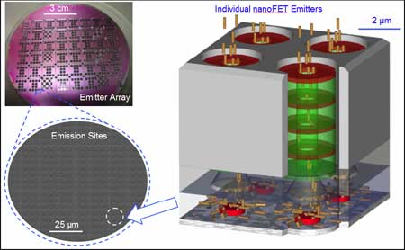
nanoFET characteristic size scales (Image: University of Michigan Department of Aerospace Engineering)
Pretty far out are proposals that the
manipulation of Casimir forces could lead to a propulsion system for
interstellar spaceships. The basic idea is that if one could exploit the
fact that vacuum is an energy reservoir, thanks to zero-point energy,
future space travelers would have access to a limitless energy source.
The only thing they need, of course, is some kind of propulsion system
that harvests the required energy from the vacuum. That this is not
totally crazy was demonstrated in a 1984 paper. Serious research efforts
are being made in various laboratories to harness the Casimir and
related effects for vacuum energy conversion
Radiation shielding
Radiation shielding is an area where
nanotechnology could make a major contribution to human space flight.
NASA says that the risks of exposure to space radiation are the most
significant factor limiting humans’ ability to participate in
long-duration space missions. A lot of research therefore focuses on
developing countermeasures to protect astronauts from those risks. To
meet the needs for radiation protection as well as other requirements
such as low weight and structural stability, spacecraft designers are
looking for materials that help them develop multifunctional spacecraft
hulls.
Advanced nanomaterials such as the newly developed, isotopically enriched boron nanotubes could pave the path to future spacecraft with nanosensor-integrated hulls that provide effective radiation shielding as well as energy storage.
Another area of required radiation shielding is
the protection of onboard electronics. It has been reported previously
that electronic devices became more radiation tolerant when their
dimensions are reduced. For example, multi-quantum well or quantum dot
devices can be tens or hundreds times more radiation tolerant than
conventional bulk devices. It even was shown that quantum dot/CNT-based
photovoltaic devices were five orders of magnitude more resistant than
conventional bulk solar cells.
Recently, a few studies on radiation effects of high energetic particles such as proton, electron, and
heavy ions on nanomaterials like carbon
nanotubes and nanowires have focused on the changed structural
properties of the nanomaterials after irradiation
Anti-satellite weapon countermeasure
In January 2007, China successfully tested an
Anti-satellite (ASAT) missile system by destroying their own defunct LEO
satellite, which generated huge amounts of space debris. This ASAT test
raised worldwide concerns about the vulnerability of satellites and
other space assets and possibility of triggering an arms race in space.
In order to meet emerging challenges posed by
such ASAT missile systems, military strategists and researchers are
developing novel technologies to protect their space assets. In view of
this, Raytheon Company has developed a counter measure system using quantum dots
to protect space assets such as satellites from missile attacks. They
have developed a decoy consisting of quantum dots of different sizes and
shapes that are engineered to emit radiation having a radiation profile
similar to that of the asset.
Space elevator
Tie a rock to the end of a piece of ribbon, then
spin it over your head. It will be pulled taut as the rock circles
about. Now, imagine a ribbon 62,000 miles long, anchored near the
equator with a weight on the other end. The centrifugal force of the
earth's rotation will make it behave the same way. You'll end up with
not only the world's biggest nunchuck, but also a kind of elevator to
outer space.
A recent research paper published at the Center for Strategy and Technology, at the Air Force's Air War College, discusses how nanotechnology can be used to improve the design of satellites
to mitigate the threats posed by ground-based directed energy weapons
and high-powered microwaves. The paper states that several nations,
including the U.S., Russia and China, already have either built or are
developing the technology to construct ground-based directed energy
weapons.
Space instrumentation
Black is black, right? Not so, according to a team of NASA engineers now developing a blacker-than pitch nanomaterial
that will help scientists gather hard-to-obtain scientific measurements
or observe currently unseen astronomical objects, like Earth-sized
planets in orbit around other stars.
The nanomaterial being developed by a team of 10
technologists at the NASA Goddard Space Flight Center in Greenbelt, Md.,
is a thin coating of multi-walled carbon nanotubes. While carbon
nanotubes would find use in the Space Elevator thanks to their
extraordinary strength, in this application, NASA is interested in using
the technology to help suppress errant light that has a funny way of
ricocheting off instrument components and contaminating measurements.
MIT hosts the Space Nanotechnology Laboratory
whose primary mission is to develop nano-fabrication, advanced
lithography and precision engineering technology for building high
performance space instrumentation, including x-ray telescopes and high
resolution x-ray spectrometers, magnetospheric imagers and solar physics
instrumentation.
What is space flight transportation?
Point-to-point is a category of sub-orbital spaceflight in which a spacecraft provides rapid transport between two terrestrial locations. Consider a conventional airline route between London and Sydney, a flight that normally lasts over twenty hours.
What is the difference between rocket and spaceship?
Rocket is a vehicle that is propelled off the Earth's surface to a certain target, space or another place on Earth. Spacecraft on the other hand is a vehicle that is used to travel in space. A rocket is used to carry the spacecraft into space. ... ISS is a spacecraft.
What are payloads in space?
Depending on the nature of the flight or mission, the payload
of a vehicle may include cargo, passengers, flight crew, munitions,
scientific instruments or experiments, or other equipment. ... For a
rocket, the payload can be a satellite, space probe, or spacecraft carrying humans, animals, or cargo.
Could humans travel at the speed of light?
The speed of light in a vacuum is 186,282 miles per second (299,792 kilometers per second), and in theory nothing can travel faster than light. In miles per hour, light speed is, well, a lot: about 670,616,629 mph. If you could travel at the speed of light, you could go around the Earth 7.5 times in one second
Will humans ever travel at the speed of light?
Einstein said it is impossible, but as Jennifer Ouellette explains some scientists are still trying to break the cosmic speed limit – even if it means bending the laws of physics. "It is impossible to travel faster than light, and certainly not desirable, as one's hat keeps blowing off."
What is a spaceship used for?
A spacecraft is a vehicle or machine designed to fly in outer space. Spacecraft are used for
a variety of purposes, including communications, Earth observation,
meteorology, navigation, space colonization, planetary exploration, and
transportation of humans and cargo.
How long does it take to get to Mars?
The trip takes
around seven months; a bit longer than astronauts currently stay on the
International Space Station. The precise duration of each journey
depends on when it is taken. Because both Mars and Earth's orbits are not perfectly circular, the time it takes to travel between them varies from six to eight months.
Can we travel back in time?
In all time travel theories allowed by real science, there is no way a traveler can go back in time to before the time machine was built. Actually, scientists and engineers who plan and operate some space missions must account for the time distortions that occur because of both General and Special Relativity.
Will humans ever travel to other galaxies?
According
to the current understanding of physics, an object within space-time
cannot exceed the speed of light, which means an attempt to travel to any other galaxy would be a journey of millions of earth years via conventional flight.
A spacecraft is a vehicle or machine designed to fly in outer space. A type of artificial satellite, spacecraft are used for a variety of purposes, including communications, Earth observation, meteorology, navigation, space colonization, planetary exploration, and transportation of humans and cargo. All spacecraft except single-stage-to-orbit vehicles cannot get into space on their own, and require a launch vehicle (carrier rocket).
On a sub-orbital spaceflight, a space vehicle enters space and then returns to the surface, without having gained sufficient energy or velocity to make a full orbit of the Earth. For orbital spaceflights, spacecraft enter closed orbits around the Earth or around other celestial bodies. Spacecraft used for human spaceflight carry people on board as crew or passengers from start or on orbit (space stations) only, whereas those used for robotic space missions operate either autonomously or telerobotically. Robotic spacecraft used to support scientific research are space probes. Robotic spacecraft that remain in orbit around a planetary body are artificial satellites. To date, only a handful of interstellar probes, such as Pioneer 10 and 11, Voyager 1 and 2, and New Horizons, are on trajectories that leave the Solar System.
Orbital spacecraft may be recoverable or not. Most are not. Recoverable spacecraft may be subdivided by method of reentry to Earth into non-winged space capsules and winged spaceplanes.
Humanity has achieved space flight but only a few nations have the technology for orbital launches: Russia (RSA or "Roscosmos"), the United States (NASA), the member states of the European Space Agency (ESA), Japan (JAXA), China (CNSA), India (ISRO), Taiwan (National Chung-Shan Institute of Science and Technology, Taiwan National Space Organization (NSPO),[7][8][9] Israel (ISA), Iran (ISA), and North Korea (NADA).

Except for the Space Shuttle, all of the recoverable crewed orbital spacecraft were space capsules.
- Crewed space capsules
 American Mercury, Gemini, and Apollo spacecraft
 Soviet Voskhod (variant of Vostok)
 1967 Soviet/Russian Soyuz spacecraft
 Chinese Shenzhou
 Line drawing of Vostok capsule


_drawing.svg)


Hubble Space Telescope

Spaceflight
Spaceflight (or space flight) is ballistic flight into or through outer space. Spaceflight can occur with spacecraft with or without humans on board.
spaceflight include space probes that leave Earth orbit, as well as satellites in orbit around Earth, such as communications satellites. These operate either by telerobotic control or are fully autonomous.Spaceflight is used in space exploration, and also in commercial activities like space tourism and satellite telecommunications. Additional non-commercial uses of spaceflight include space observatories, reconnaissance satellites and other Earth observation satellites.
A spaceflight typically begins with a rocket launch, which provides the initial thrust to overcome the force of gravity and propels the spacecraft from the surface of the Earth. Once in space, the motion of a spacecraft – both when unpropelled and when under propulsion – is covered by the area of study called astrodynamics. Some spacecraft remain in space indefinitely, some disintegrate during atmospheric reentry, and others reach a planetary or lunar surface for landing or impact.
Astrodynamics is the study of spacecraft trajectories, particularly as they relate to gravitational and propulsion effects. Astrodynamics allows for a spacecraft to arrive at its destination at the correct time without excessive propellant use. An orbital maneuvering system may be needed to maintain or change orbits.
Non-rocket orbital propulsion methods include solar sails, magnetic sails, plasma-bubble magnetic systems, and using gravitational slingshot effects.
Transfer energy
The term "transfer energy" means the total amount of energy imparted by a rocket stage to its payload. This can be the energy imparted by a first stage of a launch vehicle to an upper stage plus payload, or by an upper stage or spacecraft kick motor to a spacecraft.Recovery
After a successful landing the spacecraft, its occupants and cargo can be recovered. In some cases, recovery has occurred before landing: while a spacecraft is still descending on its parachute, it can be snagged by a specially designed aircraft. This mid-air retrieval technique was used to recover the film canisters from the Corona spy satellites.Telepresence
Telerobotics becomes telepresence when the time delay is short enough to permit control of the spacecraft in close to real time by humans. Even the two seconds light speed delay for the Moon is too far away for telepresence exploration from Earth. The L1 and L2 positions permit 400-millisecond round trip delays, which is just close enough for telepresence operation. Telepresence has also been suggested as a way to repair satellites in Earth orbit from Earth
Interplanetary
Interplanetary travel is travel between planets within a single planetary system. In practice, the use of the term is confined to travel between the planets of our Solar System.Interstellar
Five spacecraft are currently leaving the Solar System on escape trajectories, Voyager 1, Voyager 2, Pioneer 10, Pioneer 11, and New Horizons. The one farthest from the Sun is Voyager 1, which is more than 100 AU distant and is moving at 3.6 AU per year. In comparison, Proxima Centauri, the closest star other than the Sun, is 267,000 AU distant. It will take Voyager 1 over 74,000 years to reach this distance. Vehicle designs using other techniques, such as nuclear pulse propulsion are likely to be able to reach the nearest star significantly faster. Another possibility that could allow for human interstellar spaceflight is to make use of time dilation, as this would make it possible for passengers in a fast-moving vehicle to travel further into the future while aging very little, in that their great speed slows down the rate of passage of on-board time. However, attaining such high speeds would still require the use of some new, advanced method of propulsion.Intergalactic
Intergalactic travel involves spaceflight between galaxies, and is considered much more technologically demanding than even interstellar travel and, by current engineering terms, is considered science fiction.Spacecraft

An Apollo Lunar Module on the lunar surface
The first 'true spacecraft' is sometimes said to be Apollo Lunar Module, since this was the only manned vehicle to have been designed for, and operated only in space; and is notable for its non aerodynamic shape.
Propulsion
Spacecraft today predominantly use rockets for propulsion, but other propulsion techniques such as ion drives are becoming more common, particularly for unmanned vehicles, and this can significantly reduce the vehicle's mass and increase its delta-v.Life support
In human spaceflight, the life support system is a group of devices that allow a human being to survive in outer space. NASA often uses the phrase Environmental Control and Life Support System or the acronym ECLSS when describing these systems for its human spaceflight missions. The life support system may supply: air, water and food. It must also maintain the correct body temperature, an acceptable pressure on the body and deal with the body's waste products. Shielding against harmful external influences such as radiation and micro-meteorites may also be necessary. Components of the life support system are life-critical, and are designed and constructed using safety engineering techniques.Applications

This shows an extreme ultraviolet view of the Sun (the Apollo Telescope Mount SO82A Experiment) taken during Skylab 3,
with the Earth added for scale. On the right an image of the Sun shows a
helium emissions, and there is an image on the left showing emissions
from iron. One application for spaceflight is to take observation
hindered or made more difficult by being on Earth's surface. Skylab
included a massive manned solar observatory that revolutionized solar
science in the early 1970s using the Apollo-based space station in
conjunction with manned spaceflights to it.
- Earth observation satellites such as Spy satellites, weather satellites
- Space exploration
- Communication satellites
- Satellite television
- Satellite navigation
- Space tourism
- Protecting Earth from Potentially hazardous objects
- Space colonization
Private spaceflight is a rapidly developing area: space flight that is not only paid for by corporations or even private individuals, but often provided by private spaceflight companies. These companies often assert that much of the previous high cost of access to space was caused by governmental inefficiencies they can avoid. This assertion can be supported by much lower published launch costs for private space launch vehicles such as Falcon 9 developed with private financing. Lower launch costs and excellent safety will be required for the applications such as Space tourism and especially Space colonization to become successful.
On Board Computer and Microcontrollers
Microcontrollers are highly integrated computer systems on a chip:a
processor and various support functions such as program memory,discrete
I/O, A/D converters, serial communications, counter/timers,and watchdog
timers are normally integrated in the same chip.
They are the key component for software-based data acquisition and simple controlling applications giving a higher flexibility and autonomous capability versus pure hardware solutions. They are widely used in many spacecraft subsystems and applications such as:
They are the key component for software-based data acquisition and simple controlling applications giving a higher flexibility and autonomous capability versus pure hardware solutions. They are widely used in many spacecraft subsystems and applications such as:
- propulsion system control
- sensor bus control
- robotics applications
- simple motors control
- mechanisms control
- power control
- radiation environment monitors
- thermal control
- antenna pointing control
- AOCS/GNC sensors (Gyro, IMU, MTM)
- RTU control
The following block diagram is an example of Microcontroller for space
applications; It is a SPARC based microcontroller derived from a reduced
version of the LEON2-FT processor core.

Block diagram example of Microcontroller for space applications

Xi 110 110 110 110 Sequence Counter
Counter is a sequential circuit. A digital circuit which is used for a counting pulses is known counter. Counter is the widest application of flip-flops. It is a group of flip-flops with a clock signal applied. Counters are of two types.
Sequential Timer : A sequential timer, also referred to as a sequencer or sequence timer, will energize and de-energize multiple outputs over a period of time. The amount of time before each output is energized and the amount of time the output remains energized is variable
What are the applications of counters?
Counters are useful for digital clocks and timers, and in oven timers, VCR clocks, etc.
- Asynchronous (ripple) counter.
- Synchronous counter.
- Decade counter.
- Ring counter.
- Johnson counter.
- Web counter.
- Computer based counters.
Sequence timer – is an advance instrument used to control the timings of the control output and operate the output Sequentially. It has two output to control different devices and the time base for both the device is user definable. The time base is settable in minutes and hours.
SEQUENCE CONTROL
Sequence control refers to user actions and computer logic that initiate, interrupt, or terminate transactions. Sequence control governs the transition from one transaction to the next. General design objectives include consistency of control actions, minimized need for control actions, minimized memory load on the user, with flexibility of sequence control to adapt to different user needs.The importance of good design for controlling user interaction with a computer system . One of the critical determinants of user satisfaction and acceptance of a computer system is the extent to which the user feels in control of an interactive . If users cannot control the direction and pace of the interaction sequence, they are likely to feel frustrated, intimidated, or threatened by the computer system . Complete user control of the interaction sequence and its pacing is not always possible, of course, particularly in applications where computer aids are used for monitoring and process control. The actions of an air traffic controller . A fundamental decision in user interface design is selection of the dialogue type(s) that will be used to implement sequence control. Computer-initiated question-and-answer dialogues are suited to routine data entry tasks, where data items are known and their ordering can be constrained; this type of dialogue provides explicit prompting for unskilled, occasional users. Form-filling dialogues permit somewhat greater flexibility in data entry, but may require user training. When data entries must be made in arbitrary order, perhaps mixed with queries as in making airline reservations, then some mixture of function keys and coded command language will be required for effective operation . One important aspect of dialogue choice is that different types of dialogue imply differences in system response time for effective operation. In a repetitive form-filling dialogue, for example, users may accept relatively slow computer processing of a completed form. If the computer should take several seconds to respond, a user probably can take that time to set one data sheet aside and prepare another. But several seconds delay in a menu selection dialogue may prove intolerable, especially when a user must make an extended sequence of selections in order to complete an action.
Program counter
The program counter (PC), commonly called the instruction pointer (IP) in Intel x86 and Itanium microprocessors, and sometimes called the instruction address register (IAR), the instruction counter, or just part of the instruction sequencer, is a processor register that indicates where a computer is in its program sequence.
In most processors, the PC is incremented after fetching an instruction, and holds the memory address of ("points to") the next instruction that would be executed. (In a processor where the incrementation precedes the fetch, the PC points to the current instruction being executed.)
Processors usually fetch instructions sequentially from memory, but control transfer instructions change the sequence by placing a new value in the PC. These include branches (sometimes called jumps), subroutine calls, and returns. A transfer that is conditional on the truth of some assertion lets the computer follow a different sequence under different conditions.
A branch provides that the next instruction is fetched from elsewhere in memory. A subroutine call not only branches but saves the preceding contents of the PC somewhere. A return retrieves the saved contents of the PC and places it back in the PC, resuming sequential execution with the instruction following the subroutine call.

Front panel of an IBM 701 computer introduced in 1952. Lights in the middle display the contents of various registers. The instruction counter is at the lower left .
Hardware implementation
In a typical central processing unit (CPU), the PC is a digital counter (which is the origin of the term "program counter") that may be one of many registers in the CPU hardware. The instruction cycle begins with a fetch, in which the CPU places the value of the PC on the address bus to send it to the memory. The memory responds by sending the contents of that memory location on the data bus. (This is the stored-program computer model, in which executable instructions are stored alongside ordinary data in memory, and handled identically by it.) Following the fetch, the CPU proceeds to execution, taking some action based on the memory contents that it obtained. At some point in this cycle, the PC will be modified so that the next instruction executed is a different one (typically, incremented so that the next instruction is the one starting at the memory address immediately following the last memory location of the current instruction).Like other processor registers, the PC may be a bank of binary latches, each one representing one bit of the value of the PC. The number of bits (the width of the PC) relates to the processor architecture. For instance, a “32-bit” CPU may use 32 bits to be able to address 232 units of memory. If the PC is a binary counter, it may increment when a pulse is applied to its COUNT UP input, or the CPU may compute some other value and load it into the PC by a pulse to its LOAD input.
To identify the current instruction, the PC may be combined with other registers that identify a segment or page. This approach permits a PC with fewer bits by assuming that most memory units of interest are within the current vicinity.
Consequences in machine architecture
Use of a PC that normally increments assumes that what a computer does is execute a usually linear sequence of instructions. Such a PC is central to the von Neumann architecture. Thus programmers write a sequential control flow even for algorithms that do not have to be sequential. The resulting “von Neumann bottleneck” led to research into parallel computing, including non-von Neumann or dataflow models that did not use a PC; for example, rather than specifying sequential steps, the high-level programmer might specify desired function and the low-level programmer might specify this using combinatory logic.This research also led to ways to making conventional, PC-based, CPUs run faster, including:
- Pipelining, in which different hardware in the CPU executes different phases of multiple instructions simultaneously.
- The very long instruction word (VLIW) architecture, where a single instruction can achieve multiple effects.
- Techniques to predict out-of-order execution and prepare subsequent instructions for execution outside the regular sequence.
Consequences in high-level programming
Modern high-level programming languages still follow the sequential-execution model and, indeed, a common way of identifying programming errors is with a “procedure execution” in which the programmer's finger identifies the point of execution as a PC would. The high-level language is essentially the machine language of a virtual machine, too complex to be built as hardware but instead emulated or interpreted by software.However, new programming models transcend sequential-execution programming:
- When writing a multi-threaded program, the programmer may write each thread as a sequence of instructions without specifying the timing of any instruction relative to instructions in other threads.
- In event-driven programming, the programmer may write sequences of instructions to respond to events without specifying an overall sequence for the program.
- In dataflow programming, the programmer may write each section of a computing pipeline without specifying the timing relative to other sections.
sequence control register
A part of the control unit that causes the steps of the fetch and execute processes to occur in the correct sequence/timing. See program counter.
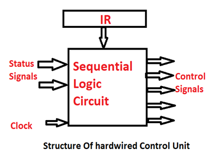
Hardwired Control Unit
Hardware control unit can be viewed as a state machine which will change from one state to another in every clock cycle depending on the content of the instruction register, external inputs and the codes used in it.The hardwired control unit is implemented as a sequential logic circuit or a finite state machine which will generate a specific sequence of the control signal to execute an instruction. The hardwired control unit uses the logic to interpret the instruction and generate control signals. While designing such type of control unit various factors are considered which are:
- Cost of designing
- Number of hardware used
- Speed of the operation (performance)
Generally, there are four techniques for designing a Hardwired control unit they are as follows:
- State table method: It is a simple method of sequential circuit design. Its attempt is to minimize the amount of hardware.
- Delay element method: It is a method which is based on the use of D flip-flop for control signal timing.
- Sequence counter method: It uses the counter for the timing purposes.
- PLA method: It uses the programmable logic array.
- It is faster than the microprogrammed control unit.
- It can be optimized to produce the fast mode of operation.
- Instruction set, the control logic is directly implemented.
- Requires change in wiring if the design has to be controlled.
- An occurrence of an error is more.
- Complex decoding and sequencing logic.
- It requires a more chip area, therefore, it is a costlier control unit.
Micro-Programmed Control Unit
In the microprogrammed control unit, microinstructions are stored in a memory called control memory. In a response to a machine instruction, a set of a microinstruction is executed by which each microinstruction will generate a set of the control signals i.e. execution of a set of microinstructions will resemble the execution of a program.A micro instruction consists of:
- One or more microinstruction to be executed
- Address of the next microinstruction to be executed
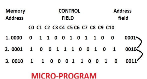
On execution of microinstructions at memory address 0000, C1, C2, C5, C7, C8 will be generated. Address of the next instruction is provided by the address field.
Functioning of micro programmed control unit:
- The control unit can generate the control signal for any instruction by sequentially reading the control word of the corresponding microprogram from the memory.
- To read the control word sequentially from the microprogram memory, a microprogram counter is needed.
- The starting address block is responsible for the loading. The starting address of the microprogram into the PC provides a new instruction which is loaded into IR.
- The PC is then automatically incremented by the clock, and it reads the successive microinstruction from the memory.
- By this, each microinstruction provides the control signal and the microprogram counters ensure that the control signal will be delivered to the various parts of the CPU in the correct sequence.
- It is both cheaper and the occurrence of an error is less.
- More flexible to accommodate with new instructions.
- Easier decoding and sequencing can be done.
- Easier to handle complex instruction sets.
- It requires a less chip area.
- This is slower than the hardwired control unit because the microinstructions are to be fetched from the control memory which is time-consuming.
Need of control unit
The control unit is very essential as a state machine circuit in which input signal is transformed into a set of output logic signals which are termed as control signals. As the control unit manages the translation of instruction and the scheduling of the microinstruction between the execution units.XO . Design counter for given sequence
CountersProblem – Design synchronous counter for sequence: 0 → 1 → 3 → 4 → 5 → 7 → 0, using T flip-flop.
Explanation – For given sequence, state transition diagram as following below:
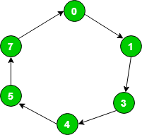
State transition table logic:
| Present State | Next State |
|---|---|
| 0 | 1 |
| 1 | 3 |
| 3 | 4 |
| 4 | 5 |
| 5 | 7 |
| 7 | 0 |
| Present State | Next State | ||||
|---|---|---|---|---|---|
| Q3 | Q2 | Q1 | Q3(t+1) | Q2(t+1) | Q1(t+1) |
| 0 | 0 | 0 | 0 | 0 | 1 |
| 0 | 0 | 1 | 0 | 1 | 1 |
| 0 | 1 | 1 | 1 | 0 | 0 |
| 1 | 0 | 0 | 1 | 0 | 1 |
| 1 | 0 | 1 | 1 | 1 | 1 |
| 1 | 1 | 1 | 0 | 0 | 0 |
| Qt | Qt+1 | T |
|---|---|---|
| 0 | 0 | 0 |
| 0 | 1 | 1 |
| 1 | 0 | 1 |
| 1 | 1 | 0 |
| Input table of Flip-Flops | |||
|---|---|---|---|
| T3 | T2 | T1 | |
| 0 | 0 | 1 | |
| 0 | 1 | 1 | |
| 1 | 1 | 0 | |
| 0 | 0 | 0 | |
| 0 | 1 | 0 | |
| 1 | 1 | 1 | |
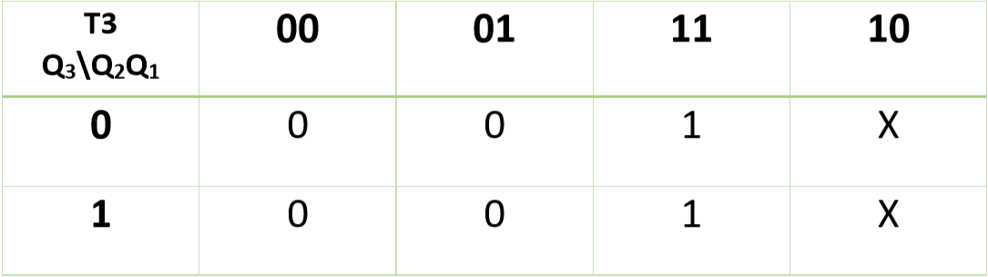
Therefore,
T3 = Q2
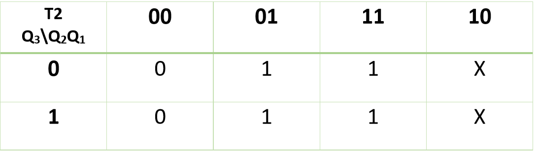
Therefore,
T2 = Q1 + Q2
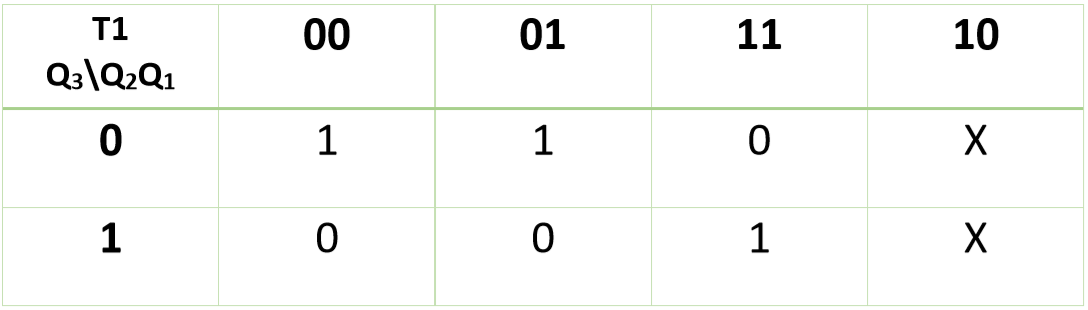
Therefore,
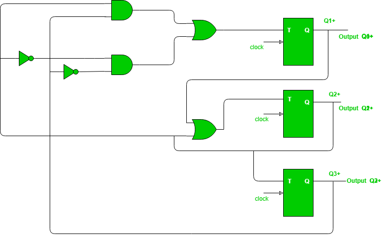
T1 = Q3’Q2’ + Q3Q2Now, you can design required circuit using expressions of K-maps:
Design of Control Unit
The Control Unit is classified into two major categories:- Hardwired Control
- Microprogrammed Control
Hardwired Control
The Hardwired Control organization involves the control logic to be implemented with gates, flip-flops, decoders, and other digital circuits.The following image shows the block diagram of a Hardwired Control organization.
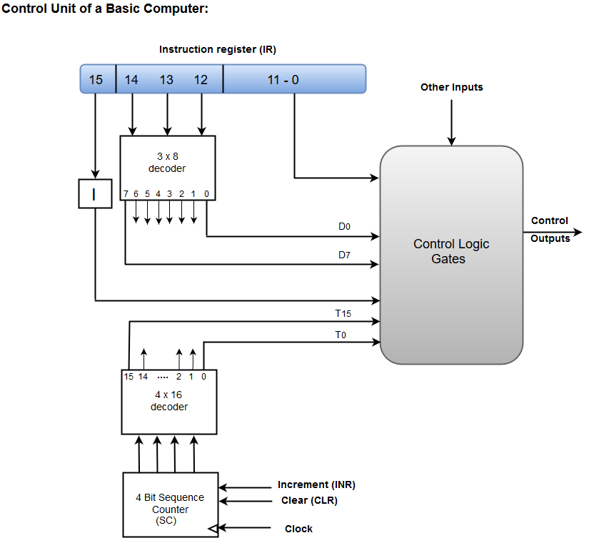
- A Hard-wired Control consists of two decoders, a sequence counter, and a number of logic gates.
- An instruction fetched from the memory unit is placed in the instruction register (IR).
- The component of an instruction register includes; I bit, the operation code, and bits 0 through 11.
- The operation code in bits 12 through 14 are coded with a 3 x 8 decoder.
- The outputs of the decoder are designated by the symbols D0 through D7.
- The operation code at bit 15 is transferred to a flip-flop designated by the symbol I.
- The operation codes from Bits 0 through 11 are applied to the control logic gates.
- The Sequence counter (SC) can count in binary from 0 through 15.
Micro-programmed Control
The Microprogrammed Control organization is implemented by using the programming approach.In Microprogrammed Control, the micro-operations are performed by executing a program consisting of micro-instructions.
The following image shows the block diagram of a Microprogrammed Control organization.
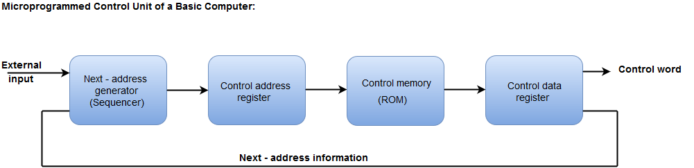
- The Control memory address register specifies the address of the micro-instruction.
- The Control memory is assumed to be a ROM, within which all control information is permanently stored.
- The control register holds the microinstruction fetched from the memory.
- The micro-instruction contains a control word that specifies one or more micro-operations for the data processor.
- While the micro-operations are being executed, the next address is computed in the next address generator circuit and then transferred into the control address register to read the next microinstruction.
- The next address generator is often referred to as a micro-program sequencer, as it determines the address sequence that is read from control memory.
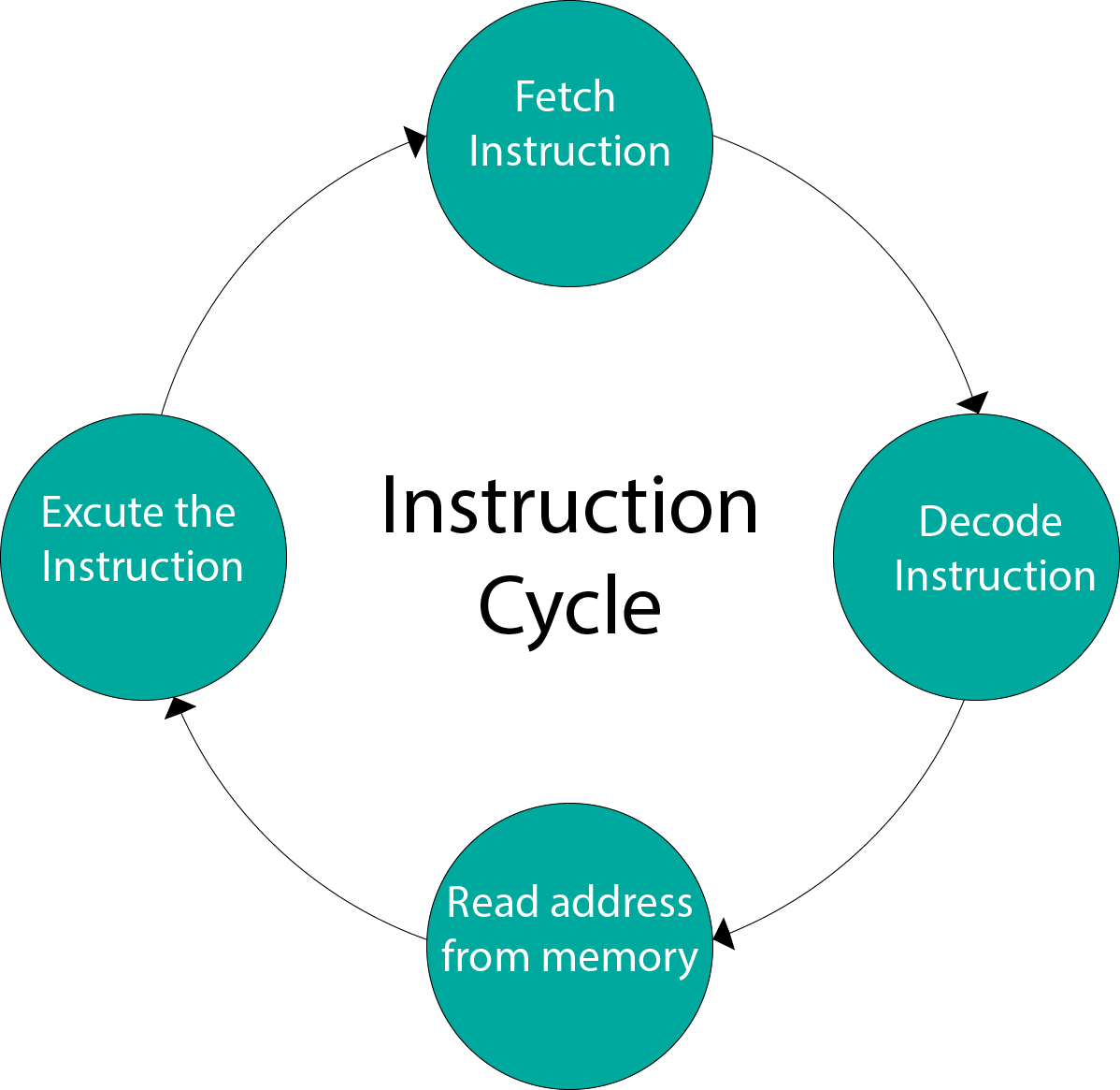
Instruction Cycle
A program residing in the memory unit of a computer consists of a sequence of instructions. These instructions are executed by the processor by going through a cycle for each instruction.In a basic computer, each instruction cycle consists of the following phases:
- Fetch instruction from memory.
- Decode the instruction.
- Read the effective address from memory.
- Execute the instruction.
Input-Output Configuration
In computer architecture, input-output devices act as an interface between the machine and the user.Instructions and data stored in the memory must come from some input device. The results are displayed to the user through some output device.
The following block diagram shows the input-output configuration for a basic computer.
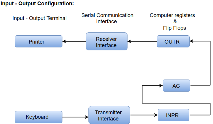
- The input-output terminals send and receive information.
- The amount of information transferred will always have eight bits of an alphanumeric code.
- The information generated through the keyboard is shifted into an input register 'INPR'.
- The information for the printer is stored in the output register 'OUTR'.
- Registers INPR and OUTR communicate with a communication interface serially and with the AC in parallel.
- The transmitter interface receives information from the keyboard and transmits it to INPR.
- The receiver interface receives information from OUTR and sends it to the printer serially.
Design of a Basic Computer
A basic computer consists of the following hardware components.- A memory unit with 4096 words of 16 bits each
- Registers: AC (Accumulator), DR (Data register), AR (Address register), IR (Instruction register), PC (Program counter), TR (Temporary register), SC (Sequence Counter), INPR (Input register), and OUTR (Output register).
- Flip-Flops: I, S, E, R, IEN, FGI and FGO
FGI and FGO are corresponding input and output flags which are considered as control flip-flops.
- Two decoders: a 3 x 8 operation decoder and 4 x 16 timing decoder
- A 16-bit common bus
- Control Logic Gates
- The Logic and Adder circuits connected to the input of AC.
Control Logic Gates
The Control Logic Gate for a basic computer is same as the one used in Hard wired Control organization.The block diagram is also similar to the Control Logic Gate used in the Hard wired Control organization.
 Inputs for the Control Logic Circuit:
- The input for the Control Logic circuit comes from the two decoders, I flip-flop and bits 0 through 11 of IR.
- The other inputs to the Control Logic are AC (bits 0 through 15), DR (bits 0 through 15), and the value of the seven flip-flops.
Outputs of the Control Logic Circuit:
- The control of the inputs of the nine registers
- The control of the read and write inputs of memory
- To set, clear, or complement the flip-flops
- S2, S1, and SO to select a register for the bus
- The control of the AC adder and logic circuit.
Digital Computers
A Digital computer can be considered as a digital system that performs various computational tasks.The first electronic digital computer was developed in the late 1940s and was used primarily for numerical computations.
By convention, the digital computers use the binary number system, which has two digits: 0 and 1. A binary digit is called a bit.
The hardware consists of all the electronic components and electromechanical devices that comprise the physical entity of the device.
The software of the computer consists of the instructions and data that the computer manipulates to perform various data-processing tasks.
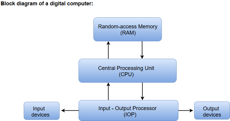
- The Central Processing Unit (CPU) contains an arithmetic and logic unit for manipulating data, a number of registers for storing data, and a control circuit for fetching and executing instructions.
- The memory unit of a digital computer contains storage for instructions and data.
- The Random Access Memory (RAM) for real-time processing of the data.
- The Input-Output devices for generating inputs from the user and displaying the final results to the user.
- The Input-Output devices connected to the computer include the keyboard, mouse, terminals, magnetic disk drives, and other communication devices.
Logic Gates
- The logic gates are the main structural part of a digital system.
- Logic Gates are a block of hardware that produces signals of binary 1 or 0 when input logic requirements are satisfied.
- Each gate has a distinct graphic symbol, and its operation can be described by means of algebraic expressions.
- The seven basic logic gates includes: AND, OR, XOR, NOT, NAND, NOR, and XNOR.
- The relationship between the input-output binary variables for each gate can be represented in tabular form by a truth table.
- Each gate has one or two binary input variables designated by A and B and one binary output variable designated by x.
AND GATE:
The AND gate is an electronic circuit which gives a high output only if all its inputs are high. The AND operation is represented by a dot (.) sign.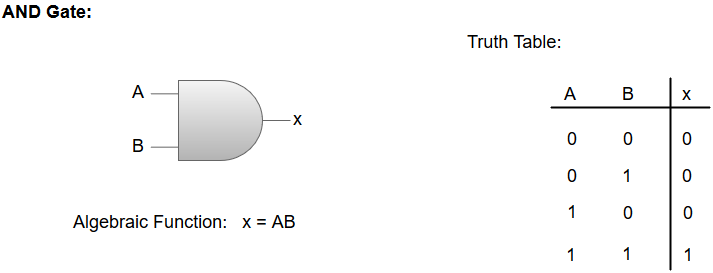
OR GATE:
The OR gate is an electronic circuit which gives a high output if one or more of its inputs are high. The operation performed by an OR gate is represented by a plus (+) sign.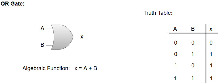
NOT GATE:
The NOT gate is an electronic circuit which produces an inverted version of the input at its output. It is also known as an Inverter.NAND GATE:
The NOT-AND (NAND) gate which is equal to an AND gate followed by a NOT gate. The NAND gate gives a high output if any of the inputs are low. The NAND gate is represented by a AND gate with a small circle on the output. The small circle represents inversion.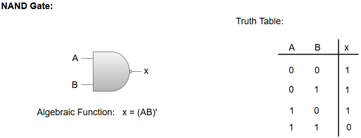
NOR GATE:
The NOT-OR (NOR) gate which is equal to an OR gate followed by a NOT gate. The NOR gate gives a low output if any of the inputs are high. The NOR gate is represented by an OR gate with a small circle on the output. The small circle represents inversion.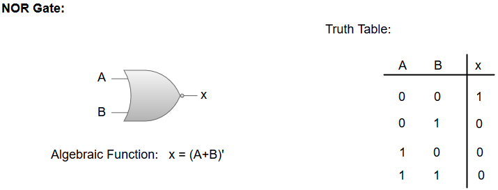
Exclusive-OR/ XOR GATE:
The 'Exclusive-OR' gate is a circuit which will give a high output if one of its inputs is high but not both of them. The XOR operation is represented by an encircled plus sign.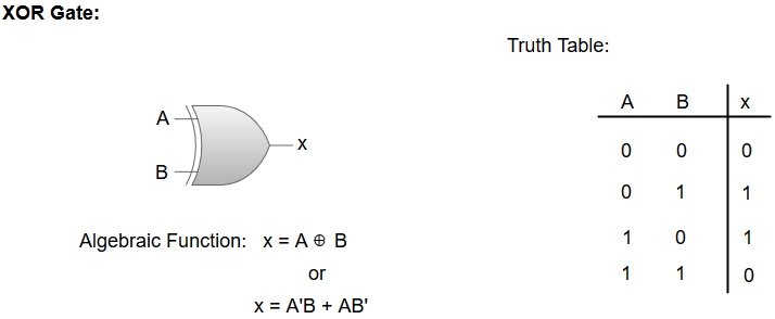
EXCLUSIVE-NOR/Equivalence GATE:
The 'Exclusive-NOR' gate is a circuit that does the inverse operation to the XOR gate. It will give a low output if one of its inputs is high but not both of them. The small circle represents inversion.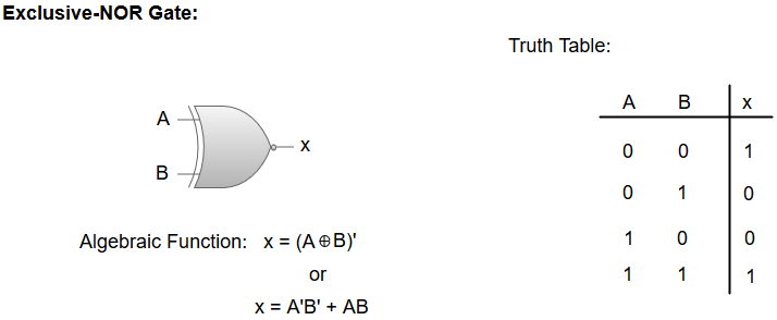
Boolean algebra can be considered as an algebra that deals with binary variables and logic operations. Boolean algebraic variables are designated by letters such as A, B, x, and y. The basic operations performed are AND, OR, and complement.
The Boolean algebraic functions are mostly expressed with binary variables, logic operation symbols, parentheses, and equal sign. For a given value of variables, the Boolean function can be either 1 or 0. For instance, consider the Boolean function:
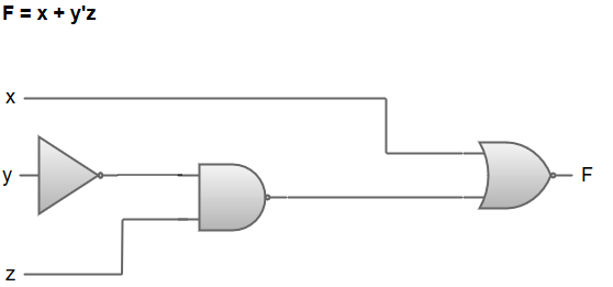
F = x + y'z
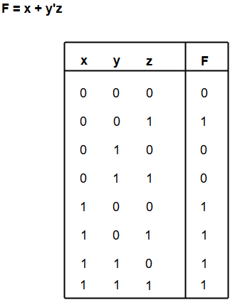
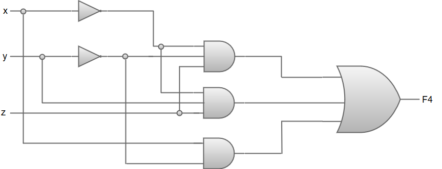
F4 = x'y'z + x'yz + xy'
Map Simplification
The Map method involves a simple, straightforward procedure for simplifying Boolean expressions.Map simplification may be regarded as a pictorial arrangement of the truth table which allows an easy interpretation for choosing the minimum number of terms needed to express the function algebraically. The map method is also known as Karnaugh map or K-map.
Each combination of the variables in a truth table is called a mid-term.
There are four min-terms in a two variable map. Therefore, the map consists of four squares, one for each min-term. The 0's and 1's marked for each row, and each column designates the values of variable x and y, respectively.
Two-variable map:
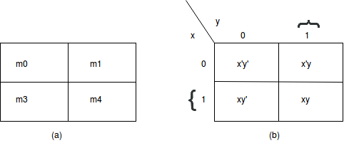 Representation of functions in the two-variable map:
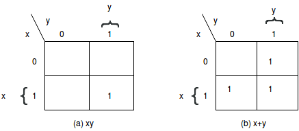
Three variable map
There are eight min-terms in a three-variable map. Therefore, the map consists of eight squares.Three variable map:
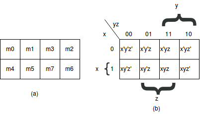
- The map was drawn in part (b) in the above image is marked with numbers in each row and each column to show the relationship between the squares and the three variables.
- Any two adjacent squares in the map differ by only one variable, which is primed in one square and unprimed in the other. For example, m5 and m7 lie in the two adjacent squares. Variable y is primed in m5 and unprimed in m7, whereas the other two variables are the same in both the squares.
- From the postulates of Boolean algebra, it follows that the sum of
two min-terms in adjacent squares can be simplified to a single AND term
consisting of only two literals. For example, consider the sum of two
adjacent squares say m5 and m7:
m5+m7 = xy'z+xyz= xz(y'+y)= xz.
Examples of Boolean algebra simplifications using the map method
1. F(x,y,z) = Σ (2,3,4,5)First, 1 is marked in each min-term that represents the function. Hence, 010, 011, 100, 101 are marked with 1's.
Subsequently, we have to find possible adjacent squares. These are indicated in the map by two rectangles, each enclosing two 1's.
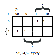 The upper right rectangle represents the area enclosed by x'y.
The lower left rectangle represents the product term xy'.
The sum of these two terms gives the simplified expression:
F= x'y+ xy'
Algebraically verification:
m0+m2 = x'y'z'+ x'yz'= x'z'(y'+y) = x'z'
m4+m6 = xy'z' + xyz'= xz' + (y'+y) = xz'
2. F(x,y,z) = Σ(3,4,6,7)
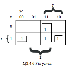 As you can see, there are four squares marked with 1's, one for each min-term of the function.
The other two adjacent squares are combined in the third column to give a two-literal term yz.
The remaining two squares with 1's are shown in the above diagram with their values enclosed in half rectangles. When these two half rectangles are combined, it yields two literal term xz'.
The simplified function becomes F= yz+xz'.
Combinational Circuits
A combinational circuit comprises of logic gates whose outputs at any time are determined directly from the present combination of inputs without any regard to previous inputs.A combinational circuit performs a specific information-processing operation fully specified logically by a set of Boolean functions.
The basic components of a combinational circuit are: input variables, logic gates, and output variables.
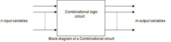 The 'n' input variables come from an external source whereas the 'm'
output variables go to an external destination. In many applications,
the source or destination are storage registers.
The 'n' input variables come from an external source whereas the 'm'
output variables go to an external destination. In many applications,
the source or destination are storage registers.Design procedure of a Combinational Circuit
The design procedure of a combinational circuit involves the following steps:- The problem is stated.
- The total number of available input variables and required output variables is determined.
- The input and output variables are allocated with letter symbols.
- The exact truth table that defines the required relationships between inputs and outputs is derived.
- The simplified Boolean function is obtained from each output.
- The logic diagram is drawn.
S-R Flip-flop/Basic Flip-Flop
Flip flops are an application of logic gates. A flip-flop circuit can remain in a binary state indefinitely (as long as power is delivered to the circuit) until directed by an input signal to switch states.S-R flip-flop stands for SET-RESET flip-flops.
The SET-RESET flip-flop consists of two NOR gates and also two NAND gates.
These flip-flops are also called S-R Latch.
The design of these flip flops also includes two inputs, called the SET [S] and RESET [R]. There are also two outputs, Q and Q'.
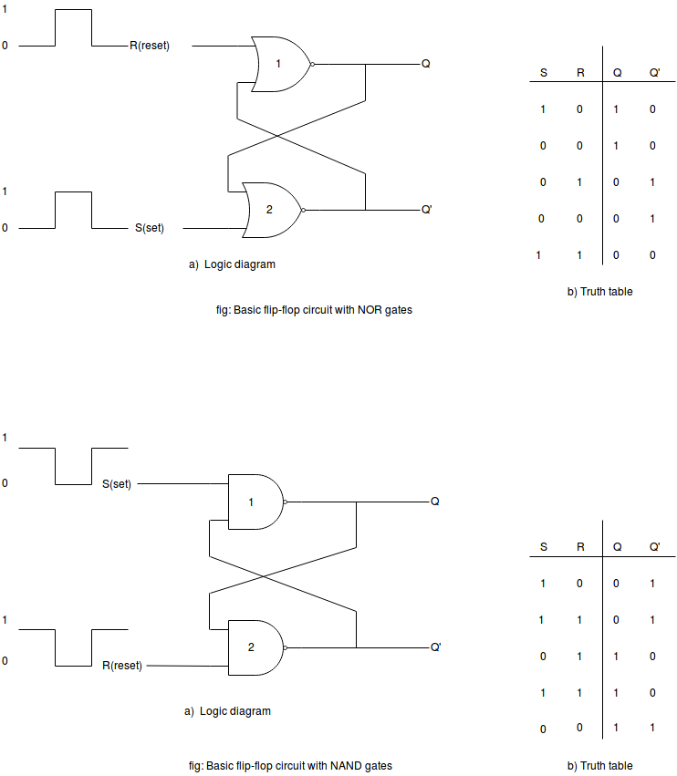
Clocked S-R Flip-Flop
The operation of a basic flip-flop can be modified by providing an additional control input that determines when the state of the circuit is to be changed.The limitation with a S-R flip-flop using NOR and NAND gate is the invalid state. This problem can be overcome by using a stable SR flip-flop that can change outputs when certain invalid states are met, regardless of the condition of either the Set or the Reset inputs.
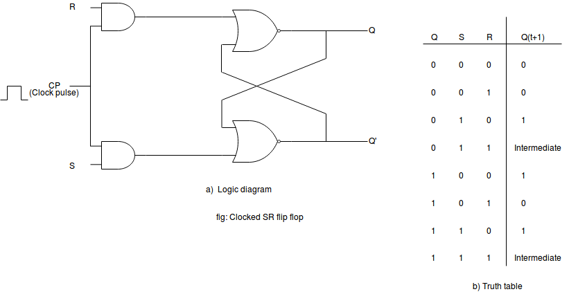 A clock pulse is given to the inputs of the AND Gate. If the value of
the clock pulse is '0', the outputs of both the AND Gates remain '0'.
A clock pulse is given to the inputs of the AND Gate. If the value of
the clock pulse is '0', the outputs of both the AND Gates remain '0'.D Flip-Flop
D flip-flop is a slight modification of clocked SR flip-flop.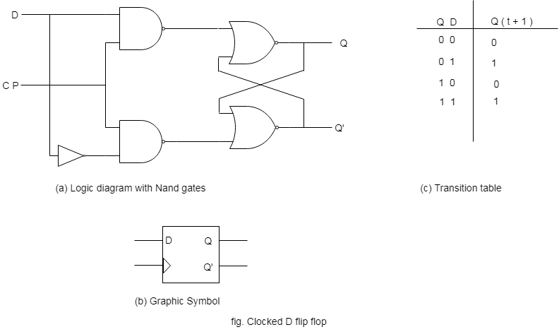 From the above figure, you can see that the D input is connected to
the S input and the complement of the D input is connected to the R
input.
From the above figure, you can see that the D input is connected to
the S input and the complement of the D input is connected to the R
input.When the value of CP is '1' (HIGH), the flip-flop moves to the SET state if it is '0' (LOW), the flip-flop switches to the CLEAR state.
J-K Flip-Flop
J-K flip-flop can be considered as a modification of the S-R flip-flop.The main difference is that the intermediate state is more refined and precise than that of an S-R flip-flop.
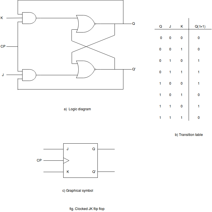 The characteristics of inputs 'J' and 'K' is same as the 'S' and 'R' inputs of the S-R flip-flop.
J stands for SET, and 'K' stands for CLEAR.
When both the inputs J and K have a HIGH state, the flip-flop switches to the complement state, so, for a value of Q = 1, it switches to Q=0, and for a value of Q = 0, it switches to Q=1.
T Flip-Flop
T flip-flop is a much simpler version of the J-K flip-flop.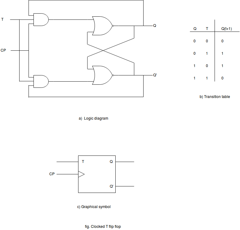 Both the J and K inputs are connected and are also called as a single input J-K Flip-flop.
Triggering of Flip-Flops
The state of the flip-flop is changed by a momentary change in the input signal. This momentary change is known as Trigger, and the transition it causes is said to triggering the flip-flop.Pulses trigger clocked flip-flops.
A pulse start from the initial value of '0', goes momentarily to '1', and after a short while, returns to its initial '0' value.
A clock pulse is either positive or negative.
A positive clock source remains at '0' during the interval between pulses and goes to 1 during the occurrence of a pulse.
The pulse goes through two signal transition: from '0' to '1' and return from '1' to '0'.
Definition of clock pulse transition:
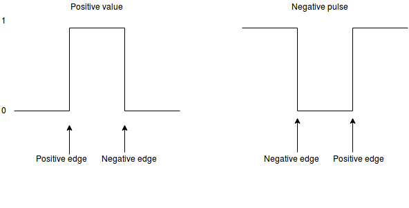 The positive transition is defined as a positive edge and the negative transition as a negative edge.
Ripple Counter
A ripple counter is an asynchronous counter where only the first flip-flop is clocked by an external clock. All subsequent flip-flops are clocked by the output of the preceding flip-flop. Asynchronous counters are also called ripple-counters because of the way the clock pulse ripples it way through the flip-flops.The MOD of the ripple counter or asynchronous counter is 2n if n flip-flops are used. For a 4-bit counter, the range of the count is 0000 to 1111 (24-1). A counter may count up or count down or count up and down depending on the input control. The count sequence usually repeats itself. When counting up, the count sequence goes from 0000, 0001, 0010, ... 1110 , 1111 , 0000, 0001, ... etc. When counting down the count sequence goes in the opposite manner: 1111, 1110, ... 0010, 0001, 0000, 1111, 1110, ... etc.
The complement of the count sequence counts in reverse direction. If the uncomplemented output counts up, the complemented output counts down. If the uncomplemented output counts down, the complemented output counts up.
There are many ways to implement the ripple counter depending on the characteristics of the flip flops used and the requirements of the count sequence.
- Clock Trigger: Positive edged or Negative edged
- JK or D flip-flops
- Count Direction: Up, Down, or Up/Down
It can be implemented using D-type flip-flops or JK-type flip-flops.
The circuit below uses 2 D flip-flops to implement a divide-by-4 ripple counter (2n = 22 = 4). It counts down.
-
Notes:
- Click on CLK (Red) switch and observe the changes in the outputs of the flip flops. The CLK switch is a momentary switch (similar to a door bell switch - normally off).
- PR and CLR are both connected to VCC (set to 1)
- The D flip flop clock has a rising edge CLK input. For example Q0 behaves as follows:
- The D input value just before the CLK rising edge is noted (Q00).
- When CLK rising edge occurs, Q0 is assigned the previously noted D value (Q00).
- Thus, whenever a rising edge appears at the CLK of the D flip flop, the output Q changes state (or toggles).
- The MOD or number of unique states of this 2 flip flop ripple counter is 4 (22).
- Simulate and Breadboard the Ripple Counter circuit.
- A Truncated Ripple Counter is used if a MOD of less than 2n is required. For example, if you want to change the sequence from 3,2,1,0,3,2,1,0 ... to 3,2,0,3,2,0 ...
Timing and Control
All sequential circuits in the Basic Computer CPU are driven by a master clock, with the exception of the INPR register.At each clock pulse, the control unit sends control signals to control inputs of the bus, the registers, and the ALU.
Control unit design and implementation can be done by two general methods:
-
A hardwired control unit is designed
from scratch
using traditional digital logic design techniques to produce
a minimal, optimized circuit. In other words, the control unit
is like an ASIC (application-specific integrated circuit).
-
A microprogrammed control unit is built from
some sort of ROM. The desired control signals are simply stored
in the ROM, and retrieved in sequence to drive the microoperations
needed by a particular instruction.
we use primarily the timing signals and bits from the instruction register to construct control functions. These are the independent variables in the CPU. Control inputs on CPU components, such as ACload, S0, etc. are dependent variables, i.e. functions of the timing signals and IR bits.
The following components provide most of the independent variables for the Boolean functions driving control inputs such as ACLD, PCINR, etc.
- I flip-flop
- Opcode field from the instruction code
- Address bits from the instruction code
- 4-bit counter with INR, CLR (CLR=1 at power-on)
indicates the following control function and microoperation:
D3T4: SCCLR
Xie . How to Increment a Counter in Word
Microsoft Word includes fields that enable customized data insertion, including Word Count, Page Count and Sequence, which is used to create incremental counters. You can create a business plan using numbered content such as headings or paragraphs, or a simple table with numbered row blocks using the “SEQ” field name.
2.Click the “Insert” tab at the top of the application. Click “Quick Parts” in the Text group and choose “Field.”
3.Scroll
through the “Field Names” section and choose “Seq.” In the “Field
Codes” field, next to the “SEQ” text, type an identifier such as “mynum”
or “seqnum” to create the first number.
4. Add
numbers by inserting the same identifier at another location.
Alternatively, copy the first one, select it and press “F9” to update
the display. As a third option, you can use the keyboard shortcut
“Ctrl-F9” and type “SEQ” and your identifier between the braces that
appear. For instance, insert “{SEQ mynum}.” Press “F9” to update the
field and enable the number to display.
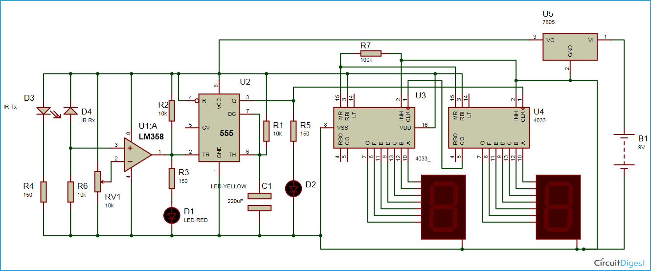
2 digit object counter circuit diagram using ic 555 & lm358 automatic object counter circuit diagram .
whereas if in a computer monitor seven segments can be measured in the number of pixels, so the more pixels, the more object words and electronic sequences above we develop into more seven segments, the electronic circuit above is only for 2 words or 2 bytes or 2 characters .
whereas if in a computer monitor seven segments can be measured in the number of pixels, so the more pixels, the more object words and electronic sequences above we develop into more seven segments, the electronic circuit above is only for 2 words or 2 bytes or 2 characters . in computer electronics there are 240 bytes and 240 characters + Numeric Lock. All of them are coded in ASCII (American Standard) counter code characters .
the example Alarm / Bel with Counter in electronic circuit


Position Counter Electronic

DATA MATRIX
An example of a Data Matrix code, encoding the text .
_________________________________________________________________________________

Gen. Mac Tech Zone e- Count Rolling for Tour Back to basic Reroute