MARIA PREFER to obtain partial temporary power input via a voltage doubler as the connecting power of active blocks from one electronic circuit to another electronic circuit stage (input - block 1 - block 2 - output - block setting / control loop electronics block ) AMNIMARJESLOW GOVERNMENT 9132047010017 Tsu no denshi kairo kara betsu no denshi kairo sutēji e no Akutibu burokku no setsuzoku denryoku to shite no den'atsu daburā (nyūryoku - burokku 1 - burokku 2 - shutsuryoku - burokku settei) rūpuburokku seigyo 02096010014 LJBUS TRACK __X Thankyume on Lord Jesus About : O Lord, Your love reaches the heavens, Your faithfulness reaches the clouds, You uphold the earth, so that it will remain there. "" The endless love of the LORD, His endless blessings and love, always new every morning; great is your faithfulness! "Your love and your truth remain firm from the side of life before - now and for the future and for the foreseeable future __ Gen. Mac Tech Zone MARIA PREFER in reducing the decrease in power from the electronic block in Maria's system so that the power strength remains stable even strengthened. )
Current doubler and Voltage Multipliers (Doublers, Triplers, Quadruplers, and More)
In a low-voltage high-current SMPS, the secondary voltage is often rectified with the help of centre-tapped configuration.
The main advantage is that at any instant of time just one diode is
rectifying (as compared to the full-wave bridge rectifier). This
improves energy efficiency, because the forward voltage drop on the
diode (e.g. 0.7 V) can be a significant proportion of the output voltage
(e.g. 3 V). The main disadvantage of such approach is that the transformer is oversized, because only half of the secondary winding conducts at any time. For low voltage applications the secondary winding might have very few
turns (usually just one or two), which complicates selection of an
appropriate turn ratio of the transformer.
Current doubler alleviates such problems. Finer control over turns ratio
is possible, because the secondary voltage of the transformer is higher
and the current is doubled outside of the transformer. Some manufacturers supply magnetic components or accessories for making dedicated current doublers.
A transformer Tx is driven in a bipolar way (push-pull, half-bridge or full-bridge). Two identical inductorsL1 and L2 are connected across the secondary winding of Tx. These inductors are not magnetically coupled to each other or to the main transformer.
Because of bipolarity, an alternating voltage is driven across the two inductors connected in series. The load R
is connected between the central point of the inductors (similar to a
regular centre-tap configuration) and the shorted output of the two
diodes D1 and D2. The low-pass filter can be implemented as the capacitor C, or as an additional output inductor (not shown).
Operation
The name “current doubler” comes from the fact that the average output
current of the whole device is twice the average currents in each of the
output inductors.
Current and voltage waveforms - the output current is a sum of the two inductor currents
However, the RMS value which are responsible for temperature increase of the windings depend on the DC offset in each current. If the current ripple
is very high, then the RMS values increase accordingly and become
comparable with the RMS value of the total output current. Under such
conditions the “doubling” property of the topology is not utilised
properly.
For this reason, the current doubler is usually operated in continuous conduction mode,
so that the currents in the two output inductors keep flowing at all
times, with large DC offsets and relatively small ripple, which reduces
the RMS values. This is achieved by using proportionally larger inductance
of the output inductors. Under such conditions the average value of the
output current remains the same, but its RMS is twice the inductor
currents. Additionally, the ripple in the output current is also reduced
by half. This occurs because most of the time one current increases and
the other decreases, so the ripple in their sum appears accordingly
reduced, as shown in the waveforms.
Typical current waveforms with low DC offset (inductance too low)
The
voltage multiplier is an electronic circuit that delivers
the output voltage
whose amplitude (peak value) is two, three, or more
times greater than the amplitude (peak value) of the input
voltage.
or
The
voltage multiplier is an electronic circuit that converts
the low AC voltage into high DC voltage.
or
The
voltage multiplier is an AC-to-DC converter, made up of diodes
and capacitors
that produce a high voltage DC output from a low
voltage AC input.
What is
voltage multiplier?
Voltage
multiplier
power supplies have been used for many years. Walton and
Cockroft built an 800 kV supply for an ion accelerator in
1932. Since that time the voltage multiplier has been used
primarily when high voltages and low currents are required.
The use of voltage multiplier circuits reduces the size of
the high voltage transformer and, in some cases, makes it
possible to eliminate the transformer.
The
recent technological developments have made it possible to
design a voltage multiplier that efficiently converts the
low AC voltage into high DC voltage comparable to that of
the more conventional transformer-rectifier-filter-circuit.
The
voltage multiplier is made up of capacitors and diodes that
are connected in different configurations. Voltage
multiplier has different stages. Each stage is made up of
one diode and one capacitor. These arrangements of diodes
and capacitors make it possible to produce rectified and filtered
output voltage whose amplitude (peak value) is
larger than the input AC voltage.
Types of
voltage multipliers
Voltage
multipliers
are classified into four types:
Half-wave
voltage doubler
Full-wave
voltage doubler
Voltage
tripler
Voltage
quadrupler
Half-wave
voltage doubler
As
its name suggests, a half-wave voltage doubler is a voltage
multiplier circuit whose output voltage amplitude is twice
that of the input voltage amplitude. A half-wave voltage
doubler drives the voltage to the output during either
positive or negative half cycle. The half-wave voltage
doubler circuit consists of two diodes, two capacitors, and
AC input voltage source.
During positive
half cycle:
The
circuit diagram of the half-wave voltage doubler is shown in
the below figure. During the positive half cycle, diode D1
is forward
biased. So it allows electric
current through it. This current will flows to the
capacitor C1 and
charges it to the peak value of input voltage I.e. Vm.
However,
current does not flow to the capacitor C2 because
the diode D2 is reverse
biased. So the diode D2 blocks the electric
current flowing towards the capacitor C2.
Therefore, during the positive half cycle, capacitor C1
is charged whereas capacitor C2 is uncharged.
During negative
half cycle:
During
the negative half cycle, diode D1 is reverse
biased. So the diode D1 will not allow electric
current through it. Therefore, during the negative half
cycle, the capacitor C1 will not be charged.
However, the charge
(Vm) stored in the capacitor C1
is discharged (released).
On
the other hand, the diode D2 is forward biased
during the negative half cycle. So the diode D2
allows electric current through it. This current will flows
to the capacitor C2 and charges it. The capacitor
C2 charges to a value 2Vm because the
input voltage Vm and
capacitor C1 voltage Vm is added to
the capacitor C2. Hence, during the negative half
cycle, the capacitor C2 is charged by both input
supply voltage Vm and capacitor C1
voltage Vm. Therefore, the capacitor C2
is charged to 2Vm.
If
a load is connected to the circuit at the output side, the
charge (2Vm) stored in the capacitor C2
is discharged and flows to the output.
During
the next positive half cycle, diode D1 is forward
biased and diode D2 is reverse biased. So the
capacitor C1 charges to Vm whereas
capacitor C2 will not be charged. However, the
charge (2Vm) stored in the capacitor C2
will be discharged and flows to the output load. Thus, the
half-wave voltage doubler drives a voltage of 2Vm to
the output load.
The
capacitor
C2 gets charged again in the next half cycle.
The
voltage (2Vm) obtained at the output side is
twice that of the input voltage (Vm).
The
capacitors
C1 and C2 in half wave-voltage doubler
charges in alternate half cycles.
The
output waveform of the half-wave voltage doubler is almost
similar to the half
wave rectifier with filter. The only difference is the
output voltage amplitude of the half-wave voltage doubler is
twice that of the input voltage amplitude but in half wave
rectifier with filter, the output voltage amplitude is same
as the input voltage amplitude.
The
half-wave
voltage doubler supplies the voltage to the output load in
one cycle (either positive or negative half cycle). In our
case, the half-wave voltage doubler supplies the voltage to
the output load during positive half cycles. Therefore,
the output signal regulation of the half-wave voltage
doubler is poor.
Advantages of
half-wave voltage doubler
High
voltages
are produced from the low input voltage source without using
the expensive high voltage transformers.
Disadvantages of
half-wave voltage doubler
Large
ripples (unwanted fluctuations) are present in the output
signal.
Full-wave
voltage doubler
The
full-wave
voltage doubler consists of two diodes, two capacitors, and
input AC voltage source.
During positive
half cycle:
During
the positive half cycle of the input AC signal, diode D1
is forward biased. So the diode D1 allows
electric current through it. This current will flows to the
capacitor C1 and charges it to the peak value of
input voltage I.e Vm.
On
the other hand, diode D2 is reverse biased during
the positive half cycle. So the diode D2 does not
allow electric current through it. Therefore, the capacitor
C2 is uncharged.
During negative
half cycle:
During
the negative half cycle of the input AC signal, the diode D2
is forward biased. So the diode D2 allows
electric current through it. This current will flows to the
capacitor C2 and charges it to the peak value of
the input voltage I.e. Vm.
On
the other hand, diode D1 is reverse biased during
the negative half cycle. So the diode D1 does not
allow electric current through it.
Thus, the capacitor C1
and capacitor C2 are charged during alternate
half cycles.
The
output voltage is taken across the two series connected
capacitors C1 and C2.
If
no load is connected, the output voltage is equal to the sum
of capacitor C1 voltage and capacitor C2
voltage I.e. C1 + C2 = Vm +
Vm = 2Vm. When a load is connected to
the output terminals, the output voltage Vo will
be somewhat less than 2Vm.
The
circuit is called full-wave voltage doubler because one of
the output capacitors is being charged during each half
cycle of the input voltage.
Voltage
tripler
The
voltage tripler can be obtained by adding one more
diode-capacitor stage to the half-wave voltage doubler
circuit.
During first
positive half cycle:
During
the first positive half cycle of the input AC signal, the
diode D1 is forward biased whereas diodes D2
and D3 are reverse biased. Hence, the diode D1
allows electric current through it. This current will flows
to the capacitor C1 and charges it to the peak
value of the input voltage I.e. Vm.
During negative
half cycle:
During
the negative half cycle, diode D2 is forward
biased whereas diodes D1 and D3 are
reverse biased. Hence, the diode D2 allows
electric current through it. This current will flows to the
capacitor C2 and charges it. The capacitor C2
is charged to twice the peak voltage of the input
signal (2Vm). This is because the charge (Vm)
stored in the capacitor C1 is discharged during
the negative half cycle.
Therefore,
the
capacitor C1 voltage (Vm) and the
input voltage (Vm) is added to the capacitor C2
I.e Capacitor voltage + input voltage = Vm + Vm
= 2Vm. As a result, the capacitor C2
charges to 2Vm.
During second
positive half cycle:
During
the second positive half cycle, the diode D3 is
forward biased whereas diodes D1 and D2
are reverse biased. Diode D1 is reverse biased
because the voltage at X is negative due to charged voltage
Vm, across C1 and
diode D2 is reverse biased because of its
orientation. As a result, the voltage (2Vm)
across capacitor C2 is discharged. This charge
will flow to the capacitor C3 and charges it to
the same voltage 2Vm.
The
capacitors
C1 and C3 are in series and the output
voltage is taken across the two series connected capacitors
C1 and C3. The voltage across
capacitor C1 is Vm and capacitor C3
is 2Vm. So the total output voltage is equal to
the sum of capacitor C1 voltage and capacitor C3
voltage I.e. C1 + C3 = Vm +
2Vm = 3Vm.
Therefore,
the
total output voltage obtained in voltage tripler is 3Vm
which is three times more than the applied input voltage.
Voltage
quadrupler
The
voltage quadrupler can be obtained by adding one more
diode-capacitor stage to the voltage tripler circuit.
During first
positive half cycle:
During
the first positive half cycle of the input AC signal, the
diode D1 is forward biased whereas diodes D2,
D3
and D4 are reverse biased. Hence, the diode D1
allows electric current through it. This current will flows
to the capacitor C1 and charges it to the peak
value of the input voltage I.e. Vm.
During first
negative half cycle:
During
the first negative half cycle, diode D2 is
forward biased and diodes D1, D3
and D4 are reverse biased. Hence, the diode D2
allows electric current through it. This current will flows
to the capacitor C2 and charges it. The capacitor
C2 is charged to twice the peak voltage of the
input signal (2Vm). This is because the charge (Vm)
stored in the capacitor C1 is discharged during
the negative half cycle.
Therefore,
the
capacitor C1 voltage (Vm) and the
input voltage (Vm) is added to the capacitor C2
I.e Capacitor voltage + input voltage = Vm + Vm
= 2Vm. As a result, the capacitor C2
charges to 2Vm.
During second
positive half cycle:
During
the second positive half cycle, the diode D3 is
forward biased and diodes D1, D2
and D4 are reverse biased. Diode D1 is
reverse biased because the voltage at X is negative due to
charged voltage Vm, across C1
and, diode D2 and D4 are
reverse biased because of their orientation. As a result,
the voltage (2Vm) across capacitor C2
is discharged. This charge will flow to the capacitor C3
and charges it to the same voltage 2Vm.
During second
negative half cycle:
During
the second negative half cycle, diodes D2 and D4
are forward biased whereas diodes D1 and D3
are reverse biased. As a result, the charge (2Vm)
stored in the capacitor C3 is discharged. This
charge will flow to the capacitor C4 and charges
it to the same voltage (2Vm).
The
capacitors
C2 and C4 are in series and the output
voltage is taken across the two series connected capacitors
C2 and C4. The voltage across
capacitor C2 is 2Vm and capacitor C4
is 2Vm. So the total output voltage is equal to
the sum of capacitor C2 voltage and capacitor C4
voltage I.e. C2 + C4 = 2Vm
+ 2Vm = 4Vm.
Therefore,
the
total output voltage obtained in voltage quadrupler is 4Vm
which is four times more than the applied input voltage.
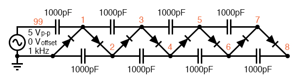
Cockcroft-Walton x8 voltage multiplier; output at v(8).
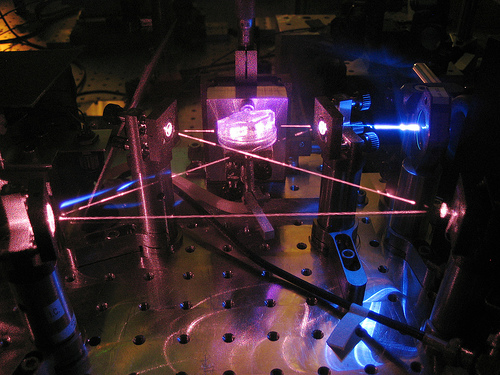
LASER TECHNOLOGY
TECHNOLOGY LASER ON PCB LAYER
If you need a high voltage, a voltage multiplier is one of
the easiest ways to obtain it. A voltage multiplier is a specialized
type of rectifier circuit that converts an AC voltage to a higher DC
voltage. Invented by Heinrich Greinacher in 1919, they were used in the design of a particle accelerator that performed the first artificial nuclear disintegration, so you know they mean business.
Theoretically the output of the multiplier is an integer times the AC
peak input voltage, and while they can work with any input voltage, the
principal use for voltage multipliers is when very high voltages, in
the order of tens of thousands or even millions of volts, are needed.
They have the advantage of being relatively easy to build, and are
cheaper than an equivalent high voltage transformer of the same output
rating. If you need sparks for your mad science, perhaps a voltage
multiplier can provide them for you.
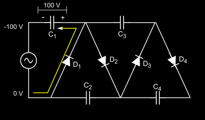
How Does It Work?
The multiplier circuit needs an AC power supply in order to work. For the sake of simplicity let´s assume that one
side of the power supply is grounded and remains at zero potential, and
the other varies between plus and minus U (100 V in the example).
Here’s what happens:
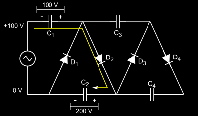
Capacitor C1 charges through diode D1 at the
voltage U (100 V) of the power supply, which is at its negative peak.
Note that this leads the capacitor to be positive at its right side and
negative at its left. The yellow line indicates the direction of
current flow
We now have +100 V at the upper side of the power supply, and this voltage adds to that of C1 that was charged in the previous step. Therefore capacitor C2 charges through D2 to 200 V, or 2U (100 V from the power supply plus 100 V from C2).
The charge stored in C1 was used in the previous cycle to charge C2, so C1 is now charging through D1 as in step 1. Also, capacitor C3 is charged through D3 to 2U. Why 2U? Because since C1 is discharged, point “a” in the schematic is at zero potential and C3 sees the 200 V of C2.
The power supply is again at its positive peak, and C2 is now being recharged as in step 2. At the same time, capacitor C4 charges
to 200 V, because it is the potential difference that it sees: 400 V at
its positive side (100 V of the supply plus 100 V of C1 plus 200 V of C3), and 200 V at its negative side, which is the potential of C2.
As we can see, we will end with 400 V between ground and the output
(points a and b in the last figure), effectively quadrupling the supply
voltage.
This is an idealized explanation, and as you may guess reality is
always more complicated. For instance, capacitors do not charge
instantly, therefore they do not reach the full voltage until several
cycles have passed, depending on the charging current that the power
supply can deliver.
The multiplier that we just discussed has two stages. Each stage is
formed by two capacitors and two diodes and each one adds two times the
voltage of the power supply, so for example a five-stage multiplier will
have an output of ten times the input voltage. Note that each component
in the circuit only sees at most twice the peak input voltage provided
by the source, therefore you can use low voltage components and many
stages to obtain a very high output voltage. However,
the output voltage will drop as soon as you connect a load to the
circuit, according to this formula. Here we can see that we need high
frequency and high capacitance in order to minimize voltage drop, and
that this drop increases with current, and also very rapidly with the
number of stages. In fact, since it depends on the cube of the number of
stages, a multiplier with ten stages has 1000 times more voltage drop
than one with a single stage.
Another situation that arises when very high voltages are present is corona
discharge, which is an electrical discharge that arises when the
strength of the electric field around a conductor is high enough. Corona
acts as an unwanted load on the multiplier, reducing the output power.
One way to minimize corona is to reduce the curvature in conductors,
avoiding sharp corners, projecting points and small diameter wires. For
this reason large diameter end points and conductors are used. This of
course complicates the design of very high voltage multipliers but at
the same time accounts for their impressive look, as in the feature
image.
Homemade voltage multiplier, by [rmcybernetics]Making a voltage multiplier to obtain high voltage is a popular project
and is pretty easy as long as the voltage is not too high for corona to
start creating problems. All you need besides an AC power supply such
as a neon transformer
are some high voltage diodes and capacitors. Practical uses include
X-ray machines, photocopiers, air ionizers and microwave ovens, among
others. At the high end of the spectrum are the multipliers used for
research in particle accelerators, several meters in height, that can
reach millions of volts.


/cdn.vox-cdn.com/uploads/chorus_asset/file/11445439/production_2.jpg)
 one
side of the power supply is grounded and remains at zero potential, and
the other varies between plus and minus U (100 V in the example).
Here’s what happens:
one
side of the power supply is grounded and remains at zero potential, and
the other varies between plus and minus U (100 V in the example).
Here’s what happens: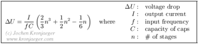 However,
the output voltage will drop as soon as you connect a load to the
circuit, according to this formula. Here we can see that we need high
frequency and high capacitance in order to minimize voltage drop, and
that this drop increases with current, and also very rapidly with the
number of stages. In fact, since it depends on the cube of the number of
stages, a multiplier with ten stages has 1000 times more voltage drop
than one with a single stage.
However,
the output voltage will drop as soon as you connect a load to the
circuit, according to this formula. Here we can see that we need high
frequency and high capacitance in order to minimize voltage drop, and
that this drop increases with current, and also very rapidly with the
number of stages. In fact, since it depends on the cube of the number of
stages, a multiplier with ten stages has 1000 times more voltage drop
than one with a single stage.
 power supply, and this voltage adds to that of C1 that was charged in the previous step. Therefore capacitor C2 charges through D2 to 200 V, or 2U (100 V from the power supply plus 100 V from C2).
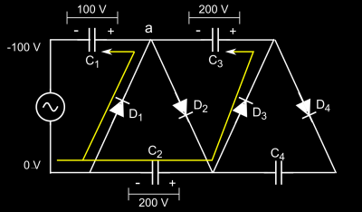 Why 2U? Because since C1 is discharged, point “a” in the schematic is at zero potential and C3 sees the 200 V of C2.
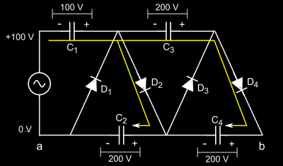 potential of C2.
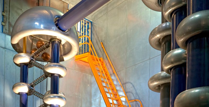
Tidak ada komentar:
Posting Komentar