POWER ELECTRONICS


Power Electronics (Power Electronics) is defined as an electronic application that focuses on setting up large power electrical equipment by way of conversion of electrical parameters (current, voltage, power). Here is intended circuit electronics applications that use electronic equipment, especially semiconductors that functioned as a switch (switching) to make arrangements by way of conversion of source type AC - AC, AC - DC, DC - DC and DC - AC. Semiconductor devices used are solid-state electronics to make arrangements more efficient the system that has the power and energy were great. Power electronics application has the following characteristics:
1. Application control techniques to get
2. Electronic power is a combination of various disciplines namely Power Engineering, Electronics and control systems technology.
3. Electronic power using power electronics components (solid-state) to control and convert electric power
4. The power electronics circuit consists of input and load (load).
5. The power electronics circuit may consist of one or more converter to change parameters of electricity.
thyristor
The thyristor is one power semiconductor devais most important and has been used extensively in power electronics circuits. The thyristor is usually used as a switch / bistable, operating between non-conduction state to the conduction. In many applications, the thyristor can be assumed as an ideal switch but in practice thyristor has a limited and specific characteristics.
Various Thyristor
Consists of several kinds of them:
SCR (Silicon Controlled Rectifier)
DIAC
TRIAC (triode AC switch)
PUT (Programmable Uni-junction transistors)
UJT (Uni-Junction Transistor)
GTO (Gate Turn Off Thyristor)
DB-GTO (Distributed Buffer - Ggate Turn-off Thyristor)
LASCR (Light Activated Silicon Controlled Rectifier)
RCT (Reverse Conduction Thyristor)
SITH (Static Induction Thyristor)
MOS-Controlled Thyristor (MCT)
IGCT (Integrated Gate commutated thyristor)
Composite MOS Static Induction Thyristor / CSMT
MCT (MOS Controlled Thyristor)
X . I Understanding the power electronics
Understanding the power electronics is one branch of electronics that has nothing to do with how to process and regulate electrical power electronically. The linkage of power electronics on how to cultivate and process the electrical energy, namely the use of electronic devices for converting an electric power to the control and modification of the form of voltage or current so that there forms a transformation other forms. When viewed from the scope of the power electronics include: Computer Components and Semiconductors; Electronics; Electricity System; Electrical circuit theory; Electrical Machinery; Control System; and electro magnetics.
Electronics system is the main base for power electronics applications. Electronic systems intended to demonstrate the electronic equipment, among others, is a semiconductor and other components in an electronic circuit. Create deepen understanding to the power electronics required electronic circuit material whether it be digital or analog.
Electric Power System, also for main building on application where power electronics equipment as well as the system has power (current and voltage) electricity big enough. That is why in order to better understand the power electronics is necessary to better understand what is electric power system with better anyway.
Control systems, power electronics applications Normally used for control applications in the industry. Therefore it takes considerable knowledge regarding technique and control systems sundry equipment used in the industry. Examples of setting more widely used is setting activities of the tools in the industry, setting the rotation speed of the electric motor, the speed setting conveyors, setting torque electric motor, pressure regulation, regulation of flow or velocity gas oil, the temperature setting and setting other parameters.
Computer systems in industrial applications this period much has been integrated together with the computer system. To work on setting an assortment of instruments in the industry that eventually worked wear can be monitored remotely put on display integrated with a data base that is translated by a computer.Power conversion
There are four types of power conversion or commonly called the four types of energy utilization, namely:
Rectifier: useful to change the alternating electrical current into direct current.
DC Choper or commonly referred to as the DC-DC converter. Electricity flows in the direction changed so the direct current that has a different magnitude.
Inverter: that is changing so direct current electrical current alternating in frequency and voltage can be regulated.
AC-AC Converter: useful for the conversion of energy alternating electric current with a certain frequency and voltage alternating current so that the frequency and voltage other. There are two kinds of AC converters, AC voltage regulator which makes the voltage change but constant frequency; then cyclo converter which makes the frequency and voltage can be regulated.
X . II Power Electronics Components
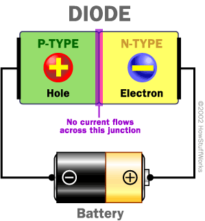
Diode

Transistor

Thyristor

Insulated Gate Bipolar Transistor (IGBT)

Power Electronics Applications
Application examples power electronics for controlling the AC voltage, controlling dimers, as well as applications for the IGBT inverter.
1. Controlling Voltage AC
on free phase control method provides an on AC control system. AC line voltage controller is used in order to toggle between the rms value of the AC voltage supplied to the load and also uses Thyristor as a switch. Applications of these equipments among others, are:
Control of heating equipment
290 lighting control
Induction motor speed controller
2. Control Dimer
Control can be done while wearing this method is limited only to the first phase of sheer burden. For a larger load subsequently be continued wearing 3-phase system, whether it is a half-wave alone or in a full-wave (bridge circuit).
3. Application to the IGBT Converter
Cycloconverter circuit when an AC voltage 3 phase DC voltage is rectified so by 6 pieces Diode. Next 9 pieces IGBT build configurations that will create 3 phase AC voltage as well as frequency and voltage that can be set, by controlling the ON time in PWM generator.
X . III Power Electronics Applications In Everyday Life
Power Electronics Applications In Everyday Life - power electronics or power electronics is electronics EAM application contained in electrical equipment settings that have great power by changing the electrical parameters such as voltage, current, up to power.
The intended application is a circuit that use electronic devices, especially semiconductor that has a function as a switch or switching to make the adjustment. The trick is to change the type of source of AC to AC, AC to DC, DC to DC and DC to AC.
Power Electronics Applications
AC to DC converter (rectifier)
AC to DC converter is a circuit used to convert AC current into DC current, which can be controlled or regulated. The converter functions must rectify the electrical current into alternating current direction. Suppose an electrical energy AC 220 V / 50 Hz derived passes to 12 VAC transformer, then rectified by the diode into DC 12V.
AC to AC converter (Cyclo converter or Matrix)
AC to AC converter or commonly referred to Cyclo converter / Matrix is a circuit that can convert AC current to AC current remains that can be controlled or regulated. AC to AC converter has the function of converting electrical energy of alternating current into alternating current with the voltage and frequency to another. Eg AC 220 V with a frequency of 50 Hz is converted into electrical AC 110 V with a frequency of 100 Hz.
DC to DC converter (Chopper)
DC to DC converter is a circuit that can convert DC currents remain a DC current that can be controlled or regulated. Its function is to convert the direct current into different magnitudes. For example a 15V DC power is converted into DC power of 5V.
DC to AC converter ( inverter )
DC to AC converter or inverter is commonly called a circuit can change the fixed DC current to AC current that can be controlled or regulated. DC to AC converter has the function to change the direction of electricity into alternating electrical voltage and frequency can be set. Eg 12 V DC power from the accumulator is converted into electricity 220V AC voltage with a frequency of 50 Hz.
1. Diode or Diode
Probably most of you are already familiar with the electronic components of this one. Yes, the diode is one of the basic electronic components are also included in the category of active electronic components. This component has a function as a diode rectifier in an electronic circuit. Diodes also include one type of power electronics components are most common.
2. Transistor
Transistors are basic electronic components are also entered into the ranks of active electronic components. Components that have the function as an amplifier and switch also includes one type of power electronics components that are often encountered in various kinds of electronic circuits.
3. IGBT (Insulated Gate Bipolar Transistor)
IGBT is actually one type of transistor. Insulated Gate Bipolar Transistor is a combination of BJT and MOSFET. Many people refer to this component as a bi-polar transistor that has a function as a switch in an electronic circuit.
4. Thyristor
The thyristor is a power electronics component made of semiconductor materials. Components of this one also has a function as a switch or switch in an electronic circuit.
X . IIII POWER Electronic for education
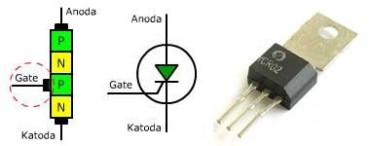
Power Electronics is one area of the study and discusses electronics applications related to electric power equipment is large enough. A wide variety of equipment and real applications in industries that use power source has enormous power capacity such as electric motors, heating, cooling, fun, compressors, pumps, conveyors and other applications.thyristorThyristor is an electronic device that consists of four layers of semiconductor PNPN and has three joint-pn. The thyristor has three terminals, namely the anode, cathode, and gate (gate). Thyristor controlled rectifier is also called, as it has a gate that serves to control the flow.How it Works Thyristor:
Thyristor this will work or deliver electric current from the anode to the cathode when at the gate by currents towards the cathode, so the gate should be given a positive voltage to the cathode. Giving this voltage to ignite the thyristor, and when ignited thyristor will still deliver. Thyristor will be interrupted if the current through the anode to the cathode becomes small or the thyristor gate is connected to ground.Various Thyristor:
Phase-control thyristor (SCR)
Fast-switching thyristor (SCR)
Gate-turn-off thyristor (GTO)
Bidirectional triode thyristor (TRIAC)
Reverse-conducting thyristor (RCT)
Static Induction Thyristor (SITH)
Light-activated silicon-controlled rectifier (LASCR)
FET-controlled thyristor (FET-CTH)
MOS-controlled thyristor (MCT)
Requirements that cause Thyristor drain current (Turned On):
Hot. If the thyristor temperature is high enough, there will be an increase in the number of pairs of electrons - hole, so that the leakage current increases. This will lead to an increase in α1 and α2 increased. Because the regenerative action (α1 + α2) will be heading to the unit value and the thyristor may be on. This can lead to thermal runaway and usually avoided.
Light. If the light allowed the thyristor connection, the pair electron - hole will be increased; and thyristor may be on. How this is done by letting the light of the silicon wafer of the thyristor.
High voltage. If the forward voltage anode to the cathode is greater than the forward breakdown voltage VBO, a leakage current is generated is enough to make the thyristor on. This method is destructive and should be avoided.
Dv / dt. If the rate of rise of voltage anode - cathode is sufficiently high, the charging capacitor connection might be enough to make the thyristor on. Values higher charging currents can damage the thyristors; and devais be protected against dv / dt is high. Manufacturing thyristor maker will determine how large dv / dt can be handled by a thyristor.
Flow gate. If a thyristor given a forward bias voltage, gate current injection by applying a positive gate between the gate terminal and the cathode will be make thyristor on. When the current enhanced gate, a forward blocking voltage will decrease.
How Thyristor Turned Off:How to make the SCR becomes OFF by lowering the anode-cathode voltage to zero. Because this is the SCR or thyristor is generally not suitable for DC applications. This component is more widely used for the application of AC voltage, because the SCR can be OFF when the AC voltage waveform is at zero.Commutation itself (line commutated):Commutation itself (line commutated), natural technique that is used, because the working voltage used is ac. At any one period of ac voltage will pass twice the point of zero volts is 0 degrees and 180 degrees. Once the voltage passes through the points (trigger) is then automatically triac will undergo commutation. This is one advantage when using triac at working voltage ac.Forced commutation (forced commutated):Forced commutation (Forced commutation), commutation is used for applications working voltage is dc (linear), because the triac once triggered will pass dc current continuously. To condition the occurrence of zero voltage on the triac is needed to set a special circuit containing an array of capacitors and inductors even use more than one fruit triac.The difference between Thyristor and Triac:Triac different from the thyristor, triac which can control the flow in two directions. Two Thyristor Triac is connected in parallel in contrast to the gate terminal together. Unlike the thyristor which just missed the voltage of positive polarity, but Triac can be triggered by positive and negative polarity voltage, and can be turned on by using an alternating voltage at the Gate. Triac is widely used in the circuit and switching control. Triac is only activated when the polarity of the anode and the cathode is more positive than their gate given a positive polarity, and vice versa. Triac can conductive character in two directions. In this case can be considered as two thyristors connected in antiparallel with the gate connection. Because the triac is a bidirectional components, the terminal can not in absolute at anode / cathode.I. Phase-Control Thyristor (phase control thyristor)The thyristor mode generally operates at line-frequency and off by natural commutation. Turn off time, TQ, is in the order of 50 to 100 ms. These devices are very suitable for low speed switching applications and is commonly known as thyristor converters. Because it is actually a thyristor controlled devices are made of silicon, consequently thyristor this type are known as silicon-controlled rectifier (SCR). The voltage is turned on, varies around 1:15 devais V to 600 V and 2.5 V for device 4000V; and for thyristor 5500A, 1200V, approximately 1,25V. Gate amplifier produces common dynamic characteristics dv / dt of 1000V / ms and di / dt of 500 A / ms and simplify circuit design by reducing or minimizing the inductor limiting di / dt and protection circuit dv / dt.
2. Fast-Switching ThyristorUsually thyristor is used in the application of technology switching speed with force-communication (eg. Thyristor this type have time turn off fast, generally in the region of 5 to 50 ms depending on local voltage. The voltage falls forward on the circumstances on varies roughly as an inverse function of the turn-off time TQ. this thyristor mode is also known as thyiristor inversion.This thyristor has a dv / dt high usually 1000V / ms and di / dt of 1000V / ms. Turn-off fast and di / dt is high will be very important to reduce the size and weight of the reactive components and for commutating circuit. On state voltage of the thyristor 2200A, 1800 V is typically around 1.7 V. The thyristor inverter with reverse blocking capability is very limited, approximately 10 V, and the turn-off time is very fast, about 3 to 5 ms, commonly known as Asymmetrical Thyristor (ASCR).
3. Gate-Turn-Off ThyristorGate-Turn-Off Thyristor like SCR can be turned on by providing a positive gate signal. However GTO can be turned off by giving a negative gate signal. GTO is also a device latching and can be built with current and voltage rating similar to SCR, GTO is turned on by providing positive short pulse signal at the gate and turned off by giving a negative short pulse signal at the gate. GTO that has several advantages over SCR:a. Elimination of components commutating the forced-commutation, resulting in reduced cost, weight and volume.b. Reduction of acoustic and electromagnetic due to the loss of commutation chokes.c. Turn-off fast, enabling high switching frequencyd. Improving the efficiency of the converter.In low power applications, the GTO has advantages over the bipolar transistor is:
(1) The ability of blocking a higher voltage;(2) The ratio of the peak current that can be controlled with the average current higher;(3) The ratio of the peak surge current for average current is high, generally 10: 1;(4) Strengthening the state on high (anode current / current gate), generally 600; and(5) The duration of the gate signal pulse. In the surge condition, GTO will likely go into deeper saturation for their regenerative action. Meanwhile, bipolar transistor tends to be out of the state of saturation.GTO has a lower reinforcement during turn-off, generally six, and the negative current pulses require relatively large for a turn-off. When the voltage falls on relatively larger than SCR. The voltage is turned on for an average of 550 GTO A, 1200 V peak magnitude of 3.4 V. Controllable on state ITGO is the peak value on the circumstances that can be turned off by the control gate, off-state voltage is given immediately after the turn-off and dv / dt only will be limited by capacitance of snubber. So GTO is turned off, the load current IL that flows through and fill the snubber capacitor, determine dv / dt is the case with Cs is a snubber capacitance.
4. Bidirectional Triode Thyristor (TRIAC)TRIAC can be conductive in two directions and are typically used to control ac phase (eg ac voltage controller). It can be considered two thyristors connected in anti parallel with the gate connection.
Because the TRIAC is a bidirectional devais, the terminal can not be determined as the anode / cathode. If the positive terminal of the terminal MT1 MT2, TRIAC can be turned off by giving a positive gate signal between the gate G and MT1. If the negative terminal MT1 MT2, the TRIAC will be turned on by giving a negative pulse signal between the gate G and terminal MT1. No need to have both positive and negative gate signal and TRIAC can be powered either by the gate signal is positive or negative.
5. Reverse Conducting Thyristor (RCT)In many chopper or inverter circuit, anti-parallel diode is connected along SCR to allow reverse current flow due to the inductive load and to improve the current performance of the circuit turn-off commutation. Reverse voltage blocking diode is cut off from the SCR to -1 or 2 V at a steady state. But in a transient state, the reverse voltage can be increased up to 30 V for the voltage induced in the circuit due to the stray inductance in device.An RCT can be seen as a compromise between the characteristics and needs of the circuit device RCT can be considered as a thyristor with built-in anti parallel diode. RCT also known as Asymmetrical thyristor (ASCR). Forward blocking voltage ranging from 400 up to 2000V and current rating moves up to 500A. Reverse blocking voltage is typically around 30 to 40 V. Since the ratio of the forward current through the thyristor against reverse current of diode fixed to a devais, its application is limited by the particular design.
6. Static Induction ThyristorCharacteristics of SITH similar to the characteristics of the MOSFET. SITH is usually turned on by providing a positive gate voltage as usual thyristors on and off by giving a negative voltage on the gate. SITH is device with minority carriers. Consequently SITH has a resistance / voltage drop on the low state and can be made with a voltage rating and a higher current.
SITH has a high switching speed with the ability dv / dt and di / dt is high. on Switching time on the order of 1 to 6 ms. voltage rating can reach 2500 V and the current rating is limited to 500 A. these devices are very sensitive to the production process, a small disturbance in the production process will produce large changes in device Characteristics.
7. Light Activated Silicon Controlled Rectifier (L A S C R)
These devices turned on to provide light radiation directly to a silicon wafer. Hole electron pairs are formed during the radiation process will generate a current trigger on the influence of electric fields. Gate structure is designed to generate enough gate sensitivity to triggering with practical light sources. L A S C R used for current consumption and high voltages. (Example for high voltage dc transmission and static reactive power compensation or reactive volt amperes). LASCR provide full electrical isolation between the light source and device pen trigger switching of power converters., With high-potential floating up to several kilo volts. Voltage rating of LASCR can be as high as 4 kV, 1500 A with pen trigger light power less than 100 mW. di / dt common is 250 A / m s and dv / dt can be as high as 2000 V / m s.
8. FET Controlled ThyristorDevice FET-CHT combine MOSFET and Thyristor in parallel. If a certain voltage supplied to the gate of the MOSFET, typically 3 V, current pen trigger of thyristor will be raised internally. FET - CHT has high-speed swtching, di / dt and dv / dt is high.These devices can be turned like a conventional thyristor, but can be turned off by the control gate. It is indispensable in applications that optical firing is used to generate electrical isolation between the input or control signals and power switching device.
9. The thyristor controled MOS-
MOS-Controlled Thyristor (MCT) combines nature - the regenerative properties of the thyristor and the MOS gate structure. MCT can operate as device controlled by the gate if the current is less than the maximum current that can be controlled. MCT effort to be made off of the current exceeds the value that would result in damage device . For high current values MCT thyristor to be switched off as usual. The pulse width of the gate is not critical for smaller devices whose currents. For large current, turn off the width of the pulse should be larger. Further, the maximum gate current will flow during turn - off. In many applications, including inverter and chopper, gate pulses continuously during the period of on / off is necessary to avoid confusion.An MCT has:1. The forward voltage drop for a state on a low2. Time turn off fast (0.4 m s) and a fast time is usually 1:25 m s for MCT 300A, 500V3. Low switching power dissipation4. Ability blocking voltage low5. The high input impedance of the gate, which will simplify the drive circuitMCT can effectively be installed parallel to the process of switching large currents with only modest changes to the rating current rating device slice there. MCT can not be mobilized with a pulse transformer can be continuous if necessary to avoid confusion.
CONVERTER
Converter is a tool to convert electrical power from one form to another electrical power.AC-DC converter (rectifier):
A circuit that converts AC voltage into DC voltage that can be controlled / regulated. Its function electric rectify alternating current into direct current electricity. Energy flows from the AC power system is one way to DC systems. Example: Power AC 220 V / 50 Hz derived passed into 12VAC transformer and then rectified by the diode into a DC voltage of 12V.Diode rectifier circuit change ac voltage to dc voltage is fixed. The input voltage to the rectifier can be either single phase or three phase and are shown in the following figure:1. The half-wave rectifier, single phase
2. The full-wave rectifier, three phase
3. The half-wave rectifier, three phase
AC-AC converter (Cycl oconverter):A circuit that can convert AC voltage remains an AC voltage that can be controlled / regulated. Its function converts electrical energy of alternating current with a certain frequency and voltage into an alternating current with the voltage and frequency of the other. There are two types of AC converters, namely:• AC voltage regulator (a voltage change, constant frequency)• cyclo converter (voltage and frequency can be adjusted).Example: AC voltage of 220 V and a frequency of 50 Hz into AC voltage of 110 V and a new frequency of 100 Hz.
DC-DC converter (Chopper):A circuit used to convert the DC voltage source remains a DC voltage source that can be controlled / regulated. Direct current power is converted into direct current as well but with different magnitudes. Example: Power DC 15V with electronic components is converted into DC power of 5V.
DC-AC converter ( inverter ):A circuit used to convert the DC voltage source remains a source of AC voltage that can be controlled / regulated. Its function is to change the direct current electricity into alternating current electricity at a voltage and frequency can be set. Example: Power DC 12 V from accumulator with inverter device is converted into electrical voltage AC 220V, 50 Hz frequency.
In the modern era, as now, the development of the electricity needs of the community extends to almost all sectors. Starting from households, public infrastructure, industrial, offices, transportation, and even shopping. Increased demand for electricity must be balanced by an increase in electrical power source, in addition to increased efficiency in the load can also help the effectiveness of the use of electricity itself. In this case the inverter as a power electronics device has an important role in these two cases. First as a provider of electrical power source, the inverter is able to play a role in converting electricity derived from renewable sources power energy into electricity that can be used by end users. Secondly, the inverter is also widely used in electrical devices to optimize the efficiency of such devices, up to utilization of power resources can be optimized.
Some time ago said inverter may still lay ears of the community. However, with seiringnya time, said inverter start prevalent and often heard. Characterized by frequent appearance of the word in advertising some product Inverter household electrical appliances glass screen, such as AC Inverter, inverter refrigerator and so forth. In the ads mentioned that by using the inverter will be found significant electrical power saving compared to previous products that still use conventional systems.
Whereas in the industrial world, Inverter has long been used for various applications, such as conveyor drive motor, drive motor compressor, as UPS and many more. In the field of mass transportation, the inverter is used as propulsion systems or main driving electric trains replaced the technology Rheostatic outdated and wasteful of energy, besides Static inverters are also used to distribute electrical installation replaces the motor-generator sets that simplify treatment in the absence of moving parts inside the inverter. In the world of renewable energy resources, an inverter occupy an important position in bridging the presence of electrical energy from renewable resources by the end user. Because in general the electrical energy from renewable resources can not be used directly by end users. For example, the electrical energy generated by solar cells is a direct voltage (DC) can not directly be distributed and used by the end user loads which generally has a specification input voltage alternating (AC). Another example is the source of wind power, where the wind is not continuous may interfere with the existence of electricity in the network, so it needs special handling so that this energy source can be used, for example, to be stored for all energy storage systems such as batteries, and then from the battery is converted by an inverter streamed to a network.
equirements as inverter products in general, among others:
Endurance test, inverter weighed 50% load for at least 5 hours without any damage and irregularities performance.
Overload test, when the inverter successfully passed the test of excessive load up to 140% for 1 minute.
Ouput THD of less than 4%
ELECTRONIC POWER
Equipment and applications in industries that use large capacity electrical energy such as electric motors, compressors, pumps, conveyor, fan, cooling, heating and others require setting. Power electronics are popular for a variety of conventional arrangements can not fulfill the needs of the industry. Conventional arrangement raises the losses were quite large and are not effective and so we need better regulation mechanism is by using electronic devices.
Power electronics is the science that studies of electronics technology for the control and regulation of electric power equipment major strong currents {her} by way of conversion of current, voltage and power
Power Electronics covers and connects the various fields of science that underlies the development of power electronics, these sciences is the science of electronics, the science of electricity, control science and computer science.
To be able to master the Power Electronics 4 system should at least understand that Electronic Systems, Electrical Power Systems, Control Systems and Computer Systems.
1. Electronic System.Electronic systems is the science which contains the basic applications of basic electronics, which deals with semiconductors and other components in electronic equipment. To deepen the understanding of power electronics material digital or analog electronic circuits.
2. Electric Power System.The electrical power system is the science which deals with the amount of electric power in the electronic equipment, whether it is generated or required. Object or a central goal of power electronics applications are electrical equipment and systems that have the power {} electrical voltages and currents are quite large. Therefore, to better understand the power electronics need a good understanding of the power system.
3. Control System.The control system is the science which deals with the ability to control or manipulate or manipulate the power generated by electronic equipment. Usually needed for controlling industrial applications such as control panels, electrical machinery control, pressure control, speed control motors and others. Because it takes a good understanding of the techniques and systems control a wide range of equipment that is in use in the industry.
4. Computer Systems.
The computer system is the science which deals in computer control. Most current industrial applications have been integrated with the computer system used to control equipment remotely industry and the results can be monitored. Because the power electronics required to master the control of computer systems.
Broadly speaking, the power electronics is divided into two parts, namely the power circuit and control circuits.1. Power is a series circuit consisting of diode components, Thyristor and Power Transistor2. The control circuit is a circuit consisting of diodes, transistors and ICs.
X . IIIII Power circuit example of the working principle of the control circuit can be seen below;

One of the well publicized benefits of an EV is regenerative braking. Regen braking is common on nearly all vehicles now, yet few people seem to realize what happens. The following paragraph is an attempt to explain how it works.
In the circuit shown above is an output pair of MOSFETs Metal Oxide Semiconducting Field Effect Transistors), with the motor being driven. The output from the controller is a pure d.c. voltage. The motor will generate a back e.m.f. which is proportional to its speed of rotation. At zero load, or no acceleration, this back e.m.f. will rise to be equal to the output from the controller.
The MOSFET is a bi-directional switch which conducts resistively (when it is turned on) for both directions of current. So consider the situation when the current is zero and the controller's output is now reduced. The motor's back e.m.f. is now higher than the controller's output voltage - so the motor will try and feed current back into the controller. If it succeeds in so doing the motor will be braked - we will have regenerative braking.
This type of circuit (where hi-side is turned on when the low-side is off) is capable of sourcing current or sinking it. The way this works is that the reversed motor current is now a forward current to the flywheel MOSFET so when this is on it shorts out the motor - whose braking current rises during this period (arrow B, reversed). The Flywheel MOSFET now turns off, but this current must keep flowing - because of the motor's inductance. So it flows as reverse current through the drive MOSFET, recharging the battery as is does so. The extra voltage for this is derived from the energy stored in the motor's inductance. The process of switching from drive to braking is entirely automatic. Moreover it is done entirely by the motor's speed exceeding the drive voltage and without any change of state or switching within the controller. The regen braking is, if you like, a by-product of the design of the controller and almost a complete accident.
If the vehicle is driven down too steep a hill (or the demand speed is suddenly reduced so that very hard braking results) the current generated by the motor could exceed that which the MOSFETs can safely handle. Since this would blow the MOSFETs it must be protected against so all controllers that give regenerative braking are also fitted with a current limit to stop such failure.
In Hybrid Electric Vehicles this problem becomes even more complex because of the unused current from the auxiliary power source. Since the drive motors are not drawing current from the auxiliary power source, that current still must have some place to go. The motor controller should monitor and take into account the excess current from the auxiliary power source, so that in certain situations where too much current is present with regen and APU operating, the regen MOSFET must also be turned off. to protect the motor controller.
In early version of electric vehicles with DC motors, a simple variable resistor type controller governed the acceleration and speed of the vehicle. Full current and power was drawn from the battery all of the time. At lower speeds, when little power was needed, high resistance was used to reduce the current to the motor. This resulted in a large percentage of the battery's energy being wasted as heat dissipated by the resistor. Modern controllers adjust speed and acceleration by and electronic process called pulse width modulation(PWM). Switching devices such as IGBT's(very fast, high current rated transistors) rapidly interrupt, turning on or off as needed, the flow of electricity to the motors. High power is achieved when the intervals(time between pulses) are very short. By increasing the time between pulses, the current is limited.

The wheel motor shown above is manufactured by Technologies M4.
As mentioned above, one of the more interesting designs for motors is to integrate the motor directly into the wheel. These are called wheel motors and may very well become the norm someday as they remove a tremendous amount of mechanical devices from the vehicle by providing propulsion to the wheel...in the wheel!
The motor-wheel assembly is an elegant integration of an electric motor and other components into a package that fits inside a regular-size tire.
The motor-wheel assembly consists of a highly efficient electric motor, a Motor-Wheel Slave Controller (MWSC) including power and control electronics, a brake, wheel bearings, a steerable front suspension interface and a heat sink embedded in the stator. The configuration of the 3-phase synchronous motor consists of a central stator which supports the windings and the inverter, surrounded by an external rotor which supports the permanent magnets.
The wheel is directly mounted on the rotor for direct transmission of torque and enhanced freewheeling. The motor assembly is liquid-cooled to sustain high continuous power demands.
Bus manufacturers will appreciate the packaging advantages and interchangeability of the motor-wheel rear axle, which easily fits within existing wheel housings. The axle deep-offset cross member enables a wider floor aisle area in the low-floor configuration.
Selecting a motor for use in an EV involves many variables. No single type of motor can be considered as the best. When an EV is being designed, questioned must be answered before selecting a specific type of motor. How much power do you need, do you need variable speeds, what is the operating voltage of the battery system, what kind of torque do you need and at what speed, how much physical space can the motor occupy, how much can it cost, what type of environment will the motor be operating in? Once these questions are answer, you can make your motor selection. Once the motor has been identified, a control system must be designed to make the motor functional.
Control Systems
| The most complex and important system in an EV is the control system. The control system is responsible for governing the operation of the electric vehicle. The control system receives inputs from the operator, Controllerfeedback signals from the motor controller and motor and also feedback signals from other systems within the EV. The speed at which the control system must receive data from other systems, process the data in an algorithm and output a response to the given conditions must be accomplished in milli-seconds. This requires the control system to have a microprocessor, just like a computer, to accomplish its tasks. Though no two control systems are identical, most of the feedback signals are similar. The table below lists common components of a control system and the feedback signals that are sent to the microprocessor. | |||||||||||||||||||||||||||
 A motor controller. |
|
||||||||||||||||||||||||||
In some advanced control systems, it is possible to limit the amount of current that flows to the motor, based on a switch selection. This allows the operator to adjust to a driving style that fits a particular situation. For instance, if a driver needs a certain range(in miles) from a single charge, the range selection can be set so that the microprocessor will limit the amount of output current from the motor controllers to a preset limit. If the preset limit is 100 amps, the microprocessor will not allow any current above this limit to flow to the motors. In this mode, acceleration ability is sacrificed for range. If the driver is in an area where the vehicle must climb steep grades, the range selector can be set so that the maximum current capability of the motor controller and motor can be used. The range selection feature is a valuable feature that adds to the efficiency of the motor controller. The ultimate goal of a control system is to maximize the energy stored within the traction battery and to prevent unsafe conditions from occurring within the electric vehicle.
Battery Systems
 An electric vehicle's battery, with cells visible. |
An electric vehicle's battery defines the range, acceleration ability and recharge
time for the vehicle. Because the battery contains the energy to fuel an electric
vehicle, and because today's batteries do not provide electric vehicles with the same
range potential as ICE vehicles, batteries, and alternative options such as flywheels
and ultra capacitors, are the most heavily studied areas in electric Battery cellvehicle
technology. |
||
| A battery cell normally consists of the 4 principal components shown at the left. A cell contains a positive and negative electrode, electrolyte, and a separator. The positive electrode receives electrons from the external circuit when the cell is discharged. The negative electrode donates electrons to the external circuit as the cell discharges. The electrolyte provides a mechanism for charge to flow between positive and negative electrodes. The separator electrically isolates the positive and negative electrodes. |
 | ||

Performance of Vehicle Battery Systems
Each specific type of battery has characteristics which make it either more or less desirable to use in a specific application. Cost is always a major factor and the NiMH battery tops the list in price with flooded lead acid batteries being the most inexpensive. What is lost in the cost translation is the fact that NiMH batteries yield nearly twice the performance (energy density per weight of the battery) than do conventional lead acid batteries. Another factor that must be considered when making a battery comparison is the recharge time. Lead acid batteries require a very long recharge period, as long as 6 to 8 hours. Lead acid batteries, because of their chemical makeup, cannot sustain high current or voltage continuously during charge. The lead plates within the batteries heat rapidly and cool very slowly. Too much heat results in a condition known as "gassing" where hydrogen gas is released from the battery's vent cap. Over time, gassing reduces the effectiveness of the battery and also increases the need for battery maintenance. Batteries such as NiCad and NiMH are not as susceptible to heat and can be recharged very quickly, allowing for high current or high voltage charges which can bring the battery from a 20% state of charge to an 80% state of charge in as quick as 20 minutes.
|
Battery Type
|
Energy Density Whr/kg
|
Power Density W/kg
|
Life Cycles Per Battery
|
Cost on scale of 1 to 10
|
| Current Lead Acid |
35
|
150 |
500
|
1
|
| Advanced Lead Acid |
48
|
150
|
800
|
3
|
| GM Ovonic NiMH |
70
|
220
|
>600
|
8
|
| SAFT NiMH |
70
|
150
|
1,500
|
8
|
| SAFT lithium ion |
120
|
230
|
600
|
9
|
| Lithium polymer |
150
|
350
|
<600
|
10
|
| Zebra sodium-nickel chloride |
86
|
150
|
<1000
|
4
|
| Impact on Vehicle performance |
Range
|
Acceleration
|
Life Cycle Cost, Replacement Cost
|
Initial Cost, Replacement Cost
|
New technology battery systems are also driven by a microprocessor. The microprocessor receives data from sensors within the battery pack. Temperature, current output, battery voltage and fault detection are all fed back to the microprocessor which can then calculate how much energy is remaining in the battery as well as how much has been consumed. Monitoring the temperature and the resistance to the vehicle's ground protects both the battery pack and the passengers from danger.
Battery configurations also vary greatly depending on the vehicle and the desired redundancy of the system. Battery packs can be tied together in one long series circuit so that the total pack voltage is the sum of all the cells in the series. Other systems use multiple packs that are of equal voltage and parallel the multiple packs. This provides redundancy to the system. If a cell goes bad in a single pack, the battery management system can disable the output from that pack and the vehicle can continue to be driven off of the remaining battery packs. The vehicle will lose the energy from the faulty pack and range will be affected.
 |
Shown to the left is a battery pack consisting of 27 individual 2 volt cells,
in a series circuit configuration to form a pack with a voltage of 54 volts. |

Specific energy is energy density as a function of time measured in watt-hours per unit mass. Specific energy is important because it affects the number of batteries necessary in a particular application, and in turn the mass or weight of the batteries that a vehicle needs to carry on-board to end up with a certain electric-only range. It is the most important factor for EVs because it determines their total range, but not as critical for HEVs which carry the majority of their energy in the form of a gaseous or liquid fuel. Instead, for HEVs, a battery's specific power becomes the critical parameter in selecting a battery.
 Since HEVs utilize two different energy sources, energy demands from the batteries
are much less than in EVs. Because hybrids normally only depend on the electrical
energy stored on-board to provide power for acceleration and hill climbing, batteries
are sought that have a high specific power rating and less mass. Specific power, is
power per unit mass, so the ability of the battery to enable high current draws for
short durations with less weight is the desired goal for HEVs. Shown at right is a
chart which compares specific power between battery types. No information was available
for the lithium batteries at this time.
Since HEVs utilize two different energy sources, energy demands from the batteries
are much less than in EVs. Because hybrids normally only depend on the electrical
energy stored on-board to provide power for acceleration and hill climbing, batteries
are sought that have a high specific power rating and less mass. Specific power, is
power per unit mass, so the ability of the battery to enable high current draws for
short durations with less weight is the desired goal for HEVs. Shown at right is a
chart which compares specific power between battery types. No information was available
for the lithium batteries at this time.
 Battery chargers replenish the energy used by an electric vehicle much like a gasoline
pump refills a gas tank. One significant difference is that an electric vehicle operator
can fully charge the vehicle overnight, at home, rather than refueling at a gasoline
station. The battery charger is a device which converts the alternating current distributed
by electric utilities to the direct current needed to recharge the battery.
Battery chargers replenish the energy used by an electric vehicle much like a gasoline
pump refills a gas tank. One significant difference is that an electric vehicle operator
can fully charge the vehicle overnight, at home, rather than refueling at a gasoline
station. The battery charger is a device which converts the alternating current distributed
by electric utilities to the direct current needed to recharge the battery.
Battery Memory
It is often heard that batteries have memory. When "memory" is talked about in the same sentence with batteries, it means a battery has failed to produce it's stated capacity. If a battery has a stated capacity of 100 amp-hours, and the cutoff voltage is consistently reached when only 80% or 80 amp-hours has been consumed after having been charged it is often referred to as the memory effect. There are many opinions as to whether or not batteries have memory. The use of the term "memory" to describe the loss of capacity is likely the source of the confusion. A battery's performance can be consistently poor, having a discharge capacity within 2% to 3% during each discharge cycle. But batteries do not get that way from "memory". They are several different causes of this poor performance, and generally it is the battery's caretaker who is responsible for this effect.
Some of the more common causes of performance problems that are attributed to the "memory" effect are;
1. Improper charging, i.e., consistently overcharging or undercharging
2. Exceeding battery temperature thresholds during charging or discharging
So what has happened to the battery that is experiencing a "memory" effect? Because of the different types of batteries and chemicals involved, there is no single generic term that can be applied that describes what causes the poor performance in all batteries. However, what is known is that high temperatures alter the molecular structures of the chemicals involved, which can lead to a higher internal resistance within the battery which leads to voltage depression. Undercharging can lead to a buildup of lead sulfate on the plates of lead-acid batteries which also increases the internal resistance of the battery because currents become constricted and cannot flow through the full surface area of the plates. Overcharging can have the same effect that high temperature has, altering the crystal structures of the chemicals within the battery.
Can the battery's "memory" be erased? In most cases the answer is "yes". By proper execution of several charge/discharge cycles, the memory effect can be destroyed and the battery capacity will return to it's original value. In some cases, however, if a battery has been poorly maintained for an extended period of time(months), it is possible that permanent damage has occurred and the life and capacity of the battery is defined and cannot be corrected.
Types of Charging
There are a number of different types of battery chargers based on the way they control the charging rate.
Constant Voltage
A constant voltage is applied and the current flows into the battery (the highest current occurs when the battery has been fully discharged and steps down to a low current when the battery is nearly charged.) Electronics on constant voltage charges is relatively simple, therefore, these types of chargers tend to be less expensive.

Combination Constant Current/Constant Voltage
The charge cycle starts with a high constant current until the voltage reaches a set value, then changes to a constant voltage control. This is the most sophisticated of the basic types of battery chargers and generally increases the life of a battery by reducing heat during the charging process. These chargers also tend to increase battery performance.

Pulse Charging
One of the advanced charging methods currently being evaluated eliminates the practice of requiring constant current and/or constant voltage by "pulsing" voltage. A series of very high current and voltage pulses are applied until the battery voltage reaches a set value. The major advantage of a pulse charger is the significant reduction in heat which allows the charger to operate at a high voltage rate even when the battery is almost full. Additionally, the reduction in heat results in a reduction in "lost" energy. Thus, pulse charging can significantly reduce charging time and are more energy efficient.

While there are many types of battery chargers available, the vehicle manufacturer will supply or recommend the proper charger for the batteries in the electric vehicle.
Charger Location/Coupling Options
Electric vehicle battery chargers may be onboard (in the electric vehicle) or offboard (at a fixed location). As with many options, there are advantages and disadvantages with both types. If the battery charger is onboard, the batteries can be recharged anywhere there is an electric outlet. The drawback with onboard chargers is the limitation in their power output because of size and weight restrictions dictated by the vehicle design. Offboard charges are limited in their power output only by the ability of the batteries to accept the charge. While the EV owner can shorten the time it takes to recharge the batteries with a high-power, offboard charger, the flexibility to charge at different locations is restricted.

Charging Methods
There are two basic coupling methods used to complete the connection between the utility
power grid, the battery charger, and the vehicle connector. The first is the traditional
plug (called conductive coupling). With this connection, the EV operator plugs his
vehicle into the appropriate outlet (i.e. 110 or 220 volts) to begin charging. This
type of coupling can be used with the charger in the car (onboard) or out of the car
(offboard).
The second type of coupling is called inductive coupling. This type of coupling uses a paddle which fits into a socket on the car. Rather than transferring the power by a direct wire connection, power is transferred by induction, which is a magnetic coupling between the windings of two separate coils, one in the paddle, the other mounted in the vehicle.
Inductive Charging
 The inductive charger has no direct electrical connection to the vehicle. A weatherproof
paddle transfers power to the vehicle’s charge port via magnetic field . The Delco
off-vehicle chargers provides a safe and easy-to-use system for EV charging. Inserting
the charge coupler is all that is required to initiate charging. Charging can be terminated
at any time by removing the coupler. Bi-directional communication and built-in diagnostics
ensure a safe connection and prevent the vehicle from being driven while connected.
The inductive charger has no direct electrical connection to the vehicle. A weatherproof
paddle transfers power to the vehicle’s charge port via magnetic field . The Delco
off-vehicle chargers provides a safe and easy-to-use system for EV charging. Inserting
the charge coupler is all that is required to initiate charging. Charging can be terminated
at any time by removing the coupler. Bi-directional communication and built-in diagnostics
ensure a safe connection and prevent the vehicle from being driven while connected.
Conductive Charging
With a conductive charger, energy is transferred to the vehicle via metal-to-metal contact. A connector, such as the AVCON (left), safely performs the link between a power supply and the vehicle’s charge port.
Charge Levels
Chargers are also classified by the level of power they can provide to the battery pack:
Level 1 - Common household type of circuit, rated to 120 volts/AC and rated to 15 amps.
Level one chargers use the standard household 3-prong connection and they are usually considered portable equipment.
Level 2 - Permanently wired electric vehicle supply equipment used specially for electric vehicle charging and it is rated up to 240 volts/AC, up to 60 amps, and up to 14.4 kilowatts.
Level 3 - Permanently wired electric vehicle supply equipment used specially for electric vehicle charging and it is rated greater than 14.4 kilowatts. Fast chargers are rated as Level 3 chargers. However, not all Level 3 chargers are considered as fast chargers. This depends on the size of the battery pack to be charged and how much time is required to charge the battery pack. A charger can be considered a fast charger if it is capable of charging an average electric vehicle battery pack in 30 minutes or less.
Battery Management
 With so many differences in chargers and charging methods, there existed a need to
monitor the status of the batteries being charged and discharged. Battery Management
Systems (BMS) have been developed which are microprocessor controlled allowing charge
algorithms to be programmed into the system for virtually all the different battery
types. These systems monitor the energy consumed by the vehicle while being driven,
as well as temperature, individual cell voltages and total pack voltage. The same
process is monitored in reverse during charging creating a safety net in the event
of problems with a single cell within the battery pack.
With so many differences in chargers and charging methods, there existed a need to
monitor the status of the batteries being charged and discharged. Battery Management
Systems (BMS) have been developed which are microprocessor controlled allowing charge
algorithms to be programmed into the system for virtually all the different battery
types. These systems monitor the energy consumed by the vehicle while being driven,
as well as temperature, individual cell voltages and total pack voltage. The same
process is monitored in reverse during charging creating a safety net in the event
of problems with a single cell within the battery pack.
With existing electric vehicles and battery chargers, it usually takes from several hours to overnight to recharge an electric vehicle battery pack. The time required to recharge electric vehicle batteries depends on the total amount of energy that can be stored in the battery pack, and the voltage and current (i.e., power) available from the battery charger.
New developments in battery recharging decreases the time required to recharge electric vehicle batteries to as little as 10-15 minutes. For example, pulse battery chargers have demonstrated that the EV battery pack can be recharged in under 20 minutes without damaging it. When this technology is fully deployed, electric charging stations, similar to gas stations, will allow the electric vehicle operator to quickly recharge the battery pack.
This new charger technology, coupled with advanced batteries with a range of 200 miles between recharging, will allow the electric vehicle operator the same freedom of the road currently enjoyed by today's operators of gasoline-powered vehicles.
Accessories (Power windows, heating, air, power steering, etc.)
An EV maintains the same accessory functions as a vehicle utilizing an internal combustion engine. These accessories include radios, lights, heating and air conditioning, power steering, and for larger vehicles such as trucks and buses, an air system. However, the manner in which these devices obtain power is very different. A combustion engine is equipped with a generator for 12 volt power. The engine cooling system is the heat source for the vehicle. Air conditioning and power steering are accomplished using a belt and pulley system which interfaces with a pump for the power steering and a compressor for the air conditioning. Since electric vehicles do not utilize an engine, alternative methods have been developed to work with EVs.
The 12 volt accessory system which supplies power to devices such as lights, radio, windshield wiper and washer system, power windows and door locks or any other electrical device on the vehicle consumes energy from the main traction battery. The accessory system does not operate at the same voltage level as the traction system(the system that provides power to the wheels), but is instead stepped down from a voltage range of 324-216 volts DC to 12 volts DC though a device called a DC to DC converter.
There are several different methods that can be used to heat an electric vehicle. One of the first methods used was known as "resistance" heating. Resistance heating is accomplished using a heat element, similar to heat elements on a stove top or in the oven. The heat element is warmed when electricity is applied, and a fan blows across the element to disperse the heat. The disadvantages of this method included safety and efficiency. Heat elements consume a large amount of energy. Other alternative methods of heating included using heaters which burned a clean fuel such as liquid propane or compressed natural gas. Cooling electric vehicles has been accomplished in the past using standard air conditioning technology similar to window mount home air conditioners. These air conditioners were effective though inefficient. Recent developments in power electronics has enabled vehicle manufacturers to place an efficient reversible heat pump, one that can cool or heat, into electric vehicles.
Power steering on an electric vehicle is accomplished by adding a single speed DC motor and a motor controller. The motor is coupled to the power steering pump through gears or a belt and pulley system. The motor controller's job is to keep the motor spinning at a constant speed under varying loads. The air system on large trucks and buses utilizes this same methodology with the DC motor turning the shaft of an air compressor. What is important to realize here is that the DC motors will only come on and stay on if the vehicle needs air or power steering. If the vehicle is stopped, power steering is not needed and the power steering motor will shut off. Whenever the air tanks are full, that motor will also shut off.
X . IIIIII Types of Chopper Circuits
In chopper circuits,
unidirectional power semiconductors are used. If these semiconductor
devices are arranged appropriately, a chopper can work in any of the
four quadrants. we can classify chopper circuits according to their
working in any of these four quadrants as type A, type B, type C,
type D and type E. Let us now take a look of these classifications and
the characteristics of various classifications.
Type A Chopper or First–Quadrant Chopper
This type of chopper is shown in the figure. It is known as first-quadrant chopper or type A chopper. When the chopper is on, v0 = VS as a result and the current flows in the direction of the load. But when the chopper is off v0 is zero but I0 continues to flow in the same direction through the freewheeling diode FD, thus average value of voltage and current say V0 and I0 will be always positive as shown in the graph.

- Chopper First Quadrant
In type A chopper the power flow will be always from source to the load. As the average voltage V0 is less than the dc input voltage Vs
Type B Chopper or Second-Quadrant Chopper

- Chopper Second Quadrant
In type B or second quadrant chopper the load must always contain a dc source E . When the chopper is on, v0 is
zero but the load voltage E drives the current through the inductor L
and the chopper, L stores the energy during the time Ton of the chopper . When the chopper is off , v0 =( E+ L . di/dt ) will be more than the source voltage Vs .
Because of this the diode D2 will be forward biased and begins
conducting and hence the power starts flowing to the source. No matter
the chopper is on or off the current I0 will be flowing out of the load and is treated negative . Since VO is positive and the current I0 is negative , the direction of power flow will be from load to source. The load voltage V0 = (E+L .di/dt ) will be more than the voltage Vs so the type B chopper is also known as a step up chopper .
Type -C chopper or Two-quadrant type-A Chopper
Type C chopper is obtained by connecting
type –A and type –B choppers in parallel. We will always get a
positive output voltage V0 as the freewheeling diode FD is
present across the load. When the chopper is on the freewheeling diode
starts conducting and the output voltage v0 will be equal to Vs . The direction of the load current i0 will be reversed. The current i0 will
be flowing towards the source and it will be positive regardless the
chopper is on or the FD conducts. The load current will be negative
if the chopper is or the diode D2 conducts. We can say the chopper and
FD operate together as type-A chopper in first quadrant. In the second
quadrant, the chopper and D2 will operate together as type –B chopper.

- Chopper Two Quadrant
The average voltage will be always
positive but the average load current might be positive or negative. The
power flow may be life the first quadrant operation ie from source to
load or from load to source like the second quadrant operation. The two
choppers should not be turned on simultaneously as the combined action
my cause a short circuit in supply lines. For regenerative braking and
motoring these type of chopper configuration is used.
Type D Chopper or Two-Quadrant Type –B Chopper

- Two Quadrant Type B chopper or D Chopper Circuit
The circuit diagram of the type D chopper is shown in the above figure. When the two choppers are on the output voltage v0 will be equal to Vs . When v0 = – Vs the two choppers will be off but both the diodes D1 and D2 will start conducting. V0 the average output voltage will be positive when the choppers turn-on the time Ton will be more than the turn off time Toff its
shown in the wave form below. As the diodes and choppers conduct
current only in one direction the direction of load current will be
always positive.

- Positive First Quadrant Operation and Negative Fourth Quadrant Operation
The power flows from source to load as the average values of both v0 and i0 is positive. From the wave form it is seen that the average value of V0 is positive thus the forth quadrant operation of type D chopper is obtained.
From the wave forms the Average value of output voltage is given by
V0= (Vs Ton-VsToff)/T = Vs.(Ton-Toff)/T
V0= (Vs Ton-VsToff)/T = Vs.(Ton-Toff)/T
Type –E chopper or the Fourth-Quadrant Chopper
Type E or the fourth quadrant chopper
consists of four semiconductor switches and four diodes arranged in
antiparallel. The 4 choppers are numbered according to which quadrant
they belong. Their operation will be in each quadrant and the
corresponding chopper only be active in its quadrant.

- E-type Chopper Circuit diagram with load emf E and E Reversed
- First Quadrant
During the first quadrant operation the
chopper CH4 will be on . Chopper CH3 will be off and CH1 will be
operated. AS the CH1 and CH4 is on the load voltage v0 will be equal to the source voltage Vs and the load current i0 will begin to flow . v0 and i0 will
be positive as the first quadrant operation is taking place. As soon as
the chopper CH1 is turned off, the positive current freewheels through
CH4 and the diode D2 . The type E chopper acts as a step- down chopper
in the first quadrant.
- Second Quadrant
In this case the chopper CH2 will be
operational and the other three are kept off. As CH2 is on negative
current will starts flowing through the inductor L . CH2 ,E and D4.
Energy is stored in the inductor L as the chopper CH2 is on. When CH2 is
off the current will be fed back to the source through the diodes D1
and D4. Here (E+L.di/dt) will be more than the source voltage Vs . In second quadrant the chopper will act as a step-up chopper as the power is fed back from load to source
- Third Quadrant
In third quadrant operation CH1 will be
kept off , CH2 will be on and CH3 is operated. For this quadrant
working the polarity of the load should be reversed. As the chopper CH3
is on, the load gets connected to the source Vs and v0 and i0 will be negative and the third quadrant operation will takes place. This chopper acts as a step-down chopper
- Fourth Quadrant
CH4 will be operated and CH1, CH2 and
CH3 will be off. When the chopper CH4 is turned on positive current
starts to flow through CH4, D2 ,E and the inductor L will store energy.
As the CH4 is turned off the current is feedback to the source through
the diodes D2 and D3 , the operation will be in fourth quadrant as the
load voltage is negative but the load current is positive. The chopper
acts as a step up chopper as the power is fed back from load to source.
X . IIIIIII Choppers – A general introduction
AC Link Chopper
In the case of an ac link chopper, first
dc is converted to ac with the help of an inverter. After that, AC is
stepped-up or stepped-down by a transformer, which is then converted
back to dc by a diode rectifier. Ac link chopper is costly, bulky and
less efficient as the conversion is done in two stages.

DC Chopper
A DC chopper is a static device that
converts fixed dc input voltage to a variable dc output voltage
directly. A chopper can be said as dc equivalent of an ac transformer
as they behave in an identical manner. This kind of choppers are more
efficient as they involve one stage conversion. Just like a transformer,
a chopper can be used to step up or step down the fixed dc output
voltage. Choppers are used in many applications all over the world
inside various electronic equipments. A chopper system has a high
efficiency, fast response and a smooth control.

Principle of Chopper Operation
A chopper can be said as a high speed
on/off semiconductor switch. Source to load connection and disconnection
from load to source happens in a rapid speed. Consider the figure,
here a chopped load voltage can be obtained from a constant dc supply
of voltage, which has a magnitude Vs. Chopper is the one represented by “SW” inside a dotted square which can be turned on or off as desired.

Output Voltage and Current Waveforms

Let us now take a look of the output current and voltage wave forms of a chopper. During the time period Ton the chopper is turned on and the load voltage is equal to source voltage Vs. During the interval Toff the
chopper is off and the load current will be flowing though the
freewheeling diode FD . The load terminals are short circuited by FD and
the load voltage is therefore zero during Toff. Thus, a
chopped dc voltage is produced at the load terminals. We can see from
the graph that the load current is continuous. During the time period Ton, load current rises but during Toff load current decays .
Average load Voltage is given by
V0 = Ton/ (Ton +Toff) * Vs = (Ton/T) V = A Vs………………(1.0)
Ton : on -time
Toff : off- time
T = Ton +Toff= chopping period
A = Ton /T = duty cycle
So we know that the load voltage can be
controlled by varying the duty cycle A. equation 1.0 shows that the
load voltage is independent of load current it can be also written as
V0 = f. Ton .Vs
f= 1/T = chopping frequency
Step – up Choppers
In the case of the chopper circuit (Refer figure named – “chopper circuit”) shown in beginning of this article, V0 or the average output voltage is less than the input voltage Vs so this type of chopper is called a step down chopper. For a step-up chopper we can obtain an average output voltage V0 greater than input voltage. Figure (a) shows the elementary form of a step-up chopper.

Working Principle of a Step-up Chopper
In step-up chopper a large inductor, L is in series with the source voltage Vs. This forms a closed path as shown in the figure (b). During the time period Ton
the chopper is on the inductor stores energy. When the chopper is
turned off the current is forced to flow through the diode and load for a
time Toff and as the inductor current cannot die suddenly.
When the current decreases the polarity of the emf induced in L is
reversed. Fig (c). As a result the total voltage available across the
load is given by the equation V0 = Vs + L (di/dt) . The voltage V0 exceeds
the source voltage and hence the circuit acts as a step-up chopper and
the energy which is stored in L is released to the load.
Voltage and current waveforms

When the chopper is turned ON the current through the inductance L will increase from I1 to I2. As the chopper is on the source voltage is applied to L that is vL = VS .
When the chopper is OFF, the KVL for the figure (c) can be written as
vL – V0+Vs =0 or vL =V0 -Vs where vL is the voltage across L. Variation of source voltage vS , source current IS , load voltage v0 and load current iO is
sketched in the fig (d) . Let us assume that the variation of output
current is linear, the energy input to inductor from the source, during
the time period Ton , is
Win= Vs (I1+I2/2) Ton
During the time Toff the chopper is off, so the energy released by the inductor to the load is
Woff = (V0-Vs)(I1+I2/2).Toff
Let us assume that the system is lossless, then the two energies say Win and Woff are equal.
So equating these two we will get
Vs (I1+I2/2) Ton = (V0-Vs)(I1+I2/2).Toff
Vs Ton = (V0-Vs) Toff
V0Toff = Vs (Toff + Ton) = Vs .T
V0 = VS (T/Toff) = VS (T/T-Ton) =VS (1/(1-A) ………….(2.0)
From the equation 2.0 we can see that
the average voltage across the load can be stepped up by varying the
duty cycle. If the chopper in the figure (a) is always off, A=0 and V0= Vs. If the chopper is always on, A =1 and V0
= infinity as we can see from the graph. In practical applications the
chopper is turned on and off so that the required step-up average output
voltage, more source voltage is obtained.

Figure shows variation of load voltage V0 with duty cycle .
Application of Step-up Chopper

Figure shows regenerative braking of dc motor.
The principle of step-up chopper can be used for the regenerative braking of DC motors. The armature voltage Ea is analogy to the VS and voltage V0
is the dc source voltage. When the chopper is on the inductor L stores
the energy and when it is off the inductor release the energy. If Ea / (1-A) exceeds V0
, the dc machine will work as a dc generator and the armature current
will flow in a direction opposite to the motoring mode. As the power now
is flowing from dc machine to the source V0 it will cause
regenerative breaking of the dc motor. Even at decreasing motor speeds,
regenerative breaking can be provided as the motor armature Ea is directly proportional to the field flux and motor speed.
X . IIIIIIII PWM inverter circuit
250W PWM inverter circuit SG3524.
A 250W PWM inverter circuit built around
IC SG3524 is shown here. SG3524 is an integrated switching regulator
circuit that has all essential circuitry required for making a switching
regulator in single ended or push-pull mode. The built in circuitries
inside the SG3524 include pulse width modulator, oscillator, voltage
reference, error amplifier, overload protection circuit, output drivers
etc. SG3524 forms the heart of this PWM inverter circuit which can
correct its output voltage against the variations in the output load. In
a non PWM inverter the change in output load directly affects the
output voltage (when output load increases output voltage decreases and
vice versa), but in a PWM inverter the output voltage remains constant
over a range of output load.
Circuit diagram of 250W PWM inverter.

PWM inverter circuit
About the circuit.
Resistor R2 and capacitor C1 sets the
frequency of the ICs internal oscillator. Preset R1 can be used for fine
tuning of the oscillator frequency. Pin 14 and pin 11 are the emitter
terminals of the internal driver transistor of the IC. The collector
terminals of the driver transistors (pin 13 and 12) are tied together
and connected to the +8V rail (output of the 7808). Two 50Hz pulse
trains which are 180 degree out of phase are available at pin 14 and 15
of the IC. These are the signals which drive the subsequent transistor
stages. When signal at pin 14 is high, transistor Q2 is switched on
which in turn makes transistor Q4, Q5, Q6 ON are current flows from the
+12V source (battery) connected at point a (marked with label a) through
the upper half of the transformer (T1) primary and sinks to ground
through the transistors Q4, Q5 and Q6. As a result a voltage is induced
in the transformer secondary (due to electromagnetic induction) and this
voltage contributes to the upper half cycle of the 220V output
waveform. During this period pin 11 will be low and its succeeding
stages will be inactive. When 11 of the IC pin goes high Q3 gets
switched ON and as result Q7, Q8 and Q9 will be also switched ON.
Current flows from the +12V source (marked with label a) through the
lower half of the transformer primary and sinks to the ground through
transistors Q7, Q8, Q9 and the resultant voltage induced at the T2
secondary contributes to the lower half cycle of the 220V output wave
form.
The output voltage regulation section of
the inverter circuit works as follows. The inverter output (output of
T2) is tapped from point’s labelled b, c and supplied to the primary of
the transformer T2. The transformer T2 steps down this high voltage ,
bridge D5 rectifies it and this voltage ( will be proportional to the
inverter’s output voltage) is supplied to the pin1 (inverting input of
the internal error amplifier of the IC) through R8, R9, R16 and this
voltage is compared with the internal reference voltage. This error
voltage will be proportional to the variation of the output voltage from
the desired value and the IC adjusts the duty cycle of the drive
signals ( at pin 14 and 12) in order to bring back the output voltage to
the desired value. Preset R9 can be used for adjusting the inverters
output voltage as it directly controls the amount of voltage fed back
from the inverter output to the error amplifier section.
IC2 and its associated components
produce an 8V supply from the 12V source for powering the IC and its
related circuitries. Diodes D3 and D4 are freewheeling diodes which
protect the driver stage transistors from voltage spikes which are
produced when the transformer (T2) primaries are switched. R14 and R15
limit the base current of Q4 and Q7 respectively. R12 and R13 are
pulldown resistors for Q4 and Q7 which prevents their accidental switch
ON. C10 and C11 are meant for bypassing noise from the inverter output.
C8 is a filter capacitor for the voltage regulator IC 7808. R11 limits
limits the current through the indicator LED D2.
Notes.
- Mount the SG3524 on a holder.
- All capacitors other than C10 and C11 must be rated at least 15V.
- Preset R9 can be used for adjusting the inverter’s output voltage.
- Preset R1 can be used for adjusting the inverter’s operating frequency.
- Transistors in the driver stage require heatsink.
- T2 is a 220V primary, 12V secondary, 1A transformer.
- T1 is a 12-0-12 V primary, 220V secondary, 300VA transformer.
- Driver transistors must be isolated from the heatsink using mica sheets. Mounting kits for these transistors are easily available in the market.
- An optional finned aluminium heatsink can be attached to the 7808.
- If 1A bridge is not available, make one using four 1N4007 diodes.
Simple 100W inverter circuit
Here is the circuit diagram of a simple
100 watt inverter using IC CD4047 and MOSFET IRF540. The circuit is
simple low cost and can be even assembled on a veroboard.
CD 4047 is a low power CMOS
astable/monostable multivibrator IC. Here it is wired as an astable
multivibrator producing two pulse trains of 0.01s which are 180 degree
out of phase at the pins 10 and 11 of the IC. Pin 10 is connected to the
gate of Q1 and pin 11 is connected to the gate of Q2. Resistors R3 and
R4 prevents the loading of the IC by the respective MOSFETs. When pin 10
is high Q1 conducts and current flows through the upper half of the
transformer primary which accounts for the positive half of the output
AC voltage. When pin 11 is high Q2 conducts and current flows through
the lower half of the transformer primary in opposite direction and it
accounts for the negative half of the output AC voltage.
Circuit diagram.
Notes.
- B1 can be a 12V/ 6Ah lead acid battery.
- Q1 and Q2 must be fitted to a proper heat sink.
- T1 can be a 9-0-9 V primary, 230V secondary, 150VA transformer .
- Do not expect much from this circuit. The is very simple one suitable for low grade applications.
60W inverter using transistors
Description.
Here is the circuit diagram of a fully transistorized inverter that can drive up to 60W loads. Transistors Q1 and Q2 forms a 50Hz astable multivibrator. The output from the collector of Q2 is connected to the input of the Darlington pair formed by Q3 and Q4.Similarly the output of Q1 is coupled to the input of the pair Q5 and Q6. The output from the Darlington pairs drive the final output transistors Q7 and Q8 which are wired in the push pull configuration to drive the output transformer.
Circuit diagram.

Notes.
- The circuit can be assembled on a vero board.
- T1 can be a 230V primary to 9-0-9V, 6A secondary transformer.
- Transistors Q4, Q6, Q7 and Q8 must be fitted with heat sinks.
- Use a 12V, 7Ah battery for powering the inverter.
- Slight adjustments can be made on the value of R3 and R4 to get exact 50Hz output.
100 Watt inverter circuit
Description
Here is a 100 Watt inverter circuit
using minimum number of components.I think it is quite difficult to make
a decent one like this with further less components.Here we use CD 4047
IC from Texas Instruments for generating the 100 Hz pulses and four
2N3055 transistors for driving the load.
The IC1 Cd4047 wired as an astable
multivibrator produces two 180 degree out of phase 100 Hz pulse
trains.These pulse trains are preamplifed by the two TIP122
transistors.The outputs of the TIP 122 transistors are amplified by four
2N 3055 transistors (two transistors for each half cycle) to drive the
inverter transformer.The 220V AC will be available at the secondary of
the transformer.Nothing complex just the elementary inverter principle
and the circuit works great for small loads like a few bulbs or fans.If
you need just a low cost inverter in the region of 100 W,then this is
the best.
Are you not familiar with
the basics of electronics and electronic circuits? If so, CircuitsToday
has listed 4 of the best books to learn and get a better understanding
of the subject. These books have been written by very famous authors and
is followed by universities all over the world. The books can be
purchased online. Check it out here:- 4 GREAT BOOKS TO LEARN BASIC ELECTRONICS.
Inverter Circuit Diagram with Parts List.

100 Watt Inverter Circuit Diagram
Notes.
- A 12 V car battery can be used as the 12V source.
- Use the POT R1 to set the output frequency to50Hz.
- For the transformer get a 9-0-9 V , 10A step down transformer.But here the 9-0-9 V winding will be the primary and 220V winding will be the secondary.
- If you could not get a 10A rated transformer , don’t worry a 5A one will be just enough. But the allowed out put power will be reduced to 60W.
- Use a 10 A fuse in series with the battery as shown in circuit.
- Mount the IC on an IC holder.
- Remember,this circuit is nothing when compared to advanced PWM inverters.This is a low cost circuit meant for low scale applications.
Inverter Design Tips.
The maximum allowed output power of an inverter depends on two factors.The maximum current rating of the transformer primary and the current rating of the driving transistors.For example ,to get a 100 Watt output using 12 V car battery the primary current will be ~8A ,(100/12) because P=VxI.So the primary of transformer must be rated above 8A.
Also here ,each final driver transistors must be rated above 4A. Here two will be conducting parallel in each half cycle, so I=8/2 = 4A .
X . IIIIIIIII Electronic Components

UJT Characteristics

The static emitter characteristic (a curve showing the relation between emitter voltage VE and emitter current IE) of a UJT at a given inter base voltage VBB is shown in figure. From figure it is noted that for emitter potentials to the left of peak point, emitter current IE never exceeds IEo . The current IEo corresponds very closely to the reverse leakage current ICo
of the conventional BJT. This region, as shown in the figure, is called
the cut-off region. Once conduction is established at VE = VP the emitter potential VE starts decreasing with the increase in emitter current IE. This Corresponds exactly with the decrease in resistance RB for increasing current IE.
This device, therefore, has a negative resistance region which is
stable enough to be used with a great deal of reliability in the areas
of applications listed earlier. Eventually, the valley point reaches,
and any further increase in emitter current IE places the device in the saturation region, as shown in the figure. Three other important parameters for the UJT are IP, VV and IV and are defined below:
Peak-Point Emitter Current. Ip.
It is the emitter current at the peak point. It represents the
rnimrnum current that is required to trigger the device (UJT). It is
inversely proportional to the interbase voltage VBB.
Valley Point Voltage VV
The valley point voltage is the emitter voltage at the valley point.
The valley voltage increases with the increase in interbase voltage VBB.
Valley Point Current IV The valley point current is the emitter current at the valley point. It increases with the increase in inter-base voltage VBB.
Special Features of UJT. The special features of a UJT are :- A stable triggering voltage (VP)— a fixed fraction of applied inter base voltage VBB.
- A very low value of triggering current.
- A high pulse current capability.
- A negative resistance characteristic.
- Low cost.
Unijunction transistor (abbreviated as UJT),
also called the double-base diode is a 2-layer, 3-terminal solid-state
(silicon) switching device. The device has-a unique characteristic that
when it is triggered, its emitter current increases re generatively (due
to negative resistance characteristic) until it is restricted by
emitter power supply. The low cost per unit, combined with its unique
characteristic, have warranted its use in a wide variety of
applications. A few include oscillators, pulse generators, saw-tooth
generators, triggering circuits, phase control, timing circuits, and
voltage-or current-regulated supplies. The device is in general, a
low-power-absorbing device under normal operating conditions and
provides tremendous aid in the continual effort to design relatively
efficient systems!
Construction of a UJT
The basic structure of
a unijunction transistor is shown in figure. It essentially consists of
a lightly-doped N-type silicon bar with a small piece of heavily doped
P-type material alloyed to its one side to produce single P-N junction.
The single P-N junction accounts for the terminology unijunction. The
silicon bar, at its ends, has two ohmic contacts designated as base-1 (B1) and base-2 (B2), as shown and the P-type region is termed the emitter (E). The emitter junction is usually located closer to base-2 (B2) than base-1 (B1)
so that the device is not symmetrical, because symmetrical unit does
not provide optimum electrical characteristics for most of the
applications.

UJT Symbol and Construction
The symbol for unijunction transistor is
shown in figure. The emitter leg is drawn at an angle to the vertical
line representing the N-type material slab and the arrowhead points in
the direction of conventional current when the device is forward-biased,
active or in the conducting state. The basic arrangement for the UJT is
shown in figure.
A complementary UJT is formed by
diffusing an N-type emitter terminal on a P-type base. Except for the
polarities of voltage and current, the characteristics of a
complementary UJT are exactly the same as those of a conventional UJT.
The worth noting points about UJT are given below:
- The device has only one junction, so it is called the unijunction device.
- The device, because of one P-N junction, is quite similar to a diode but it differs from an ordinary diode as it has three terminals.
- The structure of a UJT is quite similar to that of an N-channel JFET. The main difference is that P-type (gate) material surrounds the N-type (channel) material in case of JFET and the gate surface of the JFET is much larger than emitter junction of UJT.
- In a unijunction transistor the emitter is heavily doped while the N-region is lightly doped, so the resistance between the base terminals is relatively high, typically 4 to 10 kilo Ohm when the emitter is open.
- The N-type silicon bar has a high resistance and the resistance between emitter and base-1 is larger than that between emitter and base-2. It is because emitter is closer to base-2 than base-1.
- UJT is operated with emitter junction forward- biased while the JFET is normally operated with the gate junction reverse-biased.
- UJT does not have ability to amplify but it has the ability to control a large ac power with a small signal. It exhibits a negative resistance characteristic and so it can be employed as an oscillator.

Operation of a UJT
Imagine that the emitter supply voltage
is turned down to zero. Then the intrinsic stand-off voltage
reverse-biases the emitter diode, as mentioned above. If VB is the barrier voltage of the emitter diode, then the total reverse bias voltage is VA + VB = Ƞ VBB + VB. For silicon VB = 0.7 V.
Now let the emitter supply voltage VE be slowly increased. When VE becomes equal to Ƞ VBB, IEo
will be reduced to zero. With equal voltage levels on each side of the
diode, neither reverse nor forward current will flow. When emitter
supply voltage is further increased, the diode becomes forward-biased as
soon as it exceeds the total reverse bias voltage (Ƞ VBB + VB). This value of emitter voltage VE is called the peak-point voltage and is denoted by VP. When VE = VP, emitter current IE starts to flow through RB1 to ground, that is B1.
This is the minimum current that is required to trigger the UJT. This
is called the peak-point emitter current and denoted by IP. Ip is inversely proportional to the interbase voltage, VBB.
Now when the emitter diode starts conducting, charge carriers
are injected into the RB region of the bar. Since the resistance of a
semiconductor material depends upon doping, the resistance of region RB
decreases rapidly due to additional charge carriers (holes). With this
decrease in resistance, the voltage drop across RB also decrease,
cause the emitter diode to be more heavily forward biased. This, in
turn, results in larger forward current, and consequently more charge
carriers are injected causing still further reduction in the resistance
of the RB region. Thus the emitter current goes on increasing until it
is limited by the emitter power supply. Since VA decreases with the
increase in emitter current, the UJT is said to have negative resistance
characteristic. It is seen that the base-2 (B2) is used only for
applying external voltage VBB across it. Terminals E and B1 are the
active terminals. UJT is usually triggered into conduction by applying a
suitable positive pulse to the emitter. It can be turned off by
applying a negative trigger pulse.
LASCR-Light Activated SCR

LASCR or Photo SCR
Light activated SCR (LASCR) or a Photo SCR is just an ordinary SCR except that it can also be light triggered.
Most LASCRs also have a gate terminal for being triggered by an
electrical pulse just as a conventional SCR. The basic construction of
an LASCR is shown in figure. The schematic symbols most commonly used
for the LASCR are shown in figure. Some LASCRs have clear windows in
their cases so that light sources from other devices can be coupled to
them. Many have the light source encapsulated in the same package so
that a relay is formed. When the light falling on depletion layers is
strong enough, valence electrons are dislodged from their orbits and
become free electrons. When these free electrons flow out of the
collector of one, transistor into the base of the other.
LASCR Symbol
LASCR Applications
The LASCRs find many applications
including optical light controls, relays, phase control, motor control
and a large number of computer applications. The maximum current (rms)
and power (gate) ratings for LASCRs commercially avail-able are about 3
A and 0.1 W. With the increase in junction temperature the light
energy required to activate the device is reduced.

Relay with LASCR
Relay using LASCR
A solid-state relay using two LASCRs
in reverse parallel is shown in figure. Two LASCRs are connected in
reverse parallel so as to obtain conduction in both half cycles of the
applied supply voltage Vg. A single light-emitting diode (LED) is
employed for triggering both LASCRs. Bias resistors are used to control
the light sensitivity of the gates and avoid sporadic triggering
during off periods. Usually all the three active devices (two LASCRs
and one LED) and the two bias resistors RG are encapsulated in the same
package. Since the relay action does not require direct electrical
connection, such relays are often used to couple signals into very high
voltage equipment and other dangerous locations.
Gate Turn Off Switch
Gate turn-off switch (GTO) is, like an
SCR, is a four layer, three junction semiconductor device with three
external terminals, namely, the anode, the cathode and the gate, as
illustrated in figure. The basic construction, schematic symbol of a GTO
are shown is figures respectively. Although the graphic symbol is
different from either the SCR or the SCS, the transistor equivalent is exactly the same and the characteristics are similar.

GTO Switch symbol
The main advantage of the GTO over the SCR or SCS is that it can be turned on or off by
applying the proper pulse to the cathode gate (without the anode gate
and associated circuitry required for the SCS). Because of its turn-off
capability, there is an increase in the magnitude of the required gate
current for triggering. For an SCR and GTO of similar maximum rms
current ratings, the gate triggering current may be of the order of 30
uA and 20 m A respectively. The maximum rms current and dissipation
ratings of GTOs manufactured today are limited to about 3 A and 20 W
respectively.
Another distinct advantage of GTO is its
improved switching characteristics. The turn-on time is similar to that
of an SCR (typically 1 u s), but the turn-off time of about the same
duration ( 1 u s) is much smaller than the typical turn-off time of an
SCR (5 to 30 us). The fact that the turn-off time is similar to the
turn-on time rather than considerably larger permits the use of this
device in high speed applications.
The GTO gate input characteristics and
turn-off circuits can be found in a comprehensive manual or
specification/data sheet. Most of the SCR turn-off circuits can also be
employed for GTOs. Some of the areas of application for the GTO include
pulse generators, multivibrators, voltage regulators and counters.
Silicon Unilateral Switch
The diac and the silicon bilateral switch
are grouped as bilateral or bidirectional devices because they can
breakover in either direction. There are also breakover devices which
breakover in only one direction; they fall in the category of unilateral
or unidirectional breakover devices. Although unilateral breakover
devices are more frequently employed in SCR triggering,
they can also be employed in triac triggering circuit if they have some
extra supporting circuitry. Silicon unilateral switch (SUS) is one of
the important unilateral breakover devices.

Silicon Unilateral Switch
V-I characteristic of SUS
The schematic symbol and V-I
characteristic of SUS are shown is figure a and b respectively. The SUS,
like the SBS, has gate terminal which can change the basic breakover
characteristic shown in figure. By connecting a Zener diode between the
gate and the cathode of an SUS, the breakover voltage can be reduced to
(VZ + 0.6 V).This is accomplished by connecting Zener diode
cathode to the SUS gate and Zener diode anode to the SUS cathode. SUS
can be fired at a very low anode to cathode’ voltage (approximately 1
V) if gate current flows from anode to gate. SUSs are low-voltage,
low-current devices. Most SUSs have a breakover voltage of 8 V and a
current limit of less than 1 A.

SUS Characteristics
Four-layer diode
Four-layer diode is another unilateral breakover device.
Its schematic symbol is shown in figure. The V-I characteristic for
four-layer diode-.and SUS are the same and are illustrated in figure. The
V-I characteristic of four-layer diodes and SUSs is similar to that
of an SBS except that only forward breakover voltage is possible.
Reverse break-down can happen, but only at a much greater voltage level than + VB0.
Reverse breakdown is destructive for the device. The breakover
behaviour of a four layer diode cannot be changed. Four layer diodes are
available with breakover voltages ranging from 10 to 400 V. They can
carry large pulsed currents if the pulses are of short duration. Some
four-layer diodes can carry 100 A current pulses.

Four Layer Diode
Silicon Bilateral Switch

Silicon Bilateral Switch
Silicon bilateral switch (SBS) is
another breakover device which is capable of triggering triacs, and it
is popular in low-voltage trigger control circuits. They have breakover
voltages lower than those for diacs, ± 8 V being the most popular
rating. V-I characteristic curve of an SBS is similar to that of the diac,
but it has more pronounced “negative resistance” region i.e., its
decline in voltage is more drastic after it enters the conducting state.
The schematic symbol and V-I characteristic of an SBS are shown in
figure a and b respectively. When SBS switches into conducting state the
voltage across its anode terminals drops almost to zero (to about 1
V). The SBS is said to have a breakback voltage of 7 V when it turns on.

SBS Characteristics
Characteristics of Silicon Bilateral Switch or SBS
The characteristic curve of an SBS shown in fig b is for the gate terminal of the device disconnected. The basic V-I characteristic
of an SBS can be altered by using the gate terminal. However, the SBS
is quite useful even without its gate terminal, just by virtue of the
snap-action breakover from A2 to A1. The reason
for using an SBS in place of diac is its superiority over the later. Not
only does the SBS show a more vigorous switching characteristic as
indicated in figure b, but it also more temperature stable and more
symmetrical and has less batch spread than a diac. A modern SBS has a
temperature coefficient of about + 0.02 % per °C, that is, its VB0
increases by only 0.02 % per degree of temperature rise, which comes
out to only 0.16 V per 100°C which is very temperature stable indeed.
SBSs are symmetrical to within about 0.3 V i.e., the difference in magnitude between + VB0 and -VB0
is less than 0.3 V. This yields virtually identical firing delays for
positive ‘ and negative half cycles.The batch spread of SBSs is less
than 0.1 V i.e., the difference in VB0 among the different SBSs in a batch is less than 0.1 V. The batch spread among diacs is about 4 VA
by contrast.The main advantage of using gated SBS for the trigger
control of a triac is that the hysteresis or flash-on effect is
eliminated.
Shockley Diode
The four-layer diode, also called the Shockley diode after its inventor William Shockley,
is essentially a low-current SCR without a gate. It is classified as a
diode because it has only two external terminals through anode and
cathode. Because of its four doped regions it is often called a P-N-P-N
diode. The basic structure, two transistor version, equivalent
transistor circuit and schematic symbol of a Shockley diode are shown
in figure.

- Shockley Diode Symbol

The easiest way to understand how it operates is to visualize it to be formed of two transistors Qx and Q2
placed back to back, as shown in figure.b. Figure shows the diode
split-up into two parts, displaced mechanically but connected
electrically. The left half is a P-N-P transistor while the right half
is an N-PN- transistor. It may be seen that N-type base region of P-N-P
transistor forms the collector of N-P-N transistor while P-type base of
N-P-N transistor forms the collector of P-N-P transistor. Thus the
four-layer diode is equivalent to the latch shown in figure.

- Shockley Diode

Because there are no trigger inputs, the only way to switch the device on is to increase the anode-to-cathode voltage VAK
to the forward switching voltage, and the only way to open it is by low
current drop out. With a four layer diode it is not necessary to reduce
the current all the way to zero to open the latch. The internal
transistors of the device will come out of saturation when the current
is reduced to a low value, called the holding current. The forward
switching voltage Vs is equivalent of the SCR forward
breakover voltage, and the minimum current at which device will switch
on is the switching current IS.

- Shockley Diode Characteristics

Breakover Characteristic of Shockley Diode
Voltage-current
characteristic of a Shockley diode is shown in figure. The device has
two operating states: conducting and non-conducting. In non-conducting
state, it operates on lower line with negligible current and a voltage
less than switching voltage or breakover voltage. When the voltage tries
to exceed the breakover voltage, the device breaks down and switches
along the dotted line to the conducting or on-state. The dotted line
indicates an unstable or a temporary condition. The device can have
current and voltage values on this dotted line only briefly as it
switches between the two stable operating states. In conducting state or
in on-state, the device operates on the upper line. As long as the
current through the device is greater than the holding current IH, then the voltage across it is slightly greater than knee voltage, VK. When the current falls below the level of the holding current IH, the device switches back along the dotted line to the non-conducting or off-state.
Application of Shockley Diode

- Shockley Diode Application
One common application of the Shockley diode is as a trigger switch for an SCR.
The circuit is shown in figure. When the circuit is energized, the
capacitor will start getting charged and eventually, the voltage across
the capacitor will be sufficiently high to first turn-on Shockley diode
and then the SCR.Another application of this diode is as a relaxation
oscillator.
SCS-Silicon Controlled Switch

Silicon Controlled Switch
Silicon controlled switch
(SCS), like the SCR, is a unilateral, four layer three junction P-N-P-N
silicon device with four electrodes namely cathode C, cathode gate Gx, anode gate G2
and the anode A, as shown in figure. Infact, the SCS is a low power
device compared with the SCR. It handles currents in milli amperes
rather than amperes. SCS differs from an SCR in the following aspects.
It has an additional gate—the anode gate.It is physically smaller than
SCR.It has smaller leakage and holding currents than SCR.It needs small
triggering signals. It gives more uniform triggering characteristics
from sample to sample.
The basic structure and schematic symbol
of SCS are shown in the figures. It may be fabricated by using either
the grown junction technique or the planar technique.

SCS Symbol
Operation of a Silicon Controlled Switch
The easiest way to understand how it operates is to realize it to be formed of two transistors Q1 and Q2 placed back-to-back, as shown in figure.b
In a two-transistor equivalent circuit shown in figure.c, it is seen that a negative pulse at the anode gate G2 causes transistor Q1 to switch on. Transistor Q1 supplies base current to transistor Q2, and both transistors switch-on. Similarly, a positive pulse at the cathode gate G1
can switch the device on. Since only small currents are involved, the
SCS may be switched off by an appropriate polarity pulse at one of the
gates. At the cathode gate a negative pulse is required for
switching-off while at the anode gate a positive pulse is needed.

Silicon Controlled Switch Characteristics
Volt-Ampere Characteristic of SCS
The volt-ampere
characteristic of an SCS is similar to that of an SCR and is shown in
figure. With the increase in applied voltage, the current first
increases slowly upto point A and then rapidly in the region AB, as
shown in the figure. At point B, the product β1β2
exceeds unity and the device is suddenly switched on. In the on-state,
the current increases enormously and is limited by the external series
resistor. SCS also exhibits negative differential resistance in the on
region similar to SCR. SCS gets switched on accidentally if the anode
voltage gets applied suddenly. This is known as rate effect, which is
caused by inter-electrode capacitance between electrodes G1 and G2, known as transition capacitance.
Advantages and Applications of SCS
An advantage of SCS
over an SCR is the reduced turn-off time, typically within the range of 1
to 10 micro seconds for the SCS and 5 to 30 micro seconds for the SCR.
Other advantages of the SCS over SCR are increased control and
triggering sensitivity and a more predictable firing situation. However,
the SCS is limited to low power, current, and voltage ratings (typical
maximum anode currents range from 100 mA to 300 mA with dissipation
rating of 100 to 500 mW).
A few of the more common areas of
application of SCS include a variety of computer circuits (such as
counters, registers, and timing circuits) voltage sensors, pulse
generators, oscillators etc.
GCS-Gate Controlled Switch

GCS
As mentioned earlier, low-current drop out is the normal way in which the SCR is turned off.
Gate-controlled switch is designed for easy opening with a
reverse-biased trigger. A gate controlled switch (GCS) is closed by a
positive trigger and opened by a negative trigger (or by low-current
drop out). Gate-controlled switch circuit is shown in figure. Each
positive trigger closes the GCS, and each negative trigger opens it.
Thus a square-wave output is obtained, as shown in the figure.
The most obvious advantage of GCS over
the SCR or SCS is the fact that it can be turned on or off by applying
the proper pulse to the cathode gate (without the anode gate and
associated circuitry required for the SCS). A second very important
advantage of GCS is improved switching characteristics.
The gate-controlled switch is useful in
counters, digital circuits, multivibrators, voltage regulators and other
applications in which a negative trigger is available for turn-off.
IGBT-Insulated Gate Bipolar Transistors
Introduction to IGBT-Insulated Gate Bipolar Transistors

IGBT-Structure
Insulated gate bipolar transistor (IGBT) is a new high conductance MOS gate-controlled power switch. The fabrication process is similar to that of an N-channel power MOSFET but employs an N-epitaxial layer grown on a P+
substrate. In operation the epitaxial region is conductivity modulated
(by excess holes and electrons) thereby eliminating a major component of
the on-resistance. For example, on-resistance values have been
reduced by a factor of about 10 compared with those of conventional
N-channel power MOSFET of comparable size and voltage capability.
Vertical MOSFETs
have become increasing important in discrete power device applications
due primarily to their high input impedance, rapid switching times, and
low resistance. However, the on-resistance of such devices increases
with increasing drain-source voltage capability, thereby limiting the
practical value of power MOSFETs to applications below a few hundred
volts. Here we will describe the fabrication and characteristics of a
new vertical power MOSFET structure that provides an on-resistance value
about one-tenth of that of conventional power MOSFETs of the same size
and voltage capability. In this semiconductor device, the conductivity
of the epitaxial drain region of a conventional MOSFET is dramatically
increased (modulated) by injected carriers, this mechanism results in a
significant reduction in the device on-resistance and leads to the
acronym IGBTs.
This device, while similar in structure
to the MOS-gated thyristor, is different in a fundamental way; it
maintains gate control (does not latch) over a wide range of anode
current and voltage. The structure and the equivalent circuit of the
IGBT and IGBT schematics is shown in figures respectively. They are similar to those of an MOS-gated thyristor, except for the presence of the shunting resistance RG
in each unit cell. The fabrication is like that of a standard N-channel
power MOSFET except that the N~ epitaxial silicon layer is grown on a P+ substrate instead of an N+ substrate. The heavily doped P+ region in the center of each unit cell, combined with the sintered aluminium contact shorting the N+ and P+ regions, provides the shunting resistance RS shown in IGBT schematics figure.This has the effect of lowering the current gain of the N-P-N transistor (αN-P-N) so that αN-P-N + αP-N-P < 1- Thus latching is avoided and gate control is maintained within a large operating range of anode voltage and current.
How IGBT works ? (IGBT Operation)

IGBT-equivalent-circuit
The IGBT is a four layer N-P-N-P device
with an MOS-gated channel connecting the two N-type regions. In the
normal mode of operation of an IGBT, a positive voltage is applied to
the. anode (A) relative to cathode (K). When the gate (G) is at zero
potential with respect to K, no anode current IA flows for anode voltage VA below the breakdown level VBF. When VA < VBF and the gate voltage exceeds the threshold value VGT,
electrons pass into the N~-region (base of the P-N-P transistor). These
electrons lower the potential of the N~-region, forward biasing the P+-N~ (substrate-epi-layer) junction, thereby causing holes to be injected from the P+ substrate into the N–
epi-layer region. The excess electrons and holes modulate the
conductivity of the high resistivity N-region, which dramatically
reduces the on-resistance of the device. During normal operation, the
shunting, resistor Rg keeps the emitter current of the N-P-N transistor very low, which keeps αN-P-N very low. However, for sufficiently large emitter current IA significant emitter injection may occur in the N-P-N transistor, causing αN-P-N to
increase; in this case the four-layer device may latch, accompanied by
loss of control by the MOS gate. In this event, the device may be turned
off by lowering emitter current IA below some holding value, as is typical of a thyristor. This explains how igbt works and its mode of operation.
IGBT Characteristics and IGBT specification.

Characteristics of an IGBT
With zero gate bias, the forward
characteristic of a IGBT shows very low current (< 1 nA) up to 390 V,
where it breaks-up sharply to much larger current levels with only a
slight increase in voltage. If the internal junction between the P+
substrate and the N~ epitaxial layer had been edge passivated, a
similar reverse breakdown characteristic would be expected. The actual reverse breakdown voltage of the device would be about 100 V if edge passivation is not used.
Igbt schematics (characteristic ) shows the MOSFET
like transfer characteristics of an IGBT in the low voltage region. A
noteworthy feature of the IGBT characteristics is the – 0.7 V offset,
from the origin, of the steeply rising portion of the i-v characteristics. This offset is the voltage required to forward bias the P+-N~
(substrate-epi-layer) junction. range 10-30 A in 3 mm square chips. The
magnitude of latching current has been found to depend on both anode
voltage and temperature, decreasing with increasing anode voltage or
increasing temperature

Igbt-waveforms
IGBT latching current
More interestingly, the latching current
is also strongly influenced by the gate voltage turn-off time. Slow
gate turn-off (- 10 us) permits anode currents upto 30 A without
latching. However, rapid gate turn- off (< 1 us) leads to latching
at a much lower anode current level (- 10 A) in the same device. It is
believed that latching during rapid turn-off of the gate voltage is
due to current being forced through the N-P-N transistor causing αN-P-N to increase, and leading to the condition for latching, αN-P-N + αP-N-P=
1. Slow turn-off of the gate voltage prevents this, since the induced
channel turns off slowly and partially shunts the N-P-N transistor;
the small current through this transistor keeps αN-P-N sufficiently low to avoid IGBT latching.

Igbt-Harris-semiconductor
Improved IGBTs with fast switching speed and high current capability are available from Harris Semiconductor.
The modified structure is shown in figure.. It differs from that in
other IGBT schematic by the addition of a thin (- 1.0 mm) layer of N+ silicon in the epitaxial structure between the N-region and the P+ substrate. This N+
layer lowers the emitter injection efficiency of the P-N-P transistor
in the equivalent circuit, and results in an increase in IL by a factor of 2 to 3. In addition, there is also a reduction in tF.
V-FET or Power Mosfets

Power Mosfet-N-channel
Power MOSFETs are usually
constructed in V-configuration, as shown in figure. That is why, the
device is sometimes called the V-MOSFET or V-FET. V-shaped cut
penetrates from the device surface almost to the N+ substrate through N+, P and N~ layers, as seen from figure. The N+
layers are heavily doped, low resistive material, while the N~ layer is
a lightly doped, high-resistance region. The silicon dioxide dielectric
layer covers both the horizontal surface and V-cut surface. The
insulated gate is metal film deposited on the Si02 in the V-cut. Source terminals make contact to the upper N+ and P-layers through the Si02 layer. The N+ substrate is the drain terminal of the device.
V-MOSFET is an E-mode FET and
no channel exists between drain and source until the gate is positive
with respect to the source.On making gate positive with respect to the
source, an N-type channel is formed close to the gate, as in the case of
an E-MOSFET. In this case, N-type channel provides a vertical path for the charge carriers to flow between the N+ substrate (i.e. drain) and the N+ source termination. When VGS is zero or negative, no channel exists and the drain current is zero.
The drain and transfer
characteristics for the enhancement-mode N-channel power MOSFET are
similar to those for the E-MOSFET, as illustrated in figs. With the
increase in gate voltage, the channel resistance is reduced and,
therefore, the drain current ID increases. Thus the drain current ID can be controlled by gate voltage control so that for a given level of VGS, ID remains fairly constant over a wide range of VDS levels.
Drain terminal being at the
bottom of the V-MOSFET (instead of at the top surface) can have a
considerable large area for any given size of the device. This allows
much greater power dissipation than are possible in a MOSFET having both drain and source at the surface.
In the power or V-MOSFETs the
channel length is determined by the diffusion process, while in other
MOSFETs the channel length depends upon the dimensions of the
photographic masks employed in the diffusion process. By controlling the
doping density and the diffusion time, much shorter channels can be
produced than are possible with mask control of channel length. These
shorter channels allow much more current densities which again
contribute to larger power dissipations. The shorter channel length also
allows a larger transconductance gm to be attained in the V-FET and very considerably improves the frequency response and the device switching time.
Another very important factor in
the geometry of the power MOSFET is the presence of the lightly doped
N~ epitaxial layer close to the N+ substrate. When VGS
is zero or negative and the drain is positive with respect to the
source, the junction between the P-layer and the N~ layer is
reverse-biased. The depletion region at the junction penetrates deep
into the N~ layer and thus punch-through from drain to source are avoided. So relatively high VDS can be applied without any danger of device breakdown.
P-channel V-MOSFETs are also available. Their characteristics are similar to those of N-channel MOSFETs, except that the current directions and voltage polarities are reversed.
Dual Gate Mosfets

Cross-view of a dual-gate N-channel depletion type MOSFET is shown in figure. It acts as if two FETs are connected in series, as is obvious from figure. The middle block acts as
drain for unit no 1 and source for unit no 2. Thus the current flow
through the MOSFET is controlled by the voltage of both the gates. Drain
current ID can be cutoff by making either gate sufficiently negative.
EMOSFET-Enhancement MOSFET
Although DE-MOSFET
is useful in special applications, it does not enjoy widespread use.
However, it played an important role in history because it was part of
the evolution towards the E-mode MOSFET, a device that has
revolutionized the electronic industry. E-MOSFET has become enormously important, in digital electronics and. In the absence of E-MOSFET’s the personal computers (PCs) that are now so widespread would not exist.
Construction of an EMOSFET:

Construction of EMOSFET
Figure
shows the construction of an N-channel E-MOSFET. The main difference
between the construction of DE-MOSFET and that of E-MOSFET, as we see
from the figures given below the E-MOSFET substrate extends all the way to the silicon dioxide (SiO2) and no channels are
doped between the source and the drain. Channels are electrically
induced in these MOSFETs, when a positive gate-source voltage VGS is applied to it.
Operation of an EMOSFET:

Working of an EMOSFET
As its name indicates, this MOSFET operates only in the enhancement mode and has no depletion mode. It operates with large positive gate voltage only. It does not conduct when the gate-source voltage VGS = 0. This is the reason that it is called normally-off MOSFET. In these MOSFET’s drain current ID flows only when VGS exceeds VGST [gate-to-source threshold voltage].
When
drain is applied with positive voltage with respect to source and no
potential is applied to the gate two N-regions and one P-substrate from
two P-N junctions connected back to back with a resistance of the
P-substrate. So a very small drain current that is, reverse leakage
current flows. If the P-type substrate is now connected to the source
terminal, there is zero voltage across the source substrate junction,
and the–drain-substrate junction remains reverse biased.
When
the gate is made positive with respect to the source and the substrate,
negative (i.e. minority) charge carriers within the substrate are
attracted to the positive gate and accumulate close to the-surface of
the substrate. As the gate voltage is increased, more and more electrons
accumulate under the gate. Since these electrons can not flow across
the insulated layer of silicon dioxide to the gate, so they accumulate
at the surface of the substrate just below the gate. These accumulated
minority charge carriers N -type channel stretching from drain to source. When this occurs, a channel is induced by forming what is termed an inversion layer
(N-type). Now a drain current start flowing. The strength of the drain
current depends upon the channel resistance which, in turn, depends upon
the number of charge carriers attracted to the positive gate. Thus
drain current is controlled by the gate potential.
Since the conductivity of the channel is enhanced by the positive bias on the gate so this device is also called the enhancement MOSFET or E- MOSFET.
The minimum value of gate-to-source voltage VGS that is required to form the inversion layer (N-type) is termed the gate-to-source threshold voltage VGST. For VGS below VGST, the drain current ID = 0. But for VGS exceeding VGST an N-type inversion layer connects the source to drain and the drain current ID is large. Depending upon the device being used, VGST may vary from less than 1 V to more than 5 V.
JFETs
and DE-MOSFETs are classified as the depletion-mode devices because
their conductivity depends on the action of depletion layers. E-MOSFET
is classified as an enhancement-mode device because its conductivity
depends on the action of the inversion layer. Depletion-mode devices are
normally ON when the gate-source voltage VGS = 0, whereas the enhancement-mode devices are normally OFF when VGS = 0.
Characteristics of an EMOSFET.

Drain Characteristics-EMOSFET
Drain characteristics of an N-channel E-MOSFET are shown in figure. The lowest curve is the VGST curve. When VGS is lesser than VGST, ID is approximately zero. When VGS is greater than VGST, the device turns- on and the drain current ID
is controlled by the gate voltage. The characteristic curves have
almost vertical and almost horizontal parts. The almost vertical
components of the curves correspond to the ohmic region, and the
horizontal components correspond to the constant current region. Thus E-MOSFET can be operated in either of these regions i.e. it can be used as a variable-voltage resistor (WR) or as a constant current source.

EMOSFET-Transfer Characteristics
Figure shows a typical transconductance curve. The current IDSS at VGS <=0 is very small, being of the order of a few nano-amperes. When the VGS is made positive, the drain current ID increases slowly at first, and then much more rapidly with an increase in VGS. The manufacturer sometimes indicates the gate-source threshold voltage VGST at which the drain current ID attains some defined small value, say 10 u A. A current ID (0N, corresponding approximately to the maximum value given on the drain characteristics and the values of VGS required to give this current VGs QN are also usually given on the manufacturers data sheet.
The
equation for the transfer characteristic does not obey equation.
However it does follow a similar “square law type” of relationship. The
equation for the transfer characteristic of E-MOSFETs is given as:
ID=K(VGS-VGST)2
Schematic Symbols of EMOSFET.

EMOSFET-Schematic symbols
Schematic symbols for an N-channel E-MOSFET are shown in figure. For zero value of VGS,
the E-MOSFET is OFF because there is no conducting channel between
source and drain. Each of schematic symbols shown in figures, has broken
channel line to indicate this normally OFF condition. As we know that
for VGS exceeding the threshold voltage VGST,
an N-type inversion layer, connecting the source to drain, is created.
In each of the schematic symbols, the arrow points to this inversion
layer, which acts like an N-channel when the device is conducting. In
each case, the fact that the device has an insulated gate is indicated
by the gate not making direct contact with the channel. The schematic
symbol shown in figure shows the source and substrate internally
connected, while the other symbol shown in figure shows the substrate
connection brought out separately from the source.
The schematic symbols for a P-channel E-MOSFET are also shown. In these cases the arrow points outwards.
DEMOSFET-Depletion Enhancement MOSFET
We
know that when the gate is biased negative with respect to the source in
an N-channel JFET, the depletion region widths are increased.
Theincrease in the depletion regions reduces the channel thickness,
which increases its resistance. The net result is that drain current ID is reduced.
If the polarity of VGG
were reversed so as to apply a positive bias to the gate with respect
to source, the P-N junctions between the gate and the channel would then
be forward biased. Since a forward bias reduces the width of a
depletion region, the thickness of channel would increase with a
corresponding decrease in channel resistance. As a result, drain current
ID would increase beyond the JFET’s IDSS value.
The normal operation of a JFET is in its depletion mode of operation. However, as discussed above, it is also possible to enhance the conductivity of the JFET channel. However, the forward bias of the silicon P-N junction is usually restricted to a maximum of 0.5 V (more conservative limit is 0.2 V) so as to limit the gate current.
As we have seen that, the greater the ID is compared to IDSS the greater the transconductance gm will be. We have seen before that the voltage gain is directly proportional to gm. So, in general, the higher the gm, the better it is. This is one of the advantages of being able to enhance the channel.
As its name suggests, the depletion-enhancement MOSFET (DE-MOSFET)-was developed to be used in either or both the depletion and enhancement modes.
Construction of a DEMOSFET.

Construction of DEMOSFET
Figure
shows the construction of an N-channel depletion MOSFET. It consists of
a highly doped P-type substrate into which two blocks of heavily doped
N-type material are diffused forming the source and drain. An N-channel
is formed by diffusion between the source and drain. The type of
impurity for the channel is the same as for the source and drain. Now a
thin layer of SiO2 dielectric is grown over the entire surface and holes are cut through the SiO2
(silicon-dioxide) layer to make contact with the N-type blocks (Source
and Drain). Metal is deposited through the holes to provide drain and
source terminals, and on the surface area between drain and source, a
metal plate isdeposited. This layer constitutes the gate. Si02 layer results in an extremely high input impedance of the order of 1010 to 1015 Q for this area. The chip area of a MOSFET is typically 0.003 um2
or less which is about only 5% of the area required by a BJT. A
P-channel DE-MOSFET is constructed like an N-channel DE-MOSFET, starting
with an N-type substrate and diffusing P-type drain and source blocks
and connecting them internally by a P-doped channel region.
Operation of DEMOSFET.

DEMOSFET-Operation
DE-MOSFET
can be operated with either a positive or a negative gate. When gate is
positive with respect to the source it operates in the enhancement—or E-mode and when the gate is negative with respect to the source, as illustrated in figure, it operates in depletion-mode.
When
the drain is made positive with respect to source, a drain current will
flow, even with zero gate potential and the MOSFET is said to be
operating in E-mode. In this mode of operation gate attracts the
negative charge carriers from the P-substrate to the N-channel and thus
reduces the channel resistance and increases the drain-current. The more
positive the gate is made, the more drain current flows.
On
the other hand when the gate is made negative with respect to the
substrate, the gate repels some of the negative charge carriers out of
the N-channel. This creates a depletion region in the channel, as
illustrated in figure, and, therefore, increases the channel resistance
and reduces the drain current. The more negative the gate, the less the
drain current. In this mode of operation the device is referred to as a depletion-mode MOSFET. Here too much negative gate voltage can pinch-off the channel. Thus operation is similar to that of JFET.
Characteristics of DEMOSFET.

Drain characteristics
Typical drain characteristics, for various levels of gate-source voltage, of an N-channel MOSFET are shown in figure. The upper curves are for positive VGS and the lower curves are for negative VGS. The bottom drain curve is for VGS = V GS(OFF). For a specified drain-source voltage VDS, VGS (OFF) is the gate-source
voltage at which drain current reduces to a certain specified
negligibly small value, as shown in figure. This voltage corresponds to
the pinch-off voltage Vp of JFET. For VGS between VGS (0FF) and zero, the device operates in depletion-mode while for VGS exceeding zero the device operates in enhancement mode. These
drain curves again display an ohmic region, a constant-current source
region and a cut-off region. MOSFET has two major applications: a
constant current source and a voltage variable resistor.
DEMOSFET-transfer characteristics
The transfer (or transconductance) characteristic for an N-channel DE-MOSFET is shown in figure. IDSS is the drain current with a shorted gate. Since the curve extends to the right of the origin, IDSS is no longer the maximum possibledrain current.
Mathematically,
the curve is still part of a parabola and the same square-law relation
exists as with a JFET. In fact, the depletion-mode MOSFET has a drain
current given by the same transconductance equation as before, equation .
Furthermore, it has the same equivalent circuits as a JFET. Because of
this, the analysis of a depletion-mode MOSFET circuit is almost
identical to that of a JFET circuit. The only difference is the analysis
for a positive gate, but even here the same basic formulas are used to
determine the drain current ID, gate-source voltage VGS etc.
The
foregoing discussion is applicable in principle also to the P-channel
DE-MOSFET. For such a device the sign of all currents and voltages in
the characteristics must be reversed.
Schematic Symbols of DEMOSFET.

DEMOSFET-Schematic symbols
Figure
shows the schematic symbol for a DE-MOSFET. Just to the right of the
gate is the thin vertical line representing the channel. The drain lead
comes out from the top of the channel and the source lead connects to
the bottom. The arrow is on the P-substrate and points to the
N-material. In some applications, a voltage can be applied to the
substrate for added control of drain current. For this reason, some
DE-MOSFETs have four terminal leads. But in most applications, the
substrate is connected to the source. Usually the substrate is connected
to the source internally by the manufacturer. This results in a three
terminal device whose schematic symbol is shown in figure.
Schematic
symbol for a three terminal P-channel DE-MOSFET device is shown in
figure. The schematic symbol of a P-channel DE-MOSFET is similar to that
of an N-channel DE-MOSFET, except that the arrow points outward.
MOSFET-Metal Oxide Semiconductor Transistor
Introduction to MOSFET-Metal Oxide Semiconductor Field Effect Transistor,

MOSFET-Schematic symbol
Metal-oxide-semiconductor
field-effect transistor (MOSFET) is an important semiconductor device
and is widely employed in many circuit applications. Since it is
constructed with the gate terminal insulated from the channel, it is
sometimes called insulated gate FET (IGFET). Like, a JFET, a MOSFET is also a three terminal (source, gate and drain) device and drain current in it is also controlled by gate bias. The operation of
MOSFET is similar to that of JFET. It can be employed in any of the
circuits covered for the JFET and, therefore, all the equations apply
equally well to the MOSFET and JFET in amplifier connections. However,
MOSFET has lower capacitance and input impedance much more than that of a
JFET owing to small leakage current. In case of a MOSFET the positive
voltage may be applied to the gate and still the gate current remains
zero.
MOSFETs are of two types namely
(i) Enhancement type MOSFET or E-MOSFET and
(ii) Depletion enhancement MOSFET or DE-MOSFET.
In
the depletion-mode construction a channel is physically constructed and a
current between drain and source is due to voltage applied across the
drain-source terminals. The enhancement MOSFET structure has no channel
formed during its construction. Voltage is applied to the gate, in this
case, to develop a channel of charge carriers so that a current results
when a voltage is applied across the drain-source terminals.
FET biasing
Unlike
BJTs, thermal runaway does not occur with FETs, as already discussed in
our blog. However, the wide differences in maximum and minimum transfer characteristics make ID levels unpredictable with simple fixed-gate bias voltage. To obtain reasonable limits on quiescent drain currents ID and drain-source voltage VDS,
source resistor and potential divider bias techniques must be used.
With few exceptions, MOSFET bias circuits are similar to those used for JFETs. Various FET biasing circuits are discussed below:
Fixed Bias.

Fixed bias-FET
DC bias of a FET device needs setting of gate-source voltage VGS to give desired drain current ID . For a JFET drain current is limited by the saturation current IDS.
Since the FET has such a high input impedance that no gate current
flows and the dc voltage of the gate set by a voltage divider or a fixed
battery voltage is not affected or loaded by the FET.
Fixed dc bias is obtained using a battery VQG. This battery ensures that the gate is always negative with respect to source and no current flows through resistor RG and gate terminal that is IG =0. The battery provides a voltage VGS to bias the N-channel JFET, but no resulting current is drawn from the battery VGG. Resistor RG is included to allow any ac signal applied through capacitor C to develop across RG. While any ac signal will develop across RG, the dc voltage drop across RG is equal to IG RG i.e. 0 volt.
The gate-source voltage VGS is then
VGS = – vG – vs = – vGG – 0 = – VGG
The drain -source current ID is then fixed by the gate-source voltage as determined by equation.
This current then causes a voltage drop across the drain resistor RD and is given as VRD = ID RD and output voltage, Vout = VDD – ID RD
Self-Bias.

FET-Self Bias circuit
This is the most common method for biasing a JFET. Self-bias circuit for N-channel JFET is shown in figure.
Since no gate current flows through the reverse-biased gate-source, the gate current IG = 0 and, therefore,vG = iG RG = 0
With a drain current ID the voltage at the S is
Vs= ID Rs
Vs= ID Rs
The gate-source voltage is then
VGs = VG – Vs = 0 – ID Rs = – ID Rs
So voltage drop across resistance Rs provides the biasing voltage VGg and no external source is required for biasing and this is the reason that it is called self-biasing.
The operating point (that is zero signal ID and VDS) can easily be determined from equation and equation given below :
VDS = VDD – ID (RD + RS)
Thus dc conditions of JFET amplifier are fully specified. Self biasing
of a JFET stabilizes its quiescent operating point against any change in
its parameters like transconductance. Let the given JFET be replaced by
another JFET having the double conductance then drain current will also
try to be double but since any increase in voltage drop across Rs, therefore, gate-source voltage, VGS becomes more negative and thus increase in drain current is reduced.
Potential-Divider Biasing.

fet-potential-divider-biasing
A slightly modified form of dc bias is provided by the circuit shown in figure. The resistors RGl and RG2 form a potential divider across drain supply VDD. The voltage V2 across RG2 provides the necessary bias. The additional gate resistor RGl from gate to supply voltage facilitates in larger adjustment of the dc bias point and permits use of larger valued RS.
The gate is reverse biased so that IG = 0 and gate voltage
VG =V2 = (VDD/R G1 + R G2 ) *RG2
And
VGS = vG – vs = VG – ID Rs
The circuit is so designed that ID Rs is greater than VG so that VGS is negative. This provides correct bias voltage.
The operating point can be determined as
ID = (V2 – VGS)/ RS
And
VDS = VDD – ID (RD + RS)
Simple FET Amplifier

FET Amplifier
The circuit consists of three
independent signal sources (Vin in series with the gate, VS in series
with the source, and VA in series with the drain). For common source
amplifier V0 = Vs = 0, and the output Vout 1 is taken at the drain
terminal D, as shown. For common gate circuit Vin = VQ = 0, the input
signal is VS with a source resistance RG, and the output Vout 1 is again
taken at the drain terminal D. For the common drain (or source
follower) RD = 0, VS = VA = 0, the input signal voltage is Vin and the
Output Vout 2 is taken at the source terminal. The signal-source
resistance is ineffective as it is in series with the gate which draws
almost no current.
Thevenin’s equivalent circuit from drain to ground and from source to ground is given in the figures below. thevenins-equivalent-circuit-fet amplifier
From the circuit named “looking into the
drain” of the FET it is seen (for small signal operation) an equivalent
circuit consisting of two generators in series, one of – u times the
gate signal voltage Vin and the second (u + 1) times the source-signal
voltage Vs and the resistance rd + ((a + 1) RG. Note that the
source-signal voltage Vs and the resistance in the source lead are both
multiplied by the same factor, (u + 1).
Characteristics of JFETS
CHARACTERISTICS OF JFETS
There are two types of static characteristics viz
(1) Output or drain characteristic and
(2) Transfer characteristic.
1. Output or Drain Characteristic. The curve drawn between drain current Ip and drain-source voltage VDS with gate-to source voltage VGS as the parameter is called the drain or output characteristic. This characteristic is analogous to collector characteristic of a BJT:
(a) Drain Characteristic With Shorted-Gate. The
circuit diagram for determining the drain characteristic with
shorted-gate for an N-channel JFET is given in figure. and the drain
characteristic with shorted-gate is shown in another figure.

Drain-Characteristics-of-JFET
Initially when drain-source voltage Vns
is zero, there is no attracting potential at the drain, so no current
flows inspite of the fact that the channel is fully open. This gives
drain current Ip = 0. For small applied voltage Vna, the
N-type bar acts as a simple semiconductor resistor, and the drain
current increases linearly with_the increase in Vds, upto the knee
point. This region, (to the left of the knee point) of the curve is
called the channel ohmic region, because in this region the FET behaves like an ordinary resistor.
With the increase in drain current ID,
the ohmic voltage drop between the source and channel region
reverse-biases the gate junction. The reverse-biasing of the gate
junction is not uniform throughout., The reverse bias is more at the
drain end than that at the source end of the channel, so with the
increase in Vds, the conducting portion of the channel begins to
constrict more at the drain end. Eventually a voltage Vds is reached at
which the channel is pinched off. The drain current ID no longer increases with the increase in Vds. It approaches a constant saturation value. The value of voltage VDS at which the channel is pinched off (i.e. all the free charges from the channel get removed), is called the pinch-off voltage Vp. The pinch-off voltage Vp, not too sharply defined on the curve, where the drain current ID
begins to level off and attains a constant value. From point A (knee
point) to the point B (pinch-off point) the drain current ID increases with the increase In voltage Vds following a reverse square law. The region of the characteristic in which drain current ID remains fairly constant is called the pinch-off region. It is also sometimes called the saturation region or amplifier region. In this region the JFET operates as a constant current device sincedrain
current (or output current) remains almost constant. It is the normal
operating region of the JFET when used as an amplifier. The drain
current in the pinch-off region with VGS = 0 is referred to the drain-source saturation current, Idss).
It is to be noted that in the pinch-off (or saturation) region the channel resistance increases in proportion to increase in VDS
and so keeps the drain current almost constant and the reverse bias
required by the gate-channel junction is supplied entirely by the
voltage drop across the channel resistance due to flow of IDsg and not by the external bias because VGS = 0
Drain current in the pinch-of region is given by Shockley’s equation
where ID is the drain current at a given gate-source voltage VGS, IDSS is the drain-current with gate shorted to source and VGS (0FF) is the gate-source cut-off voltage.
If drain-source
voltage, Vds is continuously increased, a stage comes when the
gate-channel junction breaksdown. At this point current increases very
rapidly. and the JFET may be destroyed. This happens because the charge
carriers making up the saturation current at the gate channel junction
accelerate to a high velocity and produce an avalanche effect.
Drain Characteristics With External Bias:The
circuit diagram for determining the drain characteristics with
different values of external bias is shown in figure. and a family of
drain characteristics for different values of gate-source voltage VGS is given in next figure

External-Bias-Characteristic-of-JFET
It is observed that as the negative gate bias voltage is increased
(1) The maximum saturation drain current becomes smaller because the conducting channel now becomes narrower.
(2) Pinch-off voltage is reached at a lower value of drain current ID than when VGS
= 0. When an external bias of, say – 1 V is applied between the gate
and the source, the gate-channel junctions are reverse-biased even when
drain current, ID is zero. Hence the depletion regions are already penetrating the channel to a certain extent when drain-| source voltage, VDS is zero. Due to this reason, a smaller voltage drop along the channel (i.e. smaller than that for VGS = 0) will increase the depletion regions to the point where 1 they pinch-off the current. Consequently, the pinch-off voltage VP is reached at a lower 1 drain current, ID when VGS = 0.
(3) The ohmic region portion decreases.
(4) Value of drain-source voltage VDS for the avalanche breakdown of the gate junction is reduced.
Value of drain-source voltage, VDS for breakdown with the increase in negative bias voltage is reduced simply due to the fact that gate-source voltage, VGS keeps adding to the I reverse bias at the junction produced by current flow. Thus the maximum value of VDS I that can be applied to a FET is the lowest voltage which causes avalanche breakdown. It is also observed that with VGS = 0, ID saturates at IDSS and the characteristic shows VP
= 4 V. When an external bias of – 1 V is applied, the gate-channel
junctions still require -4 V to achieve pinch-off. It means that a 3 V
drop is now required along the channel instead of the previous 4.0 V.
Obviously, this drop of 3 V can be achieved with a lowervalue of drain current, Similarly when VGS
= – 2 V and – 3 V, pinch-off is achieved with 2 V and 1 V respectively,
along the channel. These drops of 2 V and 1 V are, of course, achieved with further reduced values of drain current, ID. It is further observed that when the gate-source bias is numerically equal to pinch-off voltage, VP (-4 V in this case), no channel drop is required and, therefore, drain current, ID is zero. The gate-source bias voltage required to reduce drain current, ID to zero is designated the gate-source cut-off voltage, VGS /0FF) and, as explained,
Hence for working of JFET in the pinch-off or active region it is necessary that the following conditions be fulfilled.
VP < VDS < VDS (max)
VGS (OFF)< VGS < 0
0 < ID < IDSS

Transfer-Characteristics-of-JFET
2. Transfer Characteristic of JFET
The transfer characteristic for a JFET can be determined experimentally, keeping drain-source voltage, VDS constant and determining drain current, ID for various values of gate-source voltage, VGS. The circuit diagram is shown in fig. 9.7 (a). The curve is plotted between gate-source voltage, VGS and drain current, ID, as illustrated in fig. 9.8. It is similar to the transconductance characteristic of a vacuum tube or a transistor. It is observed that
(i) Drain current decreases with the increase in negative gate-source bias
(ii) Drain current, ID = IDSS when VGS = 0
(iii) Drain current, ID = 0 when VGS = VD The transfer characteristic follows equation (9.1)
The transfer characteristic can also be derived from the drain characteristic by noting values of drain current, IDcorresponding to various values of gate-source voltage, VGS for a constant drain-source voltage and plotting them.
It
may be noted that a P-channel JFET operates in the same way and have the
similar characteristics as an N-channel JFET except that channel
carriers are holes instead of electrons and the polarities of VGS and VDS are reversed.

Geometry-of-JFET
MERITS AND DEMERITS OF JFETS
Junction
field effect transistors combine several merits of both conventional
(or bipolar) transistors and vacuum tubes. Some of these are enumerated
below:
1.Its operation depends upon the flow of majority carriers only, it is, therefore, a unipolar (one
type of carrier) device. On the other hand in an ordinary transistor
both majority and minority carriers take part in conduction and,
therefore, ordinary transistor is sometimes called the bipolar transistor. The vacuum tube is another example of a unipolar device.’
2.It
is simpler to fabricate, smaller in size, rugged in construction and
has longer life and higher efficiency. Simpler to fabricate in IC form
and space requirement is also lesser.
3.It
has high input impedance (of the order of 100 M Q), because its input
circuit (gate to source) is reverse biased, and so permits high degree
of isolation between the input and the output circuits. However, the
input circuit of an ordinary transistor is forward biased and,
therefore, ordinary transistor has low input impedance.
4.It
carries very small current because of reverse biased gate and,
therefore, it operates just like a vacuum tube where control grid
(corresponding to gate in JFET) carries extremely small current and
input voltage controls the output current. This is the reason that JFET
is essentially a voltage driven device (ordinary transistor is a current operated device since input current controls the output current.)
5.
An ordinary transistor uses a current into its base for controlling a
large current between collector and emitter whereas in a JFET voltage on
the gate (base) terminal is used for controlling the drain current
(current between drain and source). Thus an ordinary transistor gain is
characterized by current gain whereas the JFET gain is characterized as
the transconductance (the ratio of drain current and gate-source
voltage).
6. JFET has no junction like an ordinary transistor and the conduction is through bulk material current carriers (N-type or P-type semiconductor material) that do not cross junctions. Hence the inherent noise of tubes (owing to high temperature operation) and that of ordinary transistors (owing to junction transitions) is not present in JFET.
7. It is relatively immune to radiation. .
8. It has negative temperature coefficient of resistance and, therefore, has better thermal stability.
9. It has high power gain and, therefore, the necessity of employing driver stages is eliminated.
10. It exhibits no offset voltage at zero drain current and, therefore, makes an excellent signal chopper.6. JFET has no junction like an ordinary transistor and the conduction is through bulk material current carriers (N-type or P-type semiconductor material) that do not cross junctions. Hence the inherent noise of tubes (owing to high temperature operation) and that of ordinary transistors (owing to junction transitions) is not present in JFET.
7. It is relatively immune to radiation. .
8. It has negative temperature coefficient of resistance and, therefore, has better thermal stability.
9. It has high power gain and, therefore, the necessity of employing driver stages is eliminated.
11. It has square law characteristics and, therefore, it is very useful in the tuners of radio and TV receivers.
12. It has got high frequency response.
The main drawback of JFET is
1. Its relative small gain-bandwidth product in comparison with that of a conventional transistor.
2. Greater susceptibility to damage in its handling.
3. JFET has low voltage gains because of small transconductance .
4. Costlier when compared to BJT’s.
JFET-Junction Field Effect Transistor
As already mentioned in Field Effect Transistors (FET)
, JFET’s are of two types, namely N-channel JFETs and P-channel JFETs.
Generally N-channel JFETs are more preferred than P-channel. N-channel
and P-channel JFETs are shown in the figures below.

JFET - Junction Field Effect Transistors
Basic Construction.
The structure
is quite simple. In an N-channel JFET an N-type silicon bar, referred
to as the channel, has two smaller pieces of P-type silicon
material diffused on the opposite sides of its middle part, forming P-N
junctions, as illustrated in figure. The two P-N junctions forming
diodes or gates are connected internally and a common terminal, called
the gate terminal, is brought out. Ohmic contacts (direct electrical
connections) are made at the two ends of the channel—one lead is called
the Source terminal S and the other Drain terminal D.
The silicon
bar behaves like a resistor between its two terminals D and S. The gate
terminal is analogous to the base of an ordinary transistor(BJT). It is
used to control the flow of current from source to drain. Thus, source
and drain terminals are analogous to emitter and collector terminals
respectively of a BJT.
In the figure
above, the gate is P-region, while the source and the drain are
N-regions. Because of this, a JFET is similar to two diodes. The gate
and the source form one of the diodes, and the drain form the other
diode. These two diodes are usually referred as the gate-source diode
and the gate-drain diode. Since JFET is a silicon device, it takes only
0.7 volts for forward bias to get significant current in either diode.
With the gate
terminal not connected, and a potential applied (+ ve at the drain and –
ve at the source), a current called the drain current, ID flows through
the channel located between the two P-regions. This current consists of
only majority carriers-electrons in this case. P-channel JFET is
similar in construction to N-channel JFET except that P-type
semiconductor material is sandwiched between two N-type junctions, as shown in figure. In this case majority carriers are holes.
Standard Notations in FET:
Source – The terminal through which the majority carriers enter the channel, is called the source terminal S and the conventional current entering the channel at S is designated as Ig.
Drain – The terminal, througih which the majority carriers leave the channel, is called the drain terminal D and the conventional current leaving the channel at D is designated as ID.
The drain-to-source voltage is called VDS, and is positive if D is more positive than source S
Gate – There
are two internally connected heavily doped impurity regions formed by
alloying, by diffusion, or by any other method available to create two
P-N junctions. These impurity regions are called the gate G. A voltage VGS
is applied between the gate and source in the direction to reverse-bias
the P-N junction. Conventional current entering the channel at G is
designated as IG.
Channel – The region between the source and drain, sandwiched between the two gates is called the channel and the majority carriers move from source to drain through this channel.

Schematic Symbols of JFET
The schematic symbols for N-type
and P-type JFETs are shown in the figure below. The vertical line in
the symbol may be thought as channel and source S and drain D connected
to the line.
Note
that the direction of the arrow at the gate indicates the direction in
which the gate current flows when the gate junction is forward biased.
Thus for the N-channel JFET, the arrow at the gate junction points into
the device and in P-channel JFET, it is away from the device.

Polarity Conventions of JFET
Polarity Conventions-JFET
The
polarities for N-channel and P-channel JFET’s are shown in figures. In
both of the cases the voltage between the gate and source is such that
the gate is reverse biased. This is the normal method of connection of
JFET’s. The drain and source terminals are interchangeable, that is
either end can be used as a source and the other end as a drain. The
source terminal is always connected to that end of the drain voltage
supply which provides the necessary charge carriers, that is, in an
N-channel JFET source terminal, S is connected to the negative end of the drain voltage supply for obtaining.

Bias-Circuit-for-JFET
Operation of JFET
Let us consider an N-channel JFET for discussing its operation.
1. When neither any bias is applied to the gate (i.e. when VGS = 0) nor any voltage to the drain w.r.t. source (i.e. when VDS = 0), the depletion regions around the P-N junctions , are of equal thickness and symmetrical.
2.
When positive voltage is applied to the drain terminal D w.r.t. source
terminal S without connecting gate terminal G to supply, as illustrated
in fig. 9.4, the electrons (which are the majority carriers) flow from
terminal S to terminal D whereas conventional drain current ID
flows through the channel from D to S. Due to flow of this current,
there is uniform voltage drop across the channel resistance as we move
from terminal D to terminal S. This voltage drop reverse biases the
diode. The gate is more “negative” with respect to those points in the
channel which are nearer to D than to S. Hence, depletion layers
penetrate more deeply into the channel at points lying closer to D than
to S. Thus wedge-shaped depletion regions are formed, as shown in
figure. when Vds is applied. The size of the depletion layer formed determines–the width of the channel and hence the magnitude of current ID flowing through the channel.
To see
how the width of the channel varies with the variation in gate voltage,
let us assume that the gate is negative biased with respect to the
source while the drain is applied with positive bias with respect to the
source. This is shown in the figure above. The P-N junctions are then
reverse biased and depletion regions are formed. P regions are heavily
doped compared to the N-channel, so the depletion regions penetrate
deeply into the channel. Since a depletion region is a regions depleted
of the charge carriers, it behaves as an insulator. The result is that
the channel is narrowed, the resistance is increased and drain current ID is
reduced. If the negative voltage at the gate is again increased,
depletion layers meet at the centre and the drain current s cut-off
completely. If the negative bias to the gate is reduced, the width of
the depletion layers gets reduced causing decrease in resistance and , therefore, increase in drain current ID.(The gate-source voltage VGS at which drain current ID is cut-off completely (pinched off) is called the pinch-off voltage Vp. It
is also to be noted that the amount of reverse bias is not the same
throughout the length of the P-N junction. When the drain current flows
through the channel, there is a voltage drop along its length. The
result is that the reverse bias at the drain end is more than that at
the source end making the width
of depletion layer more at the drain. To see how the width of the
channel varies with the variation in gate, go through the figure above.
FET-Field Effect Transistors-Introduction
Introduction to FET-Field Effect Transistor
So far we
have discussed the circuit applications of ordinary transistors, in
which both holes and electrons take part. This is the reason that these
are sometimes called the bipolar transistors. Such transistors have two
main drawbacks namely low input impedance because of forward biased
emitter junction and considerable noise level. Both of these drawbacks
have been overcome, to a great extent in the field effect transistor
(FET), which is an electric field (or voltage) controlled device. FET’s
because of possessing all the advantages that tubes and ordinary
transistors (BJTs) have, are replacing both the vacuum tubes and BJTs in
applications.

Field-Effect-Transistor-FET
A
field-effect transistor (FET) is a three terminal (namely drain, source
and gate) semiconductor device in which current conduction is by only
one type of majority carriers (electrons in case of an N-channel FET or
holes in a P-channel FET). It is also sometimes called the uni-polar
transistor. Unlike a biploar transistor a FET requires virtually no
input (bias signal) current and gives anextremely high input resistance
-most important advantage over a BJT. Either BJT or FET devices can be
used to operate in amplifier circuits or other similar electronic
circuits, with different bias considerations.
There are two categories of FET’s namely:
1. Junction Field-Effect Transistors (abbreviated JFET’s or simply JFET’s). Please check the link for complete description.
2.
Insulated-gate field-effect transistors (IGFETs), more commonly known as
the metal-oxide semiconductor field-effect transistors (abbreviated
MOSFETs or MOSTs).
Semiconductor diode fabrication types
1. Grown Junction Diode: Diodes of this type are formed during the crystal pulling process.
P and N-type impurities can be alternately added to the molten
semiconductor material in the crucible, which results in a P-N junction,
as shown when crystal is pulled. After slicing, the larger area device can then be
cut into a large number (say in thousands) of smaller-area
semiconductor diodes. Though such diodes, because of larger area, are
capable of handling large currents but larger area also introduces more
capacitive effects, which are undesirable. Such diodes are used for low
frequencies.
2. Alloy Type or Fused Junction Diode: Such
a diode is formed by first placing a P- type impurity (a tiny pellet of
aluminium or some other P- type impurity) into the surface of an N-type
crystal and heating the two until liquefaction occurs where the two
materials meet. An alloy will result that on cooling will give a P-N
junction at the boundary of the alloy substrate. Similarly, an N-type
impurity may be placed into the surface of a P- type crystal and the two
are heated until liquefaction occurs. Alloy type diodes have a high
current rating and large PIV (peak inverse voltage) rating. The
junction capacitance is also large, due to the large junction area.

alloy-type or fused junction diode
3. Diffused Junction Diode: Diffusion
is a process by which a heavy concentration of particles diffuse into a
surrounding region of lower concentration. The main difference between
the diffusion and alloy process is the fact that liquefaction is not
reached in the diffusion process. In the diffusion process heat is
applied only to increase the activity of elements involved. For
formation of such diodes, either solid
or gaseous diffusion process can be employed. The process of solid
diffusion starts with formation of layer of an acceptor impurity on an
N- type substrate and heating the two until the impurity diffuses into
the substrate to form the P-type layer, as illustrated in figure. A
large P-N junction is divided into parts by cutting process. Metallic
contacts are made for connecting anode and cathode leads.
In
the process of gaseous diffusion instead of layer formation of an
acceptor impurity, an N- type substrate is placed in a gaseous
atmosphere of acceptor impurities and then heated. The impurity diffuses
into the substrate to form P- type layer on the N- type substrate.
Though, the diffusion process requires more time than the alloy process
but it is relatively inexpensive, and can be very accurately controlled.
The diffusion technique leads itself to the simultaneous fabrication of
many hundreds of diodes on one small disc of semiconductor material and
is most commonly used in the manufacture of semiconductor diodes. This
technique is also used in the production of transistors and ICs
(integrated circuits).

diffused-junction-diode
4. Epitaxial Growth or Planar Diffused Diode. The term “epitaxial” is derived from the Latin terms epi meaning ‘upon’ and taxis meaning
“arrangement”.To construct an epitaxially grown diode, a very thin
(single crystal) high impurity layer of semiconductor material (silicon
or germanium) is grown on a heavily doped substrate (base) of the same
material. This complete structure then forms the N- region on which P-
region is diffused. Si02 layer is thermally grown on the top
surface, photo-etched and then aluminium contact is made to the P-
region. A metallic layer at the bottom of the substrate forms the
cathode to which lead is attached.This process is usually employed in
the fabrication of IC chips.

epitaxially-grown-diode
5. Point Contact Diode. It
consists of an N-type germanium or silicon wafer about 12.5 mm square
by 0.5 mm thick, one face of which is soldered to a metal base by
radio-frequency heating and the other face has a phosphor bronze or
tungsten spring pressed against it. A barrier layer is formed round the
point contact by a pulsating current forming process. This causes a
P-region to be formed round the wire and since pure germanium is N-type,
a very small P-N junction in the shape of a hemisphere is formed round
the point contact. The forming process cannot be controlled with
precision. Because of small area of the junction, point contact diode
can be used to rectify only very small currents (of the order of m A).
On the other hand, the shunting capacitance of point contact diodes are
very valuable in equipment operating at super high frequencies (as high
as 25,000 MHz).

point-contact-diode
Fabrication techniques of a P-N junction diode
General Introduction to Fabrication techniques of a P-N junction diode:

pn-junction-fabrication
In practice,
the P-N junction is formed from a single mono crystalline structure by
adding carefully controlled amounts of donor and acceptor impurities.
Here discussion is limited only to acquaintation with the basic
techniques and terminology (not expertise in fabrication).
The first and foremost
requirement is to obtain an extremely pure germanium or silicon.
Impurity of less than one part in ten billion (1010) is
required for most semiconductor device fabrication to-day. For obtaining
pure semiconductor material it is first purified chemically. For
reducing the impurities further, and to ensure the formation of a mono
crystalline structure, a technique known as flatting zone is quite often employed.The mono crystalline structure is formed through the use of a small seed of semiconductor (e.g., silicon or
germanium). The seed itself is a monocrystal that has been very
carefully cut along the face of its cubic lattice. Support clamps are
employed to hold the low-purity polycrystalline rod.
The rod, seed, and
support clamps are placed in a quartz cylinder. The process may be
carried out in vacuum or by surrounding the semiconductor with an inert
gas. Great care is required to ensure that the semiconductor is not further contaminated during the floating zone process.
Induction coils
encompass the quartz container, as shown in figure. The coils are
excited by a radio-frequency voltage. Circulating currents are induced
in the semiconductor due to the magnetic field set up by RF currents flowing through the induction coils. The heat so produced melts the zone which is exposed to it. As a result, a molten region is formed.
Slow rotation of rod makes the semiconductor atoms to align themselves with the atoms in
the monocrystalline seed. Thus as the induction coils are moved
downward, the molten region follows, and a monocrystalline structure
continues to grow from the seed. Purification of the semiconductor rod
occurs simultaneously with the formation of the monocrystal. The impurities in the semiconductor rod tend to become ‘more liquid’ than the semiconductor. Thus as the induction coils are moved downward, the impurities tend to follow the molten region. Once the induction coils have traversed the length of the semiconductor rod, the impurities
are collected in its lower end. The lower end of the semiconductor rod
may then be cut off, and the process is repeated until the desired
impurity level is attained.
Once a pure
monocrystalline semiconductor has been produced, carefully controlled I
amount of donor and acceptor impurities are added to the semiconductor
without disturbing the orderly monocrystalline structure. Thus a P-N
junction is formed.
Semiconductor diodes are normally one of the following types:
1. Grown junction diode
2. Alloy type or fused junction diode
3. Diffused junction diode
4. Epitaxial grown or planar diffused diode
5. Point contact diode
Photoconductive cells
The photoconductive cell is a two terminal semiconductor device whose terminal resistance will vary (linearly) with the intensity of the incident light. For obvious reasons, it is frequently called a photoresistive device.
The
photoconductive materials most frequently used include cadmium sulphide
(CdS) and cadmium selenide (CdSe). Both materials respond rather slowly
to changes in light intensity. The peak spectral response time of CdS
units is about 100 ms and 10 ms for CdSe cells. Another important
difference between the two materials is their temperature sensitivity.
There is large change in the resistance of a cadmium selenide cell with
changes in ambient temperature, but the resistance of cadmium sulphide
remains relatively stable. The spectral response of a cadmium
sulphide cell closely matches thatof the human eye, and the cell is
therefore often used in applications where human vision is a factor,
such as street light control or automatic iris control for cameras.
The
essential elements of a photoconductive cell are the ceramic substrate,
a layer of photoconductive material, metallic electrodes to connect
the device into a circuit and a moisture resistant enclosure.
The circuit symbol and construction of a typical photoconductive cell are shown.

photo-conductive-cell-circuit-symbol

photo-conductive-cell-construction
Light
sensitive material is arranged in the form of a long strip, zigzagged
across a disc shaped base with protective sides. For added protection, a
glass or plastic cover may be included. The two ends of the strip are
brought out to connecting pins below the base.
Photoconductive cell circuit:

photo-conductive-cell-circuit

photo-conductive-cell-characteristics
The
illumination characteristics of a typical photoconductive cell are
shown from which it is obvious that when the cell is not illuminated its
resistance may be more than 1 00 kilo ohms. This resistance is called the dark resistance. When
the cell is illuminated, the resistance may fall to a few hundred
ohms. Note that the scales on the illumination characteristic are
logarithmic to cover a wide ranges of resistance and illumination that
are possible. Cell sensitivity may be expressed in terms of the cell
current for a given voltage and given level of illumination.
The
major drawback of the photoconductive cells is that temperature
variations cause substantial variations in resistance for a substantial
variations in resistance for a particular light intensity. Therefore
such a cell is unsuitable for analog applications.
The photoconductive
cell used for relay control is shown as circuit above When the cell is
illuminated, its resistance is low and the relay current is at its
maximum. When the cell is dark, its high resistance reduces the current
down to a level too low to energize the relay. Resistance R is included
to limit the relay current to the desired level when the resistance of
the cell is low. Photoconductive cells are used to switch transistors on and off, as illustrated in figure. When the cell shown in figure is
dark, the transistor base is biased above its emitter level, and the
device is turned on. When the cell is illuminated, the lower resistance
of the cell in series with R biases the transistor base voltage below
its emitter level. Thus, the device is turned off.
Optocoupler devices and application
An optocoupler (or an optoelectronic
coupler) is basically an interface between two circuits which operate
at (usually) different voltage levels. The key advantage of an
optocoupler is the electrical isolation between the input and output
circuits. With an optocoupler, the only contact between the input and
the output is a beam of light. Because of this it is possible to have an
insulation resistance between the two circuits in the thousands of
megohms. Isolation like this is useful in high voltage applications
where the potentials of two circuits may differ by several thousand
volts.
The
most common industrial use of the optocouplers (or optically-coupled
isolators) is as a signal converter between high-voltage pitot devices
(limit switches etc.) and low voltage solid-state logic circuits.
Optical isolators can be employed in any situation where a signal must
be passed between two circuits which are isolated from each other.
Complete electrical isolation between two circuits (i.e. the two
circuits have no conductors in common) is often necessary to prevent
noise generated in one circuit from being passed to the other circuit.
This is especially necessary for the coupling between high-voltage
information-gathering circuits and low-voltage digital logic circuits.
The information circuits are almost badly exposed to noise sources and
the logic circuits cannot tolerate noise signals.
In
many applications SCR and triac power circuits are under the control of
sensitive electronic systems. For example, it is not unusual to have a
microprocessor system programmed to turn motors, lights, and heaters on
and off. To reduce the possibility of power-line noise being induced
into the control electronics, and to protect it in the event of an SCR
or triac failure, it is highly desirable to provide isolation.
The
ideal isolation scheme should only allow signal flow in one direction,
should respond to dc levels, and should offer an extremely large
resistance between the input and output circuits. These features are
available in a class of optoelectronic devices called optocouplers or optoisolators.
The
optical coupling method eliminates the need for a relay-controlled
contact or an isolating transformer, which are traditional methods of
providing electrical isolation between circuits. The optical coupling
method is superior in many applications, because it gets rid of some of
the less desirable features of relays and transformers.
The
optocouplers works well on either ac or dc high-voltage signals. For
this reason, signal converters employing optical coupling are sometimes
referred to the universal signal converters.
The
optocoupler is a device that contains an infra-red LED and a
photodetector (such as a photodiode, phototransistor, Darlington pair,
SCR or triac) combined in one package.

optocoupler
An
autocoupler combining a LED and a photodiode in a single package is
shown in figure. It has a LED on the input side and a photodiode on the
output side. The left source voltage and the series resistor set up a
current through the LED. Then the. light from the LED impinges on the
photo-diode, and this sets up a reverse current in the output
circuit. This reverse current develops a voltage across the output
resistor R. The output voltage then equals the output supply voltage V2 minus the voltage drop across the load resistor R. When the input voltage is varied, the amount of light fluctuates.
Types of Optocouplers:

reflective-slotted-optocoupler
1. Slotted Optocoupler – A slotted optocoupler
has a slot moulded into the package between the LED light source and
the phototransistor light sensor; the slot houses transparent windows,
so that the LED light can normally freely reach the face of transistor ,
but can be interrupted or blocked via opaque object placed within the
slot. The slotted optocoupler can thus be employed in a variety of
presence detecting applications, including end-of-tape detection, limit
switching, and liquid level detection.
2. Reflective Optocoupler – Here
the LED and phototransistor are optically screened from each other
within the package, and both face outwards (in same direction) from the
package. The construction is such that an optocoupled link can be set up
by a reflective object (such as metallic paint or tape, or even smoke
particles) placed a short distance outside the package, in line with
both the LED . The reflective coupler can thus be employed in
applications such as tape-position detection, engine-shaft revolution
counting or speed measurement, or smoke or fog detection etc.
Characteristics of an Optocoupler:

optocoupler-characteristics
Current Transfer Ratio (CTR). One
of the most important parameters of an optocoupler device is its
optocoupling efficiency. This parameter is maximized by closely matching
spectrally the LED and the phototransistor (which usually operate in
the infra-red range). The optocoupling efficiency of an optocoupler may
be conveniently specified by the output-to-input current transfer ratio (CTR) i.e., the ratio of the output current Ic (measured at the collector terminal of the phototransistor), to the input current IF flowing into the LED.
Input-to-Output Isolation Voltage (Viso). This
is the maximum potential difference (dc) that can be allowed to exist
between the input and output terminals. Typical values range from 500 V
to 4 kV.
Maximum Collector-Emitter Voltage, VCE (max).
This is the maximum allowable dc voltage that can be applied across the
output transistor. Typical values may vary from 20 to 80 volts.
Bandwidth. This
is the typical maximum signal frequency (in kHz) that can be usefully
passed through the optocoupler when the device is operated in its normal
mode. Typical values vary from 20 to 500 kHz, depending on the type of
device construction.
Response Time. Divided into rise time tr and fall time t*. For a phototransistor output stages, tr and tr are usually around 2 to 5 us.
A simple isolating optocoupler
uses a single phototransistor output stage and is usually housed in a
six-pin package, with the base terminal of the phototransistor
externally available. In normal use the base is left open circuit, and
under such a condition the optocoupler has a minimum CTR value of 20 %
and a useful bandwidth of 300 kHz.
Liquid Crystal Displays (LCD) – Working
We always use devices made up of Liquid
Crystal Displays (LCDs) like computers, digital watches and also DVD and
CD players. They have become very common and have taken a giant leap in
the screen industry by clearly replacing the use of Cathode Ray Tubes
(CRT). CRT draws more power than LCD and are also bigger and heavier.
All of us have seen an LCD, but no one knows the exact working of it.
Let us take a look at the working of an LCD.

The article below is developed as two sections:-
Note:-
If you are looking for a note on technical specifications of LCD
Displays for Interfacing it with micro controllers:- here we have a
great article on the same:- A Note on Character LCD Display.If you want to know about the invention history of LCD go through the article:- Invention History of Liquid Crystal Display (LCD)
We get the definition of LCD from the
name “Liquid Crystal” itself. It is actually a combination of two states
of matter – the solid and the liquid. They have both the properties of
solids and liquids and maintain their respective states with respect to
another. Solids usually maintain their state unlike liquids who change
their orientation and move everywhere in the particular liquid. Further
studies have showed that liquid crystal materials show more of a liquid
state than that of a solid. It must also be noted that liquid crystals
are more heat sensitive than usual liquids. A little amount of heat can
easily turn the liquid crystal into a liquid. This is the reason why
they are also used to make thermometers.
Basics of LCD Displays:-
The liquid-crystal display has the
distinct advantage of having a low power consumption than the LED. It is
typically of the order of microwatts for the display in comparison to
the some order of milliwatts for LEDs. Low power consumption requirement
has made it compatible with MOS integrated logic circuit. Its other
advantages are its low cost, and good contrast. The main drawbacks of LCDs
are additional requirement of light source, a limited temperature range
of operation (between 0 and 60° C), low reliability, short operating
life, poor visibility in low ambient lighting, slow speed and the need
for an ac drive.
Basic structure of an LCD
A liquid crystal cell consists of a thin
layer (about 10 u m) of a liquid crystal sandwiched between two glass
sheets with transparent electrodes deposited on their inside faces.
With both glass sheets transparent, the cell is known as transmittive type cell. When one glass is transparent and the other has a reflective coating, the cell is called reflective type. The
LCD does not produce any illumination of its own. It, in fact, depends
entirely on illumination falling on it from an external source for its
visual effect
Types of LCD/Liquid Crystal Displays.
Two types of display available are dynamic scattering display and field effect display.
When dynamic scattering display is
energized, the molecules of energized area of the display become
turbulent and scatter light in all directions. Consequently, the
activated areas take on a frosted glass appearance resulting in a silver
display. Of course, the unenergized areas remain translucent.
Field effect LCD contains front
and back polarizers at right angles to each other. Without electrical
excitation, the light coming through the front polarizer is rotated 90°
in the fluid.
Now, let us take a look at the different
varieties of liquid crystals that are available for industrial
purposes. The most usable liquid crystal among all the others is the
nematic phase liquid crystals.
Nematic Phase LCD
The greatest advantage of a nematic
phase liquid crystal substance is that it can bring about predictable
controlled changes according to the electric current passed through
them. All the liquid crystals are according to their reaction on
temperature difference and also the nature of the substance.
Twisted Nematics, a particular nematic
substance is twisted naturally. When a known voltage is applied to the
substance, it gets untwisted in varying degrees according to our
requirement. This in turn is useful in controlling the passage of light.
A nematic phase liquid crystal can be again classified on the basis in
which the molecules orient themselves in respect to each other. This
change in orientation mainly depends on the director, which can be
anything ranging from a magnetic field to a surface with microscopic
grooves. Classification includes Smectic and also cholesteric. Smectic
can be again classified as smectic C, in which the molecules in each
layer tilt at an angle from the previous layer. Cholesteric, on the
other hand has molecules that twist slightly from one layer to the next,
causing a spiral like design. There are also combinations of these two
called Ferro-electric liquid crystals (FLC), which include cholesteric
molecules in a smectic C type molecule so that the spiral nature of
these molecules allows the microsecond switching response time. This
makes FLCs to be of good use in advanced displays.
Liquid crystal molecules are further
classified into thermotropic and lyotropic crystals. The former changes
proportionally with respect to changes in pressure and temperature. They
are further divided into nematic and isotropic. Nematic liquid crystals
have a fixed order of pattern while isotropic liquid crystals are
distributed randomly. The lyotropic crystal depends on the type of
solvent they are mixed with. They are therefore useful in making
detergents and soaps.
Making of LCD
- Though the making of LCD is rather simple there are certain facts that should be noted while making it.
- The basic structure of an LCD should be controllably changed with respect to the applied electric current.
- The light that is used on the LCD can be polarized.
- Liquid crystals should be able to both transmit and change polarized light.
- There are transparent substances that can conduct electricity.
To make an LCD, you need to take two
polarized glass pieces. The glass which does not have a polarized film
on it must be rubbed with a special polymer which creates microscopic
grooves in the surface. It must also be noted that the grooves are on
the same direction as the polarizing film. Then, all you need to do is
to add a coating of nematic liquid crystals to one of the filters. The
grooves will cause the first layer of molecules to align with the
filter’s orientation. At right angle to the first piece, you must then
add a second piece of glass along with the polarizing film. Till the
uppermost layer is at a 90-degree angle to the bottom, each successive
layer of TN molecules will keep on twisting. The first filter will
naturally be polarized as the light strikes it at the beginning. Thus
the light passes through each layer and is guided on to the next with
the help of molecules. When this happens, the molecules tend to change
the plane of vibration of the light to match their own angle. When the
light reaches the far side of the liquid crystal substance, it vibrates
at the same angle as the final layer of molecules. The light is only
allowed an entrance if the second polarized glass filter is same as the
final layer. Take a look at the figure below.

working of lcd
The main principle behind liquid crystal
molecules is that when an electric current is applied to them, they
tend to untwist. This causes a change in the light angle passing through
them. This causes a change in the angle of the top polarizing filter
with respect to it. So little light is allowed to pass through that
particular area of LCD. Thus that area becomes darker comparing to
others.
For making an LCD screen, a reflective
mirror has to be setup in the back. An electrode plane made of
indium-tin oxide is kept on top and a glass with a polarizing film is
also added on the bottom side. The entire area of the LCD has to be
covered by a common electrode and above it should be the liquid crystal
substance. Next comes another piece of glass with an electrode in the
shape of the rectangle on the bottom and, on top, another polarizing
film. It must be noted that both of them are kept at right angles. When
there is no current, the light passes through the front of the LCD it
will be reflected by the mirror and bounced back. As the electrode is
connected to a temporary battery the current from it will cause the
liquid crystals between the common-plane electrode and the electrode
shaped like a rectangle to untwist. Thus the light is blocked from
passing through. Thus that particular rectangular area appears blank.
Colour Liquid Crystal Display
Colour LCDs are those that can display
pictures in colours. For this to be possible there must be three
sub-pixels with red, green and blue colour filters to create each colour
pixel. For combining these sub-pixels these LCDs should be connected to
a large number of transistors. If any problem occurs to these
transistors, it will cause a bad pixel.
One of the main disadvantages of these
types of LCDs is the size. Most manufacturers try to reduce the height
than gain it. This is because more transistors and greater pixels will
be needed to increase the length. This will increase the probability of
bad pixels. It is very difficult or also impossible to repair a LCD
with bad pixels. This will highly affect the sale of LCDs.
LDR-Light Dependent Resistors
A Light Dependent Resistor (LDR) is also
called a photoresistor or a cadmium sulfide (CdS) cell. It is also
called a photoconductor. It is basically a photocell that works on the
principle of photoconductivity. The passive component is basically a
resistor whose resistance value decreases when the intensity of light
decreases. This optoelectronic device
is mostly used in light varying sensor circuit, and light and dark
activated switching circuits. Some of its applications include camera
light meters, street lights, clock radios, light beam alarms, reflective
smoke alarms, and outdoor clocks.
Some projects with the application of LDR is listed below.
LDR Structure and Working
The basic structure of an LDR is shown below.

The snake like track shown below is the
Cadmium Sulphide (CdS) film which also passes through the sides. On
the top and bottom are metal films which are connected to the terminal
leads. It is designed in such a way as to provide maximum possible
contact area with the two metal films. The structure is housed in a
clear plastic or resin case, to provide free access to external light.
As explained above, the main component for the construction of LDR is
cadmium sulphide (CdS), which is used as the photoconductor and contains
no or very few electrons when not illuminated. In the absence of light
it is designed to have a high resistance inthe range of megaohms. As
soon as light falls on the sensor, the electrons are liberated and the
conductivity of the material increases. When the light intensity exceeds
a certain frequency, the photons absorbed by the semiconductor give
band electrons the energy required to jump into the conduction band.
This causes the free electrons or holes to conduct electricity and thus
dropping the resistance dramatically (< 1 Kiloohm).
The equation to show the relation between resistance and illumination can be written as
R = A.E^a
where E – Illumination (lux)
R – Resistance (Ohms)
A,a – constants
R – Resistance (Ohms)
A,a – constants
The value of ‘a’ depends on the CdS used and on the manufacturing process. Values usually range betwee 0.7 and 0.9.
Advantages
LDR’s are cheap and are readily
available in many sizes and shapes. Practical LDRs are available in a
variety of sizes and package styles, the most popular size having a face
diameter of roughly 10 mm. They need very small power and voltage for
its operation.
Disadvantages
Highly inaccurate with a response time of about tens or hundreds of milliseconds.
Semiconductor diodes and diode symbol
A two electrode device is called a ‘diode‘. Its simply a P-N junction with connecting leads or terminal on the two sides of the P-N junction. Such diodes are also called a “crystal diode” because the junction is grown out of a crystal. A diode allows unidirectional flow of current and it restrains the flow in opposite direction.- Its main advantages are cheapness,smaller size,robustness and high efficiency
- Major application is rectification which is conversion of ac to dc
Properties of a Silicon diode:
- Smaller in size compared to Ge diodes
- Peak Inverse Voltage (PIV) is of 1000 Volts
- Silicon diodes can be operated above temperatures 200 degree celsius
- Forward voltage drop is .7 volt
- Reverse current of a Silicon diode, for a given voltage practically doubles for every 8 degree celsius rise in temperature.
Properties of Germanium Diode:
- Larger in size compared to Si diode
- PIV is of 400 volts
- Operated at temperatures in range 75 to 80 degree celsius
- Forward voltage drop is .3 volts
- Reverse current of a Ge diode doubles for every 10 degree celsius rise

diode-pn junction
In the figure above, second symbol represents the Graphical symbol of a diode. Direction of the arrow represents the direction of conventional current flow, when the diode is forward biased.
Tunnel diode
What is a tunnel diode?

Dr.Leo Esaki invented a tunnel diode, which is also known as “Esaki diode” on behalf of its inventor. Its a high conductivity two terminal P-N junction diode doped heavily about 1000 times greater than a conventional junction diode. Because of heavy doping depletion layer width is reduced to an extremely small value of 1/10000 m. Reverse breakdown voltage is also reduced to very small value~0 resulting in appearance of the diode to be broken for any reverse voltage and a negetive resistance section is produced in the volt-ampere characteristics of the diode.
What is tunneling in a tunnel diode?
Through the reduced depletion layer,it can result in careers “punching through” the junction with velocity of light,even when they have no energy to cross potential barrier. As a result a large forward current is produced at relatively low forward voltage(<100mv). Such a mechanism of conduction in which charge carriers punch through the junction is “tunneling”. Because of heavy doping a tunnel diode cam conduct in both directions but it is usually used for forward conduction only.
Construction of a tunnel diode:
Tunnel diodes are usually fabricated from germanium,gallium arsenide, or gallium antimonide. Silicon is not used in the construction of tunnel diode becuase Ip/Iv is maximum in case of Gallium arsenide.(Ip=Peak value of forward current and Iv= Valley current). This ratio is very small for silicon and is of the order of 3. Ordinarily they are manufatured by alloying from gallium arsenide. Source materials are highly doped semiconductor crystals with an impurity concentration of the order 10^25 per cubic meter.
Note: Being a low power device a tunnel diode can be damaged easily by heat and static electricity.
Tunnel Diode Characteristics is shown below:

Vacuum tube diodes

Vacuum Diodes-Applications and Construction
The simplest form of the electron tube for the production and control of free electrons is a Vacuum diode. Two electrodes are there for a vacuum diode known as anode and cathode. Cathode serves as an emitter of electrons where as anode serves as a collector of electrons. Cathode may be a simple filament of tungsten or thoriated tungsten. It can also be a nickel tube coated with barium oxide or strontium oxide. Oxide coated cathode shows greater emission efficiency.Anode is usually a hollow metallic cylinder,it can be of nickel or iron but in case of high power tantalum, molybdenum or graphite may be used. This is because at high power nickel or iron may deteriorate. The anode is made larger to dissipate heat without excessive rise in temperature.Usually cooling fins are fitted with an anode for removal of the heat produced at the anode. Anode surface may be blackened and roughened for the same purpose of easy heat removal.

Operation of a Vacuum diode:
Basic law of electricity is the basic operating principle of a vacuum diode, which is nothing but “like poles repel and opposite poles attract”. Electrons emitted from cathode are negetive charges, you know that. These negetive charges are either attracted/repelled at the anode,depending on whether the anode is positively/negetively charged.When a metallic cathode is heated sufficiently an invisible cloud of electrons is set free in the space to form a space charge. The space charge exerts a repelling force on the electrons emitted from cathode. If the anode is made positive w.r.t cathode then an electric field will be created from anode to cathode, and the electrons in the space charge are attracted by the anode and consequently current flows through the tube.
Operation of a Vacuum diode can be simplified as follows:
1) The diode conducts only when the anode or plate is made positive w.r.t cathode. It will not conduct in opposite direction.
2) Electron flow within diode takes place only from cathode to anode and never from anode to cathode. This unidirectional conduction enables the diode to act like a switch/valve automatically starting or stopping conduction depending upon whether the plate is positive or negetive respect to cathode. This property permits the diode to act as a rectifier.
Resistors and Types of resistors
we are going deep into resistors and different types of resistors. A resistor is one component that we use in every electronic circuit.
Whats is resistance?
“Resistance” by definition is the
opposition to free flow or motion of any substance. In our case, the
exact term is “electrical resistance” – which we commonly refer to as
“resistance”. The electrical resistance of a material is the opposition
to free flow of electrons inside that material. Electrical resistance
vary with different materials and it is measured in units of Ohms.
What is a Resistor ?
A resistor is a passive electronic
component that we use in electronic circuits either to limit current
through an active component or to reduce voltage in the circuit (by
dropping voltage across the resistor). In other words, a resistor
installs electrical resistance into an electronic circuit. Resistors are
2 terminal passive components. They are basically of 2 types – 1) Fixed Resistor and 2) Variable Resistors
Note:- Current through a
resistor is directly proportional to the voltage applied across the
resistor. This is derived from Ohms Law and is represented by equation I
= V/R – where I=current through resistor (in amperes), V = voltage
across resistor (in volts) and R = resistance of the resistor (in ohms)
The photographic image of a resistor is given below. It is a 4 band – axial lead resistor.

Photograph of a Resistor (Carbon Film)
Resistor Symbol and Notation
Symbols used to represent resistors vary
with different standards. Different countries have set different
standards for themselves. However the most popular and commonly used are
American Standards. Another commonly used standard is IEC
(International Electrotechnical Commission). We have added a graphic of
resistor symbols used in both standards. In addition, you can see the
popular notations used to represent different resistor values; say 1
Ohm, 1 Kilo Ohm etc.

Resistor - Symbol Standards
Power Dissipation in Resistors
Resistor are used in circuits made for
different applications. A basic classification is low power application
and high power applications. When current flows through a resistor,
energy will be dissipated in the form of heat. This heat energy
dissipation is measured in terms of power. Every resistor available in
market comes with a power rating, say 0.5 watts, 1 watts, 10 watts etc.
If the heat dissipated in the resistor exceeds this maximum power
rating, the resistor will get damaged. Based on the maximum power rating
given in the resistor, it can be classified as low power resistor and
high power resistor. Low power resistor have maximum power rating less
than 5 watts where as high power resistors are those with maximum power
rating higher than 5 watts. Low power resistors are usually cylindrical
in shape,with its connecting leads (the two terminals to connect the
resistor to a circuit) coming out axially from the two end points of the
resistor. High power resistor always comes with a heat sink to
withstand the high amount of heat energy produced in these resistors.
Connecting terminals of high power resistors comes out through the heat
sink in most cases.
Power Dissipation Calculation in Resistors
Power dissipated in a resistor can be
calculated by knowing either voltage across the resistor or current
through the resistor. We can use the following equations to calculate
power dissipated in a resistor:-
1. P = V2/RWhere P = power dissipated, V = voltage across resistor in volts, I = current through resistor in amperes and R = Resistance value in ohms.
2. P = I2R
A 3rd equation -> P = V.I can also be used to calculate power dissipated across a resistor.
How to choose power rating of a resistor ?
A circuit designer must pre calculate
the maximum expected power that might dissipate across the resistor. By
pre calculating this power, the designer can choose the right power
rating for the resistor used in the circuit. If the resistance to be
used in the circuit is 330 Ohms, then the maximum power that possibly
could dissipate in this resistor can be calculated by knowing the supply
voltage. If the supply voltage is 12 volts, then maximum possible power
is calculated using V2/R – which [ (12 * 12 )/330 ]= 0.435 watts. Now the designer can choose a 330 Ohms resistor with 0.5 watts power rating.
Classification of Resistors:
From operating conditions point of view, resistors can be classified into two.
1) Fixed resistors

2) Adjustable/ variable resistors

1) Fixed resistors are further classified into:
a) Carbon composition type resistors b) Metalized type resistors c) Wire wound type resistors
a) Carbon composition type resistors:
This is the most common type of low
wattage resistor. The resistive material is of carbon-clay composition
and the leads are made of tinned copper. These resistors are cheap and
reliable and stability is high.
b)Wire wound resistors:
These resistors are a length of wire
wound an insulating cylindrical core. Usually wires of material such as
constantan (60% copper and 40% nickel) and manganin which have high
resistivities and low temperature coefficients are employed. The
completed wire wound resistor is coated with an insulating material such
as baked enamel.
c) Metalized resistors
It is constructed using film deposition
techniques of depositing a thick film of resistive material onto an
insulating substrate.Only approximate values of resistance can be had by
this method.
2) Variable resistors
For circuits requiring a resistance that
can be adjusted while it remains connected in the circuit(for eg:
volume control on radio), variable resistors are required. They usually
have 3 lead two fixed and one movable.
Working of Resistors

- Resistors
We know that the basic idea of any
electronic circuit is the flow of electricity. This also is further
categorized into two – conductors and insulators. Conductors allow the
flow of electrons, while insulators do not. But the amount of
electricity that we want to pass through them depends on the resistors.
If a high voltage is passed through a conductor such as a metal, the
whole voltage passes through it. If resistors are introduced, the amount
of voltage and current can be controlled.
Thus “resistance can be defined as the ease with which something will let electricity flow through it”.
A conductor has lower resistance than an
insulator. The amount used by the resistor to control the electrical
circuit is termed as the resistance.
What is Resistance?
The definition of resistance is based upon the Ohm’s law given by the German physicist Georg Simon Ohm.
The Ohm’s Law states that the voltage
[V] across a resistor is directly proportional to the current [I]
flowing through it. Here, its resistance [R] is the constant of
proportionality.
Therefore, V = I * R
Unit of resistance
The SI-unit of resistance is Ohm [Ω].
The higher multiple and sub-multiple values of ohm is kilo ohms [KΩ],
mega ohms [MΩ], milli ohm and so on.
Thus, the resistance can be
defined as the voltage required for making a current of 1 ampere to flow
through the circuit. If the circuit requires 100 Volts to make 1 ampere
flow, then the resistance is 100 Ohms.
Symbol of Resistor
Resistor is a 2 terminal passive device. The symbol is given below.

- Symbol of resistor
Working of Resistor
The working of a resistor can be
explained with the similarity of water flowing through a pipe. Consider a
pipe through which water is allowed to flow. If the diameter of the
pipe is reduced, the water flow will be reduced. If the force of the
water is increased by increasing the pressure, then the energy will be
dissipated as heat. There will also be an enormous difference in
pressure in the head and tail ends of the pipe. In this example, the
force applied to the water is similar to the current flowing through the
resistance. The pressure applied can be resembled to the voltage.
Resistor Series and Parallel Circuits
There may be cases where two or more
resistors should be connected in a circuit. The simplest way of
connecting them is in the series and parallel ways.
In a series connection, the resistors
will be connected in a series path and the current flowing through the
resistors will be the same. The voltage across the resistors will be
equal to the sum of voltages across each resistor. Here is a figure of
resistors connected in series. Three resistors R1, R2, and R3 are connected in series. The total resistance Rtotal is given by
Rtotal = R1 + R2 + R3

- resistors in series and parallel
In a parallel connection, the resistors
will be in a parallel path and the voltage applied across each component
will be the same. The current across the resistors will be equal to the
sum of currents across each resistor. The above figure shows a parallel
connection of resistors. Three resistors R1, R2, and R3 are connected in parallel. The total resistance Rtotal is given by
1/Rtotal = 1/ R1 + 1/ R2 + 1/ R3.
Therefore, Rtotal = R1 * R2 * R3 / R1 + R2 + R3
Power Dissipated in a Resistor
The power dissipation of a resistor is given by the equation
Power, P = I2 * R = V * I = V2 /R
The first equation was obtained from Joule’s first law, while the other two were derived from Ohm’s law.
Types of resistors
The most commonly used resistors all
look the same. They look like a small worm with coloured stripes on the
side. There are many types of resistors available. The most common one
ceramic rod wound by copper wires on the inside. The number of copper
turns and the thickness of the copper determine the resistance of the
component. The more the turns and lesser the thickness, the more the
resistance. There are also resistors with spiral patterns of carbon,
instead of the copper winding. Such resistors are used for making
smaller value resistors. Let us take a closer look at all the resistors.
1. Wire-wound Resistors
The resistors with a ceramic rod wound
up with copper wires are called wire-wound resistors. Such resistors
have the effect of inductance as they have copper windings. Even though
the wires are wound in sections with alternate reversed condition an
inductance is produced. Thus, different types of windings are used. One
type of winding is called the flat thin former method which helps in
reducing the cross-sectional area of the coil to a great extent. There
are also other types of windings called Ayrton-Perry winding and bifilar
winding. Some wire-wound resistors have an aluminium case so that they
can be connected to heat sinks which dissipate heat.
2. Carbon Composition Resistors
They are usual resistors with a
resistive element in the shape of a cylinder. The resistive element is a
mixture of carbon powder and ceramic. This mixture is held together
with the help of a resin. This mixture is embedded with wire leads. This
is then attached to wires made of lead. The value of the resistor can
be found out by a method called colour coding, which is painted onto the
outer body of the resistor.
If the concentration of carbon
increases, the resistance of the component decreases. This type of
resistor is not used so commonly now. Though this resistor was highly
reliable, their overheating and overvoltage characteristics are not so
reliable.
3. Carbon film
This type of resistor is applicable for
circuits working under a range of temperatures. The resistor is made by
depositing a carbon film onto an insulating substrate. They can operate
at a range from -55 °C to 155 °C. The voltage range varies from 100
Volts to 650 Volts with a resistance from 1Ω to 10 MΩ.
4. Thin and Thick Film Resistors
This type of resistor was the backbone
of the popular surface mount device resistors used now. The names
differentiate in the manner in which the film is applied onto the
cylinder. The
For a thin film resistor, vacuum
deposition method is used to include the resistive material onto the
insulating substrate. This type of resistor is commonly used for making
printed circuit boards. This type of resistor produces accurate
resistance as the whole process of its making can be controlled.
Thick films are also produced in the
same manner as a thin film. But they also have some additional compounds
like glass and also a screen printing liquid.
Both of them vary in their temperature ranges as well as prices. Thin films are more expensive than thick films.
5. Metal Film Resistors
This type of resistor is made by coating
with nickel chromium [NiCr]. The process of making this resistor is
similar to that of thin film resistors. The difference will be in the
compounds used.
6. Ammeter Shunt Resistor
This is the most unique type of resistor
which is used for current sensing. It has four terminals and is used in
the milliohms and microohms range. Though they are used for measuring
small currents, if the current is allowed to pass through a shunt
mechanism, they can be used for measuring high currents as well. Through
this mechanism the current is measured with accordance to the voltage
drop across it.
The shunt mechanism consists of two
brass blocks. Inbetween them are strips of low temperature co-efficient
of resistance alloys. Large bolts threaded into the blocks make the
current connections.
There are also other types of resistors
like lead arrangement resistors, grid resistors and so on. There are
also variable resistors like the tapped resistors, metal oxide varistor
(MOV) and strain gauge.
Colour Coding
The value of the resistance is found out
by colour coding. The resistors have a band of colours shown in their
outer covering. Here are the steps to determine the value of the
resistor.
- All resistors have three bands of colours, followed by a space and then a fourth band of colour. The fourth band of colour will be brown, red, gold or silver.
- To read the colours turn it to the position such as the three consecutive colours come on the left and then the space and the rest of the colours.
- The first two colours from the left indicate the first two digits of the value. The third colour represents the digital multiplier. That is, it indicates how much you have to multiply the first two numbers with. Thus if you have a resistance with the first three colours being brown, black and red, the value of resistance is 10*100 = 1000 ohms or 1K.
- The last band, after the space indicates the tolerance of the resistor. This indicates the range of accuracy of the resistor. Thus, along with the three colours above, if the fourth colour is gold, it means you have a tolerance between +/-5%. Thus the actual value of the resistance can be between 950 Ohms and 1K.
- There can also be resistors with five colours. If so, the first three represents the digits, the fourth will be the multiplier and the fifth will be the percentage of tolerance. This indicates that a more precise value of the resistor used can be obtained from a 5-colour resistor.
Take a look at the colours and their associated numbers given below.

- Colour coding of resistors
Uses of Resistors
Though resistors can cause wastage of electricity, it has a lot of advantages and applications in our daily life.
- Resistance is one of the main ingredient in the working of a light bulb. When electricity passes through the filament of the bulb, it burns bright as it turns extremely hot due to its smaller size. Though this mechanism wastes a lot of electricity, we are forced to use it to obtain light. The light used nowadays are highy efficient than the older incandascent lamps.
- The similar filament working is the main ingredient in the working of some of our usual household stuffs like electric kettles, electric radiators, electric showers, coffee makers, toasters, and so on.
- The application of variable resistance is also helpful to us. Our TV’s, radios, loud speakers and so on work on this principle.
X . IIIIIIIIII power electronics in its application to the world of robo
Lovotics – A New Robo Race that can Love!!

Lovotics
Humans have designed robots for making our tasks easier and simpler.
These robots have been used in factories and even at homes as they can
work tirelessly everyday and every time and that too without the need of
money and food. Till now, no one has ever developed a robot that has
the basic human emotions like crying, singing, laughing, dancing,
affectionate, angriness, and so on. Of course, we have seen such robots
in movies (Bicentennial Man). but in real life…not a chance!!
But, recently, some technicians at the
National University of Singapore developed a robot prototype called
Lovotics that can express all these feelings. This robot has the ability
to love and to be loved by humans. To develop such a machine, all they
did was create a new robot with human behaviour by adding all humanly
similar biological and emotional tools.
This may sound complicated, but all the
complex hormones that are responsible for a human to get emotions and
feelings are given to the robot. These artificial hormones include
dopamine, serotonine, oxytocin and endorphin. Apart from these hormones,
artificial intelligence process was also conducted to pass on brain
signals using MRI scans so that the robots get a better idea on when to
react for any kind of emotion.
The robot is taught well to interact
with other humans and create emotions like laughter and many more at the
right moment, according to the behaviour of the human it is interacting
with. During this interaction, touching another analog to affectionate
human interaction is very important. .
Just like any other robot, this one will
also have the basic structural materials like a a processor with
controller and wireless board, a flexible structure, batteries, touch
sensors, microphones, an omni-directional base, servo motors, speakers
and also LED’s.
A detailed explanation of the basic
structure of Lovtics is given in the video below. The comparison between
human-ti-human-behaviour and Lovotics-to-human behaviour is well
descripted.
SPHERES (NASA ROBO/RINGING ON BOAT )
Synchronized Position Hold, Engage, Reorient Experimental Satellites (SPHERES)
")
- Synchronized Position Hold, Engage, Reorient Experimental Satellites (SPHERES)
SPHERES stands for Synchronized Position
Hold, Engage, Reorient Experimental Satellites. This type of NASA Robot
mainly consists of 3 miniaturized satellites that can work in extreme
climates and environments. These satellites have 8-inch diameters and
were originally used in the International Space Station (ISS).
The SPHERE was developed by the
Massachusetts Institute of Technology (MIT) Space Systems Laboratory
along with Aurora Flight Sciences with high end funding from the
Department of Defense and several NASA centres. They wanted to provide
the US Air Force and NASA with a long term, renewable, and upgradable
platform for formation flight. The main purpose of such a robot is to
work in high risk conditions, metrology, and autonomy technologies.
Structure and Design of SPHERES
- The robot has 3 satellites which are micro-sized.
- These satellites are used to control the relative positions and orientations.
- It was made compatible for a 2-D laboratory platform, NASA’s KC-135, and the International Space Station.
- The robot is battery powered and during initial testing the device could fly within the ISS cabin using carbon dioxide to fuel 12 thrusters.
Launch of SPHERES
Initially, 3 SPHERES vehicles were
designed and delivered to the ISS in 2006. The first vehicle had the
least amount of equipments and was considered only for testing purposes.
The second robot had more equipment and was sent along with Space
Shuttle flight STS-121. The last vehicle was delivered to the station on
Space Shuttle flight STS-116.
Dextre Robo
Dextre Robo

- Dextre
Dextre is also called the Special
Purpose Dexterous Manipulator [SPDM]. It is a NASA robot and was
basically designed as a two-armed robot. It was assigned as a
telemanipulator in the Mobile Servicing System on the International
Space Station [ISS]. The robot was also used for other space oriented
jobs. The robot was first launched on March 11, 2008 on mission STS-123.
Dextre was developed and designed by the
MDA Space Missions with a joint contract from the Canadian Space
Agency. This robot is considered to be a contribution to ISS. The
Canadian Space Agency will be responsible for all the future operations
that are to be performed by Dextre. Even the training f the station
crews will be given by them. The name Dextre was given mainly due to its
dextrous nature. The main person behind the design and manufacture of
Dextre is MacDonald Dettwiler.
The robot was completely developed by
June 2007. Later it was tested for flight verification and shuttle
integration at the Kennedy Space Center [KSC], in Florida.
Dextre – Structure
Dextre looks like a headless torso with 2
very strong arms that are 3 metres long. The body is 3.5 meters. The
waist of the robot can rotate in a lever system. The body has a claw
design which is used to hook on to the larger Space Station Arm. The
robot also has built-in jaws, a retractable socket drive; a
closed-circuit TV camera, lights, and wires that receive and transmit
provide the power, data and video to and from the payload.
All the data storing and transmitting
devices are stored in the lower part of the robot. The lower part also
stores three types of tools that can be used for performing various
tasks in outer space.
NASA Robo
NASA Robots
NASA has innovated and designed special
robots which can aid them in doing tasks in dangerous environments. The
most common works that are done by these robots are the repair of
radiation exposed machines, capturing videos in outer space, getting
into minute places inside the space craft where astronauts cannot enter
and so on. In some cases, the researchers in NASA have even created
robots that almost resemble to human beings in the physical structure
and also the different degrees of freedom.
Some of the robots that were designed by NASA are described below.
-
Robonaut
Robonaut is a robot that resembles to a
human being in physical appearance. This prototype was developed in
Houston, Texas by the Dextrous Robotics Laboratory at NASA’s Johnson
Space Center (JSC). The main idea in creating such a robot was to help
and work alongside with astronauts in space. This robot does not have
the abilities to lift heavy objects and shift them. But they sure have
the skills and grace in physical movement, especially in the movement of
hands. Thus, Robonaut is said to be the cleverest than any other robot
NASA has ever developed.
Design of Robonaut
The first design of the robot was
intended for it to be used as an end-effectors for the robotic arm on
the International Space Station. Thus the robot could help in all the
maintenance in the external premises of the station. The robot easily
became an alternative to human extravehicular activity.
The first prototypes of the robots were
named R1A and R1B and had many working partners including DARPA [The
Defence Advanced Research Projects Agency]. After its huge success, the
second series was released and had the joint partnership of NASA and
General Motors.
As time passed, Robonauts were further
developed so that they could be used for teleoperation on planetary
surfaces. In such operations the Robonaut would explore a planetary
surface while receiving instructions from orbiting astronauts above.
Latest Robonaut – R2

- Robonaut-R2
The latest version of Roboanut was
named R2. The researchers are still developing it and have decided to
launch it on February 24th, 2011 in the space shuttle Discovery on
mission STS-133.
This robot is so advanced that it can
raise its arm to almost 2 meters in one second and has 40lbs payload
capacity. The robot has altogether 350 sensors and is said to have a
grasping force of 5lbs. The other features of the robot are explained
below.
- The hand has 12 DOF [degrees of freedom] and 2 DOF in wrist.
- Uses the highest levels of robot autonomy including telepresence.
- Has touch sensors at the tips of its fingers.
- Weighs almost 330 pounds. Has a head, a torso, 2 hands and 2 arms.
Anthropomimetic Machines
Anthropomimetic Machines
The Robotics technology has become
highly advanced to such a level that even people who have routine jobs
[in industries] are replaced by robots. Though the initial cost of such
robots may be high, the overall gain will be huge when compared to
manual labour. To us, robots are just machines with two arms and two
legs which are connected together by nuts and bolts.
Just when we were thinking that the
robots were restricted to a routine job, came the invention of a new
class which could even respond mentally. Today, we are going to discuss
about such a class, usually referred to as Anthropomimetic Machines.
What is an Anthropomimetic Machine?
An anthropomimetic robot is a machine
that can exhibit almost all kinds of human behaviour. By human
behaviour, we do not mean only the external behaviour, but also
internal. That is, the robot can react and act accordingly to different
stimuli like human beings. Thus, this technology is sure to reduce the
gap between humans and robots.
Working of Anthropomimetic Machines
- External Behaviour
For a robot to have an efficient
movement and flexibility, it is necessary that the make of it should be
of high standards. Thus, an Anthropomimetic Machine is made up of a
material called thermoplastic polymer as it is the best material for
making artificial skeletons. This material is special as it turns to
liquid in a hot state and will return to a glassy state when it is
cooled. Such a material is used as they mould into a desired shape after
they melt and later freeze. With this method, the robot can easily
attain all the degrees of freedom [DOF] easily.
The human body has tendons which are
used to connect between the bones and the muscles. In a similar fashion
the thermoplastic polymer acts as the robot’s tendons and corresponds to
the muscles and kitelines of the robot’s body. Thus, the thermoplastic
polymer can be defined as an actuator which helps in attaining all the
degrees of freedom [DOF] for the robot.
The above explanation clearly defines
the external appearance and movement of the robot. Now, let us discuss
the internal characteristics.
- Internal Characteristics
By internal behaviour, we mean that the
robot will be able to respond to different stimuli like a human being.
This can be done only by creating some basic cognitive characteristics.
For instance, if the robot has stepped
on something that is not stable for it, the robot has to do the
necessary corrections. This can be done only with the help of some
rudimentary sensory-motor controls. Through this control, the motor will
start developing ways to develop some form of intelligence. The memory
will be developed in its course that after a while when the robot faces a
similar obstacle, it will remember the previous incident and do the
necessary steps for its survival.
About CRONOS
CRONOS is an advanced version of an
anthropomimetic machine which was developed to create an illusion of
interacting with humans. It was developed by Rob Knight and Owen Holland
for the Machine Consciousness Lab run by the universities of Bristol
and Sussex. For the full scale version of this robot, the
anthropomimetic machine had to be upgraded with many computers and other
sensors.
The researchers at the Essex Campus of
Bristol University explained that CRONOS was a prototype actually used
for the design study used for investigating materials, actuators,
joints, and morphology. After developing the prototype successfully,
they built a second version with a much more stable skeletal structure
ad high power motors, called CRONOS 2. This robot can not only imitate
the motions and stimulations of a human but can also imitate the actual
external appearance of a human.

Cronos Robot
The structure of such a system is perfect that it can easily attain 42 degrees of freedom [DOF] with the help of elastically driven actuators.
CRONOS was made from nothing else but
common elements like nuts, bolts, screws, actuators and so on. But
CRONOS 2 was a little more advanced as the skeletal structure had to be
made stronger. Thus, they made it out of thermoplastic polymorph,
tendons of kiteline and so on. The muscles were designed and powered
with the help of actuated screwdriver motors. The flexible joints of the
muscle and bones were made out of bungee cord. These changes from the
prototype to CRONOS 2 made it more identical to an actual human being,
when referred to the shape and size.
Future of Anthropomimetic Robots
All these efforts were done to somehow
integrating robots into human society. Anthropomimetic Robots and its
versions may have succeeded in imitating and responding to human beings
with the help of multiple computers and other devices. But, with major
funding and research, this idea can be taken to the next level, where
all the works that a human does can be done by a robot as well.
Applications
When a certain technology is innovated,
they will be used for only two basic purposes. They are – good or evil.
The good thing about such machines is that they can be replaced for
existing technologies like ATM’s, advanced computing processes, and so
on. They can also be used for bomb removal purposes. But, the bad thing
is that they can replace human jobs like library assistants, grocery
checkout clerks and so on. Though the researchers developed such a robot
to integrate with a society, only time can tell how bad the technology
can get.
Remote Operated Spy Robot Circuit
Here is a remote operated spy robot
circuit which can be controlled by using a wireless remote controller.
It can capture audio and video information’s from the surroundings and
can be sent to a remote station through RF signals. The maximum range is
125 meters. It overcomes the limited range of infrared remote
controllers. This robot consists of mainly two sections. They are
explained in detail below.
Remote Control Operated Spy Robot Circuit – Block Diagram

Remote Control Operated Spy Robot Circuit - Block Diagram
1. Remote Control Section
The circuit uses HT 12E, HT 12D encoder
and decoder. 433MHz ASK transmitter and receiver is used for the remote
control. H-bridge circuits are used for driving motors. Two 12V
DC/100RPM gear motors are used as drivers. The working of the circuit is
as follows.
When we are pressing any key in remote
controller the HT 12E generate 8 bit address and 4 bit data .The DIP
switches are used for setting the address. Then the ASK transmitter
sends the 8 bit address and 4 bit data to the receiver Then the ASK
receiver receives the 8 bit address and 4 bit data and HT 12D decoder
decodes the data, thus enabling the appropriate output. Thus the output
signals that are generated controls the H-bridge which then rotates the
motors.
The 433 MHZ ASK transmitter and
receivers are extremely small, and are excellent for applications
requiring short-range RF remote controls. The transmitter module is
only 1/3rd the size of a standard postage stamp, and can
easily be placed inside a small plastic enclosure. The transmitter
output is up to 8mW at 433.92MHz. The transmitter accepts both linear
and digital inputs and can operate from 1.5 to 12 Volts-DC, and makes
building a miniature hand-held RF transmitter very easy. The 433 MHZ
ASK transmitters is approximately the size of a standard postage stamp
433 MHZ ASK receivers also operate at 433.92MHz, and have a sensitivity of 3uV. The receiver operates from 4.5 to 5.5 volts-DC.

Remote-Control-Operated-Spy-Robot-Circuit-Remote-Control-Section
2. Video Transmission Section
In this project we are using a wireless
CCD camera. Now these types of cameras are commonly available in the
market. It works on 12VDC supply.
The 12 Volt DC supply is taken from the
battery placed in the robot. The camera has a receiver, which is placed
in the remote station. Its output signals are in the form of audio and
video. These signals are directly connected to a TV receiver or a
computer through a tuner card.

Remote Operated Spy Robot - Remote Control Section
Components Required
| IC | HT 12E | 1 |
| HT 12D | 1 | |
| LM 7805 | 2 | |
| TRANSISTOR | TIP 127 | 4 |
| TIP 122 | 4 | |
| S 8050 | 4 | |
| DIODE | 1N 4148 | 8 |
| RESISTOR | 1K | 4 |
| 220E | 4 | |
| 39K | 1 | |
| 1M | 1 | |
| ASK TRANSMITTER | 433 MHz | 1 |
| ASK RECEIVER | 433 MHz | 1 |
| DIP SWITCH | 2 | |
| PUSH TO ON SWITCH | 4 | |
| GEAR MOTOR | 12V DC 100rpm | 2 |
| BATTERY | 12V 1.3 Ah rechargeable | 1 |
| 9V | 1 | |
| WIRELESS CCD CAMERA | 1 |
Construction
The steps for the construction are…
1. Take a hylam sheet with (20cm*15cm) size.
2. Fix two gear motors (12VDC 100rpm) in the hylam sheet by using aluminum pieces and nut bolts as shown in the figure below.
3. Fix the ball castor as shown in the figure below.

- Construction of Remote Operated Spy Robot Circuit
4. Then fix the battery (12VDC 1.2Ah) on the top of the spy robot as shown in the figure below.

- Construction of Remote Operated Spy Robot Circuit – Top View
5. Connect two motors to the PCB. The PCB is then connected to the battery.
6. Connect the wireless CCD camera to the battery.
7. Connect the camera receiver to the TV or computer. Video information’s will thus appear in the screen.
8. Switch on the remote controller and control the spy robot.
example Remote controlled appliance switch circuit
Here is a versatile remote controlled appliance switch that can ON or OFF any appliance connected to it using a TV remote.
IR remote sensor IC TSOP 1738 is used
for recieving the signal. Normally when no signal is falling on IC3 the
output of it will be high.This makes Q1 OFF.When a signal of 38 KHz from
the TV remote falls on the IC3 its output goes low.This makes Q1
conduct and a negative pulse is obtained at pin 2 of IC 1 NE 555.Due to
this IC1 wired as a monostable multivibrator produces a 4 Sec long
high signal at its out put.This high out put is the clock for IC 2 which
is wired as a Flipflop and of , its two outputs pin 3 goes low and pin 2
goes high.The high output at pin 2 is amplified to drive the relay .For
the next signal the outputs of IC2 toggles state. Result, we get a
relay toggling on each press on the remote.Any appliance connected to
this circuit can be switched ON or OFF.
Circuit Diagram with Parts List .

Notes.
- Before wiring the circuit make sure that the carrier frequency of the TV remote you have is 38 KHz.For that wire the sensor part only ,point your remote to the TSOP1738 and press any switch.If out put of TSOP1738 goes low them ok, your remote is of 38Khz type.Nothing to worry almost all TV remote are of this type.
- You can use any switch because for any switch the code only changes,the carrier frequency remains same.We need this carrier frequency only.
- Assemble the circuit on a good quality PCB or common board.
- The appliance can be connected through NO or NC and contacts of the relay .
The Single Atom Transistor Concept

- Worlds Smallest Single Atom Transistor
A group of researchers including Michelle Simmons and her colleagues developed a single phosphorus atom transistor using a Scanning Tunneling Microscope (STM)
at the University of New South Wales. The 3-dimensional perspective of
the device is shown in the figure above. Till date, this is known to be
the smallest transistor ever built, and ever to be built in future.
Thus, this device will be known to be the stepping stone to quantum
computers.
The single phosphorus atom device was
manipulated using the STM. Using the STM to design and control
nano-scale circuits was very difficult. But, the researchers used a
number of STM combinations along with unique etching skills to make a
transistor with a precise location on a silicon surface. Though many
other single atom transistors have been developed before, this is the
first time that the researchers were able to apply a small voltage in a
controllable manner. As shown in the image, the single atom is placed in
the center and the red shaded regions form the electrical leads.
A silicon atom out of a six atom group
is interchanged with one phosphorus atom. The atom is placed between
source and drain terminals. The distance between them is less than 20
nanometers. The gate electrodes are almost 100 nanometers apart. The
changes in the electron states were studied after applying a small
voltage between the sets of electrodes. The output produced clearly
showed the characteristics of a Field Effect Transistor (FET). That is, the output current produced depends on the voltage applied.
This device has proved to be controlled
with nanowires and can be packed very close to each other to build
powerful microprocessors. But, the only disadvantage is that the
transistor characteristics were successful only in highly cold
temperatures. That is, temperatures of that of liquid helium (-391
degree Fahrenheit). The researchers are trying to rectify this problem.
Nanotechnology – Tools and Instruments
Nanotechnology – Tools and Instruments
In this article, the
different tools and techniques that are used for producing and imaging a
nanoscaled object is explained in detail. Atomic Force Microscope (AFM)
and Scanning Tunneling Microscope (STM) is also explained in detail.
In Nanotechnology, the main scanning
probes that have been used from the beginning are the Atomic Force
Microscope (AFM) and Scanning Tunneling Microscope (STM). Both the
concepts are explained in detail.
Atomic Force Microscope (AFM)
Atomic force microscopy (AFM) is also
known as Scanning force microscopy (SFM). This device is used to
visualizing, imaging, taking measures and for manipulating objects that
are in nanometre scale. The resolution of such a device is said to be in
the order of fractions of a nanometre. The earlier version of the AFM
was called the Scanning Tunneling Microscope, developed in the early
1980’s. The AFM was developed in the year 1986 by Binnig, Quate and
Gerber at the IBM Research – Zurich and earned them the Nobel Prize for
Physics for the same year.
The device consists of a mechanical
probe that is used to sense the material that is placed on the surface. A
highly accurate scanning procedure then takes place, through which the
corresponding electronic signals are generated using piezoelectric
materials. If the variations are deeper in scale, they can also be
measured using conducting cantilevers.
Working of Atomic Force Microscopy (AFM)
The block diagram of an AFM is shown
below. From the figure it is understood that it has a sharp tip
cantilever with a radius in nanometres, which is used to scan the
surface of the material. The cantilever is made out of silicon or
silicon nitride. The principle of Hook’s law is applied to the working
of the cantilever. According to the law, a deflection will be produced
by the cantilever as soon as the tip of it is brought closely to the
surface of the material. This deflection is produced as a result of the
forces that occur between the tip of the cantilever and the surface of
the material.

- Atomic Force Microscope – Block Diagram
Many parameters can be measured with the
help of an AFM. Some of the common measurements that are taken are
chemical bonding, Van der Waals force, mechanical contact force,
capillary forces, Casimir forces, and so on. If additional probes are
fitted to the device, many other parameters can also be measured. The
detailed working of an Atomic Force Microscope (AFM) is shown in the
figure below.
The deflection produced by the
cantilever will be measured using a series of photodiodes which receives
the laser signal from the top tip of the cantilever. There will be a
problem of the tip causing damage if it is scanned at a constant height.
To overcome this problem, a feedback mechanism is used to keep the same
force between the tip and the sample throughout. Thus the distance
between the tip and the sample will remain constant always.

- Atomic Force Microscope – Working
In the case of the sample, its force is
kept constant by mounting it on a peizo-electric tube. This tube has the
capability to move the material in the x, y and z-directions. The
movement in the x and y directions help in scanning the sample. The
movement in the z direction keeps the force constant.
More problems regarding the distortion due to a tube scanner can be eliminated by configuring three peizo-electric crystals.
Different Modes
Depending on the needs, the AFM can be operated in a number of modes. Some of the basic modes are explained below.
- Static or Contact Mode
In such a mode, the cantilever is moved
across the surface of the material, which produces a deflection on the
cantilever tip. This deflection is directly measured to know the value.
In such an operation, the deflection on the tip is used as the signal
for feedback. As the deflection can cause noise and drift to the
signal, low stiffness cantilevers are normally used to amplify it. When
the cantilever comes close to the material, the attractive forces tend
to glue them. Thus this method is always done in a contact where a
repulsive force is present.
- Dynamic or Non-contact mode
In this mode, the cantilever is made to
oscillate externally with a frequency very close to its real value. The
characteristics of the material will be attained from the comparison of
the external reference oscillation with the changes in oscillation due
to the forces developed between the tip and the material in close
contact.
There is no contact between the tip of
the cantilever and the surface of the material. The cantilever is made
to oscillate at a frequency greater than its resonant frequency in which
the oscillation amplitude may be below 10 nanometres.
The resonant frequency of the cantilever
decreases due to the presence of van der Waals forces or any other
forces that have the ability to move over the material surface. This
decrease in the frequency is added to the feedback loop system to obtain
a constant oscillation amplitude or frequency. This can be done only by
moving the average cantilever tip to material surface distance
accordingly. The material surface can be easily sketched by calculating
the tip to sample distance at each data point.
This mode is more useful than contact
mode as there will not be any kind of sample degradation effects. Thus
this mode is used for measuring soft materials. But if a rigid material
is to be measured, both the modes have the same characteristics. If the
AFM works in contact mode, it is able to scan the liquid layer of the
material to capture the underlying surface. But, in non-contact mode,
the AFM oscillates above the adsorbed fluid layer so that both the
liquid and the surface can be scanned.
- Dynamic Contact or Tapping Mode
Dynamic contact mode was designed so as
to overcome the problem that a non-contact dynamic mode faces at ambient
conditions. The materials tend to form a liquid meniscus layer at
ambient conditions. As a result of this condition, the non-contact
dynamic mode finds it difficult to adjust the distance between the
cantilever tip and the surface of the material. As they tend to glue
together, the dynamic contact mode was developed to overcome this
problem.
Just like a non-contact mode, the tip of
the cantilever is fixed to a peizo-electric material. This material
oscillates the cantilever to an up and down movement to values near the
resonant frequency. But, the amplitude of oscillation will be more than
10 nanometres and near to 100 nanometres. As the tip of the lever gets
closer to the material, the amplitude of oscillation reduces due to the
different interaction of forces on the cantilever. The distance between
the lever and the material is controlled by an electronic servo. While
the lever scans the material the electronic servo moves the height to
the correct position.
Measurement of the deflection caused by AFM cantilever
As shown in the figure above, the solid
state diodes reflects the light back to the cantilever which is absorbed
by a position sensitive detector (PSD). The PSD has 2 diodes which
produces two outputs. These outputs are given to a differential
amplifier. As there is a slight angular displacement in the lever, one
photodiode carries more light than the other one. Thus, the output of
the differential amplifier will be proportional to the deflection of the
cantilever.
Other Tools and Techniques
- The very first devices that made us possible to see the nanoparticles were the scanning confocal microscope and the scanning acoustic microscope in the years 1961 and 1970. The latest techniques involve a method called position assembly in which the end of a scanning probe is used to make the nanoparticles visible.
- Some of the other tools that are needed in this field are for the application in nanolithography, a process that is used to reduce a big material to nanosize. Some of the methods that are used for this technique are optical lithography, X-ray lithography, dip pen nanolithography and so on.
- Different tools and techniques are also required for the fabrication of nanowires like electron beam lithography, nano-imprint lithography, atomic layer deposition, molecular vapour deposition, and so on. Techniques required for molecular self assembly also require tools.
Scanning Tunneling Microscope (STM)
Scanning Tunneling Microscope (STM) was developed in the year 1981 by Gerd Binnig and Heinrich Rohrer. An STM is used for imaging surfaces at the atomic level. The lateral resolution of an STM lies around 0.1 nanometre and depth resolution lies around 0.01 nanometre. This measure is more than enough to manipulate a good image. With this resolution, individual atoms within materials are routinely imaged and manipulated.This method can be used in different modes like air, water, high vacuum, liquid and gas. It can also be used in very high and low temperatures. In an STM, when the tip of the device is brought near the material, a difference in voltage is applied between them. This difference causes the electrons to move through the empty space created between them. Such a method is called quantum tunneling.
As a result, a current is formed which depends on the position of the tip of the device, the applied voltage, and the local density of states (LDOS) of the sample. The image is displayed on a monitor according to the scanning process of the tip on the material.
The method is very precise unless and until the parameters are maintained according to standards. The tip of the device should be sharp, the surface should be clean and stable, the device should have better control on the vibrations produced.
Components used in STM
- Scanning tip
- Piezo-electric controlled height
- X-Y scanner
- Coarse sample-to-tip control
- Vibration isolation system
- Computer
Working of Scanning Tunneling Microscope
The tip of the device is moved closer to the sample in a controlled manner. At the same time a voltage difference is brought to the tip of the device. As soon as the tip reaches very close to the material, the voltage difference is turns off. The working of the device is clearly shown in the figure below. Take a look.")
Scanning Tunneling Microscope (STM)
The image clarity depends on the radius of curvature of the scanning tip of the device. The image can also be distorted if the tip of the device has two ends rather than one. If such a condition occurs, it will lead to tunnelling effect from both the tips. Such a condition is called double-tip imaging. The material used for making the tip is mostly tungsten or gold. The tip is designed using electro-chemical etching.
The body of the STM has to be highly rigid in order to avoid the sudden isolations that may occur during the scanning process. If such a problem happens the current to height ratio changes thus deforming the image.
The computer is responsible for keeping the position of the tip in the correct position w.r.t the sample, sample scanning and also data acquisition.
Types of Relays
Basic Relays
Before going on to a deeper
classification of the relays there are some basic relay circuits that
must be kept in our mind. They are
- Voltage Suppression Relays
As relays are used in industrial
purposes very often, they are mostly controlled with the help of
computers. But when relays are controlled with such devices, there will
surely be the presence of semi-conductors like transistors. This will in
turn cause the presence of voltage spikes. As a result, it is really
necessary to introduce voltage suppression devices, otherwise they will
clearly destroy the transistors.
This voltage suppression can be
introduced in two ways. Either the computer provides the suppression or
the relay provides the suppression. If the relay provides the
suppression they are called voltage-suppression relays. In relays
voltage suppression is provided with the help of resistors of high value
and even diodes and capacitors. Out of these diodes and resistors are
more commonly used. Whatever device is used, it will be clearly stated
in the relay. Take a look at the diagram of a voltage suppressed relay
with the help of a diode.

- voltage suppression relay using diode
- De-spiking Diode Relays
A diode in the reverse-biased position
is connected in parallel with the relay coil. As there is no flow of
current due to such a connection, an open circuit of the relay will
cause the current to stop flowing through the coil. This will have
effect on the magnetic field. The magnetic field will be decreased
instantly. This will cause the rise of an opposite voltage with very
high reverse polarity to be induced. This is mainly caused because of
the magnetic lines of force that cut the armature coil due to the open
circuit. Thus the opposite voltage rises until the diode reaches 0.7
volts. As soon as this cut-off voltage is achieved, the diode becomes
forward-biased. This causes a closed circuit in the relay, causing the
entire voltage to pass through the load. The current thus produced will
be flowing through the circuit for a very long time. As soon as the
voltage is completely drained, this current flow will also stop. Take a
look at the figure given below.

- De-spiking diode relays
- De-spiking Resistor Relays
A resistor is almost efficient as that
of a diode. It can not only suppress the voltage spikes efficiently, but
also allows the entire current to flow through it when the relay is in
the on position. Thus the current flow through it will also be very
high. To reduce this, the value of the resistance should be as high as 1
Kilo Ohm. But, as the value of the resistors increases the voltage
spiking capability of the relay decreases. Take a look at the circuit
diagram below to understand more.

- De-spiking resistor relays
Types Of Relays
Here is a detailed list of the different types of relays.
1. Latching Relay
Latching relays are also called impulse
relays. They work in the bistable mode, and thus have two relaxing
states. They are also called keep relays or stay relays because as soon
as the current towards this relay is switched off, the relay continues
the process that it was doing in the last state. This can be achieved
only with a solenoid which is operating in a ratchet and cam mechanism.
It can also be done by an over-centre spring mechanism or a permanent
magnet mechanism in which, when the coil is kept in the relaxed point,
the over-centre spring holds the armature and the contacts in the right
spot. This can also be done with the help of a remanent core.
In the ratchet and cam method, power
consumption occurs only for a particular time. Hence it is more
advantageous than the others.
2. Reed Relay
These types of relays have been given
more importance in the contacts. In order to protect them from
atmospheric protection they are safely kept inside a vacuum or inert
gas. Though these types of relays have a very low switching current and
voltage ratings, they are famous for their switching speeds.
3. Polarized Relay
This type of relay has been given more
importance on its sensitivity. These relays have been used since the
invention of telephones. They played very important roles in early
telephone exchanges and also in detecting telegraphic distortion. The
sensitivity of these relays are very easy to adjust as the armature of
the relay is placed between the poles of a permanent magnet.
4. Buchholz Relay
This relay is actually used as a safety
device. They are used for knowing the amount of gas present in large
oil-filled transformers. They are designed in such a way that they
produce a warning if it senses either the slow production of gas or fast
production of gas in the transformer oil.
5. Overload protection Relay
As the name implies, these relays are
used to prevent the electric motors from damage by over current and
short circuits. For this the heating element is kept in series with the
motor. Thus when over heat occurs the bi-metallic strip connected to the
motor heats up and in turn releases a spring to operate the contacts of
the relay.
6. Mercury Wetted Relay
This relay is almost similar to the reed
relay explained earlier. The only difference is that instead of inert
gases, the contacts are wetted with mercury. This makes them more
position sensitive and also expensive. They have to be vertically
mounted for any operation. They have very low contact resistance and so
can be used for timing applications. Due to these factors, this relay is
not used frequently.
7. Machine Tool Relay
This is one of the most famous
industrial relay. They are mainly used for the controlling of all kinds
of machines. They have a number of contacts with easily replaceable
coils. This enabkes them to be easily converted from NO contact to NC
contact. Many types of these relays can easily be setup in a control
panel. Though they are very useful in industrial applications, the
invention of PLC has made them farther away from industries.
8. Contacor Relay
This is one of the most heavy load relay
ever used. They are mainly used in switching electric motors. They have
a wide range of current ratings from a few amps to hundreds. The
contacts of these relays are usually made with alloys containing a small
percentage of silver. This is done so as to avoid the hazardous effects
of arcing. These type of relays are mainly categorized in the rough use
areas. So, they produce loud noises while operated and hence cannot be
used in places where noise is a problem.
9. Solid State relay
SSR relays, as its name implies are
designed with the help of solid state components. As they do not have
any moving objects in their design they are known for their high
reliability.
10. Solid State Contactor Relay
These relays combine both the features
of solid state relays and contactor relays. As a result they have a
number of advantages. They have a very good heat sink and can be
designed for the correct on-off cycles. They are mainly controlled with
the help of PLC, micro-processors or microcontrollers.
Working of Relays
What is a relay?
We know that most of the high end
industrial application devices have relays for their effective working.
Relays are simple switches which are operated both electrically and
mechanically. Relays consist of a n electromagnet and also a set of
contacts. The switching mechanism is carried out with the help of the
electromagnet. There are also other operating principles for its
working. But they differ according to their applications. Most of the
devices have the application of relays.
Why is a relay used?
The main operation of a relay comes in
places where only a low-power signal can be used to control a circuit.
It is also used in places where only one signal can be used to control a
lot of circuits. The application of relays started during the invention
of telephones. They played an important role in switching calls in
telephone exchanges. They were also used in long distance telegraphy.
They were used to switch the signal coming from one source to another
destination. After the invention of computers they were also used to
perform Boolean and other logical operations. The high end applications
of relays require high power to be driven by electric motors and so on.
Such relays are called contactors.
Relay Design
There are only four main parts in a relay. They are
- Electromagnet
- Movable Armature
- Switch point contacts
- Spring
The figures given below show the actual design of a simple relay.

- Relay Construction
It is an electro-magnetic relay with
a wire coil, surrounded by an iron core. A path of very low reluctance
for the magnetic flux is provided for the movable armature and also the
switch point contacts. The movable armature is connected to the yoke
which is mechanically connected to the switch point contacts. These
parts are safely held with the help of a spring. The spring is used so
as to produce an air gap in the circuit when the relay becomes
de-energized.
How relay works?
The working of a relay can be better understood by explaining the following diagram given below.

- Relay Design
The diagram shows an inner section
diagram of a relay. An iron core is surrounded by a control coil. As
shown, the power source is given to the electromagnet through a control
switch and through contacts to the load. When current starts flowing
through the control coil, the electromagnet starts energizing and thus
intensifies the magnetic field. Thus the upper contact arm starts to be
attracted to the lower fixed arm and thus closes the contacts causing a
short circuit for the power to the load. On the other hand, if the relay
was already de-energized when the contacts were closed, then the
contact move oppositely and make an open circuit.
As soon as the coil current is off, the
movable armature will be returned by a force back to its initial
position. This force will be almost equal to half the strength of the
magnetic force. This force is mainly provided by two factors. They are
the spring and also gravity.
Relays are mainly made for two basic
operations. One is low voltage application and the other is high
voltage. For low voltage applications, more preference will be given to
reduce the noise of the whole circuit. For high voltage applications,
they are mainly designed to reduce a phenomenon called arcing.
Relay Basics
The basics for all the relays are the
same. Take a look at a 4 – pin relay shown below. There are two colours
shown. The green colour represents the control circuit and the red
colour represents the load circuit. A small control coil is connected
onto the control circuit. A switch is connected to the load. This switch
is controlled by the coil in the control circuit. Now let us take the
different steps that occour in a relay.

- relay operation
- Energized Relay (ON)
As shown in the circuit, the current
flowing through the coils represented by pins 1 and 3 causes a magnetic
field to be aroused. This magnetic field causes the closing of the pins 2
and 4. Thus the switch plays an important role in the relay working. As
it is a part of the load circuit, it is used to control an electrical
circuit that is connected to it. Thus, when the relay in energized the
current flow will be through the pins 2 and 4.
")
- Energized Relay (ON)
- De – Energized Relay (OFF)
As soon as the current flow stops
through pins 1 and 3, the switch opens and thus the open circuit
prevents the current flow through pins 2 and 4. Thus the relay becomes
de-energized and thus in off position.
")
- De-Energized Relay (OFF)
In simple, when a
voltage is applied to pin 1, the electromagnet activates, causing a
magnetic field to be developed, which goes on to close the pins 2 and 4
causing a closed circuit. When there is no voltage on pin 1, there will
be no electromagnetic force and thus no magnetic field. Thus the
switches remain open.
Pole and Throw
Relays have the exact working of a
switch. So, the same concept is also applied. A relay is said to switch
one or more poles. Each pole has contacts that can be thrown in mainly
three ways. They are
- Normally Open Contact (NO) – NO contact is also called a make contact. It closes the circuit when the relay is activated. It disconnects the circuit when the relay is inactive.
- Normally Closed Contact (NC) – NC contact is also known as break contact. This is opposite to the NO contact. When the relay is activated, the circuit disconnects. When the relay is deactivated, the circuit connects.
- Change-over (CO) / Double-throw (DT) Contacts – This type of contacts are used to control two types of circuits. They are used to control a NO contact and also a NC contact with a common terminal. According to their type they are called by the names break before make and make before break contacts.
Relays are also named with designations like
- Single Pole Single Throw (SPST) – This type of relay has a total of four terminals. Out of these two terminals can be connected or disconnected. The other two terminals are needed for the coil.
- Single Pole Double Throw (SPDT) – This type of a relay has a total of five terminals. Out f these two are the coil terminals. A common terminal is also included which connects to either of two others.
- Double Pole Single Throw (DPST) – This relay has a total of six terminals. These terminals are further divided into two pairs. Thus they can act as two SPST’s which are actuated by a single coil. Out of the six terminals two of them are coil terminals.
- Double Pole Double Throw (DPDT) – This is the biggest of all. It has mainly eight relay terminals. Out of these two rows are designed to be change over terminals. They are designed to act as two SPDT relays which are actuated by a single coil.
Relay Applications
- Relays are used to realize logic functions. They play a very important role in providing safety critical logic.
- Relays are used to provide time delay functions. They are used to time the delay open and delay close of contacts.
- Relays are used to control high voltage circuits with the help of low voltage signals. Similarly they are used to control high current circuits with the help of low current signals.
- They are also used as protective relays. By this function all the faults during transmission and reception can be detected and isolated.
Relay Selection
You must note some factors while selecting a particular relay. They are
- Protection – Different protections like contact protection and coil protection must be noted. Contact protection helps in reducing arcing in circuits using inductors. Coil protection helps in reducing surge voltage produced during switching.
- Look for a standard relay with all regulatory approvals.
- Switching time – Ask for high speed switching relays if you want one.
- Ratings – There are current as well as voltage ratings. The current ratings vary from a few amperes to about 3000 amperes. In case of voltage ratings, they vary from 300 Volt AC to 600 Volt AC. There are also high voltage relays of about 15,000 Volts.
- Type of contact used – Whether it is a NC or NO or closed contact.
- Select Make before Break or Break before Make contacts wisely.
- Isolation between coil circuit and contacts
How to test a relay
. A relay will usually have a coil, pole terminal and a set of contacts. The set of contacts that are open when the relay is not energized are called normally open (N/O) contacts and the set of contacts that are closed when the relay is not energized are called normally closed (N/C) contacts. The following steps can be used to perform the testing of the relay using a multimeter.
- Keep the multimeter in the continuity check mode.
- Check for continuity between the N/C contacts and pole.
- Check for discontinuity between N/O contacts and the pole.
- Now energise the relay using the rated voltage. For example use a 9V battery for energising a 9V relay. The relay will engage with clicking sound.
- Now check for continuity between N/O contacts and pole.
- Also check for discontinuity between N/C contacts and pole.
- As a final test, measure the resistance of the relay coil using a multimeter and check whether it is matching to the value stated by the manufacturer.
Different Types Of Digital Cameras
Digital cameras are mainly classified
according to their use, automatic and manual focus, and also price. Here
are the classifications.
1. Compact digital cameras
Compact cameras are the most widely used
and the simplest cameras to be ever seen. They are used for ordinary
purposes and are thus called “point and shoot cameras”. They are very
small in size and are hence portable. Since they are cheaper than the
other cameras, they also contain fewer features, thus lessening the
picture quality. These cameras are further classified according to their
size. The smaller cameras are generally called as ultra-compact
cameras. The others are called compact cameras.
Here are some features of this camera
- Compact and simple.
- Images can be stored in computer as JPEG files.
- Live preview can be seen before taking photos.
- Low power flashes are available for taking photos in the dark.
- Contains auto-focus system with closer focusing ability.
- Zoom capability.
Although these features are available,
their magnitude may be less compared to other cameras. The flashes may
be available only for nearby objects. The preview of the picture to be
taken will have less motion capability. The image sensors used in these
cameras have a very small diognal space of about 6mm with a crop factor
of 6.

Compact Digital Cameras
2. Bridge cameras
Bridge cameras are most often mistaken
for single-lens reflex cameras (SLR). Though they have the same
characteristics their features are different. Some of its features are
- Fixed lens
- Small image sensors
- Live preview of the image to be taken
- Auto-focus using contrast-detect method and also manual focus.
- Image stabilization method to reduce sensitivity.
- Image can be stored as a raw data as well as compressed JPEG format.
Though they resemble SLR in many ways,
they operate much slower than the latter. They are very big in size and
so the fixed lenses are given very high zooming capability and also fast
apertures. The autofocus or manual focus is set according to our
necessity. The image preview is done using either a LCD or an Electronic
View Finder (EVF).

Bridge Cameras
3. Digital single lens reflex cameras (DSLR)
This is one of the most high end cameras
obtainable for a decent price. They use the single-lens reflex method
just like an ordinary camera with a digital image sensor. The SLR method
consists of a mirror which reflects the light passing through the lens
with the help of a separate optical viewfinder.
Some features of this camera are
- Special type of sensors is setup in the mirror box for obtaining autofocus.
- Has live preview mode.
- Very high end sensors with crop factors from 2 to 1 with diagonal space from 18mm to 36mm.
- High picture quality even at low light.
- The depth of field is very less at a particular aperture.
- The photographer can choose the lens needed for the situation and can also be easily interchangeable.
- A focal plane shutter is used in front of the imager.
-
") Digital single lens reflex cameras (DSLR)
Digital single lens reflex cameras (DSLR)
4. Electronic viewfinder (EVF)
This is just a combination of very large
sensors and also interchangeable lenses. The preview is made using an
EVF. There is no complication in mechanism like a DSLR.

Electronic View Finder
5. Digital rangefinders
This is a special film camera equipped
with a rangefinder. With this type of a camera distant photography is
possible. Though other cameras can be used to take distant photos, they
do not use the rangefinder technique.

Digital rangefinders
6. Line-scan cameras
This type of cameras is used for capturing high image resolutions at a very high speed. To make this mechanism possible, a single pixel of image sensors are used instead of a matrix system. A stream of pictures of constantly moving materials can be taken with this camera. The data produced by a line-scan camera is 1-dimensional. It has to be processed in a computer to make it 2-D. This 2-D data is further processed to obtain our needs.
Line-scan cameras
Working of Digital Cameras
Almost all the basics of this post have been explained there. Now let us know more about a digital camera, its working, and also advantages.
The digital camera can be considered as
an alteration of the conventional analog camera. Most of the associated
components are also the same, except that instead of light falling on a
photosensitive film like an analog camera, image sensors are used in
digital cameras. Though analog cameras are mostly dependent on
mechanical and chemical processes, digital cameras are dependent on
digital processes. This is a major shift from its predecessor as the
concept of saving and sharing audio as well as video contents have been
simplified to earth.
Digital Camera Basics
As told earlier, the basic components
are all the same for both analog and digital cameras. But, the only
difference is that the images received in an analog camera will be
printed on a photographic paper. If you need to send these photos by
mail, you will have to digitally convert them. So, the photo has to be
digitally scanned.
This difficulty is not seen in digital
photos. The photos from a digital camera are already in the digital
format which the computer can easily recognize (0 and 1). The 0’s and
1’s in a digital camera are kept as strings of tiny dots called pixels.
The image sensors used in an digital can
be either a Charge Coupled Device (CCD) or a Complimentary Metal Oxide
Semi-conductor (CMOS). Both these image sensors have been deeply
explained earlier.
The image sensor is basically a
micro-chip with a width of about 10mm. The chip consists arrays of
sensors, which can convert the light into electrical charges. Though
both CMOS and CCD are very common, CMOS chips are known to be more
cheaper. But for higher pixel range and costly cameras mostly CCD
technology is used.
A digital camera has lens/lenses which
are used to focus the light that is to be projected and created. This
light is made to focus on an image sensor which converts the light
signals into electric signals. The light hits the image sensor as soon
as the photographer hits the shutter button. As soon as the shutter
opens the pixels are illuminated by the light in different intensities.
Thus an electric signal is generated. This electric signal is then
further broke down to digital data and stored in a computer.
Pixel Resolution of a Digital Camera
The clarity of the photos taken from a
digital camera depends on the resolution of the camera. This resolution
is always measured in the pixels. If the numbers of pixels are more, the
resolution increases, thereby increasing the picture quality. There are
many type of resolutions available for cameras. They differ mainly in
the price.
- 256×256 – This is the basic resolution a camera has. The images taken in such a resolution will look blurred and grainy. They are the cheapest and also unacceptable.
- 640×480 – This is a little more high resolution camera than 256×256 type. Though a clearer image than the former can be obtained, they are frequently considered to be low end. These type of cameras are suitable for posting pics and images in websites.
- 1216×912 – This resolution is normally used in studios for printing pictures. A total of 1,109,000 pixels are available.
- 1600×1200 – This is the high resolution type. The pictures are in their high end and can be used to make a 4×5 with the same quality as that you would get from a photo lab.
- 2240×1680 – This is commonly referred to as a 4 megapixel cameras. With this resolution you can easily take a photo print up to 16×20 inches.
- 4064×2704 – This is commonly referred to as a 11.1 megapixel camera. 11.1 megapixels takes pictures at this resolution. With this resolution you can easily take a photo print up to 13.5×9 inch prints with no loss of picture quality.
- There are even higher resolution cameras up to 20 million pixels or so.
Color Filtering using Demosaicing Algorithms
The sensors used in digital cameras are
actually coloured blind. All it knows is to keep a track of the
intensity of light hitting on it. To get the colour image, the
photosites use filters so as to obtain the three primary colours. Once
these colours are combined the required spectrum is obtained.
For this, a mechanism called
interpolation is carried out. A colour filter array is placed over each
individual photosite. Thus, the sensor is divided into red, green and
blue pixels providing accurate result of the true colour at a particular
location. The filter most commonly used for this process is called
Bayer filter pattern. In this pattern an alternative row of red and
green filters with a row of blue and green filters. The number of green
pixels available will be equal to the number of blue and red combined.
It is designed in a different proportion as the human eye is not equally
sensitive to all three colours. Our eyes will percept a true vision
only if the green pixels are more.
The main advantage of this method is
that only one sensor is required for the recording of all the colour
information. Thus the size of the camera as well as its price can be
lessened to a great extent. Thus by using a Bayer Filter a mosaic of all
the main colours are obtained in various intensities. These various
intensities can be further simplified into equal sized mosaics through a
method called demosaicing algorithms. For this the three composite
colours from a single pixel are mixed to form a single true colour by
finding out the average values of the closest surrounding pixels.
Take a look at the digital camera schematic shown below.

- Digital Camera Diagram
Parameters of a Digital Camera
Like a film camera, a digital camera
also has certain parameters. These parameters decide the clarity of the
image. First of all the amount of light that enters through the lens and
hits the sensor has to be controlled. For this, the parameters are
- Aperture – Aperture refers to the diameter of the opening in the camera. This can be set in automatic as well as the manual mode. Professionals prefer manual mode, as they can bring their own touch to the image.
2. Shutter Speed – Shutter
speed refers to the rate and amount of light that passes through the
aperture. This can be automatic only. Both the aperture and the shutter
speed play important roles in making a good image.
3. Focal Length – The
focal length is a factor that is designed by the manufacturer. It is the
distance between the lens and the sensor. It also depends on the size
of the sensor. If the size of the sensor is small, the focal length will
also be reduced by a proportional amount.
4. Lens – There are
mainly four types of lenses used for a digital camera. They differ
according to the cost of the camera, and also focal length adjustment.
They are
- Fixed-focus, fixed-zoom lens – They are very common and are used in inexpensive cameras.
- Optical-zoom lenses with automatic focus – These are lenses with focal length adjustments. They also have the “wide” and “telephoto” options.
- Digital zoom – Full-sized images are produced by taking pixels from the centre of the image sensor. This method also depends on the resolution as well as the sensor used in the camera.
- Replaceable lens systems – Some digital cameras replace their lenses with 35mm camera lenses so as to obtain better images.
Digital Cameras v/s Analog Camera
- The picture quality obtained in a film camera is much better than that in a digital camera.
- The rise of technology has made filming the help of digital techniques easier as well as popular.
- Since the digtal copy can be posted in websites, photos can be sent to anyone in this world.
Charge Coupled Devices (CCD) vs CMOS Active Pixel Sensor (APS)
Since posts on Charge Coupled Device and CMOS Active Pixel Sensor
have already been posted, it is time to know their comparison,
advantages and disadvantages. Though both of them are equally used in
cameras, there are some differences in parameters like gain, speed and
so on.
Comparison – Charge Coupled Device and CMOS Active Pixel Sensor
- Both the devices are used to convert light into electric signals and are used for the same applications. After converting the signals, they have to be read from each cell. This process is different for both the devices.
- The charge from each chip is taken to the end of the array and then read in a CCD. This is then converted into a digital signal with the help of an analog to digital converter (ADC). The process of reading the signal by CMOS Active Pixel Sensor is done by using transistors and amplifiers at each pixel and then the signal is moved using traditional wires.
Difference – Charge Coupled Device and CMOS Active Pixel Sensor
- CCD image sensors create super quality pictures. They also produce lesser noise than CMOS APS.
- In a CMOS all the transistors are kept right next to each pixel. As a result, all the photons that hit the device actually get scattered by hitting the transistors as well. Thus, the sensitivity of CMOS Active Pixel Sensor is lesser than that of a Charge Coupled Device.
- The design of the CCD sensors is in such a way that they require more power for its operation. If both the devices of equal reception are taken, the CCD is considered to consume almost 100 times more power than its equivalent CMOS Active Pixel Sensor.
- All the devices have been using Charge Coupled Device devices far more than CMOS Active Pixel Sensor. As a result a vast study has been done on CCD devices. So, they are more mature and also tend to have higher quality pixels.
CMOS Active Pixel Sensor (CMOS APS)
Active Pixel Sensor (APS)
is an image sensor, made up of an array of pixel sensors. In these
pixel sensors, each pixel sensor consists of a photo detector and an
amplifier. Out of these APS, the most notable is the CMOS Active Pixel
Sensor (CMOS APS). CMOS APS has great applications in cameras and also
DSLRs. It is called so as it is manufactured by the CMOS process. This
type of image sensor is very similar to that of a Charge Coupled Device (CCD). They are also called active pixel sensor imager and also active pixel image sensor.
The CMOS APS uses a photo detector to
detect the light and converts it into electrical signal. This signal is
then amplified using several transistors and is then moved using
traditional wires.
Introduction of CMOS Active Pixel Sensors
The wide use of CMOS Active Pixel
Sensors began during the year 1993. The Jet Propulsion Laboratory
developed some prototypes which were later commercialized. After knowing
its immense potential in the field high speed, low power motion capture
cameras many companies quickly adopted and developed this technology.
During the early 1960’s, before the
discovery of active pixel sensors, there were only passive pixel
sensors. In this mechanism, the pixels were designed in a 2D structure,
with access enable wire shared by pixels in the same row, and output
wire shared by column. Each pixel did not have an amplifier and so an
amplifier was connected ar the end of each column. High power
consumption, greater noise and also slow output were some of its
disadvantages. In 1969, the active pixel sensor was first introduced by
adding independent amplifiers for each pixel. Thus in 1970, the Charge Coupled Device was invented. Thus they were very useful in the working of cameras. During the early 1990’s the CMOS
process was well developed and was considered to be the base for all
types of logic devices as well as microprocessors. This further led to
the invention of CMOS APS.
Architecture of Active Pixel Sensors
For describing the architecture of a CMOS APS, there are mainly three different parameters. They are
-
Pixel
The pixel of a CMOS APS mainly consists
of photo detectors like a JFET photogate or pinned photodiode. The whole
pixel will be called a 4T (4 transistor) cell. The 4T cell mainly
consists of a transfer gate, reset gate, selection gate and also a
source follower input transistor connected to the photo detector.
The photo detectors used in this 4T cell were first used for Charge Coupled Devices.
But, when it was further connected it to the transfer gate and other
components the charge transfer was done at a greater speed and also low
noise was generated.
There are 3 transistor (3T) cells used now as well. As they are very simple in fabrication they are more commercially produced.
-
Thin Film Transistor APS
APS has applications in the field of
X-ray as well. For taking digital X-rays, thin film transistors (TFT) is
also used. But, its larger size and low gain makes the number of TFTs
limited.
-
Array
A 2-D array of pixels is organized into
rows and columns. The reset lines are connected to the rows so that when
RESET occurs the whole row gets reset. Similar is the case of the
select lines. The outputs of each pixel in any given column are tied
together. Take a look at the architectural diagram given below.
CMOS active pixel transisitor
Applications
The applications of CMOS APS includes
web cameras, motion capture cameras, digital radiography, endoscopy
cameras and also X-ray imaging. They are mainly known for their
application in filmless cameras.
Working of a camera
The work of a camera – photography is
considered to be one of the greatest inventions of mankind. It has not
only helped us see the entire world through a click, but has also
transformed how people conceive the world. They can also be kept as a
remembrance for the rest of our life.
Camera can be defined as a device that is used to capture and record photos or videos.
Early use of camera
Nowadays we see a lot of advanced
cameras that are used to capture motion as well as images from a very
far distance. During the time of its invention images could be taken
only in a room and could not be portable. The instrument should be kept
in a dark chamber or box and the room should function as a real-time
imaging system. Thus the camera was earlier called “camera-obscura”
which meant “dark chamber”. The first of this kind was invented by a
scientist called Johannes Kepler. But this apparatus was very huge and
could be portable only as a tent. For this instrument to work the light
was passed onto it through a convex lens. Thus an image consisting of
external objects would be formed which was subjected to the surface of a
paper or glass, placed at the focus of the lens. A much compact and
portable camera was introduced in 1685 by Johann Zahn.
After years of work by many prominent
people the first colour photo was invented by the famous physicist James
Clark Maxwell along with Thomas Sutton. Then came the invention of the
video made in cameras during the early 1920s. This technology has
eventually grown to such heights that in this 21st century, these
ordinary film cameras have been replaced by digital cameras.
Parts of a camera
A camera has mainly three parts. They are
- Mechanical part or the camera body
- Optical part or the lens section
- The chemical part or the film
The way in which these three parts are
connected represents the different types of cameras. Thus by combining
these three parts and using them under the correct calibration produces a
correct picture. They are capable of working in both the visible
spectrum as well as in other portions of the electromagnetic spectrum.
The basic shape of a camera needs an enclosed hollow chamber with an
opening at one end. This opening, also called aperture helps in the
entrance of light. This light is the actual image that has to be
captured. So a capturing mechanism is set at the other end. All cameras
have the lens assembled in the front. This lens helps in capturing the
light, which is in turn captured and stored by the recording surface.
Most ordinary cameras can take one image at a time. Most video cameras
can take a maximum of 24 film frames/sec.
Mechanism of a camera
To know the complete mechanism of the camera, it is better to know each and every parameter of the camera.
1. Focus
A camera’s focus greatly depends on the
clarity of the picture taken. But the focus can be limited only to a
certain distance. This range is limited to the range of the lens. This
range when adjusted to get a perfect image is called the focus of the
camera. For accurate focussing of cameras, the device is comprised of a
fixed focus and also consists of a wide-angle lens and a small aperture
in front of the camera. The range of focus will be clearly indicated in
the camera with symbols like two people standing upright, mountains and
so on. For a simple camera, a reasonable focus of about 3 meters to
infinity is available. The focus available on each camera is different.
Single-lens reflex (SLR) cameras have a focus that can be changed
according to our like. This is done by providing a objective lens and a
moving mirror so as to projecting the image to a ground glass or plastic
micro-prism screen. Similarly each camera has different settings which
will be explained briefly later.
- The focus of a camera depends on two main features. They are
- The structure and position of the lens.
- The angle in which the light beams enter into the lens.
Consider a pencil kept at a short
distance from the lens. When the distance is altered, that is kept near
and then farther away from the lens, the angle of entry of the light
changes accordingly. This light is hit on the film surface kept inside
the camera. The angle becomes sharper when the image is close to the
lens and will become narrower when the image is kept far away. Thus when
the lens is focused farther and then nearer from the pencil, the image
is actually moving closer or farther away from the film surface. The
correct image will be obtained when the focus is adjusted in such a way
that you can line up the focused real image of an object so it falls
directly on the film surface.

- Camera Focus
2. Camera Lens
The quality of the photograph taken
largely depends on the type of lens used. The precision of a lens
depends on a factor called “bending angle”. This in turn, depends on the
structure of the lens. If the lens has a flat shape, the bending angle
is less. Thus the light beams will converge a little distance farther
away from the lens. Thus the image is also formed farther away. Thus
when the distance increases, the size of the image also increases,
though the size of the film is constant. If the lens has a round shape,
the bending angle will be high. Thus the image will be formed a lot more
nearer to the lens.
Costly cameras have a lot of lenses,
which are replaced or combined according to the magnification required.
This magnification power of a lens is called the focal length. Greater
the focal length, greater the magnification.
3. Camera Film
For an image to be recorded and viewed
it must be stored in a film. When an image is captured, it is actually
being “chemically” recorded onto a film. The film mainly consists of
millions of light-sensitive grains, which are suspended on a plastic
strip. These grains chemically react, when exposed to light. This
reaction causes the image to be recorded on the film. This film is then
developed by reacting it with other chemicals. For black and white
films, the chemicals cause the grains to appear darker when exposed to
light. Thus, the darker areas appear lighter and the lighter areas
appear darker. This is reversed while printing out the photos.
For producing colour films, the film
consists of light sensitive materials that respond to colours red, green
and blue. When they are washed and chemically reacted, you get a
negative of a colour photo.
Different camera designs
There are a lot of types of cameras like
Plate camera, large format camera, medium format camera, folding
camera, rangefinder camera and so on. Out of these the most used ones
are the single-lens reflex camera (SLR) and the point and shoot camera.
The difference comes in the manner in which the photographer visualizes
the scene. In a point and shoot camera, you do not see the real image
through the camera lens. Instead, you get to see only a blurred vision
of the image.
In an SLR camera, you can see the real
image of the scee you are about to capture. It has the same
configuration as that of a periscope. When the image is seen from the
lens, it hits the lower mirror and bounces from there. It then hits the
prism. This prism flips the image to form the original image. The mirror
and translucent screen help in providing the exact image to the
photographer. Thus, you can focus and compose the image so as to get the
exact picture you have in mind.

- SLR Camera
With upcoming technology, the point and
shoot cameras are nowadays fully automatic. SLR is built with both
manual and automatic controls. The only difference between the manual
and automatic cameras is that the former will be controlled by a central
processor, instead of the photographer.
The focus system and the light meter
transmit the signals to the microprocessor and thus activate all the
motors accordingly. These motors control the adjusting lens and also
open and close the aperture.
Photonic Integrated Circuit
Photonic Integrated Circuit Technology
Photonic Integrated Circuit (also known
as PIC), is a complex integrated circuit which incorporates a lot of
optical devices to form a single photonic circuit. The main difference
between a PIC and an Electronic IC is that PIC is analogous to an
Electronic Integrated Circuit. Many optical devices like optical
amplifiers, multiplexers, de-multiplexers, optical lasers, attenuators
and also detectors are integrated on to a Photonic Integrated Circuit.
For a large-scale operation of such a device thousands of optical
devices will be integrated on to the device.
In a PIC, the signals are sent by
superimposing them on wavelengths usually in the range between the
visible spectrum and infrared. The range usually is between 800
nanometers and 1700 nanometers.
In 2005, during a development of a laser
light through silicon in an electronic integrated circuit, there
occurred a problem with quantum noise, which prevented the generation.
This problem was easily overcome by a photonic integrated circuit, which
easily created the laser light and that too in a higher bandwidth,
within the circuit as a single medium. Thus the importance of PIC was
known.
Photonic Integrated Circuits vs Electronic Integrated Circuits
The main difference between PIC and
Electronic Integrated Circuits is in the type of material that is used
for its fabrication. In the case of an electronic IC, the most dominant
material that is used is silicon. But, in the case of PIC, the
fabrication material mainly depends on the purpose of the device. That
is the material will depend on the function that is to be integrated by
the device. The most common materials that are used for its fabrication
are a mixture of silica on silicon, silicon on insulator, and so on.
Apart from these mixtures even some types of polymers and semiconductor
materials are also used to make lasers like which are used to make
semiconductor lasers such as Gallium Arsenide [GaAs] and Indium
Phosphide [InP].
Take a look at a GaAs-InP Photonic integrated circuit.

Photonic integrated Circuit
The fabrication methods for both the
devices are the same. Photolithographic methods for etching and
deposition of material are the same.
The difference is in the primary device
that is used for fabrication. In an electronic integrated circuit the
main device is the transistor. But, in PIC, there is no particular main
device that dominates in the fabrication. According to its application,
the ranges of fabrication devices are different as the devices that are
to be integrated are more than that used in an electronic integrated
circuit. The devices ranges from optical amplifiers, filters, low
loss-high efficiency interconnect waveguides, detectors, power
splitters, modulators and lasers. As different materials are required to
fabricate all these devices on a single chip, the procedures and steps
become very difficult.
But lately researchers have developed
methods to make PIC’s using resonant photonic interferometry process.
Through this method, we can easily develop ultra violet light emitting
diodes (LED) in a cost efficient way. With the use of such LED’s we can
easily overcome optical computing problems.
Photonic Integration Methods
There are mainly two types of photonic integration methods. They are
- Hybrid Photonic Integration and
- Monolithic Photonic Integration
In the case of Hybrid Photonic
Integration, the developed integrated IC will be a single package. This
package will consist of a number of photonic devices which is used for
the same function. Due to this advantage, a lot of IC’s are made through
this method so as to combine a lot of integrated optic devices.
In the case of Monolithic Photonic
Integration, a lot of optical devices of different functions are
combined together to form a single IC. The manufacture of such a device
is difficult as the fabrication materials required will be numerous. All
these materials have to be fabricated to construct and integrate into a
common substrate. Thus, a number of functions can be done on a single
chip.
Applications of Photonic Integrated Circuits
- It is used in fibre-optic communication to make Externally Modulated Lasers (EML) which has a combination of a distributed feedback laser diode and an electro-absorption modulator on a single Indium-Phosphide [InP] chip.
- It has a great application in wavelength division multiplexed (WDM) fiber-optic communication system, where an arrayed waveguide grating (AWG) has to be developed using this technology. AWG is commonly used as optical multiplexers and de-multiplexers.
- Used in biomedical and photonic computing
- Used in Optical sensors and metrology
Advantages of Photonic Integrated Circuits
- The use of optical devices makes the whole system more discrete, compact, and also helps in providing a high performance.
- The chip can also be integrated with basic electronic circuits which makes it applicable for more functions.
- Though rare, PIC’s may be affected due to neutron flux effect and thus cause a loss in some of its functions. But there will not be any problems like electronic IC’s when it comes to effects of electromagnetic pulse [EMP].
Future
The development of this technology has
not yet reached its high end. Through constant research, people are
trying to make this technology a common, low cost, and highly efficient
one. But, in future it is sure that almost all electronic IC’s will be
replaced by PIC. There may also be cases where the integration of both
electronics and optics will be possible.
Controllability and Observability
Controllability and Observability.
Controllability and observability are two very important things related to state space analysis. There are many tests for checking controllability and obervability and these tests are very essential during the design of a control system using state space approach.Controllability.
Controllability verifies whether is
state variable is useful or not. It checks whether a state variable can
be manipulated for obtaining the required output. If a state variable is
not controllable then there is no meaning in selecting it for any
operation. If a particular state variable is found uncontrollable , then
it is left untouched and any other state variable which is controllable
is selected for operations.
A system is said to be completely state
controllable if it is possible to change the system from any initial
stage X(t0) to any required stage X(td) using a control vector U(t).
Kalman’s test and Gilberts test are the two common methods used for
testing controllability.
Gilberts method.
Gilbert’s method for checking controllability is done under two cases.1)When the eigen values of the system matrix are distinct.
In this case the system matrix can be
diagonalized and can be converted to the canonical form by giving a
transformation X=MZ. M is the modal matrix derived from the system
matrix and Z is the transformed state variable matrix.
Consider a system with state model represented by the equationsX = AX + BU
Y = CX + DU
The model is transformed into the canonical form as follows,
Z = ΛZ + B˜U
Y = C˜Z + DU
Where Λ= MA¯¹M, B˜ = M¯¹B and C˜ = CM
The system is completely state controllable if the matrix B doesnot have any row with all zeros.
2) Eigen values of the system matrix are repeated.
In this situation it is impossible to diagonalize the system matrix and it can be converted to Jordan canonical form.
Consider a system with state model represented by the equations
X = AX + BU
Y = CX + DU
The model is transformed into the Jordan canonical form as follows,
Z = JZ + Β˜U
Y = C˜Z + DU
Where J = M A¯¹M, B˜ = M¯¹B and C˜ = CM
The system will be completely state
controllable if elements of any row of B that correspond to the last row
of each Jordan block are not all zero and the rows corresponding to
other state variables must not have all zeros.
State space analysis
State space analysis.
State space analysis is an excellent
method for the design and analysis of control systems. The conventional
and old method for the design and analysis of control systems is the
transfer function method. The transfer function method for design and
analysis had many drawbacks.
Drawbacks of transfer function analysis.
- Transfer function is defined under zero initial conditions.
- Transfer function approach can be applied only to linear time invariant systems.
- It does not give any idea about the internal state of the system.
- It cannot be applied to multiple input multiple output systems.
- It is comparatively difficult to perform transfer function analysis on computers.
Any way state variable analysis can be
performed on any type systems and it is very easy to perform state
variable analysis on computers. The most interesting feature of state
space analysis is that the state variable we choose for describing the
system need not be physical quantities related to the system. Variables
that are not related to the physical quantities associated with the
system can be also selected as the state variables. Even variables that
are immeasurable or unobservable can be selected as state variables.
Advantages of state variable analysis.
- It can be applied to non linear system.
- It can be applied to tile invariant systems.
- It can be applied to multiple input multiple output systems.
- Its gives idea about the internal state of the system.
State of a dynamic system.
The state of a system is the minimum set
of variables (state variables) whose knowledge at time t=0, along with
the knowledge of the inputs at time t≥ t0 completely describes the
behaviour of a dynamic system for a time t >t0 . State variable is a
set of variables which fully describes a dynamic system at a given
instant of time.
Consider a system having a inputs, b outputs and c state variables. Then,Output variables = Y1(t), Y2(t), Y3(t)…………………………..Yb(t)
Input variables = U1(t), U2(t), U3(t)……………………………Ua(t)
State variables = X1(t), X2(t), X3(t) …………………………….Xc(t)
Then the system can be represented as shown below.

State space representation of a system
USB LED Lamp circuit.
USB Lamp Circuit
Description.
Here is a simple USB powered lamp that can be used to light your desktop during power failures. The circuit operates from the 5 Volt available
from the USB port.The 5V from the USB port is passed through current
limiting resistor R2 and transistor Q1. The base of transistor Q1 is
grounded via R1 which provides a constant bias voltage for Q1 together
with D2.The diode D1 prevents the reverse flow of current from
battery.C1 is used as a noise filter.Two white LED’s are used here for
the lamp, you can also use a 2 V torch bulb instead of LED’s. LED D3
indicates connection with USB port.
USB Lamp Circuit Diagram with Parts List.

USB Lamp Circuit Diagram
Notes.
- USB port is only able to provide up to 100 mA current.So don’t overload the circuit with more no of LED’s.
- Before wiring the circuit confirm the positive and ground leads of USB by a multimeter.
- Switch S1 can be used to turn on the lamp.
UPS-Uninterruptable Power Supplies
Most of us take the mains ac supply for
granted and use it almost casually without giving the slightest thought
to its inherent shortcomings and the danger posed to sophisticated and
sensitive electronic instruments/equipments. For ordinary household
appliances such as incandencent lamps, tubes, fans, TV and fridge, the
mains ac supply does not make much difference, but when used for
computers, medical equipments and telecommunica¬tion systems, a clean,
stable interruption free power supply is of the utmost importance. Of
the myriad of devices, processes and systems which rely on ac power,
computers are probably the most sensitive to power disturbances and
failures. Interruptions in power supply may cause the contents of a
memory to be lost or corrupted, the entire system to malfunction or
fail, or even variety of components failures to occur, all of which not
only result in inconvenience but also loss of money.
As more and more PCs, word processors
and data terminals find their way into small business, UPS systems that
meet the power requirements and price range needs of even the small
business organizations and offices are being manufactured.
Uninterruptible Power Supply Systems.
There are three
distinct types of uninterrupted power supplies, namely, (£) on-line UPS
(ii) off-line UPS, and (Hi) electronic generators. In the on-line UPS,
whether the mains power is on or off, the battery operated inverter is
on all the time and supplies the ac output voltage. When the mains power
supply goes off, the UPS will be on only until the battery gets
discharged. When the main power resumes, the battery will get charged
again. In off-line UPS and electronic generators, ther inverter is off
when the mains power is present and the output voltage derived directly
from the mains is the same as the mains supply voltage. The inverter
turns on only when the mains supply goes off.
The block diagrams of on-line UPS, off-line UPS and electronic generators are given in figs
The ever increasing importance of
computers in industry and commerce will increase the need for quality,
high stability and interruption free power supplies.
A clean ac power source is the
fundamental to the operation of most sensitive electronic equipment,
and many new and sophisticated circuits are designed to overcome the
effects of disturbances normally found in the mains ac supply.
In order to protect a sensitive system
from power losses and blackouts, an alternative power source is required
that can switch into operation immediately when disruption occurs. An
interruptible power supply (UPS) is just such an alternative source. A
UPS generally consists of a rectifier, battery charger, a battery bank
and inverter circuit which converts the commercial ac input into dc
suitable for input to the battery bank and the inverter. The rectifier
should have its input protected and should be capable of supplying power
to the inverter when the commercial supply is either slightly below the
normal voltage or slightly above.
Online UPS:

- Online UPS Block Diagram

In case of On-line UPS, the battery operated inverter works continuously whether the mains supply is present or not. Triac T1 is on for all the times while Triac T2
has been provided to bypass the UPS inverter, only when a fault
develops in the UPS inverter. When the mains supply fails, the UPS
supplies power only until the batteries get discharged. However, once
the mains power resumes, the batteries will get charged again. The
switching times of these supplies is considered to be zero. Usually
sealed maintenance free batteries are used and the running time of the
inverter is low (approximately 10 to 30 minutes).
Off Line UPS:

- Offline UPS Block Diagram

In the case of Off-Line UPS, the
inverter is off when the mains power is on and the output voltage is
derived directly from the mains. The inverter turns on only when the
mains supply fails. Its switching time is less than 5 ms. These UPS are
generally used with PCs or computers or other appliances where a small
duration (5 ms or less) interruption in power supply can be tolerated.
Usually, sealed batteries or lead-acid batteries are used. The running
time of these supplies is also low (about 10 to 30 minutes).
Electronic Generators:

- Electronic Generator

An electronic generator is the same
as the off-line UPS system except for one difference that switching time
from the mains supply to battery driven inverter supply will not be
small (over 10 ms) for the electronic generator. Also, the electronic
generators will run for longer time (1 to 4 hours) than off-line UPS
systems because, usually large size lead-acid batteries are used with/electronic generators. These are meant for household applications to run fans, coolers, fridge, lights, TV and VCR.
The demand is the highest for the
electronic generators meant for house hold applications, followed by
the off-line UPS, and then the on-line UPS systems. The off-line or
online UPS systems are mainly used in places where PCs or computers are
used. The demand for on-line UPS systems is less than for off-line UPS
systems because the price of the on-line UPS systems is higher.
Simple UPS
This is the circuit diagram of a simple
UPS that can deliver 12V unregulated and 5V regulated DC. The
transformer T1 steps down the mains voltage to 12V AC and then the
bridge B1 rectifies it. The rectified signal is smoothed by the
capacitor C1.When the mains supply is available the battery will be
charged via diode D3 and the regulator IC gets supply via diode D5. 12V
and 5V DC will be available at the output terminals. When mains supply
is not available the battery supplies current to the regulator IC and to
the 12V DC terminal through diode D4.Also, the diode D3 blocks
reverse flow of current during battery mode. Capacitors C2 and C3 acts
as filters.
Circuit diagram with Parts list.
Notes.
- Assemble the circuit on a good quality PCB.
- The transformer T1 can be a 230V AC primary, 12V secondary,3A step-down transformer.
- The bridge B1 can be a 2A bridge. If such a bridge is not available, make one using four 1N4007 diodes.
- The capacitor C1 must be rated at least 25V.