
growth of art world and electronics design until 2017 on earth
- Electricity and ElectronicsWhat is the difference between electricity and electronics? Begin your study of modern electronics by examining this distinction, and observe how electronics use the basic properties of electric circuits in a more sophisticated way. Witness firsthand how resistance is described with Ohm’s law, and learn how to measure electric power.
- Circuits and SymbolsMeet the battery! This lecture marks your introduction to circuit diagrams, displaying the interconnected assemblages of electronic components that make a circuit function. Learn how to decipher these drawings, and see how components assembled in series or in parallel may interact differently depending on their configuration.
- Instruments and MeasurementAs you grow familiar with physical properties of electric circuits, become acquainted with the instruments used to measure these quantities: voltmeters, ammeters, ohmmeters, multimeters, and the oscilloscope. See how each of these instruments interacts with a circuit to test circuit behavior or measure quantities that may vary over time.
- AC versus DCExamine the nuances of alternating and direct currents, see how transformers use electromagnetic induction to transform voltage levels in AC circuits, and observe the role of diodes and capacitors in regulating current. See how the DC power supplies that charge our cell phones are constructed so that they convert alternating to direct current.
- Up the Treble, Down the Bass!From familiar audio equalizers we use to crank the bass or reduce hiss, to cell phone towers that need to separate calls coming in on adjacent channels, filtering electronic signals is often essential. Dive further into the critical role that capacitors play in electronic filters.
- Semiconductors—The Miracle MaterialSemiconductors make possible the transistors at the heart of electronics, including integrated circuits and computers. Learn how the atomic configuration of semiconductors makes them unique, and how engineers adjust their properties to make two types of semiconductors—P and N. Witness the critical role that PN-junctions play in semiconductor devices.
- Transistors and How They WorkTransistors in all forms fundamentally do the same thing: they allow one electronic circuit to control another. Review the concept of electronic control, and study field effect transistors (FETs) as well as bipolar junction transistors (BJTs). See how the bipolar junction transistor can be used as a simple switch.
- Transistors as AmplifiersDiscover how transistors can be used to increase voltage, current, or power of an electronic signal while faithfully reproducing the signal’s time variation. See how biasing and load-line analysis play key roles in amplifiers, and help prevent distortion. Learn to design a simple one-transistor audio amplifier that increases the voltage of audio-frequency signals.
- Building an Audio AmplifierPut your knowledge to use by building a complete audio amplifier. First, create a two-stage amplifier, then add capacitors to increase the amplification, or gain. Add a power output stage to drive a loudspeaker. Finally, add a volume control. In addition, learn how biasing with diodes can eliminate a subtle form of distortion.
- The Ideal AmplifierLearn why large gain—infinite gain, in fact—as well as low output resistance and high input resistance are characteristics of the ideal amplifier. See how an integrated-circuit operational amplifier, or “op-amp,” puts all these things together and also how the op-amp can be used as a simple comparator.
- Feedback MagicDefine what “feedback” means in electronics, and how it can be used in a circuit. Learn how negative feedback utilizes communication between the output and input of an amplifier, and how operational amplifiers use this phenomenon to create thought-controlled robotic arms, intelligent light bulbs, and optical tracking systems.
- Electronic FeedbackUnderstand the math behind two basic rules that allow op-amps to leverage the magic of negative feedback: no current flows into op-amp inputs, and with negative feedback, V+ = V –. See how these rules allow op-amps to tame near-infinite gain in a circuit down to the exact amplification you want.
- Amplifier Circuits Using Op-AmpsNow that the versatility of negative feedback has been demonstrated, adjust the strength of negative feedback in op-amp circuits to build amplifiers with whatever gain you choose. Create an amplifier that sums two or more inputs, see a circuit that converts current to voltage, and explore the design and operation of an op-amp-based light meter.
- More Fun with Op-AmpsExplore peak detectors that “remember” the maximum voltage reached, as well as Schmitt triggers whose output retain their value until the input changes sufficiently to “trigger” a change in the output. Use these concepts to design a practical circuit: an alarm to warn if your freezer’s temperature has been above freezing.
- Using Op-Amps with CapacitorsBy introducing capacitors to op-amp circuits, you will see how feedback capacitors can be used to introduce time-dependent behavior such as gradual voltage increases, and to generate useful waveforms. Learn in the process how op-amp circuits with capacitors can perform the mathematical operation called integration.
- Digital versus AnalogExplore the difference between the analog and digital realms. Learn how the two states “0” and “1” can be used to represent numbers or textual information. Enter the digital age with binary numbers and operations that are the basis of computer logic, and discover logic gates and their truth tables for common logical operators.
- Electronics Goes DigitalSee how distinctly different electrical circuits can implement basic logic operations, and how simple logic gates come together to form complex logic circuits, ultimately including computers. Return to transistors to see how both BJTs and MOSFETs are used to implement logic gates, the latter in an arrangement called Complementary Metal Oxide Semiconductor (CMOS).
- Flip-Flop CircuitsBy combining logic gates and positive feedback, obtain circuits with two stable states. These “flip-flop” circuits “remember” their current states until they are forced into the opposite state. Learn the inner workings of several types of flip-flops as they lay the foundations for memory circuits.
- Shift and Divide—Your USB and Your WatchLearn how electronic devices “talk” to each other by using flip-flops to send computer “words” one bit at a time, and observe how recipient devices reassemble incoming bits using serial-to-parallel conversions. See how Universal Serial Bus (USB) connections transmit communications between devices, and how the T flip-flop is utilized as a frequency divider in quartz watches.
- Digital MemoryExamine the circuits that enable your devices to “remember” everything from contact information to your browsing history to the keystrokes you type on your computer. Compare random-access memory versus sequential memory as well as volatile and non-volatile memory.
- Digital CountersFlip-flops can be connected together to create counting circuits. Examine the circuitry behind 2-bit, n-bit, and decade counters, then see how the interruption of a light beam can be used in conjunction with such a circuit to keep count of people walking by or products moving along an assembly line.
- Digital to AnalogBecause we live in an analog world—sound, time, temperature, speed, and light are all analog phenomena—it’s important to be able to convert outputs of digital circuits into analog signals that we can perceive. Discover two digital-to-analog converters (DACs): weighted-resistor DACs, and the delta-sigma DACs that provide high-resolution audio for our smartphones and mp3 players.
- Analog to DigitalObserve how circuit designers have formulated a wide array of schemes for converting analog signals to digitally encoded information. See how flash converters, integrating converters, and feedback converters use very different methods to accomplish the same goal, and weigh the situational costs and benefits of each.
- Your Future in Electronics
XXX . V The Art of Electronics
The Art of Electronics has been regarded as a masterpiece of electronic engineering . Engineers have hailed it as an indispensable, life-altering work which has greatly deepened their understanding and love of circuit design .
Electronic Design & Development Services
Art of Technology is an independent contract developer specializing in the design, development and miniaturization of complex customer specific electronic devices and embedded systems for use in industrial, medical and space applications. Certified in accordance with ISO9001 and ISO13485, we are committed to integrity, innovation, quality, performance, value for money and building these into every solution we deliver, giving our customers the power to develop when, where and how they choose .
Innovation on 21 century
Our unusual blend of academic knowledge and industrial experience enables us to cost optimize the miniaturization of electronic systems, realizing distinctly innovative solutions which provide a real competitive advantage :
- System miniaturization & cost optimization
- Low power electronics & power management
- Cryptography & data security
- Analogue & digital electronics
Typical Projects

XXX . V0 Product Development for a New Electronic Hardware Product
However, the process can be simplified by breaking it down into five steps. The steps summarized below will get you to the point of having a fully functional prototype.
There are many other steps to getting a product to the point of being manufactured in volume and sold to the general public.
Step #1 – Design the Circuit Schematic
The end goal of the electronics design is the creation of a Printed Circuit Board (PCB). The first step of making a new PCB is the creation of the schematic circuit design. A schematic is similar to a blueprint for a house.Designing the schematic circuit first includes early research to select the best topology and most affordable components.

A schematic circuit diagram is the first part of designing a new electronic circuit board.
If you plan to design the electronics yourself, and you need electronics design software that is not only really affordable, but also powerful and intuitive, then definitely check out DipTrace. I’ve personally used it for years with fantastic results. It’s easy to learn but powerful enough to handle the most complex designs.
Step #2 – Design the Printed Circuit Board (PCB) Layout
Using the same software package as in step #1, the designer now creates the PCB layout.A portion may be automatically routed but most boards require manual routing for optimum performance. The PCB layout is extremely sensitive for power and RF circuits (Bluetooth, WiFi, GPS, etc) and mistakes on the PCB in these areas are common.

After the schematic diagram is done it’s now time to create the PCB layout.
Before beginning the PCB layout it will be necessary to obtain all of the specification from your PCB manufacturer for their process. Each PCB manufacturer has different specifications for their process.
Once the PCB design is completed it’s time to send the data off to a PCB shop for prototyping.
For moderately complex products a few prototype circuit boards will cost around $1k to $2k. You can expect the boards to arrive in about 1-2 weeks (without paying extra for rush service).
Step #3 – Evaluate and Debug the Prototype
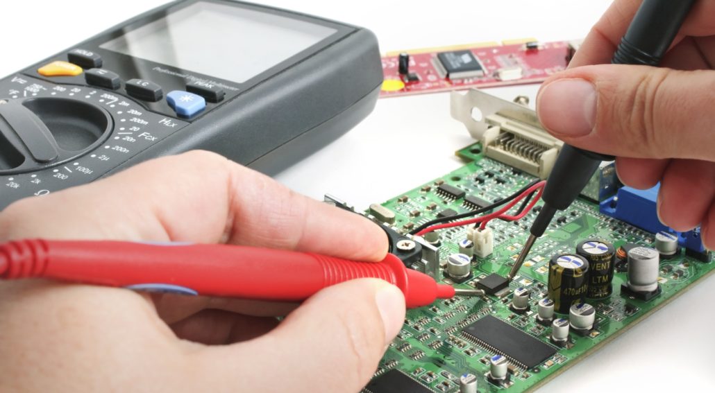
Once the first prototype comes back it will now need to be evaluated and if any problems are found, those will need to be debugged.
Examples of blank (before components are soldered on) Printed Circuit Boards (PCBs).
Debugging a new circuit is a difficult step to forecast, because until you know what the problem is, you can’t estimate how long it will take to fix it.
Step #4 – Program the Microcontroller
Almost all electronics products today have some kind of microcontroller that acts as the brains for the product.These are almost always programmed in a computer language called “C”. If the program needs to be super efficient or fast then parts of it may be done in assembly language.
Sometimes the programming will be done by the same person that designed the circuit, but many times a software specialist is brought in to do the programming.
Step #5 – 3D Modeling
This is almost always handled by a different engineer than who did steps 1 thru 4.In the beginning all you really need is a 3D modeling expert, especially if you have a good vision of what your product should look like.
Eventually you may want to hire an industrial design engineer to really make it look good. For example, industrial designers are the engineers responsible for making Apple’s products look so cool.
Either way make sure whoever does the 3D model design has experience with injection molding technology. 3D printing is used for low-volume prototyping, but injection molding is used for high-volume manufacturing. It’s a common mistake for 3D designers to create a model that can be 3D printed but not injection molded.
XXX . V000 How Much Does a Prototype Cost?
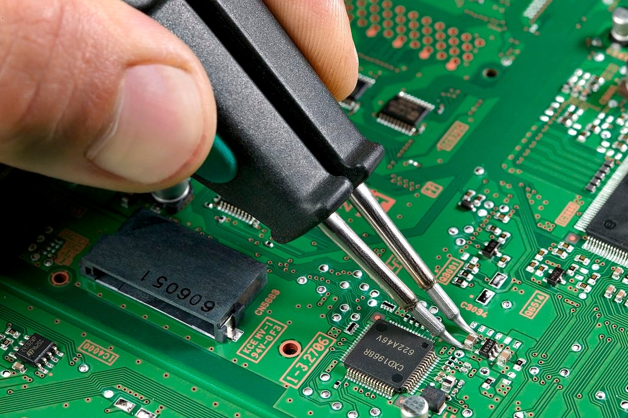
The total cost of the prototype (assuming an electronic product) usually includes the cost to manufacture the custom Printed Circuit Board (PCB), plus the cost of assembly, plus the cost of the components, plus the cost of the enclosure prototype.
Engineering costs vary greatly depending on the product complexity, engineering specialty required, product size desired (smaller usually takes longer and thus costs more), location, etc.
For more details on all the costs be sure to read my really in-depth article on the costs to develop, scale, and manufacture a new electronic product.
Most engineers work on an hourly basis especially on larger projects. Be warned though that it’s impossible to quote the development time for a complex product exactly down to the hour. So you should expect your costs to exceed what is initially estimated.
The hourly rate charged by design engineers varies depending on years of experience, education level, area of specialty, success with previous projects, etc. According to the Institute of Electrical and Electronic Engineers (IEEE) the national average rate for an independent contract engineer is $125/hr.
For example, a more expensive engineer may be able to work twice as fast and produce a higher quality of work, both of which will lower your overall cost.
Although it may be tempting to use cheaper offshore engineers that is usually a mistake. With lots of experience you can safely outsource small, well-defined tasks to offshore engineers, but never the entire development. And never unless you actually have the skills necessary to do the job yourself, otherwise you have no way to confirm the quality.
PCB Production Costs
The cost to produce a few blank PCB boards usually runs about $750. This assumes their most basic manufacturing process, and if you want a super small board then more advanced, more costly processes have to be used.To produce a prototype PCB I use a company called Sunstone Circuits.
If you are familiar with the basics of PCB design then you can use Sunstone’s PCB Instant Quote tool to estimate the cost.
Most boards require 4 layers. Adding more layers can help reduce the board size but at a higher cost. Although the cost decreases as the board size decreases, the number of layers has a much greater impact on cost. So bigger boards with few layers are cheaper than smaller boards with more layers.
Advanced PCB technologies, like blind and buried vias, can also be used to decrease board size even further. But these technologies will add thousands to your prototyping costs so only use them if absolutely necessary.
Wearable tech, for example, is extremely size sensitive and must be as small as absolutely possible. So with wearable tech I normally start with a larger than desired board size for the first prototype version.
Starting with a larger board accomplishes three things. First, it lowers the production cost of the boards. Second, it lowers engineering costs to develop the boards, because a bigger board is quicker to design and easier to debug. This means less engineering hours.
After the basic functionality has been confirmed then you can squeeze the board size down, if you really need it super duper small.
PCB Assembly Costs
For a couple of boards with say 30-50 different components the cost is approximately another $750 – $1,000.For assembly (which means soldering all of the electronic components onto PCB)
Cost of the Electronic Components
In addition to the board production and assembly costs, there is the cost for the electronic components.But for most products the cost of the components is minimal and usually totals less than about hundred dollars for a few boards.
Enclosure Prototyping Costs
As for the enclosure (a.k.a. the case) the cost depends if you want a custom design or if you can get by with a stock enclosure.A stock enclosure will usually only cost a few dollars. A custom enclosure will cost several hundred dollars depending on the size, complexity and number of pieces needed.
For prototyping any custom plastic or metal parts I highly recommend Proto Labs. They offer various prototyping services as well as creating low volume injection molds that allow you to produce a few thousand parts.
Try to get by with a stock enclosure as long as possible to save money and complication. However, most products eventually require a custom designed case so you can’t delay that complication indefinitely.
Summary
Keep in mind that all of these costs will reduce significantly as your production volume increases. Even going from 2 units to 20 units has a huge impact on the unit price.What costs you a thousand dollars for a single prototype may only cost a couple of dollars once you purchase much higher volumes.
XXX . V0000 Why You Should “Pre-Design” Your Product
Define your product, design it, then manufacture it. Right? Well, not exactly. Although, this is the process most entrepreneurs follow, it’s not the process you should follow.
Before you jump head first into fully designing your product you really need to look at the big picture. This will allow you to answer many questions earlier than otherwise. The best way to achieve this early insight is by inserting an intermediate step between defining your product and designing it. This intermediate step is a pre-design, or preliminary design.
By pre-design I mean to design the product with just enough detail to answer some important questions. But without worrying yet about the tiny details that don’t have a big impact.
The problem is that once you dig into the full design you tend to get buried in the technical details. The old saying you can’t see the forest through the trees definitely rings true in this situation. To be a successful founder you need to see both the trees and the forest! For example, with electronics design most of the cost and functional impact is related to the microchips (integrated circuits – ICs). The secondary components, such as resistors and capacitors, don’t really matter that much. Their cost is usually negligible once you reach manufacturing volumes.
The exact specifics of how all of the various electronic components connect together also doesn’t really matter at this early stage. Sure, you need to define in broad terms how the components will interface, but you don’t need to worry about the small details yet.
For example, if a sensor connects to a microcontroller you should define the interface as being I2C (a 2-wire serial protocol common with sensors). But, at the pre-design stage you don’t need to worry about details like the pin numbers or the value of the required pull-up resistors.
When designing a new product most of the work is in the details. But in most cases those details don’t really have much of an impact on the big picture.
For a typical product here are the steps I perform as part of the pre-design stage:
1) Identify each core function such as the microcontroller, Bluetooth, sensors, power management, etc.
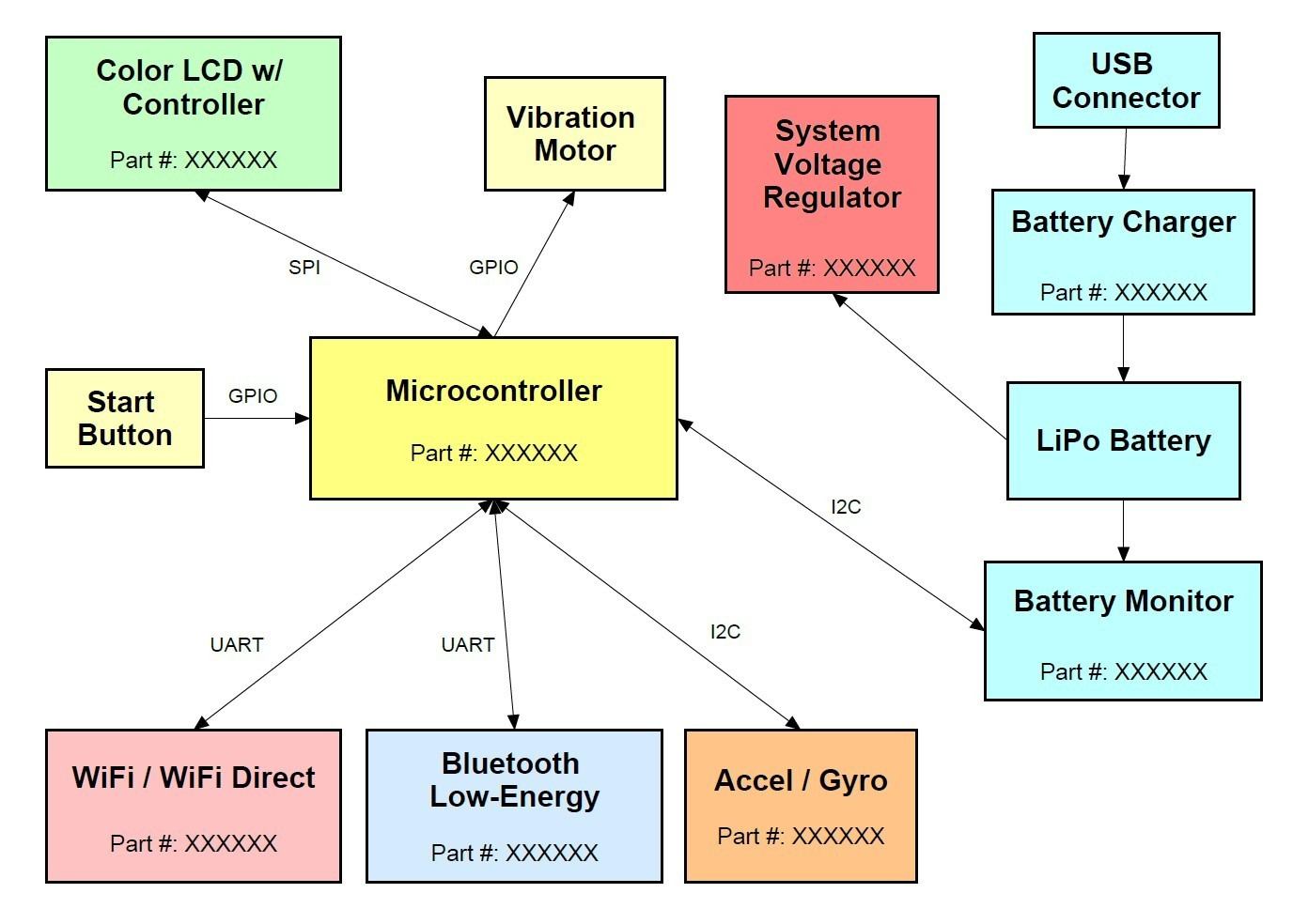
2) Create a block diagram showing how to incorporate all of these core functions.

Figure 1 – Example of a block diagram
3) Define how the components will be interconnected by specifying UART, I2C, SPI, I2S, GPIO, AIO, USB, MIPI, etc. Don’t worry if you have no idea what these acronyms mean. Just know that specifying them in the block diagram is critical to selecting the right electronic components, especially the microcontroller or microprocessor (the “brains” for your product).
4) Select the best microchips to perform the various product functions. This is the most important step of the pre-design stage. Lots of things need to be taken into account when selecting the critical components such as performance, cost, availability, manufacturer support, packaging, physical size, and the forecasted End-of-Life (EOL).

Figure 2 – Various examples of electronic microchips (integrated circuits).
5) Estimate the size of the Printed Circuit Board (PCB) required and the number of layers needed. This helps to determine the minimum required size for your product, as well as the manufacturing cost of the PCB.
6) Estimate the number of BOM components, number of PCB pads, whether components will be soldered on both sides of the PCB, etc. These are all details that will allow you to eventually estimate the cost to manufacture your product (more on that in a bit).
7) Determine the number, size, and general shape of any custom shaped plastic pieces required for the enclosure. This information allows you to estimate the cost for the injection molds that will be required to scale from prototype to mass manufacturing. It will also allow you to estimate the manufacturing cost for your enclosure.
8) Ascertain the complexity of final assembly for the product. Are there lots of pieces that all have to squeeze into a tiny enclosure very carefully? If so, this will impact the cost to assemble the product. Ideally, you can estimate how long it should take to assemble your product.
9) Finally, give some thought to how complex it will be to test your product during manufacturing? Ideally try to estimate how long it will take to properly test it. How long this takes will impact the manufacturing cost.
Can your product even be realistically developed? How much will it cost to develop and scale? How much profit can you make? What distribution strategy should you pursue? How much should you sell the product? These are just some of the questions that a pre-design can help you answer before you actually begin fully designing the product.
Pre-designing your product before you start on the full design has many advantages. Let’s now discuss some of these advantages.
See the big picture
As I said, most entrepreneurs focus solely on the product they are developing. But remember, you’re not developing a new product, you’re developing a new company!Repeat after me, “I’m creating a company, not just a product”. Any time you find yourself absorbed in the details of development remind yourself of this fact.
Unless you’re one of the rare few who can license out their product, you won’t ever get rich creating a new product. If you want to truly get rich you have to focus your efforts on creating a successful company, not just a successful product.
The more technical you are the more likely you are to over focus on the development details too early. This is because technical entrepreneurs tend to put 100% of their focus on product development. Development is what they are most comfortable doing. They have the mindset that they’ll worry about all the other stuff (costs, marketing, sales, etc.) once they get through product development. If you are focusing solely on development then you’re acting as an engineer, not a founder/entrepreneur. As a founder you have to wear lots of hats, not just those in your comfort zone. Pre-designing your product helps you to better see all the other aspects of launching a new product (and company).
Identify key development challenges
The earlier you identify your key development challenges the better. The worst case strategy that I’ve seen is to focus first on developing the easy parts of the product. In fact, you should do just the opposite. Focus first on solving the most challenging parts of your product.Performing a pre-design before you get lost in the fine details of product design allows you to more easily identify the parts of your product that will be the most challenging.
Once you do identify the critical challenges you should come up with the solution before you proceed beyond the pre-design stage. Pre-design is really all about identifying the best solutions without worrying about the non-critical details.
Pre-design is a top-down approach to product design. You start at a high-level and then work your way down to lower levels as needed. This is in contrast to a bottom-up design strategy where you start by fully designing each sub-function, and then eventually connect them all together into a whole system.
Entrepreneurs tend to follow the bottom-up approach, whereas established companies developing new products usually will implement a top-down approach.
The top-down approach allows for more structured control of a project which usually leads to minimized costs. This is why most companies that regularly develop new products typically follow a top-down approach.
You will save money and be more successful if you follow the top-down approach. To succeed with product development you need a structured process.
Accurately estimate of all costs
An important benefit of pre-designing your product is that it allows you to accurately estimate all of the costs to launch your product. This includes the cost to fully develop and prototype it, the cost to scale it from prototype to mass manufacturing, and most importantly the actual cost per unit to manufacture it.Although it’s possible to estimate the development cost for a new product without a pre-design, your estimate will be much more accurate if you have a pre-design. The same is true with scaling costs.
However, in order to estimate the manufacturing cost a pre-design is absolutely necessary. In fact, this is one of the most important reasons to pre-design a product.
Most entrepreneurs, makers, and even engineers spend months or years designing their product. Once they finally have a perfect prototype then they’ll calculate the manufacturing cost. But by then you have little flexibility to control the manufacturing cost, unless you go back and do a redesign.
Knowing the cost to manufacture your product, also called the Cost of Goods Sold (COGS) is probably the most important number you should know. After all, the manufacturing cost determines both your sales price and your profit.
Remember you’re developing a company, not a product. And nothing is more important for a company than profit!
Select the best feature set
Having a pre-design, and accurate manufacturing cost estimates, allows you to individually price out each feature of your product. By knowing the additional manufacturing cost for each feature you can then select the most economically optimal set of features for your product.For example, perhaps you are debating if you should incorporate GPS tracking in your product. Your market research shows that GPS can increase your sales price by $20.
But once you price out this feature you realize it will add $15 to your manufacturing cost. Based on this data you may then decide it doesn’t make sense to add GPS because the profit margin is too low for that feature.
Determine best distribution strategy
Determining the best distribution strategy for your product depends on many variables but it especially depends on the manufacturing cost, or more accurately the profit margin. As your manufacturing volume increases your manufacturing cost will decrease and your profit margin will increase.Because of this fact, your distribution strategy may vary depending on your manufacturing volume. For example, when manufacturing volumes are low your manufacturing cost will be high.
Selling your product directly to consumers is likely your best distribution strategy in this scenario. Selling direct to consumers will maximize your profit margin. The most popular way to do this is to sell your product on your website, or perhaps through Amazon.
Later, as your manufacturing volumes increase and your manufacturing cost decreases, you will have the profit margins necessary for selling via retail outlets. Selling through retail outlets means there are more people taking a piece of the pie. This necessitates lowering the manufacturing cost in order to make this distribution strategy profitable.
Plan a better strategy to market
Until you understand the key developmental challenges, as well as the costs to develop, scale, and manufacture your product it will be impossible to plan the best strategy.For example, without knowing your development and scaling costs you’ll have no idea how much capital will be needed to get your product to market. Without this information you’re likely to run out of money before your product reaches the market.
Early feedback from developers and customers
Incorporating a pre-design stage into your development process gives you an opportunity to get early feedback from developers, manufacturers, and even potential customers.To get this feedback it’s best if you have more than just an idea. You should show some upfront work to support your product idea. Sure, a pre-design is still just an idea, but it’s an idea with some serious development behind it. Because of this a pre-design can be useful for gathering feedback.
Reduce your manufacturing cost
By putting more focus on costs early in the development process, you’ll have more opportunities to lower these costs. A pre-design allows more thought toward selecting the best priced components.This is in contrast to the typical process of designing the product then later calculating the manufacturing cost. Following that process will give you very little flexibility to control your product’s manufacturing cost.
Minimize your scaling costs
Pre-design allows you to make better decisions that can help reduce the costs to scale your product from prototyping to mass manufacturing.For example, one important element of a pre-design is to determine how many custom shaped pieces of plastic will be required for the enclosure. Minimizing the number of plastic pieces you can have a drastic impact on reducing your scaling costs.
This is because each custom piece of plastic requires its own expensive injection mold. These mold costs are one of the most expensive obstacles you’ll face taking your product to market.
Creates early opportunity to raise outside funding
You definitely need more than just an idea to get others interested in investing in your product. The idea is the easy part. Almost everyone has new product ideas but very, very few have the determination to bring it to market.The first piece of information you need in order to raise money is how much money you need. If you don’t raise enough you’ll run out before you make it to market. Trying to raise more than really needed will present an unnecessarily difficult challenge.
Having a pre-design and solid estimates on all of the costs required is essential to raising early capital. Investors want to see some solid research and development to back up your product. A production-quality prototype is ideal, but many entrepreneurs have to raise outside capital before they can afford to produce a high-quality prototype.
Final thoughts
As an entrepreneur myself I completely understand how excited you are to bring your product idea to reality. This excitement is necessary for you to be able to surpass all of the obstacles in your path to market.But, this excitement can also lead you to rush getting your product on the market. Time to market can be critical but you also need to take the necessary steps to ensure that you are proceeding down the right path.
You don’t want to ever be in the position of discovering that you’ve hurried up and developed the wrong product, or developed a product that you can’t manufacture and sell at a profit.
One of the best ways to prevent this scenario is to first create a high-level pre-design of your product. Starting with a pre-design will give you enough information to see the forest before you get lost in the trees.
XXX . V00000 How long does it take to develop a new product and get it to market?
Last week I answered the most common question I am asked. This week I answer the second most common question. Obviously everyone wants to know how long this whole process is going to take to bring a new hardware product to market.
The simple answer is: a long time. The more accurate answer depends on many variables, including: Variable #1 = You
Yes, you are the biggest determining factor to how long it will take to develop and manufacture your product. The truth is no one will ever work as hard or as fast as you (and any co-founders).
If you have all the necessary technical skills to develop your own product, then doing it yourself is the fastest way to market. But that’s rare, and even if you’re an engineer you will likely have to learn many new skills.
For example, the hardware product that I brought to market back in 2010 required significant mechanical designing and 3D modeling. Since I’m an electronics engineer I hired a mechanical engineer to help develop my product. Being an excited entrepreneur I wanted things to move fast. I was very impatient and I’m sure the engineer I hired thought I was a pain to work with. He didn’t work fast enough to suit me so I switched to another mechanical engineer. But the second engineer wasn’t fast enough for me either.
Finally, I decided to teach myself 3D modeling and how to design for injection molding so I could finish the mechanical design myself. This helped to drastically speed up the development of my product.
The positive impact of doing a design yourself is more significant when appearance is critical since getting the “look” of a product right requires a lot of back and forth communication.
There are two morals to this story: First, no one can ever out work an excited, hyper-focused entrepreneur with a vision! Second, knowledge is power so the more you learn the more likely you are to succeed, quickly.
Variable #2 = The Product
Another critical variable that determines the time to market is the product itself. The more complex the product the longer it will take to develop and scale to manufacturing.For example, it’s going to take you much longer to develop a complex robot with vision and speech recognition capabilities, than it will to develop a relatively simple Bluetooth Low-Energy product.
You can break down the product development into discrete steps, some easier than others to accurately estimate.
For example, with the necessary experience it’s relatively easy to estimate how long it will take to design the electronics schematic, or the Printed Circuit Board (PCB).
However, estimating the time needed to debug any issues found in your prototype is much more challenging. The first prototype for any new product is never perfect, and there will be problems that need to be fixed.
By its very nature, finding and fixing a bug means you are dealing with unknowns. If it was known you likely wouldn’t have designed it to have this bug, right? This is why debugging can be a challenging step to properly forecast.
One way to reduce your time to market is to focus initially on getting a Minimum Viable Product (MVP) version to market.
To be brutally honest, you don’t have a proven product idea until its actually on the market and you see what consumers really want . You may think your idea is a winner, but you cannot be sure.
The only way to know what consumers truly want is to sell them your product and get their feedback. Then you can implement this feedback to create the product they really want to buy.
So you need to focus on getting the simplest version of your product to market as fast as absolutely possible. Then use the feedback from users to fine-tune the product to include the features that buyers really want.
#3 – Money
Although you and your product are the most critical factors impacting the time to market, of course money is important.That being said, the careless use of money may actually increase the time to market. This is especially true for first time product entrepreneurs. Don’t make the mistake of throwing lots of money at a problem you don’t fully understand.
It’s unrealistic to think you can do everything yourself, but the more you do yourself the better off you will be.
Okay, everything I’ve said so far is rather abstract. You want some concrete numbers on how long it will take to get your product to market, right?
If you have an experienced product developer on your founder team, and you have a product of moderate complexity, then you should be able to get your first prototype within about 3 months, and a final works-like-looks-like prototype within about 6-9 months.
If you have little product development experience on your team, then it will likely take longer. In this scenario the amount of money you have to spend is an important factor since you will need to outsource product development.
In order to pay to outsource your product’s development you may need to take it a bit slower to give you enough time to spread out the costs. If you run out of money then you may be forced to put a hold on development while you save more money. But that’s okay, and you should never spend more than you can afford to lose.
A final works-like-looks-like prototype doesn’t necessarily mean it’s ready to be manufactured. Typically, additional time will be required to fully optimize the design for manufacturing.
For example, although you may have a plastic enclosure that can be prototyped, you’ll now need to prepare that enclosure design for injection molding.
I would suggest you allocate an additional 6-9 months after having a final prototype to get your product ready for mass manufacturing. During this time you should also take care of additional steps such as obtaining the necessary electrical certifications.
To summarize, if you can get your product from concept to market in the fastest way possible, it will take about one year. That time frame applies to the ideal situation, meaning you have lots of development and manufacturing experience on your team, you have a good amount of capital to spend, and your product is moderately simple.
But to be honest this is a very rare situation. You really need the stars to align in order to take a concept to market in only one year.
For most founders and products, two years is more realistic. Taking one year for development plus one year to scale to manufacturing is an achievable goal for most hardware startups.
This is why you really need to have a long-term mindset. Bringing a new hardware product to market is always slow, even for experienced tech companies. Although time to market can be critical, don’t rush. Most likely you will be working on bringing your product to market for years.
XXX . V0000000 How can I get my product to market if I have no money or experience?
You must remember that the true value is in the execution of an idea, and not just the idea alone. This is why no one steals product ideas, instead they wait and “steal” successful, proven products.
This means that to succeed with your product you’re going to have to commit to doing more than just coming up with the great idea. The idea is the easy part, but nothing of real value is ever easy. There are really two assets you can bring to the table beyond just the idea: money or knowledge. But you don’t have either, right? So what should you do?
First of all, without much money and little to no experience, you’re going to have to accept that this process is going to take you longer. But, that’s okay. This will be a long journey regardless of what assets you bring to the project.
Secondly, you’re going to need to focus on raising some level of capital. It’s literally impossible to get a new product on the market without any money. The good news is you don’t need to finance everything yourself, but you will need to invest at least enough money to get the product to the point that you can entice others to invest their money and time.
Third, you need to focus considerable effort on learning some new skills to bring to the project. The less money you are able to invest, the more skills you’re going to have to learn.
There are two broad skill categories you need to focus on: technical and marketing.
Unless you have a co-founder, you’re going to need to learn both of these skills. If you like technical stuff then bring on a co-founder that excels at marketing. Vice versa, if marketing is your strength, then bring on a technical co-founder.
Unfortunately, finding a compatible co-founder can be almost as difficult as finding investors, so you likely will need to learn both technical and marketing skills yourself.
If you’re a maker, then good for you, that’s a great start. If you’re not a maker, then you probably need to become one.
Buy yourself an Arduino or Raspberry Pi, and focus on learning some basic electronics.
If your product requires a microcontroller then get an Arduino. If it requires a microprocessor and an operating system then get a Raspberry Pi. If you are unsure which is needed then read this article.
In addition to the Predictable Designs blog, spend time learning from websites such as Adafruit, Sparkfun, Build-Electronic-Circuits, and BaldEngineer.
As far as money is concerned you need to save up enough to at least get the product far enough along that you can get others to invest. For most products, this is going to require at least a few thousand dollars.
Ideally, you can get the product to a point of having a production quality prototype, but that will take at least about $10,000.
If that’s more than you can ever hope to afford, then try to at least put together a Proof-of-Concept (POC) based on a development kit such as the Arduino or Raspberry Pi. For more about the various types of prototypes see this article.
If creating a POC prototype is still too complicated or expensive for you to do on your own, then your best option is to get a realistic animation video created that demonstrates your product.
A digital model of your product is your best shot at getting outside investments if you can’t afford to create a real prototype.
I personally advise against getting investments from friends and family. This may just create friction for you down the road, especially if your product ends up failing.
Although more difficult, you are much better off getting “strangers” to invest in your product. By getting strangers to invest not only do you raise precious capital but you also gain a bit of social proof that your idea is a good one.
The best way, although definitely not the easiest, is to raise money via a crowdfunding campaign. Crowdfunding can provide you both money and lots of social proof.
The only way to ever really know if a product will sell is to try to sell it. Normally, that requires you have the finished product ready to sell. But crowdfunding allows you to essentially sell your product to potential investors without a real product to sell yet.
To do that you’re going to need at least three elements: an audience, a physical prototype or at least a digital model, and accurate estimates on how much it will cost to develop, scale, and manufacture your product.
So to quickly summarize, focus on saving money, learning new skills, making connections, and building an audience. Finally, constantly remind yourself that the value is in the execution, and that it’s the journey that counts not the destination.
Most importantly, try to have fun! Because this will be a long journey, and there are no overnight successes in any type of business.
XXX . V0000000 Online & Offline Circuit Design Software for Beginners and Professionals
The technological advancement and easy access to the internet have made everything convenient for the masses, be it a routine activity or a professional task. Previously, we covered the list of circuit design tools, and online circuit simulators for electronics designers that render great ease in the completion of electronic projects. Likewise, there are various online software that can assist the engineers while dealing with the circuits.
Circuits are the most basic and integral part of every electronic device and hence anyone belonging to the electronics field has to get acquainted with their designing and development. In such a situation, these software allow everyone to learn and design circuits for both educational and professional purposes.
Here is a compilation of some online & offline circuit design software that are quite popular among the designers and hobbyists.
1. Zenit PCB (FREE DOWNLOAD)
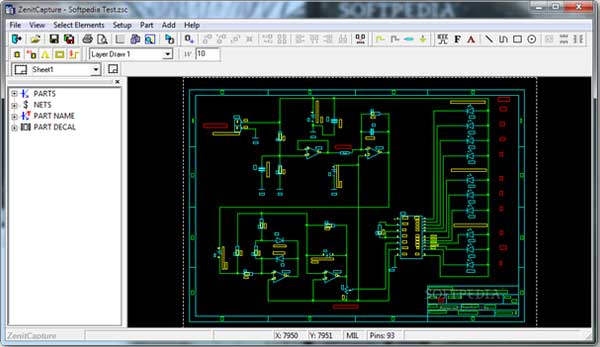
Zenit PCB is excellent software for designing electronic circuits with the use of various components. It is meant to be used for semi-professional projects as it imposes the restriction of using up to 800 pins. There is a black colored board with a grid on which components can be added with a right click. Another click on the parts option will provide access to a library of the parts. Besides, a click on the placed components will reveal their properties on the left side panel.
The project can be saved in .ZSC format and one can also take out a copy in the form of a printout. Moreover, the project report can be exported in TXT format including the project name, author, number of parts, pins, etc. There is also a user guide in PDF format in the help menu.
2. KiCad EDA (FREE DOWNLOAD)

KiCad is a free software suite meant for electronic design automation (EDA). It’s a cross-platform circuit design software that is compatible with all the operating systems like Windows, Linux, and Mac OS X. It is available with three tools namely schematic editor, PCB layout, and 3D Viewer which let you design the circuit by adding and editing components, decide the layout of the PCB and then have a 3D view of the prepared circuit.
The components offered in the software include Microchip, Display, Audio device, Memory, Power, Transistor, etc. additional components like wire, ground, junction, and bus can also be chosen. Besides, there is a PCB Footprint Editor for adding footprint to the PCB and two more tools namely Bitmap2Component converter and a PCB Calculator.
3. Fritzing (FREE DOWNLOAD)
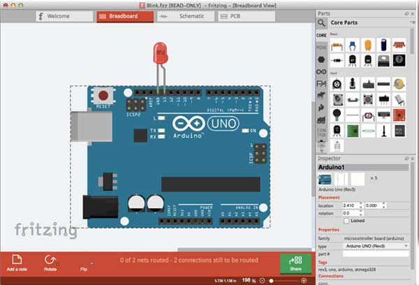
Fritzing is an open source circuit design software which is meant for the Windows users. It is an initiative that aims at making the electronics accessible for everyone and can be used for Arduino prototyping as well as for designing PCBs. It is an ideal tool not merely for the hobbyists but for the non-engineers for learning, designing and sharing the knowledge of circuits.
The components available with Fritzing are resistors, ICs, switches, gates, diodes, junctions, wires and so on. The file can be saved in .FZZ format and the users can even add a note or rotate the PCB board. It also enables the user to export the designs as PDF or image. Also, there are different modes to view the design namely breadboard, schematic, PCB and code. Lastly, there is a Help page to provide assistance in case the user faces any difficulty in the designing.
4. Easy EDA (online)
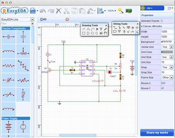
EasyEDA is a free web and cloud-based EDA tool suite which doesn’t need any installation. It is an integration of a powerful schematic capture with a mixed-mode circuit simulation and PCB layout in a cross-platform environment. It can be used by a wide array of users including students, educators, hobbyists, and engineers.
This software allows users to create and edit schematic diagrams and PCB layouts, simulation of analog and digital circuits along with the option of manufacturing PCBs. Some other features offered by the software are- creation of Bill of Materials, Gerber and pick or place files as well as documentary outputs in PDF, PNG and SVG formats.
5. TinyCAD (FREE DOWNLOAD)
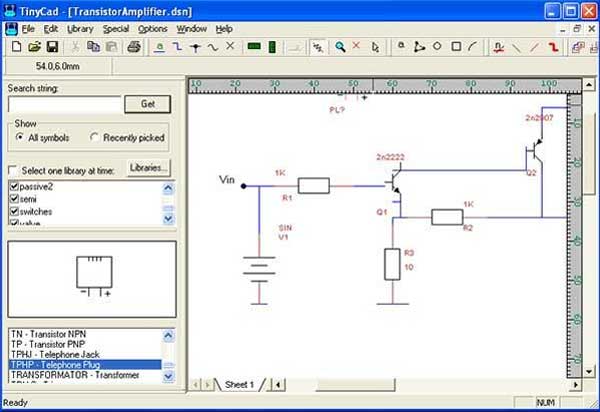
TinyCAD is yet another open source and free of cost program for the Windows users. It is offered with complete sign symbol libraries alongside tools like schematic capture and PCB layouts. The circuits can be designed with the help of following components like logic gates, relays, capacitor, diodes, switches, power sources, and microcontrollers. Further, there are wires, text, symbols, and shapes for finalizing the connections of the circuit.
The users can also print their designs and publish them through the copy paste function in the form of a document, or save them as PNG bitmap image or the web. After getting done with the design, the file is saved in .dsn format.
6. Proteus (PAID)
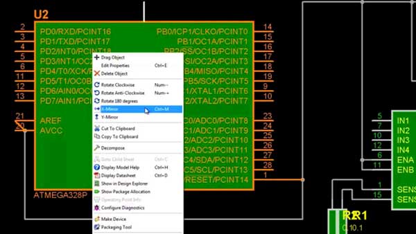
Proteus is a paid tool for EDA available for different platforms including Windows, MAC, and Linux. It allows the users to create and deliver PCB designs with a highly professional appeal. It’s claimed to be a complete software package meant for the engineers. The software carries a built-in STEP export and a global shape based auto router as a standard facility. Moreover, there are more than 785 microcontroller variants for the simulation.
It has got modules like schematic capture, microcontroller simulation, PCB design and 3D verification. Since its paid software, the users can buy it many configurations, depending on the size of designs and the need for microcontroller simulation.
Pricing
The standard feature set is available for purchase at $487 whereas the Professional Feature set is offered at $1,642.
7. PCB Artist (FREE DOWNLOAD)
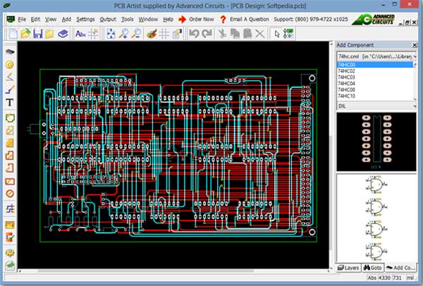
This is free of cost PCB design software that offers top PCB layout capabilities along with Live Technical Support. The users can also avail features like “Multi-Page schematic and “Netlist Import.” Another advantageous feature is that it contains a components library with more than 500,000 parts. Some of these components are EEPROM, Relays, LEDs, diodes, switches, capacitors, and other ICs. The designed files are saved in .pcb format and there is even an option named order now for ordering the designed PCBs
8. Circuit Maker (FREE DOWNLOAD AFTER SIGN UP)
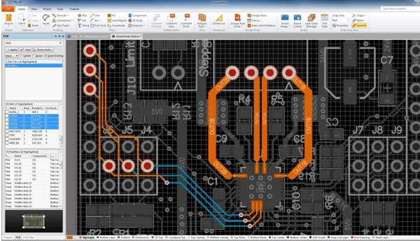
Circuit Maker is desktop-based online software that helps in designing circuits on Windows. The users have to first sign up on the website and then they can launch the application. This software needs an internet connection to work and hence the designed circuit is saved online rather than on your device.
An interesting feature of this tool is that it carries a collaboration facility which lets you work in teams. The user can add members and then they can work in collaboration on the electrical design project. After the completion you can either release the design to be viewed by anyone or you can submit it so as to be shared with the team members.
9. Free PCB (FREE DOWNLOAD)
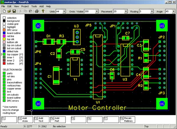
It’s open source PCB design software that is meant to be used in the Windows system and supports up to 16 copper layers and board sizes of up to 60X60 inches. The users can also apply footprints and utilize the feature of Design Rule Checker.
The list of components available with this software includes the likes of resistors, capacitors, connections, transistors, ICs, LEDs, and connectors. The Project menu holds Parts option which reveals all the parts in the circuit with information and then the Nets option are used to view all the connections.
10. Eagle (PAID)
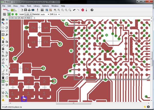
Eagle stands for Easy Applicable Graphical Layout Editor and its free version can be availed to design circuits for non-commercial purposes. It’s compatible with all operating systems like Windows, Mac, and Linux and offers 3 modules which are- Schematic Editor, Layout Editor, and Autorouter.
The users can build circuits using components like optos, filters, comparators, diode, symbols, supply, opams, etc. Further, clicking on each component reveals the attributes like name, symbol, property, etc. Besides, the user can right-click on a device and apply functions like rotate, delete, and copy. The Eagle circuit drawing and bitmap files can be imported while the net-list, pin-list and part-list can be exported.
Pricing
It has 5 versions named Standard ($69), Premium ($820), Ultimate ($1640), and Premium LS ($575), and Ultimate LS ($1145).
11. ProfiCAD (FREE DOWNLOAD)
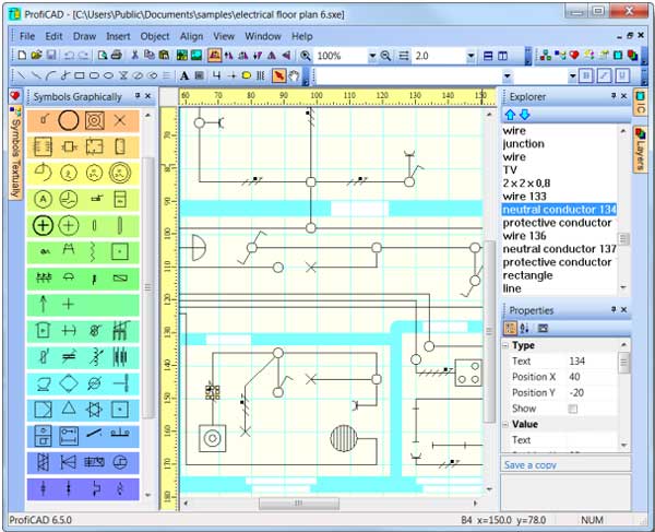
This software has been designed to draw electronic diagrams, schematics, control circuit diagrams and can also be used to draw other kinds of technical diagrams. The components found in this software are namely LCD, measurement devices, circuit breakers, diodes, resistors, indicators, rheostats, house electrical devices and so on.
The grids available on the workspace enable the user to create hassle-free diagrams which can be saved in .sxe format. One can also preview and print the design directly from this software. It integrates modern programming and advanced optimization which in turn demands less disk space and also fits in your budget.
12. Logisim (FREE DOWNLOAD)
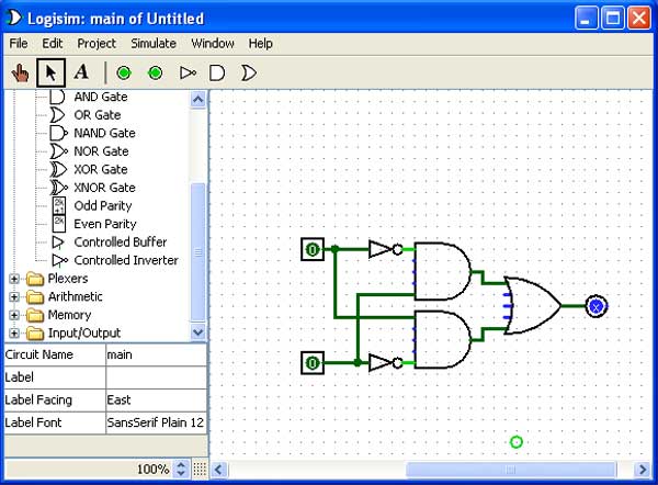
Logisim is a free of cost as well as open source tool for designing and simulating digital logic circuits. It is very helpful in learning about the basic concepts of logic circuits as it offers an easy to use toolbar interface. One can find the following list of components in this software:
• Logic Gates
• Input/output Circuits
• Multiplexer
• Arithmetic Circuits
• Flip-flops
• Multiplexers
• Power
• Ground
The completed designs are saved in .circ file which can be further exported to a GIF file or can be printed on a printer. There is a combinational analysis module that enables the users to take on conversion between circuits, truth tables, and Boolean expressions.
XXX . V00000000 Physical design (electronics)
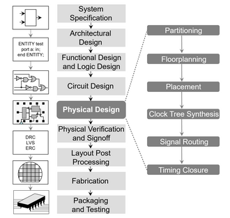
In integrated circuit design, physical design is a step in the standard design cycle which follows after the circuit design. At this step, circuit representations of the components (devices and interconnects) of the design are converted into geometric representations of shapes which, when manufactured in the corresponding layers of materials, will ensure the required functioning of the components. This geometric representation is called integrated circuit layout. This step is usually split into several sub-steps, which include both design and verification and validation of the layout.
Modern day Integrated Circuit (IC) design is split up into Front-end design using HDLs, Verification, and Back-end Design or Physical Design. The next step after Physical Design is the Manufacturing process or Fabrication Process that is done in the Wafer Fabrication Houses. Fab-houses fabricate designs onto silicon dies which are then packaged into ICs.
Each of the phases mentioned above has Design Flows associated with them. These Design Flows lay down the process and guide-lines/framework for that phase. Physical Design flow uses the technology libraries that are provided by the fabrication houses. These technology files provide information regarding the type of silicon wafer used, the standard-cells used, the layout rules (like DRC in VLSI), etc.
Divisions
Typically, the IC physical design is categorized into Full custom & Semi-Custom Design.- Full-Custom: Designer has full flexibility on the layout design, no predefined cells are used.
- Semi-Custom: Pre-designed library cells (preferably tested with DFM) are used, designer has flexibility in placement of the cells & routing.
ASIC Physical Design Flow

A typical ASIC back-end flow
- Design Netlist (after synthesis)
- Floorplanning
- Partitioning
- Placement
- Clock-tree Synthesis (CTS)
- Routing
- Physical Verification
- GDS II Generation
- Cadence (Cadence Encounter RTL Compiler, Encounter Digital Implementation, Cadence Voltus IC Power Integrity Solution, Cadence Tempus Timing Signoff Solution)
- Synopsys (Design Compiler, IC Compiler)
- Magma (BlastFusion, etc.)
- Mentor Graphics (Olympus SoC, IC-Station, Calibre)
The ASIC physical design flow uses the technology libraries that are provided by the fabrication houses. Technologies are commonly classified according to minimal feature size. Standard sizes, in the order of miniaturization, are 2μm, 1μm , 0.5μm , 0.35μm, 0.25μm, 180nm, 130nm, 90nm, 65nm, 45nm, 28nm, 22nm, 18nm, 14nm, etc. They may be also classified according to major manufacturing approaches: n-Well process, twin-well process, SOI process, etc.
Design Netlist
Physical design is based on a netlist which is the end result of the Synthesis process. Synthesis converts the RTL design usually coded in VHDL or Verilog HDL to gate-level descriptions which the next set of tools can read/understand. This netlist contains information on the cells used, their interconnections, area used, and other details. Typical synthesis tools are:- Cadence RTL Compiler/Build Gates/Physically Knowledgeable Synthesis (PKS)
- Synopsys Design Compiler
Physical Design Steps
Floorplanning
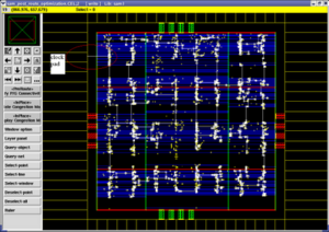
The first step in the physical design flow is Floorplanning. Floorplanning is the process of identifying structures that should be placed close together, and allocating space for them in such a manner as to meet the sometimes conflicting goals of available space (cost of the chip), required performance, and the desire to have everything close to everything else.Based on the area of the design and the hierarchy, a suitable floorplan is decided upon. Floorplanning takes into account the macros used in the design, memory, other IP cores and their placement needs, the routing possibilities, and also the area of the entire design. Floorplanning also determines the IO structure and aspect ratio of the design. A bad floorplan will lead to wastage of die area and routing congestion.
In many design methodologies, Area and Speed are the subjects of trade-offs. This is due to limited routing resources, as the more resources used, the slower the operation. Optimizing for minimum area allows the design both to use fewer resources, and for greater proximity of the sections of the design. This leads to shorter interconnect distances, fewer routing resources used, faster end-to-end signal paths, and even faster and more consistent place and route times. Done correctly, there are no negatives to floorplanning.
As a general rule, data-path sections benefit most from floorplanning, whereas random logic, state machines, and other non-structured logic can safely be left to the placer section of the place and route software.
Data paths are typically the areas of your design where multiple bits are processed in parallel with each bit being modified the same way with maybe some influence from adjacent bits. Example structures that make up data paths are Adders, Subtractors, Counters, Registers, and Muxes.
Partitioning
Partitioning is a process of dividing the chip into small blocks. This is done mainly to separate different functional blocks and also to make placement and routing easier. Partitioning can be done in the RTL design phase when the design engineer partitions the entire design into sub-blocks and then proceeds to design each module. These modules are linked together in the main module called the TOP LEVEL module. This kind of partitioning is commonly referred to as Logical Partitioning.Placement
Before the start of placement optimization all Wire Load Models (WLM) are removed. Placement uses RC values from Virtual Route (VR) to calculate timing. VR is the shortest Manhattan distance between two pins. VR RCs are more accurate than WLM RCs.Placement is performed in four optimization phases:
- Pre-placement optimization
- In placement optimization
- Post Placement Optimization (PPO) before clock tree synthesis (CTS)
- PPO after CTS.
- Pre-placement Optimization optimizes the netlist before placement, HFNs are collapsed. It can also downsize the cells.
- In-placement optimization re-optimizes the logic based on VR. This can perform cell sizing, cell moving, cell bypassing, net splitting, gate duplication, buffer insertion, area recovery. Optimization performs iteration of setup fixing, incremental timing and congestion driven placement.
- Post placement optimization before CTS performs netlist optimization with ideal clocks. It can fix setup, hold, max trans/cap violations. It can do placement optimization based on global routing. It re does HFN synthesis.
- Post placement optimization after CTS optimizes timing with propagated clock. It tries to preserve clock skew.
Clock tree synthesis
The goal of clock tree synthesis (CTS) is to minimize skew and insertion delay. Clock is not propagated before CTS as shown in the picture. After CTS hold slack should improve. Clock tree begins at .sdc defined clock source and ends at stop pins of flop. There are two types of stop pins known as ignore pins and sync pins. ‘Don’t touch’ circuits and pins in front end (logic synthesis) are treated as ‘ignore’ circuits or pins at back end (physical synthesis). ‘Ignore’ pins are ignored for timing analysis. If clock is divided then separate skew analysis is necessary.- Global skew achieves zero skew between two synchronous pins without considering logic relationship.
- Local skew achieves zero skew between two synchronous pins while considering logic relationship.
- If clock is skewed intentionally to improve setup slack then it is known as useful skew.
In clock tree optimization (CTO) clock can be shielded so that noise is not coupled to other signals. But shielding increases area by 12 to 15%. Since the clock signal is global in nature the same metal layer used for power routing is used for clock also. CTO is achieved by buffer sizing, gate sizing, buffer relocation, level adjustment and HFN synthesis. We try to improve setup slack in pre-placement, in placement and post placement optimization before CTS stages while neglecting hold slack. In post placement optimization after CTS hold slack is improved. As a result of CTS lot of buffers are added. Generally for 100k gates around 650 buffers are added.
Routing
There are two types of routing in the physical design process, global routing and detailed routing. Global routing allocates routing resources that are used for connections. It also does track assignment for a particular net.Detailed routing does the actual connections. Different constraints that are to be taken care during the routing are DRC, wire length, timing etc.
Physical Verification
Physical verification checks the correctness of the generated layout design. This includes verifying that the layout- Complies with all technology requirements – Design Rule Checking (DRC)
- Is consistent with the original netlist – Layout vs. Schematic (LVS)
- Has no antenna effects – Antenna Rule Checking
- This also includes density verification at the full chip level...Cleaning density is a very critical step in the lower technology nodes
- Complies with all electrical requirements – Electrical Rule Checking (ERC).[5]
Back end of line
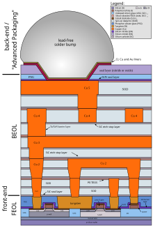
The back end of line (BEOL) is the second portion of IC fabrication where the individual devices (transistors, capacitors, resistors, etc.) get interconnected with wiring on the wafer, the metalization layer. Common metals are copper interconnect and aluminum interconnect.[1] BEOL generally begins when the first layer of metal is deposited on the wafer. BEOL includes contacts, insulating layers (dielectrics), metal levels, and bonding sites for chip-to-package connections.
After the last FEOL step, there is a wafer with isolated transistors (without any wires). In BEOL part of fabrication stage contacts (pads), interconnect wires, vias and dielectric structures are formed. For modern IC process, more than 10 metal layers can be added in the BEOL.
The process used to form DRAM capacitors creates a rough and hilly surface, which makes it difficult to add metal interconnect layers and still maintain good yield. In 1998, state-of-the-art DRAM processes had 4 metal layers, while state-of-the-art logic processes had 7 metal layers.
As of 2002, 5 or 6 layers of metal interconnect are common.
As of 2009, typical DRAM devices (1 Gbit) use 3 layers of metal interconnect, tungsten on the first layer and aluminum on the higher layers.
As of 2011, many gate arrays are available with a 3-layer interconnect. Many power ICs and analog ICs use a 3-layer interconnect.
The top-most layers of a chip have the thickest and widest and most widely separated metal layers, which make the wires on those layers have the least resistance and smallest RC time delay, so they are used for power distribution and clock distribution. The bottom-most metal layers of the chip, closest to the transistors, have thin, narrow, tightly-packed wires, used only for local interconnect. Adding layers can potentially improve performance, but adding layers also reduces yield and increases manufacturing cost.
Chips with a single metal layer typically use the polysilicon layer to "jump across" when one signal needs to cross another signal—such as the RCA CDP1802 and the 4004, giving effectively 2 layers of interconnections.
Many microprocessors were designed with two metal interconnect layers, both of them aluminum, including the 1987 CVAX and the 1989 Rigel.
Many high-performance microprocessors were designed with 3 metal interconnect layers, all of them aluminum. Those included several processors using the CMOS-3 process, including the 1992 Alpha 21064; and processors using the CMOS-6 process, including the 1996 StrongARM.
The AMD Athlon Thunderbird has 6 interconnect layers, the AMD Athlon Palomino has 7 interconnect layers, the AMD Athlon Thoroughbred A has 8 interconnect layers, and the AMD Athlon Thoroughbred B has 9 interconnect layers.[11] The Intel Xeon Dunnington has nine copper interconnect layers.[12]
Steps of the BEOL:
The four metals with the highest electrical conductivity are silver with the highest conductivity, then copper, then gold, then aluminum.
After BEOL there is a "back-end process" (also called post-fab), which is done not in the cleanroom, often by a different company. It includes wafer test, wafer backgrinding, die separation, die tests, IC packaging and final test.
After the last FEOL step, there is a wafer with isolated transistors (without any wires). In BEOL part of fabrication stage contacts (pads), interconnect wires, vias and dielectric structures are formed. For modern IC process, more than 10 metal layers can be added in the BEOL.
The process used to form DRAM capacitors creates a rough and hilly surface, which makes it difficult to add metal interconnect layers and still maintain good yield. In 1998, state-of-the-art DRAM processes had 4 metal layers, while state-of-the-art logic processes had 7 metal layers.
As of 2002, 5 or 6 layers of metal interconnect are common.
As of 2009, typical DRAM devices (1 Gbit) use 3 layers of metal interconnect, tungsten on the first layer and aluminum on the higher layers.
As of 2011, many gate arrays are available with a 3-layer interconnect. Many power ICs and analog ICs use a 3-layer interconnect.
The top-most layers of a chip have the thickest and widest and most widely separated metal layers, which make the wires on those layers have the least resistance and smallest RC time delay, so they are used for power distribution and clock distribution. The bottom-most metal layers of the chip, closest to the transistors, have thin, narrow, tightly-packed wires, used only for local interconnect. Adding layers can potentially improve performance, but adding layers also reduces yield and increases manufacturing cost.
Chips with a single metal layer typically use the polysilicon layer to "jump across" when one signal needs to cross another signal—such as the RCA CDP1802 and the 4004, giving effectively 2 layers of interconnections.
Many microprocessors were designed with two metal interconnect layers, both of them aluminum, including the 1987 CVAX and the 1989 Rigel.
Many high-performance microprocessors were designed with 3 metal interconnect layers, all of them aluminum. Those included several processors using the CMOS-3 process, including the 1992 Alpha 21064; and processors using the CMOS-6 process, including the 1996 StrongARM.
The AMD Athlon Thunderbird has 6 interconnect layers, the AMD Athlon Palomino has 7 interconnect layers, the AMD Athlon Thoroughbred A has 8 interconnect layers, and the AMD Athlon Thoroughbred B has 9 interconnect layers.[11] The Intel Xeon Dunnington has nine copper interconnect layers.[12]
Steps of the BEOL:
- Silicidation of source and drain regions and the polysilicon region.
- Adding a dielectric (first, lower layer is Pre-Metal dielectric, PMD - to isolate metal from silicon and polysilicon), CMP processing it
- Make holes in PMD, make a contacts in them.
- Add metal layer 1
- Add a second dielectric (this time it is Intra-Metal dielectric)
- Make vias through dielectric to connect lower metal with higher metal. Vias filled by Metal CVD process.
- Repeat steps 4–6 to get all metal layers.
- Add final passivation layer to protect the microchip
The four metals with the highest electrical conductivity are silver with the highest conductivity, then copper, then gold, then aluminum.
After BEOL there is a "back-end process" (also called post-fab), which is done not in the cleanroom, often by a different company. It includes wafer test, wafer backgrinding, die separation, die tests, IC packaging and final test.
CMOS fabrication process
== MA THEREFORE ART DESIGN MODERN ELECTRONIC TO PROCESS MATIC ==


