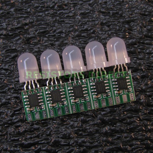
5x WS2811 Addressable RGB Pixel Bit LED Module Node 5pcs Non Waterproof USA G17
Google Pixel C tablet review: Out with the Nexus, in with the Pixel


The Pixel C comes in two storage quantities – 32GB or 64GB (with the latter priced at $100 more.
X . I Electronic circuit
An electronic circuit is composed of individual electronic components, such as resistors, transistors, capacitors, inductors and diodes, connected by conductive wires or traces through which electric current can flow. The combination of components and wires allows various simple and complex operations to be performed: signals can be amplified, computations can be performed, and data can be moved from one place to another.
Circuits can be constructed of discrete components connected by individual pieces of wire, but today it is much more common to create interconnections by photolithographic techniques on a laminated substrate (a printed circuit board or PCB) and solder the components to these interconnections to create a finished circuit. In an integrated circuit or IC, the components and interconnections are formed on the same substrate, typically a semiconductor such as silicon or (less commonly) gallium arsenide.
An electronic circuit can usually be categorized as an analog circuit, a digital circuit, or a mixed-signal circuit (a combination of analog circuits and digital circuits).
Breadboards, perfboards, and stripboards are common for testing new designs. They allow the designer to make quick changes to the circuit during development.
Analog circuits

In a series circuit, the same current passes through a series of components. A string of Christmas lights is a good example of a series circuit: if one goes out, they all do.
In a parallel circuit, all the components are connected to the same voltage, and the current divides between the various components according to their resistance.
The basic components of analog circuits are wires, resistors, capacitors, inductors, diodes, and transistors. (In 2012 it was demonstrated that memristors can be added to the list of available components.) Analog circuits are very commonly represented in schematic diagrams, in which wires are shown as lines, and each component has a unique symbol. Analog circuit analysis employs Kirchhoff's circuit laws: all the currents at a node (a place where wires meet), and the voltage around a closed loop of wires is 0. Wires are usually treated as ideal zero-voltage interconnections; any resistance or reactance is captured by explicitly adding a parasitic element, such as a discrete resistor or inductor. Active components such as transistors are often treated as controlled current or voltage sources: for example, a field-effect transistor can be modeled as a current source from the source to the drain, with the current controlled by the gate-source voltage.

When the circuit size is comparable to a wavelength of the relevant signal frequency, a more sophisticated approach must be used. Wires are treated as transmission lines, with (hopefully) constant characteristic impedance, and the impedances at the start and end determine transmitted and reflected waves on the line. Such considerations typically become important for circuit boards at frequencies above a GHz; integrated circuits are smaller and can be treated as lumped elements for frequencies less than 10GHz or so.
An alternative model is to take independent power sources and induction as basic electronic units; this allows modeling frequency dependent negative resistors, gyrators, negative impedance converters, and dependent sources as secondary electronic components
Digital circuits
In digital electronic circuits, electric signals take on discrete values, to represent logical and numeric values. These values represent the information that is being processed. In the vast majority of cases, binary encoding is used: one voltage (typically the more positive value) represents a binary '1' and another voltage (usually a value near the ground potential, 0 V) represents a binary '0'. Digital circuits make extensive use of transistors, interconnected to create logic gates that provide the functions of Boolean logic: AND, NAND, OR, NOR, XOR and all possible combinations thereof. Transistors interconnected so as to provide positive feedback are used as latches and flip flops, circuits that have two or more metastable states, and remain in one of these states until changed by an external input. Digital circuits therefore can provide both logic and memory, enabling them to perform arbitrary computational functions. (Memory based on flip-flops is known as static random-access memory (SRAM). Memory based on the storage of charge in a capacitor, dynamic random-access memory (DRAM) is also widely used.)The design process for digital circuits is fundamentally different from the process for analog circuits. Each logic gate regenerates the binary signal, so the designer need not account for distortion, gain control, offset voltages, and other concerns faced in an analog design. As a consequence, extremely complex digital circuits, with billions of logic elements integrated on a single silicon chip, can be fabricated at low cost. Such digital integrated circuits are ubiquitous in modern electronic devices, such as calculators, mobile phone handsets, and computers. As digital circuits become more complex, issues of time delay, logic races, power dissipation, non-ideal switching, on-chip and inter-chip loading, and leakage currents, become limitations to the density, speed and performance.
Digital circuitry is used to create general purpose computing chips, such as microprocessors, and custom-designed logic circuits, known as application-specific integrated circuit (ASICs). Field-programmable gate arrays (FPGAs), chips with logic circuitry whose configuration can be modified after fabrication, are also widely used in prototyping and development.
Mixed-signal circuits
Mixed-signal or hybrid circuits contain elements of both analog and digital circuits. Examples include comparators, timers, phase-locked loops, analog-to-digital converters, and digital-to-analog converters. Most modern radio and communications circuitry uses mixed signal circuits. For example, in a receiver, analog circuitry is used to amplify and frequency-convert signals so that they reach a suitable state to be converted into digital values, after which further signal processing can be performed in the digital domain.
Electronic circuit design comprises the analysis and synthesis of electronic circuits
Methods
To design any electrical circuit, either analog or digital, electrical engineers need to be able to predict the voltages and currents at all places within the circuit. Linear circuits, that is, circuits wherein the outputs are linearly dependent on the inputs, can be analyzed by hand using complex analysis. Simple nonlinear circuits can also be analyzed in this way. Specialized software has been created to analyze circuits that are either too complicated or too nonlinear to analyze by hand.Circuit simulation software allows engineers to design circuits more efficiently, reducing the time cost and risk of error involved in building circuit prototypes. Some of these make use of hardware description languages such as VHDL or Verilog.
Network simulation software
More complex circuits are analyzed with circuit simulation software such as SPICE and EMTP.Linearization around operating point
When faced with a new circuit, the software first tries to find a steady state solution wherein all the nodes conform to Kirchhoff's Current Law and the voltages across and through each element of the circuit conform to the voltage/current equations governing that element.Once the steady state solution is found, the software can analyze the response to perturbations using piecewise approximation, harmonic balance or other methods.
Piece-wise linear approximation
Software such as the PLECS interface to Simulink uses piecewise linear approximation of the equations governing the elements of a circuit. The circuit is treated as a completely linear network of ideal diodes. Every time a diode switches from on to off or vice versa, the configuration of the linear network changes. Adding more detail to the approximation of equations increases the accuracy of the simulation, but also increases its running time.Synthesis
Simple circuits may be designed by connecting a number of elements or functional blocks such as integrated circuits.More complex digital circuits are typically designed with the aid of computer software. Logic circuits (and sometimes mixed mode circuits) are often described in such hardware description languages as HDL, VHDL or Verilog, then synthesized using a logic synthesis engine.
X . II Digital electronics
Digital electronics or digital (electronic) circuits are electronics that operate on digital signals. In contrast, analog circuits manipulate analog signals whose performance is more subject to manufacturing tolerance, signal attenuation and noise. Digital techniques are helpful because it is a lot easier to get an electronic device to switch into one of a number of known states than to accurately reproduce a continuous range of values.
Digital electronic circuits are usually made from large assemblies of logic gates (often printed on integrated circuits), simple electronic representations of Boolean logic functions
Digital electronics

A digital signal has two or more distinguishable waveforms, in this example, high voltage and low voltages, each of which can be mapped onto a digit.

An industrial digital controller
An advantage of digital circuits when compared to analog circuits is that signals represented digitally can be transmitted without degradation due to noise.[8] For example, a continuous audio signal transmitted as a sequence of 1s and 0s, can be reconstructed without error, provided the noise picked up in transmission is not enough to prevent identification of the 1s and 0s. An hour of music can be stored on a compact disc using about 6 billion binary digits.
In a digital system, a more precise representation of a signal can be obtained by using more binary digits to represent it. While this requires more digital circuits to process the signals, each digit is handled by the same kind of hardware, resulting in an easily scalable system. In an analog system, additional resolution requires fundamental improvements in the linearity and noise characteristics of each step of the signal chain.
Computer-controlled digital systems can be controlled by software, allowing new functions to be added without changing hardware. Often this can be done outside of the factory by updating the product's software. So, the product's design errors can be corrected after the product is in a customer's hands.
Information storage can be easier in digital systems than in analog ones. The noise-immunity of digital systems permits data to be stored and retrieved without degradation. In an analog system, noise from aging and wear degrade the information stored. In a digital system, as long as the total noise is below a certain level, the information can be recovered perfectly.
Even when more significant noise is present, the use of redundancy permits the recovery of the original data provided too many errors do not occur.
In some cases, digital circuits use more energy than analog circuits to accomplish the same tasks, thus producing more heat which increases the complexity of the circuits such as the inclusion of heat sinks. In portable or battery-powered systems this can limit use of digital systems.
For example, battery-powered cellular telephones often use a low-power analog front-end to amplify and tune in the radio signals from the base station. However, a base station has grid power and can use power-hungry, but very flexible software radios. Such base stations can be easily reprogrammed to process the signals used in new cellular standards.
Digital circuits are sometimes more expensive, especially in small quantities.
Most useful digital systems must translate from continuous analog signals to discrete digital signals. This causes quantization errors. Quantization error can be reduced if the system stores enough digital data to represent the signal to the desired degree of fidelity. The Nyquist-Shannon sampling theorem provides an important guideline as to how much digital data is needed to accurately portray a given analog signal.
In some systems, if a single piece of digital data is lost or misinterpreted, the meaning of large blocks of related data can completely change. Because of the cliff effect, it can be difficult for users to tell if a particular system is right on the edge of failure, or if it can tolerate much more noise before failing.
Digital fragility can be reduced by designing a digital system for robustness. For example, a parity bit or other error management method can be inserted into the signal path. These schemes help the system detect errors, and then either correct the errors, or at least ask for a new copy of the data. In a state-machine, the state transition logic can be designed to catch unused states and trigger a reset sequence or other error recovery routine.
Digital memory and transmission systems can use techniques such as error detection and correction to use additional data to correct any errors in transmission and storage.
On the other hand, some techniques used in digital systems make those systems more vulnerable to single-bit errors. These techniques are acceptable when the underlying bits are reliable enough that such errors are highly unlikely.
A single-bit error in audio data stored directly as linear pulse code modulation (such as on a CD-ROM) causes, at worst, a single click. Instead, many people use audio compression to save storage space and download time, even though a single-bit error may corrupt the entire song.
Construction

Integrated circuits consist of multiple transistors on one silicon chip, and are the least expensive way to make large number of interconnected logic gates. Integrated circuits are usually designed by engineers using electronic design automation software (see below for more information) to perform some type of function.
Integrated circuits are usually interconnected on a printed circuit board which is a board which holds electrical components, and connects them together with copper traces.
Design
Each logic symbol is represented by a different shape. The actual set of shapes was introduced in 1984 under IEEE/ANSI standard 91-1984. "The logic symbol given under this standard are being increasingly used now and have even started appearing in the literature published by manufacturers of digital integrated circuits."[9]Another form of digital circuit is constructed from lookup tables, (many sold as "programmable logic devices", though other kinds of PLDs exist). Lookup tables can perform the same functions as machines based on logic gates, but can be easily reprogrammed without changing the wiring. This means that a designer can often repair design errors without changing the arrangement of wires. Therefore, in small volume products, programmable logic devices are often the preferred solution. They are usually designed by engineers using electronic design automation software.
When the volumes are medium to large, and the logic can be slow, or involves complex algorithms or sequences, often a small microcontroller is programmed to make an embedded system. These are usually programmed by software engineers.
When only one digital circuit is needed, and its design is totally customized, as for a factory production line controller, the conventional solution is a programmable logic controller, or PLC. These are usually programmed by electricians, using ladder logic.
Structure of digital systems
Engineers use many methods to minimize logic functions, in order to reduce the circuit's complexity. When the complexity is less, the circuit also has fewer errors and less electronics, and is therefore less expensive.The most widely used simplification is a minimization algorithm like the Espresso heuristic logic minimizer within a CAD system, although historically, binary decision diagrams, an automated Quine–McCluskey algorithm, truth tables, Karnaugh maps, and Boolean algebra have been used.
Representation
Representations are crucial to an engineer's design of digital circuits. Some analysis methods only work with particular representations.The classical way to represent a digital circuit is with an equivalent set of logic gates. Another way, often with the least electronics, is to construct an equivalent system of electronic switches (usually transistors). One of the easiest ways is to simply have a memory containing a truth table. The inputs are fed into the address of the memory, and the data outputs of the memory become the outputs.
For automated analysis, these representations have digital file formats that can be processed by computer programs. Most digital engineers are very careful to select computer programs ("tools") with compatible file formats.
Combinational vs. Sequential
To choose representations, engineers consider types of digital systems. Most digital systems divide into "combinational systems" and "sequential systems." A combinational system always presents the same output when given the same inputs. It is basically a representation of a set of logic functions, as already discussed.A sequential system is a combinational system with some of the outputs fed back as inputs. This makes the digital machine perform a "sequence" of operations. The simplest sequential system is probably a flip flop, a mechanism that represents a binary digit or "bit".
Sequential systems are often designed as state machines. In this way, engineers can design a system's gross behavior, and even test it in a simulation, without considering all the details of the logic functions.
Sequential systems divide into two further subcategories. "Synchronous" sequential systems change state all at once, when a "clock" signal changes state. "Asynchronous" sequential systems propagate changes whenever inputs change. Synchronous sequential systems are made of well-characterized asynchronous circuits such as flip-flops, that change only when the clock changes, and which have carefully designed timing margins.
Synchronous systems

The state register is just a representation of a binary number. If the states in the state machine are numbered (easy to arrange), the logic function is some combinational logic that produces the number of the next state.
Asynchronous systems
As of 2014, most digital logic is synchronous because it is easier to create and verify a synchronous design. However, asynchronous logic is thought can be superior because its speed is not constrained by an arbitrary clock; instead, it runs at the maximum speed of its logic gates. Building an asynchronous system using faster parts makes the circuit faster.Nevertherless, most systems need circuits that allow external unsynchronized signals to enter synchronous logic circuits. These are inherently asynchronous in their design and must be analyzed as such. Examples of widely used asynchronous circuits include synchronizer flip-flops, switch debouncers and arbiters.
Asynchronous logic components can be hard to design because all possible states, in all possible timings must be considered. The usual method is to construct a table of the minimum and maximum time that each such state can exist, and then adjust the circuit to minimize the number of such states. Then the designer must force the circuit to periodically wait for all of its parts to enter a compatible state (this is called "self-resynchronization"). Without such careful design, it is easy to accidentally produce asynchronous logic that is "unstable," that is, real electronics will have unpredictable results because of the cumulative delays caused by small variations in the values of the electronic components.
Register transfer systems
In register transfer logic, binary numbers are stored in groups of flip flops called registers. The outputs of each register are a bundle of wires called a "bus" that carries that number to other calculations. A calculation is simply a piece of combinational logic. Each calculation also has an output bus, and these may be connected to the inputs of several registers. Sometimes a register will have a multiplexer on its input, so that it can store a number from any one of several buses. Alternatively, the outputs of several items may be connected to a bus through buffers that can turn off the output of all of the devices except one. A sequential state machine controls when each register accepts new data from its input.
Asynchronous register-transfer systems (such as computers) have a general solution. In the 1980s, some researchers discovered that almost all synchronous register-transfer machines could be converted to asynchronous designs by using first-in-first-out synchronization logic. In this scheme, the digital machine is characterized as a set of data flows. In each step of the flow, an asynchronous "synchronization circuit" determines when the outputs of that step are valid, and presents a signal that says, "grab the data" to the stages that use that stage's inputs. It turns out that just a few relatively simple synchronization circuits are needed.
Computer design

In this way, the complex task of designing the controls of a computer is reduced to a simpler task of programming a collection of much simpler logic machines.
Almost all computers are synchronous. However, true asynchronous computers have also been designed. One example is the Aspida DLX core.[10] Another was offered by ARM Holdings. Speed advantages have not materialized, because modern computer designs already run at the speed of their slowest component, usually memory. These do use somewhat less power because a clock distribution network is not needed. An unexpected advantage is that asynchronous computers do not produce spectrally-pure radio noise, so they are used in some mobile-phone base-station controllers. They may be more secure in cryptographic applications because their electrical and radio emissions can be more difficult to decode.
Computer architecture is a specialized engineering activity that tries to arrange the registers, calculation logic, buses and other parts of the computer in the best way for some purpose. Computer architects have applied large amounts of ingenuity to computer design to reduce the cost and increase the speed and immunity to programming errors of computers. An increasingly common goal is to reduce the power used in a battery-powered computer system, such as a cell-phone. Many computer architects serve an extended apprenticeship as microprogrammers.
Digital circuits are made from analog components. The design must assure that the analog nature of the components doesn't dominate the desired digital behavior. Digital systems must manage noise and timing margins, parasitic inductances and capacitances, and filter power connections.
Bad designs have intermittent problems such as "glitches", vanishingly fast pulses that may trigger some logic but not others, "runt pulses" that do not reach valid "threshold" voltages, or unexpected ("undecoded") combinations of logic states.
Additionally, where clocked digital systems interface to analog systems or systems that are driven from a different clock, the digital system can be subject to metastability where a change to the input violates the set-up time for a digital input latch. This situation will self-resolve, but will take a random time, and while it persists can result in invalid signals being propagated within the digital system for a short time.
Since digital circuits are made from analog components, digital circuits calculate more slowly than low-precision analog circuits that use a similar amount of space and power. However, the digital circuit will calculate more repeatably, because of its high noise immunity. On the other hand, in the high-precision domain (for example, where 14 or more bits of precision are needed), analog circuits require much more power and area than digital equivalents.
Automated design tools
To save costly engineering effort, much of the effort of designing large logic machines has been automated. The computer programs are called "electronic design automation tools" or just "EDA."Simple truth table-style descriptions of logic are often optimized with EDA that automatically produces reduced systems of logic gates or smaller lookup tables that still produce the desired outputs. The most common example of this kind of software is the Espresso heuristic logic minimizer.
Most practical algorithms for optimizing large logic systems use algebraic manipulations or binary decision diagrams, and there are promising experiments with genetic algorithms and annealing optimizations.
To automate costly engineering processes, some EDA can take state tables that describe state machines and automatically produce a truth table or a function table for the combinational logic of a state machine. The state table is a piece of text that lists each state, together with the conditions controlling the transitions between them and the belonging output signals.
It is common for the function tables of such computer-generated state-machines to be optimized with logic-minimization software such as Minilog.
Often, real logic systems are designed as a series of sub-projects, which are combined using a "tool flow." The tool flow is usually a "script," a simplified computer language that can invoke the software design tools in the right order.
Tool flows for large logic systems such as microprocessors can be thousands of commands long, and combine the work of hundreds of engineers.
Writing and debugging tool flows is an established engineering specialty in companies that produce digital designs. The tool flow usually terminates in a detailed computer file or set of files that describe how to physically construct the logic. Often it consists of instructions to draw the transistors and wires on an integrated circuit or a printed circuit board.
Parts of tool flows are "debugged" by verifying the outputs of simulated logic against expected inputs. The test tools take computer files with sets of inputs and outputs, and highlight discrepancies between the simulated behavior and the expected behavior.
Once the input data is believed correct, the design itself must still be verified for correctness. Some tool flows verify designs by first producing a design, and then scanning the design to produce compatible input data for the tool flow. If the scanned data matches the input data, then the tool flow has probably not introduced errors.
The functional verification data are usually called "test vectors". The functional test vectors may be preserved and used in the factory to test that newly constructed logic works correctly. However, functional test patterns don't discover common fabrication faults. Production tests are often designed by software tools called "test pattern generators". These generate test vectors by examining the structure of the logic and systematically generating tests for particular faults. This way the fault coverage can closely approach 100%, provided the design is properly made testable (see next section).
Once a design exists, and is verified and testable, it often needs to be processed to be manufacturable as well. Modern integrated circuits have features smaller than the wavelength of the light used to expose the photoresist. Manufacturability software adds interference patterns to the exposure masks to eliminate open-circuits, and enhance the masks' contrast.
Design for testability
There are several reasons for testing a logic circuit. When the circuit is first developed, it is necessary to verify that the design circuit meets the required functional and timing specifications. When multiple copies of a correctly designed circuit are being manufactured, it is essential to test each copy to ensure that the manufacturing process has not introduced any flaws.[12]A large logic machine (say, with more than a hundred logical variables) can have an astronomical number of possible states. Obviously, in the factory, testing every state is impractical if testing each state takes a microsecond, and there are more states than the number of microseconds since the universe began. Unfortunately, this ridiculous-sounding case is typical.
Fortunately, large logic machines are almost always designed as assemblies of smaller logic machines. To save time, the smaller sub-machines are isolated by permanently installed "design for test" circuitry, and are tested independently.
One common test scheme known as "scan design" moves test bits serially (one after another) from external test equipment through one or more serial shift registers known as "scan chains". Serial scans have only one or two wires to carry the data, and minimize the physical size and expense of the infrequently used test logic.
After all the test data bits are in place, the design is reconfigured to be in "normal mode" and one or more clock pulses are applied, to test for faults (e.g. stuck-at low or stuck-at high) and capture the test result into flip-flops and/or latches in the scan shift register(s). Finally, the result of the test is shifted out to the block boundary and compared against the predicted "good machine" result.
In a board-test environment, serial to parallel testing has been formalized with a standard called "JTAG" (named after the "Joint Test Action Group" that made it).
Another common testing scheme provides a test mode that forces some part of the logic machine to enter a "test cycle." The test cycle usually exercises large independent parts of the machine.
Trade-offs
Several numbers determine the practicality of a system of digital logic: cost, reliability, fanout and speed. Engineers explored numerous electronic devices to get a favourable combination of these personalities.Cost
The cost of a logic gate is crucial, primarily because very many gates are needed to build a computer or other advanced digital system and because the more gates can be used, the more able and/or respondent the machine can become. Since the bulk of a digital computer is simply an interconnected network of logic gates, the overall cost of building a computer correlates strongly with the price per logic gate. In the 1930s, the earliest digital logic systems were constructed from telephone relays because these were inexpensive and relatively reliable. After that, electrical engineers always used the cheapest available electronic switches that could still fulfill the requirements.The earliest integrated circuits were a happy accident. They were constructed not to save money, but to save weight, and permit the Apollo Guidance Computer to control an inertial guidance system for a spacecraft. The first integrated circuit logic gates cost nearly $50 (in 1960 dollars, when an engineer earned $10,000/year). To everyone's surprise, by the time the circuits were mass-produced, they had become the least-expensive method of constructing digital logic. Improvements in this technology have driven all subsequent improvements in cost.
With the rise of integrated circuits, reducing the absolute number of chips used represented another way to save costs. The goal of a designer is not just to make the simplest circuit, but to keep the component count down. Sometimes this results in more complicated designs with respect to the underlying digital logic but nevertheless reduces the number of components, board size, and even power consumption. A major motive for reducing component count on printed circuit boards is to reduce the manufacturing defect rate and increase reliability, as every soldered connection is a potentially bad one, so the defect and failure rates tend to increase along with the total number of component pins.
For example, in some logic families, NAND gates are the simplest digital gate to build. All other logical operations can be implemented by NAND gates. If a circuit already required a single NAND gate, and a single chip normally carried four NAND gates, then the remaining gates could be used to implement other logical operations like logical and. This could eliminate the need for a separate chip containing those different types of gates.
Reliability
The "reliability" of a logic gate describes its mean time between failure (MTBF). Digital machines often have millions of logic gates. Also, most digital machines are "optimized" to reduce their cost. The result is that often, the failure of a single logic gate will cause a digital machine to stop working. It is possible to design machines to be more reliable by using redundant logic which will not malfunction as a result of the failure of any single gate (or even any two, three, or four gates), but this necessarily entails using more components, which raises the financial cost and also usually increases the weight of the machine and may increase the power it consumes.Digital machines first became useful when the MTBF for a switch got above a few hundred hours. Even so, many of these machines had complex, well-rehearsed repair procedures, and would be nonfunctional for hours because a tube burned-out, or a moth got stuck in a relay. Modern transistorized integrated circuit logic gates have MTBFs greater than 82 billion hours (8.2 · 1010 hours),[13] and need them because they have so many logic gates.
Fanout
Fanout describes how many logic inputs can be controlled by a single logic output without exceeding the electrical current ratings of the gate outputs.[14] The minimum practical fanout is about five. Modern electronic logic gates using CMOS transistors for switches have fanouts near fifty, and can sometimes go much higher.Speed
The "switching speed" describes how many times per second an inverter (an electronic representation of a "logical not" function) can change from true to false and back. Faster logic can accomplish more operations in less time. Digital logic first became useful when switching speeds got above 50 Hz, because that was faster than a team of humans operating mechanical calculators. Modern electronic digital logic routinely switches at 5 GHz (5 · 109 Hz), and some laboratory systems switch at more than 1 THz (1 · 1012 Hz).Logic families
Design started with relays. Relay logic was relatively inexpensive and reliable, but slow. Occasionally a mechanical failure would occur. Fanouts were typically about 10, limited by the resistance of the coils and arcing on the contacts from high voltages.Later, vacuum tubes were used. These were very fast, but generated heat, and were unreliable because the filaments would burn out. Fanouts were typically 5...7, limited by the heating from the tubes' current. In the 1950s, special "computer tubes" were developed with filaments that omitted volatile elements like silicon. These ran for hundreds of thousands of hours.
The first semiconductor logic family was resistor–transistor logic. This was a thousand times more reliable than tubes, ran cooler, and used less power, but had a very low fan-in of 3. Diode–transistor logic improved the fanout up to about 7, and reduced the power. Some DTL designs used two power-supplies with alternating layers of NPN and PNP transistors to increase the fanout.
Transistor–transistor logic (TTL) was a great improvement over these. In early devices, fanout improved to 10, and later variations reliably achieved 20. TTL was also fast, with some variations achieving switching times as low as 20 ns. TTL is still used in some designs.
Emitter coupled logic is very fast but uses a lot of power. It was extensively used for high-performance computers made up of many medium-scale components (such as the Illiac IV).
By far, the most common digital integrated circuits built today use CMOS logic, which is fast, offers high circuit density and low-power per gate. This is used even in large, fast computers, such as the IBM System z.
Recent developments
In 2009, researchers discovered that memristors can implement a boolean state storage (similar to a flip flop, implication and logical inversion), providing a complete logic family with very small amounts of space and power, using familiar CMOS semiconductor processes.The discovery of superconductivity has enabled the development of rapid single flux quantum (RSFQ) circuit technology, which uses Josephson junctions instead of transistors. Most recently, attempts are being made to construct purely optical computing systems capable of processing digital information using nonlinear optical elements.
X . III Integrated circuit design
Integrated circuit design, or IC design, is a subset of electronics engineering, encompassing the particular logic and circuit design techniques required to design integrated circuits, or ICs. ICs consist of miniaturized electronic components built into an electrical network on a monolithic semiconductor substrate by photolithography.
IC design can be divided into the broad categories of digital and analog IC design. Digital IC design is to produce components such as microprocessors, FPGAs, memories (RAM, ROM, and flash) and digital ASICs. Digital design focuses on logical correctness, maximizing circuit density, and placing circuits so that clock and timing signals are routed efficiently. Analog IC design also has specializations in power IC design and RF IC design. Analog IC design is used in the design of op-amps, linear regulators, phase locked loops, oscillators and active filters. Analog design is more concerned with the physics of the semiconductor devices such as gain, matching, power dissipation, and resistance. Fidelity of analog signal amplification and filtering is usually critical and as a result, analog ICs use larger area active devices than digital designs and are usually less dense in circuitry.
Modern ICs are enormously complicated. An average desktop computer chip, as of 2015, has over 1 billion transistors. The rules for what can and cannot be manufactured are also extremely complex. Common IC processes of 2015 have more than 500 rules. Furthermore, since the manufacturing process itself is not completely predictable, designers must account for its statistical nature. The complexity of modern IC design, as well as market pressure to produce designs rapidly, has led to the extensive use of automated design tools in the IC design process. In short, the design of an IC using EDA software is the design, test, and verification of the instructions that the IC is to carry out.

Layout view of a simple CMOS Operational Amplifier (inputs are to the left and the compensation capacitor is to the right). The metal layer is coloured blue, green and brown are N- and P-doped Si, the polysilicon is red and vias are crosses
Fundamentals
Integrated circuit design involves the creation of electronic components, such as transistors, resistors, capacitors and the metallic interconnect of these components onto a piece of semiconductor, typically silicon. A method to isolate the individual components formed in the substrate is necessary since the substrate silicon is conductive and often forms an active region of the individual components. The two common methods are p-n junction isolation and dielectric isolation. Attention must be given to power dissipation of transistors and interconnect resistances and current density of the interconnect, contacts and vias since ICs contain very tiny devices compared to discrete components, where such concerns are less of an issue. Electromigration in metallic interconnect and ESD damage to the tiny components are also of concern. Finally, the physical layout of certain circuit subblocks is typically critical, in order to achieve the desired speed of operation, to segregate noisy portions of an IC from quiet portions, to balance the effects of heat generation across the IC, or to facilitate the placement of connections to circuitry outside the IC.Design steps
A typical IC design cycle involves several steps:
- Feasibility study and die size estimate
- Function analysis
- System Level Design
- Analogue Design, Simulation & Layout
- Digital Design, Simulation & Synthesis
- System Simulation & Verification
- Design For Test and Automatic test pattern generation
- Design for manufacturability (IC)
- Tape-in
- Mask data preparation
- Tape-out
- Wafer fabrication
- Die test
- Packaging
- Post silicon validation and integration
- Device characterization
- Tweak (if necessary)
- Datasheet generation (of usually a Portable Document Format (PDF) file)
- Ramp up
- Production
- Yield Analysis / Warranty Analysis Reliability (semiconductor)
- Failure analysis on any returns
- Plan for next generation chip using production information if possible
- Electronic system-level design: This step creates the user functional specification. The user may use a variety of languages and tools to create this description. Examples include a C/C++ model, SystemC, SystemVerilog Transaction Level Models, Simulink and MATLAB.
- RTL design: This step converts the user specification (what the user wants the chip to do) into a register transfer level (RTL) description. The RTL describes the exact behavior of the digital circuits on the chip, as well as the interconnections to inputs and outputs.
- Physical design: This step takes the RTL, and a library of available logic gates, and creates a chip design. This involves figuring out which gates to use, defining places for them, and wiring them together.
Design process
Microarchitecture and system-level design
The initial chip design process begins with system-level design and microarchitecture planning. Within IC design companies, management and often analytics will draft a proposal for a design team to start the design of a new chip to fit into an industry segment. Upper-level designers will meet at this stage to decide how the chip will operate functionally. This step is where an IC's functionality and design are decided. IC designers will map out the functional requirements, verification testbenches, and testing methodologies for the whole project, and will then turn the preliminary design into a system-level specification that can be simulated with simple models using languages like C++ and MATLAB and emulation tools. For pure and new designs, the system design stage is where an Instruction set and operation is planned out, and in most chips existing instruction sets are modified for newer functionality. Design at this stage is often statements such as encodes in the MP3 format or implements IEEE floating-point arithmetic. At later stages in the design process, each of these innocent looking statements expands to hundreds of pages of textual documentation.RTL design
Upon agreement of a system design, RTL designers then implement the functional models in a hardware description language like Verilog, SystemVerilog, or VHDL. Using digital design components like adders, shifters, and state machines as well as computer architecture concepts like pipelining, superscalar execution, and branch prediction, RTL designers will break a functional description into hardware models of components on the chip working together. Each of the simple statements described in the system design can easily turn into thousands of lines of RTL code, which is why it is extremely difficult to verify that the RTL will do the right thing in all the possible cases that the user may throw at it.To reduce the number of functionality bugs, a separate hardware verification group will take the RTL and design testbenches and systems to check that the RTL actually is performing the same steps under many different conditions, classified as the domain of functional verification. Many techniques are used, none of them perfect but all of them useful – extensive logic simulation, formal methods, hardware emulation, lint-like code checking, code coverage, and so on.
A tiny error here can make the whole chip useless, or worse. The famous Pentium FDIV bug caused the results of a division to be wrong by at most 61 parts per million, in cases that occurred very infrequently. No one even noticed it until the chip had been in production for months. Yet Intel was forced to offer to replace, for free, every chip sold until they could fix the bug, at a cost of $475 million (US).[citation needed]
Physical design
RTL is only a behavioral model of the actual functionality of what the chip is supposed to operate under. It has no link to a physical aspect of how the chip would operate in real life at the materials, physics, and electrical engineering side. For this reason, the next step in the IC design process, physical design stage, is to map the RTL into actual geometric representations of all electronics devices, such as capacitors, resistors, logic gates, and transistors that will go on the chip.
The main steps of physical design are listed below. In practice there is not a straightforward progression - considerable iteration is required to ensure all objectives are met simultaneously. This is a difficult problem in its own right, called design closure.
- Logic synthesis: The RTL is mapped into a gate-level netlist in the target technology of the chip.
- Floorplanning: The RTL of the chip is assigned to gross regions of the chip, input/output (I/O) pins are assigned and large objects (arrays, cores, etc.) are placed.
- Placement: The gates in the netlist are assigned to nonoverlapping locations on the die area.
- Logic/placement refinement: Iterative logical and placement transformations to close performance and power constraints.
- Clock insertion: Clock signal wiring is (commonly, clock trees) introduced into the design.
- Routing: The wires that connect the gates in the netlist are added.
- Postwiring optimization: Performance (timing closure), noise (signal integrity), and yield (Design for manufacturability) violations are removed.
- Design for manufacturability: The design is modified, where possible, to make it as easy and efficient as possible to produce. This is achieved by adding extra vias or adding dummy metal/diffusion/poly layers wherever possible while complying to the design rules set by the foundry.
- Final checking: Since errors are expensive, time consuming and hard to spot, extensive error checking is the rule, making sure the mapping to logic was done correctly, and checking that the manufacturing rules were followed faithfully.
- Tapeout and mask generation: the design data is turned into photomasks in mask data preparation.
Analog design
Before the advent of the microprocessor and software based design tools, analog ICs were designed using hand calculations and process kit parts. These ICs were low complexity circuits, for example, op-amps, usually involving no more than ten transistors and few connections. An iterative trial-and-error process and "overengineering" of device size was often necessary to achieve a manufacturable IC. Reuse of proven designs allowed progressively more complicated ICs to be built upon prior knowledge. When inexpensive computer processing became available in the 1970s, computer programs were written to simulate circuit designs with greater accuracy than practical by hand calculation. The first circuit simulator for analog ICs was called SPICE (Simulation Program with Integrated Circuits Emphasis). Computerized circuit simulation tools enable greater IC design complexity than hand calculations can achieve, making the design of analog ASICs practical. The computerized circuit simulators also enable mistakes to be found early in the design cycle before a physical device is fabricated. Additionally, a computerized circuit simulator can implement more sophisticated device models and circuit analysis too tedious for hand calculations, permitting Monte Carlo analysis and process sensitivity analysis to be practical. The effects of parameters such as temperature variation, doping concentration variation and statistical process variations can be simulated easily to determine if an IC design is manufacturable. Overall, computerized circuit simulation enables a higher degree of confidence that the circuit will work as expected upon manufacture.Coping with variability
A challenge most critical to analog IC design involves the variability of the individual devices built on the semiconductor chip. Unlike board-level circuit design which permits the designer to select devices that have each been tested and binned according to value, the device values on an IC can vary widely which are uncontrollable by the designer. For example, some IC resistors can vary ±20% and β of an integrated BJT can vary from 20 to 100. In the latest CMOS processes, β of vertical PNP transistors can even go below 1. To add to the design challenge, device properties often vary between each processed semiconductor wafer. Device properties can even vary significantly across each individual IC due to doping gradients. The underlying cause of this variability is that many semiconductor devices are highly sensitive to uncontrollable random variances in the process. Slight changes to the amount of diffusion time, uneven doping levels, etc. can have large effects on device properties.Some design techniques used to reduce the effects of the device variation are:
- Using the ratios of resistors, which do match closely, rather than absolute resistor value.
- Using devices with matched geometrical shapes so they have matched variations.
- Making devices large so that statistical variations becomes an insignificant fraction of the overall device property.
- Segmenting large devices, such as resistors, into parts and interweaving them to cancel variations.
- Using common centroid device layout to cancel variations in devices which must match closely (such as the transistor differential pair of an op amp).
Vendors
The three largest companies selling electronic design automation tools are Synopsys, Cadence, and Mentor Graphics.X . IIII Digital information - bits, bytes and pixels.
a Bit
1 A bit is an irreducible discrete unit of information used by computers.
o It can have two different values or "settings."
o It be thought of as an on-off switch.
ü In this case, the two possible settings are "on" or "off".
o It can also be thought of as a yes-no instruction.
ü In this case, the two possible values are "yes" or "no".
o It can be represented by the digits 0 or 1
ü In this case, the two possible values are 1 or 0
2 A set or ordered "stream" of bits can be used to carry complex information
b Binary numbers
o A set of bits can be thought of as a representation of a "binary" number, which is another way of representing familiar (base 10) numbers, as discussed in class. Examples:
ü 00 (binary number for 0)
ü 01 (binary number for 1)
ü 10 (binary number for 2)
ü 11 (binary number for 3)
c Byte
1 A byte is an ordered set of 8 bits having given values
2 A byte can have any one of 256 "values," depending on the values (e.g., 0 or 1) of each of its 8 bits.
o Examples of different values of a byte are:
ü 00000000 (binary number for 0)
ü 00000001 (binary number for 1)
ü 00000010 (binary number for 2)
ü .....
ü 11001000 (binary for 208)
ü .....
ü 11111111 (binary number for 255)
o The reason there are 256 values is that there are 256 different 8 digit "binary numbers" made up out of 0's and 1's only. Mathematically,
ü 256 = (# of values of each bit)(# of bits) = 28 = 2 x 2 x 2 x 2 x 2 x 2 x 2 x 2.
o The value of a byte, therefore, can be ordered from 0 to 255.
3 A Megabyte is a million bytes.
o Each of the bytes can have any one of the 256 values.
o Computer memory and information storage capability is measured in Megabytes
d The ASCII character set
1 ASCII stands for the American Standard Code for Information Interchange.
2 There are 256 characters in the ASCII character set.
o These characters include all of the lower and upper case letters of the alphabet.
o The standard typewriter characters, such as @, $,& , etc. are also included in the ASCII set.
3 Each of these different characters is represented by a different byte, according to a specific permanently agreed upon convention.
o Examples:
ü A = character #65 (byte value 01000001)
ü d = character #100 (byte value 01100100)
ü @ = character #65 (byte value 01000000)
4 Hence, a Megabyte of computer memory can hold a million characters (including spaces between words).
e Pixel
1 A pixel is an irreducible discrete unit of information in an image or picture.
o Pixel stands for "picture element."
o In a "mosaic," a picture is made up of discrete colored tiles. Each tile is a pixel. The value of each pixel is its color.
o The "pointillist" artist, George Seurat, used dots of color as pixels. It is often convenient to think of pixels as dots of color (or grey-scale values).
o TV screens examined closely will be found to consist of dots of color (pixels).
o All images can be "digitized" into pixels by using digitizing instruments, such as scanners.
2 The location of a pixel is given by an x-y coordinate on a graph.
f Bitmap images and color digital photos.
1 Any bitmapped image can be represented by giving the locations and values of all its pixels.
o A "map" of locations and values of pixels is called a bitmap.
o An image described by a bitmap is called a bitmapped image.
o A digital photo is an example of a bitmapped image.
2 The depth of a pixel in a digital photo seen on a computer screen is determined by the number of bits of information it contains.
o The appearance and quality of a digital photo seen on the computer screen is determined by the depth of the pixels.
o A 1 bit pixel can take on 21 = 2 different values, 0 or 1 (dot is off or on)
ü Usually the dot is white, so this means the color of a 1 bit pixel is black or white
ü Note, in Photoshop language, a bitmapped image is alway made up of 1 bit pixels, whereas in more general usage a bitmapped image can be made up of pixels of arbitrary depth
ü Show using Photoshop mode how a color image looks in 1 bit mode. Show pixels (simulated)
o A 2 bit pixel can take on 22 = 4 different values corresponding to a two digit binary number.
ü These values are 00, 01, 10, and 11.
ü For example, these values can trigger black, white, and two shades of gray.
o A 3 bit pixel can take on 23 = 8 different values.
ü For example, the values can trigger black, white and 6 different colors.
o An n-bit pixel can take on 2n different values.
ü In simple language, multiply 2 times itself a total of n times: 2 x 2 x 2 x ... (n factors of 2)
o A computer set to show 8-bit color has 8-bit pixels, and can display images with 28 = 256 colors. A color scheme using 256 colors is sometimes called in dexed color.
ü Later we will show what a color image looks like in 8 bit color using the Photoshop mode indexed color.
o A computer set to show 16-bit color, has 16-bit pixels and displays images with 216 = 32,768 colors
o These days, most laptops can show 24-bit color (also known as RGB color, with 8 bits (1 byte) describing the brightness of each primary)
ü An image in 24-bit color can show 224 = (over 16 million) different colors. (Check with your calculators)
ü See the section of Physics 2000 under Color TV's dealing with partitive mixing to see one way this works.
II Networking
a The Internet (the Net)
1 An all-encompasing term that describes a complex interconnection of international computer-information networks.
o Domains identify unique top-level Net addresses.
ü In the email address goldman@spot.colorado .edu, the domain is edu.
o Subdomains organize the network structure within a domain
ü In the above email address the subdomain is colorado.
o As we shall see later, spot is the name of the server in that subdomain
2 Information travels between 2 (often distant) computers by unpredictable routes.
o The communication occurs over wires, telephone, fiber-optic and other special cables, but also over satellite links to radar dishes hooked up to computers by cables.
o The route was deliberately made unpredictable in the earliest version ot the Internet
ü The ArpaNet (in the 1960's) was designed to be hard to destroy in a potential war, by using automatic switching to choose the best of a variety of different "routes" between the computers.
ü There is an analogy between this aspect of the Net and blood vessels carrying blood: If some paths are damaged or blocked, the blood takes another path.
3 Typically, one computer contains files of bits or bytes, while the other receives copies of the files which it decodes and displays as words, pictures, etc.
o This requires special software on each computer.
ü The computer containing the original file is called the HOST.
ü The remote computer is sometimes called the DESKTOP or the USER.
o The SERVER is software on the HOST, used to make the file available to the remote computer.
o The CLIENT is the software you use on your DESKTOP (sometimes called the FRONT END).
o Examples of client software are Netscape and Explorer (browsers) and Eudora (for email).
o Client software relies on an underlying PROTOCOL
ü A protocol is a set of communication rules and structures designed to traffic information from host to desktop, desktop to host, and host to host.
ü TCP/IP is a protocol which manages the transfer of data between two points.
ü World Wide Web is another protocol that distributes information to users running WWW software such as Netscaape
ü The SERVER carries out the commands issued by the CLIENT
b The World Wide Web (the Web)
1 The Web is a wide-area hypermedia information retrieval initiative, including a protocol, client/host software, and a set of sites.
o Hypermedia show effective active "buttons" on the screen — highlighted text (hypertext) or framed pictures — which act as links to other documents.
ü These lecture notes, when viewed in outline format on Microsoft Word have hypertext capability.
ü HTML HyperText Markup Language is a set of formatting conventions used to create Web Home pages for a host.
o HTTP, or HyperText Transmission Protocol is the protocol used by the Web.
ü Browsers, such as Netscape and Explorer are browser programs used for surfing the net.
ü These browsers interpret the HTTP protocol and translate it into formatted images and sentences.
o Web addresses always begin with http://, followed by server, subdomain and domain names and then directory and file information
ü For example, the address of our class Webpage is http://www.colorado.edu/physics/phys1230. Here, www is the name of the server, colorado is the subdomain, edu is the domain and the top level directory is physics, followed by our class's directory, phys 1230.
III Computer "hardware."
a A desktop computer consists of input devices, output devices, a processing unit, and memory units, all run by computer programs.
1 Input devices
o Keyboard
o Mouse or drawing/pointing pad
o Floppy disk drive, hard disk drives and Zip, CD-ROM and DVD drives
ü These drives receive input (read) from disks containing programs and data which is then loaded into the processing unit.
ü These disks can also receive data, and therefore act as output devices (or temporary storage devices).
2 Other output devices
o Monitor screen
o Printer
3 Central Processing Unit (CPU)
o Desktop computers use a microprocessor — a processing unit contained in a microchip.
ü The CPU follows orders from a program loaded into its Random Access Memory (RAM) chips from an external input drive device.
ü The CPU can also receive new data from the keyboard
ü The CPU also sends results to output.
4 Memory units
o ROM memory chip
ü Read only memory that contains permanent instructions which enable the microprocessor to control the computer
o RAM memory chip
ü A random access memory chip inside the computer used for temporary storage of programs loaded into the computer and data currently in use.
ü The capacity of this chip is often called the amount of memory the computer has. My laptop has 256 Mb of memory.
o VRAM memory chip and image (video) processing
ü A video RAM chip which holds the codes and data that generate the picture on the monitor screen.
ü The space in the VRAM chip where screen image data is stored and read is called the video buffer.
ü Working together with the VRAM chip, is a video adapter — circuitry that reads video buffer values and converts them to color (voltage) signals that run the monitor. The video adapter is therefore a processor, rather than memory.
5 Summary
o 
IV How does a computer screen display colored images such as digital photos?
a A computer monitor screen consists of a large array of pixels.
1 A low cost color computer monitor screen might contain 823 x 624 = over 500 thousand pixels. A more expensive one 1280 x 1024 = over 1.3 million pixels.
2 A colored image is produced when the pixels on the screen each take on appropriate colors.
o Every different image can therefore also be thought of as a large array of pixels which can take on different colors.
o These colors are represented by numerical values in the video buffer .
b The Red, Blue and Green "parts" of each pixel determine the color of that pixel.
1 Each pixel on an active color computer screen is composed of 3 glowing phosphors : one red, one green and one blue:
o 
2 A computer monitor (or TV screen) makes each of the 3 phosphors in each pixel glow with a different (adjustable) brightness.
o The brightness of a given phosphor in the color monitor or TV at a given instant is controlled by the tube's electron gun.
ü A stream of electrons emanates from each of the 3 electron guns in a color monitor or TV.
ü Each stream of electrons scans over the entire screen, line by line with an intensity changing from pixel to pixel, depending on the voltage driving the electrons at each moment.
ü The brightness of the 3 phosphors in each pixel is controlled by the voltage at each instant.
3 When viewed from a distance, the separate glowing phosphors cannot be seen as distinct, but together make the pixel appear to be a single "new' color.
o This occurs by partitive mixing (which we have already studied) of the three different phosphors in each pixel.
ü The colors of the 3 different phosphers are the additive primaries, R, G and B.
o For example, red and green glowing phophors in one pixel make that pixel appear yellow from a distance.
4 Our perception of the overall color of each pixel depends on the brightness of each of the 3 phosphors.
o In computer applications the brightness is measured by numbers which can only take on certain integer values.
o The brightness is not continuously adjustable, as with a dimmer switch, but can only take on a set of discrete values determined by these integers.
o See section of Physics-2000 Website dealing with how TV screens work
c 24 bit or RGB color makes the most colors available to pixels
1 The widest assortment of pixel colors is achieved with 24 bit pixels
o In 24 bit color, the red, green and blue phosphor brightness are each separately determined by 8 bit (1 byte) values
ü For example, 00000000 = brightness level 0 is the darkest, followed by 00000001, 00000010, 00000011, 00000100, ... etc, up to 11111111 = level 255, the brightest.
o Thus the red, green and blue phosphor brightnesses can each separately take on any of 256 different brightness levels.
o The total number of different colors each pixel can exibit in 24 bit color is therefore = 256 x 256 x 256 ≈ 16.8 million colors.
ü Each of the different colors is defined by a different set of 24 bits. For example, bright yellow is 11111111 11111111 00000000, meaning full brightness red (11111111), full brightness green (11111111) and no blue (00000000).

d How to think about an image such as a digital photo when it is not on screen, but stored in your computer: bitmapped image files
1 We can speak abstractly about the numerical values of pixels in a bitmapped image separately from the pixels on a computer screen.
o This is called the bitmapped data
o The bitmapped data is one part of the bitmapped image file — a long stream of bits organized in a special way
o In this case there are no phosphors, but we can still talk about the image pixels in the file
ü The colors available to those pixels will depend on whether the color scheme is 24 bit color, 8 bit color or something else
ü For 24 bit color we can describe the relative amounts (intensities) of Red Green and Blue (RGB) in a pixel without reference to phosphors.
e Hue, saturation and brightness are another way to descibe the color of pixels in a digital picture
1 Another way of describing our perception of the color of a pixel is by 3 properties: Hue (color name) , Saturation (color deepness or purity) and Brightness (light or dark color ).
2 This description is called the HSB model of color. Bitmapped computer images have discrete (countable) values of H, S and B.
o (Do not confuse the brightness levels of the red, green and blue phosphors within each pixel with the brightness level of the resulting effective pixel color).
3 Show examples of HSB, RGB, and other color descriptions in Photoshop (Choose Foreground Color).
o Explain color cube in terms of sliding to different hue cross-sections. Like a loaf of bread cut into sandwich slices.
o Explain L*a*b color description in terms of lightness and psychological opposition primaries
ü "a" corresponds to the r-g channel, "b" corresponds to the y-b channel and L corresponds to lightness or darkeness
f Size and resolution of images such as digital photos
1 Show in Photoshop, using still life picture
2 The size of an image is the length and width (e.g. in inches) of the picture when printed
o The size of the image when viewed on the screen may be very different (larger or smaller than the printed size)
o The size of the printed picture can be changed in Photoshop
3 Another measure commonly used for size is the pixel dimension of a picture.
o The pixel dimension is the number of bytes needed to store the color information of all of the pixels in the picture
ü Usually this is given in thousands of bytes (Kilabytes, Kb or K) or millions of bytes (Megabytes, Mb or M)
o The pixel dimension can be obtained from the number of pixels in the entire image as follows
ü The total number of pixels in the entire image is obtained by multiplying the number of pixels in the one row (along width of the picture) by the number of pixels in one column (along the height of the picture).
ü The total number of pixels must then be multiplied by 3 to get the total number of bytes, assuming there are 3 bytes of information stored in each pixel (RGB 24 bit color uses 3 bytes for each color). This gives the pixel dimension.
4 Digital cameras are usually rated by the maximum number of pixels in their photos.
o A megapixel is a million pixels and abbreviated Mp. The maximum number of megabytes in an RGB file for one photo is three times the number of pixels. Why?
o Digital cameras capable of making pictures of size one or two Mp are fine for creating Web images or small prints (up to 4 x 6 inches)
o If a picture is going to be enlarged to 8 x 10 inches or larger or cropped (only a small portion of it printed) then the digital camera should be rated at 3 Mp or higher
5 The resolution of an image is the number of pixels per inch
o Computer monitors have a number of pixels (RGB phosphor trios) per inch called the screen resolution
ü The screen resolution can be between 70 and 90 pixels per inch and often can be adjusted. (Show)
o An image which has the same resolution as the screen resolution on the monitor on which it is viewed will show all of its pixels when the image is displayed at full size (100%). The size of such an image will be the size of the print when the image is sent to a printer.
ü However, in order for a digital color print to look good on paper the image usually needs to have a higher resolution than the screen resolution
ü It generally must have at least 100 pixels per inch and up to 300 pixels per inch for the richest color and sharpness when printed.
o Images whose resolution is more than screen resolution can still be seen on the computer screen by displaying only a small portion of a larger on-screen image at full 100% size and screen resolution
ü This is the way digital photos are opened in Photoshop
ü The onscreen version of an image can also be displayed as smaller than the original image — reduced in size by 50%, 33% or some other percent, with not all pixels showing onscreen, or
ü displayed as lerger than the original image — enlarged in size by 200%, 300%, etc, with pixels added
o The resolution and size of a digital photo can be changed in Photoshop
ü Show
V Images with fewer colors than in 24 bit color
a Displaying bitmapped images at lower pixel depth (fewer colors)
1 The number of colors present in computer images is often much less than 16.8 million.
o This makes the image file much smaller than an RGB file
o This can greatly reduce the storage space normally needed by RGB images and the colors in the image are almost as good as in the RGB image
o For example, an image in 8-bit color can only show 256 different colors, compared to 16.8 million in 24-bit color, but the bitmapped image file is 1/3 the size
ü GIF images (Graphics Interchange Format, developed by CompuServe) are up to 8-bit (1 byte) are images which contain only 256 different colors.
2 In addition, an image file with many colors (even 16.8 million) is often viewed on a monitor which is set only to show a smaller total number of colors
3 Images in Photoshop can be viewed using various schemes for showing a smaller total numbers of pixel colors. These are usually called indexed color
o 2-bit (4 colors), 4-bit (16 colors), 8-bit (256 colors), 16-bit (65,536 colors), etc
o Show using Photoshop and mode set for Indexed Color.
4 Image quality is usually much more sensitive to the number of colors (pixel depth) than it is to the image resolution!
5 Dithering
o One trick to make smaller palette images look realistic on the screen and in the printed version is called "dithering."
o Dithering uses partitive mixing of pixels (rather than the phosphors within each pixel) to create new colors and desaturated versions of existing colors.
o For example if we didn't have yellow pixels among the 256 available, we could make yellow from red and green pixels

o More realistically, we can make pink from red and white pixels juxtaposed (see Photoshop example).
o Dithering is often more effective when the pixels are arranged in patterns.
b Converting RGB 24 bit images into indexed color (up to 8 bit) images using color tables and palettes
1 A color coding table for an indexed color image may consist of a total of 256 or fewer different colors used to display a given image.
o Each pixel in the picture can take on one of the 256 different colors in the color table.
o The 256 different colors in an 8-bit color table are each labeled by a different 8-bit binary number
ü Note, this is a different scheme from RGB color in which each color is represented by a different 24 bit binary number which gives the intensities of R, G and B.
o Each of the colors in the table can still be a 24-bit color.
ü Thus, any 256 out of 16.8 million different colors can be put in the table.
o There is an entirely different color table needed for each picture or digital photo.
ü The color table is part of the bitmapped image file for each picture.
o In Photoshop, a color table for an image seen in indexed color (8-bit color or less) may be viewed
ü Demonstrate using Photoshop
2 Here is how Photoshop converts an RGB image into an indexed color image by constructing a color table
o A color cube containing all of the RGB colors is subdivided to construct a color table for a particular digital photograph.
ü The color cube contains all 16.7 million colors of a digitized RGB image
ü The x, y and z axes give 256 different brightness levels for each of the red, green and blue primaries
ü (The brightness levels range from a minimum = 0 to a maximum = 255, as in the demonstration of partitive mixing in Physics 2000 under Color TV)
ü Think of the color cube as as a cube of cake containing an evenly- spaced 3-D array of poppyseeds – each one representing a different RGB color. All together there are 256 x 256 x 256 = 16.8 million different colors (poppyseeds) in the cube.
ü However, not all of these colors (poppyseeds) are present in any given digital image. In a particular digital image, only certain of these colors will be present. Think of those as a much smaller number of glowing poppyseeds in the cube containing the evenly-spaced array of 16.8 million poppyseeds.

ü The object now is to cut the cake (cube) into 256 smaller pieces (for 8-bit indexed color). Each piece will still contain many glowing poppyseeds (colors from the picture) but these will be very close in color, so we can take one glowing poppyseed (color) from each piece (to represent all the other glowing poppyseeds in that piece) and put it into the color table.

ü The actual method of cutting the cake (subdividing the color cube) is to make each cut in such a way as to have an equal number of glowing poppyseeds (picture colors) in each piece, but these details are not important here and will not be discussed further)
3 The computer's color palette is filled using the table.
o A program like Photoshop reads the table into the computer's display hardware color palette (e.g., into VRAM).
4 The color palette is used to color the screen pixels in the display of this image if the computer does not support 24-bit color.
o Such a color palette is sometimes called a Look Up Table , or LUT.
VI Storing bitmapped image files (e.g., digital photos)
a How IBM BMP files are stored
1 (All information is stored as bytes.)
2 File header: ,
o Contains file type (e.g., BMP), file size, location of bitmap data
3 Information header
o Size of information header
o Image height
o Image width
o Number of bits per pixel (pixel depth)
o Compression method (to be discussed next)
o Resolution
o Number of colors in image.
o ......
4 Color table
5 Bitmap data
o Pixel values (colors) for each row of pixels in the image.
VII Compression of bitmapped images
a Image files which are not "compressed" can get very large
o Aside from headers, image file size is proportional to the number of pixels in the image and to the pixel depth (# of bits to represent each image.)
o A "true-color" (24-bit) image of size 1024 x 768 pixels contains over 2 megabytes of info.
b Image files can be made smaller by "compression" tricks.
1 Compression tricks can shrink a file by a factor of 5 or more.
2 Two classes of compression:
o Lossless compression
ü Keeps all pixels, but "coding" is changed.
ü Compression is modest.
o Lossy compression
ü Throws away some image information.
ü Compression can be more extreme.
c RLE lossless compression (e.g, TIFF)
1 RLE = Run Length Encoding
2 TIFF files are RLE-compressed
3 Here is how it works for an image with 128 different colors, labeled from 0 to 127:
o Consider a sequence of values of the first 18 pixels in the top row of pixels on the screen.
o Each value is represented by a different number from 0 to 127, designating a specific color (say, in a color table). Thus, only 7 bits are needed to specify a color, since here are exactly 27 = 128 different 7 place binary numbers.
o Since most images have certain areas of the same color, it is common to have some repeating pixel values.
o A sequence of repeating pixel values is called a "run," and the number of repetitions is called the run length.
o Below we give an example of RLE compression:
4 In the table below, there is a run of zeros of run length 5, a run of 128's of run length 4, and a run of 37's of run length 4.
0
|
0
|
0
|
0
|
0
|
32
|
84
|
128
|
128
|
128
|
128
|
96
|
74
|
56
|
32
|
32
|
32
|
32
|
o This might, represent, for example, the following sequence of colors:
o An RLE compressor program scans pixel-values in the row of numbers from left to right, looking for repeated pixels.
o When 3 or more consecutive pixels of identical value are found, they are replaced by two values — one specifying the run length, and the next specifying the value of the repeated pixel.
o The pixel carrying run length information is specified below by a grey cell with a value given by a red number for the run length. Such a value is called a run-length token..
ü A run-length token does not specify a color or correspond to a physical set of three phosphors on the screen, but is a marker , carryingcode for the number of repetitions of the next pixel value.
ü An 8th bit with value one could be used to indicate that the number given by the first 7 bits is a run-length token rather than a code for a color. In reading the compressed file, the 8th bit would be ignored in the value of the next pixel, which gives the color value to be repeated.
5
|
0
|
32
|
84
|
4
|
128
|
96
|
74
|
56
|
4
|
32
|
o An efficient scheme is for the next pixel after the pixel giving the repeated color value (0, in the example, below) to be another kind of marker or token — this time, giving the number of pixels to follow which are not repeated.
o Below, we have represented this kind of token as a blue number (2) in a grey background. The value 2 means that 2 non-repeating pixels will follow.
ü This information can be coded into the 8th bit as a 0, rather than a one, indicating that the first 7 bits indicate the number of non-repeating pixels, rather than a color.
ü In the example below, the following pixels, would be read without paying attention to their 8th bit, followed by the next marker, which would have 1 as the 8th bit, indicating that the following value (128) is to be repeated 4 times.
5
|
0
|
2
|
32
|
84
|
4
|
128
|
3
|
96
|
74
|
56
|
4
|
32
|
o The above sequence of pixels represents an RLE compressed version of the original. In the original there were 18 pixels, while in the compressed version, there are only 13 pixels, carrying the same information.
ü Hence, this part of the image has been compressed by 5/18 = 28%.
o This process is repeated for each entire row (scan line) of pixels in the image
o In a graphics program, such as Photoshop, the sequence is re-expanded according to the coded information, and shown below. Note, we have color-coded the repeated pixels differently from the non-repeating pixels.
0
|
0
|
0
|
0
|
0
|
32
|
84
|
128
|
128
|
128
|
128
|
96
|
74
|
56
|
32
|
32
|
32
|
32
|
o No image information is lost, so this is lossless compression. The original (uncompressed) image is reproduced completely from the compressed file.
o For true-color (24-bit) images, the process of RLE compression is carried out separately for each of the Red, Blue and Green parts of the pixel.
o Can you describe how RLE compression might work for black and white (1-bit pixel) images? Would this kind of compression be efficient here?
d JPEG lossy compression
1 JPEG = Joint Photographic Experts Group.
2 This is a lossy compression, so when the image is reconstructed, information is lost
o The image may appear more blurred or less rich in color.
3 The advantage, however, is that the compression can be greater than for RLE.
o Compression of 100 to1 may be achieved!
4 Here is a simplified explanation of JPEG compression. (Details are mathematical.)
o It is easiest to understand the process by considering one row of pixels, again (the actual manipulations are carried out on a matrix — rows and columms — of pixels. Also, color information and brightness are separated for each pixel.)
o We can visualize the discrete values in the row of pixels as a set of heights above the pixels. If we join those heights, we get a curve for that that row (shown in red, below):

o There is an important theorem in mathematics which states that most curves can be synthesized by adding together with different amplitudes a special set of wiggly curve called cosine curves (or sine curves).
o This is called Fourier's theorem.. It includes an exact mathematical description for finding the amplitudes of each of the different curves (called components of the original curve) which must be added together to get the original curve.
o Each of these wiggly curves has a different wavelength and (usually) a different amplitude The results of adding the different curves together is the original curve (sometimes called a waveform)
o Example of adding two waves using Physics-2000 (Adding waves in The Atomic Lab)
o Example of adding together a number of wiggly (cosine) curves of different amplitudes and frequencies to get a step curve. 
ü This is what a step curve looks like:
ü It might represent a bright part of an image on the left and a dark (0 pixel value) on the right.
o We can build a curve which looks a lot like a step curve out of the special set of wiggly curves.
ü Let's take this low frequency large amplitude curve:

ü Add to this a higher frequency, smaller amplitude wave:

ü And add to this a still higher frequency, smaller amplitude wave:

ü The result of adding these three curves together is the following curve:

o Note, how just three wiggly curves of specified different amplitudes and frequencies can "make" a curve that looks like the step curve, but has a few extra wiggles and a transition from light to dark which is not quite so sharp.
o If the step curve represented an edge or image boundary, the approximate step curve made out of three wiggly curves shows a less abrupt transition.
ü On the image, that would look less sharp and more blurry.
o A better representation of the step curve would occur if we added more wiggly curves of higher frequency with appropriate amplitudes.
o With only three wiggly curves we have thrown away short wavelength ( high frequency) information in the picture.
o In order to get an abrupt or sharp curve transition, many high frequency curves need to be included.
ü Without them, the transition is more gradual.
o If we think of the curve as representing a brightness transition, the original has a sharp boundary (say, from black to white), but the sum of wiggly curves which omits high frequencies has a more gradual boundary (shades of grey between the black and white).
o Leaving out high frequency component curves replaces a sharp part of the image with a more blurry one.
5 In our earlier example, above, if we think of the 8 pixel values as unjoined, there is a prescription for finding exactly 8 different wiggly sequences of pixels (i.e., 8 different frequencies) which, when added together, give the original sequence.
6 The central concept of JPEG compression is to remove the high-frequency information in an image. This leads to a description with fewer pixels, and therefore a smaller file.
o Transform of a sequence:
ü For example, the amplitudes of the wiggly curves needed to make the pixel value sequence (16, 16, 12, 12, 10, 14, 10, 4), used above as an example, are [12, 4, -0.5, 2.4, -1.8. 0.5, -0.2, -1.1]. These amplitudes are given in order of wiggly curves with higher and higher frequencies (shorter and shorter wavelengths).
ü The new sequence is called the transform of the original sequence, and carries all the information needed to reconstruct the original pixel sequence. by taking the inverse transform.
o Truncated sequence:
ü If we simply remove the highest frequency amplitudes from the transforme sequence,
ü [12, 4, -0.5, 2.4, -1.8. 0.5, -0.2, -1.1],
ü and multiply every amplitude by 10, we get the sequence
ü [120, 40, -5, 24, -18, 0, 0, 0].
ü Note, that this "truncated" sequence has only 5 numbers to store instead of the original 8. By stroring this modified transform sequence, we have compressed the image information (and lost information).
o Inverse transform gives the image .
ü Now the mathematical process of taking the inverse transform of modified sequence, [120, 40, -5, 24, -18, 0, 0, 0], to get the pixel sequence representing the modified image corresponding to the compressed file yields the result,
ü (15, 14, 12, 13, 11, 12, 11, 8),
ü which, as we see below, has smoother transitions (image is less sharp).

7 To summarize the procedure, here is what is done in JPEG compression:

8 (In compression of a 2-dimensional image, the transform is of an 8 x 8 matrix (array) of pixel values, yielding another matrix, called a DCT, or Direct Cosine Transform)
e MPEG lossy compression
1 MPEG movies use the same compression methods as JPEG for each frame, but go further, to make the file size smaller:
o MPEG compression looks for blocks of similar pixels in successive frames, even if they have moved slightly, and codes this information so that it doesn't have to get repeated in the file.
o Only an average of 2 frames per second are normally sent in their entirety.
o The rest are either encoded as differences from preceding frames, or as interpolations between frames.
2 MPEG compression approaches 200:1
VIII Processing bitmapped images
a Since a bitmapped image is represented by a large collection of numbers (the values of all the pixels), we can manipulate the image by manipulating the numbers.
1 In image processing, the computer uses mathematical rules to systematically alter the numbers for each pixel.
o We will show how to do image processing in Photoshop.
o For example, we will explain how to sharpen, blur and perform other operations on images.
b How to make an image sharper.
1 Adobe Photoshop demo of sharpening and other filters.
o Use photo of girl in hat.
o Enlarge section including one eye, hair and hat and view 8 x and show effect of each filter.
2 Any picture is a matrix (array) of pixel values, so image processing is number processing.
3 Sharpening is carried out using a mathematical rule or "filter" which changes the pixels to emphasize edges and increase contrast.
o One-dimensional demonstration of a sharpening filter applied to a row of pixels (Russ, Image Processng Handbook)
o Consider the following sequence of pixel values representing a sharp pixel transition:
2
|
2
|
2
|
2
|
2
|
4
|
6
|
6
|
6
|
6
|
6
|
o Now we will apply the following filter to this sequence
-1
|
2
|
-1
|
o The rule is, that whatever pixel value is centered above the red 2 is the pixel we are changing. The new value of this pixel is obtained by multiplying corresponding numbers and adding.
ü For example, in the above position, the filter gives
-1 x 2 + 2 x 2 + -1 x 2 = 0, so the filter in this position changes the green 2 into a 0
2
|
0
|
2
|
2
|
2
|
4
|
6
|
6
|
6
|
6
|
6
|
o Next, we simply step the filter across the sequence of original pixel values, changing as we go along:
2
|
2
|
2
|
2
|
2
|
4
|
6
|
6
|
6
|
6
|
6
|
-1
|
2
|
-1
|
o This yields a new value for the third pixel:
2
|
2
|
0
|
2
|
2
|
4
|
6
|
6
|
6
|
6
|
6
|
o Stepping across the entire sequence gives the new set of pixel values:
0
|
0
|
0
|
0
|
-2
|
0
|
+2
|
0
|
0
|
0
|
0
|
o Adding these "enhancements" to the original sequence gives
2
|
2
|
2
|
2
|
0
|
4
|
8
|
6
|
6
|
6
|
6
|
o This enhances the edge. (See picture).
o Two-dimensional matrix version of sharpening is best, because edges are not always vertical. We will not explain this here.
4 Art and optical illusions "prove" that we mainly pay attention to edges in our visual perception.
o Picasso's Mother and Child and lateral inhibition demos.
o Edge-cue illusions (cover edge and contrast disappears).
5 Receptive fields are our human "filter" for perceiving edges better on our retina.
o Definition and examples of receptive fields. Retinal image light falling on center causes increase in nerve cell signal. Light falling on surround causes decreased signal.
o Physiological basis. Neural network.
o Similarity between matrix sharpening filter and receptive field on retina. We all have built in sharpening filters!
The littleBits, there is a "make" and "something" for. Can be assembled intuitively various electronic circuits without soldering, the program is not needed, without wiring, is a completely new kit. Also the order of arranging the Bits module who were color-coded for each function, Bits module to choose any way you want.
X . IIIII Microcontrollers on Peripheral Circuitry Control
review of MCU basics for aspiring embedded systems engineers. In earlier segments we covered MCU hardware, programming languages, and the development environment. This time we look at the basics of peripheral circuitry control.
Special Function Registers (SFRs)
MCUs use a variety of internal registers to store values related to status and operations. Typical registers include the Program Counter, general-purpose registers, and SFRs. An MCU uses some of its SFRs special for the purpose of controlling peripheral circuitry. For example, it reads SFR values to obtain peripheral data such as count values, serial-port input, and general input. And it writes to SFRs as necessary to output data to peripherals and to control peripherals' settings and status.Control of External Peripheral Circuits
As an example, let’s look at how the MCU uses an SFR to handle output to and input from a specific peripheral.- The MCU writes 0 or 1 into a SFR bit to set output to the peripheral to LOW or HIGH level, which is connected to the SFR bit.
- The MCU reads the value of a SFR bit to get the status from the connected peripheral.
Let’s first look at how the MCU uses the SFR bit to set the peripheral to either HIGH or LOW level.
- To set to LOW (0V), write 0 into bit k.
- To set to HIGH (5V), write 1 into bit k.

Figure 1: General Purpose I/O Pin; Output Control

Figure 2: LED On/Off Circuit Controlled by General I/O
- If the MCU reads 0 from SFR-j bit-k, it knows that the peripheral is inputting a LOW signal (0V) into Pin A.
- If the MCU reads 1 from SFR-j bit-k, it knows that the peripheral is inputting a HIGH signal (5V) into Pin A.

Figure 3: General Purpose I/O Pin; Input Control
- When Switch S is OFF, voltage is pulled up by Resistor R, resulting into HIGH input into Pin A. This sets the value of the SFR bit (SFR-j bit-k) to 1.
- When Switch S is ON, the voltage into Pin A is LOW, and the SFR bit value resets to 0.

Figure 4: Implementing a Switch through General I/O
This concludes our introduction to peripheral control basics. In our next and final segment on MCU basics, we will be looking at interrupts. See you then.
In the concluding session of this MCU Introduction series, we will be looking at interrupts. Interrupt processing is one of the most important features of MCU programming.
to present basic concepts for up-and-coming systems engineers. Now that we have completed our introductory look at electronic circuits and digital circuitry, we are finally ready to begin looking at the microcontroller unit (MCU) that sits at the core of each system. We start with an introduction to the MCU’s basic structure and operation. In the next session we will look at the MCU’s peripheral circuitry. And finally we will try using an MCU in an actual system.
MCU: The Brain That Controls the Hardware
Most modern electronic devices include one or more MCUs. Indeed, MCUs are ubiquitous: they’re essential to the operation of cell phones; they’re in refrigerators and washers and most other household appliances; they control flashing lights in children’s toys; and much more. So what is it, exactly, that the MCU is doing in all of these devices? The answer is simple: It’s controlling the hardware that implements the device’s operation. The MCU receives inputs from buttons, switches, sensors, and similar components; and controls the peripheral circuitry—such as motors and displays—in accordance with a preset program that tells it what to do and how to respond.Figure 1 shows the structure of a typical MCU. The MCU incorporates a CPU (central processing unit), some memory, and some circuitry that implements peripheral functionalities. If we wish to anthropomorphize, we can say that the CPU does the "thinking," the memory stores the relevant information, and the peripheral functions implement the nervous system―the inputs (seeing, hearing, feeling) and the responses (hand and foot movements, etc.).

Figure 1: MCU Structure
And these instructions themselves are by no means sophisticated—there is no instruction that can tell the machine to "walk" or to "talk," for example. Instead, a typical instruction might tell the CPU to "read data from address XXX in memory," or "write data to memory address YYY," or "add" or "multiply" two values, and so on. But while each instruction is simple, they can be organized into long sequences that can drive many complicated functionalities.
CPU: The "Thinker"
Figure 2 shows the role of the CPU in an embedded system.
Figure 2: What the CPU Does
The program counter (PC) is an internal register that stores the memory address of the next instruction for the CPU to execute. By default, the PC value is automatically incremented each time an instruction executes. The PC starts at 0000, so the CPU starts program execution with the instruction at address 0000. As the instruction executes, the PC automatically advances to 0001. The CPU then executes the instruction at 0001, the PC advances again, and the process continues, moving sequentially through the program.
◊ Instruction Decoder
The decoder circuitry decodes each instruction read from the memory, and uses the results to drive the MCU’s arithmetic and operational circuitry. An actual decoder is a somewhat more complicated version of the decoder circuitry we studied in the session titled "Introduction to Digital Circuits-Part 2". It restores the encoded instructions to their original, unencoded form.
◊ Arithmetic and Logic Unit (ALU)
This circuitry carries out arithmetic and logical operations. Arithmetic operations include addition and multiplication; logic operations include AND, OR, and bit shifts. The ALU is controlled by the instruction decoder. In general, the ALU consists of a complex combination of circuits.
◊ CPU Internal Registers
These registers store transient information. General-purpose registers hold results of arithmetic and logical operations, whereas specialized registers store specific types of information—such as a flag register, which stores flag values (carry flag, etc.). When the ALU performs an operation, it does not operate directly on values in memory; instead, the data at the specified memory address is first copied into a general-purpose register, and the ALU uses the register content for the calculation.
Operation of the CPU
As an illustration of how the CPU works, let’s see how it would execute a simple addition: 3+4. First, the following program code and data must be saved to memory.| Address | Instruction (a binary code value identifying the action to be taken) | |
|---|---|---|
| 0000 | Read the value at memory address 0100, and store it in Register 1. | |
| 0001 | Read the value at memory address 0101, and store it in Register 2. | |
| 0002 | Add the value in Register 2 to the value in Register 1, and save the result in Register 1. | |
| ~ | ||
| Address | Data | |
| 0100 | 3 | |
| 0101 | 4 | |
- Change of value in Register 1: 0→3
- First instruction executed, so program counter automatically advances to 0001.
- Register 2: 0→4
- PC: 0001→0002
- Register 1: 3→7
- PC: 0002→0003
Memory: The "Store"
The MCU’s memory is used to store program code and data. There are two main types of memory: ROM and RAM.◊ ROM (Read-only memory)
This memory retains its content even while power is off. This memory is for reading only; it cannot be erased or overwritten. ROM is typically used to store the start-up program (executed immediately after power-on or reset), and to store constant values that may be freely accessed by running programs.
Many Renesas MCUs use flash memory in place of ROM. Like ROM, flash memory retains its content even while power is off. Unlike ROM, this content can be overwritten.
◊ RAM (Random-access memory)
This memory can be freely rewritten. Its disadvantage is that it loses its content when the power goes off. This memory is mainly used to store program variables.
Many single-chip MCUs (*1) use static RAM (SRAM) for their internal RAM. SRAM offers two advantages it supports faster access, and it does not require periodic refreshment. The disadvantage is that the internal circuitry is complex, making it difficult to pack large quantities on the chip’s limited space. SRAM is not suitable for implementing large memory sizes.
The alternative to SRAM is DRAM (dynamic RAM). The simple structure of DRAM allows large quantities to be mounted in small spaces; typical DRAM sizes are much bigger than typical SRAM sizes. But it is difficult to form DRAM together with high-speed logic on a single wafer. For this reason, DRAM is generally not used within single-chip MCUs. Instead, it is typically connected to the chip and treated as peripheral circuitry.
(*1) An MCU implemented on a single LSI (large scale integration) chip. The chip holds the CPU, some ROM, some RAM, oscillator circuitry, timer circuitry, serial interfacing, and other components. If the chip also includes the system’s main peripheral circuitry, it is called a "system LSI."
Why Do We Use MCUs?
Let’s take a quick look at why MCUs are currently used in so many devices. For our example, consider a circuit that causes a LED lamp to light up when a switch is pressed. Figure 3 shows what the circuit looks like when no MCU is used. This simple circuit has only three components: the LED, the switch, and a resistor.

Figure 3: A LED Lamp Circuit with No MCU
Figure 4, in contrast, shows the circuit design when an MCU is included.
Clearly, the design is now more complicated. Why spend the extra time and money to develop such a design, when the other version is so much simpler?
But let’s consider this for a moment! Suppose that we later decide to modify the operation of the circuits shown above, so that the LED lamp will begin flashing at a certain time after the switch is pressed. For the circuit with the MCU, all we need to do is to change the program—there is no need to touch the design itself. For the circuit without the MCU, however, we need to redesign the circuit—adding a timer IC to count the time, a logic IC and FPGA to implement the logic, and so on.
So the presence of the MCU makes it much easier to change the operation and to add new functionality. That’s why so many devices now include MCUs—because they make things so much easier.

Figure 4: A LED Lamp Circuit with an MCU
basic technical concepts that must be mastered by all students of embedded systems engineering. In our previous session, we looked at some basic microcontroller concepts. In this session, we look at some of the hardware (peripheral circuitry) required to run a microprocessor. In our next session, we will see how to put a real microcontroller to work.
" Generator" -Power Circuitry
In our last session we looked at the basic structure and operation of a microcontroller (MCU). Now let's look at some of the hardware (peripheral circuitry) required to support the microprocessor. In particular, we will look at some hardware used in the Renesas RL78 Family (RL78/G14), one of the new-generation general-purpose MCUs.An MCU, like any of its various components introduced in Digital Circuits, needs a power supply to drive it. So it must be connected to an outside battery or other suitable power source. Figure 1 shows the pin arrangement on a 64-pin RL78 Family (RL78/G14) chip. Pins 13/14 (VSS/EVSS0) and 15/16 (VDD/EVDD0) are the power pins, which connect as follows:
- Pins 13 (VSS) and 14 (EVSS0) to GND.
- Pins 15 (VDD) and 16 (EVDD0) to the positive terminal of the power supply.

Figure 1: Pin Diagram of a 64-pin RL78/G14 MCU (in the RL78 Family)
- Pin 15 connects to bypass capacitor C1. This bypass prevents malfunctions that might otherwise occur when a current spike causes the voltage to drop. A typical bypass capacitor is a ceramic capacitor with capacitance between 0.01 and 0.1 µF.
- The power-supply voltage is stepped down by an internal regulator to the voltage used to drive the MCU's internal circuitry: that is, to either 1.8 V or 2.1 V. The regulator itself is stabilized by another capacitor, C2, at pin 12.

Figure 2: Power Circuitry of a 64-Pin RL78 Family (RL78/G14) MCU
" Conductor" -Oscillators
As we saw in our third session on digital circuitry basics, sequential circuits operate in sync with the rising or falling edge of a clock (CK) signal. MCUs consist of sequential circuits, and so they require a CK signal. This external clock signal is provided by an external oscillator connected to the MCU.
Figure 3: Role of Oscillation Circuitry
- The main clock drives the CPU.
- The sub-clock is typically used with peripheral circuits or as a real-time clock.
Even where an on-chip oscillator is present, however, an external crystal oscillator may be used in cases where it is necessary to achieve better precision and lower temperature-induced variation; for example, in MCUs used to control watches and so on.
"Alarm Clock" -Reset Circuit
It takes a short time after MCU power-on for the internal circuitry to stabilize. During this interval, the CPU cannot be expected to perform normally. This problem is resolved by applying a reset signal to the reset pin on the MCU. Setting the signal to active (LOW) causes the MCU to reset.The signal into the reset input pin must remain LOW until the power-supply and clock signals stabilize; this pin must connect internally to that part of the circuitry that needs time to stabilize. Figure 4 shows how this can be accomplished using a power-on reset circuit (an RC circuit).
The incoming power voltage moves through this circuit's resistor, causing some of the initial current to flow into the capacitor. As a result, the voltage rise into the reset pin is gradual. The reset condition is cleared when the rising voltage reaches a predetermined level.

Figure 4: Simple Reset Circuit and Waveform
On a general-purpose MCU, the reset signal must stay LOW for a predetermined interval. This interval is specified in the MCU's hardware manual or datasheet. The values for the power-on reset circuit's resistor (R) and capacitor (C) must be selected accordingly.
Conveniently, the Renesas RL78 Family (RL78/G14) uses its own internal power-on reset circuitry to handle its resets. The MCU automatically clears the reset when the power input rises to the MCU's operating voltage.
CPU Reset
A reset operation causes the CPU to reinitialize the value of its program counter. (The program counter is the register that stores the address of the next instruction that the CPU will execute.) Upon reinitializing, the program counter (PC) will hold the start address of the first program to be run. Either of two methods may be used for getting this first address: either static start addressing or vector reset addressing.- In static start addressing mode, the MCU always starts program execution at the same fixed address. The address itself is different for each MCU model. If the PC value is 0, for example, then program execution will start with the instruction at address 0.
- In vector reset mode, the CPU starts by reading a pointer value stored at a fixed address (called the reset vector) in ROM. Specifically, the CPU gets and decodes the pointer value, then places the resulting value into the program counter. This may seem more complicated than the static method described above; an important advantage, however, is that it allows the initial program address to be freely changed.
In the first two parts of the series, we looked at microcontroller hardware. This time we look at programming languages and the software development environment.
Machine Language: The Only Language Your CPU Understands
The microcontroller's CPU reads program code from memory, one instruction at a time, decodes each instruction, and then executes it. All memory content—both program code and data—is in binary form: strings of 1s and 0s. Instructions are binary codes that tell the CPU what to do; while the data values are the binary (numerical) values that the CPU adds, subtracts, handles as address values, or otherwise operates on or processes in accordance with the instructions.The left side of Figure 1 below shows a machine language instruction that loads a numerical value of 2 into Register A. (Registers are storage locations located within the CPU.)
The CPU reads these instruction codes from memory. The CPU reads instructions sequentially—from sequential memory addresses—unless instructed to jump. If we assume that instruction memory space starts at address 0000, for example, then following a reset the CPU will first get and execute the instruction stored at this address. It will then proceed (unless instructed otherwise) to get and execute instructions from addresses 0001, 0002, 0003, and so on. In other words, a program is a series of machine-language instructions describing the sequence of operations to be carried out.
Machine language is the only language the CPU understands. To drive the CPU, therefore, you need to supply it with a machine-language program.
Human programmers, however, find it very difficult to program using instructions composed of arbitrary sequences of 1s and 0s. Programmers needing to program at this low level therefore use assembly language instead—a language that uses meaningful text strings in place of arbitrary binary strings. The right side of Figure 1 below shows the assembly language instruction that corresponds to the machine language instruction on the left side.
Figure 1: Assembly Language and Machine Language Representations for the Same Operation
While assembly language is clearly more workable (for humans) than machine language, it is still quite verbose, non-intuitive, and otherwise difficult to work with. Another problem is that machine language implementation is different on each CPU type. Since assembly code is closely mapped to machine code, assembly programmers would need to rewrite their code each time the CPU type is changed (the above example refers to Renesas's RL78 Family MCU). This need for continual rewriting would severely reduce the programmer's productivity and job satisfaction.The C Programming Language: A Better Way to Program
Use of higher-level programming languages, such as C, resolves these problems. Programs written in C are very portable, since they can generally work on any CPU type without modification. They are also easier (for humans) to write and read, since they are more compact and use a much more descriptive set of English words and abbreviations. Figure 2 shows the difference between C code and assembly code for the same operation.
Figure 2: Identical Operation, Written in Assembly and C
Because modern programs are quite complex, it is common practice to divide a programming job into multiple C programs. After compiling these programs into object files, it is necessary to link the objects together into a single machine-language program. This linkage operation is performed by another program, called a linker.
Debuggers: Discover and Correct Bugs
Since all humans are prone to error, the programs written by humans often contain bugs (defects or flaws). Consequently, humans have also created other programs, called debuggers, which can help discover and correct these bugs. Various types of debuggers are available, as follows.- In-Circuit Emulator (ICE): A dedicated evaluation chip that is mounted in place of the actual MCU, and used to help debug the code to prepare it for use with the actual MCU itself. Note that "in-circuit emulator" is a registered trademark of Intel Corporation. Renesas ICEs are called "full-spec emulators."
- JTAG Emulator: Debugging circuitry built into the MCU itself. This type of debugging is less expensive than ICE debugging, since debugging can be carried out directly on the MCU. Renesas implementations are called "on-chip debugging emulators."
- Debug Monitor: Debugging software that runs on the MCU together with the program being debugged, and communicates with a host computer where debugging work is carried out. Because the MCU must run the debug monitor in addition to the target program, functionality is more limited and execution speed is slower than with the ICE and JTAG approaches. The advantage, however, is that the costs are also much lower.
Integrated Development Environment
Engineers typically use numerous software tools when developing MCU software—including but not limited to the compilers, linkers, and debuggers described above. In previous days each of these tools was provided as a stand-alone program; and engineers ran the tools as needed from a command prompt or as a batch process. More recently, however, engineers can instead use an integrated development environment (IDE): a single package consisting of a full set of tools, all of which can be run from a common Renesas CS+.CS+, for example, is an IDE for the RL78 Family of MCUs, designed to deliver stability and ease of use. Offering a broad range of easily operated functionalities, CS+ can greatly improve the efficiency of software development work.
series covering MCU basics, we look at interrupt processing—one of the core concepts of MCU programming. We also look at the alternative process of polling.
Interrupts and Polling
This is the fifth and last topic to be covered in this “Introduction to Microcontrollers” series. Part 1 of the series explained about the MCU basic structure and operation, part 2 covered peripheral circuitry, part 3 covered programming languages and the software development environment, and part 4 looked at the basics of peripheral circuitry control. Today we look at interrupt processing, a key feature of MCU control.Interruptions, of course, are familiar enough in daily life. Let’s look at a typical example: you’re reading a book in your living room, but you’re also expecting a delivery sometime during the day. Suddenly the doorbell rings, alerting you that your delivery is here. Now just replace the words “you” with “MCU,” “doorbell” with “interrupt signal,” and “delivery” with “event,” and it’s all so clear.

Figure 1: Interrupts; the Concept

Figure 2: Polling; the Concept
Interrupt Processing by the MCU
In actuality, interrupt processing in the MCU is just slightly more complicated than the description above. But it’s still closely analogous to the book-reading example, as evident from the following.| Processing an Interrupt at Home | Processing an Interrupt in the MCU |
| 1) You’re reading a book. | The main program is running. |
| 2) The delivery person rings bell. | An interrupt signal lets the MCU know that an event has occurred. |
| 3) Stop reading. | The MCU receives the interrupt signal, and suspends execution of the main program. |
| 4) Bookmark your current page. | The MCU saves the current program execution state into its registers. |
| 5) Get the delivery. | The MCU executes the interrupt routine corresponding to the received interrupt. |
| 6) Go back to the marked page. | The MCU restores the saved program execution state. |
| 7) Resume reading from where you left off. | Resume program execution. |
The above analogy should clarify the general idea. Now let’s look a little more closely at the actual process within an MCU.
When an event occurs, an interrupt signal is sent to notify the MCU. If the event occurs at an external device, the signal is sent into the MCU’s INT pin. If the event occurs in the MCU’s on-chip peripheral circuitry such as a timer increment or a serial I/F event—then the interrupt signal is issued internally.
These interrupt signals are received and processed by the MCU’s Interrupt Controller (IC). If multiple interrupt signals are received, the IC’s logic decides the order in which they are to be handled (based on each device’s priority level), and then sends the corresponding interrupt request signals to the CPU in the appropriate order. (The IC can also be set to ignore, or “mask,” particular interrupts, to block out unwanted interruptions.) When the CPU receives the request, it suspends current program execution and then loads and runs the interrupt processing code corresponding to the interrupt.

Figure 3: Interrupt Processing Within the MCU
Real-Time Processing
While interrupts and polling carry out similar processing, there is a notable difference. Where interrupts are used, the MCU is immediately alerted when an event occurs, and can quickly switch to the requested processing. This rapid responsiveness is often referred to as real-time processing.In theory, polling can also be rapid, provided that the polling frequency is very high. In practice, however, operation is slowed by the need to poll for multiple events, and by the difficulties of the main processing with a sufficiently short polling loop.
For example, consider the case where an MCU is expecting a user to eventually press a switch. Since the MCU has no way to predict when this will happen, it must continue looping and polling indefinitely. This idle looping can consume considerable amounts of CPU processing time. And if it is necessary to poll for a variety of events, then it becomes increasingly difficult to keep the polling interval short enough for rapid response.
Interrupt processing may be slightly more difficult for programmers to write, since it requires a reasonable understanding of the MCU’s hardware. But interrupts are an essential feature of MCU programming, and cannot be sidestepped. Programmers are encouraged to deepen their knowledge of MCU architecture and learn how to write effective interrupt handlers.
X . IIIIII Pixel
This example shows an image with a portion greatly enlarged, in which the individual pixels are rendered as small squares and can easily be seen.
Each pixel is a sample of an original image; more samples typically provide more accurate representations of the original. The intensity of each pixel is variable. In color imaging systems, a color is typically represented by three or four component intensities such as red, green, and blue, or cyan, magenta, yellow, and black.
In some contexts (such as descriptions of camera sensors), the term pixel is used to refer to a single scalar element of a multi-component representation (more precisely called a photosite in the camera sensor context, although the neologism sensel is sometimes used to describe the elements of a digital camera's sensor),[3] while in yet other contexts the term may be used to refer to the set of component intensities for a spatial position. Drawing a distinction between pixels, photosites, and samples may reduce confusion when describing color systems that use chroma subsampling or cameras that use Bayer filter to produce color components via upsampling.
The word pixel is based on a contraction of pix (from word "pictures", where it is shortened to "pics", and "cs" in "pics" sounds like "x") and el (for "element"); similar formations with 'el' include the words voxel[4] and texel.
Etymology
The word is a combination of pix, for picture, and element. The word pix appeared in Variety magazine headlines in 1932, as an abbreviation for the word pictures, in reference to movies.[7] By 1938, "pix" was being used in reference to still pictures by photojournalists.[6]
The concept of a "picture element" dates to the earliest days of television, for example as "Bildpunkt" (the German word for pixel, literally 'picture point') in the 1888 German patent of Paul Nipkow. According to various etymologies, the earliest publication of the term picture element itself was in Wireless World magazine in 1927,[8] though it had been used earlier in various U.S. patents filed as early as 1911.[9]
Some authors explain pixel as picture cell, as early as 1972.[10] In graphics and in image and video processing, pel is often used instead of pixel.[11] For example, IBM used it in their Technical Reference for the original PC.
Pixilation, spelled with a second i, is an unrelated filmmaking technique that dates to the beginnings of cinema, in which live actors are posed frame by frame and photographed to create stop-motion animation. An archaic British word meaning "possession by spirits (pixies)", the term has been used to describe the animation process since the early 1950s; various animators, including Norman McLaren and Grant Munro, are credited with popularizing it.[12]
Technical
A pixel does not need to be rendered as a small square. This image shows alternative ways of reconstructing an image from a set of pixel values, using dots, lines, or smooth filtering.
The measures dots per inch (dpi) and pixels per inch (ppi) are sometimes used interchangeably, but have distinct meanings, especially for printer devices, where dpi is a measure of the printer's density of dot (e.g. ink droplet) placement.[13] For example, a high-quality photographic image may be printed with 600 ppi on a 1200 dpi inkjet printer.[14] Even higher dpi numbers, such as the 4800 dpi quoted by printer manufacturers since 2002, do not mean much in terms of achievable resolution.[15]
The more pixels used to represent an image, the closer the result can resemble the original. The number of pixels in an image is sometimes called the resolution, though resolution has a more specific definition. Pixel counts can be expressed as a single number, as in a "three-megapixel" digital camera, which has a nominal three million pixels, or as a pair of numbers, as in a "640 by 480 display", which has 640 pixels from side to side and 480 from top to bottom (as in a VGA display), and therefore has a total number of 640×480 = 307,200 pixels or 0.3 megapixels.
The pixels, or color samples, that form a digitized image (such as a JPEG file used on a web page) may or may not be in one-to-one correspondence with screen pixels, depending on how a computer displays an image. In computing, an image composed of pixels is known as a bitmapped image or a raster image. The word raster originates from television scanning patterns, and has been widely used to describe similar halftone printing and storage techniques.
Sampling patterns
For example:
- LCD screens typically use a staggered grid, where the red, green, and blue components are sampled at slightly different locations. Subpixel rendering is a technology which takes advantage of these differences to improve the rendering of text on LCD screens.
- The vast majority of color digital cameras use a Bayer filter, resulting in a regular grid of pixels where the color of each pixel depends on its position on the grid.
- A clipmap uses a hierarchical sampling pattern, where the size of the support of each pixel depends on its location within the hierarchy.
- Warped grids are used when the underlying geometry is non-planar, such as images of the earth from space.[16]
- The use of non-uniform grids is an active research area, attempting to bypass the traditional Nyquist limit.[17]
- Pixels on computer monitors are normally "square" (that is, have equal horizontal and vertical sampling pitch); pixels in other systems are often "rectangular" (that is, have unequal horizontal and vertical sampling pitch – oblong in shape), as are digital video formats with diverse aspect ratios, such as the anamorphic widescreen formats of the Rec. 601 digital video standard.
Resolution of computer monitors
Computers can use pixels to display an image, often an abstract image that represents a GUI. The resolution of this image is called the display resolution and is determined by the video card of the computer. LCD monitors also use pixels to display an image, and have a native resolution. Each pixel is made up of triads, with the number of these triads determining the native resolution. On some CRT monitors, the beam sweep rate may be fixed, resulting in a fixed native resolution. Most CRT monitors do not have a fixed beam sweep rate, meaning they do not have a native resolution at all - instead they have a set of resolutions that are equally well supported. To produce the sharpest images possible on an LCD, the user must ensure the display resolution of the computer matches the native resolution of the monitor.Resolution of telescope
The pixel scale used in astronomy is the angular distance between two objects on the sky that fall one pixel apart on the detector (CCD or infrared chip). The scale s measured in radians is the ratio of the pixel spacing p and focal length f of the preceding optics, s=p/f. (The focal length is the product of the focal ratio by the diameter of the associated lens or mirror.) Because p is usually expressed in units of arcseconds per pixel, because 1 radian equals 180/π*3600≈206,265 arcseconds, and because diameters are often given in millimeters and pixel sizes in micrometers which yields another factor of 1,000, the formula is often quoted as s=206p/f.Bits per pixel
The number of distinct colors that can be represented by a pixel depends on the number of bits per pixel (bpp). A 1 bpp image uses 1-bit for each pixel, so each pixel can be either on or off. Each additional bit doubles the number of colors available, so a 2 bpp image can have 4 colors, and a 3 bpp image can have 8 colors:- 1 bpp, 21 = 2 colors (monochrome)
- 2 bpp, 22 = 4 colors
- 3 bpp, 23 = 8 colors
- 8 bpp, 28 = 256 colors
- 16 bpp, 216 = 65,536 colors ("Highcolor" )
- 24 bpp, 224 = 16,777,216 colors ("Truecolor")
Subpixels
Geometry of color elements of various CRT and LCD displays; phosphor dots in a color CRTs display (top row) bear no relation to pixels or subpixels.
Most digital camera image sensors use single-color sensor regions, for example using the Bayer filter pattern, and in the camera industry these are known as pixels just like in the display industry, not subpixels.
For systems with subpixels, two different approaches can be taken:
- The subpixels can be ignored, with full-color pixels being treated as the smallest addressable imaging element; or
- The subpixels can be included in rendering calculations, which requires more analysis and processing time, but can produce apparently superior images in some cases.
The concept of subpixels is related to samples.
Megapixel
A megapixel (MP) is a million pixels; the term is used not only for the number of pixels in an image, but also to express the number of image sensor elements of digital cameras or the number of display elements of digital displays. For example, a camera that makes a 2048×1536 pixel image (3,145,728 finished image pixels) typically uses a few extra rows and columns of sensor elements and is commonly said to have "3.2 megapixels" or "3.4 megapixels", depending on whether the number reported is the "effective" or the "total" pixel count.[19]
Digital cameras use photosensitive electronics, either charge-coupled device (CCD) or complementary metal–oxide–semiconductor (CMOS) image sensors, consisting of a large number of single sensor elements, each of which records a measured intensity level. In most digital cameras, the sensor array is covered with a patterned color filter mosaic having red, green, and blue regions in the Bayer filter arrangement, so that each sensor element can record the intensity of a single primary color of light. The camera interpolates the color information of neighboring sensor elements, through a process called demosaicing, to create the final image. These sensor elements are often called "pixels", even though they only record 1 channel (only red, or green, or blue) of the final color image. Thus, two of the three color channels for each sensor must be interpolated and a so-called N-megapixel camera that produces an N-megapixel image provides only one-third of the information that an image of the same size could get from a scanner. Thus, certain color contrasts may look fuzzier than others, depending on the allocation of the primary colors (green has twice as many elements as red or blue in the Bayer arrangement).
DxO Labs invented the Perceptual MegaPixel (P-MPix) to measure the sharpness that a camera produces when paired to a particular lens – as opposed to the MP a manufacturer states for a camera product which is based only on the camera's sensor. The new P-MPix claims to be a more accurate and relevant value for photographers to consider when weighing-up camera sharpness.[20] As of mid-2013, the Sigma 35mm F1.4 DG HSM mounted on a Nikon D800 has the highest measured P-MPix. However, with a value of 23 MP, it still wipes-off more than one-third of the D800's 36.3 MP sensor.[21]
A camera with a full-frame image sensor, and a camera with an APS-C image sensor, may have the same pixel count (for example, 16 MP), but the full-frame camera may allow better dynamic range, less noise, and improved low-light shooting performance than an APS-C camera. This is because the full-frame camera has a larger image sensor than the APS-C camera, therefore more information can be captured per pixel. A full-frame camera that shoots photographs at 36 megapixels has roughly the same pixel size as an APS-C camera that shoots at 16 megapixels.[22]
One new method to add Megapixels has been introduced in a Micro Four Thirds System camera which only uses 16MP sensor, but can produce 64MP RAW (40MP JPEG) by expose-shift-expose-shift the sensor a half pixel each time to both directions. Using a tripod to take level multi-shots within an instance, the multiple 16MP images are then generated into a unified 64MP image.
X . IIIIIIIII DATA COMUNICATION BASICS
What is Data Communications?
The distance over which data moves within a computer may vary from a few thousandths of an inch, as is the case within a single IC chip, to as much as several feet along the backplane of the main circuit board. Over such small distances, digital data may be transmitted as direct, two-level electrical signals over simple copper conductors. Except for the fastest computers, circuit designers are not very concerned about the shape of the conductor or the analog characteristics of signal transmission.
Frequently, however, data must be sent beyond the local circuitry that constitutes a computer. In many cases, the distances involved may be enormous. Unfortunately, as the distance between the source of a message and its destination increases, accurate transmission becomes increasingly difficult. This results from the electrical distortion of signals traveling through long conductors, and from noise added to the signal as it propagates through a transmission medium. Although some precautions must be taken for data exchange within a computer, the biggest problems occur when data is transferred to devices outside the computer's circuitry. In this case, distortion and noise can become so severe that information is lost.
Data Communications concerns the transmission of digital messages to devices external to the message source. "External" devices are generally thought of as being independently powered circuitry that exists beyond the chassis of a computer or other digital message source. As a rule, the maximum permissible transmission rate of a message is directly proportional to signal power, and inversely proportional to channel noise. It is the aim of any communications system to provide the highest possible transmission rate at the lowest possible power and with the least possible noise.
A communications channel is a pathway over which information can be conveyed. It may be defined by a physical wire that connects communicating devices, or by a radio, laser, or other radiated energy source that has no obvious physical presence. Information sent through a communications channel has a source from which the information originates, and a destination to which the information is delivered. Although information originates from a single source, there may be more than one destination, depending upon how many receive stations are linked to the channel and how much energy the transmitted signal possesses.
In a digital communications channel, the information is represented by individual data bits, which may be encapsulated into multibit message units. A byte, which consists of eight bits, is an example of a message unit that may be conveyed through a digital communications channel. A collection of bytes may itself be grouped into a frame or other higher-level message unit. Such multiple levels of encapsulation facilitate the handling of messages in a complex data communications network.
Any communications channel has a direction associated with it:
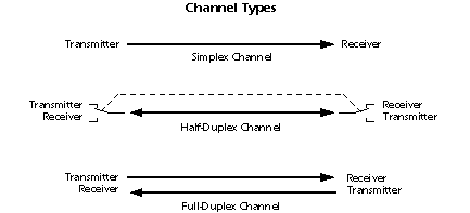
The message source is the transmitter, and the destination is the receiver. A channel whose direction of transmission is unchanging is referred to as a simplex channel. For example, a radio station is a simplex channel because it always transmits the signal to its listeners and never allows them to transmit back.
A half-duplex channel is a single physical channel in which the direction may be reversed. Messages may flow in two directions, but never at the same time, in a half-duplex system. In a telephone call, one party speaks while the other listens. After a pause, the other party speaks and the first party listens. Speaking simultaneously results in garbled sound that cannot be understood.
A full-duplex channel allows simultaneous message exchange in both directions. It really consists of two simplex channels, a forward channel and a reverse channel, linking the same points. The transmission rate of the reverse channel may be slower if it is used only for flow control of the forward channel.
Most digital messages are vastly longer than just a few bits. Because it is neither practical nor economic to transfer all bits of a long message simultaneously, the message is broken into smaller parts and transmitted sequentially. Bit-serial transmission conveys a message one bit at a time through a channel. Each bit represents a part of the message. The individual bits are then reassembled at the destination to compose the message. In general, one channel will pass only one bit at a time. Thus, bit-serial transmission is necessary in data communications if only a single channel is available. Bit-serial transmission is normally just called serial transmission and is the chosen communications method in many computer peripherals.
Byte-serial transmission conveys eight bits at a time through eight parallel channels. Although the raw transfer rate is eight times faster than in bit-serial transmission, eight channels are needed, and the cost may be as much as eight times higher to transmit the message. When distances are short, it may nonetheless be both feasible and economic to use parallel channels in return for high data rates. The popular Centronics printer interface is a case where byte-serial transmission is used. As another example, it is common practice to use a 16-bit-wide data bus to transfer data between a microprocessor and memory chips; this provides the equivalent of 16 parallel channels. On the other hand, when communicating with a timesharing system over a modem, only a single channel is available, and bit-serial transmission is required. This figure illustrates these ideas:
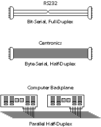
The baud rate refers to the signalling rate at which data is sent through a channel and is measured in electrical transitions per second. In the EIA232 serial interface standard, one signal transition, at most, occurs per bit, and the baud rate and bit rate are identical. In this case, a rate of 9600 baud corresponds to a transfer of 9,600 data bits per second with a bit period of 104 microseconds (1/9600 sec.). If two electrical transitions were required for each bit, as is the case in non-return-to-zero coding, then at a rate of 9600 baud, only 4800 bits per second could be conveyed. The channel efficiency is the number of bits of useful information passed through the channel per second. It does not include framing, formatting, and error detecting bits that may be added to the information bits before a message is transmitted, and will always be less than one.
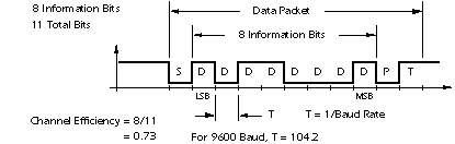
The data rate of a channel is often specified by its bit rate (often thought erroneously to be the same as baud rate). However, an equivalent measure channel capacity is bandwidth. In general, the maximum data rate a channel can support is directly proportional to the channel's bandwidth and inversely proportional to the channel's noise level.
A communications protocol is an agreed-upon convention that defines the order and meaning of bits in a serial transmission. It may also specify a procedure for exchanging messages. A protocol will define how many data bits compose a message unit, the framing and formatting bits, any error-detecting bits that may be added, and other information that governs control of the communications hardware. Channel efficiency is determined by the protocol design rather than by digital hardware considerations. Note that there is a tradeoff between channel efficiency and reliability - protocols that provide greater immunity to noise by adding error-detecting and -correcting codes must necessarily become less efficient.
Serialized data is not generally sent at a uniform rate through a channel. Instead, there is usually a burst of regularly spaced binary data bits followed by a pause, after which the data flow resumes. Packets of binary data are sent in this manner, possibly with variable-length pauses between packets, until the message has been fully transmitted. In order for the receiving end to know the proper moment to read individual binary bits from the channel, it must know exactly when a packet begins and how much time elapses between bits. When this timing information is known, the receiver is said to be synchronized with the transmitter, and accurate data transfer becomes possible. Failure to remain synchronized throughout a transmission will cause data to be corrupted or lost.
Two basic techniques are employed to ensure correct synchronization. In synchronous systems, separate channels are used to transmit data and timing information. The timing channel transmits clock pulses to the receiver. Upon receipt of a clock pulse, the receiver reads the data channel and latches the bit value found on the channel at that moment. The data channel is not read again until the next clock pulse arrives. Because the transmitter originates both the data and the timing pulses, the receiver will read the data channel only when told to do so by the transmitter (via the clock pulse), and synchronization is guaranteed.
Techniques exist to merge the timing signal with the data so that only a single channel is required. This is especially useful when synchronous transmissions are to be sent through a modem. Two methods in which a data signal is self-timed are nonreturn-to-zero and biphase Manchester coding. These both refer to methods for encoding a data stream into an electrical waveform for transmission.
In asynchronous systems, a separate timing channel is not used. The transmitter and receiver must be preset in advance to an agreed-upon baud rate. A very accurate local oscillator within the receiver will then generate an internal clock signal that is equal to the transmitter's within a fraction of a percent. For the most common serial protocol, data is sent in small packets of 10 or 11 bits, eight of which constitute message information. When the channel is idle, the signal voltage corresponds to a continuous logic '1'. A data packet always begins with a logic '0' (the start bit) to signal the receiver that a transmission is starting. The start bit triggers an internal timer in the receiver that generates the needed clock pulses. Following the start bit, eight bits of message data are sent bit by bit at the agreed upon baud rate. The packet is concluded with a parity bit and stop bit. One complete packet is illustrated below:
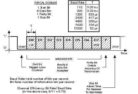
The packet length is short in asynchronous systems to minimize the risk that the local oscillators in the receiver and transmitter will drift apart. When high-quality crystal oscillators are used, synchronization can be guaranteed over an 11-bit period. Every time a new packet is sent, the start bit resets the synchronization, so the pause between packets can be arbitrarily long. Note that the EIA232 standard defines electrical, timing, and mechanical characteristics of a serial interface. However, it does not include the asynchronous serial protocol shown in the previous figure, or the ASCII alphabet described next.
Characters sent through a serial interface generally follow the ASCII (American Standard Code for Information Interchange) character standard:
This standard relates binary codes to printable characters and control codes. Fully 25 percent of the ASCII character set represents nonprintable control codes, such as carriage return (CR) and line feed (LF). Most modern character-oriented peripheral equipment abides by the ASCII standard, and thus may be used interchangeably with different computers.
Noise and momentary electrical disturbances may cause data to be changed as it passes through a communications channel. If the receiver fails to detect this, the received message will be incorrect, resulting in possibly serious consequences. As a first line of defense against data errors, they must be detected. If an error can be flagged, it might be possible to request that the faulty packet be resent, or to at least prevent the flawed data from being taken as correct. If sufficient redundant information is sent, one- or two-bit errors may be corrected by hardware within the receiver before the corrupted data ever reaches its destination.
A parity bit is added to a data packet for the purpose of error detection. In the even-parity convention, the value of the parity bit is chosen so that the total number of '1' digits in the combined data plus parity packet is an even number. Upon receipt of the packet, the parity needed for the data is recomputed by local hardware and compared to the parity bit received with the data. If any bit has changed state, the parity will not match, and an error will have been detected. In fact, if an odd number of bits (not just one) have been altered, the parity will not match. If an even number of bits have been reversed, the parity will match even though an error has occurred. However, a statistical analysis of data communication errors has shown that a single-bit error is much more probable than a multibit error in the presence of random noise. Thus, parity is a reliable method of error detection.
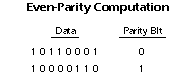
Another approach to error detection involves the computation of a checksum. In this case, the packets that constitute a message are added arithmetically. A checksum number is appended to the packet sequence so that the sum of data plus checksum is zero. When received, the packet sequence may be added, along with the checksum, by a local microprocessor. If the sum is nonzero, an error has occurred. As long as the sum is zero, it is highly unlikely (but not impossible) that any data has been corrupted during transmission.
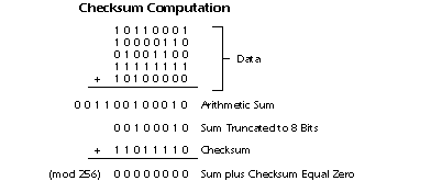
Errors may not only be detected, but also corrected if additional code is added to a packet sequence. If the error probability is high or if it is not possible to request retransmission, this may be worth doing. However, including error-correcting code in a transmission lowers channel efficiency, and results in a noticeable drop in channel throughput.
If a typical message were statistically analyzed, it would be found that certain characters are used much more frequently than others. By analyzing a message before it is transmitted, short binary codes may be assigned to frequently used characters and longer codes to rarely used characters. In doing so, it is possible to reduce the total number of characters sent without altering the information in the message. Appropriate decoding at the receiver will restore the message to its original form. This procedure, known as data compression, may result in a 50 percent or greater savings in the amount of data transmitted. Even though time is necessary to analyze the message before it is transmitted, the savings may be great enough so that the total time for compression, transmission, and decompression will still be lower than it would be when sending an uncompressed message.
Some kinds of data will compress much more than others. Data that represents images, for example, will usually compress significantly, perhaps by as much as 80 percent over its original size. Data representing a computer program, on the other hand, may be reduced only by 15 or 20 percent.
A compression method called Huffman coding is frequently used in data communications, and particularly in fax transmission. Clearly, most of the image data for a typical business letter represents white paper, and only about 5 percent of the surface represents black ink. It is possible to send a single code that, for example, represents a consecutive string of 1000 white pixels rather than a separate code for each white pixel. Consequently, data compression will significantly reduce the total message length for a faxed business letter. Were the letter made up of randomly distributed black ink covering 50 percent of the white paper surface, data compression would hold no advantages.
Privacy is a great concern in data communications. Faxed business letters can be intercepted at will through tapped phone lines or intercepted microwave transmissions without the knowledge of the sender or receiver. To increase the security of this and other data communications, including digitized telephone conversations, the binary codes representing data may be scrambled in such a way that unauthorized interception will produce an indecipherable sequence of characters. Authorized receive stations will be equipped with a decoder that enables the message to be restored. The process of scrambling, transmitting, and descrambling is known as encryption.
Custom integrated circuits have been designed to perform this task and are available at low cost. In some cases, they will be incorporated into the main circuitry of a data communications device and function without operator knowledge. In other cases, an external circuit is used so that the device, and its encrypting/decrypting technique, may be transported easily.
Normally, we think of communications science as dealing with the contemporaneous exchange of information between distant parties. However, many of the same techniques employed in data communications are also applied to data storage to ensure that the retrieval of information from a storage medium is accurate. We find, for example, that similar kinds of error-correcting codes used to protect digital telephone transmissions from noise are also used to guarantee correct readback of digital data from compact audio disks, CD-ROMs, and tape backup systems.
Data is typically grouped into packets that are either 8, 16, or 32 bits long, and passed between temporary holding units called registers. Data within a register is available in parallel because each bit exits the register on a separate conductor. To transfer data from one register to another, the output conductors of one register are switched onto a channel of parallel wires referred to as a bus. The input conductors of another register, which is also connected to the bus, capture the information:
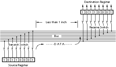
Following a data transaction, the content of the source register is reproduced in the destination register. It is important to note that after any digital data transfer, the source and destination registers are equal; the source register is not erased when the data is sent.
The transmit and receive switches shown above are electronic and operate in response to commands from a central control unit. It is possible that two or more destination registers will be switched on to receive data from a single source. However, only one source may transmit data onto the bus at any time. If multiple sources were to attempt transmission simultaneously, an electrical conflict would occur when bits of opposite value are driven onto a single bus conductor. Such a condition is referred to as a bus contention. Not only will a bus contention result in the loss of information, but it also may damage the electronic circuitry. As long as all registers in a system are linked to one central control unit, bus contentions should never occur if the circuit has been designed properly. Note that the data buses within a typical microprocessor are funda-mentally half-duplex channels.
When the source and destination registers are part of an integrated circuit (within a microprocessor chip, for example), they are extremely close (thousandths of an inch). Consequently, the bus signals are at very low power levels, may traverse a distance in very little time, and are not very susceptible to external noise and distortion. This is the ideal environment for digital communications. However, it is not yet possible to integrate all the necessary circuitry for a computer (i.e., CPU, memory, disk control, video and display drivers, etc.) on a single chip. When data is sent off-chip to another integrated circuit, the bus signals must be amplified and conductors extended out of the chip through external pins. Amplifiers may be added to the source register:
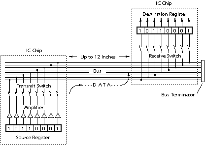
Bus signals that exit microprocessor chips and other VLSI circuitry are electrically capable of traversing about one foot of conductor on a printed circuit board, or less if many devices are connected to it. Special buffer circuits may be added to boost the bus signals sufficiently for transmission over several additional feet of conductor length, or for distribution to many other chips (such as memory chips).
Because of the very high switching rate and relatively low signal strength found on data, address, and other buses within a computer, direct extension of the buses beyond the confines of the main circuit board or plug-in boards would pose serious problems. First, long runs of electrical conductors, either on printed circuit boards or through cables, act like receiving antennas for electrical noise radiated by motors, switches, and electronic circuits:
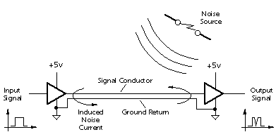
Such noise becomes progressively worse as the length increases, and may eventually impose an unacceptable error rate on the bus signals. Just a single bit error in transferring an instruction code from memory to a microprocessor chip may cause an invalid instruction to be introduced into the instruction stream, in turn causing the computer to totally cease operation.
A second problem involves the distortion of electrical signals as they pass through metallic conductors. Signals that start at the source as clean, rectangular pulses may be received as rounded pulses with ringing at the rising and falling edges:
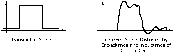
These effects are properties of transmission through metallic conductors, and become more pronounced as the conductor length increases. To compensate for distortion, signal power must be increased or the transmission rate decreased.
Special amplifier circuits are designed for transmitting direct (unmodulated) digital signals through cables. For the relatively short distances between components on a printed circuit board or along a computer backplane, the amplifiers are in simple IC chips that operate from standard +5v power. The normal output voltage from the amplifier for logic '1' is slightly higher than the minimum needed to pass the logic '1' threshold. Correspondingly for logic '0', it is slightly lower. The difference between the actual output voltage and the threshold value is referred to as the noise margin, and represents the amount of noise voltage that can be added to the signal without creating an error:
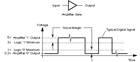
Computer peripherals such as a printer or scanner generally include mechanisms that cannot be situated within the computer itself. Our first thought might be just to extend the computer's internal buses with a cable of sufficient length to reach the peripheral. Doing so, however, would expose all bus transactions to external noise and distortion even though only a very small percentage of these transactions concern the distant peripheral to which the bus is connected.
If a peripheral can be located within 20 feet of the computer, however, relatively simple electronics may be added to make data transfer through a cable efficient and reliable. To accomplish this, a bus interface circuit is installed in the computer:
It consists of a holding register for peripheral data, timing and formatting circuitry for external data transmission, and signal amplifiers to boost the signal sufficiently for transmission through a cable. When communication with the peripheral is necessary, data is first deposited in the holding register by the microprocessor. This data will then be reformatted, sent with error-detecting codes, and transmitted at a relatively slow rate by digital hardware in the bus interface circuit. In addition, the signal power is greatly boosted before transmission through the cable. These steps ensure that the data will not be corrupted by noise or distortion during its passage through the cable. In addition, because only data destined for the peripheral is sent, the party-line transactions taking place on the computer's buses are not unnecessarily exposed to noise.
Data sent in this manner may be transmitted in byte-serial format if the cable has eight parallel channels (at least 10 conductors for half-duplex operation), or in bit-serial format if only a single channel is available.
When relatively long distances are involved in reaching a peripheral device, driver circuits must be inserted after the bus interface unit to compensate for the electrical effects of long cables:
This is the only change needed if a single peripheral is used. However, if many peripherals are connected, or if other computer stations are to be linked, a local area network (LAN) is required, and it becomes necessary to drastically change both the electrical drivers and the protocol to send messages through the cable. Because multiconductor cable is expensive, bit-serial transmission is almost always used when the distance exceeds 20 feet.
In either a simple extension cable or a LAN, a balanced electrical system is used for transmitting digital data through the channel. This type of system involves at least two wires per channel, neither of which is a ground. Note that a common ground return cannot be shared by multiple channels in the same cable as would be possible in an unbalanced system.
The basic idea behind a balanced circuit is that a digital signal is sent on two wires simultaneously, one wire expressing a positive voltage image of the signal and the other a negative voltage image. When both wires reach the destination, the signals are subtracted by a summing amplifier, producing a signal swing of twice the value found on either incoming line. If the cable is exposed to radiated electrical noise, a small voltage of the same polarity is added to both wires in the cable. When the signals are subtracted by the summing amplifier, the noise cancels and the signal emerges from the cable without noise:
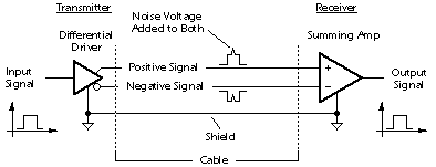
A great deal of technology has been developed for LAN systems to minimize the amount of cable required and maximize the throughput. The costs of a LAN have been concentrated in the electrical interface card that would be installed in PCs or peripherals to drive the cable, and in the communications software, not in the cable itself (whose cost has been minimized). Thus, the cost and complexity of a LAN are not particularly affected by the distance between stations.
Data communications through the telephone network can reach any point in the world. The volume of overseas fax transmissions is increasing constantly, and computer networks that link thousands of businesses, governments, and universities are pervasive. Transmissions over such distances are not generally accomplished with a direct-wire digital link, but rather with digitally-modulated analog carrier signals. This technique makes it possible to use existing analog telephone voice channels for digital data, although at considerably reduced data rates compared to a direct digital link.
Transmission of data from your personal computer to a timesharing service over phone lines requires that data signals be converted to audible tones by a modem. An audio sine wave carrier is used, and, depending on the baud rate and protocol, will encode data by varying the frequency, phase, or amplitude of the carrier. The receiver's modem accepts the modulated sine wave and extracts the digital data from it. Several modulation techniques typically used in encoding digital data for analog transmission are shown below:
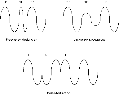
Similar techniques may be used in digital storage devices such as hard disk drives to encode data for storage using an analog medium.
====== MA THE ELECTRONIC ELBIT MATIC ======
The distance over which data moves within a computer may vary from a few thousandths of an inch, as is the case within a single IC chip, to as much as several feet along the backplane of the main circuit board. Over such small distances, digital data may be transmitted as direct, two-level electrical signals over simple copper conductors. Except for the fastest computers, circuit designers are not very concerned about the shape of the conductor or the analog characteristics of signal transmission.
Frequently, however, data must be sent beyond the local circuitry that constitutes a computer. In many cases, the distances involved may be enormous. Unfortunately, as the distance between the source of a message and its destination increases, accurate transmission becomes increasingly difficult. This results from the electrical distortion of signals traveling through long conductors, and from noise added to the signal as it propagates through a transmission medium. Although some precautions must be taken for data exchange within a computer, the biggest problems occur when data is transferred to devices outside the computer's circuitry. In this case, distortion and noise can become so severe that information is lost.
Data Communications concerns the transmission of digital messages to devices external to the message source. "External" devices are generally thought of as being independently powered circuitry that exists beyond the chassis of a computer or other digital message source. As a rule, the maximum permissible transmission rate of a message is directly proportional to signal power, and inversely proportional to channel noise. It is the aim of any communications system to provide the highest possible transmission rate at the lowest possible power and with the least possible noise.
Communications Channels
A communications channel is a pathway over which information can be conveyed. It may be defined by a physical wire that connects communicating devices, or by a radio, laser, or other radiated energy source that has no obvious physical presence. Information sent through a communications channel has a source from which the information originates, and a destination to which the information is delivered. Although information originates from a single source, there may be more than one destination, depending upon how many receive stations are linked to the channel and how much energy the transmitted signal possesses.
In a digital communications channel, the information is represented by individual data bits, which may be encapsulated into multibit message units. A byte, which consists of eight bits, is an example of a message unit that may be conveyed through a digital communications channel. A collection of bytes may itself be grouped into a frame or other higher-level message unit. Such multiple levels of encapsulation facilitate the handling of messages in a complex data communications network.
Any communications channel has a direction associated with it:
A half-duplex channel is a single physical channel in which the direction may be reversed. Messages may flow in two directions, but never at the same time, in a half-duplex system. In a telephone call, one party speaks while the other listens. After a pause, the other party speaks and the first party listens. Speaking simultaneously results in garbled sound that cannot be understood.
A full-duplex channel allows simultaneous message exchange in both directions. It really consists of two simplex channels, a forward channel and a reverse channel, linking the same points. The transmission rate of the reverse channel may be slower if it is used only for flow control of the forward channel.
Serial Communications
Most digital messages are vastly longer than just a few bits. Because it is neither practical nor economic to transfer all bits of a long message simultaneously, the message is broken into smaller parts and transmitted sequentially. Bit-serial transmission conveys a message one bit at a time through a channel. Each bit represents a part of the message. The individual bits are then reassembled at the destination to compose the message. In general, one channel will pass only one bit at a time. Thus, bit-serial transmission is necessary in data communications if only a single channel is available. Bit-serial transmission is normally just called serial transmission and is the chosen communications method in many computer peripherals.
Byte-serial transmission conveys eight bits at a time through eight parallel channels. Although the raw transfer rate is eight times faster than in bit-serial transmission, eight channels are needed, and the cost may be as much as eight times higher to transmit the message. When distances are short, it may nonetheless be both feasible and economic to use parallel channels in return for high data rates. The popular Centronics printer interface is a case where byte-serial transmission is used. As another example, it is common practice to use a 16-bit-wide data bus to transfer data between a microprocessor and memory chips; this provides the equivalent of 16 parallel channels. On the other hand, when communicating with a timesharing system over a modem, only a single channel is available, and bit-serial transmission is required. This figure illustrates these ideas:
The baud rate refers to the signalling rate at which data is sent through a channel and is measured in electrical transitions per second. In the EIA232 serial interface standard, one signal transition, at most, occurs per bit, and the baud rate and bit rate are identical. In this case, a rate of 9600 baud corresponds to a transfer of 9,600 data bits per second with a bit period of 104 microseconds (1/9600 sec.). If two electrical transitions were required for each bit, as is the case in non-return-to-zero coding, then at a rate of 9600 baud, only 4800 bits per second could be conveyed. The channel efficiency is the number of bits of useful information passed through the channel per second. It does not include framing, formatting, and error detecting bits that may be added to the information bits before a message is transmitted, and will always be less than one.
The data rate of a channel is often specified by its bit rate (often thought erroneously to be the same as baud rate). However, an equivalent measure channel capacity is bandwidth. In general, the maximum data rate a channel can support is directly proportional to the channel's bandwidth and inversely proportional to the channel's noise level.
A communications protocol is an agreed-upon convention that defines the order and meaning of bits in a serial transmission. It may also specify a procedure for exchanging messages. A protocol will define how many data bits compose a message unit, the framing and formatting bits, any error-detecting bits that may be added, and other information that governs control of the communications hardware. Channel efficiency is determined by the protocol design rather than by digital hardware considerations. Note that there is a tradeoff between channel efficiency and reliability - protocols that provide greater immunity to noise by adding error-detecting and -correcting codes must necessarily become less efficient.
Asynchronous vs. Synchronous Transmission
Serialized data is not generally sent at a uniform rate through a channel. Instead, there is usually a burst of regularly spaced binary data bits followed by a pause, after which the data flow resumes. Packets of binary data are sent in this manner, possibly with variable-length pauses between packets, until the message has been fully transmitted. In order for the receiving end to know the proper moment to read individual binary bits from the channel, it must know exactly when a packet begins and how much time elapses between bits. When this timing information is known, the receiver is said to be synchronized with the transmitter, and accurate data transfer becomes possible. Failure to remain synchronized throughout a transmission will cause data to be corrupted or lost.
Two basic techniques are employed to ensure correct synchronization. In synchronous systems, separate channels are used to transmit data and timing information. The timing channel transmits clock pulses to the receiver. Upon receipt of a clock pulse, the receiver reads the data channel and latches the bit value found on the channel at that moment. The data channel is not read again until the next clock pulse arrives. Because the transmitter originates both the data and the timing pulses, the receiver will read the data channel only when told to do so by the transmitter (via the clock pulse), and synchronization is guaranteed.
Techniques exist to merge the timing signal with the data so that only a single channel is required. This is especially useful when synchronous transmissions are to be sent through a modem. Two methods in which a data signal is self-timed are nonreturn-to-zero and biphase Manchester coding. These both refer to methods for encoding a data stream into an electrical waveform for transmission.
In asynchronous systems, a separate timing channel is not used. The transmitter and receiver must be preset in advance to an agreed-upon baud rate. A very accurate local oscillator within the receiver will then generate an internal clock signal that is equal to the transmitter's within a fraction of a percent. For the most common serial protocol, data is sent in small packets of 10 or 11 bits, eight of which constitute message information. When the channel is idle, the signal voltage corresponds to a continuous logic '1'. A data packet always begins with a logic '0' (the start bit) to signal the receiver that a transmission is starting. The start bit triggers an internal timer in the receiver that generates the needed clock pulses. Following the start bit, eight bits of message data are sent bit by bit at the agreed upon baud rate. The packet is concluded with a parity bit and stop bit. One complete packet is illustrated below:
The packet length is short in asynchronous systems to minimize the risk that the local oscillators in the receiver and transmitter will drift apart. When high-quality crystal oscillators are used, synchronization can be guaranteed over an 11-bit period. Every time a new packet is sent, the start bit resets the synchronization, so the pause between packets can be arbitrarily long. Note that the EIA232 standard defines electrical, timing, and mechanical characteristics of a serial interface. However, it does not include the asynchronous serial protocol shown in the previous figure, or the ASCII alphabet described next.
The ASCII Character Set
Characters sent through a serial interface generally follow the ASCII (American Standard Code for Information Interchange) character standard:
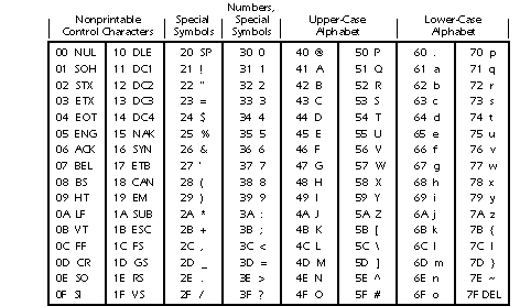
This standard relates binary codes to printable characters and control codes. Fully 25 percent of the ASCII character set represents nonprintable control codes, such as carriage return (CR) and line feed (LF). Most modern character-oriented peripheral equipment abides by the ASCII standard, and thus may be used interchangeably with different computers.
Parity and Checksums
Noise and momentary electrical disturbances may cause data to be changed as it passes through a communications channel. If the receiver fails to detect this, the received message will be incorrect, resulting in possibly serious consequences. As a first line of defense against data errors, they must be detected. If an error can be flagged, it might be possible to request that the faulty packet be resent, or to at least prevent the flawed data from being taken as correct. If sufficient redundant information is sent, one- or two-bit errors may be corrected by hardware within the receiver before the corrupted data ever reaches its destination.
A parity bit is added to a data packet for the purpose of error detection. In the even-parity convention, the value of the parity bit is chosen so that the total number of '1' digits in the combined data plus parity packet is an even number. Upon receipt of the packet, the parity needed for the data is recomputed by local hardware and compared to the parity bit received with the data. If any bit has changed state, the parity will not match, and an error will have been detected. In fact, if an odd number of bits (not just one) have been altered, the parity will not match. If an even number of bits have been reversed, the parity will match even though an error has occurred. However, a statistical analysis of data communication errors has shown that a single-bit error is much more probable than a multibit error in the presence of random noise. Thus, parity is a reliable method of error detection.
Another approach to error detection involves the computation of a checksum. In this case, the packets that constitute a message are added arithmetically. A checksum number is appended to the packet sequence so that the sum of data plus checksum is zero. When received, the packet sequence may be added, along with the checksum, by a local microprocessor. If the sum is nonzero, an error has occurred. As long as the sum is zero, it is highly unlikely (but not impossible) that any data has been corrupted during transmission.
Errors may not only be detected, but also corrected if additional code is added to a packet sequence. If the error probability is high or if it is not possible to request retransmission, this may be worth doing. However, including error-correcting code in a transmission lowers channel efficiency, and results in a noticeable drop in channel throughput.
Data Compression
If a typical message were statistically analyzed, it would be found that certain characters are used much more frequently than others. By analyzing a message before it is transmitted, short binary codes may be assigned to frequently used characters and longer codes to rarely used characters. In doing so, it is possible to reduce the total number of characters sent without altering the information in the message. Appropriate decoding at the receiver will restore the message to its original form. This procedure, known as data compression, may result in a 50 percent or greater savings in the amount of data transmitted. Even though time is necessary to analyze the message before it is transmitted, the savings may be great enough so that the total time for compression, transmission, and decompression will still be lower than it would be when sending an uncompressed message.
Some kinds of data will compress much more than others. Data that represents images, for example, will usually compress significantly, perhaps by as much as 80 percent over its original size. Data representing a computer program, on the other hand, may be reduced only by 15 or 20 percent.
A compression method called Huffman coding is frequently used in data communications, and particularly in fax transmission. Clearly, most of the image data for a typical business letter represents white paper, and only about 5 percent of the surface represents black ink. It is possible to send a single code that, for example, represents a consecutive string of 1000 white pixels rather than a separate code for each white pixel. Consequently, data compression will significantly reduce the total message length for a faxed business letter. Were the letter made up of randomly distributed black ink covering 50 percent of the white paper surface, data compression would hold no advantages.
Data Encryption
Privacy is a great concern in data communications. Faxed business letters can be intercepted at will through tapped phone lines or intercepted microwave transmissions without the knowledge of the sender or receiver. To increase the security of this and other data communications, including digitized telephone conversations, the binary codes representing data may be scrambled in such a way that unauthorized interception will produce an indecipherable sequence of characters. Authorized receive stations will be equipped with a decoder that enables the message to be restored. The process of scrambling, transmitting, and descrambling is known as encryption.
Custom integrated circuits have been designed to perform this task and are available at low cost. In some cases, they will be incorporated into the main circuitry of a data communications device and function without operator knowledge. In other cases, an external circuit is used so that the device, and its encrypting/decrypting technique, may be transported easily.
Data Storage Technology
Normally, we think of communications science as dealing with the contemporaneous exchange of information between distant parties. However, many of the same techniques employed in data communications are also applied to data storage to ensure that the retrieval of information from a storage medium is accurate. We find, for example, that similar kinds of error-correcting codes used to protect digital telephone transmissions from noise are also used to guarantee correct readback of digital data from compact audio disks, CD-ROMs, and tape backup systems.
Data Transfer in Digital Circuits
Data is typically grouped into packets that are either 8, 16, or 32 bits long, and passed between temporary holding units called registers. Data within a register is available in parallel because each bit exits the register on a separate conductor. To transfer data from one register to another, the output conductors of one register are switched onto a channel of parallel wires referred to as a bus. The input conductors of another register, which is also connected to the bus, capture the information:
Following a data transaction, the content of the source register is reproduced in the destination register. It is important to note that after any digital data transfer, the source and destination registers are equal; the source register is not erased when the data is sent.
The transmit and receive switches shown above are electronic and operate in response to commands from a central control unit. It is possible that two or more destination registers will be switched on to receive data from a single source. However, only one source may transmit data onto the bus at any time. If multiple sources were to attempt transmission simultaneously, an electrical conflict would occur when bits of opposite value are driven onto a single bus conductor. Such a condition is referred to as a bus contention. Not only will a bus contention result in the loss of information, but it also may damage the electronic circuitry. As long as all registers in a system are linked to one central control unit, bus contentions should never occur if the circuit has been designed properly. Note that the data buses within a typical microprocessor are funda-mentally half-duplex channels.
Transmission over Short Distances (< 2 feet)
When the source and destination registers are part of an integrated circuit (within a microprocessor chip, for example), they are extremely close (thousandths of an inch). Consequently, the bus signals are at very low power levels, may traverse a distance in very little time, and are not very susceptible to external noise and distortion. This is the ideal environment for digital communications. However, it is not yet possible to integrate all the necessary circuitry for a computer (i.e., CPU, memory, disk control, video and display drivers, etc.) on a single chip. When data is sent off-chip to another integrated circuit, the bus signals must be amplified and conductors extended out of the chip through external pins. Amplifiers may be added to the source register:
Bus signals that exit microprocessor chips and other VLSI circuitry are electrically capable of traversing about one foot of conductor on a printed circuit board, or less if many devices are connected to it. Special buffer circuits may be added to boost the bus signals sufficiently for transmission over several additional feet of conductor length, or for distribution to many other chips (such as memory chips).
Noise and Electrical Distortion
Because of the very high switching rate and relatively low signal strength found on data, address, and other buses within a computer, direct extension of the buses beyond the confines of the main circuit board or plug-in boards would pose serious problems. First, long runs of electrical conductors, either on printed circuit boards or through cables, act like receiving antennas for electrical noise radiated by motors, switches, and electronic circuits:
Such noise becomes progressively worse as the length increases, and may eventually impose an unacceptable error rate on the bus signals. Just a single bit error in transferring an instruction code from memory to a microprocessor chip may cause an invalid instruction to be introduced into the instruction stream, in turn causing the computer to totally cease operation.
A second problem involves the distortion of electrical signals as they pass through metallic conductors. Signals that start at the source as clean, rectangular pulses may be received as rounded pulses with ringing at the rising and falling edges:
These effects are properties of transmission through metallic conductors, and become more pronounced as the conductor length increases. To compensate for distortion, signal power must be increased or the transmission rate decreased.
Special amplifier circuits are designed for transmitting direct (unmodulated) digital signals through cables. For the relatively short distances between components on a printed circuit board or along a computer backplane, the amplifiers are in simple IC chips that operate from standard +5v power. The normal output voltage from the amplifier for logic '1' is slightly higher than the minimum needed to pass the logic '1' threshold. Correspondingly for logic '0', it is slightly lower. The difference between the actual output voltage and the threshold value is referred to as the noise margin, and represents the amount of noise voltage that can be added to the signal without creating an error:
Transmission over Medium Distances (< 20 feet)
Computer peripherals such as a printer or scanner generally include mechanisms that cannot be situated within the computer itself. Our first thought might be just to extend the computer's internal buses with a cable of sufficient length to reach the peripheral. Doing so, however, would expose all bus transactions to external noise and distortion even though only a very small percentage of these transactions concern the distant peripheral to which the bus is connected.
If a peripheral can be located within 20 feet of the computer, however, relatively simple electronics may be added to make data transfer through a cable efficient and reliable. To accomplish this, a bus interface circuit is installed in the computer:
It consists of a holding register for peripheral data, timing and formatting circuitry for external data transmission, and signal amplifiers to boost the signal sufficiently for transmission through a cable. When communication with the peripheral is necessary, data is first deposited in the holding register by the microprocessor. This data will then be reformatted, sent with error-detecting codes, and transmitted at a relatively slow rate by digital hardware in the bus interface circuit. In addition, the signal power is greatly boosted before transmission through the cable. These steps ensure that the data will not be corrupted by noise or distortion during its passage through the cable. In addition, because only data destined for the peripheral is sent, the party-line transactions taking place on the computer's buses are not unnecessarily exposed to noise.
Data sent in this manner may be transmitted in byte-serial format if the cable has eight parallel channels (at least 10 conductors for half-duplex operation), or in bit-serial format if only a single channel is available.
Transmission over Long Distances (< 4000 feet)
When relatively long distances are involved in reaching a peripheral device, driver circuits must be inserted after the bus interface unit to compensate for the electrical effects of long cables:
This is the only change needed if a single peripheral is used. However, if many peripherals are connected, or if other computer stations are to be linked, a local area network (LAN) is required, and it becomes necessary to drastically change both the electrical drivers and the protocol to send messages through the cable. Because multiconductor cable is expensive, bit-serial transmission is almost always used when the distance exceeds 20 feet.
In either a simple extension cable or a LAN, a balanced electrical system is used for transmitting digital data through the channel. This type of system involves at least two wires per channel, neither of which is a ground. Note that a common ground return cannot be shared by multiple channels in the same cable as would be possible in an unbalanced system.
The basic idea behind a balanced circuit is that a digital signal is sent on two wires simultaneously, one wire expressing a positive voltage image of the signal and the other a negative voltage image. When both wires reach the destination, the signals are subtracted by a summing amplifier, producing a signal swing of twice the value found on either incoming line. If the cable is exposed to radiated electrical noise, a small voltage of the same polarity is added to both wires in the cable. When the signals are subtracted by the summing amplifier, the noise cancels and the signal emerges from the cable without noise:
A great deal of technology has been developed for LAN systems to minimize the amount of cable required and maximize the throughput. The costs of a LAN have been concentrated in the electrical interface card that would be installed in PCs or peripherals to drive the cable, and in the communications software, not in the cable itself (whose cost has been minimized). Thus, the cost and complexity of a LAN are not particularly affected by the distance between stations.
Transmission over Very Long Distances (greater than 4000 feet)
Data communications through the telephone network can reach any point in the world. The volume of overseas fax transmissions is increasing constantly, and computer networks that link thousands of businesses, governments, and universities are pervasive. Transmissions over such distances are not generally accomplished with a direct-wire digital link, but rather with digitally-modulated analog carrier signals. This technique makes it possible to use existing analog telephone voice channels for digital data, although at considerably reduced data rates compared to a direct digital link.
Transmission of data from your personal computer to a timesharing service over phone lines requires that data signals be converted to audible tones by a modem. An audio sine wave carrier is used, and, depending on the baud rate and protocol, will encode data by varying the frequency, phase, or amplitude of the carrier. The receiver's modem accepts the modulated sine wave and extracts the digital data from it. Several modulation techniques typically used in encoding digital data for analog transmission are shown below:
Similar techniques may be used in digital storage devices such as hard disk drives to encode data for storage using an analog medium.
====== MA THE ELECTRONIC ELBIT MATIC ======
Tidak ada komentar:
Posting Komentar