active electronics and modern electronics function for the spacecraft and problems of reliability of electronic component AMNIMARJESLOW GOVERNMENT 91220017 LOR EL MODERN ELECTRONIC 02096010014 EL OPERATION AGING LJBUSAF XWAM ! XAM $$
XXX . V Spacecraft Information
Spacecraft Information
Image: NASA/JPL/Caltech
The core of the Juno Spacecraft is 3.5 meters tall and 3.5 meters in diameter. It is hexagonal in shape and features a two-deck structure. The vehicle utilizes composite panel and clip construction for decks, central cylinder and gusset panels. Juno has a liftoff mass of 3,625 Kilograms and is equipped with a variety of subsystems. Juno is a spin-stabilized spacecraft and does not use reaction wheels to maintain its attitude. Spin rates vary from one to five rpm during the different phases of the mission.
Propulsion System
Juno’s Electronics Vault – Photo: NASA/JPL
Juno utilizes a weight-saving and redundant approach to spacecraft propulsion with a bi-propellant main propulsion system and a monopropellant Reaction Control System. The main propulsion system uses Hydrazine as fuel and Nitrogen Tetroxide as oxidizer.
The propellant tanks are spherical in shape, surrounded by multilayer insulation and heaters that are activated several weeks before the burns occur to warm the propellants up to nominal temperatures, also ensuring that the transfer lines and tanks do not freeze in the space environment.
Juno is equipped with a single Leros 1b main engine. Leros 1b provides 645 Newtons of thrust and a specific impulse of 318sec. The engine is a coated Columbium Engine. It is fixed to the vehicle and can not be gimbaled for vehicle control. The main engine was manufactured by AMPAC-ISP in Westcott, UK.
A micrometeoroid and debris shield protects the engine when it is not in use. It is removed several days before a burn and is placed back in position after the maneuvers to protect the engine bell. The main propulsion system is only used for the Deep Space Maneuvers, the Jupiter Orbit Insertion Burn, the Period Reduction Maneuver and major Trajectory Correction Maneuvers.
To control is orientation in space and make small trajectory corrections, Juno is outfitted with a total of 12 reaction control system thrusters. The RCS uses Hydrazine for catalytic propulsion. The thrusters are installed on four engine modules and allow three-axis vehicle control. Three engines, one axial and two lateral, are installed on a single module. Two modules are on the forward deck and one on the aft deck.The REM towers are capable of providing medium delta-V and are sufficient for the Deorbit Burn of 75m/s.
A look at Juno’s business end – Leros 1b – Photo: NASA/JPL
Data System
RAD750 Card – Image: BAE Systems
Juno features a data handling system that is based on the RAD750 flight processor with 256 megabytes of flash memory and 128 megabytes of DRAM local memory. RAD750 is a flight processor designed to operate in the strongest radiation environments. It has substantial flight heritage and has already been proving itself on different mission such as NASA’s Mars Science Laboratory. Compared to most computers on Earth, Juno’s processor only features a fraction of their capabilities. But for space applications, electronics have to be able to endure the space radiation environment and provide stability. RAD750 is a single-card computer that was manufactured by BAE Systems in Manassas, Va. The processor can endure radiation doses that are a million times more extreme than what is considered fatal to humans.
Also, RAD750 will not suffer more than one event requiring interventions from Earth over a 15-year period. “The RAD750 card is designed to accommodate all those single event effects and survive them. The ultimate goal is one upset is allowed in 15 years. An upset means an intervention from Earth — one ‘blue screen of death’ in 15 years. We typically have contracts that (specify) that,” said Vic Scuderi BAE Business Manager. The RAD750 processors operate at up to 200 megahertz. With RAD750, Juno can support up to 100Mbps of total instrument throughput which is more than sufficient for the payload suite.
Electronics Vault
Photo: NASA/JPL Vault Installation – Photo: NASA
The heart of the Juno Spacecraft is the vehicle’s electronics vault that holds most of the vehicle’s electronics and protects them from the harsh environment Juno has to endure during its Cruise in deep space and especially when flying through Jupiter’s intense radiation belts.
The radiation vault is made of titanium metal with a thickness of one centimeter. The vault weighs 180 Kilograms and limits the radiation exposure of the mission to 25,000 Krad which can be tolerated by the vehicle’s electronics that are qualified for 50,000 Krad to account for any miscalculations of the radiation environment or vault design.
Juno’s top deck is planned to receive a radiation dose of 11 Mrad showing that the vault has a significant shielding effect.
The electronics vault had to withstand extensive thermal testing for the hot case (being near to Earth and the Sun) and the cold case (5.4 Astronomical Units from the Sun when being in Jupiter Orbit).
The vault has design features such as louvers to meet all thermal power requirements. The vault encloses Juno’s command and data handling box, power and data distribution unit and about 20 other electronic assemblies related to vehicle control and instrument operation.
.
Vault Design
Credit: NASA/JPL/Caltech
Power System
One of Juno’s three massive Solar Arrays – Photo: NASA/JPL
The power generation system of Juno consists of three solar array wings that are placed symmetrically around the spacecraft bus. At Jupiter, Juno receives about 25 times less Sunlight than we do on Earth. It is the first solar array-powered spacecraft to go this deep into space. Juno benefits from advances in solar cell design with modern cells that are 50 percent more efficient and radiation-tolerant than silicon cells available for space missions 20 years ago. Juno’s three solar arrays are 2.9 meters wide and 8.9 meters long, and consist of 11 individual solar panels – one arrays features the Magnetometer Boom instead of an eleventh solar panel. One of the three arrays is only 2.091 meters wide due to launch vehicle limitations.
With solar arrays deployed, Juno’s span is about 20 meters. Juno has a low, medium and high string of solar arrays that are activated as the vehicle increases its distance to the sun. Juno can tolerate solar cell failures which are expected when going through Jupiter’s radiation belts and failures have been calculated so that the power system has a fairly large margin.
Photo: NASA Kennedy
On average, the solar arrays produce about 460 to 490 watts of power when the vehicle arrives at Jupiter. End of mission power is planned to be 420 watts. The individual solar arrays can be articulated by a small amount in flight to control the vehicle’s center of gravity which is important to vehicle control and stability. When making engine burns, Juno consumes fuel which changes the spacecraft’s mass properties which are balanced out by adjusting the solar array position. Two 55 amp/hour lithium-ion batteries are used to store electrical power that is used when the spacecraft is in eclipse or its solar arrays are off-sun. For the duration of its mission, except for 10 minutes of eclipse during the Earth Flyby, Juno will be in daylight. The electrical power subsystem manages the vehicle’s power bus and distribution to payloads and instruments. A central power distribution and drive unit monitors the power that is generated by the solar arrays, distributes it to instruments, heaters and experiment sensors as well as batteries that are charged when excess power is available.
Thermal Control System
Image: NASA/JPL/Caltech
Due to its mission design, being in daylight most of the time, Juno is not facing the sudden temperature changes Low-Earth Orbiting satellites are experiencing when passing from day into night, but Juno is venturing out into deep space where warming sun radiation is limited. The electronics vault of the vehicle is insulated and has heaters and louvers to keep the electronics of the vehicle in a stable environment that meets the requirements of all components inside the vault. The propulsion system also features passive and active thermal control systems.
When being close to the Sun, Juno has to be protected from overheating. That is accomplished by pointing the High-Gain Antenna at the Sun. The large HGA covers almost the entire spacecraft bus so that the electronics vault and deck instruments are protected. Science instruments mounted on the outside of the vault have individual thermal requirements that are met by different insulations and heater assemblies.
Communications System
Juno’s High Gain Antenna Image: NASA/JPL/Caltech
Juno’s Communication System works as both, a science instrument and communication subsystem. The High Gain Antenna of the spacecraft supports X-Band communications with Earth for command uplink and science data & telemetry downlink. The subsystem also provides for dual-band (X- and Ka-band) Doppler tracking for gravity science at Jupiter.
Communications with Juno are accomplished by NASA’s Deep Space Network Stations. Juno also has low and medium gain communications system to provide continuous communications, even when the HGA is not pointing towards Earth which is the case when being close to the sun and during maneuvers. Juno has a fore medium gain antenna and a fore low gain antenna as well as an aft low gain antenna and a toroid LGA. Via its low gain antennas, Juno sends Tone signals which are 10-second, extremely low bandwidth data signals.
MFSK tones, or semaphores, are basic vehicle status messages. There is a library of 256 tones that includes such for the completion of major mission events. For successful completion of an event, one positive tone is reserved and when an operation is not completed, the negative version is sent.
On Earth, these tones can be translated into vehicle statuses that enable engineers to follow the vehicle’s progress without a direct telemetry link. Tones for Juno are available throughout Cruise, however is is not expected that those will be used often. During Jupiter Orbit insertion, tones are the only available communications opportunity since the HGA will not be pointing at Earth at that point.
Jason-3 Spacecraft & Instruments
Image: NOAA/NASA JPL
Jason-3 is an Ocean Altimetry Satellite in a U.S.-European satellite program to measure the height of the ocean surface.
The major objective of the Jason-3 mission is to extend the timeline of ocean surface topography measurements that were started by the Topex/Poseidon satellite in 1992 and continued through Jason-1 launching in 2001 and OSTM/Jason-2 that has been in operation since 2008. The ocean altimetry measurements are of vital importance when following the global circulation patterns, sea level changes and climate implications in a constantly warming world.
The primary instrument on the Jason-3 mission is a radar altimeter that can measure variations in sea level over the global oceans with a very high accuracy of 3.3 centimeters.
Photo: CNES/Thales Alenia Image: NOAA/NASA JPL
Long-term and continual data of changes in the oceans is essential for both, operational applications and scientific research. Operational use of ocean altimetry data can in the forecasting of hurricanes and severe weather, tracking weather patterns as they traverse the oceans, forecasting surface waves for offshore operators, tide forecasting and tracking of currents to aide commercial shipping and shipping routes, and forecasting of weather phenomena such as El Niño and La Niña. The scientific benefits of a long-term measurement of ocean topography provides insights into climate change processes.
The Jason-3 project was approved in 2010 to ensure a continuation of measurements made by Jason-2 and its predecessors. Agencies involved in the mission are first and foremost NOAA on the U.S. side and EUMETSAT representing the European member states.
NOAA and EUMETSAT are the lead agencies of the mission, involved with the operation of the satellites, processing the instrument data, distributing data products and archiving data. The French Space Agency CNES is providing support on the technical level and acts as a systems coordinator. The technical support provided by CNES includes making available the Proteus satellite bus used by Jason-3. NASA is in charge of supporting science team activities, delivering instruments and procuring the launch services for the mission.
The Jason-3 mission has the primary objective of continuing the ocean topography measurements started in 1992, but it also facilitates a shift from a separation between spacecraft dedicated purely to scientific observations and operational applications to a combination of the two in a single spacecraft. Moving satellite altimetry into routine operations such as Numerical Weather Prediction will require a tight cooperation and coordination by the international and multi-agency managers and data users. The change to a more operational than science-driven mission is also evident in NASA and CNES taking a back seat and leaving the conduct of mission to the operational agencies NOAA and EUMETSAT. Jason-3 is also part of a data exchange program between EUMETSAT and the Chinese National Satellite Ocean Application Service.
Image: CNES
The Jason-3 mission and its spacecraft design follows very closely the development methodology and overall architecture of the Jason-2 mission, taking into account updates of hardware due to obsolescence, unavailability or modernization of systems. The Jason-3 spacecraft, like its predecessor, uses the Proteus satellite bus of CNES and Thales Alenia Space coupled with a payload module. The satellite payload consists of the same core instruments as Jason-2 – a Poseidon-class radar altimeter operating at the Ku/C-Band frequencies for the primary ranging measurement, a nadir-looking microwave radiometer operating in three frequency bands, an orbit determination package using GPS and the DORIS payload, and a laser retroreflector. Two additional instruments, radiation dosimeters from CNES and Japan, are also part of the Jason-3 satellite payload.
The Proteus satellite bus provided by Thales Alenia is designed for Low Earth Orbit Missions with light-payloads between 300 and 1,000 Kilograms. The satellite bus consists of a cubic platform hosting all required subsystems, measuring 1 meter per side.
Photo: Thales Alenia/CNES
Overall, the Proteus platform for Jason-3 has a dry mass of around 250 Kilograms and interfaces with a payload module of 255 Kilograms. Contained within a central spherical tank are 28 Kilograms of hydrazine, creating a total launch mass of the Jason-3 satellite of 525 Kilograms. The spacecraft is 3.8 by 10 by 2 meters in size when fully deployed in orbit.
The Proteus satellite platform consists of an aluminum chassis to which honeycomb panels are mounted to provide attachment points for the various satellite subsystems. The satellite platform allows a payload assembly to be integrated in a modular fashion using four bolt interfaces. Thermal control relies on passive radiators with an area of 1.9m² along with a heater system to maintain components at their critical survival temperatures.
The satellite hosts two deployable solar arrays, each with four 1.5 by 0.8-meter panels covered with silicon solar cells to deliver a total power of 580 Watts. Each solar arrays has its own Solar Array Drive Mechanism to be able to track the sun and maximize the generation of electrical power. A Power Conditioning Unit receives power from the solar arrays and generates the satellite’s unregulated power bus at 23 to 37 Volts. Within the Power Conditioning Unit is a Digital Series Regulator that controls the state of charge of a 78 Amp-hour Li-Ion battery. Two identical power interfaces are run from the PCE to the Data Handling Unit where the power distribution function is centralized. A series of fuses and relays ensure bus protection inside the DHU and double isolation circuits upstream from the fuses provide further protection.
Star Tracker Assembly – Image: Thales Alenia/Space
The Attitude Determination and Control System of the satellite is in charge of precisely calculating the satellite’s three axis orientation in space and using a series of actuators to orient the satellite to its nominal attitude, for Jason-3 a nadir Earth-pointed orientation. Attitude Determination uses a gyro-stellar concept – using three accurate two-axis gyrometers during the stabilization of the satellite, that is reducing body rates to a point where a pair of Star Trackers can begin to acquire attitude frames. The Star Trackers, installed on the Payload Module, use optical sensors to collect imagery of the star-filled sky that are then compared to known star constellations by an onboard algorithm for an accurate determination of the satellite’s orientation. Also part of the Attitude Determination System are eight Coarse Sun Sensors and two three-axis magnetometers which come into play during satellite safe modes and operation of the magnetic torquers.
The Jason-3 satellite uses reaction wheels as its primary attitude actuation mechanism. The reaction wheel assembly is a rotating inertial mass that is driven by a brushless DC motor that spins the wheel. When accelerating the wheel, the satellite body to which the wheels are directly attached will rotate to the opposite direction as a result of the introduced counter torque.
Image: Thales Alenia/CNES
Because the reaction wheels have to be de-spun at regular intervals, the spacecraft requires a secondary mechanism capable of imparting controlled body rates on the satellite. Three Magnetic Torque Rods with redundant coils are used to create angular momentum by running a current through coils in the presence of Earth’s magnetic field. The torquers are regulated by computers that control the current that is passing through the coils in order to control the force generated on each axis. The magnetic torquers are used during momentum dumps and for attitude control in spacecraft safe mode. Actuation of the torquers is commanded based on readings from a three-axis magnetometer.
Overall, the Proteus satellite platform has a pointing accuracy exceeding 0.05 degrees.
The Data Handling Unit builds the brain of the satellite, hosting the onboard computer that runs the flight software to control all platform functions and handle data coming from the satellite payload. It is also responsible for failure detection and recovery, power distribution and command execution across the spacecraft. The main processor within the DHU is a MA 31750 and all interfaces between the DHU and the satellite payload use a 1553 link for commanding. Internal data speeds of up to 10Mbit/s can be supported by the satellite platform. All units within the DHU, including the main processor, are redundant. The satellite offers a mass memory of 2 Gbit to store payload data prior to downlink.
Image: Thales Alenia
The Jason-3 satellite carries a total propellant load of 28 Kilograms of Hydrazine monopropellant, pressurized with Nitrogen prior to launch and operated in a blow-down mode, starting out at an initial propellant pressure of 22 bar. The propellant tank feeds a single bank of 1-Newton thrusters, each with its own set of valves. To generate thrust, the system makes use of the catalytic decomposition of Hydrazine over a heated metallic catalyst bed. All four thrusters are installed on the +X face of the satellite to be able to come to use in orbit adjustment maneuvers. The overall delta-v budget of the Jason-3 mission is slightly less than 120 meters per second.
The Communications System of the satellite employs a redundant set of S-Band transceivers interfacing with a pair of feedhorns with cross strapping between the antennas and transceivers as well as the Central Processing Module within the DHU. The S-Band system uses QPSK modulation and reaches a downlink data rate of 838 kbit/s and 4kbit/s for uplink.
Jason-3 Instruments
Image: CNES
The Jason-3 mission’s primary instrument is the Poseidon-3B altimeter that provides the critical data continuity with the previous Jason missions while also improving measurement accuracy and instrument operation. Furthermore, the satellite hosts a passive microwave radiometer, known as Advanced Microwave Radiometer 2. The Precise Orbit Determination System, a laser retroreflector and a GPS payload are used to accurately determine the satellite’s location in orbit for proper geo-tagging of the collected data sets. Two passenger instruments hosted on the Jason-3 satellite are the Joint Radiation Experiment and the Light Particle Telescope.
The primary payload of the Jason-3 satellite combines an active and a passive instrument. The active radar pulses radio signals to the ground and records the radar echo which can yield information on Ocean typography while a passive microwave radiometer only records the ambient microwave emissions at the given wavelength range to deliver correction data accounting for atmospheric effects.
Image: NOAA/NESDIS/STAR
Poseidon-3B
Image: Thales Alenia/CNES
Image: Thales Alenia/CNES
Poseidon-3B, the primary instrument of the Jason-3 satellite, is a radar altimeter that precisely measures altitude above the terrain presently beneath the satellite by bouncing a radio wave off the ground and measuring how long it takes to return to the satellite. Recording the signal waveforms that return from the ocean surface allows the topography of the sea surface to be mapped and the ocean surface current velocity, wave height and wind speeds to be calculated.
The Poseidon-3B instrument has a mass of 70 Kilograms and requires 78 Watts of Power, hosting a radar antenna 1.20 meters in diameter. It operates at two transmission frequencies one in C-Band at 5.3 GHz and one in Ku-Band at 13.575 GHz, both using a bandwidth of 320 MHz. Each radar pulse is 105.6 microseconds in duration and Poseidon-3 employs an interlaced pulse pattern consisting of three Ku pulses followed by one C-Band pulse followed by three Ku pulses and so on, achieving a Pulse Repetition Frequency of 2060Hz.
Using a dual-frequency radar system allows processing to determine the atmospheric electron content which can affect the signal return time and in turn decrease measurement accuracy. The delay caused by free electrons is directly dependent on the radar frequency and using two different frequencies allows an easy calculation of atmospheric electron content. The dual-frequency system also permits rain events to be detected.
Poseidon-3B has a transmit power of 8 Watts at the Ku frequency and 25W for C-Band with corresponding antenna beamwidths of 1.28° and 3.4°. The receiving system employs solid-state power amplifiers to amplify the faint echo that is then digitized and sent to the Data Handling Unit at a data rate of 22.5 kbit/s. The instrument can only operate in a nadir-viewing mode, sampling at 30-Kilometer intervals in the along-track direction.
Image: CNES
The Radio Frequency Unit used on Poseidon-3B is the same used on Jason-2 and the instrument Processing and Control Unit has been adopted from the SIRAL radar altimeter hosted by the CryoSat mission.
To expand on the capabilities of the previous Poseidon radar altimeters, the 3B version can be operated in an experimental mode that is designed to permit accurate measurements closer to coastal zones and for lakes and rivers. This function will use an open loop tracker in which the satellite-to-surface distance will be calculated with the altimeter using the real-time orbit position provided by the onboard navigator plus the elevation of the surface with respect to the GRIM5 geoid model stored in a Digital Elevation Model within the altimeter. Calculating the reception window beforehand using these models will allow a measurement in much smaller areas such as lakes and rivers.
Coupled with the improvements of the DORIS position determination system, Poseidon-3B can conduct measurements of ice surfaces.
Advanced Microwave Radiometer 2 (ARM-2)
Photo: NASA JPL Photo: NASA/JPL
Image: NASA/JPL
The Advanced Radiometer 2 instrument was funded by NOAA and developed at the Jet Propulsion Laboratory to deliver data for the correction and refinement of data delivered by the radar altimeter. ARM-2 measures the natural microwave emission from the atmosphere at characteristic wavelengths that allow it to measure the altimeter signal path delay caused by tropospheric water vapor.
AMR-2 passively measures the radiation brightness temperature in the nadir column beneath the spacecraft at three wavelengths – 18.7, 23.8 and 34 GHz.
These channels provide a measurement of tropospheric water vapor content for the correction of radar data. Brightness temperatures collected by ARM-2 are converted to path-delay information relevant to the processing of radar instrument data.
The primary water vapor channel is the 23.8GHz frequency while the 34 GHz channel provides a correction for non-raining clouds and the 18.7 GHz channel delivers the correction for the effects of wind-induced enhancement in the sea surface background emission.
The AMR-2 radiometer system is comprised of the Electronics Structure Assembly and a Reflector Structure Assembly installed on the forward facing panel of the payload assembly.
.
DORIS – Precise Orbit Determination System
DORIS Antenna – Photo: CNES
The DORIS system uses a ground network of 60 orbitography beacons located all over the globe. These beacons send out signals at two frequencies which can be received by a satellite. Because the satellite moves at a fast speed, it causes a Doppler shift in the signal frequency that can be detected and used to calculate the satellite’s velocity when the two frequencies are precisely known. Collecting several measurements of the satellite’s velocity over different beacons allows data to be assimilated and used in orbit-determination models to constantly re-calculate the satellite’s orbit and its position with an accuracy of three centimeters. Precise knowledge of the satellite’s position above Earth is critical for proper geo-locating the radar and radiometer data.
The DORIS instrument aboard the Jason-3 satellite hosts a new generation DGXX-S receiver that builds on lessons learned from the Jason-2 mission. Improvements in the calculation model include the solar panel position as well as the albedo and infrared pressure effects on the satellite at different solar panel settings. A number of prediction models such as Ultra-Stable Oscillator frequency drift and along-track acceleration are being used on the newer system for more accurate calculations of satellite position.
Image: CNES
DGXX-S consists of a dual-frequency omni-directional antenna and a twin receiver that performs Doppler measurements and receives auxiliary data from the beacons. The system includes two Ultra-Stable Oscillators to deliver timing solutions. DGXX-S allows seven channels to be tracked simultaneously to achieve an accuracy of 3 millimeters in the range measurement. The system is relatively compact in size with a mass of just 1.15 Kilograms compared to first generation systems that weighed in at 18 Kilograms.
GPS Payload
GPS Receiver – Photo: NASA/JPL
The GPS receiver of the Jason-3 satellite works in the same way Earth-based terminals determine their position through triangulation. Receiving navigation signals from at least three GPS satellites in Medium Earth Orbit, the system can measure the difference in signal arrival time from the satellites and so calculate its precise position in orbit. The GPS system has the main advantage over the DORIS system in being continuously available for the tracking of the satellite’s trajectory and position in orbit.
The GPS payload can simultaneously process signals from up to 16 GPS satellites to achieve a phase measurement accuracy of one millimeter and pseudo-range measurements to within 10 centimeters. Overall, data delivered for satellite positioning will be accurate to 50 meters and 50 nanoseconds.
Laser Retroreflector Array (LRA)
Image: NASA/JPL
The Laser Retroreflector serves as a reference target for satellite laser ranging measurements which are needed as another means of precisely determining the satellite’s orbit. The LRA also comes into use for the calibration of the altimeter, completed at regular intervals. It resides on the nadir side of the spacecraft and hosts nine quartz corner cube arrays as a truncated cone – one corner cube reflector resides in the center while the other eight are distributed azimuthically around the cone. This arrangement permits laser ranging at all angles of a 360-degree field of view in azimuth and 60° in elevation. The individual reflectors have been optimized for a wavelength of 532 nanometers (green visible light) and offer a field of view of 120 degrees. The entire reflector assembly, a passive payload, has a mass of 2.2 Kilograms.
Using laser ranging, the satellite altitude can be determined to within a few millimeters, making this system the most accurate orbit determination tool aboard the Jason-3 satellite. Though, laser ranging is not available continuously and therefore other systems that are more easily in operation and require less support are used on the satellite. Laser ranging is only supported by few ground stations worldwide and weather plays a considerable factor for this type of altitude measurement.
Joint Radiation Experiment
The Joint Radiation Experiment consists of two components, the CARMEN radiation dosimeter and the Light Particle Telescope.
Image: CNES
Image: CNES
CARMEN stands for ‘CARacterization and Modeling of ENvironment’ and is an instrument dedicated to the measurement of the space environment, taking into account low and high-energy particles as well as orbital debris. The system includes two sensors, ICARE-NG and AMBRE. The ICARE-NG instrument studies the influence of the radiation environment in space on modern electronics while AMBRE measures low-energy ions and electrons and their effects in electrostatic discharges on spacecraft.
ICARE-NG can measure electrons at energies of 1.6 to 3.6 MeV and protons from 27 to 292 MeV while AMBRE covers the lower proton and electron energies of a few eV to 30 keV. ICARE-NG furthermore measures total dosimetry and dose effects on electronic components, looking at destructive single events and non-destructive events with a time resolution of one second.
The current state of radiation models with respect to the effect of radiation on electronics which are based on electronics standards from the 1970s and 80s and computational resources from the same period. Modern electronics are completely different in architecture, much smaller, faster and more complex than the systems of three decades ago. Prediction models for modern electronics require verification and calibration in an actual space environment with its characteristic particle inflow and particle energies.
For the Jason-3 mission, data delivered by CARMEN will be used to correlate any drifts in instrument readings or upsets in the electronics with the local radiation environment with particular focus on the South Atlantic Anomaly.
ICARE-NG is 20 by 12.2 by 11.2 centimeters in size, weighs 2.8 Kilograms and requires a peak power of 13 Watts. It delivers 4.32MB of data per day. The AMBRE system is 20.6 by 14.2 by 13.4 centimeters in dimensions and weighs 2.5 Kilograms, creating 3.09MB of data per day.
Photo: Thales Alenia/CNES
The Light Particle Telescope has been developed by the Japan Aerospace Exploration Agency and complements the in-space radiation measurements. It is comprised of two units referred to as LPT-E and LPT-S. The LPT-S sensor delivers data on the electrical interference with the Jason-3 satellite while the LPT-E system is comprised of four sensors for the measurement of different particles. The ELS-A sensor uses four Solid State Detectors to measure electrons at energies between 22 kilo-Electronvolt and 1.2 MeV along a +/-10° field of view. ELS-B also counts electrons but uses a combination of a Solid State Detector and a Scintillator coupled with a Photomultiplier for the detection of electrons at higher energies up to 19 MeV.
The APS-A sensor uses three Solid State Detectors to sense protons up to 33 MeV and other heavy particles up to several dozen MeV while APS-B covers an even higher energy range, detecting protons up to 230 MeV. Each of the four LPT sensors has its own preamplifiers, high-voltage supplies and analog-to-digital converter electronics for the readout. The main controller of the payload resides on LPT-E and controls all functions of the LPT payload including the transmission of telemetry and science data to the satellite for downlink.
Jason-3 Orbit
The Jason-3 satellite targets an operational orbit at 1,326 by 1,380 Kilometers in altitude, inclined 66.05 degrees to cover all major ocean areas. This non-synchronous orbit has a period of 112 minutes and creates a 9.9-day repeat cycle (127 orbits) with a ground track repeatability of +/-1 Kilometer at the equator. This orbit design has a –2° drift per day in the orbital plane with respect to the inertial reference frame.
Image: NOAA
XXX . V0 Argus
Argus is a collaborative nanosatellite radiation mission between SSRL (Space Systems Research Laboratory) at Saint Louis University (SLU), Saint Louis, MO, and ISDE (Institute for Defence and Space Electronics) at Vanderbilt University (VU) in Nashville, Tennessee. The overall objectives of the Argus mission are: 1)2)
• Improve the predictive performance modeling of radiation effects on small, modern space electronics devices by collecting radiation particle collision data from electronics
• Includes three separate radiation experiments to accomplish this:
- SELE (Single Event Latchup Experiment)
- LEPE (Low Energy Proton Experiment)
- PEME (Low Energy Proton Experiment).
The Argus program is envisioned as more than one or two flights; rather, it is to be a sustained campaign of space experiments spanning many years and many launches. This campaign will involve ISDE instruments flying on multiple platforms, including SSRL spacecraft.
The joint venture of SSRL and ISDE is based on overlapping interests: SSRL in space systems engineering research and education, ISDE in radiation effects modeling and in space-qualifying modern electronics. The payload-bus interface as well as the spacecraft-ground interface have been designed intentionally to maximize the ability of each institution to meet its objectives.
The development of Argus began in January 2011 under the University Nanosat-7 competition. Payload development began in September 2011; the Core Bus will be integrated with a functional version of the payload in the fall of 2012, and flight integration will take place in February 2013.
Spacecraft:
After COPPER, Argus is the second spacecraft in development at SLU/SSRL, carrying the Independence payload on a 2-year mission. As shown in Figure 2, the spacecraft is a very simple single-string system. It is nominally a 2U CubeSat, with approximately 0.5U devoted to the spacecraft bus and the remainder to the payload. It may be possible to reduce the entire spacecraft to the 1U form factor; the 2U size was selected for the first Argus spacecraft in order to reduce development time and maximize the power, mass and volume available for the Independence payload.
The first Argus spacecraft, called Argus-High (2U CubeSat, i.e. a nanosatellite) , will provide 3 W average daily power and have a total mass of ~ 3 kg.
Figure 1: Photo of the 2U Argus CubeSat (image credit: SLU)
Figure 2: Block diagram of the Argus nanosatellite (image credit: SLU)
Argus is a 2U CubeSat employing the reuseable SCARAB (SLU Core Aerospace Research Application Bus) platform of SSRL. SCARAB provides a means to an end: simplifying spacecraft design and implementation. 3)
SCARAB is a baseline of CubeSat design, a starting point from which to develop fully functional satellites. It includes:
• PIC24 PPM & Motherboard from Pumpkin Inc.
• ClydeSpace 1U EPS & Spectrolab solar cells
• MHX2420 & Stensat radio beacon.
The satellite uses a structural frame provided by Pumpkin Inc., incorporating a PIC-24 CubeSat Kit Microcontroller, body-mounted solar panels & Li-Ion/polymer batteries and a UHF/VHF transceiver for communications. The satellite uses a passive attitude control system.
Launch: The Argus CubeSat was launched as a secondary payload on November 4, 2015 (03:45:00 UTC) on the ORS-4 (Operationally Responsive Space-4) mission of DoD (USAF ORS office). A Super Strypi launch vehicle (LV) will deliver the HawaiiSat-1 primary payload and multiple secondary CubeSat payloads into orbit. The Super Strypi is a rocket developed by Sandia National Laboratories with assistance from the University of Hawaii, Aerojet and the U.S. Defense Department. The launch site is PMRF (Pacific Missile Range Facility) Barking Sands of the US Navy, located on the Hawaiian island of Kauai. 4)5)6) — Unfortunately, the Super Strypi launch vehicle experienced a launch failure about 1 minute into the flight.7)8)
The first flight of an experimental U.S. military rocket designed for low-cost, quick-reaction satellite launches ended in failure over Hawaii on Tuesday, the Air Force said, destroying 13 small spacecraft clustered on the mission for NASA researchers and university students. 9)
Figure 3: The U.S. Air Force's rail-launched Super Strypi rocket lifted off from Hawaii about 9:45 p.m. local time on Nov. 3, 2015, roared toward the sky and failed less than a minute into the long-awaited flight (image credit: U.S. Air Force)
Orbit: Near-elliptical orbit, altitude of 430 x 505 km, inclination = 94.8º, period of ~ 90 minutes.
The secondary payloads on the ORS-4 mission, within NASA's ELaNa-VII, were:
• Argus, a 2U CubeSat of SLU (Saint Louis University), Saint Louis, MO, and ISDE (Institute for Defense and Space Electronics) at Vanderbilt University (VU) in Nashville, Tennessee (3 kg). A collaborative nanosatellite radiation mission. Argus uses a platform named SCARAB and a research payload named Independence, which will be used to update models of how electronics behave when exposed to radiation in the space environment.
• EDSN (Edison Demonstration of Smallsat Networks). The EDSN mission of NASA/ARC (Ames Research Center) consists of a swarm of 8 1.5 U CubeSats, each with a mass of ~ 2kg. The EDSN project aims to demonstrate cross-satellite data communications for flexible data correlation and distribution as well as simplified satellite operations and data downlink. Being a constellation of satellites outfitted with space weather sensors, EDSN can deliver spatially and temporarily correlated data sets that can not be acquired from single satellite missions.
• PrintSat, a 1U CubeSat of MSU (Montana State University).
• STACEM, a 3U CubeSat designed, built and operated by the SDL (Space Dynamics Laboratory) of USU (Utah State University). The satellite demonstrates a miniaturized multi-spectral payload for the acquisition of imagery in the visible and near infrared wavelengths and hyperspectral channels. Imagery is to be used in environmental monitoring. The launch of STACEM on the SPARK launch vehicle is financed by the U.S. National Reconnaissance Office.
• Supernova-Beta, a 6U prototype CubeSat of Pumpkin Inc. Supernova is a satellite platform designed to be highly configurable for a rapid integration of enhanced CubeSat missions, offering a payload volume of 7000 cm3. The Supernova chassis has a mass of 1.64 kg and the total allowable mass of the satellite is specified as 12 kg by Pumpkin.
The NLAS (Nanosatellite Launch Adapter System) of NASA is manifested on the ORS-4 mission. The NLAS deployer includes adapter, 6U dispenser, and sequencer. The adaptor prototype design was provided by NASA/ARC, the final design, fabrication and test was provided by Moog CSA Engineering. A single NLAS provides the capability to deploy 24U of CubeSats. The system is designed to accommodate satellites measuring 1U, 1.5U, 2U, 3U and 6U sizes for deployment into orbit. 10)11)
Concept of operations:
Argus starts with a very simple operations concept. The radiation-effects modeling experiments operate continuously and require neither active pointing nor real-time monitoring from the ground. Science data is generated only when an event occurs; depending on the devices being tested, there may be minutes to hours to days between events. Therefore, the data collection requirements are very modest, and there are no time-critical events; it is sufficient that on-board science data "eventually" be relayed to the ground (Ref. 1).
As shown in Figure 4, Argus will be operated as an automated remote-monitoring station. It will be launched as a secondary on any available launch meeting the science orbit profile (typically, above 550 km with inclinations consistent with the ground station network). The spacecraft will be ejected from the P-POD canister and immediately enter safe mode. Once mission control makes contact with the spacecraft and verifies nominal operations, the mission will immediately enter science mode; the payloads will be activated and monitored for radiation events. Argus is not stabilized and is powered via body-mounted solar arrays.
Figure 4: Schematic view of the Argus concept of operations (image credit: SLU, VU)
Science mission data consists of the time-tagged radiation event logs: the details of the event plus a state-of-health snapshot (e.g., attitude, thermal state, power consumption); the total data capture for an event is on the order of 1 kbit, with an expectation of only a handful of events per day. Additional engineering housekeeping data will be on the same order of magnitude.
Argus is designed to be as automated as possible. On-board telemetry monitoring will respond to threatening conditions such as low battery voltage by entering safe mode and notifying ground operations via the beacon network. In reality, there are so few components on Argus that "safe mode" consists of deactivating the payload, changing the beacon message to indicate an on-board problem, and awaiting instructions from the ground. In addition, hardware will be designed with latch-up protection and software will include error detection and correction capabilities.
A distributed network of near-omnidirectional receive-only ground stations will be utilized to capture mission data. The stations automatically tune to the appropriate frequency to monitor Argus as it flies overhead. All received data is logged and automatically relayed over the Internet to mission control.
The timing of beacon broadcasts, the size of the buffer and other communication parameters will be adjustable on-orbit, and thus the architecture can be adjusted based on actual event rates and ground station distribution. It is anticipated that the first Argus will be actively contacted by mission control on a regular basis, helping to establish the baseline performance for future missions.
Argus will continue in science mode until it de-orbits or components fail. The mission will generate relevant science data as long as Argus is capable of collecting radiation induced event data. As for de-orbiting, current NASA policy for CubeSat debris management is to release the spacecraft into low-perigee elliptical orbits (e.g., 300 x 1000 km) to limit orbit life to a few years without the need for drag mechanisms. This is the expected approach with Argus .
XXX . V000 Project pioneers use of silicon-germanium for space electronics applications
A five-year project led by the Georgia Institute of Technology has developed a novel approach to space electronics that could change how space vehicles and instruments are designed. The new capabilities are based on silicon-germanium (SiGe) technology, which can produce electronics that are highly resistant to both wide temperature variations and space radiation.
Titled "SiGe Integrated Electronics for Extreme Environments," the $12 million, 63-month project was funded by the National Aeronautics and Space Administration (NASA). In addition to Georgia Tech, the 11-member team included academic researchers from the University of Arkansas, Auburn University, University of Maryland, University of Tennessee and Vanderbilt University. Also involved in the project were BAE Systems, Boeing Co., IBM Corp., Lynguent Inc. and NASA's Jet Propulsion Laboratory.
"The team's overall task was to develop an end-to-end solution for NASA – a tested infrastructure that includes everything needed to design and build extreme-environment electronics for space missions," said John Cressler, who is a Ken Byers Professor in Georgia Tech's School of Electrical and Computer Engineering. Cressler served as principal investigator and overall team leader for the project
A paper on the project findings will appear in December in IEEE Transactions on Device and Materials Reliability, 2010. During the past five years, work done under the project has resulted in some 125 peer-reviewed publications. Unique Capabilities
SiGe alloys combine silicon, the most common microchip material, with germanium at nanoscale dimensions. The result is a robust material that offers important gains in toughness, speed and flexibility.
That robustness is crucial to silicon-germanium's ability to function in space without bulky radiation shields or large, power-hungry temperature control devices. Compared to conventional approaches, SiGe electronics can provide major reductions in weight, size, complexity, power and cost, as well as increased reliability and adaptability.
"Our team used a mature silicon-germanium technology – IBM's 0.5 micron SiGe technology – that was not intended to withstand deep-space conditions," Cressler said. "Without changing the composition of the underlying silicon-germanium transistors, we leveraged SiGe's natural merits to develop new circuit designs – as well as new approaches to packaging the final circuits – to produce an electronic system that could reliably withstand the extreme conditions of space."
At the end of the project, the researchers supplied NASA with a suite of modeling tools, circuit designs, packaging technologies and system/subsystem designs, along with guidelines for qualifying those parts for use in space. In addition, the team furnished NASA with a functional prototype – called a silicon-germanium remote electronics unit (REU) 16-channel general purpose sensor interface. The device was fabricated using silicon-germanium microchips and has been tested successfully in simulated space environments. A New Paradigm
Andrew S. Keys, center chief technologist at the Marshall Space Flight Center and NASA program manager, said the now-completed project has moved the task of understanding and modeling silicon-germanium technology to a point where NASA engineers can start using it on actual vehicle designs.
"The silicon-germanium extreme environments team was very successful in doing what it set out to do," Keys said. "They advanced the state-of-the-art in analog silicon-germanium technology for space use – a crucial step in developing a new paradigm leading to lighter weight and more capable space vehicle designs."
Keys explained that, at best, most electronics conform to military specifications, meaning they function across a temperature range of minus- 55 degrees Celsius to plus-125 degrees Celsius. But electronics in deep space are typically exposed to far greater temperature
ranges, as well as to damaging radiation. The Moon's surface cycles between plus-120 Celsius during the lunar day to minus-180 Celsius at night.
The silicon-germanium electronics developed by the extreme environments team has been shown to function reliably throughout that entire plus-120 to minus-180 Celsius range. It is also highly resistant or immune to various types of radiation.
The conventional approach to protecting space electronics, developed in the 1960s, involves bulky metal boxes that shield devices from radiation and temperature extremes, Keys explained. Designers must place most electronics in a protected, temperature controlled central location and then connect them via long and heavy cables to sensors or other external devices.
By eliminating the need for most shielding and special cables, silicon-germanium technology helps reduce the single biggest problem in space launches – weight. Moreover, robust SiGe circuits can be placed wherever designers want, which helps eliminate data errors caused by impedance variations in lengthy wiring schemes.
"For instance, the Mars Exploration Rovers, which are no bigger than a golf cart, use several kilometers of cable that lead into a warm box," Keys said. "If we can move most of those electronics out to where the sensors are on the robot's extremities, that will reduce cabling, weight, complexity and energy use significantly." A Collaborative Effort
NASA currently rates the new SiGe electronics at a technology readiness level of six, which means the circuits have been integrated into a subsystem and tested in a relevant environment. The next step, level seven, involves integrating the SiGe circuits into a vehicle for space flight testing. At level eight, a new technology is mature enough to be integrated into a full mission vehicle, and at level nine the technology is used by missions on a regular basis.
Successful collaboration was an important part of the silicon-germanium team's effectiveness, Keys said. He remarked that he had "never seen such a diverse team work together so well."
This close-up image shows a remote electronics unit 16-channel sensor interface, developed for NASA using silicon-germanium microchips by an 11-member team led by Georgia Tech. Credit: Credit: Gary Meek Professor Alan Mantooth, who led a large University of Arkansas contingent involved in modeling and circuit-design tasks, agreed. He called the project "the most successful collaboration that I've been a part of."
Mantooth termed the extreme-electronics project highly useful in the education mission of the participating universities. He noted that a total of 82 students from six universities worked on the project over five years.
Richard W. Berger, a BAE Systems senior systems architect who collaborated on the project, also praised the student contributions.
"To be working both in analog and digital, miniaturizing, and developing extreme-temperature and radiation tolerance all at the same time – that's not what you'd call the average student design project," Berger said. Miniaturizing an Architecture
BAE Systems' contribution to the project included providing the basic architecture for the remote electronics unit (REU) sensor interface prototype developed by the team. That architecture came from a previous electronics generation: the now cancelled Lockheed Martin X-33 Spaceplane initially designed in the 1990s.
In the original X-33 design, Berger explained, each sensor interface used an assortment of sizeable analog parts for the front end signal receiving section. That section was supported by a digital microprocessor, memory chips and an optical bus interface – all housed in a protective five-pound box.
The extreme environments team transformed the bulky X-33 design into a miniaturized sensor interface, utilizing silicon germanium. The resulting SiGe device weighs about 200 grams and requires no temperature or radiation shielding. Large numbers of these robust, lightweight REU units could be mounted on spacecraft or data-gathering devices close to sensors, reducing size, weight, power and reliability issues.
Berger said that BAE Systems is interested in manufacturing a sensor interface device based on the extreme environment team's discoveries.
Other space-oriented companies are also pursuing the new silicon-germanium technology, Cressler said. NASA, he explained, wants the intellectual-property barriers to the technology to be low so that it can be used widely.
"The idea is to make this infrastructure available to all interested parties," he said. "That way it could be used for any electronics assembly – an instrument, a spacecraft, an orbital platform, lunar-surface applications, Titan missions – wherever it can be helpful. In fact, the process of defining such an NASA mission-insertion road map is currently in progress."
XXX . V000 Semiconductor device
Semiconductor device, electronic circuit component made from a material that is neither a good conductor nor a good insulator (hence semiconductor). Such devices have found wide applications because of their compactness, reliability, and low cost. As discrete components, they have found use in power devices, optical sensors, and light emitters, including solid-state lasers. They have a wide range of current- and voltage-handling capabilities, with current ratings from a few nanoamperes (10−9 ampere) to more than 5,000 amperes and voltage ratings extending above 100,000 volts. More importantly, semiconductor devices lend themselves to integration into complex but readily manufacturable microelectronic circuits. They are, and will be in the foreseeable future, the key elements for the majority of electronic systems, including communications, consumer, data-processing, and industrial-control equipment.
Semiconductor and junction principles
Semiconductor materials
Solid-state materials are commonly grouped into three classes: insulators, semiconductors, and conductors. (At low temperatures some conductors, semiconductors, and insulators may become superconductors.) Figure 1 shows the conductivities σ (and the corresponding resistivities ρ = 1/σ) that are associated with some important materials in each of the three classes. Insulators, such as fused quartz and glass, have very low conductivities, on the order of 10−18 to 10−10siemens per centimetre; and conductors, such as aluminum, have high conductivities, typically from 104 to 106 siemens per centimetre. The conductivities of semiconductors are between these extremes.
The conductivity of a semiconductor is generally sensitive to temperature, illumination, magnetic fields, and minute amounts of impurity atoms. For example, the addition of less than 0.01 percent of a particular type of impurity can increase the electrical conductivity of a semiconductor by four or more orders of magnitude (i.e., 10,000 times). The ranges of semiconductor conductivity due to impurity atoms for five common semiconductors are given in Figure 1.
The study of semiconductor materials began in the early 19th century. Over the years, many semiconductors have been investigated. The table shows a portion of the periodic table related to semiconductors. The elemental semiconductors are those composed of single species of atoms, such as silicon (Si), germanium (Ge), and gray tin (Sn) in column IV and selenium (Se) and tellurium (Te) in column VI. There are, however, numerous compound semiconductors that are composed of two or more elements. Gallium arsenide (GaAs), for example, is a binary III-V compound, which is a combination of gallium (Ga) from column III and arsenic (As) from column V.
Portion of the periodic table of elements related to semiconductors
column
period
II
III
IV
V
VI
2
boron B
carbon C
nitrogen N
3
magnesium Mg
aluminum Al
silicon Si
phosphorus P
sulfur S
4
zinc Zn
gallium Ga
germanium Ge
arsenic As
selenium Se
5
cadmium Cd
indium In
tin Sn
antimony Sb
tellurium Te
6
mercury Hg
lead Pb
Ternary compounds can be formed by elements from three different columns, as, for instance, mercury indium telluride (HgIn2Te4), a II-III-VI compound. They also can be formed by elements from two columns, such as aluminum gallium arsenide (AlxGa1 − xAs), which is a ternary III-V compound, where both Al and Ga are from column III and the subscript x is related to the composition of the two elements from 100 percent Al (x = 1) to 100 percent Ga (x = 0). Pure silicon is the most important material for integrated circuit application, and III-V binary and ternary compounds are most significant for light emission.
Prior to the invention of the bipolar transistor in 1947, semiconductors were used only as two-terminal devices, such as rectifiers and photodiodes. During the early 1950s, germanium was the major semiconductor material. However, it proved unsuitable for many applications, because devices made of the material exhibited high leakage currents at only moderately elevated temperatures. Since the early 1960s, silicon has become a practical substitute, virtually supplanting germanium as a material for semiconductor fabrication. The main reasons for this are twofold: (1) silicon devices exhibit much lower leakage currents, and (2) high-quality silicon dioxide (SiO2), which is an insulator, is easy to produce. Silicon technology is now by far the most advanced among all semiconductor technologies, and silicon-based devices constitute more than 95 percent of all semiconductor hardware sold worldwide.
Many of the compound semiconductors have electrical and optical properties that are absent in silicon. These semiconductors, especially gallium arsenide, are used mainly for high-speed and optoelectronic applications.
The semiconductor materials treated here are single crystals—i.e., the atoms are arranged in a three-dimensional periodic fashion. Figure 2A shows a simplified two-dimensional representation of an intrinsic silicon crystal that is very pure and contains a negligibly small amount of impurities. Each silicon atom in the crystal is surrounded by four of its nearest neighbours. Each atom has four electrons in its outer orbit and shares these electrons with its four neighbours. Each shared electron pair constitutes a covalent bond. The force of attraction for the electrons by both nuclei holds the two atoms together.
At low temperatures the electrons are bound in their respective positions in the crystal; consequently, they are not available for electrical conduction. At higher temperatures thermal vibration may break some of the covalent bonds. The breaking of a bond yields a free electron that can participate in current conduction. Once an electron moves away from a covalent bond, there is an electron deficiency in that bond. This deficiency may be filled by one of the neighbouring electrons, which results in a shift of the deficiency location from one site to another. This deficiency may thus be regarded as a particle similar to an electron. This fictitious particle, dubbed a hole, carries a positive charge and moves, under the influence of an applied electric field, in a direction opposite to that of an electron.
For an isolated atom, the electrons of the atom can have only discrete energy levels. When a large number of atoms are brought together to form a crystal, the interaction between the atoms causes the discrete energy levels to spread out into energy bands. When there is no thermal vibration (i.e., at low temperature), the electrons in a semiconductor will completely fill a number of energy bands, leaving the rest of the energy bands empty. The highest filled band is called the valence band. The next higher band is the conduction band, which is separated from the valence band by an energy gap. This energy gap, also called a bandgap, is a region that designates energies that the electrons in the semiconductor cannot possess. Most of the important semiconductors have bandgaps in the range 0.25 to 2.5 eV. The bandgap of silicon, for example, is 1.12 eV and that of gallium arsenide is 1.42 eV.
As discussed above, at finite temperatures thermal vibrations will break some bonds. When a bond is broken, a free electron, along with a free hole, results, i.e., the electron possesses enough thermal energy to cross the bandgap to the conduction band, leaving behind a hole in the valence band. When an electric field is applied to the semiconductor, both the electrons in the conduction band and the holes in the valence band gain kinetic energy and conduct electricity. The electrical conductivity of a material depends on the number of charge carriers (i.e., free electrons and free holes) per unit volume and on the rate at which these carriers move under the influence of an electric field. In an intrinsic semiconductor there exists an equal number of free electrons and free holes. The electrons and holes, however, have different mobilities—that is to say, they move with different velocities in an electric field. For example, for intrinsic silicon at room temperature, the electron mobility is 1,500 square centimetres per volt second (cm2/V·s)—i.e., an electron will move at a velocity of 1,500 centimetres per second under an electric field of one volt per centimetre—while the hole mobility is 500 cm2/V·s. The mobilities of a given semiconductor generally decrease with increasing temperature or with increased impurity concentration.
Electrical conduction in intrinsic semiconductors is quite poor at room temperature. To produce higher conduction, one can intentionally introduce impurities (typically to a concentration of one part per million host atoms). This is the so-called doping process. For example, when a silicon atom is replaced by an atom with five outer electrons such as arsenic (Figure 2C), four of the electrons form covalent bonds with the four neighbouring silicon atoms. The fifth electron becomes a conduction electron that is “donated” to the conduction band. The silicon becomes an n-type semiconductor because of the addition of the electron. The arsenic atom is the donor. Similarly, Figure 2C shows that, when an atom with three outer electrons such as boron is substituted for a silicon atom, an additional electron is “accepted” to form four covalent bonds around the boron atom, and a positively charged hole is created in the valence band. This is a p-type semiconductor, with the boron constituting an acceptor.
The p-n junction
If an abrupt change in impurity type from acceptors (p-type) to donors (n-type) occurs within a single crystal structure, a p-n junction is formed (see Figure 3B and 3C). On the p side, the holes constitute the dominant carriers and so are called majority carriers. A few thermally generated electrons will also exist in the p side; these are termed minority carriers. On the n side the electrons are the majority carriers, while the holes are the minority carriers. Near the junction is a region having no free-charge carriers. This region, called the depletion layer, behaves as an insulator.
The most important characteristic of p-n junctions is that they rectify; that is to say, they allow current to flow easily in only one direction. Figure 3A shows the current-voltage characteristics of a typical silicon p-n junction. When a forward bias is applied to the p-n junction (i.e., a positive voltage applied to the p-side with respect to the n-side, as shown in Figure 3B), the majority charge carriers move across the junction so that a large current can flow. However, when a reverse bias is applied (in Figure 3C), the charge carriers introduced by the impurities move in opposite directions away from the junction, and only a small leakage current flows initially. As the reverse bias is increased, the current remains very small until a critical voltage is reached, at which point the current suddenly increases. This sudden increase in current is referred to as the junction breakdown, usually a nondestructive phenomenon if the resulting power dissipation is limited to a safe value. The applied forward voltage is usually less than one volt, but the reverse critical voltage, called the breakdown voltage, can vary from less than one volt to many thousands of volts, depending on the impurity concentration of the junction and other device parameters.
Two-terminal junction devices
A p-njunction diode is a solid-state device that has two terminals. Depending on impurity distribution, device geometry, and biasing condition, a junction diode can perform various functions. There are more than 50,000 types of diodes with voltage ratings from less than 1 volt to more than 2,000 volts and current ratings from less than 1 milliampere to more than 5,000 amperes. A p-n junction also can generate and detect light and convert optical radiation into electrical energy.
Rectifier
This type of p-n junction diode is specifically designed to rectify an alternating current—i.e., to give a low resistance to current flow in one direction and a very high resistance in the other direction. Such diodes are generally designed for use as power-rectifying devices that operate at frequencies from 50 hertz to 50 kilohertz. The majority of rectifiers have power-dissipation capabilities from 0.1 to 10 watts and a reverse breakdown voltage from 50 to more than 5,000 volts. (A high-voltage rectifier is made from two or more p-n junctions connected in series.)
Zener diode
This voltage regulator is a p-n junction diode that has a precisely tailored impurity distribution to provide a well-defined breakdown voltage. It can be designed to have a breakdown voltage over a wide range from 0.1 volt to thousands of volts. The Zener diode is operated in the reverse direction to serve as a constant voltage source, as a reference voltage for a regulated power supply, and as a protective device against voltage and current transients.
Varactor diode
The varactor (variable reactor) is a device whose reactance can be varied in a controlled manner with a bias voltage. It is a p-n junction with a special impurity profile, and its capacitance variation is very sensitive to reverse-biased voltage. Varactors are widely used in parametric amplification, harmonic generation, mixing, detection, and voltage-variable tuning applications.
Tunnel diode
A tunnel diode consists of a single p-n junction in which both the p and n sides are heavily doped with impurities. The depletion layer is very narrow (about 100 angstroms). Under forward biases, the electrons can tunnel or pass directly through the junction, producing a negative resistance effect (i.e., the current decreases with increasing voltage). Because of its short tunneling time across the junction and its inherent low noise (random fluctuations either of current passing through a device or of voltage developed across it), the tunnel diode is used in special low-power microwave applications, such as a local oscillator and a frequency-locking circuit.
Schottky diode
Such a diode is one that has a metal-semiconductor contact (e.g., an aluminum layer in intimate contact with an n-type silicon substrate). It is named for the German physicist Walter H. Schottky, who in 1938 explained the rectifying behaviour of this kind of contact. The Schottky diode is electrically similar to a p-n junction, though the current flow in the diode is due primarily to majority carriers having an inherently fast response. It is used extensively for high-frequency, low-noise mixer and switching circuits. Metal-semiconductor contacts can also be nonrectifying; i.e., the contact has a negligible resistance regardless of the polarity of the applied voltage. Such a contact is called an ohmic contact. All semiconductor devices as well as integrated circuits need ohmic contacts to make connections to other devices in an electronic system.
The p-i-n diode
A p-i-n diode is a p-n junction with an impurity profile tailored so that an intrinsic layer, the “i region,” is sandwiched between a p layer and an n layer. The p-i-n diode has found wide application in microwave circuits. It can be used as a microwave switch with essentially constant depletion-layer capacitance (equal to that of a parallel-plate capacitor having a distance between the plates equal to the i-region thickness) and high power-handling capability.
Bipolar transistors
This type of transistor is one of the most important of the semiconductor devices. It is a bipolar device in that both electrons and holes are involved in the conduction process. The bipolar transistor delivers a change in output current in response to a change in input voltage at the base. The ratio of these two changes has resistance dimensions and is a “transfer” property (input-to-output), hence the name transistor.
A perspective view of a silicon p-n-p bipolar transistor is shown in Figure 4A. Basically the bipolar transistor is fabricated by first forming an n-type region in the p-type substrate; subsequently a p+ region (very heavily doped p-type) is formed in the n region. Ohmic contacts are made to the top p+ and n regions through the windows opened in the oxide layer (an insulator) and to the p region at the bottom.
An idealized, one-dimensional structure of the bipolar transistor, shown in Figure 4B, can be considered as a section of the device along the dashed lines in Figure 4A. The heavily doped p+ region is called the emitter, the narrow central n region is the base, and the p region is the collector. The circuit arrangement in Figure 4B is known as a common-base configuration. The arrows indicate the directions of current flow under normal operating conditions—namely, the emitter-base junction is forward-biased and the base-collector junction is reverse-biased. The complementary structure of the p-n-p bipolar transistor is the n-p-n bipolar transistor, which is obtained by interchanging p for n and n for p in Figure 4A. The current flow and voltage polarity are all reversed. The circuit symbols for p-n-p and n-p-n transistors are given in Figure 4C.
The bipolar transistor is composed of two closely coupled p-n junctions. The emitter-base p+-n junction is forward-biased and has low resistance. The majority carriers (holes) in the p+-emitter are injected (or emitted) into the base region. The base-collector n-p junction is reverse-biased. It has high resistance, and only a small leakage current will flow across the junction. If the base width is sufficiently narrow, however, most of the holes injected from the emitter can flow through the base and reach the collector. This transport mechanism gives rise to the prevailing nomenclature: emitter, which emits or injects carriers, and collector, which collects these carriers injected from a nearby junction.
The current gain for the common-base configuration is defined as the change in collector current divided by the change in emitter current when the base-to-collector voltage is constant. Typical common-base current gain in a well-designed bipolar transistor is very close to unity. The most useful amplifier circuit is the common-emitter configuration, as shown in Figure 5A, in which a small change in the input current to the base requires little power but can result in much greater current in the output circuit. A typical output current-voltage characteristic for the common-emitter configuration is shown in Figure 5B, where the collector current IC is plotted against the emitter-collector voltage VEC for various base currents. A numerical example is provided using Figure 5B. If VEC is fixed at five volts and the base current IB is varied from 10 to 15 microamperes (μA; 1 μA = 10−6 A), the collector current IC will change from about four to six milliamperes (mA; 1 mA = 10−3 A), as can be read from the left axis. Therefore, an increment of 5 μA in the input-base current gives rise to an increment of 2 mA in the output circuit—an increase of 400 times, with the input signal thus being substantially amplified. In addition to their use as amplifiers, bipolar transistors are key components for oscillators and pulse and analog circuits, as well as for high-speed integrated circuits. There are more than 45,000 types of bipolar transistors for low-frequency operation, with power outputs up to 3,000 watts and a current rating of more than 1,000 amperes. At microwave frequencies, bipolar transistors have power outputs of more than 200 watts at 1 gigahertz and about 10 watts at 10 gigahertz.
XXX . V0000 Transducer electronics
Transducer, device that converts input energy into output energy, the latter usually differing in kind but bearing a known relation to input. Originally, the term referred to a device that converted mechanical stimuli into electrical output, but it has been broadened to include devices that sense all forms of stimuli—such as heat, radiation, sound, strain, vibration, pressure, acceleration, and so on—and that can produce output signals other than electrical—such as pneumatic or hydraulic. Many measuring and sensing devices, as well as loudspeakers, thermocouples, microphones, and phonograph pickups, may be termed transducers.
There are hundreds of kinds of transducers, many of which are designated by the energy change they accomplish. For example, piezoelectric transducers contain a piezoelectric element that produces motion when subjected to an electrical voltage or produces electrical signals when subjected to strain. The latter effect may be applied in an accelerometer, a piezoelectric vibration pickup, or a strain gauge. An electroacoustic transducer may convert electrical signals to acoustic signals or vice versa. An example is the hydrophone, which responds to waterborne sound waves and is useful in underwater sound detection. A photoelectric transducer reacts to visible light to produce electrical energy. Electromagnetic transducers form a large group, the major categories of which are differential transformers, Hall-effect magnetic transducers, inductance transducers, induction transducers, and saturable reactors. These operate on electromagnetic principles.
Electrical transducers may be classified as active or passive. The active transducers generate electric current or voltage directly in response to stimulation. An example is the thermocouple; here, the fact that a current will flow in a continuous circuit of two metals, if the two junctions are at different temperatures, is used to generate electricity. The passive transducer produces a change in some passive electrical quantity, such as capacitance, resistance, or inductance, as a result of stimulation. Passive transducers usually require additional electrical energy. A simple example of a passive transducer is a device containing a length of wire and a moving contact touching the wire. The position of the contact determines the effective length of the wire and, thus, the resistance offered to electric current flowing through it. This is the simplest version of what is called a linear-displacement transducer, or linear potentiometer. For practical use, such transducers employ wire-wound, thin-film, or printed circuits to allow for a long resistor within a relatively small device. The longer the resistor, the greater the drop in voltage passing through the device; thus, changes in position are converted to electrical signals.
Transducers also may produce pneumatic or hydraulic output. Pneumatic systems communicate by means of compressed air. An example is a device in which motion is applied via a system of pivots to a baffle that can be moved closer to or farther away from a nozzle that emits a stream of air. The amount of resistance created by the baffle affects the amount of back pressure behind the nozzle, creating a pneumatic signal. Hydraulic systems tend to be designed similarly to pneumatic systems, except that hydraulic systems use hydraulic (liquid) pressure rather than air pressure. Fluidic principles, which apply to the interaction between two fluid streams, have also been used to create transducers
The most common fundamental unit of digital electronics is the logic gate. By combining numerous logic gates (from tens to hundreds of thousands) more complex systems can be created. The complex system of digital electronics is collectively referred to as a digital circuit.
To most electronic engineers, the terms "digital circuit", "digital system" and "logic" are interchangeable in the context of digital circuits.
Advantages
The usual advantages of digital circuits when compared to analog circuits are:
Digital systems interface well with computers and are easy to control with software. It is often possible to add new features to a digital system without changing hardware, and to do this remotely, just by uploading new software. Design errors or bugs can be worked-around with a software upgrade, after the product is in customer hands.
Information storage can be much easier in digital systems than in analog ones. In particular, the great noise-immunity of digital systems makes it possible to store data and retrieve it later without degradation. In an analog system, aging and wear and tear will degrade the information in storage, but in a digital system, as long as the wear and tear is below a certain level, the information can be recovered perfectly.
Robustness
One of the primary advantages of digital electronics stems from it simply being digital: robustness. The robustness stems from the fact that if the noise is less than the noise margin then the system performs as if there were no noise at all. This is a necessary and sufficient property for a circuit to be considered digital. However, if the noise exceeds this level, the circuit can give unexpected and undesired results — perhaps catastrophic incorrect results.
Digital signals can thus be regenerated to achieve lossless data transmission, within certain limits. Analog signal transmission and processing, by contrast, always introduces noise.
Theoretically, there is no data-loss when copying digital data. This is a great advantage over analog systems, which faithfully reproduce every bit of noise that makes its way into the signal.
Disadvantages
Digital circuits use more energy than analog circuits to accomplish the same calculations and signal processing tasks, thus producing more heat as well. In portable or battery-powered systems this can be a major limiting factor, but in a situation where power is plentiful, a digital system is often preferred because of all the advantages listed above, especially that of (re-)programmability and ease of upgrading without requiring hardware changes.
A particular example is the cellular telephone, which being a battery-powered portable device, uses a low-power analog front-end to acquire and tune in the radio signal from the base station. The base station, being in a fixed location with access to the power grid, can afford to use power-hungry software-defined (digital) radio techniques that digitize the signal essentially at the antenna (after wideband filtering and downconversion to intermediate frequency) and performs all channelization and demodulation via software-driven calculations. Such base stations can be reprogrammed, potentially via remote control, to process the signals used in future cellular standards as those standards become available.
Digital circuits are sometimes more expensive, especially in small quantities.
The world in which we live is analog, and signals from this world such as light, temperature, sound, electrical conductivity, electric and magnetic fields, and phenomena such as the flow of time, are for most practical purposes continuous and thus analog quantities rather than discrete digital ones. For a digital system to do useful things in the real world, translation from the continuous realm to the discrete digital realm must occur, resulting in quantization errors. This problem can usually be mitigated by designing the system to store enough digital data to represent the signal to the desired degree of fidelity. The Nyquist-Shannon sampling theorem provides an important guideline as to how much digital data is needed to accurately portray a given analog signal.
Fragility
Digital systems can be fragile, in that if a single piece of digital data is lost or misinterpreted, the meaning of large blocks of related data can completely change. This problem can be mitigated by designing the digital system for robustness. For example, a parity bit or other error-detecting or error-correcting code can be inserted into the signal path so that if less than a certain fraction of the data is corrupted, the system can determine that this has occurred and possibly uncorrupt the data, or ask for the corrupted data to be resent. In a state-machine, the state transition logic can be designed to catch all unused states and trigger a reset sequence or other error recovery routine. For example, it is standard practice in embedded software design to fill unused program memory with interrupt instructions that point to an error recovery routine, to help guard against a failure that corrupts the microcontroller's instruction pointer which could otherwise cause random code to be executed.
Analog issues in digital circuits
Digital circuits are made from analog components, and care has to be taken in design so that the analog nature of these underlying components don't dominate over the desired digital behavior. In particular, attention must be paid to all noise and timing margins, to parasitic inductances and capacitances, to proper filtering of power and ground connections, to electromagnetic coupling amongst datalines, and many other details. Inattention to these can cause intermittent problems such as "glitches", vanishingly-fast pulses that may trigger some logic but not others, "runt pulses" that do not reach valid switching (threshold) voltages, or unexpected ("undecoded") combinations of logic states.
A corollary of the fact that digital circuits are made from analog components is the fact that digital circuits are slower to perform calculations than analog circuits that occupy a similar amount of physical space and consume the same amount of power. However, the digital circuit will perform the calculation with much better repeatability, due to the high noise immunity of digital circuitry.
Construction
A digital circuit is often constructed from small electronic circuits called logic gates. Each logic gate represents a function of boolean logic. A logic gate is an arrangement of electrically controlled switches. The output is an electrical flow or voltage, that can, in turn, control more logic gates. Logic gates often use the fewest number of transistors in order to reduce their size, power consumption and cost, and increase their reliability. Manufactured as integrated circuits, they are the least expensive implementation when made in large volumes. They are usually designed by engineers using electronic design automation software (See below for more information).
Another form of digital circuit is constructed from lookup tables, (many sold as "programmable logic devices", though other kinds of PLDs exist). Lookup tables can perform all the same functions as machines based on logic gates, but lookup tables can be easily reprogrammed without changing the wiring. This means that a designer can often repair errors without changing the arrangement of wires. Therefore, in small volume products, programmable logic devices are often the preferred solution. They are usually designed by engineers using electronic design automation software (See below for more information).
When the volumes are medium to large, and the logic can be slow, or involves complex algorithms or sequences, often a small microcontroller is programmed to make an embedded system. These are usually programmed by software engineers.
When only one digital circuit is needed, and its design is totally customized, as for a factory production line controller, the conventional solution is a programmable logic controller, or PLC. These are usually programmed by electricians, using ladder logic.
Structure of digital systems
Engineers use many methods to minimize logic functions, in order to reduce the complexity, and thus the number of errors and the expense of digital circuits. The most widely used method is the application of a minimization algorithm within a CAD system, although historically, truth tables, Karnaugh Maps, and Boolean algebra have also been used.
Representations are crucial to an engineer's design of digital circuits. Some analysis methods only work with particular representations.
The classical way to represent a digital circuit is with an equivalent set of logic gates. Another way, often with the least electronics, is to construct an equivalent system of electronic switches (usually transistors). One of the easiest ways is to simply have a memory containing a truth table. The inputs are fed into the address of the memory, and the data outputs of the memory become the outputs.
For automated analysis, these representations have digital file formats that can be processed by computer programs. Most digital engineers are very careful to select computer programs ("tools") with compatible file formats.
To choose representations, engineers consider types of digital systems. Most digital systems divide into "combinatorial systems" and "sequential systems". A combinatorial system always presents the same output when given the same inputs. It is basically a representation of a set of logic functions, as already discussed.
A sequential system is a combinatorial system with some of the outputs fed back as inputs. This makes the digital machine perform a "sequence" of operations. The simplest sequential system is probably a flip flop, a mechanism that represents a binarydigit or "bit".
Sequential systems are often designed as state machines. In this way, engineers can design a system's gross behavior, and even test it in a simulation, without considering all the details of the logic functions.
Sequential systems divide into two further subcategories. "Synchronous" sequential systems change state all at once, when a "clock" signal changes state. "Asynchronous" sequential systems propagate changes whenever inputs change. Synchronous sequential systems are made of well-characterized asynchronous circuits such as flip-flops, that change only when the clock changes, and which have carefully designed timing margins.
The usual way to implement a synchronous sequential state machine is divide it into a piece of combinatorial logic and a set of flip flops called a "state register." Each time a clock signal ticks, the state register captures the feedback generated from the previous state of the combinatorial logic, and feeds it back as an unchanging input to the combinatorial part of the state machine. The fastest rate of the clock is set by the most time-consuming logic calculation in the combinatorial logic.
The state register is just a representation of a binary number. If the states in the state machine are numbered (easy to arrange), the logic function is just some logic that produces the number of the next state.
In comparison, asynchronous systems are very hard to design because all possible states, in all possible timings must be considered. The usual method is to construct a table of the minimum and maximum time that each such state can exist, and then adjust the circuit to minimize the number of such states, and force the circuit to periodically wait for all of its parts to enter a compatible state. (This is called "self-resynchronization.") Without such careful design, it is easy to accidentally produce asynchronous logic that is "unstable", that is, real electronics will have unpredictable results because of the cumulative delays caused by small variations in the values of the electronic components. Certain circuits (such as the synchronizer flip-flops, switch debouncers, and the like which allow external unsynchronized signals to enter synchronous logic circuits) are inherently asynchronous in their design and must be analyzed as such.
As of now (2005), almost all digital machines are synchronous designs because it is much easier to create and verify a synchronous design. However, asynchronous logic is thought to be superior, if it can be made to work, because its speed is not constrained by an arbitrary clock; instead, it simply runs at the maximum speed permitted by the propagation rates of the logic gates from which it is constructed. Building an asynchronous circuit using faster parts implicitly makes the circuit "go" faster.
More generally, many digital systems are data flow machines. These are usually designed using synchronous register transfer logic, using hardware description languages such as VHDL or Verilog.
In register transfer logic, binarynumbers are stored in groups of flip flops called registers. The outputs of each register are a bundle of wires called a "bus" that carries that number to other calculations. A calculation is simply a piece of combinatorial logic. Each calculation also has an output bus, and these may be connected to the inputs of several registers. Sometimes a register will have a multiplexer on its input, so that it can store a number from any one of several buses. Alternatively, the outputs of several items may be connected to a bus through buffers that can turn off the output of all of the devices except one. A sequential state machine controls when each register accepts new data from its input.
In the 1980s, some researchers discovered that almost all synchronous register-transfer machines could be converted to asynchronous designs by using first-in-first-out synchronization logic. In this scheme, the digital machine is characterized as a set of data flows. In each step of the flow, an asynchronous "synchronization circuit" determines when the outputs of that step are valid, and presents a signal that says, "grab the data" to the stages that use that stage's inputs. It turns out that just a few relatively simple synchronization circuits are needed.
The most general-purpose register-transfer logic machine is a computer. This is basically an automaticbinaryabacus. The control unit of a computer is usually designed as a microprogram run by a microsequencer. A microprogram is much like a player-piano roll. Each table entry or "word" of the microprogram commands the state of every bit that controls the computer. The sequencer then counts, and the count addresses the memory or combinatorial logic machine that contains the microprogram. The bits from the microprogram control the arithmetic logic unit, memory and other parts of the computer, including the microsequencer itself.
In this way, the complex task of designing the controls of a computer is reduced to a simpler task of programming a relatively independent collection of much simpler logic machines. Computer architecture is a specialized engineering activity that tries to arrange the registers, calculation logic, buses and other parts of the computer in the best way for some purpose. Computer architects have applied large amounts of ingenuity to computer design to reduce the cost and increase the speed and immunity to programming errors of computers. An increasingly common goal is to reduce the power used in a battery-powered computer system, such as a cell-phone. Many computer architects serve an extended apprenticeship as microprogrammers.
"Specialized computers" are usually a conventional computer with a special-purpose microprogram.
Automated design tools
To save costly engineering effort, much of the effort of designing large logic machines has been automated. The computer programs are called "electronic design automation tools" or just "EDA."
Simple truth table-style descriptions of logic are often optimized with EDA that automatically produces reduced systems of logic gates or smaller lookup tables that still produce the desired outputs.
Most practical algorithms for optimizing large logic systems use algebraic manipulations or binary decision diagrams, and there are promising experiments with genetic algorithms and annealing optimizations.
To automate costly engineering effort, some EDA can take state tables that describe state machines and automatically produce a truth table for the combinatorial part of a state machine. The state table is a piece of text that lists each state, and the conditions that can exit that state.
It is common for the truth tables of such computer-generated state-machines to be optimized with logic-minimization software. This is a simple example of how complex logic machines are broken into simpler parts. Often, real logic systems are designed as a series of sub-projects, which are combined using a "tool flow". The tool flow is usually a "script", a simplified computer language that can invoke the software design tools in the right order.
Tool flows for large logic systems such as microprocessors can be thousands of commands long, and combine the work of hundreds of engineers.
Writing and debugging tool flows is an established engineering specialty in companies that produce complex logic machines. The tool flow usually terminates in a detailed computer file or set of files that describe how to physically construct the logic machine. Often it consists of instructions to draw the transistors and wires on an integrated circuit or a printed circuit board.
Parts of tool flows are "debugged" by testing the outputs of simulated logic machines against expected inputs. The test tools take computer files with sets of inputs and outputs, and highlight discrepancies between the simulated behavior and the expected behavior.
These test data are usually called "test vectors." Often, the test vectors are preserved and used in the factory to test that newly constructed logic machines work correctly.
Design for testability
A large logic machine (say, with more than a hundred logical variables) can have an astronomical number of possible states. Obviously, in the factory, testing every state is impractical if testing each state takes a microsecond, and there are more states than the number of microseconds since the universe began. Unfortunately, this ridiculous-sounding case is typical.
Fortunately, large logic machines are almost always designed as assemblies of smaller logic machines. To save time, the smaller sub-machines are isolated by permanently-installed "design for test" circuitry, and are tested independently.
One common test scheme known as "scan design" moves test bits serially (one after another) from external test equipment through one or more serial shift registers known as "scan chains". Serial scans have only one or two wires to carry the data, and minimize the physical size and expense of the infrequently-used test logic.
After all the test data bits are in place, the design is reconfigured to be in "normal mode" and one or more clock pulses are applied, to test for faults (e.g. stuck-at low or stuck-at high) and capture the test result into flip-flops and/or latches in the scan shift register(s). Finally, the result of the test is shifted out to the block boundary and compared against the predicted "good machine" result.
In a board-test environment, serial to parallel testing has been formalized with a standard called "JTAG" (named after the "Joint Testing Acting Group" that proposed it).
Another common testing scheme provides a test mode that forces some part of the logic machine to enter a "test cycle." The test cycle usually exercises large independent parts of the machine.
Trade-offs
Several numbers determine the practicality of a system of digital logic. Engineers explored numerous electronic devices to get an ideal combination of speed, low cost and reliability.
The cost of a logic gate is crucial. In the 1930s, the earliest digital logic systems were constructed from telephone relays because these were inexpensive and relatively reliable. After that, engineers always used the cheapest available electronic switches that could still fulfill the requirements.
The earliest integrated circuits were a happy accident. They were constructed not to save money, but to save weight, and permit the Apollo Guidance Computer to control an inertial guidance system for a spacecraft. The first integrated circuit logic gates cost nearly $50 (in 1960 dollars, when an engineer earned $10,000/year). To everyone's surprise, by the time the circuits were mass-produced, they had become the least-expensive method of constructing digital logic. Improvements in this technology have driven all subsequent improvements in cost.
With the rise of integrated circuits, reducing the absolute number of chips used represented another way to save costs. The goal of a designer is not just to make the simplest circuit, but to keep the component count down. Sometimes this results in slightly more complicated designs with respect to the underlying digital logic but nevertheless reduces the number of components, board size, and even power consumption.
For example, in some logic families, NAND gates are the simplest digital gate to build. All other logical operations can be implemented by NAND gates. If a circuit already required a single NAND gate, and a single chip normally carried four NAND gates, then the remaining gates could be used to implement other logical operations like logical and. This could eliminate the need for a separate chip containing those different types of gates.
The "reliability" of a logic gate describes its mean time between failure (MTBF). Digital machines often have millions of logic gates. Also, most digital machines are "optimized" to reduce their cost. The result is that often, the failure of a single logic gate will cause a digital machine to stop working.
Digital machines first became useful when the MTBF for a switch got above a few hundred hours. Even so, many of these machines had complex, well-rehearsed repair procedures, and would be nonfunctional for hours because a tube burned-out, or a moth got stuck in a relay. Modern transistorized integrated circuit logic gates have MTBFs of nearly a trillion (1x10^12) hours, and need them because they have so many logic gates.
The "fan out" describes how many logic inputs can be controlled by a single logic output. The minimum practical fan out is about five. Modern electronic logic using CMOStransistors for switches have fanouts near fifty, and can sometimes go much higher.
The "switching speed" describes how many times per second an inverter (an electronic representation of a "logical not" function) can change from true to false and back. Faster logic can accomplish more operations in less time. Digital logic first became useful when switching speeds got above fifty hertz, because that was faster than a team of humans operating mechanical calculators. Modern electronic digital logic routinely switches at five gigahertz (5x10⁹ hertz), and some laboratory systems switch at more than a terahertz (1x10¹² hertz).
Non-electronic logic
It is possible to construct non-electronic digital mechanisms. In principle, any technology capable of representing discrete states and representing logic operations could be used to build mechanical logic. Danny Hillis, co-author of The Connection Machine, once built a working computer from Tinker Toys, string, a brick, and a sharpened pencil, which is supposed to be in the Houston Museum of Science.
Hydraulic, pneumatic and mechanical versions of logic gates exist and are used in situations where electricity cannot be used. The first two types are considered under the heading of fluidics. One application of fluidic logic is in military hardware that is likely to be exposed to a nuclear electromagnetic pulse (nuclear EMP, or NEMP) that would destroy any electrical circuits.
Mechanical logic is frequently used in inexpensive controllers, such as those in washing machines. Famously, the first computer design, by Charles Babbage, was designed to use mechanical logic. Mechanical logic might also be used in very small computers that could be built by nanotechnology.
Another example is that if two particular enzymes are required to prevent the construction of a particular protein, this is the equivalent of a biological "NAND" gate. The term digital signal is used to refer to more than one concept. It can refer to discrete-time signals that are digitized, or to the waveform signals in a digital system.
Discrete-time signals
Template:MainDigital signals are digital representations of discrete-time signals, which are often derived from analog signals.
An analog signal is a datum that changes over time—say, the temperature at a given location; the depth of a certain point in a pond; or the amplitude of the voltage at some node in a circuit—that can be represented as a mathematical function, with time as the free variable (abscissa) and the signal itself as the dependent variable (ordinate). A discrete-time signal is a sampled version of an analog signal: the value of the datum is noted at fixed intervals (for example, every microsecond) rather than continuously.
If individual time values of the discrete-time signal, instead of being measured precisely (which would require an infinite number of digits), are approximated to a certain precision—which, therefore, only requires a specific number of digits—then the resultant data stream is termed a digital signal. The process of approximating the precise value within a fixed number of digits, or bits, is called quantization.
In conceptual summary, a digital signal is a quantized discrete-time signal; a discrete-time signal is a sampled analog signal.
In the Digital Revolution, the usage of digital signals has increased significantly. Many modern media devices, especially the ones that connect with computers use digital signals to represent signals that were traditionally represented as continuous-time signals; cell phones, music and video players, personal video recorders, and digital cameras are examples.
In most applications, digital signals are represented as binary numbers, so their precision of quantization is measured in bits. Suppose, for example, that we wish to measure a signal to two significant decimal digits. Since seven bits, or binary digits, can record 128 discrete values (viz., from 0 to 127), those seven bits are more than sufficient to express a range of one hundred values.
Waveforms in digital systems
Digital signal: 1) Low level, 2) High level, 3) Rising edge, and 4) Falling edge.
Template:Main
In computer architecture and other digital systems, a waveform that switches between two voltage levels representing the two states of a Boolean value (0 and 1) is referred to as a digital signal, even though it is an analog voltage waveform, since it is interpreted in terms of only two levels.
The clock signal is a special digital signal that is used to synchronize digital circuits. The image shown can be considered the waveform of a clock signal. Logic changes are triggered either by the rising edge or the falling edge.
Logic voltage levels
Hobbyist frequency counter circuit built almost entirely of TTL logic chips.
The two states of a wire are usually represented by some measurement of electric current: Voltage is the most common, but current is used in some logic families. A threshold is designed for each logic family. When below that threshold, the wire is "low," when above "high." Digital circuits establish a "no man's area" or "exclusion zone" that is wider than the tolerances of the components. The circuits avoid that area, in order to avoid indeterminate results.
It is usual to allow some tolerance in the voltage levels used; for example, 0 to 2 volts might represent logic 0, and 3 to 5 volts logic 1. A voltage of 2 to 3 volts would be invalid and would occur only in a fault condition or during a logic level transition, as most circuits are not purely resistive, and therefore cannot instantly change voltage levels. However, few logic circuits can detect such a fault, and most will just choose to interpret the signal randomly as either a 0 or a 1.
The levels represent the binary integers or logic levels of 0 and 1. In active-high logic, "low" represents binary 0 and "high" represents binary 1. Active-low logic uses the reverse representation.
XXX . V000000 active electronic components
Active electronic components While passive components have had only a dimensional and qualitative evolution, on the contrary, active components have known in time their own earthquakes in their evolution, with whole systems and concepts of production vanished, replaced by other systems and concepts of revolutionary production, They went from the thermal (or vacuum) components to solid state systems around the 1960s, which started the revolution that made everything we see now (smartphones, liquid crystal displays, personal computers, tablets).Let's get to know the main active components, they are the transformers, the thermoelectric tubes (also called valves), the transistors and the integrated circuits. Transformers are called "non-moving active machines" formed by two coils of copper wire mounted on a bundle of blades and separated by a core (see images at the end of the discussion) the coils are called a "primary" and the other "Secondary" depending on the operating direction. Transformers allow through the law of electromagnetic induction (Law of Faraday-Neumann-Lenz) to transfer by lowering or raising the value, voltages and electric currents, they also ensure physical separation between circuits, since there is no contact between primary and secondary, and also act as impedance adapters In professional audio equipment. The size of a transformer depends on the current and voltage to handle, the voltage and working current values are usually printed directly on the transformer itself.
Low voltage transformers with various secondary (yellow wires)Electric symbol of electric transformer
Three phase high voltage pole transformer Principle of operation (Wikipedia)Thermoionics tubes or electronic valves were the first active components to enable the electronic signal amplification and processing, with TVs, radios, transmitters and even computers (with mastodontic dimensions) being made. They exploit the thermal effect, which consists in the emission of electrons in the vacuum, by an electrode called "cathode", with negative polarity, made with a particular material, which is heated by a filament incandescent tungsten, electrons emitted Moving in the vacuum do not have any particular obstacle and are attracted and collected by another polarized electrode positively called anode or plaque, this is the thermoionic diode, a component (also available in solid state) that passes through the current in a single Sense (direct polarization) and not in the other (reverse polarization). If we now add a third electrode called the anode and cathode grid, and polarize it slightly negatively, we will be able to control and modulate the flow of electrons that move in the vacuum, poorly applying a small grid signal we will get a signal Much wider on the anode, we have thus produced a triode, the simplest thermoionic device, and also the first one capable of amplifying an electrical signal, the electrodes are enclosed in a glass ampoule where the vacuum was obtained. If you need more information, you can go to the contact section.Multigrid tubes were manufactured to meet special requirements, tetrode (two grids), pentode (three grids) and tubes not at vacuum, but a rarefied gas. Although replaced in almost all applications from solid state devices, they remain irreplaceable in some devices, such as high-frequency high-power amplifiers, hi-fi applications for the particular and pure sound they produce, even in the oven All the microwave we have in our home is a high-power valve to produce the long-lasting emissions that cook the foods. And the cathode-ray tube that up to a few years allowed to see great pictures on the CRT TV was a valve with the screen to make as an anode. Termoionics tube for radio and hi-fi applications Electric symbol of vacuum triode Principle of operation, vacuum triode (wikipedia)
Semiconductor or Solid State Devices. Particularly active electronic components constructed by doping appropriate semiconductor material (germanium, silicon or artificials semiconductors). Semiconductors are doped with impurity P positive positive (lack of electron) or Negative type N (Excess electrons), the contact between a charge-carrying semiconductor P and the other at charge N produces a PN junction, in the contact zone a current of depletion due to the exchange of charges is created in the attempt to Restoring the neutrality of the materials, thus creating a neutral zone close to the contact and a small insulating layer at the same contact. It should be noted that the PN junction under direct sunlight is capable of producing an electrical voltage of 0.6V at the contact area, thus becoming a solar photovoltaic cell, by properly arranging many junctions (series and parallel) The photovoltaic panels currently used in the production plants are obtained. If you need more information you can go to the contact page. Using the properties of the PN junction, all the components that are the basis of modern electronics, including solid state diodes, TRANSISTOR, MOSFET, JFET, UJT, can be obtained, these components can be realized in a discrete way, that is, as a single Component with certain characteristics, or as an integrated circuit, a properly doped semiconductor crystal, allows to obtain a complete circuit of passive and active components in very little space and with great material and time saving, but we get to know more from Near the various types of semiconductor components.
P-N junction graphic illustration(Wikipedia) Photovoltaic cell obtained by appropriate connection of P-N junctions(wikipedia)
The semiconductor diode uses a single P-N junction, which for its properties, is capable of being crossed by current or not depending on how we apply voltage. It has two external connections, one leading to the doped semiconductor P (anode), The other to the N (cathode), if we apply the voltage with the positive pole to the anode and the negative to the cathode the diode will be passed through the current (direct polarization), if instead invert the poles the current will fail to cross the Diode (reverse polarization), they are used as rectifiers in power supplies, such as switches, detectors and as protection (coupled with a fuse) by reverse polarity reversal. Note that the diodes have a 0.6V threshold voltage for silicon and 0.2V for the germanium ones, ie if the voltage to their heads does not exceed this value they behave like an open switch (no current circulates ), However, silicon diodes with lower threshold (Schottky diode) are manufactured, diodes that are used as variable capacitors (varicap diode) by varying the voltage to their heads and particular voltage stabilizing diodes called Zener diodes.It could not then be mentioned by L.E.D. (Light emitter diodes), special diodes that emit light from the PN junction, amplified by a special lens, they are revolutionizing the lighting industry thanks to the very low power consumption and the particular light they produce, from simple indicators they are They have evolved with the increase in the light emitted and with the obtaining of white light, lamps of all types and colors are currently being produced, and they also provide the backlight for the latest LCD TVs (edge LEDs).
Real diode, the white band is the cathodeDiode symbol used in electrical diagrams LEDs of various colorsInternal diagram and LED diode symbol
The bipolar transistor or BJT is a component made up of two P-N junctions (see figure below), it can be of PNP or NPN type and has three called terminals, base, collector, emitter (indicated by an arrow symbol)It was discovered in 1946 in the Bell telephone labs by researchers Walter Brattain, John Bardeen and William Schockley, who started the way to modern electronics. The transistor is an active component capable of amplifying the signals applied thereto, such as the thermo-ionic triode, but with many advantages, the main ones being to be solid state so difficult to destroy mechanically, is small in comparison to electronics tubes, it works with low tension on the heads and is relatively easy to integrate, also does not require filament tension.Much schematically, its operation can be defined thus, "the electrons emitted by the emitter are set by the base and then collected by the collector."They are used as amplifiers, switches, oscillators, regulators (combined with a Zener diode) and many other applications.With the advancement of the solid state components technique, other optimized transistors have been introduced for some applications, including JFET (high input impedance), MOSFET (low-resistance channel switch when directly polarized) and UJT (pulse oscillator). The transistors are enclosed in metal or plastic containers depending on the required power dissipation and the possible application of a heat sink. Transistor BJT NPN obtained from a semiconductor bar Symbol of the BJT NPN transistor (PNP is represented with reversed arrow) Power Transistor with Case TO220 Small Signal Transistor in TO92 case Transistor for small signals in TO18 case2N3055 metallic power transistor in TO3 enclosure (wikipedia) Finally, monolithic integrated circuits are realized by doping the semiconductor chip zones appropriately, in detail, introducing more or less conductive impurities will yield insulators or conductors (or resistors of the desired value), P or N impurities will realize a transistor With the desired characteristics, in this way you will obtain a complex semiconductor chip, accessible from the outside with terminals so that you can connect the components needed to operate but not integrate outdoors (inductors, capacitors, resistors and more ).There are analog and digital integrated circuits that perform very complex functions, thanks to them that they have miniaturized electronic circuits, with visible results from everyone, just think of tablets or smartphones, real miracles of electronic technology. Integrated circuits made of normal components without containers, then enclosed in plastic containers and simple yet simple functions, are also produced, these types of components are called "hybrid integrated circuits". This is a very common example of the STK hybrids amplifiers .
To know the characteristics of active components, you must have relevant datasheets.Datasheets are information leaflets issued by the manufacturer where you can find all the information about the maximum and minimum operating parameters of the components, and even examples of accomplishments, a great site to find datasheet of almost all the components you find at this link. Instead, clicking on this link can display the datasheet of a known component on the breach for many years, The low-frequency TDA2003 low-frequency amplifier, capable of producing a dozen Watts, using a few external components, you'll find in the datasheet also the component's internal scheme, and building examples.
Integrated digital circuit, Dual in lineIntegrated circuit SMD dual in line
Integrated power supply circuit, 5V negative Integrated digital circuit flatpack SMD
XXX . V0000000 Understand the Electronics before you do
The science of electronics Deals with the movement of electrons. Today we are living in modern world consists of so much electronic gadgets, no one can imagine a life without electronics.
We know every atom has electrons some materials like semiconductors has free electrons, these free electrons are can move under the influence of magnetic field or electric field or by some other physical quantity like “light, vibration, heat etc…” with respect to the characteristics of these material or semiconductor electronic devices are made.
Electronic devices or components conducts electric field by the movement of electrons, In electronics domain components are classified as two basic groups like Passive components and Active components.
Passive Components
Does nothing on power, phase, frequency and etc…. Passive components does not need any power to operate but when we apply power(alternating supply or direct current supply) it reduce the amplitude or reacts like barrier to the voltage and current, some time passive components stores electrical energy as a magnetic or field charge and discharges. It consumes power but does not increase power.
PASSIVE ACTION
Typical passive components would be resistor, capacitor and inductor.
———————————————————————————–
Active Components
Does Amplification and some more operations on power, gain, frequency and etc… Active components are made up of semiconductors in most cases. Active components requires some power(most of the time direct current ‘DC’) to operate (forward bias conduction) but it can increase power. Active components have ability to stop conduction in reverse bias.
ACTIVE ACTION
Typical Active components would be Diode, Transistor, Filed Effect Transistor(FET), Silicon controlled Rectifier (SCR), Diac, Triac etc…
———————————————————————————–
Now we can see the basic passive and active components that are very essential for every electronics gadgets.
Resistor
The passive device having resistance (Ω ohms in unit) is known as resistor, This component is used as a barrier to the current and voltage flow in a circuit. Resistor or resistance can be denoted in many graphical formats as follows
Resistor always has two terminals (but no polarity), sometimes three terminals if the resistor is variable. Normally passive resistor component value is measured with the help of resistance colour code. If the resistor component is SMD (surface mounting device) then we can calculate resistance with the help of numbers written on it. Resistor have another variation in power (watts in unit), depends on size of resistor the power varies.
Resistor Colour Code
By using this colour code chart we can find out value of resistors. Colour code of resistor may be in 4-band and 5-band some times 6-band (the number of colour band varies depends on manufacturer of resistor.
Capacitor
It’s a passive electronic component that stores electric charge in the form of a electrostatic field. Different kinds of capacitors (Farad in unit) are being used in electronic circuits but most electronic circuits are uses electrolytic and disc type capacitors.
Capacitor Symbols
Inductor
It’s a passive electronic component that stores energy in the form of a magnetic field. The inductors are commonly used for resonant or filter purpose in electronic circuits. Depends on the need and value (Henry in unit) different kind of inductors are used in circuits.
For special purpose ferrite core is being used for inductor. The value of Inductor (Henry in unit) is depends on inductor material SWG (Standard Wire Gauge), number of turns, space between turns, diameter of turns, and core type.
Semiconductors
Semiconductors = Semi + Conductor, A semiconductor Conducts electric signal and Stops under some Conditions. It depends on the type of material used to make that semiconductor. Most of Active electronic components are made with semiconductors. One of the most important reasons for size reduction of electronics is semiconductor. Invention of diode, transistor and integrated circuit using semiconductor makes electronic gadgets smaller in size, and improve speed of operation. N numbers of semiconductors present in modern electronics but it is necessary to know and understand few they are diodes, transistors, Integrated Circuit (IC) and special purpose semiconductors.
Diode
This two terminal (Anode ‘A’, Cathode ‘K’) component works in two bias conditions, by using this characteristics we can develop many applications.
Transistor
The electronic component having three layers (NPN or PNP) and two junctions (J1, J2) and transfers resistance between two circuit is known as transistor. This component used for amplification, switching, modulation, etc…
Special Purpose semiconductors
These special purpose semiconductors used for high power, high frequency and specified application. If we start discuss about these components we need whole day … IC-Integrated Circuit
Integrated Circuit or CHIP that contains Large circuit compressed in a single millimeter sized substrate. DIP package ICs. SMD IC.
Integrated Circuits are comes in different size and different package, it fully depends on application of that particular IC. As a electronic circuit designer we need to figure out pin and signal diagram of integrated circuit but this is not a easy job. Then where is the Pin No: #1
In any package of IC there is an option to identify the pin numbers, if you are using DIP (dual inline package IC) then find dent, notch, ridge or dot and put that IC in position like the picture #3 shows, here the left top pin should be number 1. If you are using QIP (Quad inline package IC) then find spot or cut off corner with dot and keep the cut off corner in left side as the picture #6 and #7 shows. Then you can easily point out the numbers of pins. Electronics is Interesting
Electronics engineers, makers, designers and hobbyist are using bread board to design and prototype the circuits.
It is being used worldwide, here you can assemble circuit which you want without any soldering or correction of pins, after completion you can get back your components without any damage.
Dot PCB
The term PCB stands for printed circuit board, here the picture shows dot or general purpose PCB. By using this board you can assemble and solder your circuit for fixed or permanent usage. The fine approach to the circuit assembling is checking operation of circuit and components in bread board and assembling in dot board.
Development Board
Now a day’s microcontroller development board and open source development boards are playing major role in electronics field. Microcontroller development board image: Open source platform Arduino Board (Atmel Microcontroller development): Raspberry pi board (Linux Open source):
These open source development boards are makes electronic designing interesting and easy that ever before. These boards are very easy to handle and plenty programs, instructions, examples are available over internet.


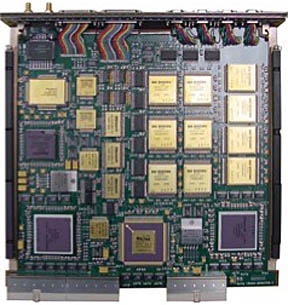


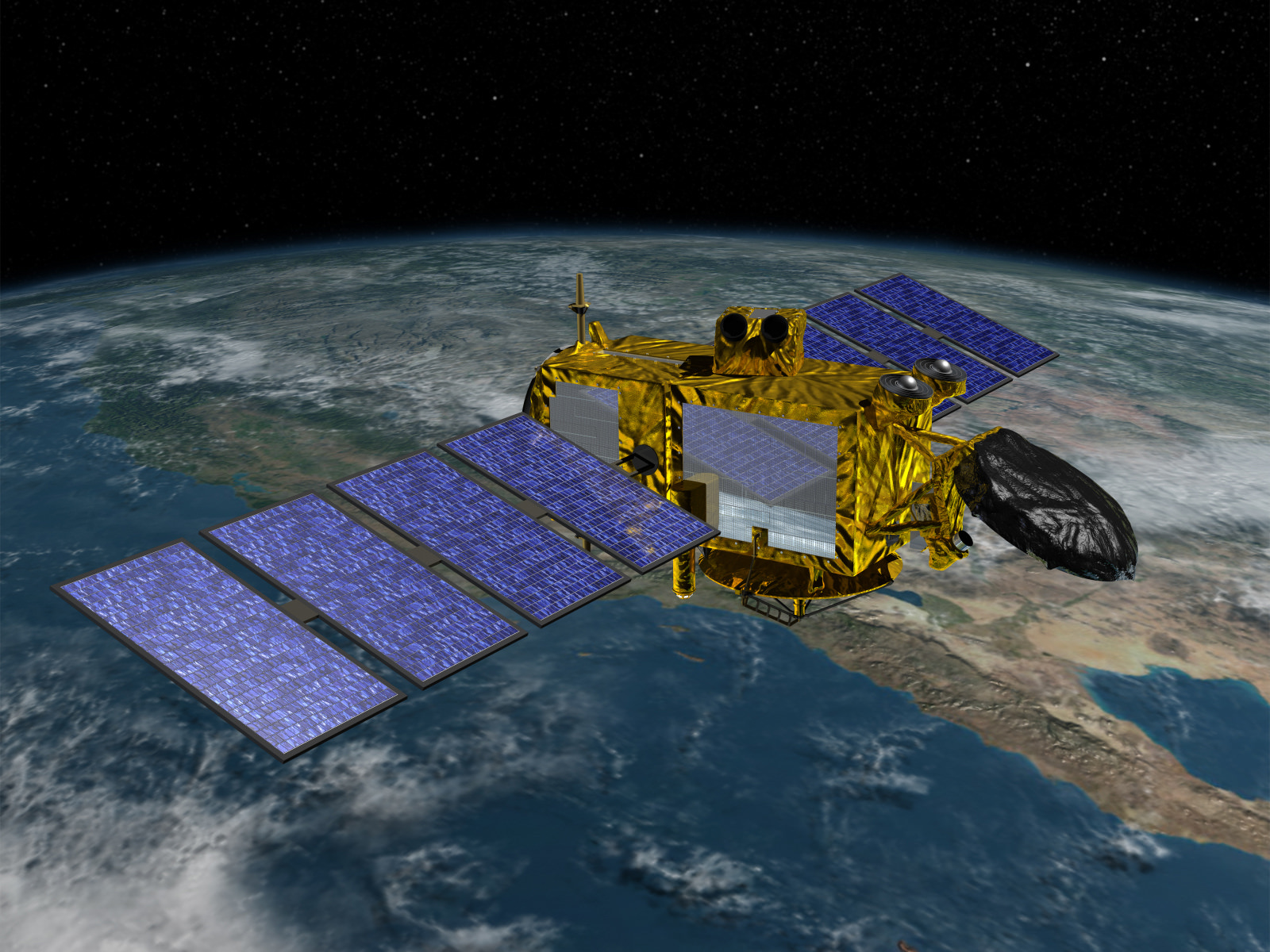

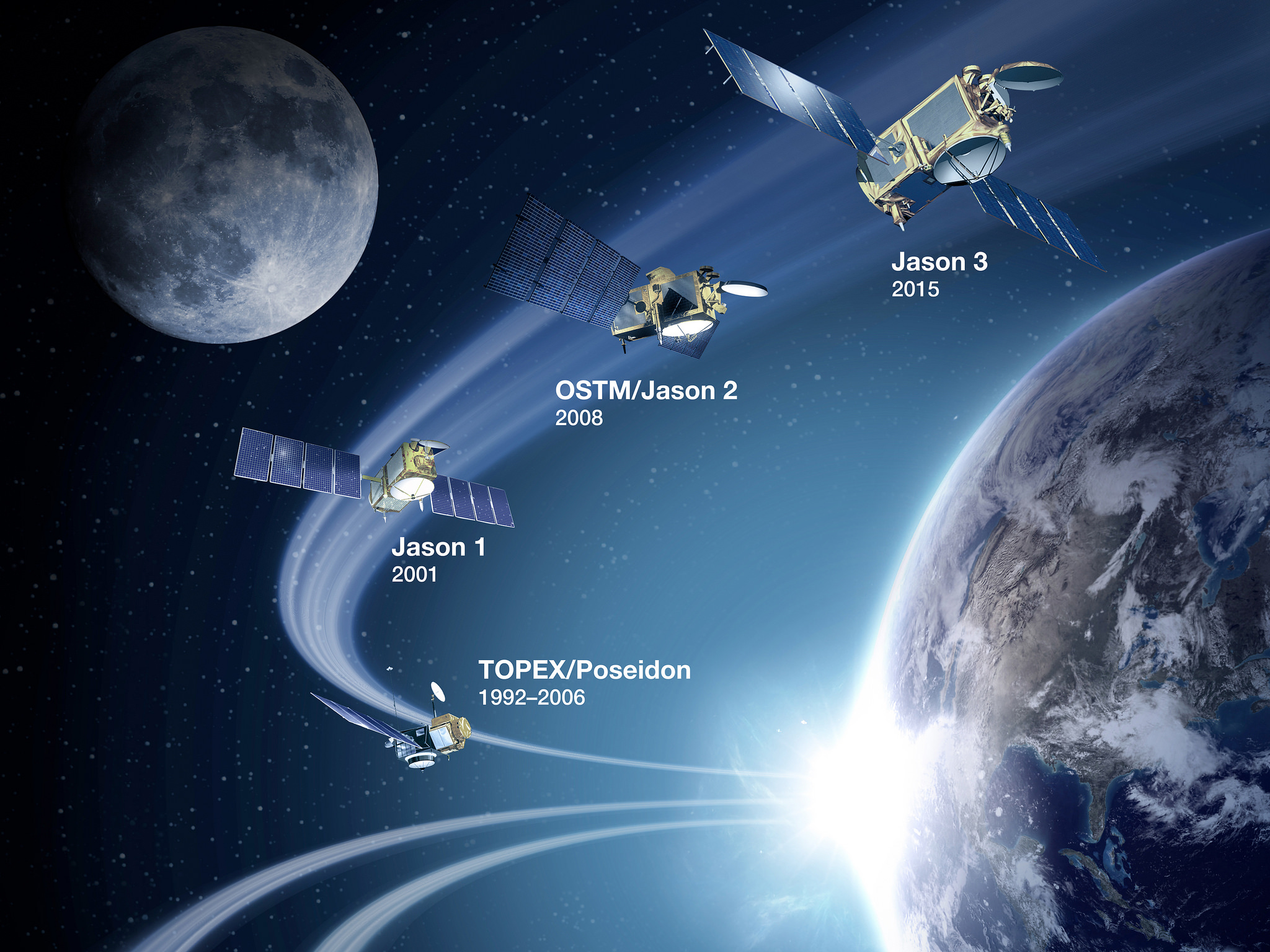
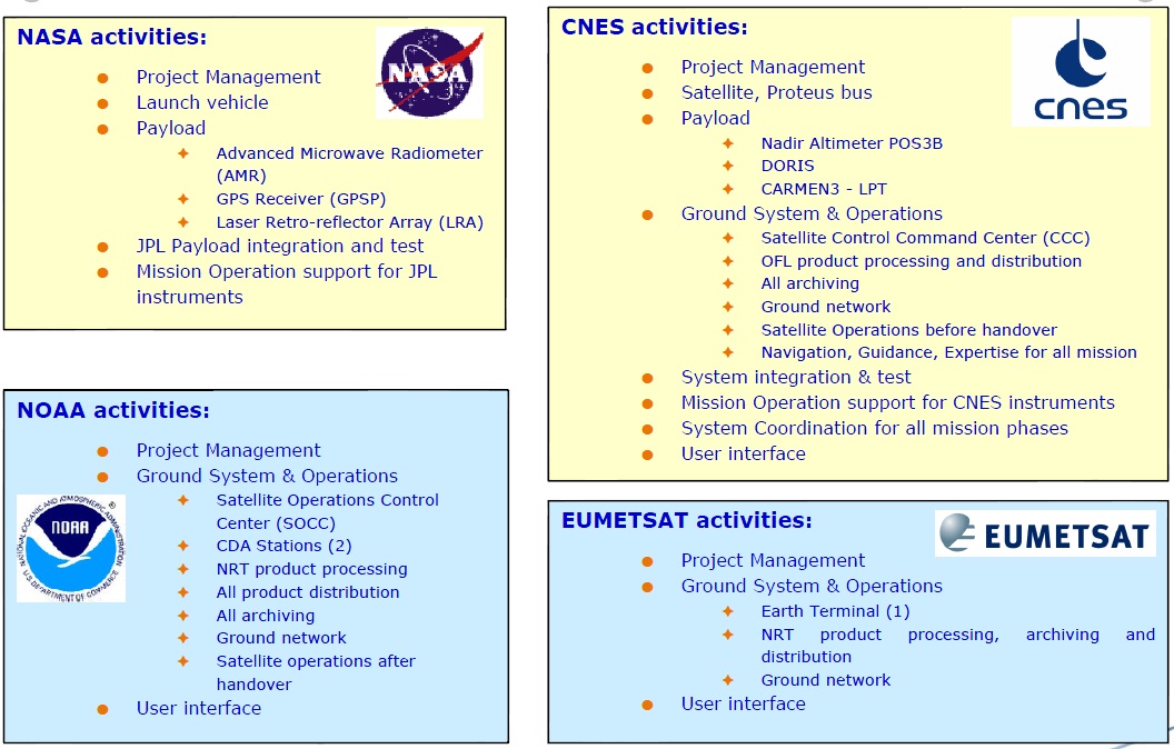
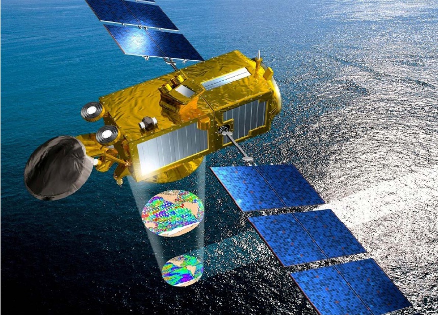


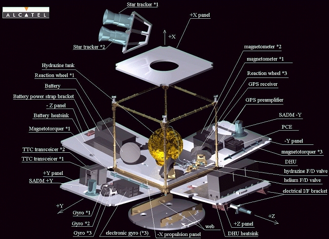
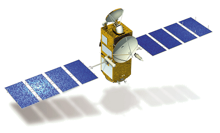


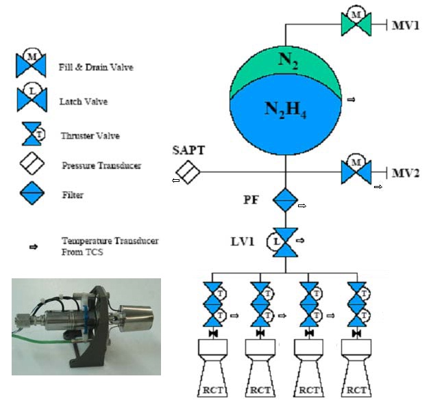
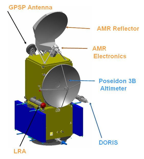
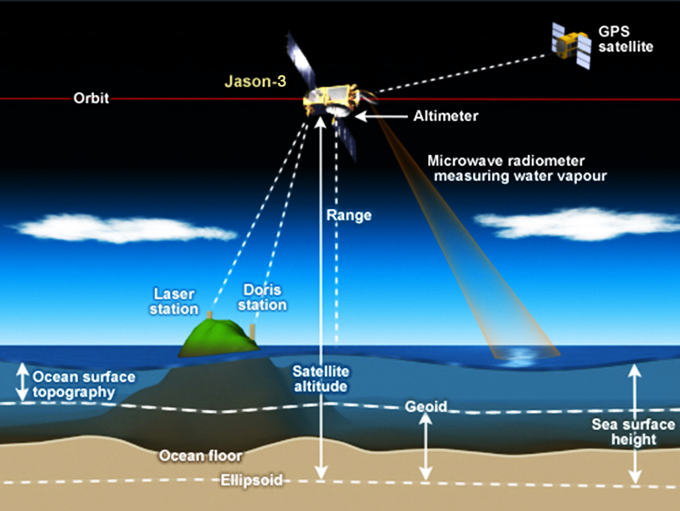
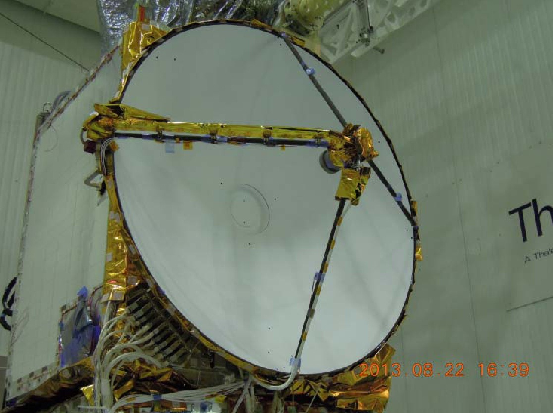
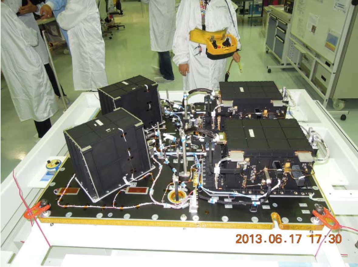
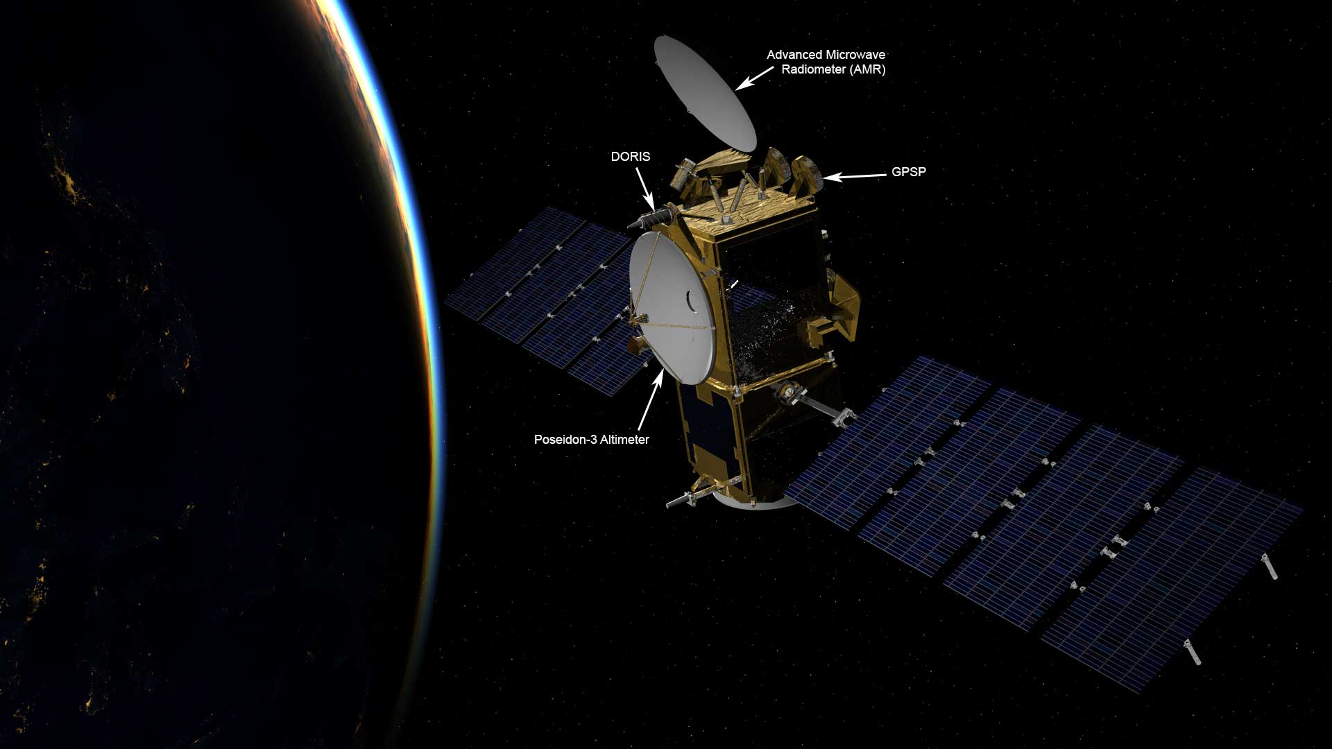
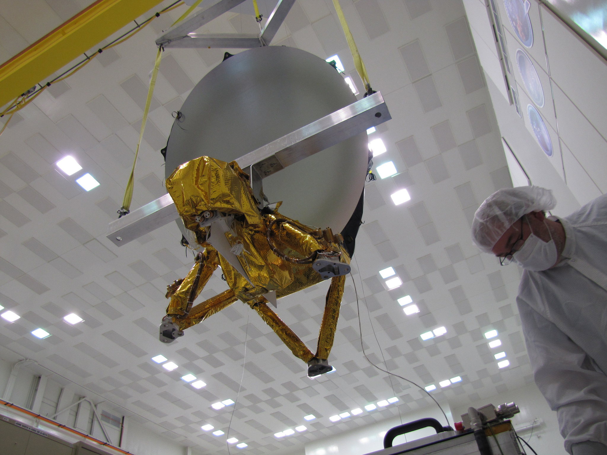
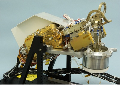
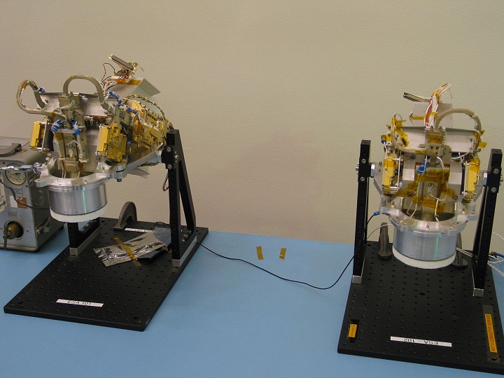

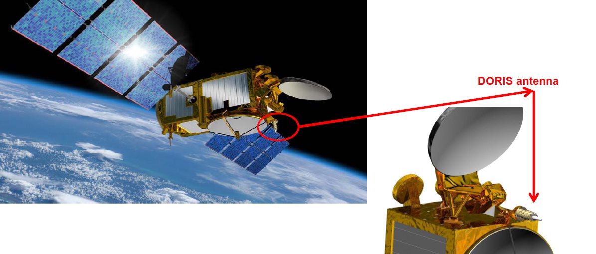
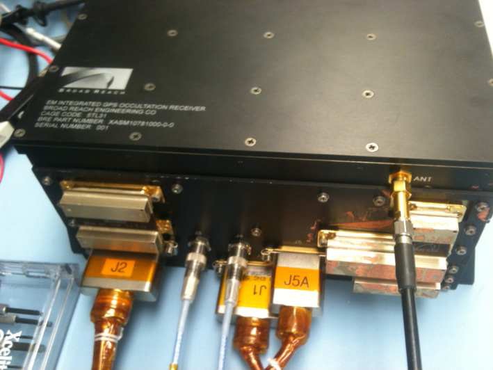
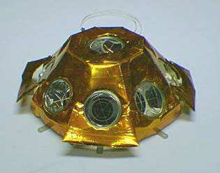

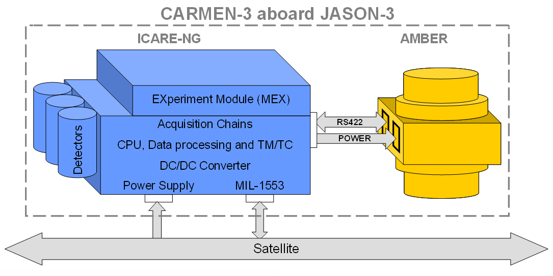


 Titled "SiGe Integrated Electronics for Extreme Environments," the $12 million, 63-month project was funded by the National Aeronautics and Space Administration (NASA). In addition to Georgia Tech, the 11-member team included academic researchers from the University of Arkansas, Auburn University, University of Maryland, University of Tennessee and Vanderbilt University. Also involved in the project were BAE Systems, Boeing Co., IBM Corp., Lynguent Inc. and NASA's Jet Propulsion Laboratory.

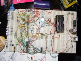
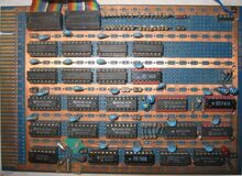


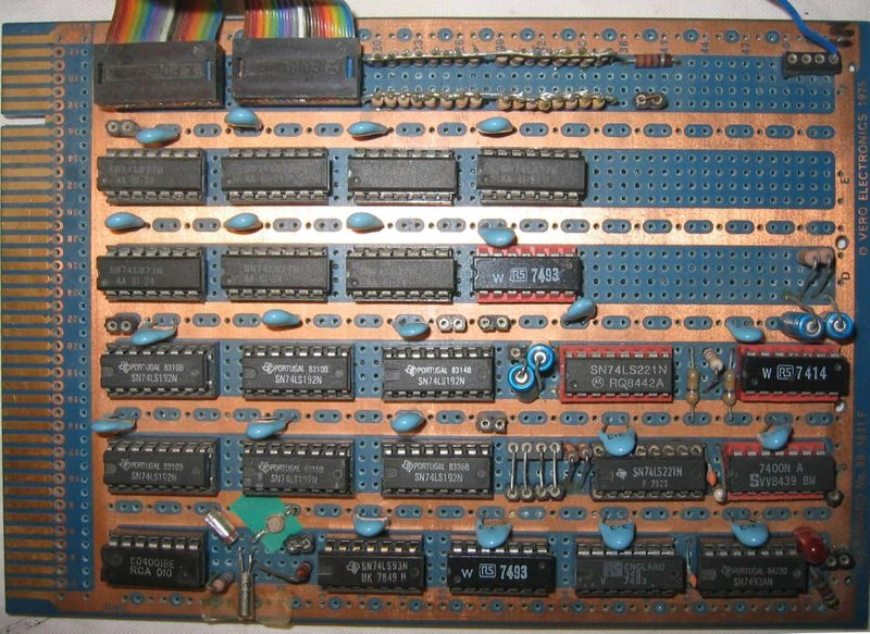


 Termoionics tube for radio and hi-fi applications Electric symbol of vacuum triode


 Transistor BJT NPN obtained from a semiconductor bar Symbol of the BJT NPN transistor (PNP is represented with reversed arrow)


nice article see this also Click here
BalasHapus