

In the electronics industry namely control and measurement the most important is knowledge and work from:
1. Voltage work information
2. Current work information
3. Frequency work information
4. Period work information
5. Work power information
6. Information on temperature work
7. Information on the work of the environmental climate
8. Information on the work of obstacles, resistance, resistance of electronic components
9. Work information on light intensity
10. Work information on electronic component power dissipation
11. Work information on inductive and capacitive reactances
This information is important so that an electronic device in terms of the quality of the material and its performance can be precisely and appropriately used and more purely in terms of secondary digital and primary digital insights, especially the signal changes from the primary and secondary time series.
How Filters Work
CR Filter Operation.
Figs 8.2.1 and 8.2.2 show two common methods of using C and R together to achieve alterations in AC signals. These CR combinations are used for many purposes in a wide variety of circuits. This section describes their effects when used as filters with sine wave signals of varying frequencies. The same circuits are also used to change the shape of non-sinusoidal waves, and the techniques used are described in Differentiators and Integrators later in this this module.
The High Pass CR Filter

Fig 8.2.1 High Pass CR Filter
The CR circuit illustrated in Fig 8.2.1, when used with sinusoidal signals is called the HIGH PASS FILTER. Its purpose is to allow high frequency sine waves to pass unhindered from its input to its output, but to reduce the amplitude of, (to attenuate) lower frequency signals. A typical application of this circuit would be the correction of frequency response (tone correction) in an audio amplifier.
As described in Module 6, resistance is constant at any frequency, but the opposition to current flow offered by the capacitor (C) however, is due to capacitive reactance XC, which is greater at low frequencies than at high frequencies.
The reactance of the capacitor (XC) and the resistance of the resistor (R) in fig 8.2.1 act as a potential divider placed across the input, with the output signal taken from the centre of the two components. At low frequencies where XC is much greater than R, the share of the signal voltage across R will be less than that across C and so the output will be attenuated. At higher frequencies, it is arranged, by suitable choice of component values, that the resistance of R will be much greater than the (now low) reactance XC, so the majority of the signal is developed across R, and little or no attenuation will occur.
The Low Pass CR Filter

Fig 8.2.2 Low Pass CR Filter
In Fig 8.2.2 the positions of the resistor and capacitor are reversed, so that at low frequencies the high reactance offered by the capacitor allows all, or almost all of the input signal to be developed as an output voltage across XC. At higher frequencies however, XC becomes much less than R and little of the input signal is now developed across XC. The circuit therefore attenuates the higher frequencies applied to the input and acts as a LOW PASS FILTER.
The band of frequencies attenuated by high and low pass filters depends on the values of the components. The frequency at which attenuation begins or ends can be selected by suitable component choices. In cases of audio tone correction, the resistor may be made variable, allowing a variable amount of bass or treble (low or high frequency) cut. This is the basis of most inexpensive tone controls
High and low pass filters can also be constructed from L and R. In this case the action is the same as for the CR circuit except that the action of XL is the reverse of XC. Therefore in LR filters the position of the components is reversed.
Phase Change in Filters
The above description of high and low pass filters explains how they operate in terms of resistance and reactance. It shows how gain (Vout/Vin) is different at high and low frequencies due to the relative values of XC and R. However this simple explanation does not take the phase relationships between capacitors or inductors, and resistors into account. To accurately calculate voltage values across the components of a filter it is necessary to take phase angles into consideration as well as resistance and reactance. This can be done by using phasor diagrams to calculate the values graphically, or by a branch of algebra using ´complex numbers´ and ´j Notation´. However these calculations can also be done using little more than the Reactance calculations learned in Module 6 and the Impedance Triangle calculations from Module 7.
Problem:

Calculate the peak to peak voltages Vr appearing across R and Vc appearing across C when an AC supply voltage of 2Vpp at 1kHz is applied to the circuit as shown.
Although C and R form a potential divider across Vs it is not possible to calculate these values using the potential divider equation(because phase angles must also be taken into account):

Follow these steps:
1. Find the value of capacitive reactance XC using:


2. Use the Impedance Triangle to find Z (the impedance of the whole circuit).


3. Knowing that the supply voltage Vs is developed across Z, the next step is to calculate the volts per ohm (V/Ω),

Because the volts per ohm will be the same for each component as it is for the circuit impedance, the result from step 3 can now be used to find the voltages across C, and across R.


If required, the Phase angle θ could also be found using trigonometry as described in Phasor Calculations, Module 5.4 (Method 3). To find the angle θ (the phase difference between the supply voltage VS and the supply current, which would be in the same phase as VR) the two voltages already found could be used.

Because circuits containing capacitance (or inductance) in addition to resistance affect the phase relationships of sine wave signals. This allows these same circuits to be used to change the PHASE of signals instead of, or as well as the amplitude.
CR Filter Operation
Fig 8.2.3 and Fig. 8.2.4 demonstrate how phasor diagrams can explain both the amplitude and phase effects of a CR filters. Adjust the frequency slider and notice that it is the input voltage that apparently changes phase, but this is just because the circuit current phasor (and therefore the VR phasor, which is always in phase with the current) is used as the static reference phasor. The thing to remember is that there is a phase change of between 0° and 90° happening between VIN and VOUT, which depends on the frequency of the signal.
Using phasor diagrams to explain the high pass filter shows that:
• In The High pass Filter (Fig. 8.2.3) at low frequencies the output VOUT (VR) is much smaller than VIN (VC) and a phase shift of up to 90° occurs with the output phase leading the input phase.
• At high frequencies there is little or no difference between the relative amplitudes of VOUT (VR) and VIN , and little or no phase shift is taking place. At the corner frequency the phase shift is 45° and below that the Bode plot shows that frequency gain falls off at a steady rate of -20dB per decade.
Fig 8.2.4 similarly demonstrates the action of a CR Low Pass Filter. In this circuit note that VOUT = VC so the output phase lags the input phase by up to about -90°, depending on the input frequency .
Bode Plots
Showing Phase Shift and Attenuation
When considering the operation of filters, the two most important characteristics are:
- • The FREQUENCY RESPONSE, which illustrates those frequencies that will, and will not be attenuated.
- •The PHASE SHIFT created by the filter over its operating range of frequencies.
Bode Plots show both of these characteristics on a shared frequency scale making a comparison between the gain of the filter and the phase shift simple and accurate.
Frequency is plotted on the horizontal axis using a logarithmic scale, on which every equal division represents ten times the frequency scale of the previous division, this allows for a much wider range of frequency to be displayed on the graph than would be possible using a simple linear scale. Because the frequency scale increases in "Decades" (multiples of x10) it is also a convenient way to show the slope of the gain graph, which can be said to fall at 20dB per decade.
The vertical axis of the gain graph is marked off in equal divisions, but uses a logarithmic unit, the decibel (dB) to show the gain, which with simple passive filters is always unity, or a gain ratio of 1, (which corresponds to 0dB on the logarithimic Decibel scale) or less. The dB units therefore have negative values indicating that the output of the filter is always less than the input, (a gain of less than 1). The upper section of the vertical axis is plotted in degrees of phase change, varying between 0 and 90° or sometimes between −90° and +90°

Fig 8.3.1 Bode Plot for a Low Pass Filter.
A Bode plot for a low pass filter is shown in Fig 8.3.1. Note the point called the corner frequency. This is the approximate point at which the filter becomes effective. Frequencies below this point are unaffected by the filter, while above the corner frequency, attenuation of the signal increases at a constant rate of 6dB per octave. This means that the signal output voltage is halved (−6dB) for each doubling (an octave) of the input frequency.
Alternatively the same fall off in gain may be labelled as −20dB per decade, which means that voltage gain falls by ten times (to 1/10 of its previous value) for every decade (tenfold) increase in frequency. The fall off in gain of a filter is quite linear beginning from the corner frequency (also called the cut off frequency). I.e. if the voltage gain of a low pass filter is 1 at a frequency of 1kHz, it will be 0.1 at 10kHz. The linear fall off in gain is common to both high and low pass filters, it is just the direction of the fall, increasing or decreasing with frequency, that is different.
The corner (or cut off) frequency (ƒC) is where the active part of the gain plot begins, and the gain has fallen by −3dB. The phase lag of the output signal in a low pass filter (or phase lead in a high pass filter) is at 45°, exactly half way between its two possible extremes of 0° and 90° The corner frequency may be calculated for any two values of C and R using the formula:

For LR filters the formula is:

Note that the corner frequency is that point where two straight lines representing the two sections of the graph either side of ƒC would intersect. The actual curve makes a smooth transition between the horizontal and sloping sections of the graph and the gain of the filter is therefore -3dB at ƒC .
Differentiators
A simple RC network such as the high pass filter illustrated in Fig. 8.4.1, when used with non sinusoidal waves produces a change in wave shape at its output. With a sine wave input, only the amplitude and phase of the wave change. However, if the input wave is a complex wave, such as a square or triangular wave, the effect of these simple circuits appears to be quite different.

Fig.8.4.1 The Differentiator Circuit
Differentiation

Fig 8.4.2 Differentiation.
The circuit is called a DIFFERENTIATOR because its effect is very similar to the mathematical function of differentiation, which means (mathematically) finding a value that depends on the RATE OF CHANGE of some quantity. The output wave of a DIFFERENTIATOR CIRCUIT is ideally a graph of the rate of change of the voltage at its input. Fig. 8.4.2 shows how the output of a differentiator relates to the rate of change of its input, and that actually the actions of the high pass filter and the differentiator are the same.
Because the differentiator output is effectively a graph showing the rate of change of the input, whenever the input is changing rapidly, a large voltage is produced at the output. The polarity of the output voltage depends on whether the input is changing in a positive or a negative DIRECTION.
Sine Waves
A graph of the rate of change of a sine wave is another sine wave that has undergone a 90° phase shift (with the output wave leading the input wave).
Square Waves
The square wave input and output in Fig 8.4.2 shows the ideal differentiator action of a high pass filter. The output wave is now nothing like the input wave, but consists of narrow positive and negative spikes. The positive spike coincides in time with the rising edge of the input square wave. The negative spike of the output wave coincides with the falling, or negative going (towards zero volts) edge of the square wave. Notice that the DC level of the wave is also changed by the differentiator. The output wave now has both positive and negative half cycles above and below a centre line of zero volts, due to the dc blocking effect of the capacitor.
Triangular Waves
A triangular wave has a steady positive going rate of change as the input voltage rises, so produces a steady positive voltage at the output. As the input voltage falls at a steady rate of change, a steady negative voltage appears at the output. The graph of the rate of change of a triangular wave is therefore a square wave. Wave shaping using a simple high pass filter or differentiator is a very widely used technique, used in many different electronic circuits.
Practical Differentiation

Fig 8.4.3 Practical Differentiation.
Although the ideal situation is shown in Fig. 8.4.2, how closely the output resembles perfect differentiation depends on the frequency (and therefore periodic time) of the input wave and the time constant of the components used, as shown in Fig. 8.4.3. The high pass filter works as a differentiator when the input is:
a. A non-sinusoidal wave.
b. The time constant(T) of the input wave is much greater (longer duration) than the time constant(CR) of the circuit (T>>CR), i.e. at relatively low frequencies.
When T is less than or equal to CR (T<=CR) the output wave shape will be less than an ideally differentiated wave shape, being more or less like the waveforms shown in the bottom row of Fig. 8.4.3.
Although passive (with no amplification) differentiators are cheap and efficient, where it is necessary to control the amplitude of the output, active differentiators using op-amps .
Integrators
The Integrator Circuit
Integration is used extensively in electronics to convert square waves into triangular waveforms, in doing this it has the opposite effect to differentiation (described in Filters & Wave shaping Module 8.4). The shape of the input wave of an integrator circuit in this case will be a graph of the rate of change of the output wave as can be seen by comparing the square wave input and output waveforms in Fig. 8.5.2. Notice that the integrator circuit (shown in Fig. 8.5.1) is that of the CR low pass filter .

Fig. 8.5.1 The Integrator (also low-pass filter) Circuit.
Integrator Action with a Sine Wave Input

Fig. 8.5.2 Integrator Action
If the input is a sine wave, the circuit does not act as an integrator, but as a simple low pass filter (LPF) where the amplitude of the output wave is reduced, and its phase relative to the input wave is shifted so that it lags by up to -90° dependant on the frequency of the wave and the CR time constant of the circuit, as described in Filters & Wave shaping Module 8.2
The low pass filter circuit is therefore called an integrator only when:
a. The input wave is a square wave.
b. The periodic time(T) of the input wave is much shorter than the circuit time constant(CR) i.e.(T<=CR).
Provided that these conditions are met, then the action of the integrator is opposite to that of the differentiator circuit described in Filters and Wave shaping Module 8.4.
Integration of a Square Wave
With a square wave input and the correct relationship between the periodic time of the wave and the time constant of the circuit, Fig 8.5.2 shows that integration takes place. The output is now (considering the waveforms as simple graphs), a graph of the changing area beneath the input wave. The integrator has converted the square wave input to a triangular wave at the output, the slope of this wave describes the increase in area beneath the square wave (moving from left to right). For the circuit to act effectively as an integrator, the periodic time of the wave must be similar to, or shorter than the circuit time constant i.e. (T<=CR). The higher the frequency of the input wave for a particular time constant, the better the shape of the output wave will be, but the smaller its amplitude.
At lower frequencies, where the periodic time T of the wave is much longer than the time constant of the circuit CR (T>>CR), some change in wave shape does occur, but the output does not conform to the definition of an integrator; the circuit has just rounded the rapid vertical transitions of the square wave. The output at these low frequencies is not a graph of the changing area beneath the input wave, the circuit is acting as a low pass filter and removing the high frequency components of the square wave that were responsible for the rapid vertical changes at each half cycle.
Action on a Triangular Wave
When the input to the integrator circuit is a triangular wave, the output seems to become a sine wave. Remember however, that the integrator circuit is also a low pass filter that has the effect of removing the higher frequency harmonics present in the complex (triangular) wave at its input, leaving just the fundamental (sine wave) and possibly a few lower frequency harmonics. At low frequencies, the output from the integrator circuit is therefore a rounded form of the triangular input wave.
The main purpose of a passive CR integrator is to produce a good triangular wave shape from a square wave input, which it can do very well and at very low cost (only two components are needed) although the output will be reduced in amplitude.
What is the difference between active filter and passive filter applications?
Passive filters contains passive components (R,L,C), they do not depend upon an external power supply and/or they do not contain active components such as transistors or battery. The simplest passive filters, RC and RL filters, include only one reactive element, except HYBRIED LC Filter which is characterized by inductance and capacitance integrated in one element.
Active filters are implemented using a combination of passive and active (amplifying) components, and require an outside power source. operational filters are frequently used in active filter designs. These can have high Q Factor, and can achieve resonance without the use of inductors. However, their upper frequency limit is limited by the bandwidth of the amplifiers. The most common types of active filters are classified into four such as 1.Butterworth 2.Chebyshev 3.Bessel 4.Elliptical
The difference between Active and Passive Filters
1. Passive filters consume the energy of the signal, but no power gain is available; while active filters have a power gain.
2. Active filters require an external power supply, while passive filters operate only on the signal input.
3. Only passive filters use inductors.
4. Only active filters use elements kike op-amps and transistors, which are active elements.
5. Theoretically, passive filters have no frequency limitations while, active filters have limitations due to active elements.
6. Passive filters have a better stability and can withstand large currents.
7. Passive filters are relatively cheaper than active filters.
Applications of Active filters
- Active filters are used in communication system for suppressing noise to isolate a communication of signal from various channels to improve the unique message signal from a modulated signal.
- These filters are used in instrumentation systems by the designers to choose a required frequency apparatus and detach unwanted ones.
- These filters can be used to limit the analog signals bandwidth before altering them to digital signals.
- audio systems by engineers to send various frequencies to various speakers. For example, in the music industry, record & playback applications are needed to control the frequency components.
- Active filters are used in biomedical instruments to interface psychological Sensors with diagnostic equipments & data logging.
Applications of Passive filters
- low pass filters Woofers for low frequency, and Tweeters for high frequency reproduction). In this application the combination of high and low pass filters is called a "crossover filter".
- high pass filters especially audio amplifiers
- band pass filters while rejecting signals at all frequencies above and below this band
- band stop filters older radio and TV receivers
- I.F Transformers found in older in radio and TV equipment to pass a band of radio frequencies from one stage of the intermediate frequency (IF) amplifiers.
XO___XO Active Filters for Video
Originally, video filters were passive LC circuits surrounded by amplifiers. Smaller, more efficient designs can currently be achieved by combining the amplifier with an RC filter. Sensitivity analysis and predistortion methods developed in the 1960s have, moreover, overcome the poor performance that gave early video filters a bad reputation.
High-performance op amps and specialized software for the PC enable the design of wide-bandwidth active filters, but those advantages do not address the requirements of any specific application. For video filters, the particular application and signal format add nuance to each circuit design. The two major video applications follow.
Antialiasing filters: These devices are placed before an analog-to-digital converter (ADC) to attenuate signals above the Nyquist frequency, which is one half the sample rate of the ADC. These filters are usually designed with the steepest possible response to reject everything above the cutoff frequency¹. For ITU-601 applications and others, such performance is achieved using analog filters combined with digital filters and an oversampling ADC. For applications such as PC graphics, very little filtering is required.
Reconstruction filters: Also called (sinx)/x or zero-order-hold correctors, these filters are placed after a digital-to-analog converter (DAC) to remove multiple images created by sampling, though not to remove the DAC clock. Reconstruction filters are seldom as selective as antialiasing filters, because the DAC's hold function also acts as a filter—an action that lowers the required selectivity, but introduces loss in the response. The available video formats are RGB, component video, composite video, and RGB PC graphics.
All applications and formats require a video filter to be "phase linear," a condition specified by the parameter called group delay (delay vs. frequency). The degree of phase linearity required depends on the application and the video format. For example, antialiasing filters and component formats are more tightly specified than are reconstruction applications and composite video. Requirements for the various applications and formats are specified by NTSC, PAL/DVB, ITU, SMPTE, and VESA.
This article compares different filters to determine the optimum design for a given application or format. Rauch and Sallen-Key realizations are compared for their GBW-to-cutoff ratios, using predistortion and element sensitivity techniques to achieve accuracy in the design. Those filters to be considered are:
- An ITU-601 antialiasing filter
- A 20MHz antialiasing and reconstruction filter
- An HDTV reconstruction filter
Filters and Their Characteristics
Whether used for antialiasing or reconstruction, the filter must have a lowpass characteristic to pass the video frame rate. One should, therefore, be wary of AC-coupling. Lowpass filters are categorized by their amplitude characteristic or by the name of the polynomial that describes it (Bessel, Butterworth, Chebyshev, or Cauer). Figure 1 shows these characteristics normalized to a 1-rad bandwidth. Typically, a filter with the best selectivity and the minimum number of poles (to minimize cost) would be chosen, but the additional need for phase linearity limits the available choices.

Figure 1. Amplitude and group delay vs. frequency for various filter types are normalized to a 1-rad bandwidth.
Figure 1. Amplitude and group delay vs. frequency for various filter types are normalized to a 1-rad bandwidth.
Phase Linearity and Group Delay
A filter's phase linearity is specified as envelope delay or group delay (GD) versus frequency. A flat group delay indicates all frequencies are delayed by the same amount, which preserves the shape of the waveform in the time domain. Thus, absolute group delay is not as important as the variation in group delay. A separate specification called channel-to-channel variation, which is specified as "time coincidence," should not be confused with group delay.
Though not desirable for video, how much group-delay variation is acceptable, and why? The answer depends on the application and the video format. For example, ITU-470 specifies group delay very loosely for composite video. However, ITU-601 specifies it tightly to ensure generational stability, both for MPEG-2 compression and to control phase jitter before serialization. So, what filter characteristics are considered necessary to ensure phase linearity?
The group-delay curves in Figure 1 show a peak near the cutoff frequency (ω/ωc = 1). That is a problem caused by the steep phase change near the cutoff frequency. To get an idea of scale, a 3-pole, 6MHz Butterworth filter has a group-delay variation of 20ns to 25ns over its bandwidth. Increasing the number of poles or the filter's selectivity increases that variation. Other, more exotic filters² used to minimize group-delay variation include Bessel, phase approximation, Thompson-Butterworth, and LeGendre. Nevertheless, the Butterworth characteristic is most often used for video.
Group-Delay Problems with Component Video
All formats and applications are sensitive to group-delay variation. The degree of sensitivity depends on the number of signals and their bandwidths. Composite NTSC/PAL has only one signal, with group delay specified in ITU-470. Those requirements are easily met. RGB and component video each have multiple signals. The RGB signals have equal bandwidths while component-video signals do not, making group-delay matching easy with RGB, but difficult with component video.
Because Pb and Pr signals have half the bandwidth of the luma (Y) signal, their group delay is double that of the Y signal³. One solution is to slow down the Y signal by adding delay stages. Another solution is to equalize bandwidths by doubling the sample rates of Pb and Pr, which raises the 4:2:2 sampling rate to 4:4:44, allowing the signal to be treated as RGB. The additional Pb and Pr samples are discarded during antialiasing or averaged in reconstruction applications.
The other component-video format, S-VHS, can be somewhat confusing. The Y channel is the same as in YPbPr, but the chroma signal (C) looks like it should be bandpass filtered rather than lowpass filtered. As for YPbPr signals, bandpass filtering causes group-delay and timing problems and, therefore, should not be implemented. Unless analog encoding is done, Y and C can be lowpass filtered with the same filter. S-VHS is more forgiving of bandwidth than of problems caused by trying to equalize the delay. S-VHS is typically seen in reconstruction applications, for which the main concern is correct timing between Y and C.
Choosing an Op Amp
After choosing a filter characteristic, the next step is to implement it with an actual circuit. The most commonly used, single-op-amp circuits are the Sallen-Key configuration in noninverting form and the Rauch configuration in inverting form. An important consideration for op amps operating in the wide bandwidths of video applications is the minimum gain-bandwidth (GBW). Video signals are large, typically 2VP-P, so the large-signal GBW is referenced. This parameter is not to be confused with the 2VP-P 0.1dB GBW, which is much lower.
For filter circuits, how much larger than the filter's cutoff frequency does the op amp GBW have to be? For a Rauch (inverting) filter, the phase argument of the characteristic is:
Arg[K(jω)]inv = -(ωc/GBWrad)(1 + Rf/Ri)
For a Sallen-Key (noninverting) filter:
Arg[K(jω)]noninv = π-(ωc/GBWrad)(1 + Rf/Ri)
where Rf and Ri are the gain-set resistors in Ω, GBWrad is the op amp's gain-bandwidth product, and ωc is the filter's cutoff frequency in radians per second. Set the gain by introducing values for Rf and Ri5, and solve for (ωc/GBWrad). A unity-gain Rauch circuit has Rf/Ri = 1, and a Sallen-Key circuit has Rf/Ri = 0. Thus, for the same phase error, a Sallen-Key requires half the GBW of a Rauch circuit. As the required gain increases, they converge and leave little advantage for the Sallen-Key in terms of GBW, but other issues must be considered as well.
Predistortion, Bandwidth, Q, and Element Sensitivity
Anything less than an infinite GBWrad/ωc ratio causes the closed-loop poles of a filter to move. That is why an actual filter often exhibits a lower bandwidth (ωc) than does the paper design6. This can be compensated for by increasing the design bandwidth, which is known as predistortion. Formulas for the Sallen-Key and Rauch circuits (listed in Tables 1 and 2) allow us to calculate a design bandwidth that provides the actual bandwidth needed. Component tolerance must then be taken into account.
To determine component tolerance, a sensitivity function7 is needed: SXY gives the ratio between a change in the value of part X and the consequent change in parameter Y. For example, Table 1 shows that the Q in a Sallen-Key circuit (vs. a Rauch circuit) has a large sensitivity to variations in C1 and C2. That means a Sallen-Key is less tolerant of parasitics than is a Rauch. The point is that SXY lets the effect be predicted, and then the design can be created accordingly. Next, some typical designs are considered.
Table 1. Component sensitivities including BW and Q predistortion formulas (Sallen-Key realization, ωO = 1rad/s)
| Sensitivity Function SXY | Gain K = 3 - 1/Q (R1 = R2 = C1 = C2 = 1) | Gain K = 1 (R1 = R2 = 1) | Gain K = 2 (R1 = C1 = 1) |
| SXω (x = R1, R2, C1, C2) | -1/2 | -1/2 | -1/2 |
| SKQ | 14 | 50 | 10 |
| SR1Q | 4.5 | 0 | 4.5 |
| SR2Q | -4.5 | 0 | -4.5 |
| SC1Q | 9.5 | 1/2 | 5.5 |
| SC2Q | -9.5 | -1/2 | -5.5 |
| SRaK | -9/14 | N/A | -1/2 |
| SRbK | 9/14 | N/A | 1/2 |
| ωc (actual) | ωc (design) | ωc (design) | — |
| Q (actual) | Q (design) | Q (design) | — |
Table 2. Component sensitivities including BW and Q predistortion formulas (Rauch realization, ωO = 1rad/s)
| Sensitivity Function SXY | Gain K = 1 (R1 = R2 = R3 = 1) | Gain K = 2 (R1 = 1, R3 = Ho, R2 = (Ho / 1 + Ho)) | Gain K = 2 (C1 = 1, C2 = C1 / 100) |
| SXω (x = R1, R2, C1, C2, SR1ω = 0) | -1/2 | -1/2 | -1/2 |
| SR1Q | 1/3 | 1/3 | 1/3 |
| SR2Q | -1/6 | 0 | 0 |
| SC1Q | 1/2 | 1/2 | 1/2 |
| SC2Q | -1/2 | -1/2 | -1/2 |
| SR3K | 1 | 1 | 1 |
| SR1K | -1 | -1 | -1 |
| SR3Q | 1/6 | 0 | 0 |
| ωc (actual) | ωc (design) | — | — |
| Q (actual) | Q (design) | — | — |
Design of Antialiasing Filters
For antialiasing filters, selectivity is determined by a template for ITU-601 like the one in Figure 2. The specified bandwidth is 5.75MHz ±0.1dB, with an insertion loss of 12dB at 6.75MHz and 40dB at 8MHz, and with a group-delay variation of ±3ns over the 0.1dB bandwidth. Such performance is too difficult for an analog filter alone, but 4x oversampling modifies the requirements to 12dB at 27MHz and 40dB at 32MHz.

Figure 2. This filter template illustrates antialiasing requirements in accordance with the ITU-R BT.601-5 standard.
Using software or normalized curves8, one can find that a 5-pole Butterworth filter with -3dB bandwidth of 8.45MHz satisfies the requirement for selectivity, though not for group delay. For the latter, a delay stage is needed, for which the important op-amp parameter is the 0.1dB, 2VP-P bandwidth9. That number should be used in equations 1 and 2 to get an accurate design. A schematic for this application, with curves showing its gain and group-delay characteristics, is based on 4x oversampling (Figures 3a and 3b).

Figure 3. This schematic (a) and output response (b) represent a 5-pole, 5.75MHz Butterworth filter for ITU-601 antialiasing, using a Rauch circuit with a delay equalizer.
PC video is considered next. VESA does not specify templates for antialiasing or reconstruction filters. The XGA resolution (1024 x 768 at 85Hz) has a sampling rate of 94.5MHz and a Nyquist frequency of 47.25MHz. For> 35dB attenuation at the Nyquist frequency, a Rauch realization of a 20MHz, 4-pole Butterworth filter (Figures 4a and 4b) is used. Again, the MAX4450/MAX4451 are chosen for their excellent transient response and large-signal bandwidth (175MHz at 2VP-P).

Figure 4. This schematic (a) and output response (b) depict a 4-pole, 20MHz Butterworth filter for XGA graphics antialiasing, using a Rauch circuit.
Figure 2. This filter template illustrates antialiasing requirements in accordance with the ITU-R BT.601-5 standard.
Using software or normalized curves8, one can find that a 5-pole Butterworth filter with -3dB bandwidth of 8.45MHz satisfies the requirement for selectivity, though not for group delay. For the latter, a delay stage is needed, for which the important op-amp parameter is the 0.1dB, 2VP-P bandwidth9. That number should be used in equations 1 and 2 to get an accurate design. A schematic for this application, with curves showing its gain and group-delay characteristics, is based on 4x oversampling (Figures 3a and 3b).
Figure 3. This schematic (a) and output response (b) represent a 5-pole, 5.75MHz Butterworth filter for ITU-601 antialiasing, using a Rauch circuit with a delay equalizer.
PC video is considered next. VESA does not specify templates for antialiasing or reconstruction filters. The XGA resolution (1024 x 768 at 85Hz) has a sampling rate of 94.5MHz and a Nyquist frequency of 47.25MHz. For
Figure 4. This schematic (a) and output response (b) depict a 4-pole, 20MHz Butterworth filter for XGA graphics antialiasing, using a Rauch circuit.
Reconstruction Filters
Reconstruction filtering after a DAC is among the more poorly understood applications. Some designers think reconstruction filters are introduced to remove the sample clock, but nothing is further from the truth. When a signal is sampled, the samples are composed of multiple recurring signal images centered on harmonics of the sample clock. A reconstruction filter removes all but the baseband sample. If the antialiasing filter has served its purpose, the DAC output looks like image A in Figure 5, and then all samples to the right of it should be removed. Thus, reconstruction is similar to antialiasing except that, because each sample exists only for an instant, the DAC holds each for one clock period, thereby creating the familiar staircase approximation to a sloping line.

Figure 5. A typical DAC output spectrum is shown in terms of the sampling (FS) and Nyquist (FN) frequencies.
The hold function corresponds to a digital filter whose characteristic10 is similar to that of a Butterworth or Bessel filter (Figure 6). Notice that the response is decreased by 4dB at half the sample frequency. The second objective of a reconstruction filter is to restore that loss, which requires an amplitude equalizer like the circuit shown in Figure 7a. The equalizer is based on a delay stage and has a response like a Bessel filter. It can be designed from the DAC sample rate (Fs). Figure 7b shows the DAC's frequency response with and without an amplitude equalizer. Like the delay stage, it can be included in any reconstruction filter.

Figure 6. The "hold" function of a DAC produces a (sinx)/x response with nulls at multiples of the sampling frequency.

Figure 7. A DAC output (b) is shown with and without the (sinx)/x correction provided by an amplitude equalizer circuit (a).
The hold response also has a pole centered on the sample clock, which completely removes the clock. Nevertheless, most reconstruction applications refer to clock attenuation as a figure of merit. Now that the function of a reconstruction filter is understood, one can be designed.
The most common requirement for NTSC/PAL reconstruction is an attenuation of > 20dB at 13.5MHz and> 40dB at 27MHz, where ωc depends on the applicable video standard. A 3-pole Butterworth with Sallen-Key configuration is chosen for two reasons. First, its gain (+2) drives a back-terminated cable. Second, the group-delay variation can be adjusted to optimize performance without a delay equalizer. (Figures 8a–8d show NTSC and PAL designs, including gain and group-delay characteristics.) These applications usually include digital amplitude correction for the DAC, which can easily be added, if necessary.

Figure 8. For reconstruction filters with group-delay adjustment, the PAL version (a) has the amplitude and group-delay responses shown in (c), and the NTSC version (b) has the amplitude and group-delay responses shown in (d).
Illustrating a circuit for XGA, a 20MHz, 3-pole Butterworth filter in the Sallen-Key configuration includes the Figure 8 circuit for amplitude correction (Figures 9a and 9b). Complementing the antialiasing filter of Figure 4, this filter has a gain of +2 to drive a back-terminated 75Ω coaxial cable.

Figure 9. This 3-pole, 20MHz Butterworth filter for XGA reconstruction (a) includes (sinx)/x compensation. Its output response is shown in (b).
The last application is a reconstruction filter for HDTV. Based on the templates in the SMPTE 274 and 296M, it has a center frequency of ωc = 0.4 x FS = 29.7MHz. Amplitude correction for the DAC is usually included, but group-delay compensation must be added. The resulting 30MHz, 5-pole Sallen-Key filter (Figure 10) has > 40dB attenuation at 74.25MHz, as well as a group-delay stage with a +2 gain to drive a back-terminated 75Ω coaxial cable.

Figure 10. A 5-pole, 30MHz reconstruction filter for HDTV includes amplitude correction for the DAC.
Figure 5. A typical DAC output spectrum is shown in terms of the sampling (FS) and Nyquist (FN) frequencies.
The hold function corresponds to a digital filter whose characteristic10 is similar to that of a Butterworth or Bessel filter (Figure 6). Notice that the response is decreased by 4dB at half the sample frequency. The second objective of a reconstruction filter is to restore that loss, which requires an amplitude equalizer like the circuit shown in Figure 7a. The equalizer is based on a delay stage and has a response like a Bessel filter. It can be designed from the DAC sample rate (Fs). Figure 7b shows the DAC's frequency response with and without an amplitude equalizer. Like the delay stage, it can be included in any reconstruction filter.
Figure 6. The "hold" function of a DAC produces a (sinx)/x response with nulls at multiples of the sampling frequency.
Figure 7. A DAC output (b) is shown with and without the (sinx)/x correction provided by an amplitude equalizer circuit (a).
The hold response also has a pole centered on the sample clock, which completely removes the clock. Nevertheless, most reconstruction applications refer to clock attenuation as a figure of merit. Now that the function of a reconstruction filter is understood, one can be designed.
The most common requirement for NTSC/PAL reconstruction is an attenuation of > 20dB at 13.5MHz and
Figure 8. For reconstruction filters with group-delay adjustment, the PAL version (a) has the amplitude and group-delay responses shown in (c), and the NTSC version (b) has the amplitude and group-delay responses shown in (d).
Illustrating a circuit for XGA, a 20MHz, 3-pole Butterworth filter in the Sallen-Key configuration includes the Figure 8 circuit for amplitude correction (Figures 9a and 9b). Complementing the antialiasing filter of Figure 4, this filter has a gain of +2 to drive a back-terminated 75Ω coaxial cable.
Figure 9. This 3-pole, 20MHz Butterworth filter for XGA reconstruction (a) includes (sinx)/x compensation. Its output response is shown in (b).
The last application is a reconstruction filter for HDTV. Based on the templates in the SMPTE 274 and 296M, it has a center frequency of ωc = 0.4 x FS = 29.7MHz. Amplitude correction for the DAC is usually included, but group-delay compensation must be added. The resulting 30MHz, 5-pole Sallen-Key filter (Figure 10) has > 40dB attenuation at 74.25MHz, as well as a group-delay stage with a +2 gain to drive a back-terminated 75Ω coaxial cable.
Figure 10. A 5-pole, 30MHz reconstruction filter for HDTV includes amplitude correction for the DAC.
Practical Aspects of Active Video-Filter Design
Whether filters are designed by hand, with the aid of software, or with a combination of these approaches, the actual response may not be exactly what is wanted. One cause is the discrepancy between a calculated response and the actual response obtained using standard component values.
That error can be minimized by choosing standard (5%) capacitor values and deriving resistor values from them. The reason is practical—capacitors with 1% or 2% tolerance can be acquired, but only at 5% values, although resistors that combine 1% values with 1% tolerance are available. Such components give the best approximation and the most precise amplitude response.
Once built, a filter can be unstable and oscillate. In that case, short the input to ground and see if it continues to oscillate. If it stops, the impedance is too high. Lowering the design impedance should eliminate the oscillation. If it continues, note whether the oscillation is near the filter cutoff frequency or just below. In that case, the oscillation is probably due to components or parasitics. If the oscillation is above the cutoff frequency, it is probably due to the op amp or the circuit layout.
Good layout seems an art, but it is based on a few simple principles. It is important to have a clean supply voltage and a solid ground, meaning filtration with low-ESR capacitors and sometimes with a regulator. The loop formed by the bypass-capacitor connections must be small, or the resulting parasitic inductance will resonate with the capacitance. A good ground plane is essential to good analog design, but as bandwidth increases, it may add parasitic capacitance that can detune the filter. To avoid that problem, remove the ground plane beneath the offending part(s) and traces.
Different Types of Active Filters and Their Applications
Usually, the filter characteristics can be determined by using an amplifier. This article presents a detailed study and usage of active filters in modern technology. In future, the various types of active filters will have a much wider capacity and will signify the future technology than it has at the present.
What is an Active Filter?
The filter is an electric n/w in any circuit theory, that used to change either phase or amplitude of signal characteristics with respect to its frequency. Ideally, this will not include any new frequency to the i/p nor it will alter the frequency component of that signal. An Active Filter utilizes an operational amplifiers along with various electronic components like resistors, capacitors for the filtering. Op-Amps are used to allow easily to make many types of active filters.
An Amplifier stops the load impedance from affecting the filter characteristics. The form of the response, duality factor and tuned frequency and can often set with inexpensive variable resistors. In these filter circuits we can alter one parameter without damaging the other. Since their basic return principles were projected around 1970, a lot of research has been done with these filters and their realistic applications.
Types of Active Filters
The most common types of active filters are classified into four such as
- Butterworth
- Chebyshev
- Bessel
- Elliptical
There are various kinds of filters are available, but most of the applications can be resolved with these implementations.
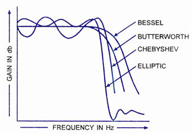
Chebyshev Filter
The Chebyshev active filter is also named as an equal ripple filter. It gives a sharper cutoff than a Butterworth filter in the pass band. Both Chebyshev and Butterworth filters show large phase shifts close to the cutoff frequency. A disadvantage of the Chebyshev filter is the exterior of gain minima and maxima below the cutoff frequency. The adjustable parameter in designing of filter, the gain ripple is expressed in dB.
The implementation of these filters gives a a lot steeper roll- off, but has ripple in the pass-band, so it is not used in audio systems. Though it is far better in some applications where there is only one frequency available in the pass band, but numerous other frequencies are required to eliminate.
Butterworth Active Filter
The Butterworth active filter is also named as flat filter. The implementation of the Butterworth active filter guarantees a flat response in the pass band and an ample roll-off. This group of filters approximates the perfect filter fit in the pass band. Frequency response curves of different kinds of filters are shown. This filter includes an essentially flat amplitude, frequency response up-to the cut¬-off frequency.
The roughness of the cutoff can be seen in the diagram. It is to be famous that all the three filters achieve a roll-off angle of -40db/decade at frequencies much superior than cutoff. This filter has a characteristic somewhere b/n Chebyshev and Bessel filters. It has a sensible roll-off of the skirt &a slightly non¬linear phase responses. This kind of filter is a good, very easy to understand and is excellent for audio processing applications.
Bessel Filter
The Bessel filter gives an ideal phase characteristic with an about linear phase response up to an almost cutoff frequency. Although, it includes a very linear phase response but a quite gentle skirt slope. The applications of this filter involve where the phase characteristic is significant. It is a small phase shift even though its cutoff characteristics are not very intelligent. It is well matched for pulse applications.
The Bessel filter exhibits a stable propagation delay across the i/p frequency spectrum. So applying a square wave to the input of a filter will give a square wave on the o/p with no exceed Further, any filter will wait various frequencies by various amounts. This will evident itself as exceed on the o/p waveform.
Elliptical Filter
The Elliptical Filter is a much more complicated filter like the Chebyshev. It includes a ripple in the pass band & severe roll-off at the cost of ripple in the stop band. This filter has the roll off of every filter in the conversion region, but it has both the regions of stop band and pass band. This filter can be designed to have high attention of particular frequencies in the stop band, which decreases the attenuation of further frequencies in the stop band.
Advantages of Active filters
The advantages of an active filters include the following
- These filters are more reasonable than passive filters.
- The apparatus used in these filters is smaller than the components used in passive filters.
- Active filter doesn’t show any insertion loss.
- It also permits the interstage isolation for controlling of i/p and o/p impedance.
Applications of Active filters
- Active filters are used in communication systems for suppressing noise, to isolate a communication of signal from various channels to improve the unique message signal from a modulated signal.
- These filters are used in instrumentation systems by the designers to choose a required frequency apparatus and detach unwanted ones.
- These filters can be used to limit the analog signal’s bandwidth before altering them to digital signals.
- Analog filters are used in audio systems by engineers to send various frequencies to various speakers. For example, in the music industry, record & playback applications are needed to control the frequency components.
- Active filters are used in biomedical instruments to interface psychological Sensors with diagnostic equipments & data logging.
Currently, numerous types of active filters are at the initial stage due to its short capacity. But, at present many engineers are designing it with large capacities. Effectiveness in the long run will not only pressure consumers with nonlinear load to employ these filters for preserving but also the quality of power at efficient. The configuration of huge number of active filters will be available to reimburse reactive power, harmonic current, unbalanced and neutral current. The customer can choose the active filter with preferred features in the near future as the technology moves on.
Flash Back of Digital filters vs. Analog filters
Digital and analog filters both take out unwanted noise or signal components, but filters work differently in the analog and digital domains. Analog filters will remove everything above or below a chosen cutoff frequency, whereas digital filters can be more precisely programmed. Analog filters that remove signals above a certain frequency are called low pass filters because they let low frequency signals pass through the filter while blocking everything above the cutoff frequency. An analog filter that removes all signals below a certain frequency is a high pass filter, because it lets pass everything higher than the cutoff frequency.

An active high-pass filter.
Analog filters are circuits made of analog components such as resistors, capacitors, inductors, and op amps. Digital filters are often embedded in a chip that operates on digital signals, such as an MCU, SoC, processor, or DSP. Analog filters are fairly simple but increase in complexity if you desire a more precise roll-off; that is, making the filtered result more precisely “step-like” at roll-off requires successively more components.
Digital filters can be more precise in filtering, but the signal must be digital. Placing a digital filter in an analog signal chain would require the analog signal to be converted to a digital signal before the digital filtering could be applied and, with any conversion, there are trade-offs in signal integrity. Digital filters work by oversampling and averaging, and are programmable. But it is wise to apply an analog filter prior to signal conversion so that all unwanted frequencies above or below where the desired signal is reasonably expected to operate are removed first. The conversion process and choosing an analog-to-digital signal converter (ADC) is in itself a careful process that involves choosing a sampling rate that will avoid aliasing during conversion. This is because an aliased signal is indiscernible to a digital filter and therefore the aliased portions of the signal would become a permanent part of the digital signal.
Therefore, choosing an ADC is in itself a task that requires careful attention to Nyquist sampling rates and frequencies. Therefore, although digital filters are more precise and programmable, getting a real world analog signal to an accurate digital representation is half the battle and requires specific knowledge of the expected real-world signal so that specifications for conversion can be defined.
There are shortcuts to the digital domain, however. If you are measuring temperature, for instance, it may be easier to select a digital temperature sensor that does the conversion for you. It’s no surprise, then, that the majority of temperature sensors now available appear to be digital, and thus ready-to-use with an MCU, DSP, SoC, processor or another device that operates in the digital domain.
An Integrated Active Hybrid
Filter for ADSL
System Definitions
• This is a Frequency Division Multiplexed
(FDM) system
•
The Upstream band is defined as data from
the Remote Terminal (RT) to the Central
Office (CO) in frequency range 26kHz –
138kHz
•
The Downstream band is defined as data
from the CO to RT in the frequency range
160kHz –1104kHz
•
The hybrid design presented here is for the
upstream case.
Active Filters Information
Active filters are electronic filers that use active components such as amplifiers. Their output is not attenuated with respect to the input voltage. The amplifier—normally an operational amplifier—provides a feedback mechanism from output to input. This, in turn, provides stability for any signal frequency, and allows for a wider choice of frequency responses and time domain behavior.
Theoretically, any active filter design could be replicated as a passive filter. However, an important advantage in using active filters is that the feedback mechanism provided by the amplifier allows the construction of filters with imaginary poles using only capacitors and resistors. Without feedback, a filter with imaginary poles would need capacitors and inductors. An inductor-free filter is ideal because inductors are prone to pick up unwanted signals due to stray magnetic fields; they are also bulky and expensive. With feedback, smaller capacitor values can be used as well. An active filter often scales down all component values, allowing the production of smaller and less expensive filters.

An active low-pass filter schematic, showing the use of resistors, capacitors, and an amplifier.
However, active filters also have disadvantages when compared to passive designs:
- Capacitor values: Capacitors can be plagued with the same value and spacing issues that affect inductors in passive filters, although to a lesser degree. Standard capacitor values are often widely spaced, making off-the-shelf solutions nearly impossible for applications requiring high accuracy. For designs intended for precise applications, space-constrained environments, or high values, capacitors can be prohibitively expensive.
- Power: Active filters require a power supply to drive amplifier components.
- Noise: Active filters inject noise into the system, although this can be remedied through low-noise amplifiers.
- Frequency range: Active filters have limited bandwidth and are often impractical at high frequencies.
Types
Filters are grouped and specified according to the type of frequencies they suppress or attenuate. The four common filter classifications are listed below.
- Low-pass filters attenuate or suppress signals above a particular cutoff frequency. For example, a low-pass filter (LPF) with a cutoff frequency of 50 Hz can eliminate noise with a frequency of 70 Hz.
- High-pass filters suppress or attenuate signals with frequencies lower than a particular frequency, also called the cutoff or critical frequency. For example, a high-pass filter (HPF) with a cutoff frequency of 100 Hz can be used to suppress the unwanted DC voltage in amplifier systems, if desired.
- Band-pass filters are found in TV and radio circuits. They attenuate or suppress signals with frequencies outside a band of frequencies.
- Band-reject, or notch filters attenuate or suppress signals with a range of frequencies, for example 50-150 Hz.
Response Characteristics
The frequency response of any filter can be designed by properly selecting the circuit components. Filter characteristics are defined by the shape of the frequency response curve, and filters can be classified as:
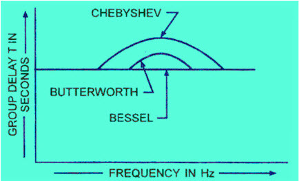
- Bessel filters have a passband that maximizes the group delay at zero frequency, causing a constant group delay in the passband. Group delay is a measurement of the time it takes for a signal to move between two points in a network. A constant group delay in a filter's passband implies that for signals within the passband have an identical time delay. This fact is important in many applications, especially audio, video, and radar applications.
- Butterworth filters are designed so that the frequency response is flat in the passband.
- Chebyshev filters feature a very steep roll-off, but have ripples in the passband.
- Elliptic filters exhibit equalized ripple in both the passband and the stopband.
- Gaussian filters produce no overshoot in response to an input step. They optimize rise and fall times.
- Legendre filters are designed to produce the maximum roll-off rate for a given order and a flat passband frequency response.
IC Electronic Filters Information
Table of Contents
1. Operation
2. Types
Introduction
Electronic filters are electrical circuits designed to remove, attenuate, or alter the characteristics of electrical signals. In particular these devices reduce the magnitude and the phase of unwanted signals with certain frequencies. A common example of an unwanted signal is noise, typically at 60 Hz. Filter operate by passing the system signal (voltage and noise) through a filter. If the filter is designed to suppress or attenuate the magnitude of the noise, its output will contain only (or mostly) the system signal. A typical radio receiver such as a car radio provides another good example. By tuning to a particular station the radio selects a particular signal while attenuating the signals of the other radio stations. This process is accomplished by a filter.
As an example, suppose a signal with frequency f1 is useful for a system, but an undesirable signal (noise) with frequency f2 has mixed with the useful signal, as shown below. Filters are used to suppress the second signal or reduce its amplitude. Part (a) of the figure shows the frequency response of the system, where the unwanted signal is prominent. After passing the signals through a filter designed to attenuate f2, the signal is reduced in amplitude with respect to f1.

Filters are distinguished as analog or digital. Analog filters attenuate signals in analog systems, while digital filters attenuate digital signals in digital systems. This guide pertains to the design of analog filters.
Operation
Suppose a medical technician is measuring a 5 Hz EKG sine wave signal from a patient. The measuring device, however, picks up instrument noise of 50 Hz, so that the actual measured signal is a mix of the noise and desired signal. The two signals must be separated to eliminate the noise. A low-pass filter similar in design to the above diagram is ideal in this situation. The compounded signal is passed through a filter with appropriate design values so that it almost completely attenuates the noise and extracts the EKG signal, as shown below.
The first and second plot of the figure show the original EKG desirable signal and the noise, respectively. The third plot shows the compounded signal, the input signal to the filter circuit. The last plot shows the extracted output signal from the filter. This output is the desired EKG signal. Notice that the peak-to-peak value of the output signal is smaller than the original desirable signal (the first plot in the figure). This is due to the fact that the filter did not completely remove the noise, but this output is reliable enough as to use it as the EKG signal. The output can be improved by selecting better filter parameters.

Types
Filters are broadly classified according to the type of frequencies that the filter is able to suppress or attenuate. In this regard, there are four main categories:
- Low-pass filters attenuate or suppress signals with frequencies above a particular frequency called the cutoff or critical frequency. For example a low-pass filter (LPF) with a cutoff frequency of 40 Hz can eliminate noise with a frequency of 60 Hz.
- High-pass filters suppress or attenuate signals with frequencies lower than a particular frequency, also called the cutoff or critical frequency. For instance a high-pass filter (HPF) with a cutoff frequency of 100 Hz can be used to suppress the unwanted DC voltage in amplifier systems, if desired.
- Band-pass filters attenuate or suppress signals with frequencies outside a band of frequencies. They are commonly seen in TV or radio tuning circuits.
- Band-reject, or notch filters attenuate or suppress signals with a range of frequencies. For instance, a notch filter can be used to reject signals with frequencies between 50 Hz and 150 Hz.
Filter Descriptions
Filters are described using Laplace transforms and frequency-domain tools. In this way their amplitude and phase can be expressed as a function of frequency. The effect of filters on signals is also defined in terms of frequency-domain. A widely used mathematical tool to study filters is a graphical method called frequency response. This is a method used to study the dynamic behavior of systems by looking at the magnitude and phase of the output as a function of frequency. Typically, a filter system is excited with an input signal with a range of frequencies, and its output—magnitude and phase—are plotted as a function of frequency. The figure below shows the frequency response of a band-pass filter. The first graph shows the magnitude of the output as a function of frequency. In this case the magnitude is expressed in decibels (dB), and the frequency axis is a logarithmic axis due to the fact that normally the frequencies represent a large range. The bottom figure shows the phase (in degrees) as a function of frequency.

Ideal Filters
To understand practical, real-world, filters, it is important to understand the behavior (frequency response) of ideal filters. These filters are impossible to build but are good teaching tools. An ideal filter frequency response consists of two or more sections of passband and stopband frequencies. The passband range comprises the frequencies where the response will show an amplitude with a fixed value or gain (normally 1). The stopband range of frequencies are the frequencies where the amplitude is zero. The frequencies at which the response changes from passband to stopband, or vice versa, are called critical frequencies or cutoff frequencies, the transition from stopband to passband and vice versa is instantaneous. The figure below shows the shape of the frequency response for the main four types of filters. Notice that for the bandpass filter (BPF) and the notch or bandstop filter (BS) there are two critical frequencies.

The amplitude is normally the gain of the filter, or the ratio of output voltage and input voltage. In equation form the amplitude is

If the filter circuit contains only passive elements (resistors, capacitors, inductors, etc.) the value of the amplitude for an ideal filter is 1.0, but if the filter is built with active components (transistors, op-amps, etc.) the value of the amplitude (the gain) is different from 1.0. (For more information about passive filters, visit the Passive Filters Specification Guide.)
It is convenient to express the amplitude of the response in decibels (dB). The following equation converts the amplitude from raw numbers (ratio) to decibels.
For passive filters the constant amplitude expressed in dB is zero, or

Practical Filters
It is practically impossible to instantaneously transition from stopband to passband or vice versa, as in the above discussion about ideal filters. Instead of the transition represented by ideal filters, a closer behavior to that of ideal-real filters contains a transition region between the passband and the stopband. There is always a transition range between these two regions, so practical-ideal or real-ideal filters have a frequency response shown in the figure below.

However, this figure still does not represent a practical, real-world filter. The response amplitude passband is typically not a straight, flat horizontal line: it may have attenuation ripples. The transition is not a straight line either. There are oscillations produced by real components that must be taken into account. The stopband may have ripples as well. A more accurate depiction of the frequency response is shown in the low-pass filter response graph below.

As shown in the above graph, there are several parameters in a practical filter:
- Passband: The range of frequencies where the output has a gain.
- Stopband: The range of frequencies where the output is zero or very small.
- Passband ripple: The variations or oscillations in the bandpass, also called error band. In a typical filter, these oscillations occur around the nominal value of 1.0, or at 0 dB, if the amplitude is expresses in decibels. The ripple value is 2a1, where a1 is a parameter dependent on the circuit components.
- Stopband ripple: This represents the variations in the stopband region. The ripple is equal to the parameter a2, which is determined by the values of the circuit components.
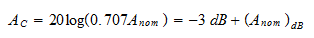
- Critical frequency, fc: This is the frequency at which the response leaves the passband ripple. For certain type of filters (Butterworth filters, for instance), at this frequency the amplitude of the response is
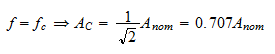
 of the nominal amplitude. If the nominal amplitude is Anomthe value of the amplitude at fc can be determined by using the following equation:
The nominal value in this figure is 1.0, but it can be larger, particularly in active filters.
- Stopband frequency, fs: This is the frequency at which the maximum stopband ripple (a2) occurs.
- Transition band: This represents the range (fs - fc) of frequencies between the critical and cutoff frequencies. The slope or steepness of the transition region is related to the number of poles in the transfer function of the response, also known as the order of the filter. A pole is a root of the denominator of the transfer function. For a standard Butterworth filter every pole adds -20 dB/decade or -6 dB/octave to the slope of the response. The slope of the line is called the roll-off of the transition. Also, a pole represents one RC stage in the circuit, as shown below. A filter that has only one RC network it is called a single-pole or order-one filter; one with two RC circuits is a 2-pole or second order filter, and so on.

Response Characteristics
The frequency response of any filter can be designed by properly selecting the circuit components. Filter characteristics are defined by the shape of the frequency response curve.
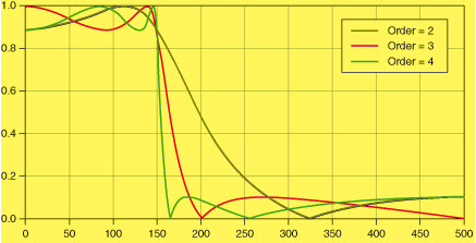
The most important response shapes are named after a researcher who studied the particular filters. These include Butterworth, Chebyshev (types I and II) , elliptic (or Cauer), and Bessel types. Each one of these filter types has a particular advantage in certain applications. The characteristics of four low-pass filters, each one of three-poles and cutoff frequency of 10, is shown below.

Transfer Function
Filters operate on the frequency of signals. Therefore the most powerful tools to describe the behavior of filters are analytical and graphical descriptions using the frequency domain. Thus, frequency domain equations and curves of gain vs. frequency and phase vs. frequency are commonly used. To study the frequency domain of networks their mathematical description in terms of the transfer function of the system is required. For a general system, as depicted below, the voltage transfer function is the ratio of the Laplace transforms of the output and the input signals.
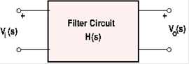
For the system shown above the transfer function is
where Vi(s) and Vo(s) are the input and output voltages and s is the complex Laplace transform variable. In terms of the frequency of the system the Laplace variable is given by

where ω=2πf is the angular frequency in radians per second and σ is the Neper frequency in nepers per second. For casual systems with output dependent on present and past inputs only, σ=0. Therefore s=jω for the filter's characteristics.
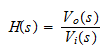
Most electrical systems are frequency-dependent because the impedances of capacitors and inductors are frequency dependent, given by

or, for a capacitor with capacitance C (farads)
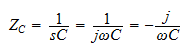
and for an inductor with inductance L (Henry)
Two important sub-equations are derived from the transfer function. The amplitude response represents the magnitude of the complex transfer function as a function of frequency. This describes the effect of the filter on the amplitudes of input signals at various frequencies. The second sub-equation is the phase response of the filter. This equation tells us the amount of phase shift introduced in sinusoidal input signals as a function of frequency. A phase shift of a signal represents a change in time of the output with respect to the input.
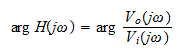
Replacing s with jω in the transfer function equation determines the amplitude and phase response. The amplitude response is the magnitude and is given by
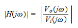
and the phase response is written as
The transfer function of any circuit can be found by using standard network techniques such as Ohm's law, Kirchoff's laws, and superposition. By using complex impedances for capacitors and inductors, the standard form of the transfer function is
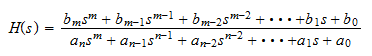
H(s) is a rational function in s and with real coefficients. It is convenient to factor the numerator and denominator polynomials and to write the transfer function accordingly:
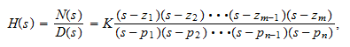
where N(s) and D(s) are the real coefficient numerator and denominator, respectively and K=bm / an. In this equation the zeros (zi) are the roots of

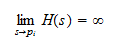
and the poles pi are the roots of the equation

The degree of the numerator is m and the degree of the denominator is n. This equation is expressed such that when s=zi, for i=1...m the numerator becomes

and the transfer function becomes
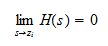
Similarly, when s=pi, for i=1...m the denominator becomes

and
Notice that the coefficients of the numerator and denominator polynomials are real numbers. Therefore the roots must be either real numbers or appear in pairs of complex conjugate numbers. The numerator may be

or
Likewise, for the denominator.
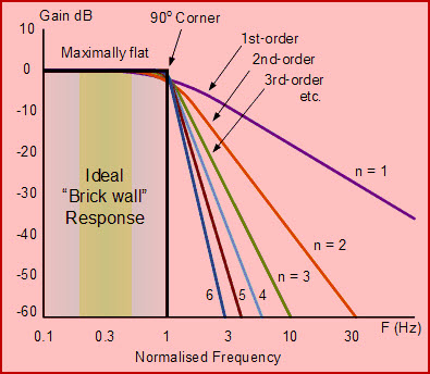
The degree of a filter's denominator is the order of the filter, and the roots of the denominator are the poles of the filter. The roots of the numerators are called the zeros of the filter. Each pole provides -20 dB/decade or -6 dB/octave.
So if a Butterworth filter has 3 poles, and no zeros the slope of the transition band is -60 dB/decade.
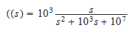
A Practical Example
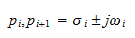
As an example consider the second order low-pass filter with implementation as shown in the following figure.

The transfer function can be found by applying the voltage divider rule across the resistance:
Substituting the values of the circuit, the equation becomes
Factorizing the denominator, it becomes
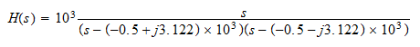
Therefore the filter has a zero at that origin (s=0) and two complex conjugate poles at
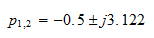
Q & A Active Filter
For successful circuit-building exercises, follow these steps:
- Carefully measure and record all component values prior to circuit construction.
- Draw the schematic diagram for the circuit to be analyzed.
- Carefully build this circuit on a breadboard or other convenient medium.
- Check the accuracy of the circuit’s construction, following each wire to each connection point, and verifying these elements one-by-one on the diagram.
- Mathematically analyze the circuit, solving for all voltage and current values.
- Carefully measure all voltages and currents, to verify the accuracy of your analysis.
- If there are any substantial errors (greater than a few percent), carefully check your circuit’s construction against the diagram, then carefully re-calculate the values and re-measure.
Avoid using the model 741 op-amp, unless you want to challenge your circuit design skills. There are more versatile op-amp models commonly available for the beginner. I recommend the LM324 for DC and low-frequency AC circuits, and the TL082 for AC projects involving audio or higher frequencies.
As usual, avoid very high and very low resistor values, to avoid measurement errors caused by meter “loading”. I recommend resistor values between 1 kΩ and 100 kΩ.
One way you can save time and reduce the possibility of error is to begin with a very simple circuit and incrementally add components to increase its complexity after each analysis, rather than building a whole new circuit for each practice problem. Another time-saving technique is to re-use the same components in a variety of different circuit configurations. This way, you won’t have to measure any component’s value more than once.
Question 2
In very simple, qualitative terms, rate the impedance of capacitors and inductors as “seen” by low-frequency and high-frequency signals alike:
- Capacitor as it “appears” to a low frequency signal: (high or low) impedance?
- Capacitor as it “appears” to a high frequency signal: (high or low) impedance?
- Inductor as it “appears” to a low frequency signal: (high or low) impedance?
- Inductor as it “appears” to a high frequency signal: (high or low) impedance?
Question 3
Draw the Bode plot for an ideal high-pass filter circuit:

Be sure to note the “cutoff frequency” on your plot.
Question 4

Question 5
Identify what type of filter this circuit is, and calculate its cutoff frequency given a resistor value of 1 kΩ and a capacitor value of 0.22 μF:
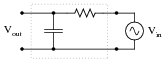
Calculate the impedance of both the resistor and the capacitor at this frequency. What do you notice about these two impedance values?
Question 6
Real filters never exhibit perfect “square-edge” Bode plot responses. A typical low-pass filter circuit, for example, might have a frequency response that looks like this:
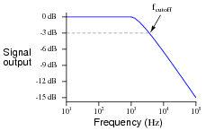
What does the term rolloff refer to, in the context of filter circuits and Bode plots? Why would this parameter be important to a technician or engineer?
Question 7
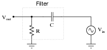
Question 8
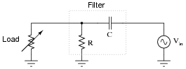
Question 9
In this active filter circuit, how will the filter’s cutoff frequency be affected by changes in the load resistance? Be as specific as you can in your answer.
Question 10
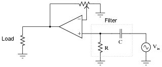


Question 13

Question 14
Describe what will happen to the impedance of both the capacitor and the resistor as the input signal frequency increases:

Also, describe what result the change in impedances will have on the op-amp circuit’s voltage gain. If the input signal amplitude remains constant as frequency increases, what will happen to the amplitude of the output voltage? What type of filtering function does this behavior represent?
Question 15
Describe what will happen to the impedance of both the capacitor and the resistor as the input signal frequency increases:

Also, describe what result the change in impedances will have on the op-amp circuit’s voltage gain. If the input signal amplitude remains constant as frequency increases, what will happen to the amplitude of the output voltage? What type of filtering function does this behavior represent?
Question 16
Approximate the voltage gains of this active filter circuit at f = 0 and f = ∞ (assume ideal op-amp behavior):

Approximate the voltage gains of this other “active filter” circuit at f = 0 and f = ∞ (assume ideal op-amp behavior):
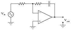
What type of filtering function (low pass, high pass, band pass, band stop) is provided by both these filter circuits? Comparing these two circuit designs, which one do you think is more practical? Explain your answer.
Question 17
Approximate the voltage gains of this active filter circuit at f = 0 and f = ∞ (assume ideal op-amp behavior):

Approximate the voltage gains of this other “active filter” circuit at f = 0 and f = ∞ (assume ideal op-amp behavior):

What type of filtering function (low pass, high pass, band pass, band stop) is provided by both these filter circuits? Comparing these two circuit designs, which one do you think is more practical? Explain your answer.
Question 18
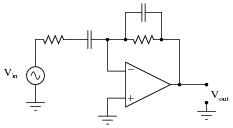
Question 19
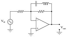
Question 20


Question 21
Question 22
Choose appropriate values for this Sallen-Key high-pass filter circuit to give it a cutoff frequency of 7 kHz with a “Butterworth” response:

|
A good guideline to follow is to make sure no component impedance (ZR or ZC) at the cutoff frequency is less than 1 kΩ or greater than 100 kΩ.
Question 23
Choose appropriate values for this Sallen-Key low-pass filter circuit to give it a cutoff frequency of 4.2 kHz with a “Butterworth” response:
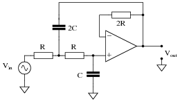
|
A good guideline to follow is to make sure no component impedance (ZR or ZC) at the cutoff frequency is less than 1 kΩ or greater than 100 kΩ.
Question 24
A popular passive filtering network called the twin-tee is often coupled with an operational amplifier to produce an active filter circuit. Two examples are shown here:
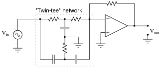
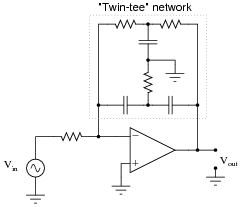
Identify which of these circuits is band-pass, and which is band-stop. Also, identify the type of response typically provided by the twin-tee network alone, and how that response is exploited to make two different types of active filter responses.
Question 25
Singers who wish to practice singing to popular music find that the following vocal eliminator circuit is useful:

The circuit works on the principle that vocal tracks are usually recorded through a single microphone at the recording studio, and thus are represented equally on each channel of a stereo sound system. This circuit effectively eliminates the vocal track from the song, leaving only the music to be heard through the headphone or speaker.
Operational amplifiers U1 and U2 provide input buffering so that the other opamp circuits do not excessively load the left and right channel input signals. Opamp U3 performs the subtraction function necessary to eliminate the vocal track.
You might think that these three opamps would be sufficient to make a vocal eliminator circuit, but there is one more necessary feature. Not only is the vocal track common to both left and right channels, but so is most of the bass (low-frequency) tones. Thus, the first three opamps (U1, U2, and U3) eliminate both vocal and bass signals from getting to the output, which is not what we want.
Explain how the other three opamps (U4, U5, and U6) work to restore bass tones to the output so they are not lost along with the vocal track.
Question 26
Predict how the operation of this active filter circuit will be affected as a result of the following faults. Consider each fault independently (i.e. one at a time, no multiple faults):

- Resistor R1 fails open:
- Capacitor C1 fails open:
- Solder bridge (short) across resistor R1:
- Solder bridge (short) across capacitor C1:
- Resistor R2 fails open:
- Resistor R3 fails open:
For each of these conditions, explain why the resulting effects will occur.
Question 27
Predict how the operation of this active filter circuit will be affected as a result of the following faults. Consider each fault independently (i.e. one at a time, no multiple faults):
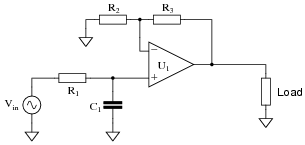
- Resistor R1 fails open:
- Capacitor C1 fails open:
- Solder bridge (short) across resistor R1:
- Solder bridge (short) across capacitor C1:
- Resistor R2 fails open:
- Resistor R3 fails open:
For each of these conditions, explain why the resulting effects will occur.
Question 28
Predict how the operation of this active differentiator circuit will be affected as a result of the following faults. Consider each fault independently (i.e. one at a time, no multiple faults):

- Resistor R1 fails open:
- Capacitor C1 fails open:
- Solder bridge (short) across resistor R1:
- Solder bridge (short) across capacitor C1:
For each of these conditions, explain why the resulting effects will occur.
Question 29
Predict how the operation of this active filter circuit will be affected as a result of the following faults. Consider each fault independently (i.e. one at a time, no multiple faults):

- Resistor R1 fails open:
- Resistor R2 fails open:
- Capacitor C1 fails open:
- Solder bridge (short) across resistor R1:
- Solder bridge (short) across resistor R2:
- Solder bridge (short) across capacitor C1:
For each of these conditions, explain why the resulting effects will occur.
Question 30
Predict how the operation of this active filter circuit will be affected as a result of the following faults. Consider each fault independently (i.e. one at a time, no multiple faults):

- Resistor R1 fails open:
- Resistor R2 fails open:
- Capacitor C1 fails open:
- Solder bridge (short) across resistor R1:
- Solder bridge (short) across resistor R2:
- Solder bridge (short) across capacitor C1:
For each of these conditions, explain why the resulting effects will occur.
Question 31
This vocal eliminator circuit used to work just fine, but then one day it seemed to lose a lot of its bass. It still did its job of eliminating the vocal track, but instead of hearing the full range of musical tones it only reproduced the high frequencies, while the low frequency tones were lost:
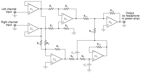
Identify the following fault possibilities:
One resistor failure (either open or shorted) that could cause this to happen:
One capacitor failure (either open or shorted) that could cause this to happen:
One opamp failure that could cause this to happen:
For each of these proposed faults, explain why the bass tones would be lost.
Question 32
This vocal eliminator circuit used to work just fine, but then one day it stopped eliminating the vocal track. The tone of the music sounded a bit heavy on the bass, and the vocal track was there when it shouldn’t have been there:

Identify the following fault possibilities:
One resistor failure (either open or shorted) that could cause this to happen:
One opamp failure that could cause this to happen:
For each of these proposed faults, explain why the bass tones would be lost.
Analogies of filters
- Everyone would have experienced the noise while talking over phones, at least once. Most often, we would say to the person on the other side as, “I am not able to hear you properly. There is lots of noise in your network”. In serving this purpose, the phones will have micro filters installed in them to remove the noise.
- When music is played in one room, and if you are in the room nearby, you can hear only the lowest notes of the music and you cannot hear the high frequency notes, in the nearby room. Here, the walls of the room act as a low pass filter. It passes only the low frequency notes of the music and the high frequency music will not be passed through.
What is a filter?
A filter is a frequency selective circuit that allows only a certain band of the desired frequency components of an input signal to pass through, and attenuates the signals of undesired frequency components.
Why filters are used in electronic circuits?
In electronic circuits, noise is a major source of interference with the desired signal. Any unwanted signal associated with the desired signal is noise. In any electronic system, noise can come from external sources as well as be self-induced, as a result of the circuitry itself.
Examples of external noise sources are switching or rotating machinery, ignition systems, and control circuits. Natural phenomena such as lightning may also be an external noise source.
The internal noise may be caused by the ac random voltages and currents, generated within the conductors and semiconductors of one circuit as a result of switching of another circuit. The rate of change of current and voltage per unit of time, the speed of operation of the circuit, and the type of coupling between two circuits are some of the factors that determine the amount of noise induced in a given circuit.
To remove these associated noises in the circuits, filters are used. Depending on the application, the filters are widely grouped as analog and digital filters.
It is sometimes desirable to have circuits capable of selectively filtering one frequency or range of frequencies out of a mix of different frequencies in a circuit. A circuit designed to perform this frequency selection is called a filter circuit, or simply a filter. A common need for filter circuits is in high-performance stereo systems, where certain ranges of audio frequencies need to be amplified or suppressed for best sound quality and power efficiency. You may be familiar with equalizers, which allow the amplitudes of several frequency ranges to be adjusted to suit the listener's taste and acoustic properties of the listening area. You may also be familiar with crossover networks, which block certain ranges of frequencies from reaching speakers. A tweeter (high-frequency speaker) is inefficient at reproducing low-frequency signals such as drum beats, so a crossover circuit is connected between the tweeter and the stereo's output terminals to block low-frequency signals, only passing high-frequency signals to the speaker's connection terminals. This gives better audio system efficiency and thus better performance. Both equalizers and crossover networks are examples of filters, designed to accomplish filtering of certain frequencies.
Another practical application of filter circuits is in the “conditioning” of non-sinusoidal voltage wave forms in power circuits. Some electronic devices are sensitive to the presence of harmonics in the power supply voltage, and so require power conditioning for proper operation. If a distorted sine-wave voltage behaves like a series of harmonic waveforms added to the fundamental frequency, then it should be possible to construct a filter circuit that only allows the fundamental waveform frequency to pass through, blocking all (higher-frequency) harmonics.
Another practical application of filter circuits is in the “conditioning” of non-sinusoidal voltage wave forms in power circuits. Some electronic devices are sensitive to the presence of harmonics in the power supply voltage, and so require power conditioning for proper operation. If a distorted sine-wave voltage behaves like a series of harmonic waveforms added to the fundamental frequency, then it should be possible to construct a filter circuit that only allows the fundamental waveform frequency to pass through, blocking all (higher-frequency) harmonics.
+++++++++++++++++++++++++++++++++++++++++++++++++++++++++++++++
e- Signal Purification to e- Filtering Perform

+++++++++++++++++++++++++++++++++++++++++++++++++++++++++++++++
Tidak ada komentar:
Posting Komentar