


The electronics industry is filled with an electronic circuit in the field of control and measurement which is an important aspect for the performance of an electronic circuit, especially in the WET ON / OFF Automatic grid process (Work ---> Energy ---> Time ON / OFF Automatic). all areas of life at this time can come into contact with the performance of electronic equipment for it required a work WET ON / OFF Automatic highly efficient and effective as well as the right quality and the right quantity in which the electronic equipment is needed for the journey journey distant and excavation extracting information qualified in the field of outer space ie engineering machinery electronic and control Avionics ( Space Ships ) and acquisition techniques of quality information both mixed and determine which ones are valuable and useful ( INFORMIX ) , or could we call detector information from technical space, a glimpse here I outline some of the principles of electronics WET ON / OFF Automatic in the field of modern electronics .
Electronic Components
 Electronic components are used in the automotive, communication, aerospace and other industries. Miniaturization, higher package density and accelerated development processes have a great impact on the reliability of electronic components.
Rapid changes of ambient temperature or internal production of heat may occur during operation. This may create high thermal stresses due to the mismatch of the thermal expansion coefficients of the different materials in electronic components.
Shrinking dimensions of flip chip assemblies make inspection of bumps or solder joints always more difficult as standard non destructive control techniques reach their resolution limits.
Electronic speckle pattern interferometry (ESPI) as a non-contact, full-field and 3-dimensional measuring method, copes well with the challenge of deformation measurements on microsystems and electronic components with a sub-micron resolution.
The Basics of Mixers
The Basics of Mixers
Contributed By Electronic Products
2011-10-20
Mixers are used in a variety of RF/microwave applications, including military radar, cellular base stations, and more. An RF mixer is a three-port passive or active device that can modulate or demodulate a signal. The purpose is to change the frequency of an electromagnetic signal while (hopefully) preserving every other characteristic (such as phase and amplitude) of the initial signal. A principal reason for frequency conversion is to allow amplification of the received signal at a frequency other than that of the RF.

Figure 1: A mixer presented symbolically.
Figure 1 shows the mixer’s three ports: fin1 and fin2 are the input ports while the output port is the both the sum and the difference in frequency of the inputs:
fout = fin1 ± fin2

Figure 2: Representation of downconversion and upconversion.
The three ports (Figure 2) are referred to as the RF input port, LO (local oscillator) input port, and the IF (intermediate frequency) output port. A mixer is also known as a downconverter if the mixer is part of a receiver or as an upconverter if it is part of a transmitter.
Depending upon the application in which the mixer is being used, the LO is typically driven with either a sinusoidal continuous wave signal or a square wave. In concept, the LO signal acts as a gate of the mixer in which the mixer is considered ON when the LO is a large voltage and OFF when it is a small voltage. The LO can only be an input port, while the RF and IF ports can be interchanged between the second input or output.
When the desired frequency is less than the second input frequency, the process is called downconversion. The RF is then the input while the IF is the output. When the desired output frequency is greater than the second input frequency the process is called upconversion. Here the IF is the input while the RF is the output.
In a receiver, when the LO frequency is less than the RF frequency, it is called low-side injection and the mixer is a low-side downconverter. When the LO frequency is above the RF, it is called high-side injection, and the mixer is a high-side downconverter.
Generally, a passive mixer is made of passive devices, such as diodes. An active mixer is made of active devices, such as transistors. Active or passive implementations are used depending on the application, and there are advantages and disadvantages. As an example, a passive implementation that uses diodes as nonlinear elements or FETs as passive switches, exhibits a conversion loss rather than gain. This may impact the overall noise performance of the system, so in this case an LNA is usually added prior to the mixer.
Passive mixers are widely used due to their simplicity, wide bandwidth, and good intermodulation distortion (IMD) performance. Active mixers are mostly used for RFIC implementation. They are configured to provide conversion gain, good isolation between the signal ports, and require less power to drive the LO port. They can be monolithically integrated with other signal processing circuitry and are less sensitive to load-matching.
There are three basic types of active and passive mixers: unbalanced, single-balanced, and double-balanced.
Some mixer parameters that engineers will find in a datasheet are as follows:
- Conversion loss or gain: Measured in dB, conversion gain measures the signal gain in an active mixer, while conversion loss (known also as CL) measures the insertion loss in a passive mixer. Conversion gain is defined as the ratio of the IF output power to the RF input power. For passive mixers, CL is the most important parameter next to the noise figure. It is defined as the difference in power between the input RF power level and the desired output IF frequency power level. Of course, the lower the CL the better. Typical values of conversion loss range between 4.5 to 9 dB. Other losses that may occur are from transmission line losses, balun mismatch, diode series resistance, and mixer imbalance. In addition, the wider the frequency ranges for the three ports, the worse the CL.
- Input intercept point (IIP3): IIP3 is the RF input power at which the output power of the unwanted intermodulation products and the desired IF output would be equal.
- Spurious: Spurious external signals generate undesired frequencies that may fall into the IF-band. Spur tables provided by manufacturers show the relative amplitudes of each response under given LO drive conditions
- Isolation: This is defined as the amount of power leakage from one port to another. When isolation is high, the leakage between the ports will be small.
- Noise figure (NF): Defined as the added noise generated by the mixer and present at the IF output, the noise figure is the second important parameter (CL is the first) for the passive filter. For a passive mixer, the NF is almost equal to the loss.
- Dynamic range: This is the signal power range over which a mixer provides useful operation.
Selecting a mixer
Mixer selection depends on many factors and, most of all, on the requirements of an application. Determine the LO, RF, and IF frequency ranges involved as well as the LO drive required. Some applications require a specific amount of harmonic distortion. Finally, determine the type of packaging the mixer will have.
A wide selection of mixers can be found on the Digi-Key site. Below are a few examples.

Figure 3: Linear Technology LT5560.
Linear Technology offers the LT5560, a low-power high-performance broadband active mixer. This double-balanced mixer can be driven by a single-ended LO source and requires only –2 dBm of LO power. The balanced design results in low LO leakage to the output, while the integrated input amplifier provides excellent LO-to-IN isolation. The signal ports can be impedance-matched to a broad range of frequencies, which allows the LT5560 to be used as an upconversion or downconversion mixer in a wide variety of applications.

Figure 4: Maxim’s MAX2682 circuit.
The MAX2680/MAX2681/MAX2682 from Maxim Integrated Products are small, low-cost, low-noise downconverting mixers designed for low voltage operation and well-suited for use in portable communications equipment. Signals at the RF input port are mixed with signals at the LO port using a double-balanced mixer. These downconverter mixers operate with RF input frequencies between 400 MHz and 2,500 MHz, and downconvert to IF output frequencies between 10 and 500 MHz.
NXP Semiconductor offers the BGA2022 MMIC mixer that features a wide frequency range: Cellular band (900 MHz), PCS band (1,900 MHz), and WLAN band (2.4 GHz). Specifications (with reference to VS = 2.8 V; IS = 6 mA; PLO = 0 dBm; fRF = 1,800 MHz; fLO = 2080 MHz; fIF = 280MHz) include a high conversion gain of 6 dB typical, a noise figure (DSB) of 12 dB typical, and an output third order intercept point of 7 dBm.
Summary
The purpose of the mixer is to provide both the sum and difference frequency at the output port when two input frequencies are provided at the other two ports. The designer should fully understand all mixer properties to efficiently translate this frequency properly and without any distortions.
Frequency mixer
In electronics, a mixer, or frequency mixer, is a nonlinear electrical circuit that creates new frequencies from two signals applied to it. In its most common application, two signals are applied to a mixer, and it produces new signals at the sum and difference of the original frequencies. Other frequency components may also be produced in a practical frequency mixer.
Mixers are widely used to shift signals from one frequency range to another, a process known as heterodyning, for convenience in transmission or further signal processing. For example, a key component of a superheterodyne receiver is a mixer used to move received signals to a common intermediate frequency. Frequency mixers are also used to modulate a carrier signal in radio transmitters.

Frequency mixer symbol
Types
The essential characteristic of a mixer is that it produces a component in its output which is the product of the two input signals. A device that has a non-linear (e.g. exponential) characteristic can act as a mixer. Passive mixers use one or more diodes and rely on their non-linear relation between voltage and current to provide the multiplying element. In a passive mixer, the desired output signal is always of lower power than the input signals.
Active mixers use an amplifying device (such as a transistor or vacuum tube) to increase the strength of the product signal. Active mixers improve isolation between the ports, but may have higher noise and more power consumption. An active mixer can be less tolerant of overload.
Mixers may be built of discrete components, may be part of integrated circuits, or can be delivered as hybrid modules.

Mixers may also be classified by their topology:
- An unbalanced mixer, in addition to producing a product signal, allows both input signals to pass through and appear as components in the output.
- A single balanced mixer is arranged with one of its inputs applied to a balanced (differential) circuit so that either the local oscillator (LO) or signal input (RF) is suppressed at the output, but not both.
- A double balanced mixer has both its inputs applied to differential circuits, so that neither of the input signals and only the product signal appears at the output.[1] Double balanced mixers are more complex and require higher drive levels than unbalanced and single balanced designs.
Selection of a mixer type is a trade off for a particular application.
Mixer circuits are characterized by their properties such as conversion gain (or loss), and noise figure.
Nonlinear electronic components that are used as mixers include diodes, transistors biased near cutoff, and at lower frequencies, analog multipliers. Ferromagnetic-core inductors driven into saturation have also been used. In nonlinear optics, crystals with nonlinear characteristics are used to mix two frequencies of laser light to create optical heterodynes.
Diode
A diode can be used to create a simple unbalanced mixer. This type of mixer produces the original frequencies as well as their sum and their difference. The significant property of the diode here is its non-linearity (or non-Ohmic behavior), which means its response (current) is not proportional to its input (voltage). The diode does not reproduce the frequencies of its driving voltage in the current through it, which allows the desired frequency manipulation. The current I through an ideal diode as a function of the voltage V across it is given by

where what is important is that V appears in e's exponent. The exponential can be expanded as

and can be approximated for small x (that is, small voltages) by the first few terms of that series:

Suppose that the sum of the two input signals is applied to a diode, and that an output voltage is generated that is proportional to the current through the diode (perhaps by providing the voltage that is present across a resistor in series with the diode). Then, disregarding the constants in the diode equation, the output voltage will have the form


The first term on the right is the original two signals, as expected, followed by the square of the sum, which can be rewritten as , where the multiplied signal is obvious. The ellipsis represents all the higher powers of the sum which we assume to be negligible for small signals.

Suppose that two input sinusoids of different frequencies are fed into the diode, such that and . The signal becomes:


Expanding the square term yields:

Ignoring all terms except for the term and utilizing the prosthaphaeresis (product to sum) identity,


yields,

demonstrating how new frequencies are created from the mixer.
Switching
Another form of mixer operates by switching, with the smaller input signal being passed inverted or non inverted according to the phase of the local oscillator (LO). This would be typical of the normal operating mode of a packaged double balanced mixer, with the local oscillator drive considerably higher than the signal amplitude.
The aim of a switching mixer is to achieve linear operation over the signal level by means of hard switching driven by the local oscillator. Mathematically the switching mixer is not much different from a multiplying mixer, just because instead of the LO sine wave term we would use the signum function. In the frequency domain the switching mixer operation leads to the usual sum and difference frequencies, but also to further terms e.g. ±3fLO, ±5fLO, etc. The advantage of a switching mixer is that it can achieve (with the same effort) a lower noise figure (NF) and larger conversion gain. This is because the switching diodes or transistors act either like a small resistor (switch closed) or large resistor (switch open), and in both cases only a minimal noise is added. From the circuit perspective, many multiplying mixers can be used as switching mixers, just by increasing the LO amplitude. So RF engineers simply talk about mixers and mean switching mixers.
The mixer circuit can be used not only to shift the frequency of an input signal as in a receiver, but also as a product detector, modulator, phase detector or frequency multiplier. For example, a communications receiver might contain two mixer stages for conversion of the input signal to an intermediate frequency and another mixer employed as a detector for demodulation of the signal.
Product detector
A product detector is a type of demodulator used for AM and SSB signals. Rather than converting the envelope of the signal into the decoded waveform like an envelope detector, the product detector takes the product of the modulated signal and a local oscillator, hence the name. A product detector is a frequency mixer.
Product detectors can be designed to accept either IF or RF frequency inputs. A product detector which accepts an IF signal would be used as a demodulator block in a superheterodyne receiver, and a detector designed for RF can be combined with an RF amplifier and a low-pass filter into a direct-conversion receiver.
A simple product detector
The simplest form of product detector mixes (or heterodynes) the RF or IF signal with a locally derived carrier (the Beat Frequency Oscillator, or BFO) to produce an audio frequency copy of the original audio signal and a mixer product at twice the original RF or IF frequency. This high-frequency component can then be filtered out, leaving the original audio frequency signal.
Mathematical model of the simple product detector
If m(t) is the original message, the AM signal can be shown to be

Multiplying the AM signal x(t) by an oscillator at the same frequency as and in phase with the carrier yields

which can be re-written as

After filtering out the high-frequency component based around cos(2ωt) and the DC component C, the original message will be recovered.
Drawbacks of the simple product detector
Although this simple detector works, it has two major drawbacks:
- The frequency of the local oscillator must be the same as the frequency of the carrier, or else the output message will fade in and out in the case of AM, or be frequency shifted in the case of SSB
- Once the frequency is matched, the phase of carrier must be obtained, or else the demodulated message will be attenuated, but the noise will not be.
Frequency of an AM carrier can be accurately determined with a phase-locked loop, but for SSB, the only solution is to construct a highly stable oscillator.
Another example
There are many other kinds of product detectors as well, which are practical if one has access to digital signal processing equipment. For instance, it is possible to multiply the incoming signal by the carrier, times the square of another carrier 90° out of phase with it. This will produce a copy of the original message, and another AM signal at the fourth harmonic, by means of the trigonometric identity

The high-frequency component can again be filtered out, leaving the original signal.
Mathematical model of the detector
If m(t) is the original message, the AM signal can be shown to be
Multiplying the AM signal by the new set of frequencies yields


After filtering out the component based around cos(4ωt) and the DC component C, the original message will be recovered.
A more sophisticated product detector
A more sophisticated product detector can be constructed in a way much like a single-sideband modulator. Two copies of the modulated input signals are created. The first copy is mixed with a local oscillator and low-pass filtered. The second copy is mixed with a 90° phase-shifted copy of the oscillator and the output of this mixer is also 90° phase-shifted and then low-pass filtered. These copies are then combined to produce the original message. This operation is similar to that performed by a dual-phase lock-in amplifier. Example: I-Q Demodulator
Advantages and disadvantages
The product demodulator has some advantages over an envelope detector for AM signal reception.
- The product demodulator can decode overmodulated AM and AM with suppressed carrier.
- A signal demodulated with a product detector will have a higher signal to noise ratio than the same signal demodulated with an envelope detector.
On the other hand, the envelope detector is a simple and relatively inexpensive circuit, and it can provide higher fidelity, since there is no possibility of mistuning the local oscillator.
A product detector (or equivalent) is needed to demodulate SSB signals.
Optical heterodyne detection
Optical heterodyne detection is a method of extracting information encoded as modulation of the phase and/or frequency (wavelength) of electromagnetic radiation in the wavelength band of visible or infrared light. The light signal is compared with standard or reference light from a "local oscillator" (LO) that would have a fixed offset in frequency and phase from the signal if the latter carried null information. "Heterodyne" signifies more than one frequency, in contrast to the single frequency employed in homodyne detection.
The comparison of the two light signals is typically accomplished by combining them in a photodiode detector, which has a response that is linear in energy, and hence quadratic in amplitude of electromagnetic field. Typically, the two light frequencies are similar enough that their difference or beat frequency produced by the detector is in the radio or microwave band that can be conveniently processed by electronic means.
This technique became widely applicable to topographical and velocity-sensitive imaging with the invention in the 1990s of synthetic array heterodyne detection. The light reflected from a target scene is focussed on a relatively inexpensive photodetector consisting of a single large physical pixel, while a different LO frequency is also tightly focussed on each virtual pixel of this detector, resulting in an electrical signal from the detector carrying a mixture of beat frequencies that can be electronically isolated and distributed spatially to present an image of the scene.
Optical heterodyne detection began to be studied at least as early as 1962, within two years of the construction of the first laser.[3]
Contrast to conventional radio frequency (RF) heterodyne detection
It is instructive to contrast the practical aspects of optical band detection to Radio Frequency (RF) band heterodyne detection.
Energy versus electric field detection
Unlike RF band detection, optical frequencies oscillate too rapidly to directly measure and process the electric field electronically. Instead optical photons are (usually) detected by absorbing the photon's energy, thus only revealing the magnitude, and not by following the electric field phase. Hence the primary purpose of heterodyne mixing is to down shift the signal from the optical band to an electronically tractable frequency range.
In RF band detection, typically, the electromagnetic field drives oscillatory motion of electrons in an antenna; the captured EMF is subsequently electronically mixed with a local oscillator (LO) by any convenient non-linear circuit element with a quadratic term (most commonly a rectifier). In optical detection, the desired non-linearity is inherent in the photon absorption process itself. Conventional light detectors—so called "Square-law detectors"—respond to the photon energy to free bound electrons, and since the energy flux scales as the square of the electric field, so does the rate at which electrons are freed. A difference frequency only appears in the detector output current when both the LO and signal illuminate the detector at the same time, causing the square of their combined fields to have a cross term or "difference" frequency modulating the average rate at which free electrons are generated.
Wideband local oscillators for coherent detection
Another point of contrast is the expected bandwidth of the signal and local oscillator. Typically, an RF local oscillator is a pure frequency; pragmatically, "purity" means that a local oscillator's frequency bandwidth is much much less than the difference frequency. With optical signals, even with a laser, it is not simple to produce a reference frequency sufficiently pure to have either an instantaneous bandwidth or long term temporal stability that is less than a typical megahertz or kilohertz scale difference frequency. For this reason, the same source is often used to produce the LO and the signal so that their difference frequency can be kept constant even if the center frequency wanders.
As a result, the mathematics of squaring the sum of two pure tones, normally invoked to explain RF heterodyne detection, is an oversimplified model of optical heterodyne detection. Nevertheless, the intuitive pure-frequency heterodyne concept still holds perfectly for the wideband case provided that the signal and LO are mutually coherent. Indeed, one can obtain narrow-band interference from coherent broadband sources: this is the basis for white light interferometry and optical coherence tomography. Mutual coherence permits the rainbow in Newton's rings, and supernumerary rainbows.
Consequently, optical heterodyne detection is usually performed as interferometry where the LO and signal share a common origin, rather than, as in radio, a transmitter sending to a remote receiver. The remote receiver geometry is uncommon because generating a local oscillator signal that is coherent with a signal of independent origin is technologically difficult at optical frequencies. However, lasers of sufficiently narrow linewidth to allow the signal and LO to originate from different lasers do exist.[4]
Photon Counting
After optical heterodyne became an established technique, consideration was given to the conceptual basis for operation at such low signal light levels that "only a few, or even fractions of, photons enter the receiver in a characteristic time interval".[5] It was concluded that even when photons of different energies are absorbed at a countable rate by a detector at different (random) times, the detector can still produce a difference frequency. Hence light seems to have wave-like properties not only as it propagates through space, but also when it interacts with matter.[6] Progress with photon counting was such that by 2008 it was proposed that, even with larger signal strengths available, it could be advantageous to employ local oscillator power low enough to allow detection of the beat signal by photon counting. This was understood to have a main advantage of imaging with available and rapidly developing large-format multi-pixel counting photodetectors.
Photon counting was applied with frequency-modulated continuous wave (FMCW) lasers. Numerical algorithms were developed to optimize the statistical performance of the analysis of the data from photon counting.
Key benefits
Gain in the detection
The amplitude of the down-mixed difference frequency can be larger than the amplitude of the original signal itself. The difference frequency signal is proportional to the product of the amplitudes of the LO and signal electric fields. Thus the larger the LO amplitude, the larger the difference-frequency amplitude. Hence there is gain in the photon conversion process itself.
![{\displaystyle I\propto \left[E_{\mathrm {sig} }\cos(\omega _{\mathrm {sig} }t+\varphi )+E_{\mathrm {LO} }\cos(\omega _{\mathrm {LO} }t)\right]^{2}\propto {\frac {1}{2}}E_{\mathrm {sig} }^{2}+{\frac {1}{2}}E_{\mathrm {LO} }^{2}+2E_{\mathrm {LO} }E_{\mathrm {sig} }\cos(\omega _{\mathrm {sig} }t+\varphi )\cos(\omega _{\mathrm {LO} }t)}](https://wikimedia.org/api/rest_v1/media/math/render/svg/7b8b4a38cfd681f8581692c522554320e006858e)
The first two terms are proportional to the average (DC) energy flux absorbed (or, equivalently, the average current in the case of photon counting). The third term is time varying and creates the sum and difference frequencies. In the optical regime the sum frequency will be too high to pass through the subsequent electronics. In many applications the signal is weaker than the LO, thus it can be seen that gain occurs because the energy flux in the difference frequency is greater than the DC energy flux of the signal by itself .


Preservation of optical phase
By itself, the signal beam's energy flux, , is DC and thus erases the phase associated with its optical frequency; Heterodyne detection allows this phase to be detected. If the optical phase of the signal beam shifts by an angle phi, then the phase of the electronic difference frequency shifts by exactly the same angle phi. More properly, to discuss an optical phase shift one needs to have a common time base reference. Typically the signal beam is derived from the same laser as the LO but shifted by some modulator in frequency. In other cases, the frequency shift may arise from reflection from a moving object. As long as the modulation source maintains a constant offset phase between the LO and signal source, any added optical phase shifts over time arising from external modification of the return signal are added to the phase of the difference frequency and thus are measurable.
Mapping optical frequencies to electronic frequencies allows sensitive measurements
As noted above, the difference frequency linewidth can be much smaller than the optical linewidth of the signal and LO signal, provided the two are mutually coherent. Thus small shifts in optical signal center-frequency can be measured: For example, Doppler lidar systems can discriminate wind velocities with a resolution better than 1 meter per second, which is less than a part in a billion Doppler shift in the optical frequency. Likewise small coherent phase shifts can be measured even for nominally incoherent broadband light, allowing optical coherence tomography to image micrometer-sized features. Because of this, an electronic filter can define an effective optical frequency bandpass that is narrower than any realizable wavelength filter operating on the light itself, and thereby enable background light rejection and hence the detection of weak signals.
Noise reduction to shot noise limit
As with any small signal amplification, it is most desirable to get gain as close as possible to the initial point of the signal interception: moving the gain ahead of any signal processing reduces the additive contributions of effects like resistor Johnson-Nyquist noise, or electrical noises in active circuits. In optical heterodyne detection, the mixing-gain happens directly in the physics of the initial photon absorption event, making this ideal. Additionally, to a first approximation, absorption is perfectly quadratic, in contrast to RF detection by a diode non-linearity.
One of the virtues of heterodyne detection is that the difference frequency is generally far removed spectrally from the potential noises radiated during the process of generating either the signal or the LO signal, thus the spectral region near the difference frequency may be relatively quiet. Hence, narrow electronic filtering near the difference frequency is highly effective at removing the remaining, generally broadband, noise sources.
The primary remaining source of noise is photon shot noise from the nominally constant DC level, which is typically dominated by the Local Oscillator (LO). Since the Shot noise scales as the amplitude of the LO electric field level, and the heterodyne gain also scales the same way, the ratio of the shot noise to the mixed signal is constant no matter how large the LO.
Thus in practice one increases the LO level, until the gain on the signal raises it above all other additive noise sources, leaving only the shot noise. In this limit, the signal to noise ratio is affected by the shot noise of the signal only (i.e. there is no noise contribution from the powerful LO because it divided out of the ratio). At that point there is no change in the signal to noise as the gain is raised further. (Of course, this is a highly idealized description; practical limits on the LO intensity matter in real detectors and an impure LO might carry some noise at the difference frequency)
Key problems and their solutions
Array detection and imaging
Array detection of light, i.e. detecting light in a large number of independent detector pixels, is common in digital camera image sensors. However, it tends to be quite difficult in heterodyne detection, since the signal of interest is oscillating (also called AC by analogy to circuits), often at millions of cycles per second or more. At the typical frame rates for image sensors, which are much slower, each pixel would integrate the total light received over many oscillation cycles, and this time-integration would destroy the signal of interest. Thus a heterodyne array must usually have parallel direct connections from every sensor pixel to separate electrical amplifiers, filters, and processing systems. This makes large, general purpose, heterodyne imaging systems prohibitively expensive. For example, simply attaching 1 million leads to a megapixel coherent array is a daunting challenge.
To solve this problem, synthetic array heterodyne detection (SAHD) was developed.[2] In SAHD, large imaging arrays can be multiplexed into virtual pixels on a single element detector with single readout lead, single electrical filter, and single recording system. The time domain conjugate of this approach is Fourier transform heterodyne detection,[11] which also has the multiplex advantage and also allows a single element detector to act like an imaging array. SAHD has been implemented as Rainbow heterodyne detection[12][13]in which instead of a single frequency LO, many narrowly spaced frequencies are spread out across the detector element surface like a rainbow. The physical position where each photon arrived is encoded in the resulting difference frequency itself, making a virtual 1D array on a single element detector. If the frequency comb is evenly spaced then, conveniently, the Fourier transform of the output waveform is the image itself. Arrays in 2D can be created as well, and since the arrays are virtual, the number of pixels, their size, and their individual gains can be adapted dynamically. The multiplex disadvantage is that the shot noise from all the pixels combine since they are not physically separated.
Speckle and diversity reception
As discussed, the LO and signal must be temporally coherent. They also need to be spatially coherent across the face of the detector or they will destructively interfere. In many usage scenarios the signal is reflected from optically rough surfaces or passes through optically turbulent media leading to wavefronts that are spatially incoherent. In laser scattering this is known as speckle.
In RF detection the antenna is rarely larger than the wavelength so all excited electrons move coherently within the antenna, whereas in optics the detector is usually much larger than the wavelength and thus can intercept a distorted phase front, resulting in destructive interference by out-of-phase photo-generated electrons within the detector.
While destructive interference dramatically reduces the signal level, the summed amplitude of a spatially incoherent mixture does not approach zero but rather the mean amplitude of a single speckle.[14] However, since the standard deviation of the coherent sum of the speckles is exactly equal to the mean speckle intensity, optical heterodyne detection of scrambled phase fronts can never measure the absolute light level with an error bar less than the size of the signal itself. This upper bound signal-to-noise ratio of unity is only for absolute magnitude measurement: it can have signal-to-noise ratio better than unity for phase, frequency or time-varying relative-amplitude measurements in a stationary speckle field.
In RF detection, "diversity reception" is often used when the primary antenna is coincidentally located at an interference null point: by having more than one antenna one can adaptively switch to whichever antenna has the strongest signal or even incoherently add all of the antenna signals. Simply adding the antennae coherently can produce destructive interference just as happens in the optical realm.
The analogous diversity reception for optical heterodyne has been demonstrated with arrays of photon-counting detectors.[7] For incoherent addition of the multiple element detectors in a random speckle field, the ratio of the mean to the standard deviation will scale as the square root of the number of independently measured speckles. This improved signal-to-noise ratio makes absolute amplitude measurements feasible in heterodyne detection.
However, as noted above, scaling physical arrays to large element counts is challenging for heterodyne detection due to the oscillating or even multi-frequency nature of the output signal. Instead, a single-element optical detector can also act like diversity receiver via synthetic array heterodyne detection or Fourier transform heterodyne detection. With a virtual array one can then either adaptively select just one of the LO frequencies, track a slowly moving bright speckle, or add them all in post-processing by the electronics.
Coherent temporal summation
One can incoherently add the magnitudes of a time series of N independent pulses to obtain a √N improvement in the signal to noise on the amplitude, but at the expense of losing the phase information. Instead coherent addition (adding the complex magnitude and phase) of multiple pulse waveforms would improve the signal to noise by a factor of N, not its square root, and preserve the phase information. The practical limitation is adjacent pulses from typical lasers have a minute frequency drift that translates to a large random phase shift in any long distance return signal, and thus just like the case for spatially scrambled-phase pixels, destructively interfere when added coherently. However, coherent addition of multiple pulses is possible with advanced laser systems that narrow the frequency drift far below the difference frequency (intermediate frequency). This technique has been demonstrated in multi-pulse coherent Doppler LIDAR .
XO__XO Electronic mixer
An electronic mixer is a device that combines two or more electrical or electronic signals into one or two composite output signals. There are two basic circuits that both use the term mixer, but they are very different types of circuits: additive mixers and multiplicative mixers.
Simple additive mixers use Kirchhoff's circuit laws to add the currents of two or more signals together, and this terminology ("mixer") is only used in the realm of audio electronics where audio mixers are used to add together audio signals such as voice signals, music signals, and sound effects.
Multiplicative mixers multiply together two time-varying input signals instantaneously (instant-by-instant). If the two input signals are both sinusoids of specified frequencies f1 and f2, then the output of the mixer will contain two new sinsoids that have the sum f1 + f2 frequency and the difference frequency absolute value |f1 - f2|.
Note: Any nonlinear electronic block driven by two signals with frequencies f1 and f2 would generate intermodulation (mixing) products. A multiplier (which is a nonlinear device) will generate ideally only the sum and difference frequencies, whereas an arbitrary nonlinear block would generate also signals at e.g. 2·f1-3·f2, etc. Therefore, normal nonlinear amplifiers or just single diodes have been used as mixers, instead of a more complex multiplier. A multiplier has usually the advantage of rejecting - at least partly - undesired higher-order intermodulations and larger conversion gain.
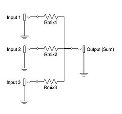
A simple three-channel passive additive mixer. More channels can be added by simply adding more input jacks and mix resistors.
Additive mixers
Mixing console
Additive mixers add two or more signals, giving out a composite signal that contains the frequency components of each of the source signals. The simplest additive mixers are simple resistor networks, and thus purely passive, while more complex matrix mixers employ active components such as buffer amplifiers for impedance matching and better isolation.
Multiplicative mixers
Ideal multiplicative mixers produce an output signal equal to the product of the two input signals. Multiplicative mixers are often used in conjunction with an oscillator in the communications field to modulate signal frequencies. Multiplicative mixers can be coupled with a filter to either up-convert or down-convert an input signal frequency, but they are more commonly used to down-convert to a lower frequency to allow for simpler filter designs, as done in superheterodyne receivers. In many typical circuits, the single output signal actually contains multiple waveforms, namely those at the sum and difference of the two input frequencies and harmonic waveforms. The output signal may be obtained by removing the other signal components with a filter. (see intermediate frequency)
Mathematical treatment
The received signal can be represented as

and that of the local oscillator can be represented as

For simplicity, assume that the output I of the detector is proportional to the square of the amplitude:


![+E_{{\mathrm {sig}}}E_{{\mathrm {LO}}}\left[\cos((\omega _{{\mathrm {sig}}}+\omega _{{\mathrm {LO}}})t+\varphi )+\cos((\omega _{{\mathrm {sig}}}-\omega _{{\mathrm {LO}}})t+\varphi )\right]](https://wikimedia.org/api/rest_v1/media/math/render/svg/d72a321d600a268523eec565645c4375f7a7148c)


The output has high frequency (, and ) and constant components. In heterodyne detection, the high frequency components and usually the constant components are filtered out, leaving the intermediate (beat) frequency at . The amplitude of this last component is proportional to the amplitude of the signal radiation. With appropriate signal analysis the phase of the signal can be recovered as well.


If is equal to then the beat component is a recovered version of the original signal, with the amplitude equal to the product of and ; that is, the received signal is amplified by mixing with the local oscillator. This is the basis for a Direct conversion receiver.


Implementations
Multiplicative mixers have been implemented in a wide variety of ways. The most popular are Gilbert cell mixers, diode mixers, diode ring mixers (ring modulation) and switching mixers. Diode mixers take advantage of the non-linearity of diode devices to produce the desired multiplication in the squared term. It is a very inefficient method as most of the power output is in other unwanted terms which need filtering out. Inexpensive AM radios still use diode mixers.
Electronic mixers are usually made with transistors and/or diodes arranged in a balanced circuit or even a double-balanced circuit. These are readily manufactured by using the technology of either monolithic integrated circuits or hybrid integrated circuits. These are designed for a wide variety of frequency ranges, and they are mass-produced to tight tolerances by the hundreds of thousands, making them relatively cheap components.
These double-balanced mixers are very widely used in microwave communication systems, satellite communication systems, and ultrahigh frequency (UHF) communications transmitters and receivers, and in radar systems transmitters and receivers.
Gilbert cell mixers are just an arrangement of transistors that multiplies the two signals. The switching mixers (below) pass more power and usually insert less distortion.
switching mixers use arrays of field-effect transistors or (in older days) vacuum tubes. These are used as electronic switches, to permit the signal to go one direction, then the other. They are controlled by the signal being mixed. They are especially popular with digitally controlled radios.
What Mixers Are Used with PA Systems?
Mixers are items of equipment that arrange multiple input audio signals in a suitable balance, and they adjust tone quality so that the output audio is easy for the audience to listen to. There are many types and models of mixer.
Types of mixer
Mixers are broadly classified into three types, based on their internal structure.
(1) Analog mixers

Analog mixers adjust the volume and tone of input audio signals. Most of the control knobs and faders are arranged on the top panel, so it is easy to understand the signal flow and what state the audio is in. Operating analog mixers is normally an intuitive process.
(2) Digital mixers

Digital mixers process input audio signals and adjust their volume and tone using digital signal processing technology. Various kinds of tone control that would be impossible using analog equipment can be applied using digital processing. Digital mixers can store the positions of faders and knobs, and recall these positions in an instant. The faders and knobs perform various functions, so the unit itself remains compact, even if the number of channels increases. Generally a digital mixer will require more experience to set up effectively, but will offer far greater functionality than an analog mixer.
(3) Powered mixers

Powered mixers are analog mixers with built-in power amplifiers. For this reason, sound can be played with the mixer directly connected to speakers. In cases where the same equipment is always connected, powered mixers can be used by simply turning the power on, so operation is simplified and convenient.
Reference: All-in-one PA systems

All-in-one PA systems consist of a powered mixer, speakers and speaker cables. They are easy to configure, easy to carry due to their light and compact format, and suited to small events and band lineups.
Input channels
Number of microphone input and line input channels
The number of input channels in a mixer is extremely important, as this indicates the number of microphone and musical instrument signals that can be handled. In addition to the number of input channels in a mixer, it is also important to consider such factors as how many of those input channels are for microphones, whether line input channels are monaural only, and whether inputs will accept stereo signals.
For example, when using a mixer with a band, at least eight channels for input may be required for microphones to pick up the sound of the whole drum kit. In this case, a model that is equipped with enough channels that are compatible with microphones should be chosen.
For example, when using a mixer with a band, at least eight channels for input may be required for microphones to pick up the sound of the whole drum kit. In this case, a model that is equipped with enough channels that are compatible with microphones should be chosen.
A mixer with many stereo channels is useful for connecting multiple devices that output stereo signals, such as synthesizers. Likewise, a mixer that has built-in effectors, such as compressors or reverberation, is recommended for situations where audio such as vocals will be input. Finally, a mixer that is able to connect to a personal computer via USB is recommended for home studio applications.
Differences between microphone input and line input

- Microphone input channel
Audio signals picked up by a microphone are very weak, so they must be amplified by using the head amplifier (GAIN) of the mixer. Connect to the MIC connector.
Note: Phantom power (often labelled as "+48V") is required when using a condenser microphone.
Note: Phantom power (often labelled as "+48V") is required when using a condenser microphone.
- Line input channel
Line level devices such as keyboards and CD players are connected to the LINE connector.
Generally, phone connectors and RCA pin connectors are used in this case.
When both MIC and LINE inputs are available on same channel, use the LINE connector. When the same connector is used for both MIC and LINE, reduce the level by pushing the PAD button so that audio is not distorted (Remember line signals have a higher level than mic signals).
Tips
Sometimes a combination jack is used as both a microphone and a line connector. Activate the PAD when using a line input, to avoid distorting the louder signals.Mixer Functions
This section describes how to adjust the audio of each channel
(1) Equalizers
Mixers are equipped with equalizers that adjust the tone of each channel. Some equalizers have just 2-bands, which can adjust lows and highs. Some are 3-band equalizers, which modify the sound by boosting and cutting lows, mids, and highs. And some 3-band equalizers include a MID-sweep, which can modify the mid frequencies which characterize most musical instruments and voices. The more frequency bands there are, the more detailed the sound production can be.
| Knob | Characteristic | Affected sounds | Boost Effect | Cut Effect |
|---|---|---|---|---|
| HIGH | 10 kHz (+/- 15 dB) | High overtones exceeding the register of the instrument. | Crunchy, metallic echoing increases, and the tone becomes sharp. If boosted too much, will sound noisy. | Tones become smooth. "S" noise canceling is effective. If cut too much, high range transparency will be lost. |
| MID | 3 kHz (+/- 15 dB) | Instrument/vocals high registers | Sound becomes bright and hard. Sound becomes modulated and bright. If boosted too much, sound will become unpleasant. | Audio balance tends toward lows. If cut too much, audio will become dark. |
| 1 kHz (+/- 15 dB) | Instrument/vocals medium registers. | The outline of the audio can be made clear. Audio sounds as if it is projected forward. Emphasizes the attack of toms and bass drums. | Tones become rounded and pleasant. Sounds are more muffled and no longer stand out in the mix. | |
| 500 Hz (+/- 15 dB) | Instrument/vocals medium-low registers. | The sound becomes thicker and more powerful, and tonal balance tends toward lows. If boosted too much, the sound becomes unnatural, as if it were coming out of a telephone. | The sound becomes hard and has a feeling of attack. Tonal balance tends toward highs. If cut too much, the sound becomes thinner. | |
| LOW | 100 Hz (+/- 15 dB) | Instrument low registers. | The sound becomes rounder and deeper, giving it more strength and a sense of scale. If boosted too much, the sound becomes less crisp. | The sound takes on a lighter quality, improving its crispness. Floor noise or howl canceling is effective. |

(2) HPF (High Pass Filter)
The HPF cuts unnecessary low frequencies at the input. Most microphone and mic/line inputs have an HPF function, but some dedicated line inputs may not.
HPFs are often used for hi-hat, snare, and vocals to cut unnecessary low frequencies and therefore create a cleaner sound. They are also used to eliminate unwanted popping noises when picking up voices, such as during speeches.

(3) Pan
This adjusts the output ratio when playing audio from left and right speakers. It is used to widen the sound image, or to position each input relative to their location on the stage. Audio for stereo channels is already set in the stereo image, so a BAL control is used to adjust the balance between the left and right speakers.

(4) Level Faders/knobs
These adjust the volume of each channel, group, stereo output, etc. Fader-type controls allow for quick operation. Though some mixers use knob-type volume controllers.
How to output audio from the mixer?
Mixers can output various separate channels of audio, depending on the needs of the event, such as sending audio meant for the audience to the main speakers and audio meant for the performers to the monitor speakers on stage:
STEREO OUT is normally used to send signals to the audience; AUX SENDs for performers' monitor speakers and external devices; MONITOR OUT is for monitor speakers used when mixing audio in the studio; GROUP OUT for outputting several signals together; REC OUT for connecting with recording devices; and PHONES for connecting headphones.
STEREO OUT is normally used to send signals to the audience; AUX SENDs for performers' monitor speakers and external devices; MONITOR OUT is for monitor speakers used when mixing audio in the studio; GROUP OUT for outputting several signals together; REC OUT for connecting with recording devices; and PHONES for connecting headphones.
(1) AUX bus
The AUX bus is a circuit used to send signals to external devices. It can be used to send signals to performers' monitor speakers separately from the main output, or to send signals to external effects and recording devices. A mixer with many AUX sends should be chosen if there are many people in the band or if separate monitor signals with individual balances need to be sent to the performers.
(2) GROUP bus
The GROUP bus is a circuit for controlling multiple channels at once. For example, if there are eight microphones (for eight channels) placed around a drum set and you want to raise or lower the volume of the entire set, it would be difficult to accurately raise or lower the faders for all eight channels. If these channels are all set to a single group, the volume of the entire drum set can be raised or lowered, while maintaining the same balance, merely by raising or lowering the fader for the group.
(3) STEREO bus
The STEREO bus is a circuit for combining each input coming into the mixer or each GROUP bus signal, adjusting the overall level, and outputting the audio through stereo output connectors.
Sample Function Mixer : Music Electronic
This document is intended for A-100 users who want to learn a little bit about the technical details of the A-100. We will start with some electronic basics and introduce at first the most important electronic parts used in the A-100 circuits. Then we will show how some basic circuits (like attenuators, amplifiers, mixers, inverters and so on) can be realized with these parts. The following paragraph will show some simple modifications of A-100 modules: e.g. changing the sensitivity of CV or audio inputs, increasing or decreasing output levels (e.g. VCAs or mixers with maximum amplification > 1), adding offset feature to mixers, changing between DC and AC coupled inputs/outputs, adding feedback inserts for VC resonance to all filters and many more.
This page starts September 2004. New items will be added little by little. If you have any suggestion for this page please send your ideas to hardware@doepfer.de. We will try to fulfil all wishes, providing they are possible and will not contain confidential information.
Additional information about technical details (e.g. CV/gate control principles, A-100 bus, A-100 power supply) and mechanical details (frontpanel measures, A-100 frame concept) is available in these documents:
The A-100 service manual is available only for A-100 customers (see price list for current price). The words - mainly building, testing and adjustment notes for the manufacturer - are in German but the schematics, silk screen and bill of material are international.
Other pages of interest for DIY:
| |||||||
1. Electronic Parts
(For some parts different signs are shown. Normally the left one is used in USA or Japan, the right one in Germany or Europe) | |||||||
Fixed resistors
A resistor is determinded by these parameters:
In the A-100 normally only resistors with 1/4W (250mW) and 5%, 1% or 0.1% tolerance are used. For the value and tolerance of a resistor normally a color code is used (should we add the color code at this place ?).
| |||||||
  |
Potentiometers
Potentiometers are available as rotary potentiometers or fader types. Normally, a potentiometer has 3 terminals: two end terminals and a slider terminal (upper picture). The slider touches a resistance surface that is located between the end terminals. Sometimes the second end terminal is not shown (lower picture) if only one end terminal is required, e.g. if the part works only as a variable resistor rather than a voltage divider.
A potentiometer is determined by these parameters:
The characteristics - sometimes even called law - is a very important parameter of a potentiometer. This parameter describes the connection between the rotary angle (resp. fader position for fader potentiometers) and the resistance value between terminal 1 and slider terminal. Typical characteristics are linear, logarithmic and inverse logarithmic. Sometimes special characteristics are used (e.g. S-type law) but these are not very common. For audio attenuation normally logarithmic potentiometers are used as the human ear senses the loudness of an audio signal in a logarithmic way too. The same applies to potentiometers that are used to control time parameters (e.g. attack/decay/release time of an envelope generator). For attenuation of control signals normally linear potentiometers are used. For special functions inverse logarithmic potentiometers are used (e.g. resonance/emphasis control in filter circuits).
Another special type is a stereo potentiometer: two potentiometers with one common axis. The values for the two potentiometers vary in the same way. Used e.g. for manually controlled filters or stereo applications. Other special types of potentiometers are not described here (e.g. dual potentiometers with 2 concentric axis, or potentiometers with additional terminals) as they are not used in the A-100.
A very special circuit is a so-called vactrol. This is a combination of a light depending resistor (LDR) and LED both put into a small 100% light-proof case. For details please refer to the vactrol document.
The above pictures shows the type of potentiometers used in the A-100 system. These potentiometers are equipped with a mounting bracket that increases the mechanical stability. For most of the A-100 modules the potentiometers (together with the sockets) are used to mount the pc boards to the front panels.
The A-100 potentiometers are available as spare parts with these values: 10K (A and B), 50K (A, B and C), 500k (B), 1M (A and B) with A = logarithmic (audio type), B = linear and C = inverse logarithmic (ususally for filter resonance controls used). For prices please look at the price list. | ||||||
  |
Trimming potentiometers
The electronic function of a "normal" potentiometer and a trimming potentiometer is the same. The only difference is the mechanical appearance: trimming potentiometers are normally much smaller and have a very short axis that is adjusted with a screw driver. Trimming potentiometers are used to adjust parameters that have to bet set once at the factory and that are normally not controlled by the user (e.g. offset frequency and scale of a VCO, maximum/minimum limitation of values, adjustment of click/pop feedthrough of sound processing devices like VCA, VCF, ring modulator, frequency shifters and so on). Sometimes users replace trimming potentiometers with normal ones to have access to such additional parameters.
Trimming potentiometers are available normally only linear. Apart from that they are defined by the same parameters as normal potentiometers. | ||||||
Capacitors
A capacitor is determinded by these parameters:
In the A-100 all types of capacitors are used. Value, voltage and tolerance are normally written as normal characters on the component (e.g. 4n7 63V). But even color codes and number codes are used (e.g. 103 means 10x1000=10000). Sometimes it is difficult to find the value of a capacitor. E.g. "100" without additional pF/nF could mean 100pF or 100nF. Some experience is required to find out the correct value if the declaration on the component is not readable, or complete. To be certain of a capacitors value, one could use a capacitor measuring instrument such as a multimeter with capacitor measuring option.
So-called electrolytic capacitors are used for values of 1uF and more as the other types of capacitors would be too large. Normally electrolytic capacitors are polarized (i.e. one has to pay attention to positive and negative terminal of the part). If there are "+" or "-" signs in a schematic this means that an electrolytic capacitor is used. The three examples on the left with "+" and "-" signs denote an electrolytic capacitor.
Other types of capacitors (e.g. variable capacitors) are not used in the A-100.
| |||||||
Diodes
Electronic part that works as one-way for electric current. The triangle terminal (left) of the symbol is the positive side (or anode), the single vertical line (right) is the negative terminal (or cathode). Used e.g. for clipping, rectifying or overvoltage protection. Even light emitting versions (LED) available in different colors (red, green, yellow, orange, blue, white). In this case the brightness is approximately proportional to the current.
A very special circuit is a so-called vactrol. This is a combination of a light depending resistor (LDR) and LED both put into a small 100% light-proof case. For details please refer to the vactrol document.
| |||||||
  |
Transistors
Different types of transistors are available, e.g. bipolar npn or pnp, field effect (FET). A transistor can be used with the suitable circuit (i.e. with additional resistors and capacitors) e.g. as amplifier, switch or current source.
| ||||||
 |
Operational Amplifiers
Operational amplifiers are special integrated circuits that make available a standard amplifier with 2 inputs (inverting and non-inverting input) and high amplification (typ. > 1000). Circuits with one, two or more opamps (abbreviation for operational amplifier) are available. The following table shows the pin-out of the most popular types of single, dual and quad opamps.
The power supply pins (marked with the "+" and "-" triangles) of the integrated circuit in question have to be connected to +12V and -12V for A-100 applications. In schematics the power supply pins of opamps are often omitted. The left opamp symbol includes the power supply pins. The right symbol is without the power supply pins.
Unused OpAmps (if e.g. only 3 devices of a quad opamp are used) have to be terminated in this way: non-inverting input has to be connected to GND, inverting input and output have to be connected (directly or even via resistor in the 1k...100k range). | ||||||
Switches
A lot of different switches are available. There exist different distinguishing marks, e.g.:
The pictures show from top to bottom the symbols for a simple on/off switch (SPDT with one ON contact only) , a change-over switch (SPDT with two ON contacts), a rotary switch with 3 positions, a change-over switch with middle position (SPDT with ON-OFF-ON) and a rotary switch witch 5 positions.
| |||||||
 |
Jack sockets
Standard sockets used in the A-100 for all inputs and outputs. Provided that a plug is inserted into the socket the GND and tip terminals of the plug are connected to the corresponding terminals of the socket. The tip is normally the "hot" pin, i.e. the terminal leading the CV resp. audio signal. The sockets are equipped with switching contacts (the arrow in the symbol). Both the GND and tip terminal are switched but only the switching feature of the tip terminal is used in some A-100 modules. Provided that no plug is inserted into the socket the switched tip contact (arrow terminal in the left symbol) is connected to the "normal" tip contact (the terminal represented by the horizontal line in the left symbol). As soon as a plug is inserted this connection is interrupted and the signal at the tip of the plug is connected to the tip terminal of the socket. This feature can be used for default connections (i.e. connection within a module that is established provided that no plug is inserted into the corresponding socket). Example: internal default connections of the A-109 signal processor. This function is often called "normalling" or "normalizing".
The above pictures show the type of jack sockets used in the A-100 system. For most of the A-100 modules the sockets (together with the potentiometers) are used to mount the pc boards to the front panels. The A-100 sockets are available as spare parts. For prices please look at the price list.
| ||||||
Power Supply
For each circuit, a power supply is required. The three symbols to the left side denote +12V, -12V and GND. Some circuits may require no power supply (e.g. multiples or the simple attenuator below) or only a positive supply. All circuits that use operational amplifiers require all three +12V, GND and -12V. Some modules even require +5V (mainly "digital" modules with digital circuits - like microprocessors, memories, or logic circuits - which often require a +5V power supply).
| |||||||


2. Basic circuits
| |
 |
Simple attenuator
This is a simple passive attenuator (i.e. no power supply required). J1 is the input socket, J2 the output socket. A typical value for P2 is 10k...100k. A linear or logarithmic type can be used for P2 (logarithmic especially for audio applications as the loudness characteristics of the human ear is approx. logarithmic).
|
 |
Simple lowpass
This is a simple passive lowpass with 6dB/octave slope. A non-inverting amplifier can be added at the output (and even at the input) to make the circuit independent of input/output impedance (i.e. the "loads" connected to J1 resp. J2). Replacing of R1 by a vactrol leads to simple voltage controlled lowpass filter. Replacing R1 by a potentiometer leads to a simple manually controlled lowpass filter
Frequency of the lowpass: f = 1/(2 * Pi * R1 * C1) with Pi = 3.14
Example: R1 = 47kOhm, C1 = 10nF -> f ~ 340 Hz |
 |
Simple highpass
This is a simple passive highpass with 6dB/octave slope. A non-inverting amplifier can be added at the output (and even at the input) to make the circuit independent of input/output impedance (i.e. the "loads" connected to J1 resp. J2). Replacing of R1 by a vactrol leads to simple voltage controlled highpass filter. Replacing R1 by a potentiometer leads to a simple manually controlled highpass filter
Frequency of the highpass: f = 1/(2 * Pi * R1 * C1) with Pi = 3.14
Example: R1 = 10k, C1 = 2,2n -> f ~ 7.2 kHz |
 |
Non-inverting amplifier
This is a simple non-inverting amplifier: The term "non inverting" means that the polarity of input and output signal are the same. In other words: a positive input signal applied to J1 will cause a positive output signal at J2 and a negative input signal applied to J1 will cause a negative output signal at J2.
The amplification of this circuit is 1 + R1/R2.
Example 1: R1 = 0 Ohm (connection), R2 omitted -> A = 1 Example 2: R1 = 47k, R2 = 47k -> A = 2 Example 3: R1 = 100k, R2 = 10k -> A = 11
If R1 or R2 is replaced by a potentiometer the amplification can be adjusted. If e.g. R1 in the last example is replaced by a 100k potentiometer the amplification is adjustable in the range 1...11. This circuit can be used to built an simple amplifier if the desired audio or CV signal is too small for a certain application.
Attention ! The minimum amplification of this circuit is 1 (no real attenuation possible provided that no external attenuator is used).
|
 |
Inverting amplifier
This is a simple inverting amplifier: The term "inverting" means that the polarity of input and output signal are opposite. In other words: a positive input signal applied to J1 will cause a negative output signal at J2 and a negative input signal applied to J1 will cause a positive output signal at J2.
The amplification of this circuit is - R2/R1 (" - " indicates the opposite polarity of input and output)
Example 1: R1 = R2 = 47k -> A = - 1 Example 2: R1 = 10k, R2 = 100k -> A = - 10 If R2 is replaced by a potentiometer the amplification can be adjusted. If e.g. R2 in the last example is replaced by a 100k potentiometer the amplification is adjustable in the range 0...-10. This circuit can be used to built an simple (inverting !) amplifier if the desired audio or CV signal is too small for a certain application.
The minimum amplification of this circuit is zero (if R2 = 0). To obtain a non-inverted output another inverting amplifier with amplification - 1 has to be used.
The inverting amplifier can be extended by adding more input sockets (J1) and corresponding input resistors (R1). The right terminals of all input resistors are connected to the inverting input (-) of the operational amplifier O1. The relation between the corresponding input resistor R1 and R2 (the same for all inputs) defines the sensitivity of the input in question. If all resistors have the same value (e.g. 100 kOhm) the amplification is "1" for all inputs. Lowering R1 (e.g. 47k or 22k) increases the sensitivity of the input in question. Increasing R2 (e.g. 220k or 1M) increases the amplification resp. sensitivity for all inputs simultaneously.The minus terminal of the operational amplifier is often called "virtual GND" in this circuit as the voltage measured at this point is very close to GND within a few millivolts - independent of the incoming voltages!
The first circuit example (chapter 3: "CV mixer with offset function") shows a typical application of inverting amplifiers with several inputs.
|
 |
Voltage clamping / limiting / clipping
This is a circuit that limits an incoming voltage to the range U1-UD2 ... U2+UD1. The voltage U1 has to be less than U2. UD1 and UD2 are the forward voltages of the diodes D1 and D2. To keep these voltages as small as possible Schottky diodes (e.g. BAT42) ore germanium diodes are recommended because their forward voltages are in the 0.2...0.3V range. R works as a serial protection resistor. A typical value for R is 1k.
A typical application is the limitation of an analog voltage to 0...+5V (e.g. for the inputs of Pocket Electronic or USB64). In this case U1 is connected to GND and U2 to +5V.
Another application is sound distortion by voltage clipping. If U1 and U2 are variable voltages (e.g. outputs of operational amplifiers of one of the circuits in this document) the clipping levels can be voltage controlled too.
|
3. Circuit examples
| |||||
| |||||
| |||||
| |||||
| |||||
| |||||
| |||||


4. Module modifications
| |
| 4.1. General modifications (not for one module only) | |
| 4.1.1. Changing the sensitivity of manual controls, control voltage inputs and audio inputs | |
| The following picture shows the control voltage input circuit for most of the A-100 modules: | |
 |
P1 is the manual control of the corresponding parameter (e.g. tune for a VCO, frequency for a VCF, manual gain for a VCA, manual phase shift for a phaser and so on). P1 generates the voltage U1.
J1 is the (first) input socket for the external control voltage. P2 is the corresponding attenuator. The slider of P2 outputs the voltage U2. Additional CV inputs with our without attenuators may be available (e.g. two or more CV inputs for frequency control for a VCF). The dashed line in the picture is the common point in the circuit where all CV's are added. The output voltage of the circuit (output of O1) is used to control the corresponding parameter (tune, filter frequency, gain ...) of the module in question. The output voltage is defined by:
The relations R3/R1 resp. R3/R2 determine the sensitivity of the corresponding control (P1) resp. input (J1/P2). If for example all resistors are 47k (a common value in the A-100) the sensitivity is 1 for each input. Provided that R3 remains unchanged the resistors R1 and R2 determine the sensitivity of the corresponding control resp. input. Reducing the resistance of R1 resp. R2 increases the sensitivity of the manual control (P1) resp. input (J1/P2). Increasing the resistance of R1 resp. R2 reduces the sensitivity. To modify the sensitivity of a control knob (P1) or CV input (J1/P2) the corresponding resistor R1 resp. R2 simply has to be changed.
Changing the resistance of R3 has the opposite effect and affects the sensivity of both the manual control and CV input. |
| The audio input circuit for most A-100 modules is similar but the manual control P1 is absent (a DC offset would not make sense for an audio input, audio signals are AC signals). Normally only one audio input is available but there are exceptions (e.g. VCA A-130 and A-131, signal processor A-109). To change the sensitivity of an audio input simply the resistor R2 connected to the slider P2 of the audio input has to be replace. A smaller value will increase the sensitivity and consequently lead to clipping/distortion for higher input levels. Especially for the first A-100 VCFs and VCAs (A-120, A-121, A-122 and first versions of A-130, A-131) the audio inputs have been designed to avoid distortion with standard A-100 signals (e.g. VCO). Lowering the input resistors will allow distortion for these moduls too.Even the input resistors of CV or audio mixers (e.g. A-138a/b) can be changed to allow "real" amplification (i.e. > 1). The factory values of the resistors in the mixer modules A-138a/b allow a maximum amplification of about 1 (which is not really amplification). Reducing the input resistors (R2 type) or increasing the feedback resistor (R3 type) will increase the amplification of the circuit. The factory values of the corresponding resistors (R1, R2, R3) for all modules can be found in the A-100 service manual. Normally they are in the 100k range (~ 47k...220k). | |
| 4.1.2. Insert sockets for external resonance control of filters, phasers and similar modules | |
| To enable voltage control of resonance for filters insert sockets in the feedback loop can be used. | |
 |
The left picture shows the resonance control in a filter or phaser circuit. Essentially it is an attenuator that controls the feedback of the circuit. To enable external control of the resonance external access to the feedback loop is recessary.
For resonance control normally C-law potentiometers are used (i.e. inverse logarithmic, e.g. 47kC). |
 |
This is the first solution how to install the insert sockets (pre resonance control). J1 is connected to the slider of the resonance control. Provided that no plug is inserted into J2 the function of the module is unchanged as the switching contact of J2 is active.
As soon as a plug is inserted into J2 the default connection is interrupted and the signal fed to J2 is used as feedback signal. Consequently J1 and J2 can be used to insert e.g. an external VCA to control the resonance. J1 has to be connected to the audio input of the VCA, J2 to the audio output of the VCA. The resonance control can be used to adjust the maximum resonance available with different gain settings of the external VCA. But not only a VCA but any audio processing module can be inserted into the feedback loop (e.g. phaser, spring reverb, waveshaper, limiter, wave multiplier, divider, ring modulator, frequency shifter, or even another filter).
|
 |
This is another solution how to install the insert sockets (post resonance control).
The location of the resonance control at the pc board for all modules in question can be found in the A-100 service manual.
|
| 4.1.3. Changing between AC and DC coupling | ||||
There are two types of coupling between electronic circuits:
Example: minimum frequency = 50Hz, in/output resistance = 10kOhm -> C ~ 2 uF (u = micro = 1/1000000). A usual value would be 2.2uF in this example. AC coupling is normally used for audio signals. For audio signals AC coupling has the advantage that unwanted DC shares in the signal are removed. For some AC processing circuits (e.g. amplifiers, filters) DC voltages are not allowed in the input signal. Therefore very often a capacitor can be found in the input stage of such circuits. DC coupling means that both DC and AC parts of a signal are transmitted. For control voltages (normally) only DC coupling can be used as even fixed voltages (e.g. coming from a manual control) have to be transmitted. In a module patch each A-100 module can be treated as an electronic circuit that is connected to another one. Consequently one has to take into consideration the type of coupling (AC or DC) between modules as the strict differentiation between AC and DC applications os softened for some A-100 modules. E.g. a VCA can be used to process audio signals (i.e. normally AC coupled signals) as well as slowly changing CV voltages (e.g. envelope or modulation amount). Therefore one needs to know if a VCA used is AC or DC coupled. Another example is a divider (e.g. A-115 or A-163) as even these module can be used to process audio or (slow) clock/gate signals. | ||||
 |
Luckily it is not very complicated to switch between AC and DC coupling. All one has to do is to bride (i.e. short circuit) the capacitor in case of an AC coupled in/output. The left picture shows how the switch is connected in parallel to the AC coupling capacitor (the broken line resistor symbol represents the load to GND that is always available in each circuit as reference to GND). If AC coupling is required for a DC coupled in/output simply a capacitor has to be added.
From the schematics it can be seen if an in/output is AC or DC coupled. We will add this information also to the user's manual for modules that may be used for both types of coupling.
For some circuits resp. modules changing from AC to DC coupling is not possible. E.g. the "old" VCAs A-130 and A-131 (those with CEM3381 or CEM3382) are AC coupled as the special CEM circuits cannot be DC coupled because of the internal negative reference voltage. The "new" VCAs A-130 and A-131 (those with CA3080) are DC coupled and can be used to process CV signals too.
A list with the type of coupling for all modules in question will follow soon. For most of the modules the question about the type of coupling does not arise. E.g. all filters are AC coupled and all CV generating and processing modules (e.g. ADSR, LFO, slew limiter, Theremin, Ribbon controller, random voltage) are DC coupled. But for other modules the type of coupling is not obvious (e.g. VCA, divider, waveshaper).
| |||
| 4.1.4. Subsequent bus normalling of modules | ||||
Only the modules A-110 (Standard VCO), A-111 (High end VCO), A-140 (ADSR), A-185 (Bus Access) and A-190 (Midi Interface) have access to the CV and Gate signal of the A-100 bus. A-185 and A-190 are used to "write" the bus, i.e. they output the signals to the bus. A-110, A-111 and A-140 are able to "read" the bus, i.e. they pick up the signals CV (A-110, A-111) resp. Gate (A-140) from the bus. For details please refer to the user manuals of these modules. If other modules should be able to "write" or "read" the bus the module in question has to be modified.Examples:
| ||||
| ||||
| ||||
| 4.1.5. Subsequent socket normalling of modules | ||||
| coming soon ....(how to make use of unused switching contacts of sockets for module pre-patching) | ||||


| 4.2. Specific modifications for certain modulesImportant note: Warranty is void if these modifications are carried out by the customer ! | |
| 4.2.1. A-128 filter bank modification: single outputs | |
| This document shows how to add single outputs to the filter bank A-128 | |
| 4.2.2. A-136 Modification: bypassing the internal pre-amplifier | |
| Module A-136 contains an internal pre-amplifier that is used to amplify the input signal by about 3.5 before it is processed by the A-136. Especially for low level audio signals (e.g. output from a VCF) this is useful. But for all signals with a level beyond ~ 7V this causes clipping before the internal processing takes place. Especially for the processing of LFOs or unfiltered VCOs this may cause a problem. To bypass the internal pre-amplifier resistor R2 has to be removed (e.g. by pinching off). R2 is the resistor in the upper third of the pcb which is very close to the rear edge. When R2 is removed the amplification of the internal pre-amplifier becomes "1" (which means that it does no longer amplify). In addition one has to pay attention that the knob positions may vary a bit from the front panel printing because of mechanical tolerances of the potentiometers and knobs (i.e. "0" is not always exactly the neutral position for "A", "+A" or "-A") | |
| 4.2.4. A-151 Modification: switch for limiting the number of steps (only for old versions of A-151) | |
| A toggle switch 1-0-1 type is required (i.e. with center position). A hole for the additional switch can be drilled e.g. below the socket I/O4. This is how the switch has to be wired:
| |
| 4.2.5. A-148 Modification (old version): T&H instead of S&H | |
| The new version of the Dual S&H module A-148 has a jumper available for each sub-unit that is used to set the operation mode for the corresponding sub-unit to S&H or T&H. The old version of the A-148 was fixed to the S&H mode. To make available T&H for the old version of the A-148 one has to replace the capacitor C1 (10nF) by a resistor (about 1k). C1 is available twice on the pc board: one for the upper and one for the lower unit. It is also possible to add a switch that is used to switch between S&H (capacitor) and T&H (resistor). | |
| 4.2.6. A-152 Modification: S&H instead of T&H | |
| Normally the eight S&H outputs of the module A-152 work not as S&H but as T&H outputs (details can be found in the A-152 user's manual). To obtain S&H function instead of the T&H function the module has to be modified in that way: A connection has to be made between pin 6 of the microcontroller IC1 (on board A, PIC16F676) and pin 2 of IC6 (on board B, DG408). The 10k resistor R32 next to C5 on board B has to be removed. And that's how it works: the enable pin of the multiplexer DG408 is normally connected to +12V ("high") via resistor R32. Pin 6 of the microcontroller (RC4) outputs a short high pulse whenever the address changes. If the enable pin of the multiplexer (DG408) is connected to this pin (instead to +12V via R32) the T&H function changes to a S&H function as the multiplexer is enabled only for a short time at each address change. Even a toggle switch that selects the desired mode can be connected to the pins and the resistor. | |
| 4.2.7. A-155 modifications/undo modifications: gate reset, manual step debouncing | |
| This document shows how to modify or undo the modifications of the sequencer module A-155: A155_Modifications_Undo.pdfThere are two possible modifications: Modification #1 refers to the behaviour of the gate row. Without this modification the gate output remains "high" if the sequence stops at a position with the corresponding gate switch in the on position. If this modification is carried out the gate outputs turns "low" as soon as the sequence stops. It's an AND wiring of the gate outpout with the start/stop state of the A-155. If the A-155 is combined with the A-154 this modification has to be removed ! Modification #2 is a debounding circuit to avoid multiple triggering if the manual step button is used. This modification limits the maximal clock frequency to some hundred Hz (digital low pass). For normal sequencer applications this is no restriction but if the A-155 is used e.g. as a graphic VCO the modification has to be removed. It is not necessary to remove this modification if the A-155 is combined with the A-154. | |
| 4.2.8. A-155 Modification: changing gate row into trigger row #4 | |
| The factory setting of the function of row #4 of the trigger board is Gate. If one prefers another Trigger row the following modification has to be carried out: The connection marked by the arrow in the picture has to be interrupted. Instead of this a connection between pin 5 of IC2 (CD4053) and the close-by pcb track has to be installed (solder jumper).  | |
| 4.2.9. A-155 Modification: adding sockets for address outputs | |
This is the pinout of the internal 10 pin connector that leads from the small control board to the potentiometer and switch boards: Besides the supply terminals (-12V, GND, +12V) these signals are available:
All modifications should be carried out by experts only as the modules contain charge sensitive devices. We have to point out that warranty is lost if such modifications are carried out. | |
| 4.2.10. Modifying the A-124 Wasp Filter for self-oscillation | |
Soldering a 10k resistor in parallel to R13 (27k) leads to self-oscillation of the filter at the max. resonance setting of the resonance control. R13 is located in the gap between IC1 (CD4069) and IC2 (i.e. the upper CA3080, close to C4/100pF). (Thanks to Pierre Serné for the permission to publish this picture) | |
| 4.2.11. Modifying the A-163 voltage controlled frequency divider for DC coupling | |
| Shortening the electrolytic capacitor C7 (2u2) changes the output from AC to DC coupling. C7 is located between the input and the output socket After this modification the A-163 can be used e.g. for frequency dividing of LFO signals too (only suitable for rectangles). Instead of the short circuit even a switch can be used that switches between AC and DC coupling. The only difference between AC and DC coupling is that in the DC coupled mode the output rectangle switches from GND to ~ +5V while in the AC coupled mode the signal is symmetrically around GND (~ -2.5/+2.5V). Usually even the DC coupled mode can be used for audio signals as most of the audio processing modules (e.g. filters) have an AC coupled audio input that removes the positive offset of the A-163 output in DC coupled mode. | |
| 4.2.12. Modifying the A-165 trigger inverter/modifier for S-Trig input | |
| This document shows how to modify the trigger modifier/inverter for S-Trig input: A165_strig_modification.pdf. The modification is very simple. Just one 100k resistor has to be added between the input socket and +12V. | |
| 4.2.13. Shortening the output protection resistor of A-156, A-170 and other modules | |
Most of the A-100 modules are equipped with a 1k protection resistor at the output. This resistor protects the output of the module against shortening to GND or shortening to another output. In sensitive CV applications (typically driving the CV input of one or more VCOs) these protection resistors may cause a small voltage drop that leads to inaccuracy in the 1V/Oct scale. There are two solutions:
| |
| 4.2.14. Removing the springs of the A-174 joystick module | |
| Method #1: Bend very carefully the four metallic tongues of the corresponding potentiometer that hold the end plate of the potentiometer in question. E.g. a small screw driver could be used. Pay attention not to break off the tongues. Then the end plate and the spring can be removed. Re-install the end plate by bending back the four tongues. This can be done for both or only one of the two potentiometers of the joystick.Method #2:Another possibilitly is to compress the two ends of the spring and cut with a suitable small cutting pliers without dismantling the potentiometer. In this case the remnant of the spring remains in the potentiometer.Pay attention that warranty is lost if the joystick is modified ! | |
| 4.2.15. Meaning of the pin headers of the A-174-2 wheel module | |
 The jumpers JP4 and JP6 are used to install a small voltage plateau around 0V. The plateau appears if the corresponding jumper is removed (normally used for the spring loaded wheel only to obtain 0V output in the neutral position). The jumpers JP4 and JP6 are used to install a small voltage plateau around 0V. The plateau appears if the corresponding jumper is removed (normally used for the spring loaded wheel only to obtain 0V output in the neutral position).The jumpers JP3 and JP7 are used to select the output voltage range (i.e. symmetrical or positive voltage only). Pay attention that this corresponds to the mechanical adjustment of the wheels ! This means one has to re-adjust the wheels also if the jumper settings of JP3 or JP7 are changed. That's a bit tricky and only recommended for experienced users. Otherwise the voltage range of the outputs will be not correct (e.g. not starting with 0V or a large "dead range" for the wheel without spring, or not 0V in the center position of the spring loaded wheel). Pay attention that a re-adjustment of the wheels liable to pay costs if the wheel adjustment has been changed by the customer ! | |
| 4.2.16. Changing the BBD circuit in the A-188-1 BBD module / Adjustment of the A-188-1 BBD module | |
| The following document describes the A-188-1 adjustment procedure: A1881_adjustment.pdf | |
| to be continued | |
5. Simple DIY modules / frames
| |
| 5.1. Attenuator | |
|
This is the simple attenuator circuit mentioned in chapter 2. The two sockets J1 and J2, and the potentiometer P2 can be mounted on a blind panel with 8 HP (4 HP will be a little to small for the potentiometer). To take advantage of the whole 8 HP panel a second attenuator or a small multiple (i.e. some connected sockets) can be mounted on the same panel. A value of 50k is recommended for P2 (linear for CV applications, log for audio applications).
|
| 5.2. Bypass / Bypass with attenuator | |
  |
The left circuit is a simple bypass that can be used to decide if an audio processing module (e.g. a filter or a phaser) is active or not. J1 and J2 form a miniature multiple. J1 is connected to the audio source (e.g. a VCO output or a mixer output), J2 to the audio input of the audio processing module (e.g. filter). J3 is connected to the audio output of the processing module. The position of the switch determines if the audio processing module is active (lower position of the switch) or not (upper position of the switch). The four sockets and the switch can be mounted on a blind panel with 4 HP.
In the right circuit the bypass is expanded by two attenuators (P1, P2) that can be used to compensate possible audio level differences, i.e. no or little audio level changes appear when the switch is operated. One of the attenuators may be omitted if not both levels have to be adjusted. The four sockets, the two potentiometers and the switch can be mounted on a blind panel with 8 HP. 50k log is recommended for P1 and P2.
|
5.3. Self-construction of A-100 frames
| |
 |
The left picture shows the construction of the standard 6 HU A-100 frame (A-100G6). The construction is described in detail in this document:
The standard 6 HU frame is made of the following components:
A detailed description of the A-100 frame construction is available as pdf document A100G6_e.pdf
The most expensive parts of the frame are the side plates, mounting flanges and top/bottom covers. If you do not care much for a 19" compatible housing a low cost version of an A-100 frame can be built according to the following instructions.
Pay attention that this is suitable for qualified personnel only who are able to ensure the electrical safety of the final construction. On no account beginners or laymans are allowed to assemble frames. Dangerous mains voltage 115V / 230V. Danger to life !
|
 |
From the parts list above only the front rails version 1 with "lip" and threaded inserts (1) and the accessory screws are required (the screws that are used to mount the rails to the side plates in the standard version of the frame). Around these 4 rails a suitable case has to be constructed as outlined in the left picture. The rails and accessories are available from the German company ProMA (www.proma-technologie.de) but there are many other companies on the market too. Even rails longer than the 19" standard can be used to obtain bigger non-19" frames (from ProMA e.g. rails with 1m length are available).
At the rear of the case the A-100 power supply (A-100NT12 or A-100PSU2, with mains inlet, power switch and fuse holder) and the bus boards have to be mounted with distance sleeves or spacers.
The wiring of the power supply and the bus boards is described in this document:
As these works affects parts, pc boards and cables that conduct mains voltage (230/115V) carrying out of these works is allowed only for experts or authorized personnel who are familiar with all valid safety rules. Laymen are not allowed to carry out these works ! Danger to Life.
|
6. Miscellaneous
| |
| 6.1. A-100 Power Supply | |
The A-100 requires a bipolar/symmetrical power supply with -12V, GND and +12V. A high quality linear power supply is recommended. Switching power supplies are not recommended. We tried several switching power supplies for A-100. The main advantages of switching power supplies would be the wide range AC input (typ. 90-240V AC, i.e. no supply modification if you move e.g. from USA to Europe and vice versa), low price and small shape/weight. As some customers suggested switching supplies we ordered three types of switching supplies with different power (Meanwell, Sun Power, Condor/SL) and installed them into standard 6U/84HP cases and a 12U/168HP monster case. For all tested supplies the results are very poor. The main problem is the unsufficient load regulation that may lead to VCO tuning problems. We found up to 200 mV (=0.2 V) voltage change of the +/-12V supplies while the load changes. Such load changes are caused e.g. by different LED illuminations (normally a module will consume more current if a LEDs is bright compared to the dark state) or other effects (e.g. frequency changes of VCO/VCF). If the linear A-100PSU2 was used the +/-12V changed only by about 5mV under the same conditions. Consequently switching power supplies can be recommended only for "non-critical" DIY applications (e.g. if only CV sources/modifiers and audio modifiers are installed). For frames that include one or more VCOs we recommend the A-100PSU2 or another linear supply with good load regulation (10 mV or better).
| |
Selecting the Right Mixer
At the most basic level, an audio mixer does exactly what its name implies: mix audio signals. If you have more than one sound source (say, five microphones, an electric guitar, a bass, and a keyboard), you need a mixer to combine these audio signals so that you can control the relative balance between them before sending the summed signal to a loudspeaker system, recording device, etc. Because every signal comes into and out of the mixer, investing in a quality product is crucial and will save a lot of operational headaches.
Here are a few things to consider:
- Channel count. Also known as “frame size,” a mixer’s channel count determines how many sources can be connected to its channel inputs simultaneously. For example, a 24-channel mixer will allow you to connect at least 24 audio sources, although there may be additional specialized inputs, such as Tape and Talkback inputs. Some smaller-format consoles provide stereo channels in addition to mono channels. Stereo channels are counted as two inputs, even if they share a single channel. This is important to keep in mind as you make your selection.
- Connection types. In addition to knowing how many sources you’ll connect to your mixer, it’s important to know the types of sources. If you plan to mostly connect microphones, make sure to select a mixer with enough microphone preamps. If you will connect line-level sources, make sure your mixer has at least a few line inputs to reduce the need for direct boxes.
- Aux buses. Most mixers can send at least one monitor mix to the stage. This is typically done with auxiliary buses—“aux buses” for short. Each channel is equipped with a level control for each aux send. You build your monitor mix by setting the individual aux-send levels for any channels you want to be heard in that mix. The aux bus output can then be connected to a stage monitor or in-ear system. If you use aux buses exclusively for monitors, the number of aux buses you have determines the number of discrete monitor mixes you can create. Keep in mind that aux buses are usually mono, so a stereo monitor mix for in-ear systems will require two aux buses. Calculate your needs accordingly.
- Analog or digital. In general, there are two flavors of mixer: analog and digital. An analog mixer relies on electrical circuits and filters, whereas a digital mixer converts the analog signal into digital audio data that is sent to an onboard processor. After processing, the signal is converted back to the analog domain, where it can be sent out to speakers, personal monitoring systems, and so on. While both mixer types will provide basic level and pan control, each has advantages and disadvantages. In general, an analog mixer will be more affordable and simpler to use; digital mixers tend to be more complex but offer more functionality. We’ll discuss this in more detail later.
- Onboard signal processing. Most mixers will have some onboard signal processing on each channel, on each bus, or both. The more signal processing available on your mixer, the less money you will have to spend on outboard gear. In general, digital mixers provide considerably more signal processing than analog mixers, commonly including at least some dynamics processing and EQ. It’s also convenient to have reverb and delay effects built in. Make sure that onboard effects have their own dedicated aux bus, though; otherwise, you may have to sacrifice a monitor mix to add reverb or other effects to vocals and instruments.
- Recording options. Many modern mixers provide some level of integrated recording. This can range from a simple two-track recording of the Main mix to complete multitrack recording, either to an onboard recorder or to a computer or both. When evaluating computer recording options, look for the bus type (USB, AVB, FireWire, etc.), included software, and recording bit depth and sample rate. Most modern mixers with recording features offer 24-bit recording at 44.1 kHz or higher.
Analog Mixer Basics
At their core, most analog mixers share many of the same features and functions. The biggest advantage of analog mixers is that they’re generally less complicated and less expensive than digital mixers of the same frame size. The disadvantage is that analog mixers usually have fewer onboard features than digital mixers, and their sound quality depends entirely on the quality of the analog circuitry.
Some analog mixers, like PreSonus® StudioLive® AR-series analog mixers, use great-sounding analog circuitry, provide EQ on every channel, offer at least a few monitor mixes, and include at least a basic onboard effects processor for reverb and delay effects. StudioLive AR-series mixers also feature PreSonus’ unique, flexible Super Channel, which allows you to connect four stereo line level devices, including wireless stereo Bluetooth™ input.
Many modern analog mixers also offer digital recording features. The most common implementation is a simple onboard 2x2 USB interface that allows you to record the main mix. Less common is the ability to record each channel individually. StudioLive AR-series mixers take this further, offering professional 24-bit, 96 kHz multitrack recording (every input channel, plus the main mix) over USB, as well as a separate onboard stereo SD recorder that enables you to quickly record the main mix or play hours of stereo recordings.
Digital Mixer Basics
Digital mixers include the basic functions provided by their analog cousins and add many tools that save you money by eliminating the need for expensive outboard equalizers, compressors, noise gates, multi-effects processors, and the like. While you don’t need these processors just to mix audio, they are essential for producing better-sounding, more polished mixes. All these tools are done courtesy of an onboard digital signal processor (DSP). This processor is responsible for routing, level control, and so on. Full-featured digital mixers provide plenty of graphic and parametric EQ, dynamics processing, and more.
Traditionally, the complexity of digital mixers made them more difficult to learn but PreSonus StudioLive digital mixers changed that, providing a wealth of onboard signal processing without forcing you to dive into multiple layers and menus. The StudioLive’s surface-driven workflow has made them one of the most popular mixers in the world. Because the parametric EQ, compression, noise gate, and limiter are available on every input and output, you save the cost of outboard gear and mountains of cables, as well as the hassle of connecting it all.
Digital mixers also provide tools to address the problem of managing complex mixes. Population groups reduce the channels you’re viewing at one time. DCAs (Digitally Controlled Amplifiers) control the overall level of a group of channels.
 StudioLive Series III consoles, StudioLive Series III rack-mount mixers, and StudioLive RML rack-mount mixers combine the best aspects of these solutions with Filter DCAs. A Filter DCA can contain any combination of available input channels and effects returns, and you can create as many Filter DCA groups as you need. StudioLive Series III and RML mixers allow you to include the same channel in multiple Filter DCAs so you can manage mixes in multiple ways. Each group is given a master level control so you can control the overall level of the group while maintaining each channel’s relative balance in the mix. In this way, for example, you can create a single fader to control every drum in a monitor mix and maintain the relative level of the drum mix that you created. You can even create a custom User fader bank that includes individual channels and Filter DCA group masters to simplify mixing even further. This is especially useful if a member of your band also doubles as your front-of-house engineer.
Both analog and digital mixers have long been available as traditional consoles and in rack-mount format. Rack-mount analog mixers and older digital rack mixers are usually controlled with knobs and perhaps small faders. But today’s digital rack mixers are more often controlled with a laptop, a tablet, a smartphone, or a networked hardware controller.
Let’s take a closer look at these two approaches:
Digital Console Mixers
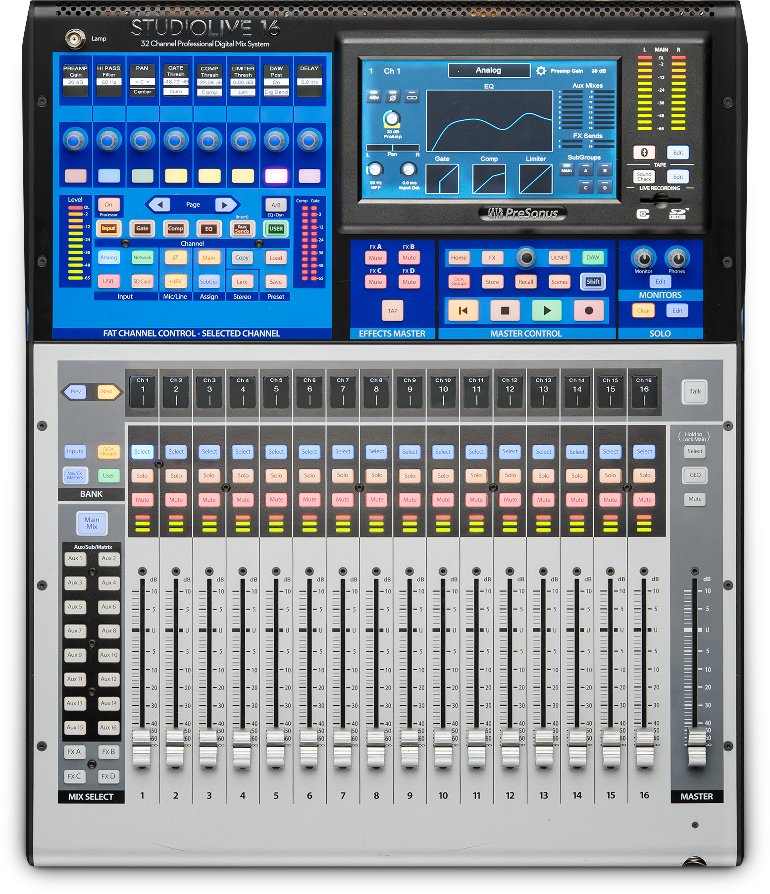 Digital console mixers, such as the StudioLive Series III mixers, typically look like their analog cousins, in that the analog front end and mixing controls are housed in the same chassis. Many modern consoles allow some level of modular capability, allowing you to network stage boxes and other mixers so that your inputs and outputs can be closer to the sources and destinations.
The benefit of a networked system is that you save quite a bit of money, time, and frustration with long cable runs and traditional stage boxes, using a single CAT5 or CAT6 cable to carry literally dozens of audio streams back and forth. Another advantage is flexibility, as the channels on your mixer can be sourced locally or from the network. This allows you customize and reorient your system as your needs change.
Digital Rack Mixers
As their name indicates, many newer digital rack mixers, including the StudioLive RML series and StudioLive Series III rack mixers, are designed to sit in an equipment rack onstage with the musicians. This makes connections more convenient and reduces the need for long cable runs that can introduce noise into your system. This also saves cost on expensive snakes and stage boxes.
Digital rack mixers typically have few, if any, onboard controls. This type of mixer relies on two methods of control: mobile devices and hardware controllers.
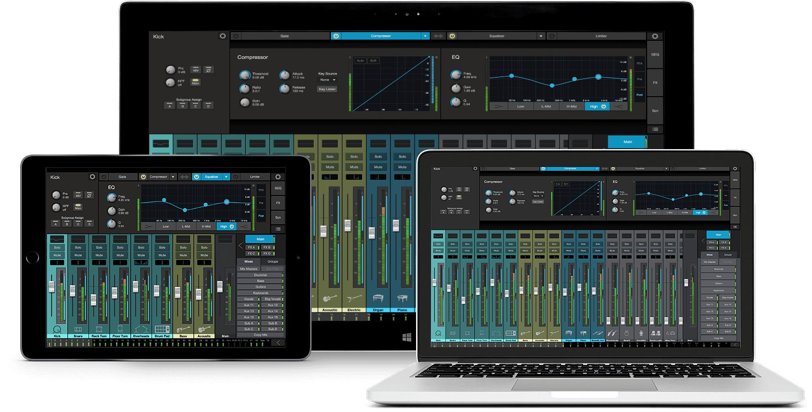 Control applications, such as PreSonus UC Surface for Apple iPad®, Android™ tablet, Mac®, and Windows® provide wireless access to all mixing functions. These control apps are very flexible and highly mobile, enabling you to mix anywhere within wireless range of your mixer. However, for people who are accustomed to a traditional mixer, this may be disorienting at first.
For those who want to control their digital rack mixer using hardware, without running a long copper snake from the stage to front-of-house, hardware controllers like the StudioLive CS18AI provide the best of both worlds. The StudioLive CS18AI connects to its digital rack mixers with a relatively inexpensive, lightweight Ethernet cable, enabling very long cable runs with no signal degradation.
Connection Types
Once you’ve selected the type of mixer, the next consideration is the type of connections you’ll need. In general, most mixers feature the following types of connections:
- XLR microphone inputs. For the most part, XLR input connectors are used for microphone preamps and inputs. Usually, they can accept both dynamic and condenser microphones. It should be noted that condenser microphones require phantom power, so if you plan to use them, make sure your mixer has that feature. Some XLR inputs on certain mixers are switchable between mic and line level signals. If this is the case, you will not need a direct box to connect a line-level source.
- ¼” TRS Line Inputs. TRS, or Tip-Ring-Sleeve, line inputs are balanced connections used for line-level devices like synthesizers and outboard processors.
- Aux Inputs. Most mixers provide the ability to connect additional sources to your mixer. These inputs typically are not equipped with processing and are intended for use with consumer electronics, like DVD players. Examples of unbalanced connections are RCA and 1/8-inch TRS connections.
Bus Types
Auxiliary Buses
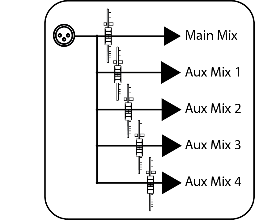 As its name implies, an aux mix allows you to create an alternate, or “auxiliary,” mix that can be routed to an output separate from the Mains. Aux buses have many applications, the two most common of which are creating monitor mixes and inserting external effects processors into the mix. When you turn up the aux send level on a channel, its signal is sent to the corresponding aux output at the level you choose. In this way, the same channel can be used to create several alternate mixes to the main mix.
Most mixers have some ability to send at least one monitor mix to the stage. This is typically done with auxiliary buses (aux buses for short). Let’s say a mixer has one aux bus. On a mixer like this, each channel would have an aux send level control. This control adjusts the volume of each channel in the aux bus mix. You build your monitor mix by setting the individual aux-send levels for any channels you want in that mix. The aux mix output can then be connected to a stage monitor or an in-ear or headphone distribution system. In this way, your musicians can listen to a monitor mix that can be controlled separately from the main mix going out to the house.
If you’re thinking an aux send sounds a lot like a channel fader, you’re way ahead of the game. Just as each channel fader allows you to create a mix for the main output, each aux send allows you to create a mix for the corresponding aux bus output. (Aux sends can also be used for other things like routing controlled amounts of signals to outboard effects.)
If you’re using aux buses exclusively for monitors, the number of aux buses determines the number of discrete monitor mixes you can create. Most lower-cost mixers have one or two. Two aux buses provide two separate mixes, six aux buses provide six separate mixes, and so on. Note that aux buses and their sends are typically mono, so a performer who needs a stereo monitor mix (such as a keyboardist using stereo in-ear monitors) will need two aux buses: one for the left side of the mix, one for right. Keep this in mind when determining how many aux buses you need.
Creating custom monitor mixes is critical. If musicians can’t hear themselves or their bandmates, their performance will suffer. A monitor mix can be mono or stereo. Most often, an individual live monitor mix is mono and is sent to a floor-wedge or sidefill monitor (the obvious exception being in-ear monitor systems). A studio monitor mix is usually stereo because it is sent to a headphone amplifier that requires both a left- and a right-channel input. In both cases, the function of the aux bus is the same.
Another use for an aux mix is to send selected channels to an external effects processor. The processed signal is then patched back to the mixer, usually using an aux input. There are at least two main advantages to creating an effects mix instead of inserting an effect on a channel. First, several channels can be sent to a single processor. In addition to greatly simplifying the number of parameters you must control, this can help to create a cohesive sound for your mix. Second, you can vary the level sent from each channel to the processor, rather than patching the output directly into the effect. This allows you to add a lot or a little of an effect to any given channel.
Subgroups
A subgroup allows you to combine multiple channels into a single bus so that the overall level for the entire group is controlled by a single fader and can be processed as a mix, in addition to the processing available for each channel. Subgroups can also be soloed and muted. You will find many uses for subgroups that will make mixing more convenient and will provide better control of your mix.
Grouping individual instruments that create a section in your mix has obvious advantages: The entire group can be muted or soloed, brought up or down in a mix, and faded in or out for a more polished intro or outro. Because subgroups can also be processed, some common groups are drums, backing vocals, horn sections, and string sections.
Another use for a subgroup is to route specific channels to a subwoofer or a front fill, using the same mix as the main front-of-house system. This is especially useful for subwoofers because you can route only the sources that can be reproduced by the subwoofer, allowing you to run your system more efficiently.
Matrix Mixes
On the simplest level, a matrix mix is a mix of mixes. A matrix mix allows you to combine any bus on your mixer, along with input channels. Matrix mixes can be a Swiss Army knife for solving some of the most problematic audio routing issues.
Common uses for matrix mixes are:
- Feeding the house mix to multiple locations (e.g., the lobby, a webcast feed)
- Creating a front fill mix
In some venues, the house PA doesn’t cover the front rows effectively. This can be especially problematic when the band onstage is using in-ear monitors instead of floor wedges. Without floor wedges, the people seated in the first few rows may actually be “behind” the PA because they will hear more stage volume from the instruments on stage than from the front-of-house system. This problem can be solved by placing a few low-profile fill speakers on the front edge of the stage to cover the first few rows of the audience and using a matrix mix to blend the main left/right mix at a low level with source signals that may be difficult to hear, like the vocal and direct bass channels. StudioLive Series III mixers make this easy by allowing you to mix inputs and outputs for each matrix mix.
Solo Bus
When mixing live, or when recording multiple musicians at once, it is often necessary to quickly listen to just one instrument or group. The solo bus can be used with the monitor bus (if available) to provide the front-of-house engineer with a way to isolate channels in a dedicated mix, without affecting what the audience and musicians hear.
In general, there are three different types of solo options: AFL, PFL, and SIP.
- AFL (After-Fader Listen). AFL sends the channel or subgroup signal to the solo bus post-fader so that you can control the level of the soloed signal with the fader.
- PFL (Pre-Fader Listen). PFL sends the channel or subgroup signal to the solo bus before it reaches the fader so the fader does not affect the soloed signal.
- SIP (Solo In Place). This is also known as “destructive solo.” When channels are soloed in this mode, every channel that isn’t soloed will be muted, and only the soloed channels will be sent to their assigned outputs. While useful for dialing in dynamics during soundcheck, this mode is dangerous during a live show.
Remote Mixing from Anywhere
Although the mixer is the core of a good PA system, it is often tucked out of the way because of space constraints, to hide the cables and the mixer’s flashing lights and to keep the mixer safe from curious or inebriated audience members. The problem is, hiding the mixer usually means locating the sound person away from the “sweet spot.” (The “sweet spot” is the middle position between the two sides of a sound system, where sound reproduction is the most accurate, making it easier to dial in a great mix.)
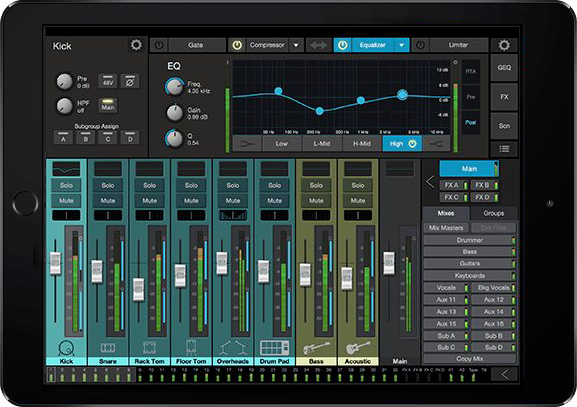 When the mix position is not centered within the optimal listening area, you’ll get a lot of exercise running to the ideal listening position, listening for problems, running back to the mixer to correct the problems you heard, and then running back to the sweet spot to verify the problems were corrected. The traditional alternative is to send an assistant out to listen in those locations and report back. Obviously, neither is a desirable way to mix.
Most modern digital mixers solve this by allowing you to remotely control the mixer from a tablet, smartphone, or laptop. This allows the mixer to be placed pretty much anywhere in the venue. This can also be useful when a member of the band also has to act as the audio engineer because they can mix from the stage.
Applications like PreSonus UC Surface allow you to wirelessly control both the front-of-house and monitor mixes, input and output processing, routing, and more from anywhere in the venue. Whether an audio engineer or crew member wants to walk around the venue and onstage to check the mixes, or the bass player is dialing in the front-of-house mix, they can do so with complete wireless control of the mixer.
Remote Monitor Mixing
Large venues and major touring acts generally employ a separate monitor mixer near the stage, in addition to the main mixer at front-of-house. The front-of-house engineer handles the main mix, while the monitor engineer focuses on the needs of the band. This is a luxury that most bands and smaller venues can’t afford. Digital mixers like the StudioLive Series III and StudioLive RML series solve this with an application that runs on a mobile device connected wirelessly to the mixer. The app gives each musician onstage control over their own monitor mix.
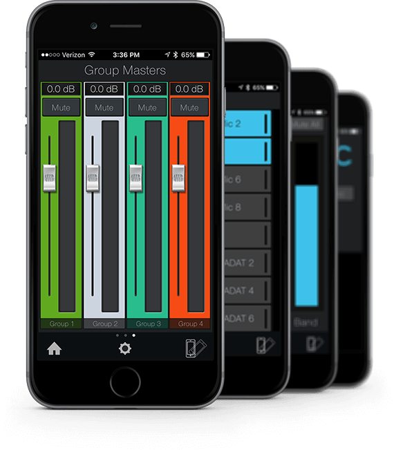 For example, PreSonus QMix®-UC gives up to 16 musicians control over the relative mix levels of their own monitor mixes and makes creating these mixes easy with the Wheel of Me view. This lets you select multiple "Me" channels and turn them all up in your monitor at the same time, while controlling the relative balance between “Me” and the rest of the band.
More advanced users can have complete control of the aux-mix send level and panning (for linked auxes) for each channel from the Aux view. These users can also create four custom groups. This allows them to divide complicated mixes into something more manageable by providing a master fader for a group of channels, while still maintaining the relative balance between them. This is especially useful for drums.
Recording in the Studio and Live
The professional solution for recording to a computer is an audio interface, such as the PreSonus Studio 192 series and Quantum series. An audio interface converts analog signals to digital and vice versa, routing digital audio to and from a computer, most often via USB or Thunderbolt. If you’re recording live in front of an audience, you already have all your instruments and microphones connected to a mixer, so the problem becomes figuring out how to get the signals into your audio interface at the same time. This isn’t impossible, but it involves advanced setup, cabling, and more than a little audio know-how.
Many modern mixers, including all PreSonus mixers, remove this hurdle by building in a professional audio interface that allows you to simply connect the mixer to your computer and hit record in your favorite DAW application – no analog cabling involved.
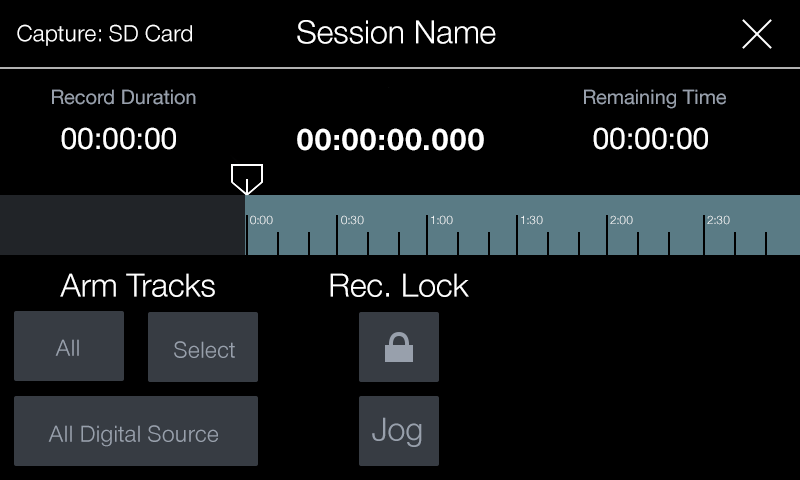 PreSonus mixers make this even easier by including both Capture™ and Studio One® for free. Using Capture is especially easy because the software knows which StudioLive mixer you’ve connected to your computer and automatically creates a track for every input channel and a stereo track for recording your main mix. Capture makes recording even easier with its unique Record Now feature. This button creates a new session, arms all tracks for recording, and starts recording instantly with one mouse click.
StudioLive Series III console mixers take this one step further by providing an onboard 34x34 SD recorder with Capture built in, allowing you to create multitrack recordings without a computer. These consoles can simultaneously record to a computer over USB or AVB. StudioLive AR-series and StudioLive Series III rack mixers provide an onboard stereo SD recorder that lets you capture the main mix.
Whether recording live or in the studio, the next step is to mix in a controlled environment. This allows you to add processing, remove microphone handling noise, and level out fluctuating signals. To do this, you’ll need a digital audio workstation (DAW) application. To this end, PreSonus StudioLive mixers include Studio One, a powerful, yet easy-to-use, professional recording and mixing application for Mac and Windows. Of course, StudioLive mixers are compatible with other DAWs that support Core Audio (Mac®) or ASIO (Windows®) but Studio One offers many advantages, including tight integration with StudioLive mixers.
If you have a StudioLive mixer, you can start by simply recording the stereo mix in real time directly to the stereo track in Capture or to the SD recorder. But you don’t have to choose between recording a stereo mix and recording individual tracks.
Recording stereo mixes has disadvantages, especially if you’re simply recording the main mix that is also feeding your house speakers. Let’s say the guitar amp is loud enough in the house that it doesn’t need to be reinforced through the main sound system. If the guitar is not in the front-of-house mix, a recording of that mix won’t include guitar except to the extent the guitar bleeds in through the microphones. Vocals are typically very loud in the house mix so they can be clearly heard; if you record the house mix, your recording probably will be too vocal-heavy. Multitrack recordings are a better solution because they avoid these issues and offer flexible mixing and editing capabilities.
Once you’ve mixed your song, you can upload it directly to SoundCloud from Studio One and push it out to your fans immediately.
Get a Good Soundcheck, Even if the Drummer’s Stuck in Traffic
Another great way to use your recordings is to soundcheck before the whole band arrives. This is where virtual soundcheck can save time and frustration. As its name implies, virtual soundcheck allows you to check the band’s sound without the band. Many modern digital mixers provide some way to do this—some more complex than others—but very few have a true virtual soundcheck that is completely integrated into the mixer. StudioLive mixers provide this amazing experience through Capture’s unique Virtual Soundcheck mode.
 Once Capture is launched, just click the Virtual Soundcheck button and pick one of the recorded live performances you have stored on the computer. This will load the recorded audio onto the tracks in Capture, complete with track names, and engage all digital returns on the StudioLive mixer. You can now play back audio through the system and dial in the mix before the band arrives. StudioLive Series III mixers take virtual soundcheck to the next level by allowing you to use a recording on an SD card, enabling soundcheck without a computer.
Virtual soundcheck also comes in handy when musicians are running late, enabling you to dial in a great mix while you’re waiting. When everyone has arrived, simply click the Virtual Soundcheck button again to remove the audio from the Capture session, disengage all the digital returns on the mixer, and arm every track in Capture for recording so you can record the rehearsal or service. Track names in Capture are broadcast throughout the StudioLive network, so when virtual soundcheck is done, the channels on your StudioLive mixer, UC Surface, and QMix-UC are labeled and ready to go.
Using Background Tracks
Large touring acts use background tracks to sound arena-sized and to replicate the sound of their albums. If your mixer provides digital returns from your computer, as with StudioLive mixers, this is easy even for the smallest bands. The first step is to record backing tracks in advance. For playback, press the appropriate Digital Return buttons on the StudioLive to route the tracks back through channels on the mixer. These tracks can be as simple as a full stereo mix or as advanced as individual tracks that members of the band have previously recorded to embellish a performance. The keyboardist, for example, might prerecord some orchestral tracks and play the main piano part live.
In some situations, you’ll want one or more members (usually at least the drummer) playing to a click track. A click track is basically just a metronome that makes it easy to sync the live performance with the prerecorded tracks. Since you don’t want the audience to hear the click, mute the corresponding mixer channel in the main mix and just send the click to the aux sends for the appropriate performers’ monitors.
Doing More with Multitrack Recordings
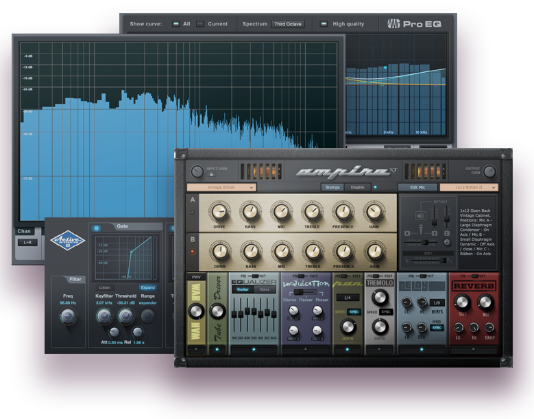 Multitrack recordings can be a great way to attract new fans, but as with performances, you want to put your best foot forward. While the stereo mix you record in real time and upload to a service like SoundCloud can be a great way to get quick social media promotion, it’s probably not the best quality you can achieve. This is where the integration between Capture, StudioLive, and Studio One comes in.
As mentioned earlier, you can simply launch Studio One and open your Capture Session. Unlike most DAWs, bringing in additional tracks or loading plug-ins is as easy as drag-and-drop from Studio One’s browser. (A plug-in is software that provides processing such as reverb, delay, compression, and EQ within a host recording application.) From within Studio One, you have access to a complete suite of signal-processing plug-ins and everything else you need to create a polished, professional quality mix of your performance. You also can use compatible third-party plug-ins.
Plug-ins can be used for processing during the gig, as well as in the studio .
Pulse-width modulation (PWM) or duty-cycle variation methods are commonly used in speed control of DC motors. The duty cycle is defined as the percentage of digital ‘high’ to digital ‘low’ plus digital ‘high’ pulse-width during a PWM period. Fig. 1 shows the 5V pulses with 0% through 50% duty cycle.
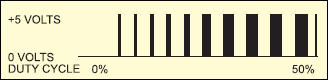
The average DC voltage value for 0% duty cycle is zero; with 25% duty cycle the average value is 1.25V (25% of 5V). With 50% duty cycle the average value is 2.5V, and if the duty cycle is 75%, the average voltage is 3.75V and so on. The maximum duty cycle can be 100%, which is equivalent to a DC waveform. Thus by varying the pulse-width, we can vary the average voltage across a DC motor and hence its speed.
Circuit Diagram
The circuit of a simple speed controller for a mini DC motor, such as that used in tape recorders and toys, is shown in Fig. 2.
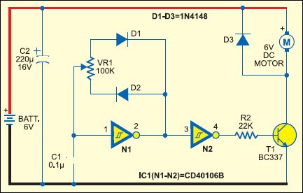
Circuit Operation
Here N1 inverting Schmitt trigger is configured as an astable multivibrator with constant period but variable duty cycle. Although the total in-circuit resistance of VR1 during a complete cycle is 100 kilo-ohms, the part used during positive and negative periods of each cycle can be varied by changing the position of its wiper contact to obtain variable pulse-width. Schmitt gate N2 simply acts as a buffer/driver to drive transistor T1 during positive incursions at its base. Thus the average amplitude of DC drive pulses or the speed of motor M is proportional to the setting of the wiper position of VR1 potmeter. Capacitor C2 serves as a storage capacitor to provide stable voltage to the circuit.
Advertisement
Thus, by varying VR1 the duty cycle can be changed from 0% to 100% and the speed of the motor from ‘stopped’ condition to ‘full speed’ in an even and continuous way. The diodes effectively provide different timing resistor values during charging and discharging of timing capacitor C1.
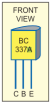
The pulse or rest period is approximately given by the following equation:Pulse or Rest period ≈ 0.4 x C1 (Farad) x VR1 (ohm) seconds. Here, use the in-circuit value of VR1 during pulse or rest period as applicable.
The frequency will remain constant and is given by the equation:
Frequency ≈ 2.466/(VR1.C1) ≈ 250 Hz (for VR1=100 kilo-ohms and C1=0.1 µF)
The recommended value of in-circuit resistance should be greater than 50 kilo-ohms but less than 2 mega-ohms, while the capacitor value should be greater than 100 pF but less than 1 µF.
XO___XO Xi D W Wireless and Test & Measurement
Test & Measurement matrix switches to tier one wireless testing laboratories around the world. These RF matrix switching systems allow for wireless test lab automation providing repeatable, recordable and remotely controlled testing. Our global customer base includes network service providers, network equipment, chipset, and device and UE manufacturers. This automation is critical for the complex, ever changing wireless environment referred to as 4G, 5G WiFi, LTE, LTE-U, IoT, commonly referenced with regard to convergence and the networked society. The company also provides lab management software that allows for scheduling multiple remote users, bringing cost and resource efficiency to a critical part of the product development and verification process and improving ROI. Quintech lab automation products and software, accompanied with millisecond switching speeds, enable the emulation of free space in a controlled environment. 
Test & Measurement matrix switches to tier one wireless testing laboratories around the world. These RF matrix switching systems allow for wireless test lab automation providing repeatable, recordable and remotely controlled testing. Our global customer base includes network service providers, network equipment, chipset, and device and UE manufacturers. This automation is critical for the complex, ever changing wireless environment referred to as 4G, 5G WiFi, LTE, LTE-U, IoT, commonly referenced with regard to convergence and the networked society. The company also provides lab management software that allows for scheduling multiple remote users, bringing cost and resource efficiency to a critical part of the product development and verification process and improving ROI. Quintech lab automation products and software, accompanied with millisecond switching speeds, enable the emulation of free space in a controlled environment.


Heterogeneous Network Test Equipment :
Test equipment for the ever more complex HetNet infrastructure including beam forming antennas, self-optimized networks (SON) and distributed antenna system (DAS) for rapidly evolving wireless platform .
MIMO Test Lab Automation :
The architecture of the Matrix Switch enables emulation of free space in a controlled environment by allowing controlled summing of signals from any combination of the inputs.
Wireless Mesh Network Test Bed:
Wireless Mesh Network Test Bed: Multi-hop wireless mesh networks can be a very cost effective network for supporting large distributed communications with applications ranging from mobile wireless broadband to Military usage. Testing mobility of mesh networks involves physically moving devices around inside the shield room of the lab or using simulation techniques with questionable accuracy. Accurate test environments require a combination of the two. This is accomplished by putting wireless nodes into RF shielded enclosures. Antennas are removed and replaced with cables that connect wireless devices to the Quintech mesh network test solution which includes any-to-any connections with on/off switching and attenuators to simulate distance. Using this solution, devices can be interconnected with attenuation creating diverse network topologies with complete reproducibility. The switches can be remotely reconfigured in milliseconds, changing connections and attenuations. Such a test bed can used for testing LTE Direct devices, WiFi mesh routers, Machine-to-Machine (M2M) mesh, small cells mesh backhaul and SON interference control, ad-hoc and sensor networks. Quintech’s wireless mesh network test bed is a scalable, controllable and cost-effective solution for these technologiesThermal Expansion of Electronic Components
 Electronic components are used in the automotive, communication, aerospace and other industries. Miniaturization, higher package density and accelerated development processes have a great impact on the reliability of electronic components.
Rapid changes of ambient temperature or internal production of heat may occur during operation. This may create high thermal stresses due to the mismatch of the thermal expansion coefficients of the different materials in electronic components.
The electronic components used in cars are exposed to high stress due to vibrations and extreme temperature changes. If a car is started the temperature of the electronic cards might pass a value of minus 0°C to a value beyond 140°C in a few minutes. Today, a big amount of the car recalls by the manufacturers are due to electronic malfunctions.
The thermal expansion is very important for the durability of electronic components. Joining of different materials exposed to variations of temperature generates the strain mismatch which can be locally strong. These strains might cause cracks which initiate malfunctions.
Strain mismatch occurs by the following process:
- During the production process (soldering conditions, heat production during curing, …)
- During the operation due to local production of heat (Resistant loses microprocessors, diode laser, …)
- Changes of ambient temperature
On the other side simulations (FEM, …) are used in the electronic industry, but the material parameters (coefficient of thermal expansion, young’s modulus, …) have to been known. A validation of results is necessary. In some cases simulations are not possible, than the measurement precise deformation is necessary.
The 3D-ESPI Sensor Q300 is a very powerful tool to investigate the thermal expansion of electronic components. Due to the full field measuring technique combined with a high resolution the determination of critical areas and hot spots in electronic components is very easy.
The 3D-ESPI Sensor Q300 is a very powerful tool to investigate the thermal expansion of electronic components. Due to the full field measuring technique combined with a high resolution the determination of critical areas and hot spots in electronic components is very easy.
Deformation of yaw sensor due to power consumption
The optical sensor head of the Q-300 is placed above the yaw sensor and the PLC44 housing is connected to the power supply. Applying a voltage of 5 V the surface deformation has been monitored during heating up. The power consumption was 1,35 mW.


Measurement setup
In the pictures below, the resulting displacement fields are shown. The maximum displacement in the in-plane direction is the range of ±0,6 µm and in the range of ±0,3 µm for the out-of plane displacement. The displacement field in z-direction shows the place of the sensor (light blue) an the ASIC itself (red).

Thermal expansion of an electronic board
 Here the set-up for the test of a electronic board is shown. No components are mounted on the board but some internal layers are inserted in order to reduce the thermal expansion locally. The board is heated from the backside by thermal radiation and has been heated from room temperature up to 60° C.
The graphics show the displacement fields in the two in-plane directions and the related strain fields. In the strain field εyy the effect of reducing the thermal expansion is clearly seen.

Thermal Expansion of Ball Grid Arrays
Electronic components are used in the automotive, communication, aerospace and other industries. Miniaturization, higher package density and accelerated development processes have a great impact on the reliability of electronic components. Rapid changes of ambient temperature or internal production of heat may occur during operation. This may create high thermal stresses due to the mismatch of the thermal expansion coefficients of the different materials in electronic components. For example the thermal expansion coefficients for typical materials, used in a BGA assembly are shown in the table below:| Gold: | a = 14,2 *10-6/K |
| 95 Sn-5Ag: | a = 23,2 *10-6/K |
| Silicon: | a = 2,6 *10-6/K |
| FR4: | a = 13,0 *10-6/K |
| Dexter Hysol FP4401: | a = 22,0 *10-6/K |
| Ablebond 965-1L: | a = 50,0 *10-6/K |
The variation of the thermal expansion coefficient can be up to a factor of 25. The 3D-ESPI Sensor Q300 is a very powerful tool to investigate the thermal expansion of BGAs components. Due to the full field measuring technique combined with a high resolution the determination of critical areas and hot spots in electronic components is very easy.
Measurement of Ball Grid Arrays (BGA)

Measurement setup

The different components of a BGA assembly
The upper picture shows the measurement set-up. The scheme of the principle of the assembly of a BGA is shown in the second picture. The component is placed in the heating chamber.
Measurement of BGA with and without defect
The thermal expansions of two BGA’s (one without and one with defect) are measured from room temperate up to 140 °C.
The result of the thermal loading at three different temperatures is shown in below. The in-plane displacement fields are quite similar. The bending in z-direction of the sample B shows a different behaviour than the good sample. At approximately 120 °C the middle of the BGA bends in the opposite direction.
The result of the thermal loading at three different temperatures is shown in below. The in-plane displacement fields are quite similar. The bending in z-direction of the sample B shows a different behaviour than the good sample. At approximately 120 °C the middle of the BGA bends in the opposite direction.
| Displacement x-direction | Displacement y-direction | Bending | |
| T = 142°C |  |  |  |
| Thermal expansion of BGA without defect at T=142°C | |||
| T = 142°C |  |  |  |
| Thermal expansion of BGA without defect at T=142°C | |||
Measurement of the fiber reinforced substrate FR4
The measurements are performed with the same setup and the same thermal loading as the measurements of the BGA’s above. Figure d) shows the FR4 sample as seen be the sensor. The results for the in-plane and out-of-plane displacement as well the spatial distribution of CTE’s are shown in the same figure. The upper fiber layer is seen in fig. c) and fig. f).
![Electronic Components: displacement field x-direction [µm]](https://www.dantecdynamics.com/images/content/applications/electronic-components/displacement_x.jpg) | ![Electronic Components: displacement field y-direction [µm]](https://www.dantecdynamics.com/images/content/applications/electronic-components/displacement_y.jpg) | ![Electronic Components: displacement field z-direction [µm]](https://www.dantecdynamics.com/images/content/applications/electronic-components/displacement_z.jpg) |
| a) displacement field x-direction [µm] | b) displacement field y-direction [µm] | c) displacement field z-direction [µm] |
 | ![Electronic Components: CTE for x-direction [10-6 1/K]](https://www.dantecdynamics.com/images/content/applications/electronic-components/CTE_x.jpg) | ![Electronic Components: CTE for y-direction [10-6 1/K]](https://www.dantecdynamics.com/images/content/applications/electronic-components/CTE_y.jpg) |
| d) sample | e) CTE for x-direction [10-6 1/K] | f) CTE for y-direction [10-6 1/K] |
Here you see the difference of the CTE in due to the fiber orientation.

 |  |  |
| a) x-displacement | b) y-displacement | c) z-displacement |
In-plane and out-of-plane displacement fields of a BGA assembly after thermal loading
| ||
Non Destructive Control of Flip Chip Packages
 Flip chip is an interconnection technology where a face-down (or "flipped") electronic components is both mechanically and electrically connected to its substrate in a one step process by means of bumps or solder joints.
This technology offers major improvements over the standard wire bonding technique, especially in terms of number of Inputs/Outputs (I/O), components density and electrical performances at high frequency. Hence flip chip packaging is getting more and more popular in microelectronics industry.
For flip chip, the continuous trend for higher number of I/O and finer pitch translates into higher number of smaller bumps. This makes reliability of flip chip assemblies more and more difficult to achieve both during their manufacturing process and at the component lifetime scale. And with reliability comes another issue: inspection of interconnections as bumps are hidden below the die, preventing visual inspection as for wire bonding. As a consequence, identification of defaults and failure modes in flip chip assemblies required Non Destructive Control (NDC) techniques able to detect very small features such as cracks in a bump, delamination at the bump/chip or bump/substrate interface.
Several NDC techniques such as X-Ray microscopy, Infrared Thermography or Scanning Acoustic Microscopy have been used to this purpose and can offer significant results for inspection of Ball Grid Array (BGA) or flip chip assemblies with rather large bumps (i.e. >100 µm). However, these methods reach their resolution limits for inspection of packages with bumps as small as a few tens of microns. To overcome this limitation, NDC techniques based on optical interferometry with submicron resolution have recently been proposed such as Moiré, laser ultrasound coupled to interferometry or Electronic Speckle Pattern Interferometry described hereafter.
Flip Chip at Alcatel Space
Flip chip assemblies manufactured at Alcatel Space are dedicated to RF applications. Hence, parts to be connected are mainly GaAs Monolithic Microwave Integrated Circuits (MMIC) and ceramic substrates both with gold pads. For that reason, the technology chosen to make flip chip assemblies is thermocompression with gold stud bumps.
Gold stud bumps are made on the substrate thanks to a modified "ball bonding" process. Depending on RF applications, bumps can be stacked in order to obtain double or even triple bumps.


Simple and triple stacked stub bumps
MMICs are then connected to the substrate by thermocompression with a flip chip bonder providing the temperature and pressure required to make the assembly. This technique offers the advantage to allow the use of MMIC off the shelves without any extra process at the wafer level and is also compatible with many ceramic substrates (AlN, Alumina..).
These flip chip assemblies based on stud bumps and developed for RF purposes exhibit several specificities compared to the ones based on solder balls arrays and commonly encountered in digital electronics. First, gold stud bumps are very small: their diameter is limited to 50 µm whereas their height is in the 20 to 80 µm range depending on the number of stacked bumps. Then the number of bumps per chip is very limited: 10 to 20 bumps are often enough to connect all the RF access and DC pads. And finally, bumps are mainly located at the die periphery.
Non destructive control of Flip Chip assemblies
In space industry, quality standards require a systematic visual inspection of connections in hybrids packages. If control does not rise any problem for wire bonding, it becomes a critical issue for flip chip assemblies where bumps performing both electrical and mechanical connections are hidden by the die itself. Then, visual inspection has to be replaced by other Non Destructive Control techniques. The challenge for flip chip packages manufactured at Alcatel Space deals with the very small size of stud bumps to be inspected.
Several techniques were evaluated at Alcatel Space to perform NDC on our flip chip assemblies but the most standard ones were shown to reach their resolution limits. Images obtained by Infrared Thermography for example are affected by all the metal layers deposited at the die surface.
In particular, bumps pads prevent to have a clear picture of bumps themselves. Scanning Acoustic Microscopy was also tested but without success as a trade off has to be made between resolution and penetration depth of the ultrasound into the package. And finally recent X-Ray microscopy set up have allowed the detection of small bumps below the die but without the resolution to identify any defect at the bump level. Moreover, in our particular case with stud bumps located at the die periphery, resolution from these last two methods suffers from edge effects.


3D-Electronic Speckles Pattern Interferometry (3D-ESPI) is an original alternative NDC technique for microsystems inspection. This full field measurement method enables three dimensional deformation analysis of any component without contact and with a sub-micron resolution.
In practice, to measure displacements of the device under test in both the two in plane directions and the out of plane one, four illumination directions are used in the real 3-D ESPI set-up. To prevent any vibration artefact during acquisition, the whole set-up is also mounted on an air cushion table.
Applied to Flip Chip packages inspection, 3D-ESPI measurements are expected to detect different deformations behaviour between assemblies with and without defaults such as missing bumps, open connections or cracks etc.
3D-ESPI measurements on Flip Chip Assemblies
 Flip chip samples were manufactured with 4x5.5mm², 100 µm thin, GaAs MMICs connected to AlN substrates. Chips used in this experiment are test devices with daisy chains to allow electrical control of every connection. Hence assemblies exhibit a large number (up to 130) of double stud bumps located both in the middle of the chip and at its periphery.
Two groups of samples were prepared. The first one is composed of assemblies with all their 130 bumps. The second group consists of flip chip assemblies with defects. In order to evaluate the 3D-ESPI system sensitivity in the first phase of this work, "large" defaults were intentionally introduced and half of the bumps were removed. Then all the remaining bumps were located at the die periphery. In both cases, resistance measurements were performed on daisy chains and indicated that all the contacts were electrically correct both after the flip chip bonding process and after ESPI measurements.
3D-ESPI measurements were performed between room temperature and 125 C. Images of the speckle pattern were recorded every 5 C and deformations of the flip chip packages in the three directions were deduced.


 Out of plane displacement (or z-deformation) experienced by a chip with all its bumps: 0.5 micron z-deformation is observed at the center of the die.
As resistance measurements performed on daisy chains have indicated that all the contacts were electrically correct on this die before and after ESPI measurements, the observed strain can be attributed only to the small coefficient of thermal expansion (CTE) mismatch between the GaAs die (CTE ~ 6 ppm/ C) and the AlN substrate (CTE ~ 4 ppm/ C).
After half of the bumps were removed, the z-deformation at the centre of the die is higher than 3 microns!
 The large difference between these two measurements is summarised on the left with the illustration of the out of plane displacement of both packages along their diagonal. This result clearly indicates that the 3D-ESPI techniques could detect defaults such as missing bumps in flip chip assemblies.
Conclusion
Non destructive control of flip chip assemblies with very small (~ 50 microns) stud bumps was successfully performed by 3D-Electronic Speckles Pattern Interferometry measurements. This method allows measurements of in plane and out of plane displacement of component submitted to thermal loading, and differences in behaviour of good die and dies with defaults such as missing were shown to be detectable.
3D-ESPI System Q-300 TCT

Q-300 ESPI head mounted to a bracket
Thermal Expansion Measurement
- Characterization of electronic components and determination of CTE
The 3D electronic speckle interferometry is a very powerful tool to investigate the thermal expansion of MEMS and electronic components.
Due to the full field measuring technique, combined with a high resolution the determination of critical areas and hot spots in electronic components is very easy.
The 3D-ESPI System Q-300 TCT is designed for complete three dimensional and highly sensitive thermal expansion measurement and strain analysis of materials and components.
- Full field, 3-dimensional measurement without contact and marking
- Delivers CTE and thermal strain
- Measurement of electronic components and materials
Non-contact, full-field and 3D-Analysis on nearly any Material
 Flipchip Assembly (1cm x 1cm) |  BGA with detected de-bonding |
 |  |
| Thermal expansion of o Flipchip with perfect bonding (left) and defect bonding (right) | |
Q-300 TCT has successfully been used in development and testing of complex (anisotropic) materials, components and structures in electronic applications. It is ideal for the experimental verification of analytical and numerical calculations.
The 3D information enables fast determination of the thermal expansion coefficient of materials as well of the thermal stress of components such as printed circuits, BGA, Flip Chip’s, etc.
The measurement is performed non-contact, on the whole measuring area and on nearly any material. The field of view can be adjusted down to square millimetres.
The Q-300 TCT system is fully equipped with a heating device, control electronic and a 3D-ESPI sensor on an adjustable support.
Due to the optional use of a contour module the Q-300 TCT could not only be applied to flat surfaces, but also to curved surfaces.
The sensor is driven by a robust electronic control system with the complete software package ISTRA.
The temperature is acquired at each measuring step. It offers automatic or manual measurement, and quantitative data analysis of 3D displacement and thermal strain fields.
Sub-micrometer accuracy is achieved depending on the geometrical set-up. Maximum measuring accuracy is guaranteed by taking into account the varying sensitivity with different object coordinates. Therefore, the complete geometry matrix is recalculated automatically by ISTRA for Windows® for every object point.
| Technical Data: | Q-300 TCT |
|---|---|
| Measuring Sensitivity: | 0.01 - 0.1 µm adjustable |
| Measuring Range: | Adjustable to any measurement range by variation of measurement steps (10 - 100 µm per step depending on measuring direction) |
| Measuring area: | 40 x 50 mm² down to 0.7 x 1 mm² |
| Operation modes: | automatic, manual, 1D-, 2D-, 3D-operation |
| Data interface | TIFF, ASCII |
| Data acquisition speed: | 3.5 seconds for 3D analysis |
| Data analysis: | automatic serial analysis or manual at any measurement step |
| Dimensions of sensor head: | 80 x 130 x 120 mm³ |
| Dimension of heating device: | 200 x 200 x 70 mm³ |
| Laser (built-in): | Laserdiode, 70 mW, 785nm |
| Processor: | Portable PC with integrated electronics, heating control with timer |
| Operating system: | Windows 2000, XP |
| Heating Specification: | Max. temperature: 300 °C. Heating rate: 30 °C per minute. Heating power: 200 W |
| Mode of operation | Manual or ramp heating. Manual or automatic (timer controlled) measurement |
Options:
- Contour measurement for thermal strain analysis on curved structures
- Different lenses for variable field of views
- Optical table
3D-ESPI System Q-300 TCT
Q-300 ESPI head mounted to a bracket
Thermal Expansion Measurement
- Characterization of electronic components and determination of CTE
The 3D electronic speckle interferometry is a very powerful tool to investigate the thermal expansion of MEMS and electronic components.
Due to the full field measuring technique, combined with a high resolution the determination of critical areas and hot spots in electronic components is very easy.
The 3D-ESPI System Q-300 TCT is designed for complete three dimensional and highly sensitive thermal expansion measurement and strain analysis of materials and components.
- Full field, 3-dimensional measurement without contact and marking
- Delivers CTE and thermal strain
- Measurement of electronic components and materials
Non-contact, full-field and 3D-Analysis on nearly any Material
Flipchip Assembly (1cm x 1cm) | BGA with detected de-bonding |
| |
| Thermal expansion of o Flipchip with perfect bonding (left) and defect bonding (right) | |
Q-300 TCT has successfully been used in development and testing of complex (anisotropic) materials, components and structures in electronic applications. It is ideal for the experimental verification of analytical and numerical calculations.
The 3D information enables fast determination of the thermal expansion coefficient of materials as well of the thermal stress of components such as printed circuits, BGA, Flip Chip’s, etc.
The measurement is performed non-contact, on the whole measuring area and on nearly any material. The field of view can be adjusted down to square millimetres.
The Q-300 TCT system is fully equipped with a heating device, control electronic and a 3D-ESPI sensor on an adjustable support.
Due to the optional use of a contour module the Q-300 TCT could not only be applied to flat surfaces, but also to curved surfaces.
The sensor is driven by a robust electronic control system with the complete software package ISTRA.
The temperature is acquired at each measuring step. It offers automatic or manual measurement, and quantitative data analysis of 3D displacement and thermal strain fields.
Sub-micrometer accuracy is achieved depending on the geometrical set-up. Maximum measuring accuracy is guaranteed by taking into account the varying sensitivity with different object coordinates. Therefore, the complete geometry matrix is recalculated automatically by ISTRA for Windows® for every object point.
| Technical Data: | Q-300 TCT |
|---|---|
| Measuring Sensitivity: | 0.01 - 0.1 µm adjustable |
| Measuring Range: | Adjustable to any measurement range by variation of measurement steps (10 - 100 µm per step depending on measuring direction) |
| Measuring area: | 40 x 50 mm² down to 0.7 x 1 mm² |
| Operation modes: | automatic, manual, 1D-, 2D-, 3D-operation |
| Data interface | TIFF, ASCII |
| Data acquisition speed: | 3.5 seconds for 3D analysis |
| Data analysis: | automatic serial analysis or manual at any measurement step |
| Dimensions of sensor head: | 80 x 130 x 120 mm³ |
| Dimension of heating device: | 200 x 200 x 70 mm³ |
| Laser (built-in): | Laserdiode, 70 mW, 785nm |
| Processor: | Portable PC with integrated electronics, heating control with timer |
| Operating system: | Windows 2000, XP |
| Heating Specification: | Max. temperature: 300 °C. Heating rate: 30 °C per minute. Heating power: 200 W |
| Mode of operation | Manual or ramp heating. Manual or automatic (timer controlled) measurement |
Options:
- Contour measurement for thermal strain analysis on curved structures
- Different lenses for variable field of views
- Optical table
Thermal Comfort
 ComfortSense – A tool for indoor climate studies
 ComfortSense can be used for many applications including:
++++++++++++++++++++++++++++++++++++++++++++++++++++++++++++++++++++++++
e- Control System on WET ON/OFF Automatic ( Work--> Energy --> Time ON/OFF Automatic )
++++++++++++++++++++++++++++++++++++++++++++++++++++++++++++++++++++++++
Tidak ada komentar:
Posting Komentar